1
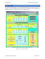
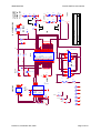
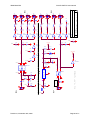
IRAM Plateau de Bure Observatory
POLAR SWITCH
User manual
Philippe CHAVATTE, IRAM - Backend
Revision A, November 18th, 2009
IRAM Back-End
POLAR SWITCH user manual
Table of contents
1.
LIST OF ILLUSTRATIONS....................................................................................................... 2
2.
TABLES ........................................................................................................................................ 2
3.
INTRODUCTION ........................................................................................................................ 3
4.
GENERAL SPECIFICATIONS.................................................................................................. 3
4.1
4.2
4.3
4.4
5.
BACKGROUND ....................................................................................................................... 3
POWER ................................................................................................................................... 4
OPERATING TEMPERATURE RANGE ................................................................................... 4
PRINTED CIRCUIT BOARDS DETAILS .................................................................................... 5
DEVICE CONNECTIONS .......................................................................................................... 6
5.1
5.2
5.3
5.4
5.5
6.
MECHANICAL DETAILS ........................................................................................................ 6
CONNECTORS ........................................................................................................................ 6
INDICATORS .......................................................................................................................... 6
C1 CONNECTOR PIN-OUT...................................................................................................... 7
INTERNAL CONNECTOR PIN-OUT (DIGITAL-SIDE)............................................................... 7
INSTRUMENT INTERFACES .................................................................................................. 8
6.1
6.2
6.3
6.4
6.5
7.
CAN BUS I/O SIGNALS ......................................................................................................... 8
1PPS SYNC INTERFACE.......................................................................................................... 8
RESET BUTTON...................................................................................................................... 8
RS232 SERIAL PORT ............................................................................................................ 8
5MHZ REFERENCE CLOCK ................................................................................................... 8
LOCAL INTERFACES ............................................................................................................... 8
7.1
7.2
8.
ONE WIRE INTERFACE ......................................................................................................... 8
ANALOG VOLTAGES MONITORING ..................................................................................... 8
IMPLEMENTATION DETAILS................................................................................................ 9
8.1
MICRO CONTROLLER UNIT (MCU) .................................................................................... 9
8.1.1
8.1.2
8.1.3
8.1.4
8.1.5
8.1.6
8.1.7
8.2
9.
C164 Micro-Controller Unit (MCU).................................................................. 9
CAN Controller .................................................................................................. 9
Analog to Digital Converter............................................................................... 9
Digital I/O ........................................................................................................ 10
Asynchronous Serial Controller ....................................................................... 10
Synchronous Serial Controller ......................................................................... 10
One Wire controller.......................................................................................... 10
VOLTAGE REGULATORS ..................................................................................................... 10
BUILT-IN FIRMWARE ............................................................................................................ 10
9.1
9.2
10.
BOOTSTRAP LOADER .......................................................................................................... 10
POWER UP OR RESET SEQUENCE ....................................................................................... 10
DEVICE-SPECIFIC SOFTWARE / CAN FUNCTIONS INTERFACE .............................. 11
10.1
10.2
10.3
10.4
OPERATING PROGRAM ....................................................................................................... 11
CAN OVERVIEW ................................................................................................................. 11
SUMMARY OF THE CAN MONITOR POINTS ...................................................................... 11
SUMMARY OF THE CAN CONTROL POINTS ...................................................................... 11
Revision A, November 18th, 2009
Page 1 of 2
IRAM Back-End
10.5
POLAR SWITCH user manual
CAN PAYLOAD CONTENTS ................................................................................................. 12
10.5.1
a)
b)
c)
d)
e)
f)
g)
10.5.2
a)
b)
c)
Monitor points in detail .................................................................................... 12
MODULE_ID....................................................................................................... 12
SERIAL_&_TEMP .............................................................................................. 12
PSU_VOLTAGE1................................................................................................ 12
PSU_VOLTAGE2................................................................................................ 13
MODULE_STATUS............................................................................................ 13
ELAPSED_TIME................................................................................................. 13
LAST_HV_POLAR ............................................................................................. 14
Control points in detail..................................................................................... 14
HV_POLAR ......................................................................................................... 14
INIT...................................................................................................................... 14
CPU_RESET........................................................................................................ 14
11.
TEST SOFTWARE .................................................................................................................... 15
12.
ABBREVIATIONS AND ACRONYMS................................................................................... 16
13.
REFERENCES ........................................................................................................................... 17
14.
POLAR SWITCH DRAWING LIST........................................................................................ 18
1. List of illustrations
Figures:
FIGURE 1: BLOCK DIAGRAM .................................................................................................................................... 4
FIGURE 2: DIGITAL PCB & COMPONENTS LAYOUT (REAL SIZE) .............................................................................. 5
FIGURE 3: MODULE FRONT VIEW ............................................................................................................................. 6
FIGURE 5: THE DB9 MALE CONNECTOR IS SHOWN VIEW FROM THE PIN SIDE ........................................................... 7
FIGURE 6: POLAR SWITCH TEST PANEL ............................................................................................................. 15
2. Tables
TABLE 1: C1, CAN & CONTROL CONNECTOR PIN OUTS .......................................................................................... 7
TABLE 2: J3, RS232 CONNECTOR PIN OUTS ............................................................................................................. 7
TABLE 3: ADC CHANNELS ASSIGNMENT ................................................................................................................. 9
TABLE 4: SUMMARY OF MONITOR POINTS ............................................................................................................ 11
TABLE 5: SUMMARY OF CONTROL POINTS ............................................................................................................ 11
Revision A, November 18th, 2009
Page 2 of 3
IRAM Back-End
POLAR SWITCH user manual
3. Introduction
The aim of the POLAR SWITCH1 module is to select, for each antenna, what horizontal or
vertical polarisation data is to be sent to the correlators. The module can process 12 antenna
and is fully compatible with NOEMA12.
The digital board receives commands through the CAN3 bus, a micro-controller (MCU12)
translates them and drives the switches through two connectors. The switching is
synchronised by the 1pps12 pulse issued from the observatory master clock.
Last switching position, power supply voltages, temperature and IDentification information
can be monitored with few CAN12 commands.
4. General Specifications
4.1
Background
The digital board carries the 1pps12 receiver and 4 drivers, the 5MHz clock receiver
and 4 drivers, connectors and voltage regulators on the motherboard, and a C1646
micro-controller (MCU) located on a daughter board.
The interface between the CAN bus and the switches is a commercial daughter board
with a C164 micro-controller (MCU). It is a derivative of the famous Infineon C1678
family. It receives commands through the CAN bus, computes data and translates
them in switching commands. Interruption routines process CAN receive and the
timing management. Switching update is synchronised by the 1pps12 timing signal.
The MCU can be reset by a local pushbutton located on the mother printed circuit
board.
On the front panel are located the CAN connectors, indicators and switch connectors.
On the rear panel are located the 230VAC connector and main switch, the 5MHz and
the 1pps connectors used to feed WIDEX.
Revision A, November 18th, 2009
Page 3 of 4
IRAM Back-End
POLAR SWITCH user manual
Polar switch
A1 - A6
CAN
RS232
MCU
1 sec
MCU
A7 – A12
1pps
1pps
Clock
Drivers
5MHz
5MHz
Figure 1: Block diagram
4.2
Power
The module requires a +6.5VDC/1.3A unregulated power supply, supplied through J4
connector on the module digital-side.
Total power requirement:
+6.0V to 7.5V / 1.3A
Note: The 2A fuse is located inside the module.
4.3
Operating Temperature Range
All components currently used have standard temperature range specifications of
0 – 70°C.
Revision A, November 18th, 2009
Page 4 of 5
IRAM Back-End
4.4
POLAR SWITCH user manual
Printed circuit boards details
The digital board is a two-layer surface-mount printed circuit board and measures
205mm x 242mm.
Figure 2: Digital PCB & components layout (real size)
Revision A, November 18th, 2009
Page 5 of 6
IRAM Back-End
POLAR SWITCH user manual
5. Device connections
5.1
Mechanical Details
The module is a metal box that measures 250mm x 260mm. Its height is 120mm.
IRAM
POLAR SWITCH MANAGER
Reset
A7 A8 A9 A10 A11 A12
Can
Can
C1
C2
+5
VC
+3 AN
.3
V
+5 DC
VD
-5 C
VD
C
1p
ps
Full NOEMA
A1 A2 A3 A4 A5 A6
Figure 3: Module front view
5.2
Connectors
The module has several connectors located on the top of the module. Connectors are
classified by function as it follows:
- C1 & C2: SubDB9 Connection to CAN bus
- C3: TTL outputs to HV switch Antenna 1-6
- C4: TTL outputs to HV switch Antenna 7-12
- C5: 230VAC/50Hz input (CEE22)
- C6: 1pps input (BNC)
- C7, C8, C9, C10: 1pps output (SMB)
- C11: 5MHz reference input (SMA)
- C12, C13, C14, C15: 5MHz reference output (SMA)
- J3: HE10 Connection to terminal RS232 (Access from inside only, on digital-side)
5.3
Indicators
The module has tree external indicators located on the top of the module. Indicators
are classified by function as it follows:
- L1: 1pps green indicator (flashes when a 1pps signal is received)
- L2: Module powered (flashes when a CAN frame is received or transmitted)
- L2: +5V power supply for the external switches
- L4: -5V power supply for the external switches
Revision A, November 18th, 2009
Page 6 of 7
IRAM Back-End
5.4
POLAR SWITCH user manual
C1 connector pin-out
- C1 & C2: SUBD9 connection to CAN bus
Figure 4: The DB9 male connector is shown view from the pin side
Pin
1
2
3
4
5
6
7
8
9
5.5
Signal
I/O
Function
CAN_SHLD
CAN Shield (Non standard!)
CAN_L
I/O
CAN_L Bus Line (dominant low)
CAN_GND
CAN Ground, connected to board ground
N/C
Not connected
POWER 24V
Power distribution +24V (Non standard!)
CAN_GND
CAN Ground, connected to board ground
CAN_H
I/O
CAN_L Bus Line (dominant high)
N/C
Not connected
POWER 0V
Power distribution return (Non standard!)
Table 1: C1, CAN & Control connector pin outs
Internal connector pin-out (digital-side)
- J3: HE10 connection to terminal RS232 (Access from inside only)
Pin
1
2
3
4
5
6
7
8
9
10
Signal
Dir
Function
N/C
Not Connected
N/C
Not Connected
SERIAL_TxD
O
RS232 Transmit
N/C
Not Connected
SERIAL_RxD
I
RS232 Receive
N/C
Not Connected
N/C
Not Connected
N/C
Not Connected
GND
Board Ground
GND
Board Ground
Table 2: J3, RS232 connector pin outs
Revision A, November 18th, 2009
Page 7 of 8
IRAM Back-End
POLAR SWITCH user manual
6. Instrument Interfaces
6.1
CAN bus I/O Signals
The DB9 sockets C1&C2 connect the module to the external CAN bus3 network.
CAN_L & CAN_H feed a CAN transceiver (PCA82C251) located on the MCU
daughter board. The CAN controller is embedded inside the MCU C164.
6.2
1pps Sync interface
The 1pps Timing signal is delivered in coaxial through the C6 connector described in
paragraph 5. A NC7S1414 trigger receiver feeds four drivers whose outputs go to the
connectors C7 up to C10. The 1pps12 timing signal also feeds a fast interrupt input of
the MCU to synchronize the events that takes place in the module.
6.3
Reset button
The Reset button is located on the left side of the front panel. The Reset signal feeds
the Master Reset of the C164 MCU. It is used to re-initialize the MCU.
6.4
RS232 Serial Port
The RS232 port is connected to a MAX233013, transceiver and levels translator,
before feeding the asynchronous serial channel #0 of the MCU. This port is used to
download the user software into the flash RAM. The HE10 socket J2, described in
paragraph 5.5 table 2, is dedicated to maintenance and software upgrade. The 3M 10pin connector J2 is only reachable when the module is open.
6.5
5MHz reference clock
The 5MHz reference clock input delivered in coaxial through the C11 connector, AC
coupled in single mode with 0dBm level, feeds a LT171912 comparator. Its output
feeds four inverters whose outputs go to the connectors C12 up to C15.
7. Local Interfaces
7.1
One Wire interface
Each motherboard has a unique serial ID number generated by a Dallas
Semiconductor DS18S2011 device, which offers a temperature sensor in addition. The
serial ID number is delivered in 48-bit format (6 bytes) and temperature in 9 bits
format (2 bytes). For maintenance purpose, module temperature and ID number can
be requested with CAN commands.
7.2
Analog Voltages Monitoring
The MCU includes an on-chip 8-channel Analog to Digital Converter with 10-bit
resolution. Four output voltages are monitored: +5V, +3.3V, M5V, P5V and an input
Revision A, November 18th, 2009
Page 8 of 9
IRAM Back-End
POLAR SWITCH user manual
voltage: +6.5V. For maintenance purpose, voltages reading can be requested with few
CAN commands.
ADC
Channel
0
1
2
3
4
5
6
7
Signal
+5V
P5V
M5V
+3.3V
+6.5V
Unused
Unused
Unused
Dir
Function
I
Read VCC output voltage
I
Read +5.0V output voltage
I
Read -5.0V output voltage
I
Read +3.3V output voltage
I
Read the +6.5V input voltage
I
Free
I
Free
I
Free
Table 3: ADC channels assignment
8. Implementation Details
8.1
Micro Controller Unit (MCU)
The MCU is a DIPmodul-1644 from SYSTEC used as a daughter board.
It carries a C164 µicrocontroller running at 20MHz with a 10MHz quartz, 128 KB of
FLASH memory, 32 KB of SRAM, 2 KB of serial EEPROM, 8 dipswitches and a
CAN transceiver. A single +5V / 80mA power supply is required. According to
SYSTEC, its MTBF is 1,307,950 hours or 149 years.
8.1.1 C164 Micro-Controller Unit (MCU)
The micro-controller is a C1646, a 16-bit processor from INFINEON. It is a
derivative of the C1678 family in an 80-pin TQFP package. It combines high
CPU performance (up to 10 MIPS) with high peripheral functionality: full
CAN interface, 8-input ADC, asynchronous serial port, High Speed
synchronous serial port, timers, RTC12, 14 digital I/Os available to user and
high speed DMA under interruption. A bootstrap loader is available to
download user software into Flash memory. For more information, refer to the
datasheet listed at the end the document4.
8.1.2 CAN Controller
The micro-controller has an on-chip CAN controller (Rev. 2.0B) with 15
message objects. It is capable of 1-Mbaud operations.
8.1.3 Analog to Digital Converter
The micro-controller has an 8-channel Analog to Digital Converter with 10-bit
resolution. A conversion can take place in less than 10 microseconds.
Any unused channel can be used as an extra conventional digital input.
Revision A, November 18th, 2009
Page 9 of 10
IRAM Back-End
POLAR SWITCH user manual
8.1.4 Digital I/O
The micro-controller has up to 59 general purpose I/Os among which 14 are
available outside of the daughter board. This is enough for our application.
8.1.5 Asynchronous Serial Controller
The micro-controller has a single serial channel dedicated to the RS232
interface. This interface is used to download user software.
8.1.6 Synchronous Serial Controller
The micro-controller has a high-speed synchronous serial channel capable of
5-Mbaud operations. It can be used for: I2C, SPI or any serial transmission. In
this module, it is dedicated to communicate with an EEPROM and is not
available on external pins.
8.1.7 One Wire controller
One-Wire interfacing has easily been developed in C for this micro-controller.
This interface use one pin and is dedicated to DALLAS integrated circuits.
8.2
Voltage regulators
A DC/DC converter and three low drop voltage regulators are used in this module.
Fed by +6.5V, the four regulators deliver:
•
•
•
•
M5.0V/ 480mA
P5.0V / 720mA
+3.3V / 20mA
+5.0V / 100mA
for the switches
for the switches
for the 1pps interface
for the ICs
9. Built-in Firmware
9.1
Bootstrap loader
A bootstrap loader is available to download user software. By simultaneously pressing
RESET and BOOT then release first RESET, and 3 seconds later release BOOT. Now
the MCU is ready to accept user software from the RS232 line. Run Flashtools16W on
any PC to download the firmware into the FLASH memory. At the end of the
download process, pressing RESET will initialise the program.
9.2
Power up or Reset sequence
At init, receivers with horizontal polarisation are selected to feed the correlators.
Revision A, November 18th, 2009
Page 10 of 11
IRAM Back-End
POLAR SWITCH user manual
10. Device-Specific Software / CAN Functions Interface
10.1
Operating program
In normal operation, the module receives Can frames with next polarisation settings
for the antennas 1 up to 12. The 1pps pulse synchronizes all changes.
10.2
CAN Overview
The POLAR SWITCH module is controlled and monitored by the PdB2 CAN network,
revision 2.0B (extended format), operating at 1Mbauds. The module is a slave CAN
node operating in the address range 0x0828 0000 (hex), through 0x082C 0000 (hex).
Its CAN relative address space spans from 0x0 0000 to 0x3 FFFF (hex). 8 switches
located on the MCU daughter board define the module global address. Each switch
being a power of 2, the result ranging from 0 up to 255 is multiplied by 0x4 0000 (hex)
to generate the module global address. When a broadcast message 0 is received, the
module transmits its address. CAN payload bytes are listed from 1 up to 8.
Address range
Relative address
0x0828 0000
0x0000 0000
0x082B FFFF (hex)
0x0003 FFFF (hex)
Note: L1 indicator flashes when a CAN frame is received or transmitted.
10.3
Summary of the CAN Monitor points
Name
MODULE_ID
SERIAL_&_TEMP
PSU_VOLTAGE1
PSU_VOLTAGE2
MODULE_STATUS
ELAPSED_TIME
LAST_HV_POLAR
Relative CAN
Address (hex)
0x0 00 00
0x0 00 01
0x0 00 02
0x0 00 03
0x0 00 04
0x0 00 05
0x0 02 20
Data
Size
(Bytes)
8
8
8
2
6
5
2
Target
Timing
Event
Related?
Maintenance
Maintenance
Maintenance
Maintenance
Maintenance
Maintenance
Maintenance
No
No
No
No
No
No
No
Table 4: Summary of Monitor Points
10.4
Summary of the CAN Control points
Name
HV_POLAR
INIT
CPU_RESET
Relative CAN
Address (hex)
0x0 01 20
0x0 01 F0
0x0 01 FF
Data
Size
(Bytes)
2
1
1
Target
Timing
Event
Related?
Operation
Operation
Operation
Yes
No
No
Table 5: Summary of Control Points
Revision A, November 18th, 2009
Page 11 of 12
IRAM Back-End
10.5
POLAR SWITCH user manual
CAN payload contents
10.5.1 Monitor points in detail
a) MODULE_ID
Relative CAN Address
Description
Target
TE Related
Data
0x0 00 00
This monitor point returns the module ID and waste.
Maintenance
No
8 bytes:
Byte 1: Integrated circuit family code
Byte 2, 3, 4, 5, 6 & 7: 48 bits serial number
Byte 8: CRC
b) SERIAL_&_TEMP
Relative CAN Address
Description
Target
TE Related
Data
Conversion factor
Operating Range
0x0 00 01
This command returns the module serial number followed by
its internal temperature. The answer is sent within 2 seconds.
Maintenance (never use it during operation!)
No
8 bytes:
Byte 1, 2, 3, 4, 5 & 6: 48 bits serial number
Byte 7 & 8: Module temperature
Temperature = First Byte + Second Byte/100
15°C - 55°C recommended range
c) PSU_VOLTAGE1
Relative CAN Address
Description
Target
TE Related
Data
Conversion factor
Operating Range
Revision A, November 18th, 2009
0x0 00 02
This monitor point indicates the measured output voltages of
the power supply.
Maintenance
No
8 bytes:
Byte 1 & 2: M5.0V (0.00-6.00)
Byte 3 & 4: P5.0V (0.00-6.00)
Byte 5 & 6: 3.3V (0.00-5.00)
Byte 7 & 8: 5.0V (0.00-6.00)
Voltage = First Byte + Second Byte/100
M5.0V -> (4.75-5.25)
P5.0V -> (4.75-5.25)
3.3V -> (3.15-3.45)
5.0V -> (4.75-5.25)
Page 12 of 13
IRAM Back-End
POLAR SWITCH user manual
d) PSU_VOLTAGE2
Relative CAN Address
Description
Target
TE Related
Data
Conversion factor
Operating Range
0x0 00 03
This monitor point indicates the measured input voltage of the
Power Supply.
Maintenance
No
2 bytes:
Byte 1 & 2: 6.5V (0.00-10.00)
Voltage = First Byte + Second Byte/100
6.5V -> (6.0-8.0)
e) MODULE_STATUS
Relative CAN Address
Description
Target
TE Related
Data
0x0 00 04
This monitor point reports the CAN bus reliability, the
firmware revision date and the Timer7 value.
Maintenance
No
6 bytes:
Byte 1: CAN bus errors (0-255)
Byte 2, 3, 4: Firmware revision date Day, Month, Year
Byte 5 & 6: Timer7 content (27 473 +/-10)
f) ELAPSED_TIME
Relative CAN Address
Description
Target
TE Related
Data
Conversion factor
Operating Range
Revision A, November 18th, 2009
0x0 00 05
This monitor point indicates the elapsed time since last reset.
Maintenance
No
5 bytes:
Byte 1 & 2: Elapsed days (0 <-> 65535 days)
Byte 3: Elapsed hours (0 <-> 24 hours)
Byte 4: Elapsed minutes (0 <-> 60 minutes)
Byte 5: Elapsed seconds (0 <-> 60 seconds)
Reading = 256*First Byte + Second Byte or single Byte only
Elapsed days -> (0 <-> 5000 days)
Elapsed hours -> (0 <-> 24 hours)
Elapsed minutes -> (0 <-> 60 minutes)
Elapsed seconds -> (0 <-> 60 seconds)
Page 13 of 14
IRAM Back-End
POLAR SWITCH user manual
g) LAST_HV_POLAR
Relative CAN Address
Description
Target
TE Related
Data
Conversion factor
0x0 02 20
This monitor point reports the last polarisation command sent
to the POLAR SWITCH module.
Maintenance
No
2 bytes:
Byte 1: A6 to A1, data=00bb bbbb
Byte 2: A12 to A7, data=00bb bbbb
Data = First Byte, Second Byte
10.5.2 Control points in detail
a) HV_POLAR
Relative CAN Address
Description
Target
TE Related
Data
0x0 01 20
That command selects the H or V receiver polarisation for
each input of the correlator. It should be the first command
sent to this device before each sky observation.
Operation
Yes (1 sec.)
2 bytes:
Byte 1: A6 to A1, data=00bb bbbb
Byte 2: A12 to A7, data=00bb bbbb
With b=0 : HÆH and VÆV, b=1 : HÆV and VÆ H
b) INIT
Relative CAN Address
Description
Target
TE Related
Data
0x0 01 F0
This command initialises the module with its default values.
Operation
No
1 byte:
Byte 1: Don’t care
Note: the default set-up is HÆH and VÆV for each antenna.
c) CPU_RESET
Relative CAN Address
Description
Target
TE Related
Data
Revision A, November 18th, 2009
0x0 01 FF
This command initialises the module MCU.
Operation
No
1 byte:
Byte 1: Don’t care
Page 14 of 15
IRAM Back-End
POLAR SWITCH user manual
11. Test Software
The POLAR SWITCH module can be controlled and monitored by the “Polar_switch_test.vi”.
It can be run with LABVIEW from any PC hosting a CAN interface. The test equipment is
self-teaching and a view of the its control screen is displayed next:
Figure 5: POLAR SWITCH test panel
Revision A, November 18th, 2009
Page 15 of 16
IRAM Back-End
POLAR SWITCH user manual
12. Abbreviations and Acronyms
1 pps
1 Pulse per second, PdB reference timing with TTL signalling
ADC
Analog to Digital Converter
C164
Reduced version of the C167 (Infineon – Siemens)
C167
16-bit micro-controller of the C166 family (Infineon – Siemens)
CAN
Controller Area Network, field bus dedicated to control. (Bosch)
CPU
Central Processing Unit
DMA
Direct Memory Access
EEPROM
Electrically Erasable & Programmable Read Only Memory
FLASH
Permanent memory that can be reprogrammed
I/O
Inputs and Outputs
LSB / MSB
Least Significant Bit / Most Significant Bit
MSPS
Mega Samples per Second
MCU
Micro Controller Unit
MTBF
Mean Time Between Failures
NOEMA
NOrthern Extended Millimeter Array with 12 antennas
One-Wire
Serial bus using one wire with ground return (DALLAS)
PC
Personal Computer
PCB
Printed Circuit Board
RS232
Standard computer interface for serial communication with a terminal
RTC
Real Time Clock
Revision A, November 18th, 2009
Page 16 of 17
IRAM Back-End
POLAR SWITCH user manual
13. References
1. Polarization processing for PdB, may 2009, Scientific software group.
2. PdB CAN specification, june 2004, A Perrigouard.
3. CAN specification, version 2.0, 1991, Bosch.
4. DIPmodul 164 hardware manual, edition january 2002, Systec: a Phytec Technology
Holding Company.
5. C164CI 16-Bit Single Chip Micro-controller, data sheet, 04.1997, Siemens-Infineon.
6. C164CI 16-Bit CMOS Single Chip Micro-controllers, user’s manual, 11/97, version 1.0,
Siemens-Infineon.
7. Programmation et utilisation du microcontrôleur SAB-C167, Remy Bellenger, sciences de
l’ingénieur, MASSON, 1996, IRAM TE22.
8. 166 Family designer’s guide, Hitex development tools Ltd, second edition, April 1999.
9. Software quality management ‘C’ compiler report KEIL C166 v3.12j, revision F,
22/06/2000, Hitex development tools Ltd.
10. An Introduction to C on the 166 Family using the KEIL C166 compiler, Hitex
development tools Ltd, issue Z/V, 1998.
11. DS18S20, Serial code and Digital thermometer, data sheet, 05-01-02, Dallas
Semiconductors.
12. LT1719 Comparator, data sheet, 2000, Linear Technology.
13. MAX 233, RS232 drivers/receivers, data sheet, 19-4323 rev 10, 08/01, Maxim Integrated
Products.
14. NC7S14 Schmitt trigger inverter, data sheet, January 1996, Fairchild semiconductor.
15. 74AC04 Hex inverter, data sheet, National Semiconductor.
16. LP2985, Micropower 150mA low noise ultra low dropout regulator, data sheet, January
2003, National Semiconductor.
17. LP2940, Micropower 1A low dropout regulator, data sheet, January 2003, National
Semiconductor.
18. TEN 3-0511, DC/DC converter, data sheet, 06/2000, TRACO power.
Revision A, November 18th, 2009
Page 17 of 18
IRAM Back-End
POLAR SWITCH user manual
14. POLAR SWITCH drawing list
CAN micro-controller
Switches buffers & connectors
Power supplies
5MHz & 1pps buffers
Revision A, November 18th, 2009
Page 18 of 19
o
16
Revision A, November 18th, 2009
HV_A2
TP1
NC1
C20
1uF/16V
HV_A1
HV_A2
VCC
GND
C21
C22
1uF/16V 1uF/16VVCC
VCC
C24
C23
1uF/16V
1uF/16V
10
U1
DIPmodul164
10
VCCread
+5Vread
-5Vread
+3_3Vread
+7_5Vread
ADC5
ADC6
ADC7
S1
S3
2
U2
MAX232/SO
15
VAREF
VAREF
R31
4.7k
R32
4.7k
R33
VAREF
4.7k
HV_A3
HV_A4
HV_A5
HV_A6
HV_A7
HV_A8
HV_A9
HV_A10
HV_A11
HV_A12
J2
CONN DSUB 9-P
11
1
Z6
Fix-fav
1
Z5
Fix-fav
1
Z4
Fix-fav
1
Z3
Fix-fav
1
Z2
Fix-fav
1
CAN_H
4.7k
C30
Date:
CAN MICROCONTROLER
Monday, October 19, 2009
Sheet
1pps
1
of
4
Rev
A
Designer : Philippe CHAVATTE
1pps_EX0IN
Document Number
Polar Switch
1.5k
Size
A2
3 1
LED VERTE
D3
BAS16
0VDC
R30
IRAM Back-End
1
1PPS
o
Pulse 1
R13
Title
1
200µs
1
D8
NC2
CAN
1µs
3
VCC5
1.5k
Q2
3 BST822
CAN BUS
OneWire
HV_A3
HV_A4
HV_A5
HV_A6
HV_A7
HV_A8
HV_A9
HV_A10
1pps_EX0IN
HV_A11
HV_A12
CAN_FRAME
TP3
CAN_L
40
39
38
37
36
35
34
33
32
31
30
29
28
27
26
25
24
23
22
21
1nF
LED VERTE
Shield
VCC
P4.6
CANH
CANL
P4.5
DGND
DGND
DGND
P8.3
P8.2
P1H7
P1H6
P1H5
P1H4
P1H3
P1H2
P1H1
P1H0
P8.1
P8.0
D2
BAS16
+24VDC
RXD0
TXD0
P3.4
/BOOT
P3.6
DGND
DGND
DGND
VAREF
VAGND
P5.0
P5.1
P5.2
P5.3
P5.4
P5.5
P5.6
P5.7
RESIN
DGND
C4
R12
Earth
VCCread
+5Vread
-5Vread
ADC3
ADC4
ADC5
ADC6
ADC7
RESET
1
2
3
4
5
6
7
8
9
10
11
12
13
14
15
16
17
18
19
20
100ms
VCC + CAN
CAN FRAME
FLASHER &
POWER ON
1.5k
D7
ADC7
o
VCC
ADC6
VCC
Q1
3 BST822
ADC5
J3
3M 10 pins
RESET
C10
100nF
D9
LM385-2.5/TO
C+
C1C2+
C2V+
V-
o
HV_A1
R10
2.2k
Tx
Rx
100nF
1
3
4
5
2
6
12
9
11
10
1
ONE WIRE
8
7
6
5
LED VERTE
MCU
o
U3
DS18S20Z
R1OUT
R2OUT
T1IN
T2IN
2
VAREF
/BOOT
1
2
3
4
VCC
R1IN
R2IN
T1OUT
T2OUT
3
S2
R9
o
o
13
8
14
7
2
4
6
8
10
BOOT
R11
4.7k
RS232
1
3
5
7
9
2
4
6
8
10
ID & TEMPERATURE
D6
Txd1
o
Rxd1
1
3
5
7
9
DOWNLOAD
IRAM Back-End
POLAR SWITCH user manual
TP2
5
4
9
3
8
2
7
1
6
1
J1
CONN DSUB 9-P
5
4
9
3
8
2
7
VCC
1
6
11
1
R14
100
Z7
1
1
1
1
1
Fix-fav
1
Page 19 of 20
4
of
4
Date:
5MHz & 1pps buffers
Document Number
Polar Switch
U8E
74AC04/SO
Size
A2
IRAM Back-End
U8D
74AC04/SO
Title
U8C
74AC04/SO
Monday, October 19, 2009
1
1pps_buf5
8
10
1pps_buf4
R84
10
11
U8B
74AC04/SO
Sheet
1pps_out4
1pps_out3
U8A
74AC04/SO
1
U9D
74AC04/SO
9
U9C
74AC04/SO
5
3
1
8
6
o
4
o
2
o
U9B
74AC04/SO
R83
10
9
C95
47nF
TP4
Rev
A
1pps
C94
47nF
R82
10
1pps_buf3
C93
47nF
R81
10
6
C92
47nF
R80
10
5
R95
200
1pps_buf2
R94
200
2
R93
200
1pps_out2
51
R92
200
U9A
74AC04/SO
J11
SMB
R99
4
51
J10
SMB
3
51
J9
SMB
1pps_out1
R98
J8
SMB
1pps_buf1
5MHz_out2
51
R97
J16
SMA
o
5MHz_out1
R96
J15
SMA
5MHz_out4
J14
SMA
5MHz_out3
J13
SMA
Designer : Philippe CHAVATTE
POLAR SWITCH user manual
5MHz
IRAM Back-End
R103
47nF
330
+3_3Vread
12
U9F
74AC04/SO
R91
1.5k
VCC5
5MHz_buf
R85
47nF
330
R111
1.5k
R112
D10
680
LED VERTE
1pps_EX0IN
VCC5
C40
12
U8F
74AC04/SO
+
o
C111
1pps_n
11
U9E
74AC04/SO
1pps_EX0IN
10
4.7k
R90
100nF
13
R110
+3_3Vread
100nF
C81
o
C91
o
o
C90
4.7k
o
VCC5
100uF/16V
L4
10uH
J12
SMA
5MHz
13
GND
A
GND
o
100nF
VCC
100
J7
BNC
U4
NC7S14
P3.3 = 4.88 * +3_3Vread
C110
+
o
C100
Revision A, November 18th, 2009
3
VDD
NC
R100
1.5k
VCC5
2
1
ON/OFF
R40
1.5k
VTh = 2.1V
VTl = 1.1V
100
C102
100nF
3
VI
100nF
R101
1
Biais
R102
Y
5
Bypass
2
o
GND
4
U11
10nF
LP2985IM5-3.3
4
5
VO
0.1W
IN-
VEE
4
3
IN+
VCC
2
1
5MHz_AC
C101
5MHz
+3_3V
C112
VCC5
GND
100nF
5
GND
8
6
SHDN
OUT
+VS
7
10µF/16V Tantale
U10
LT1719CS8
1pps
VCC5
1pps
VCC5
o
C80
VCC5
Page 20 of 21
Q14
3 BST822
HV_A7
4.7k
J6
Q13
3 BST822
4.7k
R24
VCC
HV_A8
Revision A, November 18th, 2009
VCC
R23
HV_A9
Q12
3 BST822
4.7k
HV_A10
-5V
R15
R16
VCC
HV_A4
Q11
3 BST822
VCC
R21
4.7k
R22
VCC
HV_A11
Q3
3 BST822
HV_A5
VCC
VCC
HV_A6
CONN FLEX 26/droit+verrous longs
Date:
Size
A2
Title
Monday, October 19, 2009
Document Number
Polar Switch
Switches buffers & connectors
IRAM Back-End
+5V
o
1
4.7k
GND
HV_A6+
+5V
-5V
GND
HV_A5+
+5V
-5V
GND
HV_A4+
+5V
-5V
GND
HV_A3+
+5V
-5V
Sheet
2
of
4
Rev
A
Designer : Philippe CHAVATTE
26
25
24
23
22
21
20
19
18
17
16
15
14
13
12
11
10
9
8
7
6
5
4
3
2
1
CONN FLEX 26/coude+verrous longs
o
HV_A3
VCC
HV_A6
4.7k
1
HV_A2
Q5
3 BST822
GND
HV_A12+
+5V
-5V
VCC
Q6
3 BST822
HV_A5 1
R18
GND
HV_A11+
+5V
-5V
1
R17
HV_A4
HV_A3 1
1
4.7k
GND
HV_A10+
+5V
-5V
HV_A1
GND
HV_A9+
+5V
-5V
4.7k
VCC
HV_A12
R25
Q7
3 BST822
HV_A11 1
VCC
Q8
3 BST822
1
VCC
HV_A2
R19
HV_A10
R26
26
25
24
23
22
21
20
19
18
17
16
15
14
13
12
11
10
9
8
7
6
5
4
3
2
1
VCC
GND
HV_A2+
+5V
-5V
GND
HV_A1+
+5V
-5V
A1-A6
J5
HV_A9 1
1
R20
GND
HV_A8+
+5V
-5V
HV_A1 1
VCC
HV_A8
HV_A7 1
GND
HV_A7+
+5V
-5V
A7-A12
IRAM Back-End
POLAR SWITCH user manual
Q4
3 BST822
4.7k
4.7k
C3
100nF
C2
100nF
Q9
3 BST822
Q10
3 BST822
4.7k
4.7k
HV_A12
Page 21 of 22
D4
1.5k
LED VERTE
D5
1.5k
LED VERTE
C61
+
C51
R2
Date:
Monday, November 16, 2009
Sheet
3
of
4
Rev
A
Designer : Philippe CHAVATTE
C72
100uF/16V
-Vout
+Vin22
-Vin3
+Vin23
-Vin2
3
Bypass
VK200
10µF/16V Tantale
L3
10uH
+7_5VF
2A
1.5KE-7.5CA
F1
FUSEHOLDER
S4
2
1
STRAP
S5
2
1
J4
CONN RECT 2
STRAP
GND
ALIM DC
P7_5 = 4.1 * + 7_5Vread
Revision A, November 18th, 2009
100nF
D1
+7_5VDC
100uF/16V
1
2
2.2k
+7.5VDC
C5
o
C1
R27
+
+7_5Vread
C70
2
TEN 3-0511
6.8k
ON/OFF
9
+7_5Vread
R28
Antenne
3
VI
No pin
11
1
NC
2
+
+
23
L1
10uH
4
5
VO
0.5W
22
+Vout
U7
10nF
LP2985IM5-5.0
GND
+7_5VFFF
VI
1
C50
16
TRACO
L2
10uH
2
U6
VK200
100uF/16V
0.2W
VK200
VO
3
100uF/16V
14
+7_5VFF
C71
Z1
100uF/16V
U5
LM2940CT-5
GND
100nF
o
R1
-5.0V / 480mA
100nF
2.2k
C11
+
+5.0V / 720mA
100nF
3.9k
Document Number
Polar Switch
o
C62
o
C52
R4
Power Supplies
-5V
+5V
6.8k
R3
VCC
Size
A2
-5V
I.R.A.M Back-End
R8
Title
R7
+5V
VCC = 2.77 * VCCread
-5Vread
-5Vread
VCCread
VCCread
2.2k
o
3.9k
+
R6
VCC
R5
+5VCAN / 100mA
+5Vread
3.9k
sur radiateur
1.5W
M5 = (2.74 * -5Vread) - (1.74 * P5)
POLAR SWITCH user manual
+5Vread
P5 = 2.77 * +5Vread
IRAM Back-End
Page 22 of 23