1
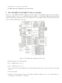
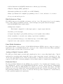
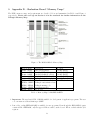
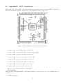
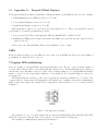
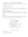
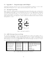
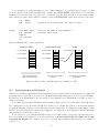
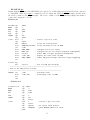
ENG364: Microcomputer Interfacing
Laboratory Manual
School of Engineering,University of Guelph
Fall 2012
Embedded computer systems, which are electronic systems that include a microcomputer to perform a
specific dedicated application, are ubiquitous. Our global economy, food production, transportation system,
military defense, communication systems, and even quality of life depend on the efficiency and effectiveness of
these embedded systems. As system engineers we play a major role in all phases of this effort: planning, design,
analysis, manufacturing, and marketing.
This document is orgainzed as follows: Section 1 introduces the main objectives, practices and recommendations for the ENG3640 laboratory. Section 2 introduces the M68HC12 microcontroller and its different
componenets. Section 3 introduces the different lab modules that will be performed by students. Section 4
gives some guidance on how to writeup the lab report. Finally, several appendices can be found at the end of
this document which are useful as a reference.
1
Laboratory Objectives and Practices
The ENG364 Microcomputer Interfacing labs are an integral part of the course. The objectives of the laboratory
are:
• to give you practical experience with the process of design and interfacing using Motorola MC68HC12.
• to help you understand and assimilate the lecture material.
• to give you practical experience with the process of design and implementation of analog/digital circuits.
• to give you hands-on-experience with microcontrollers such as the MC68HC12.
Laboratory Practices
1. Absolutely no food or drink in the laboratories.
2. Clean up after yourselves. Put paper in the recycling bin and garbage in the trash.
3. Do not leave the door or windows open.
The room will be closed after-hours if these rules cannot be followed.!
Laboratory Recommendations
• Labs are to be done in groups of at least 3 and at most 4 people.
• The labs are to be demonstrated during the lab period on the due date.
• All written lab reports are due during demonstration of the demo lab.
1
• Students are encouraged to work ahead.
• Utilize the code available in your text book!
2
The MC68HC11/MC68HC12 Microcontrollers
At the core of the 68HC12 is CPU12, a high-speed 16-bit evolution of the 68HC11 architecture that is designed
to maintain complete source-code compatibility with the 68HC11 core. The 68HC12 fully supports all internal
registers, instructions, addressing modes, and operating modes of the 68HC11. Figure 1 shows the main modules
embedded in the MCU12 Microcontroller.
Figure 1: The MCU12 Block Diagram and Modules
Additional features and benefits include:
• Up to 8 MHz bus speed at 5 V
• Up to 5 MHz bus speed at 3 V
• 64 new instructions, 20-bit Arithmetic Logic Unit (ALU), instruction queue, and 7 new indexed addressing
modes
• 16-bit data paths
• 64 Kbytes of linear and paged memory addressing capability, enabling access to more than 4 Mbytes of
program space and 1 Mbyte of data space
2
• Call and Return from Call (RTC) instructions for efficient paged addressing
• High-level Language (HLL) optimization
• Fast math capabilities (16 x 16 MUL, 32 w 16 DIV, EMACS)
• Fuzzy logic instructions for simplified programming, reduced code size, and faster code execution
• Low-power wait and stop modes
High Performance Timer
The 68HC12 timer provides flexibility, performance, and ease of use. The system is based on a free-running,
16-bit counter with a programmable prescaler, overflow interrupt, and separate function interrupts.
Additional M68HC12 timer features include:
• Multiple timer channels
– Each channel configurable for either input capture or output compare functions
• Real-time periodic interrupts
• Computer Operating Properly (COP) watchdog protection against software failures
• Pulse accumulator for external event counting or gated time accumulation
• An optional PWM offering up to four channels and up to 16-bit PWM outputs
• Optional event counter system for advanced timing operations
Pulse-Width Modulation
The 68HC12 Family offers a selection of Pulse-Width Modulation (PWM) options to support a variety of
applications. Up to four PWM channels can be selected to create continuous waveforms with programmable
rates and software selectable duty cycles from 0 to 100%.
Analog-to-Digital Converter (ADC)
The ADC periodically samples external analog signals and produces corresponding digital values. Typical
applications are measuring analog inputs like battery voltage, temperature, pressure, and fluid levels. Linear successive approximation 8-bit or 10-bit resolution Single or continuous conversion modes Multiple result
registers Selectable ADC clock Analog multiplexor allows variable number of channels with a single ADC.
Evaluation Board
The Dragon12-Plus2 Evaluation Board (EVB) is an economical tool for designing and debugging code for,
and evaluating the operation of, the MC9S12DG256CVPE microcontroller. By providing the essential MCU
timing and I/O circuitry, the EVB simplifies user evaluation of prototype hardware and software. The EVB
features a prototype area, which allows custom interfacing with the microcontroller’s I/O and bus lines. The
Dragon12-Plus2 evaluatin board can also accommodate various types and configurations of external memory
to suit a particular application’s requirements.
3
Figure 2: The Dragon12-Plus2 Evaluation Board
3
Laboratory Assignments
The course labs are structured as seven assignments. They cover the following material:
• lab0: Introduction to lab equipment and M68HC12.
• lab1: Introduction to Assembly Language Programming.
• lab2: Parallel Port Programming.
• lab3: Keypad and Switch Debouncing.
• lab4: Servo motor control and LCD interfacing.
• lab5: A/D converter and High-Tech Etch-a-sketch module.
• lab6: Interrupt Driven I/O.
• lab7: Serial RF-Communications.
These labs will expose you to a range of design activities, tool functionalities and implementation technologies.
Each lab has a set of deliverables. These typically include the circuit schematics, demonstration of the hardware
implementation and a complete report.
Due Dates
There will be seven labs throughout the term. The following are the due dates.
Item
Lab #0
Lab #1
Lab #2
Lab #3
Lab #4
Lab #5
Lab #6
Lab #7
Takes Place
Fri (Week #2)
Fri (Week #3)
Fri (Week #4)
Fri (Week #5)
Fri (Week #6)
Fri (Week #8)
Fri (Week #9)
Fri (Week #10)
Due Date
Fri (Week
Fri (Week
Fri (Week
Fri (Week
Fri (Week
Fri (Week
Fri (Week
#4)
#5)
#6)
#8)
#9)
#10)
#11)
4
Topic
Equipment used in the Lab
Introduction to MC68HC12 Controller
Parallel Port Programming
Keypad & Switch Debouncing
Servo Motor Control/LCD Interface
High-Tech Etch-a-sketch
Interrupt Driven I/O
Serial RF-Communication
4
Demonstration & Writeup
Demonstration
Be prepared to:
• demonstrate the operation of the system
• explain how your design works
• explain how the components of the system works
• answer questions related to your design.
Writeup
1. Problem Statement.
(a) Briefly summarize the problem solved in the lab.
2. Assumptions and Constraints
3. System Overview & Justification of Design
(a) Give an overview of the system to be designed.
(b) Briefly explain how the system works and reasons behind the design.
4. Hardware
(a) brief explanation of the hardware.
(b) for each component give a brief overview, pinout, pin description as required.
(c) any required calculations for hardware components (i.e Resistor values, e.t.c).
(d) complete wiring diagram for the system (multiple if necessary).
(e) timing diagram if necessary.
5. Software
(a) explain the function of your developed software, including subroutines.
(b) software flowcharts as necessary.
(c) any requierd calculations for software components (i.e., delay loops).
6. System Manual
(a) give a brief user’s manual for the system.
(b) include information as required on how to start the program, required user input, how to interpret
results.
7. Error Analysis
(a) describe any problems with the system.
(b) if no problems in the final system, describe problems/errors encountered during the development
and how they were resolved.
8. Performance Analysis
5
(a) assess performance of the system (how optimized it currently is, how fast it is, e.t.c).
(b) suggest any desired improvements.
9. Appendix
(a) include all your code with comments.
(b) other relevant material as required.
5
Academic Misconduct
The policy for this course is zero tolerance for any form of academic misconduct. Consultation with other
students is encouraged especially on design issues. However, directly copying another student’s work or copying
portions of code for example assembly language code) is an honor code violation and will result in a failing
grade and may result in a failing grade in the course. Students will automatically be refered to the Director of
the School and Dean of the college for action. Please refer to the regulations outlined in the student
handbook regarding academic misconduct.
6
6
Appendix A – D-Bug12 Commands
An HCS12 demo board may have its micro-controller programmed with the D-Bug12 monitor to support debug
activities. The D-Bug12 monitor occupies the flash memory and supports a set of debug commands. The
user can use these commands to display and modify register and memory contents, set breakpoints at certain
locations, step through the program, and download the program onto the demo board for execution. Please
refer to Chapter 3, Section 3.2 “Development Tools for the HCS12” for detailed explanation of the commands
listed below in the table.
Command
ASM < address >
BAUD < BAU DRate >
BF < StartAddress >< EndAddress > [< Data >]
BR [< Address >< Address > ..]
BULK
CALL [< Address >]
G [< Address >]
GT < address >
Description
Single line assembler/disassembler
Set the SCI communication baud rate
Block Fill user memory with data
Set/display user breakpoints
Bulk erase on-chip EEPROM
Execute a user subroutine; return to D-Bug12
Go – begin execution of user program
Go Till – set a temp breakpoint and begin
execution of user program
Display D-Bug12 command set and command syntax
Load user program in S-record format
Memory Display - display memory contents
Memory Display Word - display memory contents
Memory Modify - interactively change memory
Memory Modify Word - Change Memory Contents
Move a block of memory
Remove individual user breakpoint
Register Display – display the CPU registers
Register Modify – examine/change CPU Regs
Trace – execute an instruction, disassemble
it and display the CPU registers
Display memory contents in S-Record format
Verify memory contents against S-Record Data
HELP
LOAD [< AddressOf f est >]
MD < StartAddress > [< EndAddress >]
MDW < StartAddress > [< EndAddress >]
MM < Address > [< data >]
MMW < Address > [< data >]
MOVE < StartAdd >< EndAdd >< DestAdd >
NOBR [< Address >< Address > ..]
RD
RM
T [< Count >]
UPLOAD < StartAddress >< EndAddress >
VERF [< AddressOf f set >]
Table 1: D-Bug12 Command Set Summary
7
7
Appendix B – D-Bug12 Commands Examples
Examples of using the D-Bug12 Commands are illustrated in your text book Section 3.5.3
MD “Memory Display”
The Memory Display command is used to display memory contents
syntax
MD <StartAddress>
The following example will display the contents of memory starting at 1000.
> MD 1000
1000 00 00 00 00 00 00 00 00 00 00 00 00 00 00 ....
RM “Register Modify”
The Register Modify command is used to examine and/or modify the contents of the CPU12 registers interactively
syntax The following example will display the contents of registers
> RM
PC = 0000 1500
SP = 0A00
...
PC =1500
>
BF “Block Fill”
The Block Fill command is used to place a single 8-bit value into a range of memory locations.
syntax
BF <StartAddress> <EndAddress> [<Data>]
The following example will fill memory from location 4000 to 4100 with zeros.
> BF 4000 4100 0
CALL “Call Subroutine”
The CALL command is used to execute a subroutine and return to the D-Bug12 monitor program when the
final RTS of the subroutine is executed. When control is returned to D-Bug12, the CPU register contents are
displayed.
syntax
CALL
[<Address>]
The following example will illustrate the CALL operation.
> CALL 820
Subroutine Call Returned
PC
0820
>
SP
0A00
X
057C
Y
0000
D = A:B
0F:F9
CCR= SXHI NZVC
1001 0000
8
BR “Breakpoint Set”
The BR command is used to set a software breakpoint at a specified address or to display any previously set
breakpoints. The function of a breakpoint is to halt user program execution when the program reaches the
breakpoint address. When a breakpoint address is encountered, D-Bug12 disassembles the instruction at the
breakpoint address, prints the CPU12’s register contents, and waits for a D-Bug12 command to be entered by
the user.
syntax
BR [<Address> <Address> ..]
The following example will illustrate the BR command.
> BR 35ec 2f80 c592
Breakpoints: 35EC 2F80 C592
> BR
Breakpoints: 35EC 2F80 C592
>
NOBR “Remove Breakpoints”
The NOBR command can be used to remove one or more previously entered breakpoints.
syntax
NOBR [<Address> <Address> ..]
The following example will illustrate the BR command.
> BR 800 810 820 830
Breakpoints: 0800 0810 0820 0830
> NOBR 810 820
Breakpoints: 0800 0830
>
T “Trace”
The Trace command is used to execute one or more user program instructions beginning at the current Program
Counter (PC) location. As each program instruction is executed, the CPU12’s register contents are displayed
and the next instruction to be executed is displayed. The following example will illustrate the Trace command.
> T
PC
0803
0803
SP
X
09FE
057C
830001
Y
0000
SUBD
D = A:B
10:00
#$0001
CCR
9
=
SXHI
1001
NZVC
0000
8
Appendix C – Using D-Bug12 Routines
The D-Bug12 monitor provides a few subroutines to support I/O operations. One can utilize these I/O routines
to facilitate program development. The D-Bug12 currently provides access to 18 different utility routines
through a table of 16-bit pointers beginning at address $EE80 as shown in Table 2. This appendix will provide
you with some information that will allow you to utilize internal D-Bug12 routines.
Please refer to Page 173, Section 4.8 in your text book “Using the D-Bug12 Functions to
Perform I/O Operations for detailed examples.
Function
far main()
getchar()
putchar()
printf()
far GetCmdLine()
far sscanhex()
isxdigit()
toupper()
isalpha()
strlen()
strcpy()
far out2hex()
far out4hex()
SetUserVector()
far WriteEEByte()
far EraseEE()
far ReadMem()
far WriteMem()
Description
Start of D-Bug12
Get a char from SCI0 or SCI1
send a char out SCI0 or SCI1
Formatted Output - binary to char
Obtain a line of input from the user
Convert and ASCII hex to binary int
Checks for membership [0..0,a..f,A..F]
Converts lower case char to upper case
Checks for membership in [a..z,A..Z]
Returns the length of a string
Copies a null terminated string
Displays 8-bit number as 2 ASCII chars
Displays 16-bit number as 4 ASCII chars
Setup user interrupt service routine
Write a data byte to on-chip EEPROM
Bulk erase on-chip EEPROM
Read data from M68HC12 memory map
Write data to M68HC12 memory map
Vector Table Address
$EE80
$EE84
$EE86
$EE88
$EE8A
$EE8E
$EE92
$EE94
$EE96
$EE98
$EE9A
$EE9C
$EEA0
$EEA4
$EEA6
$EEAA
$EEAE
$EEB2
Table 2: D-Bug12 Utility Routines Summary
Here are a set of rules that you can follow to utilize these utility routines:
1. Calling a function from assembly language is simple.
• First, push the parameters onto the stack in the proper order, loading the first or only
function parameter into the D Accumulator. In other words if you have two parameters or
arguments then one will be passed by the D Accumulator and the other pushed onto the stack.
• Then call the function with a JSR instruction.
• The code following the JSR instruction should remove any parameters pushed onto the stack. If a
single parameter is stacked, a PULX or PULY instruction is one of the most efficient ways to unstack
it.
2. All 8-bit and 16-bit function results are returned in the D Accumulator. Char values returned in the D
accumulator are located in the 8-bit B Accumulator.
3. Boolean function results are zero for False and non-zero values for True.
10
Example #1:
To output a single character to the control terminal SCI (i.e., screen) you can use the int putchar(int);
function whose “Pointer Address” is located at $EE86. If the control SCI’s transmit data register is full when
the function is called, putchar() will wait until the transmit data register is empty before sending the character.
Adding the following instruction sequence in your program will output the character “A” to the control
SCI:
putchar
equ
...
ldd
jsr
...
$EE86
#‘A’
[putchar,PCR]
The addressing mode used in the jsr instruction of this example is a form of indexed indirect addressing
that uses the program counter as an index register. In reality, the HCS12 does not support PCR. Instead,
the PCR mnemonic is used to instruct the assembler to calculate an offset to the address specified by the
label putchar. The MiniIDE software supports this syntax. However, if you are using an assembler that does
not support program-counter relative indexed addressing the following two instruction sequence can be used
instead:
ldx
jsr
putchar
0,x
; load the address of putchar
; call the subroutine
Important: If the name of a library function is preceded by the keyword far, then it is located in the
expanded memory and must be called by using the call instruction.
Example #2:
To retrieve a single character from the control terminal SCI use the int getchar(void); function whose pointer
address is located in “$EE84”. If an unread character is not available in the receive data register when this
function is called, it will wait until one is received. Because the character is returned as an integer, the 8-bit
character is placed in accumulator B.
Adding the following instruction sequence in your program will read a character from the SCI0 port
getchar
equ
...
jsr
...
$EE84
[getchar,PCR]
Example #3:
The following is a sample code for utilizing the getchar() and printf() utility routines Notice that there are
two org statements. The first org statement is to set the starting address of the variables and constants at
location $1000. The second org statement is to set the start address of the main program to be executed to
location $1100. When you attempt to run your program you need to issue the command g $1100 in the miniIDE
environment.
CR
LF
getchar
printf
EQU
EQU
EQU
EQU
$0D
$0A
$EE84
$EE88
;
;
;
;
ORG
$1000
; Start Address of variables/constants
11
ASCII Code
ASCII Code
Address of
Address of
for Carriage Return
for Line Feed
Debug12 Utility Function getchar()
Debug12 Utility Function printf()
msg
db
"char pressed is %c",CR,LF,0
getnewval
ORG
LDX
JSR
$1100
getchar
0,X
; Start Address of main program
; get the character from the keyboard
CMPB
BEQ
#$1B
terminate
; Check if the char is an ESC
; jump to end of program
#msg
printf
0,X
;
;
;
;
PSHD
LDD
LDX
JSR
terminate
BRA
SWI
getnewval
push char on stack (parameter for printf)
second parameter in ACC D
Load Index Reg X with printf address
print message on terminal
; repeat getting new chars
; end of program (return to D-Bug12)
12
9
Appendix D – Evaluation Board “Memory Usage”
The EVB’s memory usage and requirements are described below and summarized in Table 3 and Figure 3
respectively. Please refer to Page 94 Section 3.4 in the textbook for further information on the
D-Bug12 Memory Map.
Figure 3: The MC9S12DG256 Memory Map
Address Range
$0000 - $03FF
$0400 - $0FFF
$1000 - $3BFF
$3C00 - $3FFF
$4000 - $EE7F
$EE80 - $EEBF
$EEC0 - $EEFF
$EF00 - $EF8B
$EF8C - $EFFF
$F000 - $FFFF
Description
CPU I/O Registers
On-chip EEPROM
On-chip SRAM (For User)
On-chip SRAM (D-Bug12)
D-Bug12 Code
User Accessible func Table
D-Bug12 customization data
D-Bug12 startup code
rest/interrupt table
Bootloader
Location
on-chip (MCU)
on-chip (MCU)
on-chip (MCU)
on-chip (MCU)
on-chip Flash (MCU)
Fixed Flash
Table 3: Memory Map for M68HC12A4EVB
1. Important: The user has 11 KB of SRAM available for development of application programs. The user
code can start at address $1000 upto $3BFF
2. Part of the on-chip EEPROM (4K) is available for user programs. Even though the HCS12DX256 parts
contain 4 KB of EEPROM, only the upper 3 KB are visible, as the lower 1 KB is overlaid with the I/O
registers.
13
3. The monitor program, D-Bug12, occupies locations $4000 upto $EE7F.
Below is an example of a program that starts at memory location $1000 (On-chip RAM).
ORG
ldaa
adda
suba
staa
end
$1000
$1500
$1502
$1505
$1510
;
;
;
;
;
Starting Address of Program
A <== [$1500]
A <== [A] + [$1502]
A <== [A] - [$1505]
$1510 <== [A]
14
10
Appendix E – MCU Connections
Eight pin header connectors (H1 .. H8), surrounding the breadboard provide access to the MCU’s I/O and bus
lines as seen in Figure 4. These connectors are located adjacent to the prototype area.
Figure 4: Main Pin Headers on the Dragon12-Plus2 Board
1. Connector H1 located at upper/left of breadboard.
2. Connector H2 located at lower/left of breadboard (below H1).
3. Connector H3 located at bottom/left of breadboard.
4. Connector H4 located at bottom/right of breadboard.
5. Connector H5 located at lower/right of breadboard.
6. Connector H6 located at upper/right of breadboard.
7. Connector H7 located at top/right of breadboard.
8. Connector H8 located at top/left of breadboard.
Table 4 provides a brief description of the signals.
I/O Pin Usage
Many I/O pins of the MC9S12DG256 on the Dragon12-Plus2 board are used by on-board peripherals, here are
examples:
1. PORT A: Keypad.
15
Connector
H1
H1
H1
H2
H2
H2
H2
H3
H3
H3
H4
H4
H5
H5
H6
H6
H7
H7
H8
H8
Signal Name
PP3, PP2, PP1, PP0
PK3, PK2, PK1, PK0
PT0, PT1, PT2, PT3
PT4, PT5, PT6, PT7
PK5, PK4
PJ1, PJ0
PB0, PB1, PB2, PB3, PB4
PB5, PB6, PB7
PH7, PH6, PH5, PH4
PE7, PE6, PE5, PE4
PH3, PH2, PH1, PH0
PE3, PE2, PE1, PE0
PA0, PA1, PA2, PA3, PA4, PA5, PA6, PA7
PAD00, PAD08, PAD01, PAD09
PAD02, PAD03, PAD04, PAD05, PAD06, PAD07
PAD10, PAD11, PAD12, PAD13, PAD14, PAD15
PS0, PS1, PS2, PS3, PS4, PS5, PS6, PS7
PM6, PM7
PM0, PM1, PM2, PM3, PM4, PM5
PP4, PP5, PP6, PP7
Port
Port
Port
Port
Port
Port
Port
Port
Port
Port
Port
Port
Port
Port
Port
Port
Port
Port
Port
Port
Port
P(0..3)
K(0..3)
T(0..3)
T(4..7)
K(4..5)
J(0..1)
B(0..4)
B(5..7)
H(4..7)
E(4..7)
H(0..3)
E(0..3)
A(0..7)
AD0(0,1,8,9)
AD0(2..7)
AD1(0..5)
S(0..7)
M(6,7)
M(0..5)
P(4..7)
Description
Gen Purpose I/O
Gen Purpose I/O
NOT USED
NOT USED
Gen Purpose I/O
NOT USED
Gen Purpose I/O
Gen Purpose I/O
Gen Purpose I/O
NOT USED
Gen Purpose I/O
NOT USED
Gen Purpose I/O
Analog-to-Dig
Analog-to-Dig
Analog-to-Dig
Serial Comm
NOT USED
NOT USED
Gen Purpose I/O
Table 4: MCU Connectors J8/J9 Pin Assignments
2. PORT B: Light Emmitting Diodes (LEDs)
3. PORT H: DIP and Pushbutton Switches
4. PORT K: Liquid Crystal Display (LCD)
5. PORT P: 7-Segment Display
6. PORT AD: Light Sensor, Temp Sensor, Trimmer Pot
IMPORTANT:
Fortunetly, it’s unlikely that all on-board peripherals will be used by one application program. So the I/O pins
on unused peripheral devices can still be used by your circuits on the breadboard. For instance, if you don’t
touch the 4x4 on-board keypad, the entire port A will be available to your circuits.
16
11
Appendix F – Port Register
Each port within the M68HC12 has several registers that are used to control its functionality and also give the
status of the port following a read/write transaction. Table 5 provides a brief description of the regular I/O
ports and their associated registers. Ports A, B, E, K can be used for Input/Output based on how the “Data
Direction” register has been programmed.
Port
PORT A
PORT B
PORT P
PORT H
PORT E
PORT K
Register
PORTA
DDRA
PORTB
DDRB
PORTP
DDRP
PORTH
DDRH
PORTE
DDRE
PORTK
DDRK
Description
Data Register A
Data Direction Register
Data Register B
Data Direction Register
Data Register P
Data Direction Register
Data Register H
Data Direction Register
Data Register E
Data Direction Register
Data Register K
Data Direction Register
A
B
P
H
E
K
Address
$0000
$0002
$0001
$0003
$0258
$025A
$0260
$0262
$0008
$0009
$0032
$0033
Current Usage
Keypad
LED
7-Seg Display
DIP Switches
IRQ, XIRQ
LCD
Table 5: M68HC12 I/O Ports and Associated Registers
Table 6 provides a brief description of the I/O ports (H,J) that have interrupt capability (Wakeup). Port
P is very similar to ports H and J in functionality.
Port
PORT H
PORT J
Register
PTH
DDRH
PTIH
RDRH
PERH
PPSH
PIEH
PIFH
PTJ
DDRJ
PTIJ
RDRJ
PERJ
PPSJ
PIEJ
PIFJ
Description
Data Register H
Data Direction Register H
Input Register H
Reduced Drive Register H
Pull Devide Enable H
Polarity Select Register H
Interrupt Enable Register (Wakeup)
Interrupt Flag Register H
Data Register J
Data Direction Register J
Input Register J
Reduced Drive Register J
Pull Device Enable J
Polarity Select Register J
Interrupt Enable Register J
Interrupt Flag Register J
Address
$0260
$0262
$0261
$0263
$0264
$0265
$0266
$0267
$0268
$026a
$0269
$026b
$026c
$026d
$026e
$026f
Table 6: I/O Ports with Interrupt Enable Capability
17
Table 7 provides a brief description of other I/O ports and registers that are used for “Real Time Interrupt” (Section 6.7 in Text Book), “Analog-to-Digital Conversion” (Section 12.3 in Text Book), and “Serial
Communication”.
Port
RTI
PORT ATD
PORT SCI 0
Register
RTICTL
CRGFLG
CRGINT
ATD0CTL0
ATD0CTL1
ATD0CTL2
ATD0CTL3
ATD0CTL4
ATD0CTL5
ATDSTAT0
ATDSTAT1
PORTAD0
ATD0DR0H
ATD0DR7H
SCI0BDH
SCI0BDL
SCI0CR1
SCI0CR2
SCI0SR1
SCI0SR2
SCI0DRH
SCI0DRL
Description
Real Time Interrupt Control Register (RTR0:RTR6)
The CRG Flag Register (RTIF)
The CRG Interrupt Enable Register (RTIE)
Control Register 0 (Reserved)
Control Register 1 (Reserved)
Control Register 2 (ADPU)
Control Register 3 (S8C, S4C, S2C, S1C)
Control Register 4 (PRS4:PRS0)
Control Register 5 (SCAN, MULT, CC, CB, CA)
Status Register 0 (SCF)
Status Register 1 (Reserved)
Data Input (Bit7:Bit0)
Result Register 0 (High Byte)
Result Register 7 (High Byte)
Baud Rate Register High
Baud Rate Register Low
Control Register 1
Control Register 2
Status Register 1
Status Register 2
Data Register High
Data Register Low
Table 7: M68HC12 Ports and Registers
18
Address
$003B
$0037
$0038
$0080
$0081
$0082
$0083
$0084
$0085
$0086
$0087
$008F
$0090
$009E
$00C8
$00C9
$00CA
$00CB
$00CC
$00CD
$00CE
$00CF
12
Appendix G – Dragon12-Plus2 Displays
The Dragon12-Plus2 Board has several means to display information by the MCU12. Here are some examples:
1. Light Emmitting Diodes, (LEDs) (connected to Port B)
2. Seven-Segment Displays, (connected to Port P)
3. Liquid Crystal Display, (connected to Port K).
Each peripheral is connected to a specific port as demonstrated above. These ports can still be used as
general purpose ports if the peripherals are not used.
1. If you don’t use the LCD or just unplug the LCD, the Port K will be available as well.
2. Port B drives LEDs, but if you ignore the status of the LEDs, the port B can drive any other I/O devices
on the breadboard.
Please refer to the “Dragon12-Plus2 Trainer, User’s Manual” for more details.
LEDs:
Each port B line is monitored by an LED. In order to turn on port B LEDs, the PJ1 (port J pin 1) must be
programmed as output and set for logic zero.
7-Segment LED multiplexing
There are 4 digits of 7-Segment LEDs on the Dragon12-Plus2 board. The type of the 7-Segment display on
board is called common cathode. in an individual digit, all anodes are driven individually by an output pot
and all cathodes are internally connected together. Before sending a number to a 7-Segment LED, the number
must be converted to its corresponding 7-segment code depending how the 7-segment display is connected to
an output port.
The Dragon12-Plus2 board uses port B to drive 7-segment anodes and used PP0-PP3 (i.e., Port P) to drive
common cathodes. In the next few paragraphs we will explain how to multiplex 7-segment by displaying the
number 1234 on the display. By convention, the 7-Segments are called segment a, b, c, d, e, f and g, as shown
in Figure 5.
Figure 5: The Dragon12 7-Segment
The segment a, b, c, d, e, f, g and Decimal Point are driven by (PORT B) PB0, PB1, PB2, PB3, PB4, PB5,
PB6, PB7, respectively. The hex value of the segment code is shown in the following table:
The schematic for multiplexing 4 digits is shown in Figure 7.
19
Figure 6: Hex Value of the numbers ‘1, 2,3, 4’
Figure 7: Multiplexing the 7-Segment Displays on the Dragon12-Plus2 Board
The digits 3, 2, 1 and 0 are driven by PP0, PP1, PP2 and PP3, respectively (PORT P). The 7-Segment
LED is turned on one at a time at 250 HZ refresh rate. It’s so fast that our eyes will perceive that all digits
are turned on at the same time. To display the number ‘1234’ on the 7-Segment display, the following steps
should be taken:
1. Output $06 to Port B, set PP0 low and PP1, PP2 and PP3 high. The number 1 is shown on the digit 3
(the leftmost digit) but other 3 digits are turned off.
2. Delay 1ms.
3. Output $5B to Port B, set PP1 low and PP0, PP2 and PP3 high. The number 2 is shown on the digit 2
but other 3 digits are turned off.
4. Delay 1ms.
5. Output $4F to Port B, set PP2 low and PP0, PP1 and PP3 high. The number 3 is shown on the digit 1
but other 3 digits are turned off.
6. Delay 1ms.
7. Output $66 to Port B, set PP3 low and PP0, PP1 and PP2 high. The number 4 is shown on the digit 0
(the rightmost digit) but other 3 digits are turned off.
8. Delay 1ms.
9. Go back to step 1.
20
13
Appendix H – Dragon12-Plus2 Keypad and DIP Switches
The Dragon12-Plus2 Board has several means to send information to the MCU12. Here are some examples:
1. Hex Key Pad, (connected to Port A)
2. DIP Switches, (connected to Port H)
3. Push Buttons, (connected to Port H)
Each peripheral is connected to a specific port as demonstrated above. These ports can still be used as
general purpose ports if the peripherals are not used. Please refer to the “Dragon12-Plus2 Trainer, User’s
Manual” for more details.
DIP Switch and Pushbuttons:
Port H is connected to an 8-position DIP switch. The DIP switch is connected to VCC via the RN4 (four
2.7K resistors) and RN5 (four 2.7K resistors). When Port H is programmed as an output port, the DIP switch
setting is ignored.
Keypad:
Port A is an 8-bit bi-directional port. Its primary usage is for a 4x4 keypad. If the port is not used for the
keypad, it can be used as a general purpose I/O. The Dragon12-Plus2 board uses port A to scan and test if a
key has been pressed. The schematic for the keypad connection is shown in Figure 8.
Figure 8: The Dragon12 Keypad
Keypad Connections:
• PA0 connects COL0 of the keypad.
• PA1 connects COL1 of the keypad.
21
• PA2 connects COL2 of the keypad.
• PA3 connects COL3 of the keypad.
• PA4 connects ROW0 of the keypad.
• PA5 connects ROW1 of the keypad.
• PA6 connects ROW2 of the keypad.
• PA7 connects ROW3 of the keypad.
The following explains how to scan and test if a specific key has been pressed on the keypad.
1. Keypad scan routine sets PA3 low and PA0, PA1, PA2 high, then tests PA4-PA7.
• If no key is pressed, PA4-PA7 remain high.
• If PA7 = low, the key 15 (D) is pressed.
• if PA6 = low, the key 11 (C) is pressed.
• If PA5 = low, the key 7 (B) is pressed.
• If PA4 = low, the key 3 (A) is pressed.
2. Keypad scan routine sets PA2 low and PA0, PA1, PA3 high, then tests PA4-PA7.
• If no key is pressed, PA4-PA7 remain high.
• If PA7 = low, the key 14 (#) is pressed.
• if PA6 = low, the key 10 (9) is pressed.
• If PA5 = low, the key 6 (6) is pressed.
• If PA4 = low, the key 2 (3) is pressed.
3. Keypad scan routine sets PA1 low and PA0, PA2, PA2 high, then tests PA4-PA7.
• If no key is pressed, PA4-PA7 remain high.
• If PA7 = low, the key 13 (0) is pressed.
• if PA6 = low, the key 9 (8) is pressed.
• If PA5 = low, the key 5 (5) is pressed.
• If PA4 = low, the key 1 (2) is pressed.
4. Keypad scan routine sets PA0 low and PA1, PA2, PA3 high, then tests PA4-PA7.
• If no key is pressed, PA4-PA7 remain high.
• If PA7 = low, the key 12 (*) is pressed.
• if PA6 = low, the key 8 (7) is pressed.
• If PA5 = low, the key 4 (4) is pressed.
• If PA4 = low, the key 0 (1) is pressed.
22
14
Appendix I – S-Record Format
The S-Record format for output modules was devised for the purpose of encoding programs or data files in a
printable format for transportation between computer systems.
14.1
S-Record Content
S-Records are essentially character strings made of several fields that identify the recored type, record length,
memory address, code/data, and checksum. Each byte of binary data is encoded as a 2-character hexadecimal
number. The 5 fields that comprise an S-record are shown below
The S-Record fields are composed as follows:
Type
Record Length
Address
Code/Data
CheckSum
1. Type Field: 2 characters, Contents: S-Record types, S0, S1, e.t.c
2. Record length Field: 2 characters, Contents: the count of the character pairs in the record
3. Address Field: 4,6, or 8 characters, Contents: the 2-,3-,or 4-byte address at which the data field is to
be loaded into memory.
4. Code/data Field: 0-2n characters, Contents: from 0 to n bytes of executable code, memory-loadable
data, or descriptive information.
5. Checksum: 2 characters, Contents: The least significant byte of the 1’s complement of the sum of the
values represented by the pairs of characters making up the record length, address, and the code/data
fields.
14.2
S-Record Types
Eight types of S-records have been defined to accomodate the several needs of the encoding, transportation,
and decoding functions. Table 8 describes the different S-records types.
Type
S0
S1
S9
Description
The header record for each block os S-records.
A record containing code/data
A termination record for a block of S1 records.
Table 8: S-Record Types
14.3
S-Record Example
Shown below is a typical S-record format module, as printed or displayed:
S0030000FC
S10B08008604C605180620FE5B
S9030000FC
--> 03 indicates 3 char pairs follow.
The above module consists of an S0 header record, one S1 code/data record, and an S9 termination record.
23
15
Appendix J – Using Interrupts with D-Bug12
An interrupt is a hardware solution for both even detection and changing the program flow to a service routine.
When using an interrupt, the service routine is called the interrupt service routine or ISR.
15.1
Interrupt Program Flow
Figure 9 shows the overall program flow in an interrupt driven system. The main program, or background, is
shown running an endless task loop. Once an interrupt event is detected, the background will be interrupted
and the CPU will automatically jump to and execute the interrupt service routine. This is like a subroutine call
instruction that is initiated by a hardware event. The interrupt service routine ends with an “rti” instruction,
which returns the CPU to the background to resume execution at the instruction that would have run if the
interrupt had not occurred.
Background
Foreground
main
ISR
INT
Initialize
Service Event
or Set Flag
Background
Tasks
rti
Figure 9: Interrupt Program Flow
15.2
68HC12 Interrupt Sources and Setup
We can divide the interrupt sources into four groups: interrupts from on-chip resources (Timers, A/D, ..),
external interrupts (IRQ,XIRQ, ..) software interrupts (SWI, ..) and reset exceptions. An interrupt vector is
two fixed memory locations that contain the address of the interrupt service routine for a given interrupt. The
CPU12 interrupt vectors are stored at $FF80-$FFFF. Table 9 shows the interrupt sources and vector location
for some interrupt sources on the M68HC12.
Interrupt Source
Analog to Digital Conv
SCI 1 Serial System
SCI 0 Serial System
SPI Serial System
Timer Channel 7
Timer Channel 0
Real Time Interrupt
IRQ
Vector Address
$FFD2:$FFD3
$FFD4:$FFD5
$FFD6:$FFD7
$FFD8:$FFD9
$FFE0:$FFE1
$FFEE:$FFEF
$FFF0:$FFF1
$FFF2:$FFF3
CCR Mask
I
I
I
I
I
I
I
I
Local Enables
ATD0CTL2(ASCIE)
SC1CR2(TIE, TCIE, RIE, ILIE)
SC0CR2(TIE, TCIE, RIE, ILIE)
SP0CR1(SPIE,SPTIE)
TIE(C7I)
TIE(C0I)
CRGINT(RTIE)
IRQCR(IRQEN)
Table 9: 68HC12 Interrupt Sources & Vector Addresses
24
So, for example, to load the interrupt vector for “Timer Channel 0”, we would use the following code: This
loads the address of the Ic0Isr interrupt service routine into $FFEE:$FFEF, which is the vector for Timer
Channel 0. Now when a rising edge is detected on PORTT, bit 0, the CPU saves the context, sets the I mask,
and loads the program counter with the contents of address $FFEE:$FFEF, which is the address of the ISR.
Ic0Isr
org
FDB
....
....
movb
ldd
addd
std
rti
$FFEE
Ic0Isr
; Ic0Isr is the location where the ISR is located
#C0F, TFLG1
PulseCnt
#1
PulseCnt
; Ic0Isr is the ISR for Timer Channel 0
; increment pulse count
Figure 10 illustrates the concept graphically.
ROM VECTORS
VTC2: 0xFFEA
VTC1: 0xFFEC
VTC0: 0xFFEE
0B
2A
0B
2C
0B
2E
RAM JUMP TABLE
JTC2: 0x0B2A
JTC1: 0x0B2C
JTC1: 0x0B2E
00
00
00
00
71
00
RAM
TC0−ISR 0x7100 1st Inst
0x7100
RTI
Specified by Motorola’s
68HC12 System Designer
Specified by the D−Bug12
Monitor
Specified by the application
Programmer
Figure 10: Memory Map of the Interrupt Vector Linkage for TC2
15.3
Using Interrupts with D-Bug12
When we are writing programs that use interrupts under the D-bug12 monitor, it is impractical to change the
actual interrupt vectors. The vectors are stored in ROM with D-Bug12 and some vectors are used by D-Bug12.
Even if they are in Flash ROM, it is not practical to reprogram the whole Flash ROM every time we write or
change a program.
To accommodate interrupts, D-Bug12 includes a utility routine, SetUserVec(), that will load the ISR address
into a jump table located in monitor RAM. The actual vector contains the address of an interrupt dispatch
program in D-Bug12. If there is a user ISR address in the jump table, the dispatch program jumps to that
address. If no user ISR address exists in the jump table, the dispatch program displays a message indicating
that an unexpected interrupt occurred.
To use SetUserVec(), we pass the ISR address and a vector number that corresponds to the interrupt source.
The vector numbers for SetUserVec() are shown in Table 10 (Please check Page 273 Table 6.3 in your
text book for details). For example, if we need to use the Timer Channel 0 interrupt, the vector number
would be 55.
25
Interrupt Source
PORTH Key Wake-up
PORTJ Key Wake-up
A-to-D1
A-to-D0
SCI#1
SCI#0
SPI#0
Pulse Accum. Edge
Pulse Accum. Overflow
Timer Overflow
Timer Channel 7 .. Timer Channel 0
RTI
IRQ
XIRQ
SWI
Unimplemented Opcode Trap
Ram Vec Address
$3E4C
$3E4E
$3E50
$3E52
$3E54
$3E56
$3E58
$3E5A
$3E5C
$3E5E
$3E60 ..$3E6E
$3E70
$3E72
$3E74
$3E76
$3E78
Vec Number
38
39
40
41
42
43
44
45
46
47
48 .. 55
56
57
58
59
60
Table 10: SetUserVec() Interrupt Vector Numbers
EXAMPLE #1:
It is very simple to set up the SRAM interrupt vector. Assuming that the service routine for the IRQ interrupt
starts with the label irqISR. Recall that the RAM Vector Address of the IRQ is $3E72. Then one of the
following three methods can be used to establish the SRAM table entry for the IRQ inteterrupt:
Method #1
org
dc.w
$3E72
irqISR
Method #2
ldd
std
#irqISR
$3E72
Method #3
setuservector
equ
ldd
pshd
ldab
clra
ldx
jsr
puld
$EEA4
#irqISR
#57
setuservector
0,x
; address of Debug-12 utility function
; push irqISR address on stack
;
; load vector number of IRQ
;
;
; clean up the stack
26
EXAMPLE #2:
Assume that the IRQ pin of the HCS12DP256 is connected to a 1-Hz digital waveform and Port B is connected
to eight LEDs. Write a program to configure Port B for output and enable the IRQ interrupt, and also write
the service routine for the IRQ interrupt. The service routine for the IRQ interrupt simply increments a
counter and outputs it to Port B.
Solution #1
UserIRQ
DDRB
DDRJ
PTJ
PTB
IRQCR
equ
$3E72
equ
3
equ
$26a
equ
$268
equ
1
equ
$1e
org
$1000
count
ds.b
1
; reserve 1 byte for count
org
$1500
lds
#$1500
; set up the stack pointer
movw
#IRQISR,UserIRQ ; set up interrupt vector in SRAM
clr
count
movb
#$FF,DDRB
; configure Port B for output
bset
DDRJ,$02
; configure PJ1 pin for output (required in Dragon12)
bclr
PTJ,$02
; enable LEDs to light (required in Dragon12)
movb
count,PTB
; display the count value on LEDs
movb
#$C0,IRQCR
; enable IRQ pin interrupt and select edge-triggering
cli
; "
forever nop
bra
forever
; wait for IRQ pin interrupt
; ------------------------------------------------------------; This is the IRQ service routine.
; ------------------------------------------------------------IRQISR inc
count
; increment count
movb
count,PTB
; and display count on LEDs
rti
end
Solution #2
setuservector
DDRB
DDRJ
PTJ
PTB
IRQCR
count
equ $3E72
equ
3
equ
$26a
equ
$268
equ
1
equ
$1e
org
$1000
ds.b
1
org
$1500
lds
#$1500
ldd
#IRQISR
pshd
; reserve 1 byte for count
; set up the stack pointer
; push IRQISR address on stack
;
27
ldab
#57
; load vector number of IRQ
clra
;
ldx setuservector ; Start calling setuservector
jsr
0,x
;
puld
; clean up the stack
clr
count
movb
#$FF,DDRB ; configure Port B for output
bset
DDRJ,$02
; configure PJ1 pin for output (required in Dragon12)
bclr
PTJ,$02
; enable LEDs to light (required in Dragon12)
movb
count,PTB ; display the count value on LEDs
movb
#$C0,IRQCR ; enable IRQ pin interrupt and select edge-triggering
cli
; "
forever
nop
bra
forever
; wait for IRQ pin interrupt
; ----------------------------------------------------------------------------------------------; This is the IRQ service routine.
; ----------------------------------------------------------------------------------------------IRQISR
inc count
; increment count
movb count,PTB ; and display count on LEDs
rti
end
28
EXAMPLE #3:
The following is yet another example of implementing an ISR with D-Bug12.
*************************************************************************
** Example: a program that uses the output compare function of timer
**
channel 7 (TC7) to create time delays.
** Assumptions: E-clock = 8MHz
** Functionality: The program performs 40 output compare operations on
**
the TC7 with each operation creating 25 ms delay.
**
Forty such operations will create a delay of one second
*************************************************************************
CR
equ
$0D
; ASCII code of carriage return
LF
equ
$0A
; ASCII code of line feed
tios
equ
$40
; timer IC/OC select register
tcnt
equ
$44
; timer count register
tscr1
equ
$46
; timer system control register
tctl1
equ
$48
; timer control register 1
TIE
equ
$4C
; timer mask register 1
TSCR2
equ
$4D
; timer mask register 2
tflg1
equ
$4E
; timer flag register 1
tc7
equ
$5E
; timer output compare register 7
pactl
equ
$60
; pulse accumulator control register
printf
equ
$EE88
setuservector
equ
$EEA4
oc7_int_vect
oc7_vec_num
equ
equ
$FFE0
48
oc7_cnt
org
rmb
$1000
1
seconds
rmb
1
total
rmb
1
org
lds
clr
jsr
ldaa
staa
$1100
#$2000
seconds
init_oc7
#10
total
;
;
;
;
memory location to hold the
starting address of printf()
memory location to hold the
starting address of SetUserVector()
;
;
;
;
;
;
start address of variables
number of output compare ops
remained to be performed
number of seconds passed
since the beginning
number of seconds remained
;
;
;
;
;
starting address of the program
initialize the stack pointer
start from 0 seconds
initialize oc7 parameters
store 10 in total
; the following 6 instructions set up oc7 interrupt vector
ldd
#oc7_isr
pshd
; push oc7_isr address on stack
ldab
#oc7_vec_num
; load vector number of oc7
clra
ldx
setuservector
; setup D-bug12 for ISR
29
jsr
puld
0,x
; clean up the stack
; the following two instructions enable oc7 interrupt
bset
TIE,$80
; enable oc7 interrupt
cli
; enable interrupt globally
; the outer loop make sure 10 second delays are created
outer_loop
tst
total
beq
done
movb
#40,oc7_cnt
; set up the number of oc7 compares
; to be performed
ldd
#25000
std
tc7
; initialize tc7 to 25000 so that every
; creates 25 ms delay
; *********************************************************************
; the inner loop performs 40 oc7 output compare operations
; to create 1 second delay with each operation creates
; 25 milliseconds delay
; *********************************************************************
inner_loop
tst
oc7_cnt
; wait for 40 oc7 operations to
; be performed
bne
inner_loop
; and oc7 interrupt will occur here
inc
seconds
; one second delay has been created
clra
ldab
seconds
pshd
ldd
#time_msg
ldx
printf
jsr
0,x
; print out the message
leas
2,sp
dec
total
jmp
outer_loop
done
swi
; **********************************************************************
; the following subroutine initializes the oc7 parameters
; **********************************************************************
init_oc7
movb
#$80,tscr1
; enable timer, timer runs during wait state,
; and while in background mode,
; also clear flags normally
clr
TIE
; disable all output compare interrupts
movb
#$80,tios
; select channel 7 to act as
; output compare
movb
#$2B,TSCR2
; set the timer counter prescale factor
; to 8 and reset tcnt on a successful
; output compare 7 event
movb
#$00,pactl
; choose timer prescaler clock as
; timer counter clock
30
rts
; *********************************************************************
; oc7 interrupt service routine
; *********************************************************************
oc7_isr
bclr
tflg1,$7F
; clear c7F flag
dec
oc7_cnt
rti
time_msg
db
end
" %d seconds have passed",CR,LF,0
31