1
Freescale Semiconductor
Application Note
Document Number: AN3098
Rev. 0, 11/2006
MSC8144 PCI Example Software
by
Barbara Johnson
NCSD DSP Applications
Freescale Semiconductor, Inc.
Austin, TX
In a PCI system, auto-configuration software offers ease of
use for the system user by automatically configuring PCI
add-in cards at power-on. This application note provides
example software for use by a PCI host to configure the
MSC8144 DSP as a PCI agent. This device configuration is
required before any PCI transactions can occur between the
host and the MSC8144.
1
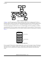
PCI Basics
Peripheral component interconnect (PCI) is a standard that
provides an interconnect mechanism between peripheral
components, add-on devices, and memory subsystems.
Developed by Intel, PCI is widely used in modern PCs to
provide a way of adding peripherals such as video cards,
sound cards, and network adapters on the same bus that is
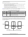
used to communicate with the CPU. Figure 1 shows an
example PCI-based system. The CPU connects to the
primary PCI bus on a PCI host bridge that translates between
CPU bus cycles and PCI bus cycles. The PCI-PCI bridge
connects the primary PCI bus to the secondary PCI bus.
Electrical loading issues limit the number of devices that a
single PCI bus can support, so PCI-PCI bridges are often
used to allow the system to support more PCI devices. To
support older, legacy devices, some PCs use a PCI-ISA
bridge for connecting to the PCI bus.
© Freescale Semiconductor, Inc., 2006. All rights reserved.
Contents
1 PCI Basics . . . . . . . . . . . . . . . . . . . . . . . . . . . . . . . . . . .1
2 MSC8144 PCI Controller . . . . . . . . . . . . . . . . . . . . . . .3
3 Hardware Requirements and Setup . . . . . . . . . . . . . . . .3
3.1 Requirements . . . . . . . . . . . . . . . . . . . . . . . . . . . . .3
3.2 Switch Settings . . . . . . . . . . . . . . . . . . . . . . . . . . . .4
3.3 Board Control and Status Register Setting . . . . . . .4
4 PCI Device Detection Example . . . . . . . . . . . . . . . . . .4
5 Memory Allocation Example . . . . . . . . . . . . . . . . . . . .7
6 MSC8144 Inbound Configuration Example . . . . . . . . .9
7 MSC8144 CCSR Mapping Example . . . . . . . . . . . . .11
8 MSC8144 Outbound Configuration Example . . . . . . 13
9 Cache Line Size . . . . . . . . . . . . . . . . . . . . . . . . . . . . .15
10 Latency Timer . . . . . . . . . . . . . . . . . . . . . . . . . . . . . . 15
11 Interrupt Handling . . . . . . . . . . . . . . . . . . . . . . . . . . . .16
12 MPC8560 Host Configuration Code . . . . . . . . . . . . . .16
13 MPC8560 Header File . . . . . . . . . . . . . . . . . . . . . . . .22
PCI Basics
CPU
Memory
PCI Host
Bridge
PCI Bus 0
PCI-ISA
Bridge
Network
Adapter
PCI-PCI
Bridge
ISA Bus
Video
PCI Bus 1
I/O
Controller
SCSI
Figure 1. Example PCI System
In Figure 1, the CPU operates as the PCI host. In the host mode, the CPU configures the PCI devices
attached to the bus. Because PCI uses a shared bus topology, there must be an arbitration scheme to grant
bus mastership to the requesting PCI device. Arbitration is handled by the host or an external arbiter.
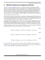
From the host perspective, the PCI devices are accessible through a read-write mechanism. An address
space dedicated for PCI use contains a memory range for each PCI device on the bus. The host accesses
the PCI devices by performing reads or writes to specific addresses in the PCI memory space, as shown in
Figure 2.
Host View
Device x
PCI memory
Device y
Program
Main memory
Data
Figure 2. Example Host View
Devices on the PCI bus must be configured before they can be used. For example, when a PC first boots
up, each PCI device is assigned a region of PCI address space so that it becomes accessible to the CPU.
After the devices are initialized, they respond to transactions that fall within their allocated memory
ranges.
MSC8144 PCI Example Software, Rev. 0
2
Freescale Semiconductor
MSC8144 PCI Controller
2
MSC8144 PCI Controller
The MSC8144 PCI controller complies with the PCI Local Bus Specification, Revision 2.2. It operates in
agent mode and can act as initiator (master) or target (slave) device. It uses a 32-bit multiplexed
address/data bus that operates at frequencies up to 66 MHz. Features of the PCI controller are as follows:
• 32-bit PCI interface
• Up to 66 MHz operation
• Agent mode
• Accesses to all PCI address spaces
• 64-bit dual-address cycles (as a target only)
• Internal configuration registers accessible from PCI and internal buses
• Contains L2 ICache-line (32 byte) buffers to allow PCI-to-memory and memory-to-PCI streaming
• Memory prefetching of PCI read accesses and support for delayed read transactions
• Posting of processor-to-PCI and PCI-to-memory writes
• Inbound and outbound address translation units for address mapping between PCI and local busses
• Supports parity
• PCI 3.3-V compatible
3
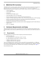
Hardware Requirements and Setup
All tests described in this document were performed on the MSC8144 application development system
(MSC8144ADS), which consists of an MPC8560 host processor that connects to the MSC8144 on the PCI
bus.
3.1
Requirements
The following items are required to run the examples presented in this document:
• MSC8144ADS board
• PC with CodeWarrior™ for StarCore version 3.2 or later
• PC with CodeWarrior for PowerPC™ version 8.7 or later
• USBTap for MSC8144 OCE connection
• USBTap for MPC8560 COP connection
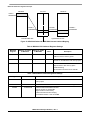
Two sets of debugger tools are required to connect to the MSC8144 and the MPC8560. A USBTap for
OCE connects the MSC8144 to the CodeWarrior for StarCore tools through JTAG. Similarly, a USBTap
for COP connects the MPC8560 to the CodeWarrior for PowerQUICC tools through JTAG. Figure 3
shows the hardware setup.
MSC8144 PCI Example Software, Rev. 0
Freescale Semiconductor
3
PCI Device Detection Example
MSC8144ADS
MPC8560
PCI
MSC8144
P1
OCE
USBTap
OCE
P11
COP
USBTap
COP
PC with
CW for
StarCore
PC with
CodeWarrior for
PowerQUICC
Figure 3. Hardware Setup
3.2
Switch Settings
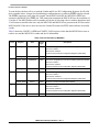
Table 1 shows the switch settings required to connect the MSC8144 and the MPC8560 to the debugger
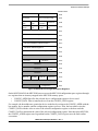
tools. Refer to the MSC8144 ADS User’s Manual for details about the switch settings.
Table 1. MSC8144ADS Switch Settings
Switch
Settings 1:8
Description
SW1
00000110
Default setting.
SW2
01101111
Host MPC8560 operates normally; disable JTAG chain for MSC8144 and MPC8560.
SW3
10010111
Default setting.
SW4
01100010
Default setting.
Note: 0 = ON, 1 = OFF
3.3
Board Control and Status Register Setting
The board control and status registers (BCSRx) are a group of 8-bit read/write registers that control or
monitor most ADS hardware options. These registers can be accessed from the host local bus. To enable
the PCI interface on the MSC8144ADS, bits 2 and 3 of BCSR1 must by set as shown in Example 1. For
details on the BCSRx bit definitions, refer to the MSC8144ADS User’s Manual.
Example 1. Enable PCI in BCSR1
void setBCSR1()
{
uint8_t *bcsr1 = (uint8_t*)0xF8000001;
*bcsr1 |= 0x30;
}
4
PCI Device Detection Example
Before the PCI host can configure each device on the bus, it must first scan the bus to determine what PCI
devices or PCI-PCI bridges are on the bus. By scanning the bus, the host can determine each device part
number, manufacturer, and device number on the bus. The PCI specification requires each PCI device to
provide 256 bytes of configuration registers. The configuration registers supply the information needed for
device configuration, including the vendor ID, device ID, command and status, revision ID, class code and
header type fields, as shown in Figure 4.
MSC8144 PCI Example Software, Rev. 0
4
Freescale Semiconductor
PCI Device Detection Example
Address Offset
Device ID
Vendor ID
0x00
PCI Status
PCI Command Config
0x04
Base Class
Code
Subclass
Code
Std Prog
Interface
Revision ID
0x08
BIST
Control
Header
Type
Latency
Timer
Cache Line
Size
0x0C
PIMMR Base Address Register
0x10
GPL Base Address Register 0
0x14
GPL Base Address Register 1
0x18
GPL Extended Base Address Register 1
0x1C
GPL Base Address Register 2
0x20
GPL Extended Base Address Register 2
0x24
Reserved
0x28
Subsystem
Device ID
Subsystem
Vendor ID
Reserved
0x30
Capabilities
Pointer
Reserved
Reserved
PCI Bus
MAX LAT
PCI Bus
MIN GNT
0x34
0x38
PCI Bus
Interr Pin
PCI Bus
Interr Line
Reserved
Reserved
0x2C
0x3C
0x40
PCI Function
Configuration
0x44
Figure 4. MSC8144 PCI Configuration Space Registers
On the MSC8144ADS, the MPC8560 host can access the MSC8144 configuration space registers through
two registers that are memory-mapped in the MPC8560 memory space:
• CONFIG_ADDR Specifies the selected device configuration register to be accessed.
• CONFIG_DATA. Data is transferred to or from the CONFIG_DATA register.
For example, the host addresses a particular device on the bus by writing to the CONFIG_ADDR with the
bus number, device number, and the configuration register to access. Next, the host either writes the
CONFIG_DATA with the value to write to the selected configuration register or the host reads the
CONFIG_DATA to determine the value of the selected configuration register. Note that in the MPC8560,
the CONFIG_ADDR register uses big-endian but the CONFIG_DATA register uses the little-endian
convention.
MSC8144 PCI Example Software, Rev. 0
Freescale Semiconductor
5
PCI Device Detection Example
To scan the bus, the host will try to read the Vendor and Device ID Configuration Registers for all valid
device number values. A target is selected during a configuration access when its IDSEL signal is selected.
The IDSEL signal acts as the chip select signal. On the MSC8144ADS, the MPC8560’s AD21 pin
connects to the MSC8144’s IDSEL pin. This connection means that the MSC8144 has a device number of
21 on bus 0. The MPC8560 has a device number of 0 on bus 0. Selecting a device number other than 0 and
21 will return an invalid value since only the MPC8560 and MSC8144 are present on the PCI bus on the
MSC8144ADS. If the device does not exist, the Vendor ID returns a 0xFFFF which indicates an invalid
vendor.
Table 2 shows the CONFIG_ADDR and CONFIG_DATA register values that the MPC8560 accesses to
read its own and the MSC8144’s vendor and device information.
Table 2. Device Detection by MPC8560
Access
Register
Value
Access
Type
1
CONFIG_ADDR
0x80000000
Write
Allow a PCI configuration access when CONFIG_DATA is accessed
Select bus number 0
Select device number 0
Access the PCI Vendor ID Configuration Register (offset 0x00)
CONFIG_DATA
0x1057
Read
Vendor ID = 0x1057 Freescale Semiconductor
CONFIG_ADDR
0x80000002
Write
Allow a PCI configuration access when CONFIG_DATA is accessed
Select bus number 0
Select device number 0
Access the PCI Device ID Configuration Register (offset 0x02)
CONFIG_DATA
0x0009
Read
Device ID = 0x0009 MPC8560
CONFIG_ADDR
0x8000A800
Write
Allow a PCI configuration access when CONFIG_DATA is accessed
Select bus number 0
Select device number 21
Access the PCI Vendor ID Configuration Register (offset 0x00)
CONFIG_DATA
0x1957
Read
Vendor ID = 0x1957 Freescale Semiconductor
CONFIG_ADDR
0x8000A802
Write
Allow a PCI configuration access when CONFIG_DATA is accessed
Select bus number 0
Select device number 21
Access the PCI Device ID Configuration Register (offset 0x02)
CONFIG_DATA
0x1400
Read
Device ID = 0x1400 MSC8144
2
3
4
Description
MSC8144 PCI Example Software, Rev. 0
6
Freescale Semiconductor
Memory Allocation Example
Example 2 shows code that runs on the MPC8560 to scan the PCI bus for devices. This code has been
simplified to scan only bus number 0.
Example 2. Scan PCI Devices
void scanDevices()
{
uint32_t i;
uint16_t VendorID, DeviceID;
uint32_t BusNum = 0;
for(i = 0; i < 0x20; i++)
{
VendorID = getPCIConfigReg16(BusNum, i, REG_VENDORID);
DeviceID = getPCIConfigReg16(BusNum, i, REG_DEVID);
if(VendorID != 0xFFFF)
{
printf(" Device found: Device %x, Bus %x, DevID = %x,
VendorID = %x\n", i, BusNum, DeviceID, VendorID);
}
}
}
5
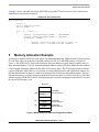
Memory Allocation Example
A transaction with the MSC8144 as the target is an inbound transaction. When the MSC8144 boots from
PCI, the boot code sets up the three inbound windows for M2, M3, and DDR memory as shown in
Figure 5. The MSC8144 PCI boot code configures the base addresses in local memory and the sizes of
these inbound windows. The PCI inbound translation address register (PITARn) defines the base address
of the inbound translation windows in the MSC8144 memory space. The PCI inbound window attribute
register (PIWARn) defines the size of a window as well as other properties and enables that window. It is
the host that allocates memory to each device on the PCI bus in a device-independent manner. The host
allocates memory by creating a memory map in the PCI memory space. It writes to each device GPL base
address register (GPLBARx) in the PCI configuration space to create a mapping between the PCI view and
the device local memory view.
MSC8144
Size depends
DDR on RCW
0x40000000
Inbound Window 2
M2
512 KB
0xC0000000
Inbound Window 0
M3
16 MB
0xD0000000
Inbound WIndow 1
Figure 5. MSC8144 Inbound Window Configuration at Boot
MSC8144 PCI Example Software, Rev. 0
Freescale Semiconductor
7
Memory Allocation Example
To determine the size requirements of the MSC8144 inbound windows, the MPC8560 writes to the
MSC8144 GPLBARx in the PCI configuration space as shown in Figure 4. These base address registers
specify the mapping of the device inbound windows in the PCI space. The host first reads these base
address registers to get the initial setting. It then writes all 1’s to these base address registers and reads them
back to determine the memory size required by the inbound window. Then the host can allocate memory
for each device in the PCI space.
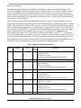
Table 3 shows the steps by which the MPC8560 determines the MSC8144 inbound window 0 memory
requirement. The MPC8560 addresses the MSC8144 GLBAR0 register by writing to the CONFIG_ADDR
register. Then it reads the CONFIG_DATA to get the value of the GPLBAR0, which defines the inbound
window 0 base address register in the PCI memory space. The host must save this value to restore later.
Next, the host writes 0xFFFFFFFF to the MSC8144 GPLBAR0 and reads back the register. The number
of bits set determines how much address space is required. For example, a GPLBAR0 value of
0xFFF80000 has the upper 13 bits of the address register set, indicating a size of 2(32-13) = 512 Kbytes.
Now, the host knows that it must allocate 512 Kbytes of memory in the PCI memory space before it can
access the MSC8144 inbound window 0. The host must then assign an address in the PCI space because
the GPLBAR0 now contains the sizing information. These steps should be repeated for GPLBAR1 and
GPLBAR2 registers to determine the memory requirements for inbound windows 1 and 2.
Table 3. Memory Allocation by MPC8560
Access
Register
Value
Access
Type
1
CONFIG_ADDR
0x8000A814
Write
Allow a PCI configuration access when CONFIG_DATA is accessed
Select bus number 0
Select device number 21
Access the GPL Base Address Register 0 (offset 0x14)
CONFIG_DATA
0x00000000
Read
GPLBAR0 = 0x00000000 inbound window 0 in PCI space
CONFIG_ADDR
0x8000A814
Write
Allow a PCI configuration access when CONFIG_DATA is accessed
Select bus number 0
Select device number 21
Access the GPL Base Address Register 0 (offset 0x14)
CONFIG_DATA
0xFFFFFFFF
Write
GPLBAR0 = 0xFFFFFFFF
CONFIG_ADDR
0x8000A814
Write
Allow a PCI configuration access when CONFIG_DATA is accessed
Select bus number 0
Select device number 21
Access the GPL Base Address Register 0 (offset 0x14)
CONFIG_DATA
0xFFF80000
Read
GPLBAR0 = 0xFFF80000 Upper 13 bits are set
Size = 2(32 - 13) = 512 KB
CONFIG_ADDR
0x8000A814
Write
Allow a PCI configuration access when CONFIG_DATA is accessed
Select bus number 0
Select device number 21
Access the GPL Base Address Register 0 (offset 0x14)
CONFIG_DATA
0xC0000000
Write
Reassign new GPLBAR0 = 0xC0000000
2
3
4
Description
MSC8144 PCI Example Software, Rev. 0
8
Freescale Semiconductor
MSC8144 Inbound Configuration Example
In this example, the host assigns a chunk of memory in the PCI memory space to map the MSC8144
inbound window in M2. The host configures the MSC8144 GPLBAR0 = 0xC0000000 to give a one-to-one
mapping between the PCI view and the MSC8144 local view, as shown in Figure 6.
MPC8560
PCI View
512 KB
MSC8144
GPLBAR0 =
0xC0000000
512 KB
0xC0000000
Figure 6. Example MSC8144 GPLBAR0 Configuration
Example 3 shows the function called by the MPC8560 to calculate the size of a device inbound window.
Example 3. Determine Memory Requirement
uint32_t getWindowSize(uint32_t BusNum, uint32_t DevNum, uint32_t Reg)
{
uint32_t new, orig;
uint32_t size;
// Read CfgReg
orig = getPCIConfigReg32(BusNum, DevNum, Reg);
// Write all 1’s
setPCIConfigReg32(BusNum, DevNum, Reg, 0xFFFFFFFF);
// Read back to determine size
new = getPCIConfigReg32(BusNum, DevNum, Reg);
// Restore orig register value
setPCIConfigReg32(BusNum, DevNum, Reg, orig);
// Calculate size required by agent
if (new & 1)
size = (~new | 3) + 1;
// I/O space
else
size = (~new | 0xF) + 1;
// Memory space
return size;
}
6
MSC8144 Inbound Configuration Example
An inbound transaction in which the MSC8144 is the target means that the host MPC8560 is the bus master
or the initiator performing an outbound transaction. Outbound transactions require address translation to
map transactions from the internal address space of the MPC8560 to the external PCI address space.
MSC8144 PCI Example Software, Rev. 0
Freescale Semiconductor
9
MSC8144 Inbound Configuration Example
MPC8560 registers to handle the address translation task are as follows:
• PCI outbound translation address register (POTARn) selects the base address of the external PCI
address space for hits in the outbound window.
• PCI outbound window base address register (POWBARn) points to the base address of the
outbound window in the MPC8560 local address space.
• PCI outbound window attributes register (POWARn) enables the address translation window,
specifies the transaction type, and defines the window size.
Table 4 shows the outbound window 1 of size 512 Kbytes starting at 0x80000000 in the MPC8560 local
address space for translation to the external PCI address starting at 0xC0000000.
Table 4. MPC8560 PCI Outbound Register Settings
Register
Value
Description
POTAR1
0x000C0000
Set base address 0xC0000000 as the translated address in the PCI address space
POWBAR1
0x00080000
Set base address 0x80000000 as the outbound address from the MPC8560
POWAR1
0x80044012
Enable the outbound translation window 1
Enable memory read and write transactions
Set translation window 1 size as 512 Kbytes
Figure 7 depicts the MPC8560 outbound address translation mapping. An access to the MPC8560 local
address starting at 0x80000000 is routed to the PCI memory space starting at 0xC0000000. Notice that the
PCI address is configured to be the same as the local address for a simple one-to-one mapping. The left
side of the dotted line gives register settings on the MPC8560 side, and the right side of the dotted line
gives register settings on the MSC8144 side. Note that the MPC8560 POTAR must have the same value
as the MSC8144 GPLBAR.
MPC8560
MSC8144
PCI View
POBAR =
0x80000000
POTAR =
0xC0000000
Host MPC8560 Side
GPLBAR =
0xC0000000
PITAR =
0xC0000000
Agent MSC8144 Side
Figure 7. MPC8560 Outbound / MSC8144 Inbound Address Mapping
MSC8144 PCI Example Software, Rev. 0
10
Freescale Semiconductor
MSC8144 CCSR Mapping Example
Before the MSC8144 DSP can respond to memory accesses, the MPC8560 processor must configure the
MSC8144 PCI command configuration register, which has an offset of 0x04 in the PCI configuration
space. The MEM bit must be set to allow the MSC8144 to respond to memory accesses. Figure 8 shows
an example in which the MSC8144 performs an inbound transaction. The left screenshot shows the
MPC8560 writing the value 0x11223344 to its local outbound window. This address is translated to the
PCI address that is mapped to the MSC8144 local inbound window. The right screenshot shows the
MSC8144 reading the same value from its local inbound window.
1. MPC8560 writes data to outbound window
2. MSC8144 reads data from inbound window
Figure 8. MSC8144 Inbound Example
7
MSC8144 CCSR Mapping Example
Before we look at an example MSC8144 outbound transaction, let us first consider how to configure the
host MPC8560 to view the MSC8144 configuration control and status registers (CCSR) map. The CCSR
address space includes control and status registers for DMA, CLASS, DDR, clock, I2C, timers, TDM,
GPIO, PCI, RapidIO, and so on.
External masters do not need the location of a device’s CCSR memory space. Instead, they access a
device’s CCSR through a window defined by the PIMMR base address configuration register in the
configuration register space, as shown in Figure 4. The PIMMR defines the address for accessing the local
CCSR memory space of a device. It specifies an address in the PCI space where the CCSR space is
mapped.
The CCSR memory space is 32 Mbytes. Subtracting 32 Mbytes from the top of the MSC8144 address
space gives the CCSR base address of 0xFE000000. In this example, the host configures PIMMR to
0x30000000 through the CONFIG_ADDR and CONFIG_DATA configuration access registers. The host
also configures another outbound window at 0x90000000 so that transactions from this space are mapped
to the PCI space at 0x30000000. Figure 9 shows a diagram of the CCSR address space mapping, and
Table 5 shows how the MPC8560 configures the MSC8144 PIMMR base address.
MSC8144 PCI Example Software, Rev. 0
Freescale Semiconductor
11
MSC8144 CCSR Mapping Example
MPC8560
MSC8144
PCI View
POTAR =
0x30000000
PIMMR =
0x30000000
POBAR =
0x90000000
0xFE000000
CCSR
Host MPC8560 Side
Agent MSC8144 Side
Figure 9. MSC8144 CCSR Address Space Mapping
Table 5. MPC8560 Outbound Window for MSC8144 CCSR Mapping
Register
Value
Access
Type
CONFIG_ADDR
0x8000A810
Write
Allow a PCI configuration access when CONFIG_DATA is accessed
Select bus number 0
Select device number 21
Access the PIMMR Base Address Register (offset 0x10)
CONFIG_DATA
0x30000000
Write
PIMMR = 0x30000000 CCSR mapping in PCI space
Description
For example, if the MPC8560 needs to read the MSC8144 PCI error status register (PCI_ESR), then the
MPC8560 accesses the outbound window that maps to the MSC8144 CCSR space. The PCI_ESR is at
0xFFF7A000 in the MSC8144 local space. With a CCSR base address of 0xFE000000, the PCI_ESR has
an offset of 0x01F7A000 from the CCSR base. To access this register, the MPC8560 needs to read the
following address:
Eqn. 1
PCI_ESR = 0x90000000 + (0xFFF7A000 - 0xFE000000) = 0x91F7A000
As you can see, the PIMMR allows an external master to access a device’s internal memory-mapped
registers without knowing where the CCSR resides. This is especially useful because the CCSR base
address is programmable so that the PCI host can read and write the MSC8144 memory-mapped registers.
MSC8144 PCI Example Software, Rev. 0
12
Freescale Semiconductor
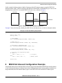
MSC8144 Outbound Configuration Example
8
MSC8144 Outbound Configuration Example
In Section 5, “Memory Allocation Example,” we noted that the MSC8144 configures three inbound
windows for M2, M3, and DDR at bootup. The boot code does not configure the outbound windows, so
the host must configure them. Knowing how the MPC8560 can access the MSC8144 memory-mapped
registers, we allow the MPC8560 to set up the MSC8144 outbound window using the PIMMR. The
MSC8144 defines an outbound memory window in the address range 0xE0000000–0xE7FFFFFF. Both
the configuration access registers CONFIG_ADDR and CONFIG_DATA fall within this 128 Mbyte
window. If the address is not 0xE7FFFFF0 (CONFIG_ADDR) or 0xE7FFFFF4 (CONFIG_DATA), then
the transaction is forwarded to the PCI port.
When the MSC8144 initiates a transaction, the PCI outbound base address register (POBARn) defines the
location of the outbound translation in MSC8144 memory space. The POTARn defines the starting-point
of the outbound translation address in the destination PCI memory space. The POCMRn defines the size
of an outbound translation window, defines properties, and enables that window.
Mapping the MSC8144 outbound window to the PCI space with a one-to-one mapping means that both
the POBAR0 and POTAR0 registers are set to map a window at 0xE0000000. The MPC8560 writes to
these registers through the PIMMR mapping in the PCI space. The MSC8144 can access the POTAR0
locally at 0xFFF7A100. Based on the settings for mapping the CCSR map, the MPC8560 can access the
MSC8144 POTAR0 from its local space at 0x91F7A100. Similarly, it can access the MSC8144 POBAR0
and POCMR0 registers from 0x91F7A108 and 0x91F7A110, respectively.
Eqn. 2
POTAR0 = 0x90000000 + (0xFFF7A100 - 0xFE000000) = 0x91F7A100
Eqn. 3
POBAR0 = 0x90000000 + (0xFFF7A108 - 0xFE000000) = 0x91F7A108
Eqn. 4
POCMR0 = 0x90000000 + (0xFFF7A110 - 0xFE000000) = 0x91F7A110
Suppose the MPC8560 receives inbound transactions at address 0x00000000 so that the mapping is as
shown in Figure 10. The MPC8560 configures the MSC8144 outbound window register settings as shown
in Table 6. Its inbound window register settings are shown in Table 7.
MSC8144 PCI Example Software, Rev. 0
Freescale Semiconductor
13
MSC8144 Outbound Configuration Example
MPC8560
MSC8144
PCI View
PITAR =
0x00000000
PIBAR =
0xE0000000
POTAR =
0xE0000000
Host MPC8560 Side
POBAR =
0xE0000000
Agent MSC8144 Side
Figure 10. MSC8144 Outbound / MPC8560 Inbound Address Mapping
Table 6. MSC8144 PCI Outbound Registers Settings
MSC8144
Register
Address as Visible
to MSC8144
Address as Visible
to MPC8560
POTAR0
0xFFF7A100
0x91F7A100
0x000E0000 Set base address 0xE0000000 as the translated
address in the PCI memory space
POBAR0
0xFFF7A108
0x91F7A108
0x000E0000 Set base address 0xE0000000 as the outbound
window 0 in the MSC8144 local memory space
POCMR0
0xFFF7A110
0x91F7A110
0xA00F8000 Enable the inbound translation window 0
Map window 0 to PCI memory space
Enable streaming
Set translation window 0 size as 128 MB
Value
Description
Table 7. MPC8560 PCI Inbound Registers Settings
Register
Value
Description
PITAR1
0x00000000
Set base address 0x00000000 as the translated address in the local MPC8560
memory space
PIWBAR1
0x000E0000
Set base address 0xE0000000 as the address in the PCI memory space
PIWAR1
0xA0F5501B
Enable the inbound translation window 1
Inbound window 1 is prefetchable
Target interface is local memory
Enable read and write with snooping
Set translation window 1 size as 256 MB
MSC8144 PCI Example Software, Rev. 0
14
Freescale Semiconductor
Cache Line Size
Before the MSC8144 can initiate PCI accesses, the MPC8560 must configure the MSC8144 PCI bus
command register, which has an offset of 0x04 in the PCI configuration space as shown in Figure 4. The
BMST bit must be set so that the MSC8144 behaves as a bus master.
In Figure 11, the MSC8144 performs an outbound transaction. The bottom screenshot shows the
MSC8144 writing the value 0xDEADBEEF to its local outbound window. This address is translated to the
PCI address that is mapped to the MPC8560 local inbound window. The top screenshot shows the
MPC8560 reading the same value from its local inbound window.
2. MPC8560 reads data from inbound window
1. MSC8144 writes data to outbound window
Figure 11. MSC8144 Outbound Example
9
Cache Line Size
The MSC8144 PCI controller has an internal cache line of 32 bytes. Although the cache line size register
in the configuration space is writable, only the value 8 is valid. This value indicates a cache line of 8
doublewords or 32 bytes. When the MSC8144 acts as a target, the bus command PCI MEMORY READ fetches
a cache line of data. 32 bytes of data are fetched, regardless of the size requested by the initiator. In the
MSC8144, there is no difference between the PCI MEMORY READ and PCI MEMORY READ LINE commands
because the entire cache line is fetched in both cases. The PCI MEMORY READ MULTIPLE command is also
similar, but it supports prefetching. This command causes a prefetch of the next cache line.
10 Latency Timer
The minimum grant (MIN_GNT) space register defines the minimum time, in increments of 250 ns, during
which the master retains ownership of the bus for adequate performance. This read-only register is useful
in determining the value to be programmed into the bus master latency timer (LT) configuration register.
Because the MSC8144 PCI controller is a bridge between PCI and local memory, it does not have specific
requirements for the LT when it operates as a bus master. Therefore, MIN_GNT is hard-wired to zero.
MSC8144 PCI Example Software, Rev. 0
Freescale Semiconductor
15
Interrupt Handling
Configuration software should configure LT according to system requirements. The LT value is
system-dependent and this value should be tuned to maximize utilization without starving the other PCI
bus masters. For example, leaving the LT at zero may require the master to rearbitrate for the bus for long
data transfers, but setting it to the maximum value may potentially keep other masters from accessing the
bus.
11 Interrupt Handling
In many PCI devices, the INTA, INTB, INTC, and INTD pins signal interrupts to the PCI bus. The
interrupt pin configuration register in the configuration space at offset 0x3D indicates which of these four
pins the device uses. However, the MSC8144 does not implement these four PCI interrupt pins. It is
recommended that the general-purpose interrupt request lines IRQ0:15 and INT_OUT be used to route
interrupt sources.
12 MPC8560 Host Configuration Code
/////////////////////////////////////////////////////////////////////////
// Switch settings:
// SW1 00000110 PCI boot
// SW2 01101111 Disable JTAG chain
// SW3 10010111 PCI (256M DDR)
// SW4 01100010
/////////////////////////////////////////////////////////////////////////
#include <stdio.h>
#include "mpc8560pci.h"
// Check which ADx pin is connected to IDSEL
#define MSC8144_PCIDEVICENUM21
#define MPC8560_PCIDEVICENUM0
// PCI device id for MSC8144
#define MSC8144_PCIDEVID0x1400
#define MPC8560_PCIDEVID0x0009
#define MPC8560_PCIVENDORID0x1057
#define MSC8144_PCIVENDORID0x1957
#define
#define
#define
#define
#define
#define
#define
#define
#define
uint32_t
uint32_t
uint32_t
uint32_t
uint32_t
READ_UINT8(data, arg)
READ_UINT16(data, arg)
READ_UINT32(data, arg)
GET_UINT8(arg)
GET_UINT16(arg)
GET_UINT32(arg)
WRITE_UINT8(arg, data)
WRITE_UINT16(arg, data)
WRITE_UINT32(arg, data)
IMMR8144Local
OutboundLocal
InboundLocal
IMMR8144PCI
OutboundPCI
=
=
=
=
=
data = (uint8_t)(arg)
data = (uint16_t)(arg)
data = (uint32_t)(arg)
(uint8_t)(arg)
(uint16_t)(arg)
(uint32_t)(arg)
arg = (uint8_t)(data)
arg = (uint16_t)(data)
arg = (uint32_t)(data)
0x90000000;
0x80000000;
0x00000000;
0x30000000;
0xC0000000;
MSC8144 PCI Example Software, Rev. 0
16
Freescale Semiconductor
MPC8560 Host Configuration Code
uint32_t InboundPCI
uint32_t PCI8144BASE
= 0xE0000000;
= 0x01F7A000;
msc8144_pci_regs *msc8144;
mpc8560_pci_regs *mpc8560 = (mpc8560_pci_regs*)0x40008000;
void setBCSR1();
uint32_t SwapLong(uint32_t);
uint32_t ConstructConfigWord (uint32_t ,uint32_t, uint32_t);
void setPIMMR(uint32_t);
void scanDevices();
uint32_t getWindowSize(uint32_t, uint32_t, uint32_t);
void setOutbound1(uint32_t, uint32_t, uint32_t);
void setOutbound2(uint32_t, uint32_t, uint32_t);
uint32_t calcWindowSize(uint32_t);
void writePCIConfigReg(uint32_t, uint32_t, uint32_t, uint32_t);
void setPCIConfigReg32(uint32_t, uint32_t, uint32_t, uint32_t);
void setPCIConfigReg16(uint32_t, uint32_t, uint32_t, uint16_t);
void setPCIConfigReg8(uint32_t, uint32_t, uint32_t, uint8_t);
uint32_t readPCIConfigReg(uint32_t, uint32_t, uint32_t);
uint32_t getPCIConfigReg32(uint32_t, uint32_t, uint32_t);
uint16_t getPCIConfigReg16(uint32_t, uint32_t, uint32_t);
uint8_t getPCIConfigReg8(uint32_t, uint32_t, uint32_t);
uint32_t SwapLong(uint32_t value)
{
value = ((value & 0xFF)
((value & 0xFF00)
((value & 0xFF0000UL)
((value & 0xFF000000UL)
return value;
}
<< 24) |
<< 8) |
>> 8) |
>> 24) ;
uint32_t ConstructConfigWord (uint32_t BusNum,uint32_t DevNum,uint32_t RegNum)
{
uint32_t value;
uint32_t FuncNum=0x0;
value = (
((BusNum
((DevNum
((FuncNum
((RegNum
ENABLE
&
&
&
&
0xFF)
0xFF)
0xFF)
0xFC)
<< 16) |
<< 11) |
<< 8) |
) |
) ;
return value;
}
void writePCIConfigReg(uint32_t BusNum, uint32_t DevNum, uint32_t Reg, uint32_t Data)
{
uint32_t cfg_addr;
uint32_t data32;
data32 = SwapLong(Data);
if ((Reg & 0x3) == 1)
data32 = data32 >> 8;
MSC8144 PCI Example Software, Rev. 0
Freescale Semiconductor
17
MPC8560 Host Configuration Code
else if ((Reg &
data32
else if ((Reg &
data32
0x3) == 2)
= data32 >> 16;
0x3) == 3)
= data32 >> 24;
cfg_addr = ConstructConfigWord(BusNum, DevNum, Reg);
WRITE_UINT32(mpc8560->config_addr, cfg_addr);
WRITE_UINT32(mpc8560->config_data, data32);
}
void setPCIConfigReg32(uint32_t BusNum, uint32_t DevNum, uint32_t Reg, uint32_t Data)
{
writePCIConfigReg(BusNum, DevNum, Reg, Data);
}
void setPCIConfigReg16(uint32_t BusNum, uint32_t DevNum, uint32_t Reg, uint16_t Data)
{
writePCIConfigReg(BusNum, DevNum, Reg, Data);
}
void setPCIConfigReg8(uint32_t BusNum, uint32_t DevNum, uint32_t Reg, uint8_t Data)
{
writePCIConfigReg(BusNum, DevNum, Reg, Data);
}
uint32_t readPCIConfigReg(uint32_t BusNum, uint32_t DevNum, uint32_t Reg)
{
uint32_t cfg_addr;
uint32_t cfg_data;
cfg_addr = ConstructConfigWord(BusNum, DevNum, Reg);
WRITE_UINT32(mpc8560->config_addr, cfg_addr);
READ_UINT32(cfg_data, mpc8560->config_data);
cfg_data = SwapLong(cfg_data);
if ((Reg & 0x3) == 1)
cfg_data = cfg_data >> 8;
else if ((Reg & 0x3) == 2)
cfg_data = cfg_data >> 16;
else if ((Reg & 0x3) == 3)
cfg_data = cfg_data >> 24;
return cfg_data;
}
uint32_t getPCIConfigReg32(uint32_t BusNum, uint32_t DevNum, uint32_t Reg)
{
return (uint32_t)readPCIConfigReg(BusNum, DevNum, Reg);
}
uint16_t getPCIConfigReg16(uint32_t BusNum, uint32_t DevNum, uint32_t Reg)
{
return (uint16_t)readPCIConfigReg(BusNum, DevNum, Reg);
}
MSC8144 PCI Example Software, Rev. 0
18
Freescale Semiconductor
MPC8560 Host Configuration Code
uint8_t getPCIConfigReg8(uint32_t BusNum, uint32_t DevNum, uint32_t Reg)
{
return (uint8_t)readPCIConfigReg(BusNum, DevNum, Reg);
}
void scanDevices()
{
uint32_t i;
uint16_t VendorID, DeviceID;
uint32_t BusNum = 0;
for(i = 0; i < 0x100; i++)
{
VendorID = getPCIConfigReg16(BusNum, i, REG_VENDORID);
DeviceID = getPCIConfigReg16(BusNum, i, REG_DEVID);
if(VendorID != 0xFFFF)
{
printf(" Device found: Device %x, Bus %x, DevID = %x, VendorID =
%x\n",
i, BusNum, DeviceID, VendorID);
}
}
}
void setBCSR1()
{
uint8_t *bcsr1 = (uint8_t*)0xF8000001;
*bcsr1 |= 0x30;
}
uint32_t getWindowSize(uint32_t BusNum, uint32_t DevNum, uint32_t Reg)
{
uint32_t new, orig;
uint32_t size;
// Read CfgReg
orig = getPCIConfigReg32(BusNum, DevNum, Reg);
// Write all 1’s
setPCIConfigReg32(BusNum, DevNum, Reg, 0xFFFFFFFF);
// Read back to determine size
new = getPCIConfigReg32(BusNum, DevNum, Reg);
// Restore orig register value
setPCIConfigReg32(BusNum, DevNum, Reg, orig);
// Calculate size required by agent
if (new & 1)
size = (~new | 3) + 1;// I/O space
else
size = (~new | 0xF) + 1;// Memory space
return size;
}
MSC8144 PCI Example Software, Rev. 0
Freescale Semiconductor
19
MPC8560 Host Configuration Code
void setOutbound2(uint32_t LocalAddr, uint32_t PCIAddr, uint32_t WindowSize)
{
// PCI address
mpc8560->potar2
= PCIAddr
>> 12;
// Local Addr
mpc8560->powbar2
= LocalAddr >> 12;
// Enable, memory read/write, window size
mpc8560->powar2
= 0x80044000 | WindowSize ;
}
void setOutbound1(uint32_t LocalAddr, uint32_t PCIAddr, uint32_t WindowSize)
{
// PCI address
mpc8560->potar1
= PCIAddr
>> 12;
// Local Addr
mpc8560->powbar1
= LocalAddr >> 12;
// Enable, memory read/write, window size
mpc8560->powar1
= 0x80044000 | WindowSize ;
}
uint32_t calcWindowSize(uint32_t Size)
{
int i;
uint32_t WindowSize = 0;
for(i = 0; i < 32; i++)
{
if(Size & 0x01)
{
WindowSize += i;
}
Size = Size >> 1;
}
WindowSize = WindowSize - 1;
return WindowSize;
}
void main()
{
uint32_t
uint32_t
uint32_t
uint32_t
uint16_t
uint32_t
BusNum = 0;
*outbound, *inbound;
size;
windowstart;
status_8144;
data;
// Set BCSR1[RGMII1EN and RGMII2EN] = 1 (Disable) to select PCI/UTP instead of RGMII
setBCSR1();
// Scan devices on the bus
MSC8144 PCI Example Software, Rev. 0
20
Freescale Semiconductor
MPC8560 Host Configuration Code
scanDevices();
// Set 8560 as the arbiter
setPCIConfigReg16(BusNum, MPC8560_PCIDEVICENUM, REG_ARBITER, 0);
// Set latency timer to max clock cycles to generate stop
setPCIConfigReg8(BusNum, MPC8560_PCIDEVICENUM, REG_BUSLATENCY, 0xF8);
//
//
//
//
//
************************************************************
8560 Outbound / 8144 Inbound
8560 0x8000_0000 --> PCI 0x8000_0000 --> 8144 0xC000_0000
Size 512KB
************************************************************
// Determine window sizes for 8144 GPLx = 0x0010_0000
size = getWindowSize(BusNum, MSC8144_PCIDEVICENUM, REG_GPLBAR0); //M2
// Reassign 8144 inbound window 0 start addr in PCI memory space
setPCIConfigReg32(BusNum, MSC8144_PCIDEVICENUM, REG_GPLBAR0, OutboundPCI);
// Read 8144 PCI base inbound window = 0x2000_0008 (prefetchable)
windowstart = getPCIConfigReg32(BusNum, MSC8144_PCIDEVICENUM, REG_GPLBAR0);
// Set outbound window local address 0x80000000, PCI address 0x20000000, 512KB size
setOutbound1(OutboundLocal, OutboundPCI, calcWindowSize(size));
//
//
//
//
//
//
************************************************************
8144 Outbound / 8560 Inbound
8144 0xE000_0000 --> PCI 0xE000_0000 --> 8560 0x0000_0000
Size 256MB
************************************************************
Set inbound window local address 0x00000000, PCI address 0xE0000000
// PCI address
mpc8560->piwbar1 = InboundPCI
// Local Addr
mpc8560->pitar1
>> 12;
= InboundLocal >> 12;
// Enable, prefetch, target i/f local mem, r/w snoop, 256MB size
mpc8560->piwar1 = 0xA0F5501B;
//
//
//
//
//
************************************************************
8144 PIMMR memory mapped space
8560 0x9000_0000 --> PCI 0x3000_0000 --> 8144 0xFE00_0000 (IMMR)
Size 32MB
************************************************************
// Determine window size and set start addr for 8144 PIMMR
size = getWindowSize(BusNum, MSC8144_PCIDEVICENUM, REG_PIMMRBACR);//IMMR 32MB
// Reassign 8144 inbound window 1 start addr in PCI memory space
setPCIConfigReg32(BusNum, MSC8144_PCIDEVICENUM, REG_PIMMRBACR, IMMR8144PCI);
windowstart = getPCIConfigReg32(BusNum, MSC8144_PCIDEVICENUM, REG_PIMMRBACR);
// Set outbound window local address 0x00000000, PCI address 0x30000000, 32MB size
setOutbound2 (IMMR8144Local, IMMR8144PCI, calcWindowSize(size));
MSC8144 PCI Example Software, Rev. 0
Freescale Semiconductor
21
MPC8560 Header File
// BMST=1, MEM=1, PERR/SERR=1
setPCIConfigReg16(BusNum, MPC8560_PCIDEVICENUM, REG_BUSCMD, 0x0146);
// BMST=1, MEM=1, PERR/SERR=1
setPCIConfigReg16(BusNum, MSC8144_PCIDEVICENUM, REG_BUSCMD, 0x0146);
//
//
//
//
************************************************************
Now 8560 can access 8144 memory-mapped registers to set up
8144’s outbound windows
************************************************************
PCI8144BASE = PCI8144BASE + IMMR8144Local;
msc8144 = (msc8144_pci_regs*)PCI8144BASE;
// MSC8144 outbound 0 enable, prefetch, streaming
msc8144->outbound[0].potar = InboundPCI >> 12;
msc8144->outbound[0].pobar = 0x000E0000;
msc8144->outbound[0].pocmr = 0xA00F8000;
//
//
//
//
//
//
************************************************************
Perform outbound transaction
8560 writes to 8144 memory
Step through code here to write to memory
Then in 8144 project, step through code to read memory
************************************************************
outbound = (uint32_t *)OutboundLocal;
*outbound = (uint32_t)0x11223344;
//
//
//
//
//
//
************************************************************
Perform inbound transaction
8144 writes to 8560 memory
In 8144 project, step through code to write to memory
Then step through code here to read memory
************************************************************
inbound = (uint32_t *)InboundLocal;
data = *inbound;
}
13 MPC8560 Header File
#include "os_datatypes.h"
// CONFIG_ADDR bits
#define ENABLE
0x80000000
// Configuration Access Registers
#define REG_VENDORID
#define REG_DEVID
#define REG_BUSCMD
#define REG_BUSSTATUS
0x0000
0x0002
0x0004
0x0006
MSC8144 PCI Example Software, Rev. 0
22
Freescale Semiconductor
MPC8560 Header File
#define
#define
#define
#define
#define
#define
#define
#define
#define
#define
#define
#define
#define
#define
#define
#define
#define
#define
#define
#define
#define
#define
#define
REG_REVID
REG_BUSPROGIF
REG_SUBCLASS
REG_BASECLASS
REG_CACHELINESZ
REG_BUSLATENCY
REG_HDRTYPE
REG_BISTCTL
REG_PIMMRBACR
REG_GPLBAR0
REG_GPLBAR1
REG_GPLEXTBAR1
REG_GPLBAR2
REG_GPLEXTBAR2
REG_SUBSYSVENDORID
REG_SUBSYSID
REG_CAPABILITYPTR
REG_INTERRLINE
REG_INTERRPIN
REG_MINGNT
REG_MAXLAT
REG_FUNCTION
REG_ARBITER
#define
#define
#define
#define
#define
#define
#define
#define
#define
#define
#define
#define
#define
#define
#define
#define
#define
#define
#define
#define
#define
SIZE_4KB
SIZE_8KB
SIZE_16KB
SIZE_32KB
SIZE_64KB
SIZE_128KB
SIZE_256KB
SIZE_512KB
SIZE_1MB
SIZE_2MB
SIZE_4MB
SIZE_8MB
SIZE_16MB
SIZE_32MB
SIZE_64MB
SIZE_128MB
SIZE_256MB
SIZE_512MB
SIZE_1GB
SIZE_2GB
SIZE_4GB
typedef struct
{
volatile
volatile
volatile
volatile
0x0008
0x0009
0x000A
0x000B
0x000C
0x000D
0x000E
0x000F
0x0010
0x0014
0x0018
0x001C
0x0020
0x0024
0x002C
0x002E
0x0034
0x003C
0x003D
0x003E
0x003F
0x0044
0x0046
0x0B
0x0C
0x0D
0x0E
0x0F
0x10
0x11
0x12
0x13
0x14
0x15
0x16
0x17
0x18
0x19
0x1A
0x1B
0x1C
0x1D
0x1E
0x1F
uint32_tconfig_addr;
uint32_tconfig_data;
uint32_tint_ack;
uint8_treserved[0xBF4];
volatile uint32_tpotar0;
volatile uint32_tpotear0;
volatile uint32_tpowbar0;
MSC8144 PCI Example Software, Rev. 0
Freescale Semiconductor
23
MPC8560 Header File
volatile uint8_treserved0[0x4];
volatile uint32_tpowar0;
volatile uint8_treserved1[0xC];
volatile
volatile
volatile
volatile
volatile
volatile
uint32_tpotar1;
uint32_tpotear1;
uint32_tpowbar1;
uint8_treserved2[0x4];
uint32_tpowar1;
uint8_treserved3[0xC];
volatile
volatile
volatile
volatile
volatile
volatile
uint32_tpotar2;
uint32_tpotear2;
uint32_tpowbar2;
uint8_treserved4[0x4];
uint32_tpowar2;
uint8_treserved5[0xC];
volatile
volatile
volatile
volatile
volatile
volatile
uint32_tpotar3;
uint32_tpotear3;
uint32_tpowbar3;
uint8_treserved6[0x4];
uint32_tpowar3;
uint8_treserved7[0xC];
volatile
volatile
volatile
volatile
volatile
volatile
uint32_tpotar4;
uint32_tpotear4;
uint32_tpowbar4;
uint8_treserved8[0x4];
uint32_tpowar4;
uint8_treserved9[0x10C];
volatile
volatile
volatile
volatile
volatile
volatile
uint32_tpitar3;
uint8_treserved10[0x4];
uint32_tpiwbar3;
uint32_tpiwbear3;
uint32_tpiwar3;
uint8_treserved11[0xC];
volatile
volatile
volatile
volatile
volatile
volatile
uint32_tpitar2;
uint8_treserved12[0x4];
uint32_tpiwbar2;
uint32_tpiwbear2;
uint32_tpiwar2;
uint8_treserved13[0xC];
volatile
volatile
volatile
volatile
volatile
volatile
uint32_tpitar1;
uint8_treserved14[0x4];
uint32_tpiwbar1;
uint32_tpiwbear1;
uint32_tpiwar1;
uint8_treserved15[0xC];
} mpc8560_pci_regs;
MSC8144 PCI Example Software, Rev. 0
24
Freescale Semiconductor
MPC8560 Header File
typedef struct
{
volatile uint32_t
volatile uint8_t
volatile uint32_t
volatile uint8_t
volatile uint32_t
volatile uint8_t
} pci_outbound_window_t;
typedef struct
{
volatile uint32_t
volatile uint8_t
volatile uint32_t
volatile uint32_t
volatile uint32_t
volatile uint8_t
} pci_inbound_window_t;
potar;
reserved1[0x4];
pobar;
reserved2[0x4];
pocmr;
reserved3[0x4];
/* PCI Outbound Translation Address Register */
pitar;
reserved1[0x4];
pibar;
piebar;
piwar;
reserved2[0x4];
/* PCI Inbound Translation Address Register */
typedef struct
{
/* PCI Error Management Registers
volatile uint32_t pci_esr;
/*
volatile uint32_t pci_ecdr;
/*
volatile uint32_t pci_err;
/*
volatile uint32_t pci_eatcr;
/*
volatile uint32_t pci_eacr;
/*
volatile uint32_t pci_eeacr;
/*
volatile uint32_t pci_edcr;
/*
volatile uint8_t reserved1[0x038
/* PCI Outbound Base Address Register */
/* PCI Outbound Comparison Mask Register */
/* PCI Inbound Base Address Register */
/* PCI Inbound Extended Base Address Register */
/* PCI Inbound Window Attributes Register */
*/
PCI error
PCI error
PCI error
PCI error
PCI error
PCI error
PCI error
- 0x01C];
status register */
capture disable register */
enable register */
attributes capture register */
address capture register */
extended address capture register */
data capture register */
/* PCI Inbound Registers */
pci_inbound_window_t inbound2;
pci_inbound_window_t inbound1;
pci_inbound_window_t inbound0;
volatile uint8_t
reserved2[0x100 - 0x080];
/* PCI Outbound Registers */
pci_outbound_window_t outbound[6];
volatile uint8_t
reserved3[0x1F8 - 0x190];
/* PCI Control Registers */
volatile uint32_t dtcr;
/* Discard Timer Control Register */
volatile uint8_t reserved4[0x200 - 0x1FC];
} msc8144_pci_regs;
MSC8144 PCI Example Software, Rev. 0
Freescale Semiconductor
25
MPC8560 Header File
THIS PAGE INTENTIONALLY LEFT BLANK
MSC8144 PCI Example Software, Rev. 0
26
Freescale Semiconductor
MPC8560 Header File
THIS PAGE INTENTIONALLY LEFT BLANK
MSC8144 PCI Example Software, Rev. 0
Freescale Semiconductor
27
How to Reach Us:
Home Page:
www.freescale.com
Web Support:
http://www.freescale.com/support
USA/Europe or Locations Not Listed:
Freescale Semiconductor, Inc.
Technical Information Center, EL516
2100 East Elliot Road
Tempe, Arizona 85284
+1-800-521-6274 or
+1-480-768-2130
www.freescale.com/support
Europe, Middle East, and Africa:
Freescale Halbleiter Deutschland GmbH
Technical Information Center
Schatzbogen 7
81829 Muenchen, Germany
+44 1296 380 456 (English)
+46 8 52200080 (English)
+49 89 92103 559 (German)
+33 1 69 35 48 48 (French)
www.freescale.com/support
Information in this document is provided solely to enable system and software
implementers to use Freescale Semiconductor products. There are no express or
implied copyright licenses granted hereunder to design or fabricate any integrated
circuits or integrated circuits based on the information in this document.
Freescale Semiconductor reserves the right to make changes without further notice to
any products herein. Freescale Semiconductor makes no warranty, representation or
guarantee regarding the suitability of its products for any particular purpose, nor does
Freescale Semiconductor assume any liability arising out of the application or use of
any product or circuit, and specifically disclaims any and all liability, including without
limitation consequential or incidental damages. “Typical” parameters which may be
provided in Freescale Semiconductor data sheets and/or specifications can and do
vary in different applications and actual performance may vary over time. All operating
parameters, including “Typicals” must be validated for each customer application by
customer’s technical experts. Freescale Semiconductor does not convey any license
Japan:
Freescale Semiconductor Japan Ltd.
Headquarters
ARCO Tower 15F
1-8-1, Shimo-Meguro, Meguro-ku
Tokyo 153-0064
Japan
0120 191014 or
+81 3 5437 9125
[email protected]
under its patent rights nor the rights of others. Freescale Semiconductor products are
Asia/Pacific:
Freescale Semiconductor Hong Kong Ltd.
Technical Information Center
2 Dai King Street
Tai Po Industrial Estate
Tai Po, N.T., Hong Kong
+800 2666 8080
[email protected]
claims, costs, damages, and expenses, and reasonable attorney fees arising out of,
For Literature Requests Only:
Freescale Semiconductor
Literature Distribution Center
P.O. Box 5405
Denver, Colorado 80217
+1-800 441-2447 or
+1-303-675-2140
Fax: +1-303-675-2150
LDCForFreescaleSemiconductor
@hibbertgroup.com
Document Number: AN3098
Rev. 0
11/2006
not designed, intended, or authorized for use as components in systems intended for
surgical implant into the body, or other applications intended to support or sustain life,
or for any other application in which the failure of the Freescale Semiconductor product
could create a situation where personal injury or death may occur. Should Buyer
purchase or use Freescale Semiconductor products for any such unintended or
unauthorized application, Buyer shall indemnify and hold Freescale Semiconductor
and its officers, employees, subsidiaries, affiliates, and distributors harmless against all
directly or indirectly, any claim of personal injury or death associated with such
unintended or unauthorized use, even if such claim alleges that Freescale
Semiconductor was negligent regarding the design or manufacture of the part.
Freescale™ and the Freescale logo are trademarks of Freescale Semiconductor, Inc.
The Power Architecture and Power.org word marks and the Power and Power.org
logos and related marks are trademarks and service marks licensed by Power.org.
IEEE nnn, nnn,nnn, and nnn are registered trademarks of the Institute of Electrical and
Electronics Engineers, Inc. (IEEE). This product is not endorsed or approved by the
IEEE. All other product or service names are the property of their respective owners.
© Freescale Semiconductor, Inc., 2006. All rights reserved.