1
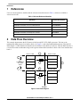
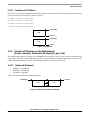
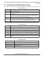
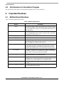
Freescale Semiconductor
AN2431
Rev. 1, 05/2005
Application Note
PowerQUICC II™ PCI
Example Software
by
NCSD Applications
Freescale Semiconductor, Inc.
Austin, TX
This document describes the required equipment and physical
set-up for demonstrating the features and performance of the PCI
bridge of the following PowerQUICC II™ microprocessors:
MPC8250, MPC8265, MPC8266, MPC8270, and MPC8280.
© Freescale Semiconductor, Inc., 2005. All rights reserved.
1.
2.
3.
4.
5.
6.
7.
8.
Contents
References . . . . . . . . . . . . . . . . . . . . . . . . . . . . . . . . . . 2
Data Flow Overview . . . . . . . . . . . . . . . . . . . . . . . . . . 2
Hardware Overview . . . . . . . . . . . . . . . . . . . . . . . . . . 4
Software Overview . . . . . . . . . . . . . . . . . . . . . . . . . . . 5
File Structure . . . . . . . . . . . . . . . . . . . . . . . . . . . . . . . 14
Important Routines . . . . . . . . . . . . . . . . . . . . . . . . . . 16
Test Results . . . . . . . . . . . . . . . . . . . . . . . . . . . . . . . . 17
Revision History . . . . . . . . . . . . . . . . . . . . . . . . . . . . 18
References
1
References
Users are encouraged to be familiar with the reference materials shown in Table 1, which are available at
www.freescale.com:
Table 1. Relevant Reference Materials
Document
2
Identification Number
MPC8260 PowerQUICC II™ User’s Manual
MPC8260UM
MPC8260 PowerQUICC II™ User’s Manual Errata
MPC8260UMAD
MPC8280 PowerQUICC II™ Family Reference Manual
MPC8280RM
Errata to the MPC8280 PowerQUICC II™ Family Reference Manual
MPC8280RMAD
MPC8260 PowerQUICC II™ Family Device Errata
MPC8260CE
MPC8280 PowerQUICC II™ Family Device Errata
MPC8280CE
Data Flow Overview
This example demonstrates the PCI features of the PowerQUICC II™ (PQII) processors. The host or the
motherboard (MB) prepares four buffers (block 1 in Figure 1) each with predefined data patterns. Then the PCI
DMA Engine 1 of the motherboard transfers the four buffers to the add-in (AI) 60x bus. After the DMA transfer is
over, the host sends an inbound message to the agent to inform that four buffers in block 1 have been transferred to
block 3.
Block1 on 60x
1
Block3 on 60x
6
CPU
Comparing the
Tx and Rx
Buffer
6
2
Block2 on 60x
3
4
Block4 on 60x
5
Host
Agent
PCI Bus
Figure 1. Data Flow Diagram
PowerQUICC II™ PCI Example Software, Rev. 1
2
Freescale Semiconductor
Data Flow Overview
At this time, the agent receives the PCI interrupt and processes the inbound message. Now the agent knows that it
received four buffers of data (block 3 in Figure 1) from the host. The agent’s CPU copies block 3 to block 4. Note
that at this point block 1, block 3, and block 4 all have the same data content.
Finally, the agent would transfer data content of block 4 to block 2 using the PCI DMA engine. Therefore, block 2
data content should be the same as block 1. After the DMA transaction is over the agent sends an outbound message
to the host. This creates an /INTA interrupt on the PCI bus which eventually gets mapped to the /IRQ6 of the
motherboard.
At this time, IRQ6 interrupt is invoked on the motherboard. Now the motherboard knows the block 2 data content
has been filled by the agent. Finally, CPU on the motherboard compares block 1 and block 2. If they are identical,
the test passes; otherwise it fails.
Software contains different mechanisms for sending messages between the host and the agent. Also, the agent’s
software contains some flags to synchronize some of the activities. Enough comments are provided in the code to
understand the sequential flow of the data.
In Figure 2, the execution of the example code is described in a sequential manner. The numbers correspond to the
numbers in Figure 1.
1
• Motherboard programs PCI DMA Engine 1.
• Transfers data of Block1 to Block3.
• DMA interrupt is invoked on the MB.
2
• From DMA interrupt, MB informs the agent about the DMA
transfer by sending an inbound message to the agent.
.
• Agent’s
PCI handler is invoked as a consequence.
• From this, handler sets a flag so that CPU of agent can start
copying Block3 to Block4.
3
• Data content of Block3 is copied to Block4 using the AI’s CPU.
• CPU sets a flag so that agent can initiate DMA transaction.
4
• PCI DMA Engine 1 of agent transfers the content of Block4
to Block2.
• DMA interrupt is generated after the completion of DMA
transaction.
• This handler sends an outbound message to the host.
5
• An outbound message is sent to host.
• It generates /INTA interrupt on the PCI bus which finally
gets rerouted to /IRQ6 on the MB.
• Thus, host gets interrupted.
6
• /IRQ6 handler is invoked.
• This handler compares Block1 and Block2 of the MB.
• If the blocks are equal, the test passes. Otherwise fails.
Figure 2. Execution of Example Code
PowerQUICC II™ PCI Example Software, Rev. 1
Freescale Semiconductor
3
Hardware Overview
3
Hardware Overview
3.1
•
•
•
•
•
•
•
3.2
Requirements
MPC8266ADS-PCI or PQ2FADS-ZU board
MPC8266ADS-PCI-AI board
Two wigglers (Applied Microsystems WireTap was used for development)
Two host development systems
Metrowerks CodeWarrior for Embedded PowerPC v. 8.1
Two parallel port cables
Two serial port cables
Hardware Set-Up
Before running the demo the dip switches and jumpers of the motherboard and the add-in should be set correctly.
Only a few jumpers/dip-switches need additional settings; all the other remaining jumpers/dip-switches take the
factory default settings. Make sure the following settings are done on the boards. Note that Figure 3 shows the 8266
motherboard set-up but is also relevant for the PQ2FADS-ZU. One additional setting that must be checked on the
PQ2FADS-ZU is to ensure that JP9 is set to select PCI and not local bus SDRAM.
MPC8266 PCI Motherboard clock settings
(‘0’ means ON; ‘1’ means OFF):
MODCKH0
MODCKH1
MODCKH2
MODCKH3
PCIMODCK
MODCK0
MODCK1
MODCK2
0
1
0
1
0
0
0
1
PQ2PCI-AI ADS clock settings
(‘0’ means ON; ‘1’ means OFF):
MODCK1
MODCK2
MODCK3
PCIMODCK
MODCKH0
MODCKH1
MODCKH2
MODCKH3
0
0
1
0
0
0
0
0
Move the CFGSRC on the Add-In board to FLASH
Figure 3. Motherboard and Add-in Jumper Settings
One host development system/desktop is connected to the motherboard JTAG port—one end of the parallel cable
goes to the parallel port of the desktop, the other end of the cable is connected to the wiretap, and the wiretap JTAG
connector is connected to the JTAG connector of the motherboard.
To view the output from the motherboard, connect a straight serial cable from the upper serial port of the
motherboard to the serial port of the desktop. Open a terminal program and set it up to match these settings:
•
•
•
•
•
Baud Rate: 57600
Data Bits: 8
Parity: None
Stop Bits: 1
Flow Control: None
PowerQUICC II™ PCI Example Software, Rev. 1
4
Freescale Semiconductor
Software Overview
Another desktop is connected to the add-in card JTAG port—one end of the parallel cable goes to the parallel port
of the desktop and the other end of the cable is connected to the Wiretap, and the Wiretap JTAG connector is
connected to the JTAG connector of the MPC8266ADS-PCI-AI.
To view the output from the add-in, connect a straight serial cable from the serial port on the side of the add-in board
to another COM port in the computer. Open a terminal program and set it up to match these settings:
•
•
•
•
•
4
Baud Rate: 57600
Data Bits: 8
Parity: None
Stop Bits: 1
Flow Control: None
Software Overview
It is clear from Figure 1 that in the demo data is moved from motherboard 60x memory to add-in 60x memory and
vice-versa across the PCI interface. The general guideline for moving data across the PCI interface is as follows:
1. Determine the source (motherboard/add-in) of the data
2. Create an outbound window on the source noticing the fact that writing to the outbound window results in
putting the data in the PCI bus in transaction form
3. Create an inbound window on the destination so that the transaction created in Step 2 can be claimed by the
destination. Note that the translation address for the outbound window (Step 2) should be the same as the
base address of the inbound window created at the destination.
4.1
Debugger Configuration Files
There are no assembly initialization files for this project. The boards — the motherboard and the add-in — are
initialized by the configuration files:
•
•
•
8266MB_ADS_init_dbg.cfg
PQ2_FADS_ZU_init_66MHz_PCI_MB.cfg
8266AI_ADS_init_dbg.cfg
These files are part of the motherboard and add-in projects. Please refer to these files in order to understand how and
what the debugger is initializing before jumping to the main routine. The following sections provide only the
highlights of what these configuration files initialize.
4.1.1 Motherboard Debugger Configuration Files:
=>PQ2_FADS_ZU_init_66MHz_PCI_MB.cfg or 8266MB_ADS_init_dbg.cfg
•
•
•
•
•
•
Programs these registers: IMMR, SCCR, SYPCR, RMR, MPTPR, BCR, PSRT, BCR, SIUMCR, TESCR1
Programs chip select registers: CS1, CS2, CS0, CS4, CS8
Programs 60x priority related registers: PPC_ACR, PPC_ALRH
Programs special purpose registers: MSR, HID0
Programs the SDRAM
Programs PCI related registers:
— PCI General Control Register. Soft PCI Reset = l (This brings the add-in card out of reset)
— PCIMSK0 = 0xff800000
PowerQUICC II™ PCI Example Software, Rev. 1
Freescale Semiconductor
5
Software Overview
—
—
—
—
—
PCIBR0 = 0x04800001
PCIMSK1 = 0xc0000000
PCIBR1 = 0x80000001
PICMR1 = 0xf0ff0fe0
PICMR0 = 0xf0ff0fe0
4.1.2 Add-in Debugger Configuration Files—8266AI_ADS_init_dbg.cfg
•
•
•
•
•
•
4.2
Programs these registers – IMMR, SCCR, SYPCR, RMR, MPTPR, BCR, PSRT, BCR, SIUMCR, TESCR1
Programs chip select registers –CS1, CS2, CS0, CS4, CS8
Programs 60x priority related registers - PPC_ACR, PPC_ALRH
Programs special purpose registers - MSR, HID0
Programs the SDRAM
Programs PCI related registers
— PCI General Control Register. Soft PCI Reset = l
— PCIMSK0 = 0xff800000
— PCIBR0 = 0x04800001
— PCIMSK1 = 0xc0000000
— PCIBR1 = 0x80000001
— PICMR1 = 0xf0ff0fe0
— PICMR0 = 0xf0ff0fe0
Motherboard Program (pci_mb.mcp)
4.2.1 Initialization of the Motherboard and Add-In
4.2.1.1 Initialization of the Motherboard—[PCI_ConfigHost() in pci.c file]
The motherboard performs the initialization of its own configuration space, programming the following
configuration registers: the PCI bus internal memory-mapped registers base address register (PIMMRBAR), the
GPLA base address register 0 (GPLABAR0), the GPLA base address register 1 (GPLABAR1), and the PCI bus
command register. These registers should be programmed as directed in Table 2. For more information on these
registers, please see the appropriate reference manual from the list in Table 1.
PowerQUICC II™ PCI Example Software, Rev. 1
6
Freescale Semiconductor
Software Overview
Table 2. Initialization of the Motherboard
Register
Value
Description
PIMMRBAR
0x8A000000
Any remote agent that wants to access the internal memory-mapped registers of the
motherboard would consider PCI address 0x8A000000 as the base of the internal memory map
of the motherboard. For example, if a remote agent wants to read the motherboard’s SIUMCR
register, then it would generate a PCI read access, and the address for this read transaction
would be 0x8A010000 (=0x8A00000 + 0x10000). Also note that the size of PIMMRBAR window
is fixed at 128KB, which is actually the size of the internal memory map of PowerQUICC II.
GPLABAR0
0x00000000
The size of this window is programmable and can be between 4KB and 1MB. If the user
programs the PICMR0[CM] field (the PCI inbound comparison mask register 0 [comparison
mask] field), then the size is defined for this window. In the cfg file for the motherboard, the
following line appears:
writemem.l 0x047108f8 0xf0ff0fe0
The address 0x047108f8 is for PICMR0. Byte swapping 0xf0ff0fe0 yields 0xe00ffff0. Therefore,
PICMR0.CM=0xffff0, which means that the size of this window is 64MB (32 -16 = 16; 2^16 =
64MB).
The debugger initialization file sets the size of the motherboard’s GPLABAR0 to 64MB. In the
software only the base address of GPLABAR0 is programmed as 0x00000000 (please see the
code in pci.c file which shows how to program a configuration register in the configuration
space). Therefore, the window starts at 0x00000000 and ends at 0x0000ffff. Any PCI transaction
with an address in the range, 0x00000000–0x0000ffff, will be claimed by the motherboard.
GPLABAR1
0x00010000
The size of this window is programmable and can be between 4KB and 1MB. If the user
programs the comparison mask (CM) field of the PCI inbound comparison mask register 1
(PICMR1), then the size is defined for this window. In the cfg file for the motherboard, the
following line appears:
writemem.l 0x047108e0 0xf0ff0fe0
The address 0x047108e0 is for PICMR1. Byte swapping 0xf0ff0fe0 yields 0xe00ffff0. Therefore,
PICMR1.CM = 0xffff0, which means that the size of this window is 64MB (32 -16 = 16; 2^16 =
64MB).
The debugger initialization file sets the size of the motherboard’s GPLA1BAR to be 64MB. In the
software, only the base address of GPLABAR1 is programmed as 0x00010000. Therefore, the
window starts at 0x00010000 and ends at 0x0000ffff. Any PCI transaction with an address in the
range, 0x00010000–0x0001ffff, will be claimed by the motherboard.
PCI Bus
Command
Register
The following fields of the PCI bus command register are programmed:
• SERR (bit 8): This bit is set which enables the /SERR driver
• Parity error response (bit 6): This bit is set. Action is taken on a parity error.
• Bus Master (bit 2): This bit is set. Enables the PCI bridge to behave as a PCI bus master.
• Memory space (bit 1): This bit is set. The PCI bridge responds to PCI memory space
accesses.
PowerQUICC II™ PCI Example Software, Rev. 1
Freescale Semiconductor
7
Software Overview
4.2.2 Initialization of the Add-In [PCI_ConfigAgent() in pci.c file]
The PowerQUICC II agent can program its own configuration space. For that reason the motherboard initialization
routine contains initialization of the add-in configuration space. The motherboard software programs the following
configuration registers of the add-in, shown in Table 3. For more information on these registers, please see the
appropriate reference manual from the list in Table 1.
Table 3. Initialization of the Add-In
Register
Value
Description
PIMMRBAR
0x8A020000
Any remote host that wants to access the internal memory-mapped registers of the add-in would
consider PCI address 0x8A020000 as the base of the internal memory map of the motherboard.
For example, if the motherboard host wants to read the add-in’s SIUMCR register, then it would
generate a PCI read access. The address for this read transaction would be 0x8A030000
(=0x8A02000 + 0x10000). Also note that the size of the PIMMRBAR window is fixed at 128KB,
which is actually the size of the internal memory map of PowerQUICC II.
GPLABAR0
0x00020000
The size of this window is programmable and can be between 4KB and 1MB. If the user
programs the comparison mask (CM) field of the PCI inbound comparison mask register 0
(PICMR0), the size is defined for this window. In 8266AI_ADS_init_dbg.cfg, the following line
appears:
writemem.l 0x047108f8 0xf0ff0fe0
The address 0x047108f8 is for PICMR0 of the add-in. Byte swapping 0xf0ff0fe0 yields 0xe00ffff0.
Therefore, PICMR0.CM=0xffff0 which means that the size of this window is 64MB (32 -16 =16;
2^16 = 64MB).
The debugger initialization file sets the size of the add-in’s GPLABAR0 to 64MB. In the software,
only the base address of the add-in’s GPLABAR0 is programmed (please see the code in pci.c
file which shows how to program a configuration register in the configuration space) as
0x00020000. Therefore, the window starts at 0x00020000 and ends at 0x0002ffff. Any PCI
transaction with an address in the range, 0x00020000–0x0002ffff, will be claimed by the add-in.
GPLABAR1
0x00030000
The size of this window is programmable and can be between 4KB and 1MB. If the user
programs the comparison mask (CM) field of the PCI inbound comparison mask register 0
(PICMR1)1, the size is defined for this window (note that in this case the PICMR0 should be the
register on the add-in internal memory space). The motherboard host can program any internal
memory-mapped register of the add-in using the PIMMRBAR of the add-in). In
8266AI_ADS_init_dbg.cfg, the following line appears:
writemem.l 0x047108e0 0xf0ff0fe0
The address 0x047108f8 is for PICMR0 of the add-in. Byte swapping 0xf0ff0fe0 yields 0xe00ffff0.
Therefore, PICMR1.CM = 0xffff0, which means that the size of this window is 64MB (32 -16 =16;
2^16 = 64MB).
The debugger initialization file sets the size of the add-in’s GPLABAR1 to 64MB. In the software,
only the base address of the add-in’s GPLABAR1 is programmed as 0x00030000 (please see
the code in pci.c file which shows how to program a configuration register in the configuration
space). Therefore, the window starts at 0x00030000 and ends at 0x0003ffff. Any PCI transaction
with an address in the range, 0x00030000–0x0003ffff, will be claimed by the add-in.
PCI Bus
Command
Register
• The following fields of the PCI bus command register of the add-in are programmed by the
motherboard host:
SERR (bit 8): This bit is set which enables the /SERR driver.
• Parity error response (bit 6): This bit is set. Action is taken on a parity error.
• Bus Master (bit 2): This bit is set. Enables the PCI bridge to behave as a PCI bus master.
• Memory space (bit 1): This bit is set. The PCI bridge responds to PCI memory space
accesses.
PowerQUICC II™ PCI Example Software, Rev. 1
8
Freescale Semiconductor
Software Overview
4.2.2.1 Creation of PCI Blocks
PCI blocks are created by the motherboard cfg file and not by the software. The following lines in the motherboard
cfg file create the two PCI blocks as shown in Figure 4:
writemem.l 0x047101c4 0xff800000
writemem.l 0x047101ac 0x04800001
writemem.l 0x047101c8 0xc0000000
writemem.l 0x047101b0 0x80000001
0x04800000
2MB
0x049fffff
0x80000000
1GB
0xbfffffff
Figure 4. PCI Blocks
4.2.3 Creation of Windows on the Motherboard
[Create_Inbound_Outbound_Windows() in pci.c file]
The motherboard program, by making use of PIMMRBAR of the add-in, can access any memory-mapped registers
of the add-in. Therefore, creation of the add-in windows is performed by the motherboard program (see the pci.c file
of the motherboard project for details). The following windows are created on the add-in.
4.2.3.1 Outbound Window 0
•
•
•
POBAR0 = 0x00080000
POTAR0 = 0x00000030
POCMR0 = 0x800ffffe
Figure 5 shows the motherboard outbound window.
0x80000000
0x30000
8KB
8KB
MB 60x Bus
PCI Bus
Figure 5. Motherboard Outbound Window
PowerQUICC II™ PCI Example Software, Rev. 1
Freescale Semiconductor
9
Software Overview
4.2.3.2 Inbound Window 1
•
•
•
PIBAR1—The base address of the inbound window is already created because the motherboard programs
GPLABAR1 with a value of 0x10000 (see Section 4.4.1.1, “Inbound Message Register). Note that
programming GPLABAR1 affects PIBAR1 and vice-versa. So programming in one place would suffice. In
this case we programmed GPLABAR1.
PITAR1 = 0x00000D00
PICMR1 =0x800ffffe
Figure 6 shows the motherboard inbound window.
0xD00000
0x10000
8KB
8KB
MB 60x Bus
PCI Bus
Figure 6. Motherboard Inbound Window
The size of the inbound window has been redefined as 8KB instead of 64KB, which is done by the debugger
configuration file.
4.2.4 Creation of Windows on Add-In by the Motherboard Program
[Create_Inbound_Outbound_Windows() in pci.c file]
One outbound window (OB#0, size 8KB), which starts at 0x80000000, has been programmed. Also, note that one
PCI block of size 1GB is defined by the debugger scripts starting at 0x80000000. Therefore, the outbound window
falls within the PCI block of the add-in. The programming details of the outbound window are provided below (also
see the pci.c file to see how the windows are programmed):
4.2.4.1 Outbound Window 0
•
•
•
POBAR0 = 0x00080000
POTAR0 = 0x00000010
POCMR0 = 0x800ffffe
Figure 7 shows the add-in outbound window.
0x80000000
0x10000
8KB
8KB
AI 60x Bus
PCI Bus
Figure 7. Add-In Outbound Window
PowerQUICC II™ PCI Example Software, Rev. 1
10
Freescale Semiconductor
Software Overview
4.2.4.2 Inbound Window 1
•
•
•
PIBAR1 —Base address of the inbound window is already created because the motherboard programs
GPLABAR1 of the agent with a value of 0x30000 (see Section 4.4.1.1, “Inbound Message Register). One
thing to note is that programming GPLABAR1 affects PIBAR1 and vice-versa. So programming in one
place would suffice. In this case GPLABAR1 was programmed.
PITAR1 = 0x00000C00
PICMR1
Figure 8 shows the add-in inbound window.
0xC00000
0x30000
8KB
8KB
MB 60x Bus
PCI Bus
Figure 8. Add-In Inbound Window
The size of the inbound window is redefined by the debugger configuration file as 8KB instead of 64KB.
4.2.5 Programming the DMA Engine in DMA-Direct/Chaining
Before describing how the PCI DMA Engines on the motherboard and add-in accomplish data movement from the
motherboard to the add-in and vice-versa, observe Figure 9 and Figure 10, which give pictorial representation of the
programming.
Movement
Accomplished by
MB PCI DMA
Movement
Accomplished by
MB’s Outbound
Window 0
Movement
Accomplished by
AI’s Inbound
Window 0
0xc00000
0x80000000
0x30000
0xc00000
0xc00800
0x80000800
0x30800
0xc00800
0xc01000
0x80001000
0x31000
0xc01000
0xc01800
0x80001800
0x31800
0xc01800
MB 60x Buffers
(Source for PCI
DMA Engine)
MB 60x
(Destination for PCI
DMA Engine)
PCI Memory
AI 60x Buffers
Figure 9. Data Movement from the Motherboard to the Add-In
PowerQUICC II™ PCI Example Software, Rev. 1
Freescale Semiconductor
11
Software Overview
4.2.5.1 Motherboard DMA Programming
Motherboard DMA programming would move the data from the motherboard 60x memory to the add-in 60x
memory. There are two modes of DMA operation provided in the software. Either of these two modes can be
selected by a definition in the pci.h file. The two modes are direct mode and chaining mode.
In the direct mode source address register (SAR), destination address register (DAR) and byte count register (BCR)
would be programmed four times. Each time when the three registers are programmed and the DMA engine is
started, data will be moved from the 60x bus to the PCI bus. For instance, the first buffer located at 0xc0000 (blocks
at the left-most end of Figure 7a) which is the source for DMA will be moved to destination 0x80000000 on the
same motherboard’s 60x bus. But address 0x80000000 is the starting address of an outbound window on the
motherboard. Therefore, the outbound window is touched, as a consequence of which a PCI write transaction is
generated on the PCI bus. The address for this write transaction would be the translated address for the outbound
window; in this case it is PCI address 0x30000. This transaction is claimed by the add-in because PCI address
0x30000 falls within the Base address of its inbound window. Since this inbound window is touched, the PCI bridge
on the add-in would translate this address to its translated 60x space- which is 0xc00000 (the rightmost block in
Figure 7a). Thus data written into the motherboard’s 60x address, 0xc00000, ends up in the add-in’s 60x address,
0xc00000. In a similar fashion, all the data is moved from the motherboard’s 60x space to the add-in’s 60x space.
DMA direct mode is used to move data. Since there are four buffers, this method is used four times. Each time the
source and the destination addresses are different. For example, in order to move the first buffer 0xc00000 to
0x80000000, the source address is programmed 0xc00000 in SAR (source address register of PCI DMA Engine 1)
and the destination address is programmed 0x80000000 in DAR (destination address register of PCI DMA Engine
1). After this transfer is over, the second buffer is moved from 0xC08000 to 0x80000800. In this case the source
address is programmed to 0xc00800 in SAR (source address register of PCI DMA Engine 1) and the destination
address is programmed to 0x80000800 in DAR (destination address register of PCI DMA Engine 1). Likewise, the
third and fourth buffers are moved. Note that for each DMA transfer the block length for transfer is 0x800 or 8KB.
In the chaining mode the data transfer concept is identical. The only difference between direct and chaining modes
is the fact that in the chaining mode the descriptor structure has to be defined, which allows the simultaneous transfer
of multiple blocks of data.
4.3
Add-In Program (pci_ai.mcp)
The add-in program is smaller than the motherboard program because it does not contain the initialization of the PCI
bridge, which is already done by the motherboard’s software. This program contains the DMA routines to do the
data transfer from the add-in’s 60x space to the motherboard’s 60x space. Also, there are handlers that receive a
message from and send a message to PCI.
PowerQUICC II™ PCI Example Software, Rev. 1
12
Freescale Semiconductor
Software Overview
4.3.1 Add-In DMA Programming
The add-in DMA programming would move the data from the add-in to the motherboard. The DMA programming
on the add-in is exactly like the DMA programming done on the motherboard. Observe Figure 10 carefully to
understand the add-in–to–motherboard data flow. Also refer to Section 4.2.3, “Creation of Windows on the
Motherboard [Create_Inbound_Outbound_Windows() in pci.c file],” and Section 4.2.4, “Creation of Windows on
Add-In by the Motherboard Program [Create_Inbound_Outbound_Windows() in pci.c file],” which describe
window creation.
Movement
Accomplished by
AI PCI DMA
Movement
Accomplished by
MB’s Inbound
Window 0
Movement
Accomplished by
AI’s Outbound
Window 0
0xd00000
0x80000000
0x10000
0xd00000
0xd00800
0x80000800
0x10800
0xd00800
0xd01000
0x80001000
0x11000
0xd01000
0xd01800
0x80001800
0x11800
0xd01800
AI 60x Buffers
(Source for PCI
DMA Engine in AI)
AI 60x
(Destination for PCI
DMA Engine)
PCI Memory
MB 60x Buffers
Figure 10. Data Movement from the Add-In to the Motherboard
4.4
Message Passing Mechanism between the Motherboard and
the Add-in
4.4.1 Message Passing from Motherboard to Add-In
A message is sent from the motherboard to the add-in once the DMA data movement from the motherboard’s 60x
space to the add-in’s 60x space is completed. This completion leads to PCI (DMA) interrupt generation. From the
motherboard’s PCI_Handler() a message is sent to the add-in in the following two ways.
4.4.1.1 Inbound Message Register
Message passing occurs in the following sequence:
•
•
•
•
Motherboard’s CPU writes to the inbound message register 0 (IMR0) of the add-in, using the PIMMRBAR
window of the add-in.
This causes an 0x500 interrupt to the add-in’s CPU
Add-in’s PCI_Handler is invoked and the interrupt is serviced
In the add-in’s IMISR register, IM0I bit is cleared, which clears the status
PowerQUICC II™ PCI Example Software, Rev. 1
Freescale Semiconductor
13
File Structure
4.4.1.2 Inbound Doorbell Register
Message passing occurs in the following sequence:
•
•
•
•
Motherboard’s CPU writes 1 to bit 30 of the inbound door bell register (IDBR) of the add-in using the
PIMMRBAR window of the add-in.
This causes a 0x500 interrupt to the add-in’s CPU.
Add-in’s PCI_Handler is invoked and the interrupt is serviced.
Add-in’s CPU writes 1 to bit 30 of the inbound door bell register (IDBR), which clears the interrupt status.
4.4.2 Message Passing from the Add-in to the Motherboard
Message is sent from the add-in to the motherboard once the DMA data movement from the add-in’s 60x space to
the motherboard’s 60x space is completed. This completion leads to PCI (DMA) interrupt generation. From the
add-in’s PCI_Handler() a message is sent to the motherboard in the following two ways.
4.4.2.1 Outbound Message Register
Message passing occurs by the following sequence:
•
•
•
•
•
Add-in’s CPU writes to its outbound message register 0 (OMR0).
This causes /INTA interrupt generation in the PCI interface.
Motherboard’s PCI Interrupt Controller maps this /INTA interrupt to its /IRQ6 interrupt.
Motherboard’s IRQ6_Handler() is invoked and the interrupt is serviced.
Motherboard’s CPU writes 1 to OM0I bit of the add-in’s outbound message interrupt status register
(OMISR) using the add-in’s PIMMRBAR window. This clears the status of the interrupt.
The add-in’s CPU writes 1 to bit 28 of the inbound door bell register (IDBR), which clears the interrupt status.
4.4.2.2 Outbound Doorbell Register
Message passing occurs by the following sequence:
•
•
•
•
•
5
Add-in’s CPU writes 1 to bit 28 of its outbound door bell register (ODBR)
This causes /INTA interrupt generation in the PCI interface
Motherboard’s PCI interrupt controller maps this /INTA interrupt to its /IRQ6 interrupt
Motherboard’s IRQ6_Handler() is invoked and the interrupt is serviced
Motherboard’s CPU writes 1 to bit 28 of the add-in’s outbound door bell register (ODBR), which clears the
interrupt status
File Structure
The software consists of two projects, one for the motherboard (pci_mb.mcp) and the other one for the add-in
(pci_ai.mcp).
PowerQUICC II™ PCI Example Software, Rev. 1
14
Freescale Semiconductor
File Structure
5.1
File Structure for the Motherboard Program
Table 4, Table 5, and Table 6 show the source, header, and support files respectively for the motherboard program.
Table 4. Source Files
Source Files
pci_mb.mcp
main.c
pci.c
pci_api.c
Description
Metrowerks motherboard project
Main program file. Main() sets up the exception vector table, and calls PCI routine which initiates
DMA data transfer.
This file contains all the routines that would initialize the PCI bridge of the motherboard and the
add-in and create all the windows in the motherboard and add-in. It also contains the DMA routines
to perform data movement from the motherboard to the add-in.
This file contains convenient API routines that are used by routines in pci.c file.
8260_vads_init.c This is the Metrowerks PQII initialization routine. Note that the software does not make use of this
file. Instead, the software takes the initialization from the debugger configuration file.
intr_PQII_cw.s
This is the lower-level implementation of the interrupt handlers.
Table 5. Header Files
Header Files
MMapPCI.h
Description
Defines all pci internal memory-mapped registers.
PramPq2Cpm.h Data structure of PQII Parameter RAM
MmapPq2Cpm.h CPM memory map
std.h
MMapPQII.h
Standard typedefs and definitions for various objects
PowerQUICC II Internal Memory map
dflags_pci_mb.h Defines all compiling flags.
comm._def.h
Contains definitions pertaining to the PQII Interrupt Controller. Also, contains the definition of internal
memory map.
Table 6. Support Files
Metrowerks Support Files
__ppc_eabi_init.c
Description
Needed to build libmw.a
MSL_C.PPCEABI.BARE.S.a Needed to build libmw.a
Runtime.PPCEABI.S.a
Needed to build libmw.a
UART1_MOT_8260_ADS.a Metrowerks printf() uses SCC1 and RS232-1 on the 8260ADS.
PowerQUICC II™ PCI Example Software, Rev. 1
Freescale Semiconductor
15
Important Routines
5.2
File Structure for the Add-In Program
The file structure of the add-in is almost identical and therefore is not described here.
6
Important Routines
6.1
Motherbboard Routines
Table 7 shows the motherboard routines.
Table 7. Motherboard Routines
Routine
Description
main()
This routine sets up the exception vector table. It also calls the PCI_Init() to
initialize the PCI bridges of the motherobard and add-in and subsequently
perform PCI DMA data movement from the motherboard 60x memory to the
add-in 60x memory
XX_SetExceptionTable()
Called by the main() routine to install the 0x500 (external), 0x200 (machine
check) and 0x900 (decrementer) handlers. The lower level of the handlers
are defined in this file:intr_PQII_cw.s.
Intr_PQII()
Handler for 0x500 which calls the ExtHandler().
Mcp_PQII()
Handler for 0x200.
ExtIntHandler()
Called by Intr_PQII() when an external interrupt occurs. This routine reads
the SIU Interrupt Vector register to find out the sources of interrupt and
jumps accordingly to the specific handler routines.
IRQ6_Handler()
IRQ6 interrupt is invoked on the motherboard only when a message is sent
from the add-in. The add-in could send a message using the outbound
message/door bell register. The handler also compares the source and
destination data and indicates the success/failure status of the program.
PCI_Handler()
This handler is invoked when the motherboard completes the DMA data
movement to the add-in. From this handler, a message is sent to the add-in
using the add-in’s inbound message/door bell register.
PCI_Init()
This is the major PCI routine called by the main(). It calls all other PCI
routines described below in a sequential manner.
PCI_ConfigHost()
Configures the motherboard’s PCI bridge by defining all the windows of the
configuration space. It also programs the PCI bus command register, latency
timer register, and cache-line register in the configuration space.
PCI_ConfigAgentPresent()
Configures the add-in’s PCI bridge in a similar fashion to the motherboard’s
PCI bridge.
Create_Inbound_Outbound_Windows() This routine creates all the necessary outbound and inbound windows both
in the motherboard and in the add-in.
PowerQUICC II™ PCI Example Software, Rev. 1
16
Freescale Semiconductor
Test Results
Table 7. Motherboard Routines (continued)
6.2
Routine
Description
DmaDirectTansfer()
Prepares data; programs source, destination, and byte-count registers of the
DMA engine 1. Also, programs the DMA mode register to indicate that it is
in direct mode and finally starts the DMA engine.
DmaChainingMode()
This routine prepares data, builds the descriptor chain in the motherboard’s
external 60x space, and finally starts the DMA transaction. Generates PCI
interrupt (0x500) after all the four blocks are transferred.
Add-In Routines
The add-in project is very similar to the motherboard project. The project file structure is identical with the exception
that the pci.c file in this case only contains the DMA routines. The main() routine uses flags to synchronize some of
the activities.
7
Test Results
7.1
Software Preparation
Open up the add-in project (pci_ai.mcp) in one desktop (call it DESKTOP1) and the motherboard project
(pci_mb.mcp) in another desktop (call it DESKTOP2). Follow the instructions described in Section 3.2, “Hardware
Set-Up to prepare the hardware. Then do the following:
•
•
•
•
7.2
Download the motherboard code for DESKTOP1.
Download the add-in code for DESKTOP2.
Run the add-in code. In the associated hyperterminal the user will see the following message: “Starting AI
program…”
Run the motherboard code. If the programs are run without making any modifications in the code, the
following messages will appear in the hyperterminals of DESKTOP1 and DESKTOP2 as described below.
Results
7.2.1 Hyperterminal Message
After successful running of the software, the following message in the DESKTOP1 hyperterminal should appear:
Starting the demo...
Direct;last block;Mesg 0 to Agent
End of DMA direct
PCI demo over...
Agent sent OB mesg mail
test successful...
In the DESKTOP2 hyperterminal, the following message should appear:
Starting AI program…
PowerQUICC II™ PCI Example Software, Rev. 1
Freescale Semiconductor
17
Revision History
got correct mesg via IB mesg reg…
Direct;last block;OB mesg to Host
Note that if the values are changed for DMA_DIRECT and/or MESG_REGISTER in the pci.h file both in the
motherboard and add-in projects, the user will see a different hyperterminal message.
7.2.2 Checking the Memory Content
In the motherboard project, check the memories located at 0xd00000, 0xd00800, 0xd01000 and 0xd01800. The user
should see 0xd00000-0xd007ff filled with 0x01; 0xd0800-0xd00fff filled with 0x02; 0xd01000-0xd017ff filled with
0x03; and 0xd01800-0xd01fff filled with 0x04.
In the add-in project, check the memories located at 0xd00000, 0xd00800, 0xd01000 and 0xd01800. The user should
see 0xd00000-0xd007ff filled with 0x01; 0xd0800-0xd00fff filled with 0x02; 0xd01000-0xd017ff filled with 0x03;
and 0xd01800-0xd01fff filled with 0x04.
8
Revision History
Table 8 provides a revision history for this application note. Note that this revision history table reflects
the changes to this application note template, but can also be used for the application note revision history.
Table 8. Document Revision History
Revision
Number
Date
1
05/17/2005
Added references to PQ2FADS-ZU.
0
12/20/2002
Initial release
Substantive Change
PowerQUICC II™ PCI Example Software, Rev. 1
18
Freescale Semiconductor
Revision History
THIS PAGE INTENTIONALLY LEFT BLANK
PowerQUICC II™ PCI Example Software, Rev. 1
Freescale Semiconductor
19
How to Reach Us:
Home Page:
www.freescale.com
email:
[email protected]
USA/Europe or Locations Not Listed:
Freescale Semiconductor
Technical Information Center, CH370
1300 N. Alma School Road
Chandler, Arizona 85224
(800) 521-6274
480-768-2130
[email protected]
Information in this document is provided solely to enable system and software implementers to
use Freescale Semiconductor products. There are no express or implied copyright licenses
Europe, Middle East, and Africa:
Freescale Halbleiter Deutschland GmbH
Technical Information Center
Schatzbogen 7
81829 Muenchen, Germany
+44 1296 380 456 (English)
+46 8 52200080 (English)
+49 89 92103 559 (German)
+33 1 69 35 48 48 (French)
[email protected]
granted hereunder to design or fabricate any integrated circuits or integrated circuits based on the
Japan:
Freescale Semiconductor Japan Ltd.
Technical Information Center
3-20-1, Minami-Azabu, Minato-ku
Tokyo 106-0047 Japan
0120 191014
+81 3 3440 3569
[email protected]
data sheets and/or specifications can and do vary in different applications and actual performance
Asia/Pacific:
Freescale Semiconductor Hong Kong Ltd.
Technical Information Center
2 Dai King Street
Tai Po Industrial Estate,
Tai Po, N.T., Hong Kong
+800 2666 8080
[email protected]
where personal injury or death may occur. Should Buyer purchase or use Freescale
For Literature Requests Only:
Freescale Semiconductor
Literature Distribution Center
P.O. Box 5405
Denver, Colorado 80217
(800) 441-2447
303-675-2140
Fax: 303-675-2150
LDCForFreescaleSemiconductor@
hibbertgroup.com
AN2431
Rev. 1
05/2005
information in this document.
Freescale Semiconductor reserves the right to make changes without further notice to any
products herein. Freescale Semiconductor makes no warranty, representation or guarantee
regarding the suitability of its products for any particular purpose, nor does Freescale
Semiconductor assume any liability arising out of the application or use of any product or circuit,
and specifically disclaims any and all liability, including without limitation consequential or
incidental damages. “Typical” parameters which may be provided in Freescale Semiconductor
may vary over time. All operating parameters, including “Typicals” must be validated for each
customer application by customer’s technical experts. Freescale Semiconductor does not convey
any license under its patent rights nor the rights of others. Freescale Semiconductor products are
not designed, intended, or authorized for use as components in systems intended for surgical
implant into the body, or other applications intended to support or sustain life, or for any other
application in which the failure of the Freescale Semiconductor product could create a situation
Semiconductor products for any such unintended or unauthorized application, Buyer shall
indemnify and hold Freescale Semiconductor and its officers, employees, subsidiaries, affiliates,
and distributors harmless against all claims, costs, damages, and expenses, and reasonable
attorney fees arising out of, directly or indirectly, any claim of personal injury or death associated
with such unintended or unauthorized use, even if such claim alleges that Freescale
Semiconductor was negligent regarding the design or manufacture of the part.
Freescale™ and the Freescale logo are trademarks of Freescale Semiconductor, Inc. The
described product is a PowerPC microprocessor. The PowerPC name is a trademark of IBM Corp.
and used under license. All other product or service names are the property of their respective
owners.
© Freescale Semiconductor, Inc. 2005.