1
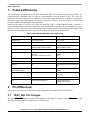
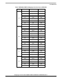
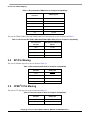
Freescale Semiconductor
AN2657
Rev. 1, 12/2004
Application Note
Designing a Universal PowerQUICC III
Board: MPC8560 and MPC8555
by
Kyle Aubrey
Field Applications Engineering, NCSG
San Jose, CA
Each processor in the PowerQUICC III family has unique features
targeted to interface with a particular price point and functionality
set. Because the 8555 and 8560 PowerQUICC III devices have the
same footprint, it is possible to design a single board to support
either of these PowerQUICC III processors. This allows a
universal board to support a wide variety of applications through
different component populations. For instance, a board populated
one way could support lower port count and lower power using a
MPC8555 at 533 MHz, but could be populated differently to
support a higher port count and higher performance using the
MPC8560 at 833 MHz. The result is lower fabrication costs and a
wider portfolio selection. Also, because devices in the
PowerQUICC III family have an e500 core and, in most cases, the
same peripherals, a single software package can be maintained for
the different builds of the same fabricated board.
This application note is intended to assist hardware and software
engineers in designing such a universal board—specifically for
the MPC8560 and the MPC8555—by providing the pin,
configuration, and register differences, as well as other
recommendations. The following topics are addressed:
© Freescale Semiconductor, Inc., 2004. All rights reserved.
PRELIMINARY—SUBJECT TO CHANGE WITHOUT NOTICE
1.
2.
3.
4.
5.
6.
7.
8.
9.
10.
11.
Contents
Feature Differences . . . . . . . . . . . . . . . . . . . . . . . . . . . 2
Pin Differences . . . . . . . . . . . . . . . . . . . . . . . . . . . . . . 2
One-to-One CPM Pin Mapping . . . . . . . . . . . . . . . . . 9
Configuration Differences . . . . . . . . . . . . . . . . . . . . 13
Port C External Interrupts Differences . . . . . . . . . . . 16
Register Differences . . . . . . . . . . . . . . . . . . . . . . . . . 17
Processor Identification . . . . . . . . . . . . . . . . . . . . . . 19
Board Identification . . . . . . . . . . . . . . . . . . . . . . . . . 19
Disabling Peripherals . . . . . . . . . . . . . . . . . . . . . . . . 20
Universal Schematic and Layout Symbol Creation . 20
Document Revision History . . . . . . . . . . . . . . . . . . . 20
Feature Differences
1
Feature Differences
The PowerQUICC III architecture of the MPC8560 and the MPC8555 integrates two processing blocks—the
high-performance embedded e500 core and the communications processor module (CPM). The e500 core
implements the Book E instruction set architecture and provides unprecedented levels of hardware and software
debugging support. The CPM supports a wide variety of protocols. However, as shown in Table 1, the MPC8555
provides a subset of the MPC8560's CPM capabilities.
Both processors offer a 256-Kbyte L2 cache, two integrated TSECs, a DDR SDRAM memory controller, a
programmable interrupt controller, I2C controllers, a four-channel DMA controller, and a general-purpose I/O port.
However, as Table 1 also shows, there are differences in the peripheral interfaces for PCI and RapidIO support. The
MPC8555 has an integrated hardware encryption block that is not supported by the MPC8560.
Table 1. MPC8560 and MPC8555 Feature Differences
Functionality
2
MPC8560
MPC8555
Fast Ethernet
FCC1, FCC2, FCC3
FCC1, FCC2
Gigabit Ethernet
TSEC1, TSEC2
TSEC1, TSEC2
Serial interfaces
TDMa1, TDMb1, TDMc1, TDMd1,
TDMa2, TDMb2, TDMc2, TDMd2
TDMa2, TDMb2, TDMc2
Max logical TDM channels
256 (128 per MCC)
64 (SCC in QMC mode)
ATM/UTOPIA L2
FCC1: 8/16b; FCC2: 8-bit
155 Mbps
AALx, AAL1 CES, IMA, TC Layer
FCC1 (8 bit), FCC2 (8 bit)
55-Mbps
AALx
SPI
1
1
I2C
2
2
USB 2.0
No
Muxed with SCC3—Low or full speed
only
Dedicated and non-dedicated
(SCCs/SMCs) UARTs
SCC1, SCC2, SCC3, SCC4
SCC1, SCC3, SCC4, SMC1, SMC2,
DUART
Security
No
IPSec, SSL/TLS, SRTP, 802.11i,
iSCSI, IKE
RapidIO
8-bit
No
PCI
Single 32-/64-bit PCI/PCI-X
Single 32-/64-bit PCI or
dual PCI (32 bit, 32 bit)
Pin Differences
Except where noted, this section lists different pin assignments from the MPC8560 to the MPC8555.
2.1
TEST_SEL Pin Changes
The AH20 TEST_SEL signal on the MPC8560 should be pulled high. This signal is named TEST_SEL0 on the
MPC8555 and should also be tied high with a 2–10 KΩ resistor.
Designing a Universal PowerQUICC III Board: MPC8560 and MPC8555, Rev. 1
2
PRELIMINARY—SUBJECT TO CHANGE WITHOUT NOTICE
Freescale Semiconductor
Pin Differences
The AG26 pin is a GND signal on the MPC8560, but it is TEST_SEL1 on the MPC8555 and should be tied to ground
through a 100-Ω–1-KΩ resistor. For a universal board, the MPC8560 should use a 0-Ω resistor to GND for this
signal to provide a population option for the 100-Ω–1-KΩ resistor for the MPC8555.
These changes are summarized in Table 2.
Table 2. MPC8560 to MPC8555 TEST_SEL Pin Changes
Pin Assignments
2.2
MPC8560
MPC8555
AH20
TEST_SEL
TEST_SEL0
2 Kbyte–10 Kbyte pull-up to OVdd 2 Kbyte–10 Kbyte pull-up to OVdd
AG26
GND
0 Ω resistor to GND
TEST_SEL1
100 Ω–1 KΩ resistor to GND
PCI Pin Changes
There are no changes if using the MPC8555 PCI1 interface as one 64-bit port or as one 32-bit port in synchronous
mode. However, the MPC8555 can also be configured to have two independent PCI-32 interfaces—PCI1 and PCI2.
The following sections describe changes in the pins when using the PCI2 features of the MPC8555.
2.2.1 No Connects (MPC8560) to Functional Pins (MPC8555)—No Changes
if Used the Same as MPC8560
Table 3 shows the differences between no-connect (N/C) pins in the MPC8560 and pin assignments in the MPC8555
using the PCI interface in asynchronous mode.
Table 3. MPC8560 No-Connects Mapping to MPC8555 PCI Signals
Pin
MPC8560 MPC8555
Comments
AF28
N/C
AVDD4
If PCI1 is disabled (DEVDISR[PCI1]=1) or is in synchronous mode, this signal can float
or be tied to VDD; in asynchronous mode, this signal must be tied to VDD. When tied
to VDD, the PLL power supply filter circuit (see Figure 1) should be implemented.
AE28
N/C
AVDD5
If PCI2 is disabled (DEVDISR[PCI2]=1) or is in synchronous mode, this signal can float
or be tied to VDD; in asynchronous mode, this signal must be tied to VDD. When tied
to VDD, the PLL power supply filter circuit (see Figure 1) should be implemented.
AH25
N/C
PCI1_CLK If PCI1 is disabled or is in synchronous mode, this signal can float or be tied to VDD;
if in asynchronous mode, connect to PCI clock.
AH27
N/C
PCI2_CLK If PCI2 is disabled or is in synchronous mode, this signal can float or be tied to VDD;
if in asynchronous mode, connect to PCI clock.
Figure 1 shows the PLL power supply filter circuit for AVDD when running in asynchronous PCI mode.
VDD
10 Ω
AVDD4 or AVDD5
2.2 µF
2.2 µF
GND
Low ESL Surface Mount Capacitors
Figure 1. PLL Power Supply Filter Circuit
Designing a Universal PowerQUICC III Board: MPC8560 and MPC8555, Rev. 1
Freescale Semiconductor
PRELIMINARY—SUBJECT TO CHANGE WITHOUT NOTICE
3
Pin Differences
2.2.2 PCI Pins (MPC8560) Changed to Dual PCI Functionality
(MPC8555)—No Changes if Used the Same as MPC8560
Table 4 shows the MPC8560 PCI signals that were renamed to implement the dual PCI functionality in the
MPC8555.
Table 4. PCI Signal Mapping—MPC8560 to MPC8555
Pin
MPC8560
MPC8555
Pin
MPC8560
MPC8555
AD13
PCI_ACK64
PCI2_DEVSEL
AD10
PCI_IRDY
PCI1_IRDY
Y14
PCI_PAR64
PCI2_PAR
W11
PCI_PERR
PCI1_PERR
AA11
PCI_PAR
PCI1_PAR
AF5
PCI_REQ0
PCI1_REQ0
AC13
PCI_AD0
PCI1_AD0
AF3
PCI_REQ1
PCI1_REQ1
AB13
PCI_AD1
PCI1_AD1
AE4
PCI_REQ2
PCI1_REQ2
W12
PCI_AD10
PCI1_AD10
AG4
PCI_REQ3
PCI1_REQ3
V12
PCI_AD11
PCI1_AD11
AE5
PCI_REQ4
PCI1_REQ4
AH11
PCI_AD12
PCI1_AD12
Y11
PCI_SERR
PCI1_SERR
AG11
PCI_AD13
PCI1_AD13
V11
PCI_STOP
PCI1_STOP
AF11
PCI_AD14
PCI1_AD14
AG10
PCI_TRDY
PCI1_TRDY
AE11
PCI_AD15
PCI1_AD15
AF18
PCI_AD32
PCI2_AD0
AA10
PCI_AD16
PCI1_AD16
AF17
PCI_AD33
PCI2_AD1
Y10
PCI_AD17
PCI1_AD17
AD16
PCI_AD42
PCI2_AD10
W10
PCI_AD18
PCI1_AD18
AC16
PCI_AD43
PCI2_AD11
AH9
PCI_AD19
PCI1_AD19
AB16
PCI_AD44
PCI2_AD12
Y13
PCI_AD2
PCI1_AD2
W16
PCI_AD45
PCI2_AD13
AG9
PCI_AD20
PCI1_AD20
V16
PCI_AD46
PCI2_AD14
AF9
PCI_AD21
PCI1_AD21
AH15
PCI_AD47
PCI2_AD15
AE9
PCI_AD22
PCI1_AD22
AG15
PCI_AD48
PCI2_AD16
AD9
PCI_AD23
PCI1_AD23
AD15
PCI_AD49
PCI2_AD17
AG8
PCI_AD24
PCI1_AD24
AC15
PCI_AD50
PCI2_AD18
AF8
PCI_AD25
PCI1_AD25
AB15
PCI_AD51
PCI2_AD19
AC8
PCI_AD26
PCI1_AD26
AE17
PCI_AD34
PCI2_AD2
AB8
PCI_AD27
PCI1_AD27
AA15
PCI_AD52
PCI2_AD20
AH7
PCI_AD28
PCI1_AD28
Y15
PCI_AD53
PCI2_AD21
AE7
PCI_AD29
PCI1_AD29
W15
PCI_AD54
PCI2_AD22
V13
PCI_AD3
PCI1_AD3
V15
PCI_AD55
PCI2_AD23
AD7
PCI_AD30
PCI1_AD30
AH14
PCI_AD56
PCI2_AD24
AH6
PCI_AD31
PCI1_AD31
AG14
PCI_AD57
PCI2_AD25
AH12
PCI_AD4
PCI1_AD4
AF14
PCI_AD58
PCI2_AD26
AG12
PCI_AD5
PCI1_AD5
AE14
PCI_AD59
PCI2_AD27
Designing a Universal PowerQUICC III Board: MPC8560 and MPC8555, Rev. 1
4
PRELIMINARY—SUBJECT TO CHANGE WITHOUT NOTICE
Freescale Semiconductor
Pin Differences
Table 4. PCI Signal Mapping—MPC8560 to MPC8555 (continued)
2.3
Pin
MPC8560
MPC8555
Pin
MPC8560
MPC8555
AE12
PCI_AD6
PCI1_AD6
AD14
PCI_AD60
PCI2_AD28
AD12
PCI_AD7
PCI1_AD7
AC14
PCI_AD61
PCI2_AD29
AB12
PCI_AD8
PCI1_AD8
AB17
PCI_AD35
PCI2_AD3
Y12
PCI_AD9
PCI1_AD9
AB14
PCI_AD62
PCI2_AD30
AC12
PCI_C/BE0
PCI1_C/BE0
AA14
PCI_AD63
PCI2_AD31
AD11
PCI_C/BE1
PCI1_C/BE1
AA17
PCI_AD36
PCI2_AD4
AB10
PCI_C/BE2
PCI1_C/BE2
Y17
PCI_AD37
PCI2_AD5
AH8
PCI_C/BE3
PCI1_C/BE3
W17
PCI_AD38
PCI2_AD6
AH10
PCI_DEVSEL
PCI1_DEVSEL
V17
PCI_AD39
PCI2_AD7
AC10
PCI_FRAME
PCI1_FRAME
AF16
PCI_AD40
PCI2_AD8
AE6
PCI_GNT0
PCI1_GNT0
AE16
PCI_AD41
PCI2_AD9
AG5
PCI_GNT1
PCI1_GNT1
W14
PCI_C/BE4
PCI2_C/BE0
AH5
PCI_GNT2
PCI1_GNT2
V14
PCI_C/BE5
PCI2_C/BE1
AF6
PCI_GNT3
PCI1_GNT3
AH13
PCI_C/BE6
PCI2_C/BE2
AG6
PCI_GNT4
PCI1_GNT4
AG13
PCI_C/BE7
PCI2_C/BE3
AA9
PCI_IDSEL
PCI1_IDSEL
AE13
PCI_REQ64
PCI2_FRAME
RapidIO Pins (MPC8560) Changed to Second 32-Bit PCI
Interface (MPC8555)
Table 5 shows which MPC8560 RapidIO pins were reassigned to implement the second 32-bit PCI interface in the
MPC8555. If the RapidIO interface is not used on the MPC8560, DEVDISR[RIO] should be set to disable the logic.
Table 5. MPC8560 RapidIO Pin Mapping to MPC8555 PCI Signals
Pin
MPC8560
MPC8555
AC18
RIO_TD1
PCI2_GNT0
AD18
RIO_TD0
PCI2_GNT1
AE18
RIO_TD0
PCI2_GNT2
AE19
RIO_TD1
PCI2_GNT3
AD19
RIO_TD2
PCI2_GNT4
AC22
RIO_TD6
PCI2_IDSEL
AD20
RIO_TD3
PCI2_IRDY
AC20
RIO_TCLK
PCI2_PERR
AD21
RIO_TD4
PCI2_REQ0
AE21
RIO_TCLK
PCI2_REQ1
Designing a Universal PowerQUICC III Board: MPC8560 and MPC8555, Rev. 1
Freescale Semiconductor
PRELIMINARY—SUBJECT TO CHANGE WITHOUT NOTICE
5
Pin Differences
Table 5. MPC8560 RapidIO Pin Mapping to MPC8555 PCI Signals (continued)
2.4
Pin
MPC8560
MPC8555
AD22
RIO_TD5
PCI2_REQ2
AE22
RIO_TD5
PCI2_REQ3
AC21
RIO_TD4
PCI2_STOP
AE20
RIO_TD3
PCI2_SERR
AC23
RIO_TD7
PCI2_REQ 4
AC19
RIO_TD2
PCI2_TRDY
CPM Pins (MPC8560) Changed to DUART Pins (MPC8555)
Table 6 shows which MPC8560 CPM pins were reassigned to implement the DUART interface in the MPC8555.
For reference, the last column of the table shows the pin assignments for the equivalent UART signals on the
MPC8560 using the SCCs. However, it should be noted that the CPM SCC UARTs programming model is different
than the DUART block of the MPC8555. For recommended CPM pin mux configurations for both the MPC8560
and MPC8555, see Section 3, “One-to-One CPM Pin Mapping.”
Table 6. MPC8560 CPM Pin Mapping to MPC8555 DUART Signals
2.5
Pin
MPC8560 CPM Port Name
MPC8555 DUART Name
Equivalent SCC UART
Signal (Pin Assignment)
Y1
pd4
UART_RTS0
pd29/SCC1_RTS (AD6)
Y2
pd5
UART_CTS0
pc15/SCC1_CTS (U9)
P11
pb14
UART_SIN0
pd31/SCC1_RXD (AE2)
N6
pb8/SCC3_TXD
UART_SOUT0
pd30/SCC1_TXD (AE3)
AD1
pd26/SCC2_RTS
UART_RTS1
—
Y3
pd6
UART_CTS1
pc13/SCC2_CTS (U7)
AD5
pd28/SCC2_RXD
UART_SIN1
—
AD2
pd27/SCC2_TXD
UART_SOUT1
—
CPM Pins (MPC8560) Changed to No-Connect (MPC8555)
Table 7 shows which MPC8560 CPM pins are reassigned as no-connects (N/C) on the MPC8555.
Designing a Universal PowerQUICC III Board: MPC8560 and MPC8555, Rev. 1
6
PRELIMINARY—SUBJECT TO CHANGE WITHOUT NOTICE
Freescale Semiconductor
Pin Differences
Table 7. MPC8560 CPM Pin Mapping to No-Connects on MPC8555
Port
Pin
MPC8560
MPC8555
J6
pa7
N/C
J5
pa6
N/C
J4
pa5
N/C
J3
pa4
N/C
J2
pa3
N/C
J1
pa2
N/C
H2
pa1
N/C
H1
pa0
N/C
P9
pb16
N/C
P10
pb15
N/C
N11
pb13
N/C
N10
pb12
N/C
N9
pb11
N/C
N8
pb10
N/C
N7
pb9
N/C
N5
pb7
N/C
N4
pb6
N/C
N1
pb5
N/C
M1
pb4
N/C
P8
pb1
N/C
Y9
pc31
N/C
W9
pc30
N/C
R11
pc3
N/C
R10
pc2
N/C
AA3
pd13
N/C
AA4
pd12
N/C
AA7
pd11
N/C
AA8
pd10
N/C
Y6
pd9
N/C
Y5
pd8
N/C
A
B
C
D
Designing a Universal PowerQUICC III Board: MPC8560 and MPC8555, Rev. 1
Freescale Semiconductor
PRELIMINARY—SUBJECT TO CHANGE WITHOUT NOTICE
7
Pin Differences
2.6
MPC8560 RapidIO Pins Changed to No-Connect (MPC8555)
Table 8 shows which MPC8560 RapidIO pins are reassigned as no-connects on the MPC8555. Note that if the
MPC8560’s RapidIO port is not used, it should be disabled with software by setting DEVDISR[RIO]. If disabled,
all RapidIO signals can be seen as N/Cs and left unterminated, saving valuable board space.
Table 8. MPC8560 RapidIO Pin Mapping to No-Connects on MPC8555
Pin
MPC8560
MPC8555
AF25
RIO_TX_CLK_IN
N/C
AF24
RIO_TX_CLK_IN
N/C
AE25
RIO_TFRAME
N/C
AE24
RIO_TFRAME
N/C
AE23
RIO_TD6
N/C
AD23
RIO_TD7
N/C
AE26
RIO_RFRAME
N/C
AE27
RIO_RFRAME
N/C
AD24
RIO_RD7
N/C
AC24
RIO_RD6
N/C
AB24
RIO_RD5
N/C
AA24
RIO_RD4
N/C
W24
RIO_RD3
N/C
V24
RIO_RD2
N/C
U24
RIO_RD1
N/C
T24
RIO_RD0
N/C
AD25
RIO_RD7
N/C
AC25
RIO_RD6
N/C
AB25
RIO_RD5
N/C
AA25
RIO_RD4
N/C
W25
RIO_RD3
N/C
V25
RIO_RD2
N/C
U25
RIO_RD1
N/C
T25
RIO_RD0
N/C
Y24
RIO_RCLK
N/C
Y25
RIO_RCLK
N/C
Designing a Universal PowerQUICC III Board: MPC8560 and MPC8555, Rev. 1
8
PRELIMINARY—SUBJECT TO CHANGE WITHOUT NOTICE
Freescale Semiconductor
One-to-One CPM Pin Mapping
3
One-to-One CPM Pin Mapping
Because some functionality and port pins have been removed from the MPC8555’s CPM, care should be taken in
selecting which pins to use to maintain functionality on the universal PowerQUICC III board when moving from
the MPC8560 to the MPC8555. This section describes which dedicated controller signals and serial interfaces are
identical for the MPC8560 and MPC8555.
3.1
FCC Pin Muxing
The logic for FCC3 and the 16-bit UTOPIA interface for FCC1 is not available with the MPC8555 CPM.
Additionally, the 8-bit UTOPIA interface pins on the FCC2 do not map one-to-one between the MPC8560 and
MPC8555, so it is recommended to only use FCC1 for the UTOPIA interface when designing a universal
PowerQUICC III board to support ATM. In summary, the interfaces that map one-to-one for FCC1 for both the
MPC8560 and MPC8555 are 8-bit UTOPIA for ATM, Fast Ethernet via RMII or MII, HDLC, and Transparent, as
shown in Table 9.
Table 9. Recommended FCC1 Pins for Footprint Compatibility
FCC1 NMSI
Port Pins
UTOPIA L2
8-Bit
MII
RMII
HDLC/
Transparent
pa25
TxD0
—
—
—
pa24
TxD1
—
—
—
pa23
TxD2
—
—
—
pa22
TxD3
—
—
—
pa21
TxD4
TxD3
—
TxD3
pa20
TxD5
TxD2
—
TxD2
pa19
TxD6
TxD1
TxD1
TxD1
pa18
TxD7
TxD0
TxD0
TxD0
pa10
RxD0
—
—
—
pa11
RxD1
—
—
—
pa12
RxD2
—
—
—
pa13
RxD3
—
—
—
pa14
RxD4
RxD3
—
RxD3
pa15
RxD5
RxD2
—
RxD2
pa16
RxD6
RxD1
RxD1
RxD1
pa17
RxD7
RxD0
RxD0
RxD0
pc15
TxADDR0
—
—
—
pc13
TxADDR1
—
—
—
pc7
TxADDR2
—
—
CTS
pd7
TxADDR3
—
—
—
pd19
TxADDR4
—
—
—
Designing a Universal PowerQUICC III Board: MPC8560 and MPC8555, Rev. 1
Freescale Semiconductor
PRELIMINARY—SUBJECT TO CHANGE WITHOUT NOTICE
9
One-to-One CPM Pin Mapping
Table 9. Recommended FCC1 Pins for Footprint Compatibility (continued)
FCC1 NMSI
Port Pins
UTOPIA L2
8-Bit
MII
RMII
HDLC/
Transparent
pc14
RxADDR0
—
—
—
pc12
RxADDR1
—
—
—
pc6
RxADDR2
—
—
CD
pd29
RxADDR3
—
—
—
pd18
RxADDR4
—
—
—
pa31
TxEnb
COL
—
—
pa28
RxEnb
TX_EN
TX_EN
—
pa30
TxClav
CRS
—
RTS
pa26
RxClav
RX_ER
RX_ER
—
pa29
TxSOC
TX_ER
—
—
pa27
RxSOC
RX_DV
CRS_DV
—
pd16, pc22
TxPrty
—
—
—
pd17, pc27
RxPrty
—
—
—
The interfaces for FCC2 are Fast Ethernet using MII or RMII, HDLC, and Transparent, as shown in Table 10.
Table 10. Recommended FCC2 Pins for Footprint Compatibility
FCC2 NMSI
Port Pins
MII
RMII
HDLC/
Transparent
pb27
COL
—
—
pb26
CRS
—
—
pb25
TxD3
—
TxD3
pb24
TxD2
—
TxD2
pb23
TxD1
TxD1
TxD1
pb22
TxD0
TxD0
TxD0
pb18
RxD3
—
RxD3
pb19
RxD2
—
RxD2
pb20
RxD1
RxD1
RxD1
pb21
RxD0
RxD0
RxD0
pb29
TX_EN
TX_EN
—
pb30
RX_DV
CRS_DV
—
pb31
TX_ER
—
—
pc4
—
—
CD
Designing a Universal PowerQUICC III Board: MPC8560 and MPC8555, Rev. 1
10
PRELIMINARY—SUBJECT TO CHANGE WITHOUT NOTICE
Freescale Semiconductor
One-to-One CPM Pin Mapping
Table 10. Recommended FCC2 Pins for Footprint Compatibility (continued)
3.2
FCC2 NMSI
Port Pins
MII
RMII
HDLC/
Transparent
pb28
RX_ER
RX_ER
RTS
pc5
—
—
CTS
SCC Pin Muxing
The logic for SCC2 is not available with the MPC8555 CPM. The pins for SCC1, SCC3, and SCC4 that map
one-to-one for the MPC8560 and MPC8555 are shown in Table 11.
Table 11. Recommended SCCx Pins for Footprint Compatibility
SCCx
NMSI Port Pins
UART/HDLC/Transparent
SCC1
pb28, pd30
TxD
pd31
RxD
pd29
RTS
pc29, pc15
CTS
pc14
CD
pd24
TxD
pd25
RxD
pd23
RTS
pc11, pc8
CTS
pc10
CD
pd21
TxD
pd22
RxD
pd20
RTS
pc9
CTS
pc8
CD
SCC3
SCC4
3.3
TDM Pin Muxing
MPC8560 and MPC8555 support multiple serial interfaces for dedicated TDM streams. The MPC8560 supports a
total of eight possible serial interfaces: TDMa1–TDMd1 and TDMa2–TDMd2, whereas the MPC8555 supports
only three: TDMa2, TDMb2, and TDMc2. For complete one-to-one mapping, only TDMa2 can be used. If L1RQ
and L1CLKO are not required, TDMc2 (MPC8560)/TDMb2 (MPC8555) can be used. However, it should be noted
that SIRAM register differences apply. Lastly, TDMc2 on the MPC8555 does not map to another TDM port on the
MPC8560. The pins for TDMa2 that map one-to-one for the MPC8560 and MPC8555 are shown in Table 12.
Designing a Universal PowerQUICC III Board: MPC8560 and MPC8555, Rev. 1
Freescale Semiconductor
PRELIMINARY—SUBJECT TO CHANGE WITHOUT NOTICE
11
One-to-One CPM Pin Mapping
Table 12. Recommended TDMa2 Pins for Footprint Compatibility
Serial Interface
Port Pins
TDMa2 Signals
pd22
L1TXD
pd21
L1RXD
pc9
L1TSYNC
pd20
L1RSYNC
pc1
L1RQ
pc0
L1CLKO
The pins for TDMc2 (MPC8560) and TDMb2 (MPC8555) that map one-to-one are shown in Table 13.
Table 13. Recommended TDMc2 (MPC8560)/TDMb2 (MPC8555) Pins for Footprint Compatibility
3.4
Serial Interface
Port Pins
TDMc2(8560)/TDMb2(8555)
Signals
pb27
L1TXD
pb26
L1RXD
pb25
L1TSYNC
pb24
L1RSYNC
SPI Pin Muxing
The pins for SPI that map one-to-one are shown in Table 14.
Table 14. Recommended SPI Pins for Footprint Compatibility
3.5
Port Pins
SPI Signals
pd19
SPISEL
pd18
SPICLK
pd17
SPIMOSI
pd16
SPIMISO
CPM I2C Pin Muxing
The pins for I2C that map one-to-one are shown in Table 15.
Table 15. Recommended I2C Pins for Footprint Compatibility
Port Pins
SPI Signals
pd15
I2CSDA
pd14
I2CSCL
Designing a Universal PowerQUICC III Board: MPC8560 and MPC8555, Rev. 1
12
PRELIMINARY—SUBJECT TO CHANGE WITHOUT NOTICE
Freescale Semiconductor
Configuration Differences
3.5.1 Banks of Clocks Mapping
The CPM provides for multiple clock sources into the PowerQUICC III device. The MPC8560 provides 20 possible
sources (CLK1–CLK20) whereas the MPC8555 provides 14 possible clock sources (CLK3–CLK16). When using
one-to-one mapped controllers with NMSI pin muxing, available clocks to each controller are the same. When using
the dedicated serial interfaces for TDM, there are exceptions to the available clock sources, as shown in Table 16.
Table 16. CLK Mapping for MPC8560 and MPC8555
MPC8555 Clock
MPC8560 Clock
Available
clock sources
TDMa2 Rx
TDMa2 Rx
CLK5, CLK13
TDMa2 Tx
TDMa2 Tx
CLK6, CLK14
TDMb2 Rx
TDMc2 Rx
CLK3
CLK17 is not available on the MPC8555
TDMb2 Tx
TDMc2 Tx
CLK4
CLK18 is not available on the MPC8555
TDMc2 Rx
—
CLK5, CLK13
TDMc2 Tx
—
CLK6, CLK14
Notes
Available clocks for TDMa2 are identical
Because the MPC8555 TDMc2 does not map to
another TDM interface on MPC8560, care should
be taken when using TDMc2 on the MPC8555.
Because TDMc2 of the MPC8560 maps directly to the TDMb2 of the MPC8555 as discussed in Section 3.3, “TDM
Pin Muxing,” the clock pins also map directly to each TDM interface as shown in Table 16.
4
Configuration Differences
Most POR configuration pins are the same between the MPC8560 and MPC8555; however there are a few
exceptions. Table 17 shows these exceptions in addition to all possible configurations. These differences are due
mostly to the differences in available peripheral blocks or relocation of configuration signals.
Table 17. POR Configuration Differences
Source
CCB Clock:
SYSCLK
Ratio
Configuration Signals
LA[28:31]
Reset Configuration
Name
cfg_sys_pll[0:3]
Value
(Binary)
Meaning
0010
2:1
0011
3:1
0100
4:1
0101
5:1
0110
6:1
1000
8:1
1001
9:1
1010
10:1
1100
12:1
0000
16:1
Designing a Universal PowerQUICC III Board: MPC8560 and MPC8555, Rev. 1
Freescale Semiconductor
PRELIMINARY—SUBJECT TO CHANGE WITHOUT NOTICE
13
Configuration Differences
Table 17. POR Configuration Differences (continued)
Source
e500 Core:
CCB Clock
Ratio
Boot ROM
Location
Configuration Signals
LALE, LGPL2
TSEC1_TXD[6:4]
(MPC8560)
Reset Configuration
Name
cfg_core_pll[0:1]
cfg_rom_loc[0:2]
LGPL0, LGPL1, LWE[3]
(MPC8555)
Host/Agent
LWE[2:3] (MPC8560)
LWE[2] (MPC8555)
CPU Boot
Boot
Sequencer
TSEC Width
TSEC1
Protocol
LA27
cfg_host_agt[0:1]
cfg_host_agt
cfg_cpu_boot
LGPL3, LGPL5
EC_MDC
TSEC1_TXD7 (MPC8560)
cfg_boot_seq[0:1]
cfg_tsec_reduce
cfg_tsec1
TSEC2_TXD3 (MPC8555)
TSEC2
Protocol
TSEC2_TXD7 (MPC8560)
TSEC2_TXD2 (MPC8555)
cfg_tsec2
Value
(Binary)
Meaning
00
2:1
01
2.5:1
10
3:1
11
3.5:1
000
PCI/PCI-X (MPC8560)
PCI 1 (MPC8555)
001
DDR SDRAM
010
PCI 2 (MPC8555)
011
RapidIO (MPC8560)
101
Local bus GPCM—8-bit ROM
110
Local bus GPCM—16-bit ROM
111
Local bus GPCM—32-bit ROM
(default)
00
PCI/PCI-X & RapidIO agent
01
RapidIO agent
10
PCI/PCI-X agent
11
Host for all (default)
0
PCI 1 Agent (MPC8555)
1
Host for all (default)
0
CPU boot hold off mode
1
Boot without waiting (default)
01
Normal I2C addressing
10
Extended I2C addressing
11
Boot sequencer disabled
(default)
0
Reduced mode: RTBI or RGMII
1
Standard mode: TBI or GMII
(default)
0
TSEC1: GMII or RGMII
1
TSEC1: TBI or RTBI (default)
0
TSEC2: GMII or RGMII
1
TSEC2: TBI or RTBI (default)
Designing a Universal PowerQUICC III Board: MPC8560 and MPC8555, Rev. 1
14
PRELIMINARY—SUBJECT TO CHANGE WITHOUT NOTICE
Freescale Semiconductor
Configuration Differences
Table 17. POR Configuration Differences (continued)
Source
Configuration Signals
RapidIO
LGPL0, LGPL1 (MPC8560)
Transmit
Clock Source
RapidIO
Device ID
Reset Configuration
Name
cfg_no_clk[0:1]
Value
(Binary)
Meaning
01
RapidIO RxCLK is source of
TxCLK
10
RapidIO TxCLK inputs are
source of TxCLK
11
CCB clock is source of TxCLK
(default)
TSEC2_TXD2 (MPC8560)
cfg_dev_ID5
x
Device ID for RapidIO hosts
TSEC2_TXD3 (MPC8560)
cfg_dev_ID6
x
Device ID for RapidIO hosts
TSEC2_TXD4 (MPC8560)
cfg_dev_ID7
x
Device ID for RapidIO hosts
PCI 1 Clock
Select
TSEC2_TXD1 (MPC8555)
cfg_pci1_clk
0
Async mode, PCI1_CLK used
1
Sync mode, SYSCLK used
(default)
PCI 2 Clock
Select
TSEC2_TXD0 (MPC8555)
0
Async mode, PCI2_CLK used
1
Sync mode, SYSCLK used
(default)
PCI Width
PCI_REQ64 (MPC8560)
0
PCI/PCI-X operates in 64-bit
mode (MPC8560)
PCI operates in 64-bit mode
(MPC8555)
1
PCI/PCI-X operates in 32-bit
mode (MPC8560) (default)
PCI operates as two 32-bit
interfaces (MPC8555) (default)
cfg_pci_impd
(MPC8560)
cfg_pci1_impd
(MPC8555)
0
25 Ω I/O drivers are used on the
PCI interface
1
42 Ω I/O drivers are used on the
PCI interface (default)
cfg_pci2_impd
0
25 Ω I/O drivers are used on the
PCI 2 interface
1
42 Ω I/O drivers are used on the
PCI 2 interface (default)
cfg_pci2_clk
cfg_pci_width
PCI1_REQ64/PCI2_FRAME
(MPC8555)
PCI I/O
Impedance
PCI_GNT1 (MPC8560)
PCI1_GNT1 (MPC8555)
PCI2_GNT1 (MPC8555)
PCI Arbiter
PCI Debug
PCI_GNT2 (MPC8560)
PCI1_GNT2 (MPC8555)
cfg_pci_arbiter
(MPC8560)
cfg_pci1_arbiter
(MPC8555)
0
PCI arbiter disabled
1
PCI arbiter enabled (default)
PCI2_GNT2 (MPC8555)
cfg_pci1_arbiter
0
PCI 2 arbiter disabled
1
PCI 2 arbiter enabled (default)
0
PCI debug is enabled
1
Normal PCI mode (default)
PCI_GNT3 (MPC8560)
PCI1_GNT3 (MPC8555)
cfg_pci_debug
Designing a Universal PowerQUICC III Board: MPC8560 and MPC8555, Rev. 1
Freescale Semiconductor
PRELIMINARY—SUBJECT TO CHANGE WITHOUT NOTICE
15
Port C External Interrupts Differences
Table 17. POR Configuration Differences (continued)
Source
PCI Debug
Configuration Signals
PCI_GNT3 (MPC8560)
Reset Configuration
Name
cfg_pci_debug
PCI1_GNT3 (MPC8555)
PCI-X
PCI_GNT4 (MPC8560)
Memory
Debug
MSRCID0
DDR Debug
MSRCID1
PCI Output
Hold
LWE[0:1] (MPC8560)
PCI1_GNT4 (MPC8555)
PCI2_GNT4 (MPC8555)
Local Bus
Output Hold
TSEC2_TXD[6:5]
(MPC8560)
cfg_pci_mode
cfg_mem_debug
cfg_ddr_debug
cfg_pci_hold[0:1]
cfg_pci1_hold
cfg_pci2_hold
cfg_lb_hold[0:1]
LWE[0:1] (MPC8555)
GeneralLAD[0:31]
Purpose POR
5
cfg_gpporcr
Value
(Binary)
Meaning
0
PCI debug is enabled
1
Normal PCI mode (default)
0
PCI-X mode
1
PCI mode (default)
0
LBC debug info driven
1
DDR debug info driven (default)
0
Debug info driven on ECC pins
1
Debug info is not driven on ECC
pins (default)
11
PCI: 2 buffer delays
PCI-X: 0 buffer delay
(default)
10
PCI: 3 buffer delays
PCI-X: 1 buffer delay
01
PCI: 0 buffer delay
PCI-X: 2 buffer delays
00
PCI: 1 buffer delay
PCI-X: 3 buffer delays
1
PCI1: 2 buffers delays (default)
0
PCI1: 0 buffer delay
1
PCI2: 2 buffers delays (default)
0
PCI2: 0 buffer delays
11
One buffer delay (default)
10
Two buffer delays
01
Three buffer delays
00
Zero buffer delays
xx
Vector placed in GPPORCR
Port C External Interrupts Differences
The MPC8560 has 16 potential external interrupts through the use of the CPM’s Port C. Since PC2 and PC3 are N/Cs
on the MPC8555, two potential interrupts had to be moved to another location in Port C: PC23 and PC29. However,
it should be noted that the priority levels of PC23 and 29 are higher than the rest of the external interrupts and not
the same as PC2 and PC3. The available interrupts and their priority levels are shown in Table 15. To maintain
interrupt priorities and pin compatibility, PC2, PC3, PC23, and PC29 should not be used for interrupts on a universal
PowerQUICC III board.
Designing a Universal PowerQUICC III Board: MPC8560 and MPC8555, Rev. 1
16
PRELIMINARY—SUBJECT TO CHANGE WITHOUT NOTICE
Freescale Semiconductor
Register Differences
Table 18. Port C External Interrupt Differences
6
CPM Priority Level
MPC8560 Interrupts
MPC8555 Interrupts
18 (Highest)
PC29
PC15
20
PC23
PC14
22
PC15
PC13
26
PC14
PC12
27
PC13
PC11
30
PC12
PC10
35
PC11
PC9
36
PC10
PC8
40
PC9
PC7
41
PC8
PC6
42
PC7
PC5
45
PC6
PC4
48
PC5
PC3
49
PC4
PC2
53
PC1
PC1
54 (Lowest)
PC0
PC0
Register Differences
Due to peripheral differences between the MPC8560 and MPC8555, certain register differences need to be
addressed. For instance, the MPC8555 has added registers for the second PCI port but has removed the RapidIO
registers. This section discusses other associated register and field differences between the two devices.
Additionally, note that any reserved field or area of memory should not be programmed; doing so could cause
unwanted behavior of the device. In most cases, reserved fields should be cleared when programming registers,
however this may not always be the case. The user should refer to the user manual for more information on proper
programming of reserved fields.
This section only covers the differences; common registers are not shown.
6.1
MPC8560-Only Registers
Table 19 indicates which registers are available only on the MPC8560, for those registers that are only available on
the MPC8555, refer to Table 20. Please note that there may be some fields in matching registers that are only
available for the MPC8560 or vice versa. The user should refer to the user manuals of both devices for a comparison
of these registers.
Designing a Universal PowerQUICC III Board: MPC8560 and MPC8555, Rev. 1
Freescale Semiconductor
PRELIMINARY—SUBJECT TO CHANGE WITHOUT NOTICE
17
Register Differences
Table 19. MPC8560-Only CCSR Registers
Register 1
Offset
0x8_0000–0x8_3FFF
DPRAM1–Dual Port RAM (16k)
0x8_8000–0x8_BFFF
DPRAM2–Dual Port RAM (16k)
0x9_1340–0x9_137F,
0x9_13D0–0x9_13FF
FCC3 Registers
0x9_1400–0x9_1414
TC layer 1 registers
0x9_1420–0x9_1434
TC layer 2 registers
0x9_1440–0x9_1454
TC layer 3 registers
0x9_1460–0x9_1474
TC layer 4 registers
0x9_1480–0x9_1494
TC layer 5 registers
0x9_14A0–0x9_14B4
TC layer 6 registers
0x9_14C0–0x9_14D4
TC layer 7 registers
0x9_14E0–0x9_14F4
TC layer 8 registers
0x9_1500–0x9_1503
TC layer–general registers
0x9_1A20–0x9_1A3F
SCC2 registers
0x9_1B00
CMXSI1CR–CPM Mux SI1 clock route register
0x9_1B20–0x9_1B2F
SI1 registers
0x9_1B30–0x9_1B3F
MCC1 registers
0x9_1B46
SI2DMR–SI2 TDMD2 mode register
0x9_1B50–0x9_1FFF
MCC2 registers
0x9_2000–0x9_27FF
SI1 RAM
0xA_0000–0xA_7FFF
IRAM–instruction RAM (32k)
0xC_0000–0x
RapidIO registers
1
6.2
See the MPC8560 Reference Manual for a full description of all associated registers.
MPC8555-Only Registers
Table 20 indicates which registers are only available only on the MPC8555; for those registers which are only
available on the MPC8560, refer to Table 19.
Table 20. MPC8555-Only CCSR Registers
Register 1
Offset
0x0_4500–0x 0_4511
UART0 registers
0x0_4600–0x0_4611
UART1 registers
0x0_9000–0x0_9FFC
PCI2 registers
0x3_0000–0x3_CFFF
Security engine registers
Designing a Universal PowerQUICC III Board: MPC8560 and MPC8555, Rev. 1
18
PRELIMINARY—SUBJECT TO CHANGE WITHOUT NOTICE
Freescale Semiconductor
Processor Identification
Table 20. MPC8555-Only CCSR Registers (continued)
Register 1
Offset
0x8_0000–0x8_1FFF
DPRAM1–dual port RAM (8 Kbytes)
0x8_8000–0x8_9FFF
DPRAM2–dual port RAM (8 Kbytes)
0x9_1A82–0x9_1A8F
SMC1 registers
0x9_1A92–0x9_1A9F
SMC2 registers
0x9_1B0C
CMXSMR–CPM Mux SMC clock route register
0x9_1B60–0x9_1FFF
USB registers
0xA_0000–0xA_0FFF
IRAM–instruction RAM (4 Kbytes)
1
7
See the MPC8555 Reference Manual for a full description of all associated registers.
Processor Identification
The revision codes in the processor version register (PVR) and the system version register (SVR) map to a particular
revision level marked on the device, as shown in Table 21. These registers can be accessed as SPRs through the e500
core or as memory-mapped registers. As such, a single software package can be created based on these registers that
supports not only multiple silicon revisions of the same PowerQUICC III processor by addressing certain errata
workarounds for a particular revision, but that also supports different members of the PowerQUICC III family.
The PVR identifies the version of the processor and the implementation of the version. Different version numbers
indicate major differences between processors, such as which optional facilities and instructions are supported.
Different revision numbers indicate minor differences between processors having the same version number, such as
clock rate and engineering change level.
The SVR identifies the version of the system logic and the implementation of the version. Different version numbers
indicate major differences in system logic. Different revision numbers indicate less significant changes in system
logic to address system logic errata or enhance certain features.
Table 21. Revision Level to Device Marking Cross-Reference
Silicon
Revision
8
e500 Core
Revision
Device Marking
Processor Version
Register (PVR)
System Version
Register (SVR)
PCI
DevID
MPC8560 Rev. 1
1.0
PPC8560PXxxxLA
0x8020_0010
0x8070_0010
0x09
MPC8560 Rev. 2
2.0
MPC8560PXxxxLB
0x8020_0020
0x8070_0020
0x09
MPC8555 Rev. 1
2.0
MPC8555PXxxxLA
0x8020_0010
0x8079_0010
0x0A
Board Identification
It is important to be able to identify the version of the board based on how it is populated. To do this, the version of
the board can be indicated through the use of the value found in the general-purpose POR configuration register
(GPPORCR). This value is sampled from the local bus address/data signals, LAD[0:31], during POR. Software can
use this value to inform the operating system about initial system configuration allowing software to not only disable
those features not used on the processor, but to also initialize all of the populated devices on that version of the board
using the same software package.
Designing a Universal PowerQUICC III Board: MPC8560 and MPC8555, Rev. 1
Freescale Semiconductor
PRELIMINARY—SUBJECT TO CHANGE WITHOUT NOTICE
19
Disabling Peripherals
Additionally, the POR configuration values of all device parameters sampled from pins at reset, such as PLL
multiplication values, are available through memory-mapped registers in the global utilities block.
9
Disabling Peripherals
The device disable register (DEVDISR) contains disable bits for various PowerQUICC III functional blocks. The
register is different between the MPC8560 and MPC8555 because available peripherals differ. All functional blocks
are enabled after reset; unneeded blocks can be disabled to reduce power consumption or allow their signals to be
used as general-purpose I/O signals. The disablement of these blocks can be based on either the system version
and/or the board version as mentioned in the previous two sections. Please note that blocks disabled by DEVDISR
must not be re-enabled without a hard reset.
10 Universal Schematic and Layout Symbol Creation
The MPC8560 and MPC8555 have identical footprints, so the same layout symbol may be used for both. It is
recommended that unified schematic symbols be created for both the MPC8560 and MPC8555 if both processors
are going to be used for the same fabricated board. If this is not feasible, the creation of two identical symbol blocks
with all NCs and Reserved pins shown should be created. Additionally, all signals listed in Section 2, “Pin
Differences,” should maintain the identical pin placement for creating visual compatibility in the schematic. To
obtain the schematic symbols for both the MPC8560 and MPC8555, contact your local Motorola salesperson or field
applications engineer (FAE). Symbols are available in Mentor Graphics®-compatible and EDIF formats.
11 Document Revision History
Table 22 provides a revision history for this application note.
Table 22. Revision History Table
Revision
Date
Substantive Change(s)
1
12/2004
Updated document template. In Table 5, changed pin assignments to PCI2_STOP = AC21and
PCI2_REQ4 = AC23
0
4/2004
Initial release
Designing a Universal PowerQUICC III Board: MPC8560 and MPC8555, Rev. 1
20
PRELIMINARY—SUBJECT TO CHANGE WITHOUT NOTICE
Freescale Semiconductor
Document Revision History
THIS PAGE INTENTIONALLY LEFT BLANK
Designing a Universal PowerQUICC III Board: MPC8560 and MPC8555, Rev. 1
Freescale Semiconductor
PRELIMINARY—SUBJECT TO CHANGE WITHOUT NOTICE
21
Document Revision History
THIS PAGE INTENTIONALLY LEFT BLANK
Designing a Universal PowerQUICC III Board: MPC8560 and MPC8555, Rev. 1
22
PRELIMINARY—SUBJECT TO CHANGE WITHOUT NOTICE
Freescale Semiconductor
Document Revision History
THIS PAGE INTENTIONALLY LEFT BLANK
Designing a Universal PowerQUICC III Board: MPC8560 and MPC8555, Rev. 1
Freescale Semiconductor
PRELIMINARY—SUBJECT TO CHANGE WITHOUT NOTICE
23
How to Reach Us:
Home Page:
www.freescale.com
email:
[email protected]
USA/Europe or Locations Not Listed:
Freescale Semiconductor
Technical Information Center, CH370
1300 N. Alma School Road
Chandler, Arizona 85224
(800) 521-6274
480-768-2130
[email protected]
Information in this document is provided solely to enable system and software implementers to
use Freescale Semiconductor products. There are no express or implied copyright licenses
Europe, Middle East, and Africa:
Freescale Halbleiter Deutschland GmbH
Technical Information Center
Schatzbogen 7
81829 Muenchen, Germany
+44 1296 380 456 (English)
+46 8 52200080 (English)
+49 89 92103 559 (German)
+33 1 69 35 48 48 (French)
[email protected]
granted hereunder to design or fabricate any integrated circuits or integrated circuits based on the
Japan:
Freescale Semiconductor Japan Ltd.
Technical Information Center
3-20-1, Minami-Azabu, Minato-ku
Tokyo 106-0047 Japan
0120 191014
+81 3 3440 3569
[email protected]
data sheets and/or specifications can and do vary in different applications and actual performance
Asia/Pacific:
Freescale Semiconductor Hong Kong Ltd.
Technical Information Center
2 Dai King Street
Tai Po Industrial Estate,
Tai Po, N.T., Hong Kong
+800 2666 8080
[email protected]
where personal injury or death may occur. Should Buyer purchase or use Freescale
For Literature Requests Only:
Freescale Semiconductor
Literature Distribution Center
P.O. Box 5405
Denver, Colorado 80217
(800) 441-2447
303-675-2140
Fax: 303-675-2150
LDCForFreescaleSemiconductor@
hibbertgroup.com
information in this document.
Freescale Semiconductor reserves the right to make changes without further notice to any
products herein. Freescale Semiconductor makes no warranty, representation or guarantee
regarding the suitability of its products for any particular purpose, nor does Freescale
Semiconductor assume any liability arising out of the application or use of any product or circuit,
and specifically disclaims any and all liability, including without limitation consequential or
incidental damages. “Typical” parameters which may be provided in Freescale Semiconductor
may vary over time. All operating parameters, including “Typicals” must be validated for each
customer application by customer’s technical experts. Freescale Semiconductor does not convey
any license under its patent rights nor the rights of others. Freescale Semiconductor products are
not designed, intended, or authorized for use as components in systems intended for surgical
implant into the body, or other applications intended to support or sustain life, or for any other
application in which the failure of the Freescale Semiconductor product could create a situation
Semiconductor products for any such unintended or unauthorized application, Buyer shall
indemnify and hold Freescale Semiconductor and its officers, employees, subsidiaries, affiliates,
and distributors harmless against all claims, costs, damages, and expenses, and reasonable
attorney fees arising out of, directly or indirectly, any claim of personal injury or death associated
with such unintended or unauthorized use, even if such claim alleges that Freescale
Semiconductor was negligent regarding the design or manufacture of the part.
Freescale™ and the Freescale logo are trademarks of Freescale Semiconductor, Inc. The
PowerPC name is a trademark of IBM Corp. and is used under license. All other product or service
names are the property of their respective owners.
© Freescale Semiconductor, Inc. 2004.
AN2657
Rev. 1
12/2004
PRELIMINARY—SUBJECT TO CHANGE WITHOUT NOTICE