1
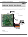
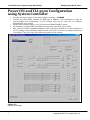
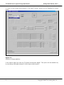
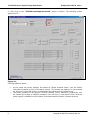
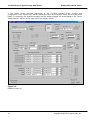
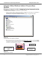
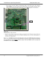
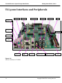
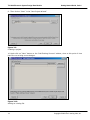
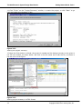
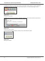
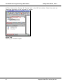
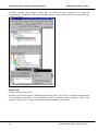
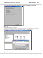
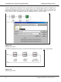
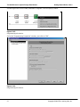
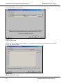
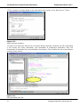
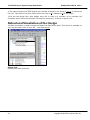
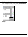
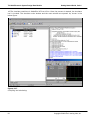
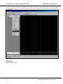
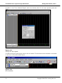
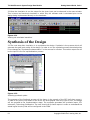
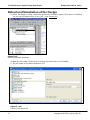
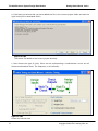
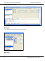
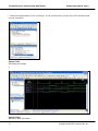
TLL5000
Electronic System Design
Base Module
Getting Started Guide, Ver 3.4
TLL5000 Electronic System Design Base Module
Getting Started Guide, Ver3.4
COPYRIGHT NOTICE
The Learning Labs, Inc. (“TLL”)
All rights reserved, 2008
Reproduction in any form without permission is prohibited.
Disclaimer
Information in this document is subject to change without notice and does not represent a
commitment on the part of TLL.
TLL provides this document as is, without warranty of any kind, expressed or implied,
including, but not limited to, the particular purpose. TLL may make improvements and/or
changes in this manual or in the products(s) and/or the program(s) described in this manual at
any time.
Information in this manual is intended to be accurate and reliable. However, TLL assumes no
responsibility for its use, or for any infringements of rights of other parties, which may result
from its use.
This document could include technical or typographical errors. Changes are periodically made
to the information herein; these changes may be incorporated in new editions of the
publication. This manual is provided solely and exclusively for educational use and this
information or related products should not be used nor relied upon for any purpose except for
education and training.
Technical Support
Please contact your local TLL authorized product representative for questions regarding
hardware, software or applications issues. Any updates or patches will be sent to you
automatically as long as your registration is current. The TLL products are designed to be
supported remotely by allowing viewing of the user’s desktop. It is highly recommended that
the PC from which you are using TLL products is connected to an Internet link that allows Web
browser access. In this way our technical support staff can view your desktop and work with
you to understand and solve technical issues
2
Copyright © 2008 The Learning Labs, Inc.
TLL5000 Electronic System Design Base Module
Getting Started Guide, Ver3.4
Table of Contents
Prerequisites .............................................................................................. 4
System Requirements ............................................................................... 4
Software requirements .............................................................................. 4
Hardware requirements ............................................................................. 4
Setting up TLL5000 Base Module ................................................................... 6
Power ON and TLL5000 Configuration using Hardware Manager ...................... 7
Setup for Xilinx Platform Cable & TLL5000 Base Module: .............................. 11
TLL5000 Interfaces and Peripherals ........................................................... 13
Digital Design using Xilinx ISE ..................................................................... 14
Functional Test on the TLL5000 ................................................................ 39
Digital Design Using VHDL .......................................................................... 40
Behavioral Simulation of the Design .......................................................... 48
Synthesis of the Design ........................................................................... 53
Implementation of the Design .................................................................. 54
Programming TLL5000 ............................................................................ 58
Functional Test on the TLL5000 ................................................................ 63
Digital Design Using Verilog HDL ................................................................. 64
Behavioral Simulation of the Design .......................................................... 74
Synthesis of the Design ........................................................................... 78
Implementation of the Design .................................................................. 79
Programming TLL5000 ............................................................................ 83
Functional Test on the TLL5000 ................................................................ 89
3
Copyright © 2008 The Learning Labs, Inc.
TLL5000 Electronic System Design Base Module
Getting Started Guide, Ver3.4
Chapter 1
Prerequisites
System Requirements
The following are the prerequisites for a computer to run the required software tools for doing
basic digital designs on theTLL5000. Make sure that these components and minimum hardware are
present.
•
•
•
•
•
•
•
•
•
Personal Computer: Pentium 1 GHz or higher -- Although lower processors will run the software
tools, the desired results are not guaranteed.
512MB RAM – for average applications, larger designs a 1GB RAM or greater is useful.
Minimum 5-GB on Hard Disk – The Webpack ISE requires around 3.5 GB for all its components.
DVD Drive
SVGA Monitor with the resolution of 1024x768 -- Monitor resolutions has been kept at
1024x768, which is ideal.
Windows 2000 or XP operating system with ServicePack-4 (for Windows 2000) & ServicePack-2
(for WinXP)
Three USB2.0 ports
One RS232 serial port
Ethernet Network Interface Card (NIC) The network interface card should have been configured
on your system. Make sure that you have configured the network card with a static IP address.
Software requirements
The following software needs to be installed in the PC used for connecting to the TLL5000 Base
Module.
• Xilinx Webpack ISE 9.x/ 10.x (our limited experience is that the Xilinx ISE version 8.x should
also work, but we recommend that you use version 9.x). If you are using the previous versions
of ISE, please update with the service packs for getting the drivers for the Xilinx Programming
Cable. This tool is provided with, ISE simulator, XST synthesizer, PAR and downloads (iMPACT)
applications.
• ModelSim-XE – the Simulation software for behavioral simulation. One should also be able to do
these exercises using the full ModelSim software from Mentor Graphics but there will be
differences in methods and commands that this manual does not address.
Hardware requirements
•
•
•
•
•
•
4
The following items are required to start using the system.
TLL5000 Base Module.
Power supply for TLL5000 (18volts / 3.5 Amps)
USB cables – 2 Nos.
Xilinx Platform Programming Cable – newer versions use an USB interface, but parallel cables
will also work.
CDs with, User Documentations and Software.
Copyright © 2008 The Learning Labs, Inc.
TLL5000 Electronic System Design Base Module
Getting Started Guide, Ver3.4
The CDs provided with the TLL5000 will typically contain the following items. Please consult
with your local TLL product partner for specific details as your configuration may be different from
this table.
DVD
1
2
Directory
Description
Remarks
TLL User Software
and Manuals
Various application utilities and
associated software and hardware
manuals for the TLL5000.
Web downloadable
software tools
As a convenience for the user, this
CD has the freely downloadable
FPGA software from the Xilinx
Website. The registration is done
online by the user.
Please check with your local
TLL partner to verify that the
manuals and software are the
most current versions.
These tools will have a license
duration determined by Xilinx
and they will provide updates
through their standard update
mechanisms.
Note1: The installation of Xilinx tools are self guided. Click on the Setup.exe in the directory and
the installation starts.
Note2: Choose the option of cable drivers during the installation of Webpack ISE. If these drivers
are not chosen then the drivers for Platform cable – USB will not be installed in the System.
5
Copyright © 2008 The Learning Labs, Inc.
TLL5000 Electronic System Design Base Module
Getting Started Guide, Ver3.4
Chapter 2
Setting up TLL5000 Base Module
The following picture shows the connections to be made between the PC and TLL5000 Base
Module. Please strictly follow the steps as per the manual to avoid any problems to the hardware.
The wrong sequence of applying power and connection sequence can cause damage to the system.
Power Supply
(18v / 3.5A)
Power ON/
OFF Switch
Power
Connector
(CON100)
USB port for TLL5000
Connection
(CON801)
USB Cable1
Xilinx Cable2
FPGA JTAG port
(CON1)
JTAG port
(From PC to TLL5000
14-pin CON1)
Figure 2-1
TLL5000 platform setup.
6
Copyright © 2008 The Learning Labs, Inc.
TLL5000 Electronic System Design Base Module
Getting Started Guide, Ver3.4
Power ON and TLL5000 Configuration
using System Controller
•
•
•
•
•
Connect the power supply to the power supply connector – CON100.
Connect the USB cable1 between PC-USB port & CON801. This connection is used for
communication and configuration of the TLL5000 from the PC using the TLL software
provided with your system.
Switch ON the power supply on the TLL5000 with POWER ON/OFF Switch.
As the power is switched ON, the LEDs near the power connector will turn ON.
Now use the TLL5000 Hardware Manager utility (typically included as a menu selection in
the TLL Design Center software, please consult your local TLL partner for specific directions)
to configure. This will bring up the following screen on the monitor.
Figure 2-2
Hardware Manager.
7
Copyright © 2008 The Learning Labs, Inc.
TLL5000 Electronic System Design Base Module
Getting Started Guide, Ver3.4
1. Click on the Choose device option in the step-5 screen, options will be displayed as shown
below:
Figure 2-3
Selection of target platform.
In the options above we shall see “TLL5000 Development Board”. This option will be enabled only
by connecting USB cable between TLL5000 base module and PC.
8
Copyright © 2008 The Learning Labs, Inc.
TLL5000 Electronic System Design Base Module
Getting Started Guide, Ver3.4
2. Now click on the “TLL5000 Development Board” option in Step-6. The following screen
appears on PC.
Figure 2-4
Checking platform status.
•
•
9
At this stage the screen displays the status as “Board Powered Down” (see the Status
information marked in blue in the above screen). This means the platform is not powered
up. Once the “Power ON” button is clicked then the platform will get powered up.
The power supplies for the various TLL5000 elements (FPGA, memories, peripherals, etc)
are started by clicking on POWER (marked in the red color) in the above screen. Now the
power supply is enabled for all the parts of the board and the screen is shown as below.
Copyright © 2008 The Learning Labs, Inc.
TLL5000 Electronic System Design Base Module
Getting Started Guide, Ver3.4
3. The above screen provides monitoring of the TLL5000 onboard power supplies and
configuration of the various user-settable parameters such as the system clocks shown in the lower
tables. For example, the expected voltages and the actual voltages will be displayed in the “Power
Values Monitor” section in the upper left of the display screen.
Figure 2-5
Platform power up.
10
Copyright © 2008 The Learning Labs, Inc.
TLL5000 Electronic System Design Base Module
Getting Started Guide, Ver3.4
Setup for Xilinx Platform Cable & TLL5000 Base
Module:
Note: Before connecting the Xilinx Platform Programming Cable from the PC to the target TLL5000,
it is required to complete all the steps of TLL5000 Power ON and Configuration using the
TLL5000 Hardware Manager as explained in the above section.
•
When the Xilinx Platform Programming Cable is plugged into the system, the hardware is
identified. This can be verified by right clicking on
My Computer Æ Properties Æ Hardware Æ Device Manager Æ Programming cables.
Figure 2-6
Checking status of the platform USB cable.
•
Now observe the color of the status LED on the Platform cable – USB box. It will be orange.
The status will remain orange till the other end of Platform cable – USB (a 14-pin Flat ribbon
connector) is connected to the TLL5000.
Status LED
14-pin FRC connector
goes to TLL 5000 board
CON1
This end goes to
PC USB port
Figure 2-7
Checking status checking.
11
Copyright © 2008 The Learning Labs, Inc.
TLL5000 Electronic System Design Base Module
•
Getting Started Guide, Ver3.4
Now connect the Xilinx Platform Programming Cable to the JTAG 14-pin FRC connector
labeled CON1 on the lower right of the TLL5000 (this is non-reversible connector with a
notch on the connector long side). Please refer to the following diagram for connections.
CON1
Figure 2-8
TLL5000 platform JTAG connector.
•
When the Xilinx Platform Programming Cable is connected to the TLL5000 the status LED of the
Platform Programming Cable will turn GREEN indicating that the JTAG communication is
successful with target board.
Note: If the TLL5000 Power ON and Configuration using the TLL5000 Hardware Manager
are not followed, then the reference voltage for JTAG will not be available on CON1 of TLL5000 and
the status LED will remain ORANGE. Until the status LED turns GREEN, the bit file cannot be
downloaded onto the target Platform.
12
Copyright © 2008 The Learning Labs, Inc.
TLL5000 Electronic System Design Base Module
Getting Started Guide, Ver3.4
TLL5000 Interfaces and Peripherals
Audio In
RS232
S Video Out
RGB IN
RGB OUT
LCD
Audio Out
PS2 Key
Board
Switches
PS2 Mouse
Ethernet &
USB
MIC In
VGA
S Video In
NTSC / PAL In
NTSC / PAL OUT
Figure 2-9
Various interfaces in TLL5000.
13
Copyright © 2008 The Learning Labs, Inc.
LEDs
TLL5000 Electronic System Design Base Module
Getting Started Guide, Ver3.4
Chapter 3
Digital Design using Xilinx ISE
In this section we will introduce the steps needed to create a digital design with the schematic
entry method of circuit design. Schematic entry is often a starting step in learning digital design
prior to the Hardware Description Language approach to digital design, but can also be used
concurrently with HDL approaches when a block diagram or circuit view is the most natural method
of specifying the design. Now let us start with a basic design.
1. Run the ISE application by double clicking on the shortcut icon for the ISE tool or selecting it
from your Programs menu.
Figure 3-1
Invoking Xilinx ISE.
2. When the tool is invoked the following windows will appear in the ISE tool.
Figure 3-2
XILINX welcome screen.
14
Copyright © 2008 The Learning Labs, Inc.
TLL5000 Electronic System Design Base Module
Getting Started Guide, Ver3.4
3. Now a new project has to be created. To create a new project, click on the “File” menu and
select “New Project” option.
Figure 3-3
Creating a new project.
4. When the new project option is selected the following window is seen. In this window type a
project name “buffer_sch” and specify a location. Select “Schematic” as the Top-Level Source Type.
And click “Next”.
Figure 3-4
Entering the project name.
15
Copyright © 2008 The Learning Labs, Inc.
TLL5000 Electronic System Design Base Module
Getting Started Guide, Ver3.4
5. After these inputs the tool will go to the next window. Here select the target device and the
tools that will be used in developing the design. Then click “Next”.
Figure 3-5
Selecting of a device.
6. In the next window, click on “New Source” tab. In the “New Source Wizard” window give the file
name and select the input file type as schematic.
Figure 3-6
Selecting a source type.
16
Copyright © 2008 The Learning Labs, Inc.
TLL5000 Electronic System Design Base Module
Getting Started Guide, Ver3.4
7. When the “Next” button is clicked, the “New Source Wizard” summary window will be seen.
Click on “Finish” here.
Figure 3-7
Completing the new source wizard.
8. In the next window click “Yes”, to create the new project directory.
Figure 3-8
Confirming the project creation.
17
Copyright © 2008 The Learning Labs, Inc.
TLL5000 Electronic System Design Base Module
Getting Started Guide, Ver3.4
9. Then click on “Next” in the “New Project Wizard”.
Figure 3-9
Creating a project.
10. Again click on “Next” button on the “Add Existing Sources” window, since at this point of time
there are no existing source designs.
Figure 3-10
Adding an existing file.
18
Copyright © 2008 The Learning Labs, Inc.
TLL5000 Electronic System Design Base Module
Getting Started Guide, Ver3.4
11. Click “Finish” on the “Project Summary” window, to create the project, or click “Back” to go
back and make some changes, if any.
Figure 3-12
Viewing the project summary.
12. Once the finish button is clicked, the project is created and the design summary is also given in
the ISE tool window, as shown below. And click on the file name tab to edit the file, as shown in
the red circle on the figure.
Figure 3-13
Viewing project summary in HTML format.
19
Copyright © 2008 The Learning Labs, Inc.
TLL5000 Electronic System Design Base Module
Getting Started Guide, Ver3.4
13. Click on the “Float Window” button to get a better view of the schematic editor. This is the
same as an undocking feature.
Figure 3-14
Undocking the window.
14. Once the schematic editor is undocked, i.e. the window is floated, the following window can be
observed.
Figure 3-15
Selecting the components.
In this window click on “Symbols” tab in order to get the various components under different
component categories, in the left side of the window.
20
Copyright © 2008 The Learning Labs, Inc.
TLL5000 Electronic System Design Base Module
Getting Started Guide, Ver3.4
15. From the “Categories” tab in left side of the window, select “buffer” and select the desired
symbol from the “Symbols” tab and place in the editor window, as shown in the figure. The editor
can be zoomed in / out as per the requirement. Notice the grid positions as guides to drawing a
neat layout.
Figure 3-16
Placing the components.
16. After placing the components, the wire has to be connected. To connect the wires right click in
the editor, select “Add” select “Wire”.
Figure 3-17
Adding wires to the components.
21
Copyright © 2008 The Learning Labs, Inc.
TLL5000 Electronic System Design Base Module
Getting Started Guide, Ver3.4
17. Now as shown in the below given figure, add the wires to the components, in the editor
window.
Figure 3-18
Placing wires.
18. After adding wires to the components, the IO markers are to be added to the wires, which
should be used for applying the inputs and monitoring the outputs. To add IO markers again right
click in the schematic editor, select “Add” and select “I/O Marker”.
Figure 3-19
Adding I/O marker.
22
Copyright © 2008 The Learning Labs, Inc.
TLL5000 Electronic System Design Base Module
Getting Started Guide, Ver3.4
19. Place the IO markers as shown in the figure. While placing the input marker select “Add an
input maker” and for the output marker “Add an output marker” in the options window on the left
hand side of the window.
Figure 3-20
Renaming I/O markers.
20. To edit the object properties of the IO markers, in the name field delete the existing name and
give the desired name, and click “OK”.
Figure 3-21
Renaming the markers.
23
Copyright © 2008 The Learning Labs, Inc.
TLL5000 Electronic System Design Base Module
Getting Started Guide, Ver3.4
21. Repeat the same for all the ports. Save the schematic. Next perform a “Check Schematic”
function has to be done. This same as check syntax process, in the text based design entries.
Figure 3-22
Checking the schematic.
22. Observe the “No error or warning is detected” message in the console window as shown below.
Figure 3-23
Observing console window.
23. Then dock the floating window by clicking on the “Dock Window” button.
Figure 3-24
Docking the window.
24
Copyright © 2008 The Learning Labs, Inc.
TLL5000 Electronic System Design Base Module
Getting Started Guide, Ver3.4
24. Then click on the “Sources” & “Process” tabs in the ISE tool window. Select the option as
“Behavioral Simulation” in the “Sources for” window.
Figure 3-25
Selecting the simulation option.
25
Copyright © 2008 The Learning Labs, Inc.
TLL5000 Electronic System Design Base Module
Getting Started Guide, Ver3.4
25. By selecting the input file name in the “Sources for” window, expand the “ModelSim Simulator”
window from the “Process for” window and run the process called “Simulate Behavioral Model”.
This will invoke the simulator that we use to simulate the design. Here ModelSim XE 6.2c is the
simulator used.
Figure 3-26
Forcing the input signals.
26. Force the selected input signals with the desired values, and click on “OK”.
Figure 3-27
Docking the window.
26
Copyright © 2008 The Learning Labs, Inc.
TLL5000 Electronic System Design Base Module
Getting Started Guide, Ver3.4
27. Then click on “Run” button, in order to view the simulated results.
Figure 3-28
Run simulation.
28. The simulated results can be seen in the wave form window. The vertical yellow bar is the
cursor. Wherever the cursor is placed, the corresponding values will be displayed in the wave
window, as marked in the below shown figure. Different inputs can be applied and the output can
be viewed accordingly. Once the satisfied output is got the simulator may be quitted.
Figure 3-29
Viewing the simulated output.
29. The next step in the FPGA design flow is to synthesize the design. Synthesis is the process that
generates the equivalent gate level netlist for the input design file. The netlist is a text based file
that contains the details of the devices and the interconnection network that are used in the
design.
30. In order to run the synthesize process, select “Synthesis/Implementation” option in the “Source
for” tab, and right click on the “Synthesize – XST” process, in “Process for” window and select
“Run” from the pop-up menu. Once the synthesis is completed, expand the synthesis process to
view the synthesis report, RTL Schematic & Technology view of the given design.
27
Copyright © 2008 The Learning Labs, Inc.
TLL5000 Electronic System Design Base Module
Getting Started Guide, Ver3.4
31. The above processes are shown below.
Figure 3-30
Synthesizing the design.
32. The next process is the implementation process. This process has three major steps under it.
They are (a) Translate, (b) Map and (c) Place And Route.
Translate:
Translate is the process that merges all the input files and the constraint file into a single netlist.
Map:
Map is the process that maps the logical components to the physical components. Logical
components are the ones which are there that according to the circuit diagram. And, the physical
components are the ones that are physically present inside the FPGA.
Place And Route (PAR):
The map output file will be taken as the input file for the PAR process. The map file will contain how
many CLBs & IOBs are required to implement the design. And also it will have the details of which
are the CLBs & IOBs that are used in the design implementation. Based on that information, those
particular CLBs and IOBs will be configured. This process is called as placing, and the routing is the
process which makes the interconnection CLBs and/or IOBs.
33. Before going to the process of implementation, it is necessary to write the user constraints
(ucf) file. This is the file where the designer can give the constraints for the design to be
implemented.
28
Copyright © 2008 The Learning Labs, Inc.
TLL5000 Electronic System Design Base Module
Getting Started Guide, Ver3.4
34. To enter an ucf file, click on “Project” menu and select “New Source” option.
Figure 3-31
Creating a new source for constraints file.
35. Once the new source is selected, the “New Source Wizard” window gets opened. Here, enter
the file name and select the input file type as “Implementation Constraints File” and click on
“Next”.
Figure 3-32
Synthesizing the design.
36. When the next button is clicked, the “Associate Source” window gets opened. Here select the
appropriate entity/file name. If only one file is added to the project, then by default the same is
selected. If more than one number files are there, only then we need to select the file/entity name.
29
Copyright © 2008 The Learning Labs, Inc.
TLL5000 Electronic System Design Base Module
Getting Started Guide, Ver3.4
37. Select the file (entity) name and click on “Next”.
Figure 3-33
Selecting an associated source.
38. Then again click on the “Finish” button. If any changes are to be made, click on “Back” and
make the required changes.
Figure 3-34
File summary.
30
Copyright © 2008 The Learning Labs, Inc.
TLL5000 Electronic System Design Base Module
Getting Started Guide, Ver3.4
39. When this is completed, the ucf file is created and added to the project. To check this click on
the + sign beside the input file name in the “Sources for” window. In this example design, the pin
constraints will be in the ucf.
Figure 3-35
Assigning pin numbers.
40. To give the pin constraints, select the ucf file and expand the “User Constraints” in the “Process
for” window, and run the process “Assign Package Pins”. This will invoke another XILINX – built in
tool called PACE (Pinout Area Constraint Editor).
41. Enter the pin numbers, where the inputs and the outputs are supposed to be connected. The
details of these pin numbers, may be found in the user manual.
42. After entering the pin numbers, the save the file and PACE tool may be exited.
43. Then again select the design file in the “Sources for” window.
31
Copyright © 2008 The Learning Labs, Inc.
TLL5000 Electronic System Design Base Module
Getting Started Guide, Ver3.4
44. The next step is to run the implementation process. So, right click on the “Implement Design”
process and select “Run” from the pop-up menu.
Figure 3-36
Implementing design.
45. During the project design of a digital system each process can be found in some of the following
states
Running – the process is in the running phase.
Up-to-date – Process is successfully executed without mistakes or warnings. If the rapport is in
this condition it means that it’s up to date although it could happen that the tasks covered with this
process have mistakes and warnings.
Warnings reported – the process is successfully executed but there are warnings.
Errors reported – the process is finished with at least one error.
Out-of-Date – signifies that there have been made some changes and that the process needs to
be done again.
No icon – In the case of, there is no any of these icons the process hasn't been started.
32
Copyright © 2008 The Learning Labs, Inc.
TLL5000 Electronic System Design Base Module
Getting Started Guide, Ver3.4
46. After the design implementation process is complete, the programming file needs to be created
to download into the FPGA to correctly configure it. To generate the programming file, run the
process called “Generate Programming File” from the “Process for” window.
Figure 3-37
Generating bit file.
This process will generate the programming file. i.e., the bit stream file will be generated. This is
the file that will be downloaded onto the FPGA.
Once the file is generated, the next step is to make the communication between the host system
and the target TLL5000.
33
Copyright © 2008 The Learning Labs, Inc.
TLL5000 Electronic System Design Base Module
Getting Started Guide, Ver3.4
47. Before starting this process, “Power ON” the board as given previously. To make the
communication, expand the “Generate Programming File” process and select the “Configure Device
(iMPACT) process.
Figure 3-38
Configuring the target device.
48. Before running the process “Generate Programming File” right click on “Generate Programming
File” and select “Properties”. In the properties window, select the “start up Options” and set the
value as “JTAG Clock” in order to avoid the warning messages in the future.
34
Copyright © 2008 The Learning Labs, Inc.
TLL5000 Electronic System Design Base Module
Getting Started Guide, Ver3.4
49. This opens another software tool called iMPACT. Click on “Finish” button, in this window.
Figure 3-39
Checking for boundary scan devices.
50. This process detects three different devices that are present on TLL5000 target. The “xcf32p” is
the flash device, “xc9572” is the CPLD device and “xc3s1500” is the FPGA device.
Figure 3-40
Selecting the target device.
35
Copyright © 2008 The Learning Labs, Inc.
TLL5000 Electronic System Design Base Module
Getting Started Guide, Ver3.4
51. The “Assign New Configuration File” is place where the programming file will be browsed to the
location and selected, by clicking on the “Open” button. But, here DO NOT!! Select or configure the
flash device and the CPLD. So, click on the “Bypass” button to bypass these components. And
finally when the FPGA is highlighted, select the generated bit file, and click “Open”.
Figure 3-41
Selecting the bit file.
52. After completing this process, the bit file will be selected for the FPGA, to be programmed.
Figure 3-42
Selecting the bit file.
36
Copyright © 2008 The Learning Labs, Inc.
TLL5000 Electronic System Design Base Module
Getting Started Guide, Ver3.4
53. Now right click on the FPGA, and select “Program” from the pop-up menu.
Figure 3-43
Programming the device.
54. In the “Programming Properties” window, just click on “OK”.
Figure 3-44
Programming the device.
37
Copyright © 2008 The Learning Labs, Inc.
TLL5000 Electronic System Design Base Module
Getting Started Guide, Ver3.4
55. The program status can be observed by the viewing the “Progress Dialog” box.
Figure 3-45
Downloading the file.
56. Once the device is program is downloaded, the “Program Succeeded” message appears.
Figure 3-46
Viewing status message.
38
Copyright © 2008 The Learning Labs, Inc.
TLL5000 Electronic System Design Base Module
Getting Started Guide, Ver3.4
Functional Test on the TLL5000
The design downloaded onto the TLL5000 is tested for correct functionality with the use of switches
and LEDs available on the target TLL5000.
LEDs
Figure 3-47
Observing the outputs.
As the switches are toggled to ON/OFF positions, if the design is functioning correctly then the
corresponding output LEDs will turn ON/OFF to match the switch positions.
39
Copyright © 2008 The Learning Labs, Inc.
TLL5000 Electronic System Design Base Module
Getting Started Guide, Ver3.4
Chapter 4
Digital Design Using VHDL
1. To invoke the ISE 9.1 tool, double click on the below shown icon, on your desktop.
Figure 4-1
Invoking XILINX tool.
2. Once the tool is invoked the below shown window will open.
Figure 4-2
Tool welcome screen.
40
Copyright © 2008 The Learning Labs, Inc.
TLL5000 Electronic System Design Base Module
Getting Started Guide, Ver3.4
3. To start a new project, click on “File” tab and select “New Project”. The same is shown in the
below figure 4-3.
Figure 4-3
Creating new project.
4. When “New Project” is selected a new window is opened as shown in the figure. In the “Project
Name” field enter the desired project name. Now, it can be observed that a folder is created with
the same name in the “Project Location” field. This is for keeping track of all the input & output
files in the same location.
Figure 4-4
Entering project name.
41
Copyright © 2008 The Learning Labs, Inc.
TLL5000 Electronic System Design Base Module
Getting Started Guide, Ver3.4
5. Let the “Top-Level Source Type” be as HDL itself. After giving the necessary inputs and clicking
on “Next” the next window appears. This is the place where the target hardware & necessary tools
are selected. Key in the inputs as per the requirements. Then click on “Next”.
ModelSim-XE VHDL
Figure 4-5
Selecting target hardware.
Note 1: The Simulator Chosen – ModelSim—XE, Synthesis Tool – XST (this is the built-in Webpack
ISE)
Note 2: The device, Package and speed are chosen based on the details of an FPGA chip on the
TLL5000.
XC3S1500-4fg676
XC
– Xilinx Component.
3S
– Device Family, in this example, it is Spartan 3 Family.
1500 – Device Gate density. As per this example, 1500 kilo gates are present in this chip.
-4
– Speed Grade.
FG
– Package type. Fine-pitch Ball Grid Array.
676 – Number of I/Os on the chip.
42
Copyright © 2008 The Learning Labs, Inc.
TLL5000 Electronic System Design Base Module
Getting Started Guide, Ver3.4
6. To create a new source, click on the “New Source” button.
Figure 4-6
Creating new source file.
7. When the “new source” button is clicked give a file name for the input source code, and select
the file type, from the left hand side list. In this example it is a VHDL module.
Figure 4-7
Selecting file type.
43
Copyright © 2008 The Learning Labs, Inc.
TLL5000 Electronic System Design Base Module
Getting Started Guide, Ver3.4
8. After giving the file name & file type, the input and output port list of the design has to be
given. Port list is the top level entity of the design. After giving the port names the directions of
the ports can also be entered as per the design requirement. If the port is a type of bus, that can
also be entered, along with the number of bits specifying the width of the bus.
Figure 4-8
Enter the port list.
Note: The Port names to be entered in the above window shall also be 1 bit for typical logical gate
implementations. In the above design we have taken an input port of 8-bits (0 to 7) & output port
of 8-bits (0 to 7).
44
Copyright © 2008 The Learning Labs, Inc.
TLL5000 Electronic System Design Base Module
Getting Started Guide, Ver3.4
9. After giving those details, click on “Next” & “Finish”.
Figure 4-9
File summary.
10. After clicking on Next, the tool will ask for the confirmation of creating a new folder. Simply
“Yes” can be clicked. This will create a folder named as the project name, in the specified location.
And based on the information that is given, a skeleton of the VHDL file is created which will have
all the declaration parts of the file. This is common for all the VHDL files.
Figure 4-10
Creating project directory.
45
Copyright © 2008 The Learning Labs, Inc.
TLL5000 Electronic System Design Base Module
Getting Started Guide, Ver3.4
11. Click on “Next” in this window.
Figure 4-11
Creating new source.
12. Since a new project is being created, it is not required to add any existing source at this point
of time. So, click on “Next”.
Figure 4-12
Adding existing file (if any).
46
Copyright © 2008 The Learning Labs, Inc.
TLL5000 Electronic System Design Base Module
Getting Started Guide, Ver3.4
13. The summary is created based on the information that is given so far. Now click on “Finish”.
Figure 4-13
Viewing project summary.
14. Figure 4-14 shows the VHDL file for, the given design. Normally, whenever the file is generated
it will contain the library declaration, port declaration & architecture declaration. Only the
functionality of the design has to be entered by the designer. This simplifies the job of the designer
and time is also saved.
Figure 4-14
Tool generated VHDL file.
47
Copyright © 2008 The Learning Labs, Inc.
TLL5000 Electronic System Design Base Module
Getting Started Guide, Ver3.4
In the above window the IEEE libraries are included by default, the design b <= a; is entered by
the user. This code will act as a buffer where the value of a is loaded to b (all the 8-bits).
15. As per the design flow, after design entry the 1st step is to simulate. So to simulate, the
simulation option has to be selected. The steps for selecting it, is shown in figure 4-15.
Behavioral Simulation of the Design
16. When the design is ready, choose the Behavioral Simulation option (This option is available on
your top left hand corner of your ISE – near Sources for)
Figure 4-15
Selecting simulate operation.
48
Copyright © 2008 The Learning Labs, Inc.
TLL5000 Electronic System Design Base Module
Getting Started Guide, Ver3.4
17. Then select the VHDL file in the source for window and run the “Simulate Behavioral Model
Function”. To run any process, select the appropriate process and press enter or double click the
process or right click on the process and select run option from the pop up menu.
Figure 4-16
Simulating the design.
49
Copyright © 2008 The Learning Labs, Inc.
TLL5000 Electronic System Design Base Module
Getting Started Guide, Ver3.4
18. The simulator used here is ModelSim-XE from Xilinx. Once the process is started, the simulator
tool is invoked. The simulator main window and the wave window are opened. As, shown in the
below figure.
Figure 4-17
Compiling and simulating.
50
Copyright © 2008 The Learning Labs, Inc.
TLL5000 Electronic System Design Base Module
Getting Started Guide, Ver3.4
19. Now maximize the wave window and right click on the input signal and select “Force” from the
pop-up menu.
Figure 4-18
Selecting Force option.
51
Copyright © 2008 The Learning Labs, Inc.
TLL5000 Electronic System Design Base Module
Getting Started Guide, Ver3.4
20. When in the “Force Selected Signal” enter the desired value for the input signal(s) and click
“OK”.
Figure 4-19
Forcing the input signals.
21. After forcing the input signal, click on the run button. The shortcut to the run button is encircled
in red color in the below shown figure.
Figure 4-20
Run simulation.
52
Copyright © 2008 The Learning Labs, Inc.
TLL5000 Electronic System Design Base Module
Getting Started Guide, Ver3.4
22. Once the simulation is run the output for the given input can be observed in the wave window.
This is known as functional simulation in which only the software code is simulated prior to the
design being implemented directly on the hardware.
Figure 4-21
Viewing the simulated waveform.
Synthesis of the Design
23. The next step after simulation is to synthesize the design. Synthesis is the process which will
generate the gate level netlist of the design. In order to run the synthesis process the selection has
to be changed as “Synthesis/Implementation” in the sources for window. This netlist output file will
be the input file for the implementation process.
Figure 4-22
Selecting synthesis option.
The progress of the Synthesis process will be shown in the console of the ISE (Left-down corner).
In case of any errors, the details of the errors will be displayed. With any type of error, the design
will not proceed to the Implementation stage. The synthesis generates the synthesis report, RTL
schematic, Technology Schematics. The user should verify these reports in order to understand the
actual logical circuitry that will be configured in the FPGA.
53
Copyright © 2008 The Learning Labs, Inc.
TLL5000 Electronic System Design Base Module
Getting Started Guide, Ver3.4
Implementation of the Design
24. The implementation process has three different sub-processes in it. They are Translate, Map,
and the third is Place & Route.
Translate:
This is the process that merges all the input files and the constraint file into a single netlist.
Map:
The process of mapping the logical components to the physical components is known as Map.
Logical components are nothing but the components that we have as per the design circuit
diagram. Physical components are the components that are there inside FPGA such as LUTs,
gates, flip-flops.
Place And Route:
This is the process of configuring the appropriate CLBs & IOBs inside the FPGA and
interconnecting them. Also known as, PAR.
25. To do the implementation process, the constraints file has to be given as another input file. To
create a new user constraint file (ucf), click on project from the ISE software and select new
source. Once that is completed the window shown below appears. Select implementation constraint
file and give the desired file in the file name field. Then click on “Next”, “Next” and “Finish”.
Figure 4-23
Applying input constraints.
54
Copyright © 2008 The Learning Labs, Inc.
TLL5000 Electronic System Design Base Module
Getting Started Guide, Ver3.4
26. The above process will create an ucf file and automatically add it to the project. By selecting
the ucf file in sources for window, “Run” “Assign Package Pins” process from Processes for window.
The details of the pin locations are for switches and LEDs available on TLL5000 board.
Figure 4-24
Assigning package pins.
55
Copyright © 2008 The Learning Labs, Inc.
TLL5000 Electronic System Design Base Module
Getting Started Guide, Ver3.4
27. Once “Assign Package Pins” process is run another built-in tool from ISE will be opened called
Pin-out Area Constraint Editor (PACE). Enter the pin numbers in the LOC field as shown in the
figure. The pin number details in the figure below (bottom-left window labeled “Design Object List
– I/O Pins”) are as needed for the TLL5000 LEDs and Switches.
Figure 4-25
Applying pin numbers.
28. After entering the pin numbers in the LOC field save the file and exit the PACE tool. Then in the
“Sources for” window in ISE select the VHD file and run the “Generating Programming File”
process. This process will generate the bit file which can be downloaded onto the FPGA.
56
Copyright © 2008 The Learning Labs, Inc.
TLL5000 Electronic System Design Base Module
Getting Started Guide, Ver3.4
This process will run all the other processes that are there, before the generation of the
programming file. An individual process may also be run separately.
Figure 4-26
Generating bit file.
57
Copyright © 2008 The Learning Labs, Inc.
TLL5000 Electronic System Design Base Module
Getting Started Guide, Ver3.4
Programming TLL5000
29. After completing “Generating Programming File” process, expand “Generating Programming
File” process tab in the “Process for” window and run “Configure Device iMPACT” process. When
this process is executed the target board has to be connected, with the appropriate cable
connections.
Figure 4-27
Configuring the target platform.
30. Once the “Configure Device iMPACT” process is run, the below shown below appears. In this
window, just click on “Finish”.
Figure 4-28
Welcome screen of iMPACT.
58
Copyright © 2008 The Learning Labs, Inc.
TLL5000 Electronic System Design Base Module
Getting Started Guide, Ver3.4
31. Once the “Finish” is clicked the iMPACT tool will detect the boundary scan devices on the target
TLL5000. Here “xcf32p” is a flash prom & “xc9572” is a CPLD. These devices will NOT!! be
programmed. Click “Bypass” on the following window.
Figure 4-29
Detecting boundary scan devices.
59
Copyright © 2008 The Learning Labs, Inc.
TLL5000 Electronic System Design Base Module
Getting Started Guide, Ver3.4
32. This window is to select the programming file for the CPLD. Since we are not going to program
that this can also be bypassed.
Figure 4-30
Selecting programming file.
60
Copyright © 2008 The Learning Labs, Inc.
TLL5000 Electronic System Design Base Module
Getting Started Guide, Ver3.4
33. The third window is for the FPGA. Please ensure that the FPGA is selected by being highlighted.
Then select the appropriate bit file and click on “Open”.
Figure 4-31
Selecting bit file.
61
Copyright © 2008 The Learning Labs, Inc.
TLL5000 Electronic System Design Base Module
Getting Started Guide, Ver3.4
34. Now it can be observed that the FPGA is selected with the given bit file.
Figure 4-32
Programming selection.
7. Right click on the FPGA that is “xc3s1500” and select program from the pop-up menu. Then the
below shown window appears. Click on “OK” in this window. This will download the bit file onto the
target device.
Figure 4-33
Viewing programming properties.
62
Copyright © 2008 The Learning Labs, Inc.
TLL5000 Electronic System Design Base Module
Getting Started Guide, Ver3.4
35. Once programming is successfully completed, the “Program Succeeded” message appears as
shown in the given figure.
Figure 4-34
Programming status.
Functional Test on the TLL5000
36. The design downloaded onto the TLL5000 is tested for correct functionality with the use of
switches and LEDs available on the target TLL5000.
LEDs
Figure 4-35
Observing outputs.
As the switches are toggled to ON/OFF positions, if the design is functioning correctly then the
corresponding output LEDs will turn ON/OFF to match the switch positions.
63
Copyright © 2008 The Learning Labs, Inc.
TLL5000 Electronic System Design Base Module
Getting Started Guide, Ver3.4
Chapter 5
Digital Design Using Verilog HDL
1. To invoke the ISE 9.1 tool, double click on the below shown icon, on your desktop.
Figure 5-1
Invoking XILINX tool.
2. Once the tool is invoked the below shown window will open.
Figure 5-2
Tool welcome screen.
64
Copyright © 2008 The Learning Labs, Inc.
TLL5000 Electronic System Design Base Module
Getting Started Guide, Ver3.4
3. To start a new project, click on “File” tab and select “New Project”. The same is shown in
the below figure 5-3.
Figure 5-3
Creating new project.
4. When “New Project” is selected a new window is opened as shown in the figure. In the
“Project Name” field enter the desired project name. Now, it can be observed that a folder is
created with the same name in the “Project Location” field. This is for keeping track of all
the input & output files in the same location.
Figure 5-4
Entering project name.
65
Copyright © 2008 The Learning Labs, Inc.
TLL5000 Electronic System Design Base Module
Getting Started Guide, Ver3.4
5. Let the “Top-Level Source Type” be as HDL itself. After giving the necessary inputs and
clicking on “Next” the next window appears. This is the place where the target hardware &
necessary tools are selected. Key in the inputs as per the requirements. Then click on
“Next”.
Figure 5-5
Selecting target hardware.
Note 1: The Simulator Chosen –ISE Simulator, Synthesis Tool – XST (this is the built-in Webpack
ISE)
Note 2: The device, Package and speed are chosen based on the details of an FPGA chip on the
TLL5000.
XC3S1500-4fg676
XC
– Xilinx Component.
3S
– Device Family, in this example, it is Spartan 3 Family.
1500 – Device Gate density. As per this example, 1500 kilo gates are present in this chip.
-4
– Speed Grade.
FG
– Package type. Fine-pitch Ball Grid Array.
676 – Number of I/Os on the chip.
66
Copyright © 2008 The Learning Labs, Inc.
TLL5000 Electronic System Design Base Module
Getting Started Guide, Ver3.4
6. To create a new source, click on the “New Source” button.
Figure 5-6
Creating new source file.
7. When the “new source” button is clicked give a file name for the input source code, and
select the file type, from the left hand side list. In this example it is a VERILOG HDL module.
Figure 5-7
Selecting file type.
67
Copyright © 2008 The Learning Labs, Inc.
TLL5000 Electronic System Design Base Module
Getting Started Guide, Ver3.4
8. After giving the file name & file type, the input and output port list of the design has to be
given. Port list is the top level entity of the design. After giving the port names the
directions of the ports can also be entered as per the design requirement. If the port is a
type of bus, that can also be entered, along with the number of bits specifying the width of
the bus.
Figure 5-8
Enter the port list.
Note: The Port names to be entered in the above window shall also be 1 bit for typical logical gate
implementations.
68
Copyright © 2008 The Learning Labs, Inc.
TLL5000 Electronic System Design Base Module
Getting Started Guide, Ver3.4
9. After giving those details, click on “Next” & “Finish”.
Figure 5-9
File summary.
69
Copyright © 2008 The Learning Labs, Inc.
TLL5000 Electronic System Design Base Module
Getting Started Guide, Ver3.4
10. After clicking on Next, the tool will ask for the confirmation of creating a new folder. Simply
“Yes” can be clicked. This will create a folder named as the project name, in the specified
location. And based on the information that is given, a skeleton of the VERILOG HDL file is
created which will have all the declaration parts of the file. This is common for all the
VERILOG HDL files.
Figure 5-10a
Verilog file Summary
70
Copyright © 2008 The Learning Labs, Inc.
TLL5000 Electronic System Design Base Module
Getting Started Guide, Ver3.4
Figure 5-11
Creating project directory.
11. Click on “Next” in this window.
Figure 5-12
Creating new source.
71
Copyright © 2008 The Learning Labs, Inc.
TLL5000 Electronic System Design Base Module
Getting Started Guide, Ver3.4
12. Since a new project is being created, it is not required to add any existing source at this
point of time. So, click on “Next”.The summary is created based on the information that is
given so far. Now click on “Finish”.
Figure 5-13
Viewing project summary.
72
Copyright © 2008 The Learning Labs, Inc.
TLL5000 Electronic System Design Base Module
Getting Started Guide, Ver3.4
13. Figure 5-14 shows the VERILOG HDL file for, the given design. Normally, whenever the file
is generated it will contain, port declaration. Only the functionality of the design has to be
entered by the designer. This simplifies the job of the designer and time is also saved.
Figure 5-14
Tool generated Verilog HDL file.
In the above code the functionality for Sum and Cary out are written.
14. As per the design flow, after design entry the 1st step is to simulate. So to simulate, the
simulation option has to be selected. The steps for selecting it, is shown in figure 5-15.
73
Copyright © 2008 The Learning Labs, Inc.
TLL5000 Electronic System Design Base Module
Getting Started Guide, Ver3.4
Behavioral Simulation of the Design
15. When the design is ready, choose the Behavioral Simulation option (This option is available
on your top left hand corner of your ISE – near Sources for)
Figure 5-15
Selecting simulate operation.
16. Now we will create a Test bench for testing the functionality of a full adder.
a. We will create a Test bench Waveform file.
Figure 5 -16a
Create a Test bench file
74
Copyright © 2008 The Learning Labs, Inc.
TLL5000 Electronic System Design Base Module
Getting Started Guide, Ver3.4
b. Click Next and ensure that you have added the file in the current project folder and also the
right Verilog file is associated with it.
Figure 5-16b
Test bench file added to the current project directory
c. Now choose the type of clock. Since we are implementing a combinational circuit we will
choose combinational clock. The frequency is set internally.
Figure 5-16c
Chose the internal clock
75
Copyright © 2008 The Learning Labs, Inc.
TLL5000 Electronic System Design Base Module
Getting Started Guide, Ver3.4
d. Set the inputs as shown below.
Figure 5-16d
Set the inputs
e. From the Sources menu choose Behavior modeling option.
Figure 5-16e
Behavior modeling
76
Copyright © 2008 The Learning Labs, Inc.
TLL5000 Electronic System Design Base Module
Getting Started Guide, Ver3.4
f. Choose the appropriate file for simulating. In the process menu choose Xilinx ISE Simulator and
run the simulation.
Figure 5-16f
Simulating the design
g.
Figure 5-16g
Waveform after Simulation
77
Copyright © 2008 The Learning Labs, Inc.
TLL5000 Electronic System Design Base Module
Getting Started Guide, Ver3.4
Synthesis of the Design
17. The next step after simulation is to synthesize the design. Synthesis is the process which
will generate the gate level netlist of the design. In order to run the synthesis process the
selection has to be changed as “Synthesis/Implementation” in the sources for window. This
netlist output file will be the input file for the implementation process.
Figure 17
Selecting synthesis option.
The progress of the Synthesis process will be shown in the console of the ISE (Left-down corner).
In case of any errors, the details of the errors will be displayed. With any type of error, the design
will not proceed to the Implementation stage. The synthesis generates the synthesis report, RTL
schematic, Technology Schematics. The user should verify these reports in order to understand the
actual logical circuitry that will be configured in the FPGA.
78
Copyright © 2008 The Learning Labs, Inc.
TLL5000 Electronic System Design Base Module
Getting Started Guide, Ver3.4
Implementation of the Design
18. The implementation process has three different sub-processes in it. They are Translate,
Map, and the third is Place & Route.
Translate:
This is the process that merges all the input files and the constraint file into a single netlist.
Map:
The process of mapping the logical components to the physical components is known as Map.
Logical components are nothing but the components that we have as per the design circuit
diagram. Physical components are the components that are there inside FPGA such as LUTs,
gates, flip-flops.
Place And Route:
This is the process of configuring the appropriate CLBs & IOBs inside the FPGA and
interconnecting them. Also known as, PAR.
19. To do the implementation process, the constraints file has to be given as another input file.
To create a new user constraint file (ucf), click on project from the ISE software and select
new source. Once that is completed the window shown below appears. Select
implementation constraint file and give the desired file in the file name field. Then click on
“Next”, “Next” and “Finish”.
Figure 5-18
Applying input constraints.
79
Copyright © 2008 The Learning Labs, Inc.
TLL5000 Electronic System Design Base Module
Getting Started Guide, Ver3.4
20. The above process will create an ucf file and automatically add it to the project. By selecting
the ucf file in sources for window, “Run” “Assign Package Pins” process from Processes for
window. The details of the pin locations are for switches and LEDs available on TLL5000
board.
Figure 5-19
Assigning package pins.
21. Once “Assign Package Pins” process is run another built-in tool from ISE will be opened
called Pin-out Area Constraint Editor (PACE). Enter the pin numbers in the LOC field as
shown in the figure. The pin number details in the figure below (bottom-left window labeled
“Design Object List – I/O Pins”) are as needed for the TLL5000 LEDs and Switches.
80
Copyright © 2008 The Learning Labs, Inc.
TLL5000 Electronic System Design Base Module
Getting Started Guide, Ver3.4
Figure 5-20
Applying pin numbers.
22. After entering the pin numbers in the LOC field save the file and exit the PACE tool. Then in
the “Sources for” window in ISE select the V file and run the “Generating Programming File”
process. This process will generate the bit file which can be downloaded onto the FPGA.
81
Copyright © 2008 The Learning Labs, Inc.
TLL5000 Electronic System Design Base Module
Getting Started Guide, Ver3.4
This process will run all the other processes that are there, before the generation of the
programming file. An individual process may also be run separately.
Figure 5-21
Generating bit file.
82
Copyright © 2008 The Learning Labs, Inc.
TLL5000 Electronic System Design Base Module
Getting Started Guide, Ver3.4
Programming TLL5000
23. After completing “Generating Programming File” process, expand “Generating Programming
File” process tab in the “Process for” window and run “Configure Device iMPACT” process.
When this process is executed the target board has to be connected, with the appropriate
cable connections.
Figure 5-22
Configuring the target platform.
24. Once the “Configure Device iMPACT” process is run, the below shown below appears. In this
window, just click on “Finish”.
Figure 5-23
Welcome screen of iMPACT.
83
Copyright © 2008 The Learning Labs, Inc.
TLL5000 Electronic System Design Base Module
Getting Started Guide, Ver3.4
25. Once the “Finish” is clicked the iMPACT tool will detect the boundary scan devices on the
target TLL5000. Here “xcf32p” is a flash prom & “xc9572” is a CPLD. These devices will
NOT!! be programmed. Click “Bypass” on the following window.
Figure 5-24
Detecting boundary scan devices.
84
Copyright © 2008 The Learning Labs, Inc.
TLL5000 Electronic System Design Base Module
Getting Started Guide, Ver3.4
26. This window is to select the programming file for the CPLD. Since we are not going to
program that this can also be bypassed.
Figure 5-25
Selecting programming file.
85
Copyright © 2008 The Learning Labs, Inc.
TLL5000 Electronic System Design Base Module
Getting Started Guide, Ver3.4
27. The third window is for the FPGA. Please ensure that the FPGA is selected by being
highlighted. Then select the appropriate bit file and click on “Open”.
Figure 5-26
Selecting bit file.
28. Now it can be observed that the FPGA is selected with the given bit file.
Figure 5-27
Programming selection.
86
Copyright © 2008 The Learning Labs, Inc.
TLL5000 Electronic System Design Base Module
Getting Started Guide, Ver3.4
Right click on the FPGA that is “xc3s1500” and select program from the pop-up menu. Then the
below shown window appears. Click on “OK” in this window. This will download the bit file onto the
target device.
Figure 5-28
Viewing programming properties.
87
Copyright © 2008 The Learning Labs, Inc.
TLL5000 Electronic System Design Base Module
Getting Started Guide, Ver3.4
29. Once programming is successfully completed, the “Program Succeeded” message appears
as shown in the given figure.
Figure 5-34
Programming status.
88
Copyright © 2008 The Learning Labs, Inc.
TLL5000 Electronic System Design Base Module
Getting Started Guide, Ver3.4
Functional Test on the TLL5000
30. The design downloaded onto the TLL5000 is tested for correct functionality with the use of
switches and LEDs available on the target TLL5000.
Carry_output_led_2
Sum_output_led_1
Data_input_sw_1
Data_input_sw_2
Carry_in_sw_3
Figure 5-35
Observing outputs.
As the switches are toggled to ON/OFF positions, if the design is functioning correctly then the
corresponding output LEDs will indicate the Sum and Carry bits.
*END*
89
Copyright © 2008 The Learning Labs, Inc.