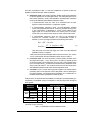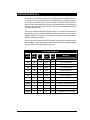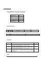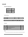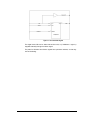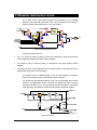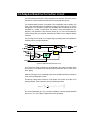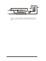
1
TPC ELECTRONICS S-ALTRO prototype Last Modified: 27.07.2010 INDEX Introduction _____________________________________________________ 4 Chapter 1.- Funtional Description ___________________________________ 5 1.1 Introduction _____________________________________________________5 1.2 Charge Shaping Amplifier __________________________________________8 1.3 Analogue to Digital Conversion _____________________________________9 1.4 First Baseline Correction _________________________________________10 1.5 Digital Shaper ___________________________________________________12 1.6 Baseline Correction and Subtraction II ______________________________14 1.7 Zero Suppression _______________________________________________16 1.8 Data Format ____________________________________________________18 1.9 Multi-Event Buffer _______________________________________________20 1.10 Trigger Handling ________________________________________________21 Chapter 2.- Mode of Use and Operation _____________________________ 22 2.1 Introduction ____________________________________________________22 2.2 Front-end Signals _______________________________________________23 2.3 ALTRO bus Signals ______________________________________________24 2.4 Instruction set __________________________________________________27 2.5 Register set ____________________________________________________29 2.6 Registers set ___________________________________________________54 2.7 Command Set ___________________________________________________57 2.8 Control Protocol_________________________________________________58 2.9 Modes of Use and Operation ______________________________________61 2.10 Digital Block Testability __________________________________________63 Chapter 3.- Circuit Description ____________________________________ 64 3.1 Introduction ____________________________________________________64 3.2 Analogue Front-end ______________________________________________65 3.3 Baseline Subtraction circuit _______________________________________70 3.4 Tail Cancellation Filter circuit______________________________________72 3.5 Adaptive Baseline Correction circuit _______________________________ 73 3.6 Zero Suppression circuit _________________________________________ 75 3.7 Data Format circuit ______________________________________________ 76 3.8 Multi-Event Buffer circuit _________________________________________ 77 3.9 Hamming State Machines _________________________________________ 79 Chapter 4.- Physical Description __________________________________ 81 4.1 Introduction ____________________________________________________ 81 4.2 Chip Layout and Pinout __________________________________________ 82 4.1 List of pins _____________________________________________________ 84 4.2 Power supply domains ___________________________________________ 90 4.3 Package Description _____________________________________________ 91 Chapter 5.- References __________________________________________ 92 Introduction The S-ALTRO prototype chip is a mixed-signal integrated circuit designed to be one of the building blocks of the readout electronics for gas detectors. Its architecture is based in the ALTRO (ALICE TPC Read Out) chip, being its main difference the integration of the charge shaping amplifier in the same IC. Just like ALTRO chip, the prototype architecture and programmability make it suitable for the readout of a wider class of detectors. In one single chip, 16 analogue signals from the detector are shaped, digitised, processed, compressed and stored in a multi-acquisition memory. The Analogue-to-Digital converters embedded in the chip have a 10-bit dynamic range and a maximum sampling rate up to 40MHz. After digitisation, a pipelined Data Processor is able to remove from the input signal a wide range of perturbations, related to the nonideal behaviour of the detector, temperature variation of the electronics, environmental noise, etc. Moreover, the Data Processor is able to suppress the pulse tail within 1μs after the peak with 1‰ accuracy, in order to improve their identification. The signal is then compressed by removing all data below a programmable threshold, except for a specified number of pre- and post-samples around each peak. This produces non-zero data packets. Eventually, each data packet is marked with its time stamp and size - so that the original data can be reconstructed afterwards - and stored in the multi-acquisition memory that has a readout bandwidth of 300Mbyte/sec. This document addresses the algorithms, the circuital implementation, the mode of use and operation, the physical implementation and performance of the S-ALTRO prototype. Chapter 1 Functional Description 1.1 Introduction The S-ALTRO prototype is a mixed analogue-digital custom integrated circuit dedicated to the shaping, digitisation and processing of gaseous detector signals. It contains 16 channels operating concurrently on the analogue signals coming directly from the detector. Upon arrival of a first level trigger, each input signal is shaped, sampled, processed and stored in a data memory. The maximum number of samples that can be continuously processed for each trigger (data stream) is 1008. When a second level trigger (accept) is received the data stream is either frozen in the Multi-Event Buffer (MEB), till its complete readout takes place, or discarded. The data memory has the capacity to store 8 data streams. As shown in figure 1.1, after the analogue to digital conversion, the signal processing is performed in 5 steps: a first correction and subtraction of the signal baseline, the digital shaping to, for example, cancel long-term components of the signal tail, a second baseline correction, the suppression of the samples so close to the baseline that contain no useful information (zero suppression), and formatting. The data processing and the readout of the data memory are performed at different frequencies (different colour in figure 1.1). ACQUISITION CHANNEL (xN) DIGITAL SIGNAL CONDITIONER Charge Shaping Amplifier + ADC - 10 First Baseline Correction Pedestal memory 13 Digital Shaper 13 Second Baseline Correction 10 Zero Supression 10 Data Format tw COMMON CONTROL LOGIC Config. and Status Registers Bus Interface Trigger Manager L0 BD CTRL Runs with Sampling Clock L1 (acquisition) (readout) Runs with Readout Clock Figure 1.1. S-ALTRO Prototype Processing Chain 5 40 Multi Event Buffer Each channel of the S-ALTRO prototype is comprised of 8 main building blocks described hereafter: The Charge Shaping Amplifier is a front-end block to amplify, shape and convert to differential the charge signals generated by GEM or MWPC detectors. The Analogue-to-Digital Converter (ADC) converts the analogue input into a digital stream with 10-bit dynamic range and up to 40MS/s sampling rate. The First Baseline Correction corrects the systematic instability of the signal baseline, allowing the subtraction of time-dependant pedestal values taken from the pedestal memory. One difference with ALTRO chip is that the accuracy of the pedestal values is 0.25 LSB, instead of 1 LSB. At this step, the variations of the pedestal in between triggers are also self-corrected. Alternatively the pedestal memory can act as a look-up table, addressed by the input data, that can be used to perform a conversion of the input signal during the pedestal subtraction. Finally the pedestal memory can also be used to generate a test pattern; an important feature that allows a complete test of the overall processing chain without input signal. The Digital Shaper carries out an accurate cancellation of the signal tail required in order to perform efficiently the zero suppression. This tail is typical of some gas detectors and often characterized by a long tail with a rather complex shape. The digital shaper is based on the approximation of the tail by the sum of exponential functions. Flexibility for the different 16 channels is also given by the possibility to re-configure channel by channel the digital signal processing by changing programmable coefficients. The Second Baseline Correction corrects the perturbation of the baseline produced by non-systematic effects. Assuming that systematic and taildependant perturbations have been removed in the previous two stages, any remaining deviation is due to non-systematic effects. The second baseline correction computes a moving average on a programmable number of samples and then subtracts this value from the signal. The Zero Suppression is based on a fixed threshold pulse detection scheme, where samples of value smaller than a constant decision level per channel (threshold), are rejected. To reduce the noise sensitivity, a glitch filter checks for a consecutive programmable number of samples above the threshold. In order to keep enough information for further feature extraction, a programmable sequence of pre-samples and post-samples is also recorded. Eventually, the merging of two subsequent sets, closer than 3 samples, is foreseen. The Data Format converts the zero suppressed data in 40 bit words. Every block of samples is labelled with its time and length to allow posterior reconstruction. At the end of the acquisition period, the data block is labelled with a trailer word. The whole structure is back-linked, that is, each trailer word points to the end of the previous data block. The Multiple-Even Buffer (MEB) stores the trigger related data. The MEB is a 1024x40 RAM partitioned in a programmable number (4 or 8) of fixed-length buffers. The data is continuously processed, when a trigger is received, a window (Processing Time Window, PTW) defines the stream of data to be formatted and stored in the multievent memory. The implementation of the processing chain requires 18 pipeline stages. With this pipeline a programmable number of samples before the trigger (pre-trigger samples) can be stored by enlarging the PTW. This feature allows the compensation of the trigger latency to the extent of 15 times the sample clock period. 6 The S-ALTRO prototype interfaces to the external world through 16 analogue inputs, 16 analogue control signals, 40 bit bi-directional bus and 8 digital control signals. The bus protocol is asynchronous for instructions, with a 2-line handshake. The readout, however, is a synchronous block transfer that allows a rate of up to 300 MBytes/s at 40MHz readout clock. 7 1.2 Charge Shaping Amplifier The Charge Shaping Amplifier is based on the existing PCA16 prototype described in [1]. Figure 1.2. Charge Shaping Amplifier block diagram The input charge preamplifier is followed by a pole-zero cancellation network and a 4thorder low pass filter. The output of the Charge Shaping Amplifier is differential in the range 0.25V-1.25V, corresponding to 2V peak-to-peak. The output response to an input current pulse is a semi-gaussian signal. Some parameters of the Charge Shaping Amplifier, like the gain and the shaping time, are programmable by means of some dedicated pads. The voltages applied to these pads set the configuration of all 16 channels of the S-ALTRO. The power consumption of a single Charge Shaping Amplifier is 8mW. 8 1.3 Analogue to Digital Conversion The ADC is based on the CERN ADC prototype described in [2]. Figure 1.3. ADC block diagram This pipeline ADC is made of 9 stages without S/H. The output of the 1.5bit stages will be later corrected and will result in a 10 bit output. The sampling frequency can vary in the range 20MHz-40MHz; the power consumption can be varied accordingly through an off-chip resistor. The ADC has 2 power domains: an analog domain for the amplifiers and a digital domain for comparators and switches. The two grounds must be kept at the same voltage, and the two Vdd have the same nominal value of 1.5V. Each ADC has an internal non-overlapping clock generator, and needs therefore one single clock input; moreover, each ADC needs three reference voltages for the comparisons. 9 1.4 First Baseline Correction The first stage in the digital processing chain is the First Baseline Correction Unit (BC1). The main task of the BC1 is to prepare the signal for the tail cancellation that takes place in the subsequent stage. To this purpose the signal is corrected in order to remove perturbations of different nature. The perturbations affecting the signal from the gas chamber can be: Low-frequency spurious signals (in the range of less than one kilohertz). They perturb the detector signal by shifting its baseline by an amount that, inside the processing time window (PTW), is almost constant (less than one ADC count). This type of signal perturbation could be, for instance, the one produced by a temperature variation of the electronics components. acq #1 acq #2 acq #3 acq #4 acq #5 long-term perturbation Signal perturbations created by systematic effects, like those related to the triggering of the detector, which affect the signal in terms of a superimposed noise pattern. useful signal perturbation To cope with the first effect, a self-calibration circuit is implemented right at the output of the ADC. It tracks continuously the signal outside the PTW computing its cumulative average. Upon the arrival of the first level trigger, the averaging process is interrupted and its last value used as self-calibrated offset to be subtracted to all the samples inside the PTW. To remove systematic effects, a pattern memory is used. Every time the chip starts an acquisition, the values stored in this memory are subtracted from the input signal, thus removing systematic perturbations. Alternatively, this memory can be used as a Look-Up Table (LUT) to perform non-linear conversion or to equalise the response across different channels. As a test feature, this memory can inject a pattern in the processing chain to allow the testing of all the logic downstream without the need of an external analogue signal. The two aforesaid circuits allow for 3 different modes of operation: subtraction mode, conversion mode and test mode. Some of these modes of operation can be combined allowing numerous configurations of the BC1 circuit. The most relevant configurations 10 have been summarised in table 1.1 while the complete list is reported in table 2.6. Hereafter we describe the main modes of operation. Subtraction mode. In this mode of operation, the BC1 performs the subtraction of spurious signals from the input-signal values. The subtracted signal can be fixed (fixed subtraction mode), time-dependent (time-dependent subtraction mode) or self-calibrated (self-calibrated subtraction mode). • In fixed-subtraction mode, the value to be subtracted from the input signal is constant and stored in a configuration register. • In time-dependent subtraction mode, the time-dependent pedestal values to be subtracted are stored in a memory (pedestal memory) that, in this configuration, is addressed by a time counter started by the trigger signal. The 10-bit word values in the memory have an accuracy of 0.25 ADC count, therefore the maximum value could be 256 counts. • In self-calibrated subtraction mode, the value to be subtracted is computed as cumulative average of a programmable number of samples (n) of the input signal outside the processing time window. Out = ADC − baseline ( 2 n − 1) ⋅ baseline + ADC baseline ' = 2n (1) Upon the arrival of the first level trigger, the value of the self-calibrated pedestal is frozen in a register. While the fixed-mode and time-dependent-mode are exclusive, any of them can be combined with the self-calibrated mode as shown in table1.1. Conversion mode. The circuit can perform a memory (static) conversion of the input signal of the type yn = F(xn). At any cycle n, the output yn depends at most on the input sample xn at the same time, but not on past or future samples of the input. The output values yn are stored in the baseline memory addressed, in this case, by the input values xn. The conversion mode can work concurrently to the self-calibrated subtraction mode and to the fixed subtraction mode. Test mode. The LUT can be used to generate a pattern to be injected into the processing chain for test purposes. On this test pattern, which is replacing the input signal samples, can be performed the subtraction of a constant value. In the latter case the pattern generated is a stream of zeros. Finally, the BC1 circuit provide also the possibility of inverting the input signal polarity (1’s complement). The pedestal memory is accessible, in write and read mode, throughout three registers. Main Configurations Modes of Operation din – fpd din – f(t) din – scp – fpd din – scp – f(t) f(din) – fpd f(din – scp) – fpd f(t) – fpd Fixed Subtraction Time-dependent Mode Self-calibrated 9 9 9 9 9 9 9 Conversion Mode 9 9 9 9 Test Mode 9 9 Note: din, data input (samples); f(t), LUT data; fpd, fixed pedestal data value; scp, self-calibrated pedestal data value; f(din), converted data. Table 1.1. ALTRO Baseline Correction and Subtraction I Modes. 11 1.5 Digital Shaper The S-ALTRO prototype plans to be suited for a wide class of applications. One of its applications is the readout of the cathode pad plane of a conventional multi-wire proportional chamber. In this detector, the necessary signal amplification is provided by an ionisation avalanche created in the vicinity of the anode wires. Moving from the anode wire towards the surrounding electrodes, positive ions, created in the avalanche, induce a positive current signal on the pad plane. This current signal is characterized by a fast rise time (less than 1 ns) and a long tail with a rather complex shape, which depend on the details of the wires and pad geometry. The signal tail increases the superimposition of subsequent pulses (pile-up) rendering the zero suppression quite inefficient. In order to minimize such effect, the S-ALTRO prototype incorporates a filter for the cancellation of the signal tail. The algorithm used for the tail cancellation is the same that it was used in ALTRO chip. It is explained hereafter. The signal is approximated by the sum of 4 exponential functions: 4 is(t) = I0 × ∑ A i × e − t α ⋅ τi + r(t) i =1 ⎧τ1 << τ 2 << τ 3 << τ 4 ⎪4 ⎨ ⎪∑ A i = 1 ⎩ i=1 (1) Where r(t) is a residual function due to the approximation error. The sum of the gains Ai should be equal to 1 so that input and output have the same amplitude. The time function [1] can be expressed in the Z domain as: 4 Ai + R(z) 1 − exp (T/α τ i ).z −1 i =1 Is(z) = I0.∑ (2) The signal is passed through a linear network that cancels all but the fastest of the exponential terms. The n-1 pole-zero network has a transfer function that expressed in the Z domain is: F(z) = (1 − exp (T/ατ 2 ).z −1 )(1 − exp (T/ατ 3 ).z −1 ) (1 − L 1z −1 + L 2 z − 2 + L 3 z − 3 ) (3) The numerator of F(z) will perfectly cancel all the poles of Is(z) except one. The constants L1, L2 and L3 are chosen such that the numerator of the expanded form of Is(z) disappears. The response of this linear network to the incoming signal is the convolution in the time of the impulse response function of the filter and the signal itself: is(t) ∗ f(t) = I0 e − t α ⋅τ 0 + r(t) ∗ f(t) (4) One can easily observe from this expression that the performance of the tail cancellation is strongly related to r(t). The remaining fast exponential is a constraint of the system and can be chosen such that: 12 e − t α⋅τ 0 < 0 .1 % t ≥ 1 μs (5) The filter considered is an IIR filter of order 4. The filter is composed of 4 first order filters in cascade, although just 3 first order filters are used in this application. The filter is flexible in the configuration of the digital signal processing operation by changing 8 programmable and accessible coefficients, K1, K2, K3, L1, L2 and L3, for each filter. In this case, K4=L4=0. The processing performed is shown in fig 1.4. ADC quantized input signal n exponential aproximation Pole - Zero Transfer function in the Z-Domain H(z) = C A B + + 1 - αz-1 1 - βz-1 1 - γz-1 Output of the Digital Filter F(z) H(z) = 1 1 - αz-1 Figure 1.4. Tail Cancellation scheme. The use of the Digital Shaper in the processing chain can be optional. 13 Result 1.6 Baseline Correction and Subtraction II The second level of baseline correction is apply to the signal during the PTW (Processing Time Window) and corrects signal perturbations created by non-systematic effects, which affect the signal. This level of correction is based on a moving average filter. This functionality is performed in two different levels, one is the generation of the window to perform the average of the baseline (acceptance window), and the other is the correction itself. The correction of the baseline is based on a Moving Average Filter. The acceptance window is based on a double threshold scheme that follows the slow variations of the signal (fig 1.5). Inside the acceptance window, the baseline is corrected subtracting to a given sample the value done by the following equation: y (n) = 1 M +1 M ∑ x( n − k ) M = 1,3,5or 7 (6) k =0 This value is the result of the moving average of a signal x(n), in the former case, for a given sample, is the average of this sample and the previous 1, 3, 5 or 7 (depending on the configuration). When there is a fast variation in the signal, like a cluster, the samples are out of the acceptance window, and therefore excluded from the baseline calculation. In this case the value of the samples is corrected with the value calculated by the Average Filter for the last sample inside the window. Data excluded from baseline calculation D ouble Figure 1.5. . Moving Average Principle. Next figure shows the effect over the baseline of the Adaptive Baseline Correction scheme. 14 Figure 1.6. Data after Adaptive Baseline Correction. The use of pre-sample and post-samples to determine the exclusion window for the baseline calculation is foreseen. 15 1.7 Zero Suppression One obvious way to compress the data stream is to discard “zero” data, e.g., samples so close to the reference level (pedestal) that contain no useful information and can be considered as noise. We are only concerned here with the elimination of the samples with no information - the ones outside the pulses - not with the removal of noise superimposed on the kept samples. The basic pulse detection scheme is fixed thresholding: samples of value smaller than a constant decision level (threshold) are rejected. When a sample is found above the threshold, it is considered the start of a pulse (fig 1.7). THRESHOLD FLAG BIT Figure 1.7. Basic detection scheme. To reduce the impulsive noise sensitivity, a glitch filter checks for a consecutive number of samples above threshold, confirming the existence of a real pulse (fig 1.8). The minimum sequence of samples above the threshold (MINSEQ) which defines a pulse can vary from 1 to 3. MINSEQ = 2 THRESHOLD FLAG BIT Figure 1.8. Glitch filter. In order to keep enough information for further feature extraction, the complete pulse shape must be recorded. Therefore, a sequence of samples (pre-samples) before the signal overcome the threshold and a sequence of samples (post-samples) after the signal returns below the threshold are also recorded (fig 1.9). The number of presamples (PRES) can vary from 0 to 3 and the number of post-samples (POSTS) can vary in the range between 0 and 7. 16 PRES = 2 POSTS = 3 THRESHOLD FLAG BIT Figure 1.9. Feature extraction. The pulse thus identified and isolated must be tagged with a time stamp, in order to be synchronised with the trigger decision for validation. Otherwise the timing information would be lost by the removal of a variable number of samples between accepted pulses. This requires the addition of a time data to the set of sample data. Besides that, in a data format where the addition of flag bits is not allowed, a further word is needed to distinguish the sample data from the time data. This extra word represents the number of words in the set. Since for each new set of data we have two extra words, the merging of two consecutive sets, which are closer than 3 samples, is performed (fig 1.10). PRES = 2 POSTS = 0 THRD FLAG BIT Figure 1.10. Merging of close clusters. 17 1.8 Data Format The stream of zero-suppressed data must be formatted by adding, to each set of samples, two extra words, and encoding the 10-bit words and hardware address into a 40-bit set of words. As it was mentioned in the previous paragraph, due to the removal of a variable number of samples between accepted clusters, the timing information would be lost during the zero-suppression process. This requires the addition of a time data to each accepted set of samples. Since 1008 is the maximum length of the data stream that can be processed by the S-ALTRO chip, the time information can be encoded in a 10-bit word. The principle is to label each sample with a time-stamp that defines the time distance from the trigger signal. The time information added to each cluster during the formatting phase corresponds to the time-stamp of the last sample in the cluster. The S-ALTRO data format does not make use of extra flag bits to distinguish the samples data from the time data, but introduces a further word for each accepted cluster, which represents the number of words in the cluster. These new 10-bit words, time data and number of samples per cluster, are introduced at the end of the cluster (fig 1.11). Figure 1.11. Data formatting procedure. ADC SAMPLES THRD TIME T00 T01 T02 T03 T04 T05 T06 T07 T08 T09 T10 T11 T12 T13 T14 SAMPLES S00 S01 S02 S03 S04 S05 S06 S07 S08 S09 S10 S11 S12 S13 S14 FORMAT DATA (10-bit Words) S02 S03 S04 S05 S06 T06 07 S10 S11 S12 T12 05 From a 10-bit word format to a 40-bit words format FORMAT DATA (40-bit Words) S02, S03, S04, S05 S06, T06, 07 S10 S11, S12, T12, 05 MEMORY WRITE EN As it is shown in the fig 1.11 and fig 1.12, the 10-bit words are packed in 40-bit words. If some data is missing to complete a 40-bit word an “A” hexadecimal pattern is used. A trailer completes the data packet, which is the last 40-bit word of the data structure. The 18 trailer is composed of different relevant data. The total number of 10 bit words in the packet (10 bits), indeed this word provides the position of the last 10-bit word in the data packet, and the hardware and channel address (8 and 4 bits respectively), this address represents a sort of geographical address and is used in the data packet to identify unambiguously to which channel the data packet is associated. The rest of the information is filled with a pattern (“A” hexadecimal), and it is made to have the information available in bytes. 40 30 20 10 0 S05 S04 S03 S02 S10 007 T06 S06 005 T12 S12 S11 S91 S90 S89 S88 2AA 007 T92 S92 40-bit data words Trailer word 2AAA # 10-bit w A Hard Add Figure 1.12. Back linked data block. 19 1.9 Multi-Event Buffer The dead time generated by a gaseous detector has two contributions: detector dead time, e.g. the drift time, and front-end electronics dead time (readout dead time). The multi-event buffer scheme can reduce the second contribution. The system dead time depends on the dimensions of the front-end multi-event buffer. The processed data stream is stored in a memory to be eventually read out. This memory, 1024x40 bits wide, is partitioned in a programmable number N of blocks. Each data stream will be stored in the next available memory block. When all the memory blocks are occupied a full signal is generated to ignore the commands to process new data streams. The number N of blocks can take the following two values: 4 and 8. The size of the memory allows storing N complete events without zero suppressed data. The way the data streams are sorted and recovered from the memory is completely transparent to the user. In any case the status of the memory (empty and full) is available in the chip status register. 20 1.10 Trigger Handling In a high energy physics experiment, only a fraction of occurring events provides useful information. The trigger system evaluates the event on-line and provides an “accept” signal when the event is relevant. Only those events are recorded and are available for later off-line analysis. The trigger information is received in the Readout Control Unit (RCU) and then distributed to the S-ALTRO chips by means of two signals. The first one, LVL1, starts the data processing, the event triggered is also stored in the multi-event buffer. The second signal, LVL2, validates the data stored, this signal always refers to the previous LVL1 signal. If the LVL2 is not received, the buffer with the last LVL1 related data is considered empty and this buffer occupied with data related to the next LVL1 signal, as it is shown in figure 1.13. LVL1 LVL2 LVL1 LVL1 LVL1 LVL2 LVL1 LVL2 Figure 1.13. Evolution of the multi-event buffer for different triggers signals. To read a validated event, and therefore to empty the buffer occupied, a Channel Readout Command for each channel or a unique All Readout Command must be performed. 21 Chapter 2 Mode of Use and Operation 2.1 Introduction The S-ALTRO interface is based on the ALTRO interface. The interface has a digital bus composed of 40 bi-directional lines and 8 control lines. The 40-bit bus contains 20 address bits that define the S-ALTRO address space and 20 data bits. This addressable space contains the pedestal memories, the configuration/status registers as well also a set of commands, which start internal finite state machines for the execution of sequences of micro-instructions. The S-ALTRO signals are described in detail in the section 2.2. The section 2.3 is dedicated to a global view on the S-ALTRO Instruction Set. The instructions can be divided in Register Access (section 2.4) and Commands (section 2.5). The Control Protocol for the configuration and to run the chip is described in section 2.6. The modes of operation of the chip and setup of the ADCs are analyzed in section 2.7. In this chapter, RCU is defined as the master controller and FEC as a carrier of 8 S-ALTROs. 22 2.2 Front-end Signals The nature of the signals required by the front-end part of the S-ALTRO will be clearer in chapter 3, after describing the internal structure of this block. These signals are briefly listed below. The Charge Shaping Amplifier requires the 8 digital + 1 analog voltage levels which define its configuration as described in [1]: • • • • • • Polarity: set high when input charge is positive, low when negative. Preamp_en: set high when the first shaper has to be bypassed, low otherwise. Shutdown: set high to enter shutdown mode, low otherwise. Bias_decay: this analog level (0V-1V) determines the time constant of the discharge transistors in the CSA. Gain1, Gain2: these pins determine the overall voltage/charge gain of the read-out chain. Sh1, Sh2, Sh3: these pins determine the shaping time of the output semi-gaussian pulse. The ADC references are VRefP, VRefN, Vcm, CmOut, as defined in [2]. VRefP, VRefN, Vcm are the references for the comparators and the MDACs; CmOut is the output common mode voltage of the operational amplifiers. The BiasResistor I/O must be connected to an off-chip resistor to ground with a resistance between 3kΩ-7kΩ. The front-end part of the S-ALTRO can operate in test mode (testing only channel 15). The pad TestMode can activate this mode of operation; if this is the case, pads PasaTestP and PasaTestN become analog outputs and pads AdcTestP and AdcTestN become analog inputs. The clock tree needs an input clock sclk with a squared waveform. From this clock, the 16 clocks for the ADCs plus the sampling clock for the digital block are internally derived. A test mode is implemented, where the clock delivered to the digital block is supplied externally, thus independently from the 16 clocks feeding the ADCs; this external clock must have the same frequency as sclk, but can be phase-shifted in order to evaluate the influence of the digital activity on the analog part of the chip. If this test mode is activated through the pad ClkSelect, the additional clock has to be applied to the pad ClkAux. 23 2.3 ALTRO bus Signals The most relevant S-ALTRO bus signals are summarized in table 2.1. A more detailed description of the bus signals is given hereafter. ALTRO BUS Signal Name Function # bits Dir. Polarity AD Address / Data 40 Bi-directional H WRITE Write / Read 1 Input L CSTB Command Strobe 1 Input L ACKN Acknowledge 1 Output L L ERROR Error 1 Output TRSF Transfer 1 Output L DSTB Data Strobe 1 Output L LVL1 Level-1 Trigger 1 Input L LVL2 Level-2 Trigger 1 Input L GRST Global Reset 1 Input L SRST Soft Reset 1 Input L SCLK Sampling Clock 1 Input - RCLK Readout Clock 1 Input - Table 2.1 Signal summary. AD[39:0] (bi-directional) This is a 40-bit bi-directional Address/Data bus (table 2.2). It consists of three main fields that, starting from the least significant bit, are organised as follows: the data field (20 bits), the instruction field (5 bits) and the address field (14 bits). The most significant bit is a parity bit. It should be noted that, with a 14-bit address field, the ALTRO bus space sizes 16384. This addressable space is divided in two equal size partitions: the ALTRO chips partition (AL partition) and the Board Controller partition (BC partition). 39 PAR 38 37 36 29 28 25 24 ADDRESS BCAST BC/AL CHANNEL ADDRESS 20 19 INSTRUCTION CODE 0 DATA Table 2.2: 40-bit bi-directional Address/Data bus AD[39] (PAR) is the parity bit of the 20 most significant bits. It is set such that the parity of the 20 most significant bits is always even. The parity bit allows the detection of a single bit error in the transmission between the RCU and the FEC. When the bit AD[38] BCAST (broadcast) is set to 1, the bus write cycle initiated by the RCU (master) is addressed to an entire partition of the address space (AL or BC partition). In this case the slave units ignore the channel address field. The bit AD[37] (BC/AL) defines the address space partition: 1 for the BC partition, 0 for the AL partition. The following 8 bits AD[36:25] (CHANNEL ADDRESS) specify the channel address and, during an instruction cycle, are compared with the hard-wired address. From the most 24 significant bit, the channel address consists of a branch address (1 bit), the FEC address (4 bits), the ALTRO chip address (3 bits) and the ALTRO’s internal channel address (4 bits). This allocations of addresses is the recommended one and it corresponds to the case of a board containing 8 ALTROs (FEC) and an RCU with two branches each one with 16 FECs. The bits AD[24-20] (INSTRUCTION CODE) carry the instruction code. As it will be detailed in the next section, the ALTRO chips and the BC are controlled by a set of instructions. The instruction can be either an access to a Configuration/Status Register (CSR), whose address is part of the instruction code, or a Command. In the former case, the instruction involves a WRITE or READ cycle, according to the value of the WRITE signal, to one of the CSRs. In the latter case the instruction does not imply a data transfer from/to the addressed unit, thus the data field of the AD bus is not used. The data field AD[19-0] carries the data in the WRITE or READ instructions. WRITE (Input) The write/read signal is driven by the master (RCU) and defines whether the access to the addressed unit s in write/read mode (low/high). CSTB (Input) The master (RCU) drives the command strobe (CSTB) signal. When asserted, it indicates that a valid word has been placed in the AD bus. The signal also qualifies the WRITE signal. The master only releases the CSTB signal after the slave has asserted the ACKN signal. The only exception is represented by the broadcast Instruction cycles for which there is no acknowledge. In the latter case the master will keep the information on the bus and will validate it with the CSTB signal for at least 2 RCLK cycles. ACKN, ACKN_EN (Output) On a WRITE or COMMAND cycle, the addressed unit asserts the ACKN signal to indicate that is has successfully latched the bus content and executed the requested instruction. On a READ cycle, the addressed unit asserts the ACKN to indicate that it has placed the requested data on the bus. The only exception is represented by the broadcast instruction that does not have to be acknowledged. A signal ACKN_EN frames ACKN, enabling the intrinsic capacitor in the transceiver. ERROR (Output) The ERROR line is asserted by the slave units to signal the occurrence of an error condition. If the error condition has occurred in an instruction cycle (parity error or instruction code error), the slave does not acknowledge the instruction cycle and asserts the ERROR signal. TRANSFER, TRANSFER_EN, DOLO_EN – DSTB (Output) The readout of the ALTRO chip data memory is performed in two steps. The first one is a normal instruction cycle where the RCU issues the command with the instruction code CHRDO (channel readout). The ALTRO chip that, after a number of cycles, takes the control of the bus by asserting the TRANSFER signal acknowledges this instruction cycle. TRANSFER is kept asserted till the data block has been completely transferred. The data transfer is not necessarily continuous and for this reason each single word, being transferred, is validated by the signal DSTB (Data Strobe). TRANSFER_EN and DOLO_EN are used to drive the bi-directional bus AD when transferring an event, for the former and for reading a register for the later. 25 LVL1 – LVL2 (Input) The LVL1 and LVL2 signals are broadcasted by the RCU to all the FECs. They are used for the distribution of the Level-1 and Level-2 trigger information. The LVL1 signal is synchronous with the SCLK signal and lasts for at least two clock cycles. The LVL2 signal is synchronous with the RCLK and lasts also for two clock cycles. GRST – SRST – SCLK – RCLK (Input) The GRST (Global Reset) is an active low global rest. It initialises all the internal registers, counters and state machines. The SRST (Soft Reset) is an active low global reset. It initializes just the counters and state machines, registers keep its value. The SCLK (Sampling Clock) is the ALTRO sampling clock and can have a maximum frequency of 40MHz. All the data ALTRO processing is done synchronously with the SCLK signal. The RCLK is the ALTRO readout clock and can have a maximum frequency of 80MHz. The latter is the clock engine for the ALTRO bus master and slave interfaces. Other signals of the ALTRO chip are further described in this chapter. The signal TMS controlling the mode of operation is described in section 2.7. The pin TSTOUT and TSTOUT2 are some important internal signals and they are used for debug purposes only. 26 2.4 Instruction set An instruction can be either an access to the Configuration/Status Register (CSR) or a Command. In the former case, the instruction involves reading or writing data, according to the value of the WRITE signal, to one of the CSR’s. In the latter case the instruction does not imply a data transfer from/to the chip, thus the data field of the bi-directional AD lines is not used. The nature of the instruction, CSR access or COMMAND is defined by the address bits AD[24:20]. Some of the CSR and instructions are global to all the 16 channels and others are for each individual channel. A detailed description of the parameters stored in the S-ALTRO prototype register set is given in the next section. The tables 2.3 and 2.4 describe the register set and the command set. All write instructions (register access or command) can be issued in broadcast mode if the bit AD[38] is set high. The instruction will be executed by all the chips seeing that line high, but it will not be acknowledged by any of them. Per Channel Registers Reg. Reg. Width Access Allow Type Bcast Name Add. K1 00 13 R/W Y Filter Coefficient K1 K2 01 13 R/W Y Filter Coefficient K2 K3 02 13 R/W Y Filter Coefficient K3 K4 03 13 R/W Y Filter Coefficient K4 L1 04 13 R/W Y Filter Coefficient L1 L2 05 13 R/W Y Filter Coefficient L2 L3 06 13 R/W Y Filter Coefficient L3 L4 07 13 R/W Y Filter Coefficient L4 ZSTHR 08 20 R/W Y Threshold ZS + Offset VFPED 13 20 R + R/W Y Variable / Fixed Pedestal Data PMDTA 14 10 R/W Y Ped. Mem. Data for a given address CTE 15 10 R/W Y Cte. for Thresholds at BC1/BC2 ADEVL 11 16 R N/A Chip Address + Event Length 27 Meaning Global Registers Reg. Name Reg. Add. Width Access Allow Type Bcast Meaning BC2THR 09 20 R/W Y TapsEn + Threshold HI + Threshold LO (MAU) TRCFG 0A 20 R/W Y Trigger Delay + N. Samples/Event DPCFG 0B 20 R/W Y ZSU + BC2 + BC1 configuration BFNPT 0C 7 R/W Y Filter Enable + Buffer. N. + Pre-trigger ERSTR 10 20 R N/A Error + Status Register TRCNT 12 16 R N/A Trigger Counter PMADD 0D 10 R/W Y Pedestal Memory Address BC1THR 0E 14 R/W Y Threshold HI + Thrshold LO + Config. (BC1)) CHREG 17 16 R N/A Empty channels Table 2.3: Register set of the S-ALTRO prototype. Global registers contain parameters that are common to all the channels or relate to the common logic of the chip. Channel registers contain parameters that are specific for every channel. Command Set Reg. Name Reg. Add. Access Allow Type Broadcast Meaning WPINC 18 W Y Write Pointer Increase RPINC 19 W Y Read Pointer Increase CHRDO* 1A W N Channel Readout SWTRG 1B W Y Software Trigger TRCLR 1C W Y Clear Trigger Counter ERCLR 1D W Y Clear Error Flags ALLRDO 1E W N Chip Readout Table 2.4. Command set. A detailed description of the register set is given in section. 2.4. 28 2.5 Register set The total number of registers implemented in the S-ALTRO prototype is 201. Out of these, 192 are channel specific, that is, a different version exists for each channel. There are 12 channel-specific registers for each of the 16 channels (12 × 16 = 192). The remaining 9 registers contain parameters that are either common for all the channels or relative to the common logic of the chip. The PMD register is not a true register, but a gateway to access the pedestal memories. 29 -K1Filter Coefficient K1 Instruction Code 00 h Width 13 Register Type Channel Local Access Type Read / Write Allow Broadcast Yes Instruction Coding 39 38 37 PAR BCAST 0 36 29 28 CHIP ADDRESS 19 13 25 24 CHANNEL ADDRESS 20 00 12 0 X K1 coefficient Description Parameter K1 Description K1 is the filter coefficient defining the position of the zero for the first stage Range 0 – 1FFF Notes The relation between the binary value and the corresponding floating-point value is given by the formula K1f = 30 K1b 8191 -ZSTHRZero Suppression Threshold and Offset Instruction Code 08 h Width 20 Register Type Global Access Type Read / Write Allow Broadcast Yes Instruction Coding 39 38 37 PAR BCAST 0 36 29 CHIP ADDRESS 28 25 24 08 X 19 10 20 9 OFFSET 0 ZS_THR Description Parameter Description Range OFFSET Offset to be added to the signal 0 – 3FF ZS_THR Zero Suppression Threshold 0 – 3FF Notes Before the zero suppression, any negative value of the signal is coerced to 0. If there is the need to explore these negatives values, an offset must be added so that they become positive. 31 -VFPEDFirst Baseline Subtraction Pedestals Instruction Code 13 h Width 20 Register Type Channel Local Access Type Read / Write Allow Broadcast Yes Instruction Coding 39 38 37 PAR BCAST 0 36 29 CHIP ADDRESS 19 28 25 24 CHANNEL ADDRESS 10 20 13 9 VPD (Read Only) 0 FPD (Read / Write) Description Parameter Description Range VPD Self-Calibrated Variable Pedestal 0 – 3FF FPD Fixed Pedestal 0 – 3FF Notes The VPD is calculated by the Self-Calibration circuit when the S-ALTRO is not processing a trigger. This value can be read out for monitoring purposes, but not written. The FPD can be written and read back. Either or both of them can be subtracted from the ADC data stream if the proper configuration is selected in register DPCFG. 32 - -PMDTAPedestal Memory Data Instruction Code 14 h Width 10 Register Type Channel Local Access Type Read / Write Allow Broadcast Yes Instruction Coding 39 38 37 PAR BCAST 0 36 29 CHIP ADDRESS 19 28 25 24 CHANNEL ADDRESS 10 20 14 9 X 0 Data Description Parameter Data Description Data to be written to or read from the Pedestal Memory Range 0 – 3FF Notes Data written to or read from this register is routed to/from the Pedestal Memory of the corresponding channel at the address specified in the global register PMADD. PMADD is common for all the channels. Therefore, the strategy to fill up the Pedestal Memories is first to write the address and then the data for that address across all the 16 channels. The procedure is repeated again for each address. ! Before writing or reading the Pedestal Memory, make sure that the First Baseline Correction is in a mode that does not access the memory, otherwise data will be corrupted. The recommended operation mode is din-fpd. 33 -CTEConstant per channel Instruction Code 15 h Width 10 Register Type Channel Local Access Type Read / Write Allow Broadcast Yes Instruction Coding 39 38 37 PAR BCAST 0 36 29 CHIP ADDRESS 19 28 25 24 CHANNEL ADDRESS 10 20 15 9 X 0 CTE Description Parameter CTE Description Auxiliary value to configure the thresholds at BC1/BC2 Range 0 – 3FF Notes Thresholds for BC1 and BC2 are defined as a combination of one constant per channel and a global value. The constant per channel defines the noise per channel, while the global values define the margins above/below that noise. 34 -ADEVLChip Address and Event Length Instruction Code 11 h Width 16 Register Type Channel Local Access Type Read Only Allow Broadcast No Instruction Coding 39 38 37 PAR BCAST 0 19 36 28 CHIP ADDRESS 16 X 29 25 24 11 CHANNEL ADDRESS 15 8 20 7 HADD 0 EVL Description Parameter EVL HADD Description Range Length (in 40-bit words) of the last event stored in the data memory 0 – FF Hard-wired Chip Address (fixed through pins HADD [7..0]) 0 – FF Notes • EVL provides the event length of the last stored event. It is updated after each L2 accept command (WPINC). Note that, if the zero suppression is enabled, EVL might have a different value for each channel. 35 -BC2THRSecond Baseline Correction Thresholds Instruction Code 09 h Width 20 Register Type Global Access Type Read / Write Allow Broadcast Yes Instruction Coding 39 38 37 PAR BCAST 0 19 18 36 29 25 CHIP ADDRESS 24 9 THR_HI 20 09 X 17 CNFG 28 8 0 THR_LO Description Parameter Description Range THR_LO Global lower threshold of the acceptance window. In combination with CTE register, LOWER THRESHOLD = - (THR_LO + CTE) 0 – 1FF THR_HI Global upper threshold of the acceptance window. In combination with CTE register, HIGHER THRESHOLD = (THR_HI + CTE) 0 – 1FF CNFG Number of taps in the MAF (Moving Average Filter). CNFG = 0 average of 2 samples. CNFG = 1 or 2 average of 4 samples. CNFG = 3 average of 8 samples. Notes 36 0–3 -TRCFGTrigger Configuration Instruction Code 0A h Width 20 Register Type Global Access Type Read / Write Allow Broadcast Yes Instruction Coding 39 38 37 PAR BCAST 0 36 29 28 CHIP ADDRESS 19 25 24 0A X 10 20 9 ACQ_START 0 ACQ_END Description Parameter Description ACQ_START ACQ_END Range Number of cycles to wait before acquisition starts 0 – 3F0 Number of cycles elapsed from trigger to acquisition end 0 – 3F0 Notes ACQ_START must be less or equal than ACQ_END. When ACQ_START is not zero, Pretrigger (see pag 40) is ignored. Pretrigger and ACQ_START are mutually exclusive features. To avoid overflowing the data memory when it is divided in 8 buffers, ACQ_END should not exceed 506 (1FA). 37 -DPCFGData Path Configuration 1 Instruction Code 0B h Width 20 Register Type Global Access Type Read / Write Allow Broadcast Yes Instruction Coding 39 38 37 PAR BCAST 0 36 29 28 CHIP ADDRESS 19 12 25 24 20 0B X 11 5 ZS_CFG 4 BC2_CFG 0 BC1_CFG Description Parameter BC1_CFG Bits 3..0 4 6..5 BC2_CFG 10..7 Range First Baseline Correction Mode (table 2.6) 0–F Polarity. When set, the ADC data is inverted (1’s C) 0–1 Number of Presamples excluded from 2nd Baseline Correction 0–3 nd Number of Postsamples excluded from 2 Baseline Correction 0–F Enable Second Baseline Correction 0–1 13..12 Glitch Filter Configuration for Zero Suppression (table 2.7) 0–3 16..14 Number of Postsamples excluded from suppression 0–7 18..17 Number of Presamples excluded from suppression 0–3 Enable Zero Suppression 0–1 11 ZS_CFG Description 19 38 DPCF1[3:0] Effect 0000 din – fpd 0001 din – f(t) 0010 din – f(din) 0011 din – f(din – vpd) 0100 din – vpd – fpd 0101 din – vpd – f(t) 0110 din – vpd – f(din) 0111 din – vpd – f(din – vpd) 1000 f(din) – fpd 1001 f(din – vpd) – fpd 1010 f(t) – fpd 1011 f(t) – f(t) 1100 f(din) – f(din) 1101 f(din – vpd) – f(din – vpd) 1110 din – fpd 1111 din – fpd Table 2.6. Operating Modes of the First Baseline Correction. DPCF1[13:12] Effect 00 All samples above threshold are recorded 01 All samples above threshold are recorded 10 Sequences of at least 2 samples above the threshold are recorded 11 Sequences of at least 2 samples above the threshold are recorded Table 2.7. Operating Modes of the Glitch Filter. Notes • din stands for the data stream coming from the ADC. • f(t) stands for the data of the Pedestal Memory, played back as a function of time for the duration of the acquisition after a L1 trigger is received. (Pattern Generator Mode) • f(din) stands for the data of the Pedestal Memory, played back a function of the ADC data at any time. (Look-up Table Mode) • vpd stands for the self-calibrated pedestal value, that is, the average DC level that the ADC sees outside the acquisition window (i.e. when there is no signal from the gas chamber) • fpd stands for the fixed pedestal, a constant value stored in register VFPED that is to be subtracted from the ADC data stream 39 -BFNPTData Path Configuration 2 Instruction Code 0C h Width 7 Register Type Global Access Type Read / Write Allow Broadcast Yes Instruction Coding 39 38 37 PAR BCAST 0 36 29 28 25 CHIP ADDRESS 19 24 20 0C X 7 X 6 5 4 PWSV FLT_EN NBUF 3 0 PTRG Description Parameter Description Range PTRG Number of Pretrigger Samples 0–F NBUF Number of Buffers in Data Memory (4 / 8) 0–1 Enable the Digital Filter 0–1 Power Save. When set, stops data processing outside trigger windows. 0–1 FLT_EN PWSV Notes • The Power Save bit may reduce the power consumption dramatically under certain data path configurations. 40 ERSTR Error and Status Register Instruction Code 10 h Width 20 Register Type Global Access Type Read Only Allow Broadcast No Instruction Coding 39 38 37 PAR BCAST 0 36 29 28 25 CHIP ADDRESS 24 20 10 X 19 18 17 16 15 RDO Error INT 2 SEU INT 1 SEU MMU 2 SEU MMU 1 SEU 14 13 12 Trigger Overlap Instruction Error Parity Error 11 10 EMPTY FULL 9 6 Remaining Buffers 5 3 Write Pointer 2 0 Read Pointer Description Parameter Description Read Pointer Pointer to the buffer that is to be read out Write Pointer Pointer to the buffer that is to be written on next trigger Remaining Buffers Number of empty buffers remaining in the Data Memory FULL Flag signalling that all the buffers of the memory are filled with valid event EMPTY Flag signalling that all the buffers of the memory are available for writing Parity Error A parity error has been detected while decoding an instruction (sticky bit) Instruction Error An illegal instruction has been received (sticky bit) 41 Trigger Overlap A trigger pulse has been received during the processing window of a previous trigger (sticky bit) MMU 1 SEU One Single Event Upset has been detected in the state machine that controls the buffers of the Data Memory (sticky bit) MMU 2 SEU Two Single Event Upsets have been detected in the state machine that controls the buffers of the Data Memory INT 1 SEU One Single Event Upset has been detected in the state machine that controls the interface to the external bus (sticky bit) INT 2 SEU Two Single Event Upsets have been detected in the state machine that controls the interface to the external bus (sticky bit) RDO Error A readout command has been received when there was nothing to read out. (sticky bit) Notes ! • Single Event Upsets (SEU) will only occur in the presence of radiation. If a SEU happens, the affected state machine will recover automatically. If a double SEU is detected, the corresponding state machine has interrupted its logical sequence and gone to idle state. The chip must therefore be reset when possible. • All of the error bits are sticky, that is, they remain in the “1” state after they are set. The error bits are reset when the chip is reset or powered off or the ERCLR command is issued. • When running in 4-buffer mode, the Write Pointer and Read Pointer can only take the values 0, 2, 4 or 6. In the 8-buffer mode, they take all values between 0 and 7. • The number of remaining buffers ranges from 0 to 4 in the 4-buffer mode and from 0 to 8 in the 8-buffer mode. • Valid instructions can produce an instruction error if they are issued in the wrong mode (e.g. broadcasting a register read, or writing a read-only register) When the FULL flag is set, any further L1 or L2 triggers will be ignored. The Readout Controller Unit must take care of filtering the triggers and avoiding this situation. Nevertheless, if a lost L1 trigger was to be identified, the user can check the value of the Trigger Counter Register (TRCNT). 42 -TRCNTTrigger Counter Instruction Code 12 h Width 16 Register Type Global Access Type Read Only Allow Broadcast No Instruction Coding 39 38 37 PAR BCAST 0 19 36 29 28 25 CHIP ADDRESS 16 X 15 8 X 24 20 12 7 0 TRCNT Description Parameter TRCNT Description Number of L1 triggers received Range 0 – FFFF Notes • This counter is set to 0 when the chip is reset or when the command TRCLR is issued. The count includes also the triggers that are ignored when the memory is full. 43 -PMADDPedestal Memory Address Instruction Code 0D h Width 10 Register Type Global Access Type Read / Write Allow Broadcast Yes Instruction Coding 39 38 37 PAR BCAST 0 36 29 CHIP ADDRESS 19 28 25 24 0D X 10 20 9 X 0 PMA Description Parameter PMA Description Address of the Pedestal Memory to be read / written Range 0 – 3FF Notes The value set in PMA is common for all the channels. Therefore, the recommended strategy to fill up the Pedestal Memories is to write the PMA first, and then the corresponding data across all the 16 channels. This sequence is repeated until all the memories all filled up. ! Before writing or reading the Pedestal Memory, make sure that the First Baseline Correction is in a mode that does not access the memory, otherwise data will be corrupted. The recommended operation mode is din-fpd. 44 -BC1THRBC1 Thresholds and configuration Instruction Code 0E h Width 14 Register Type Global Access Type Read / Write Allow Broadcast No Instruction Coding 39 38 37 PAR BCAST 0 19 36 29 CHIP ADDRESS 13 X 28 25 24 0E X 10 9 N 20 5 4 THR_HI 0 THR_LO Description Parameter Description Range N Adjust the response time of the filter. N is the number of samples taking into account for the average. 0–F THR_HI Global higher threshold of the acceptance window. In combination with CTE register, HIGHER THRESHOLD = (THR_HI + CTE) 0 – 1F THR_LO Global lower threshold of the acceptance window. In combination with CTE register, LOWER THRESHOLD = - (THR_LO + CTE) 0 – 1F Notes 45 -CHREGEmpty channels register Instruction Code 17 h Width 16 Register Type Global Access Type Read Allow Broadcast No Instruction Coding 39 38 37 PAR BCAST 0 19 36 29 28 CHIP ADDRESS 25 24 X 20 17 15 0 X CHREG Description Parameter CHREG Description Information about empty channels in the MEB. Each bit represents a channel; if the bit is 0 the channel is empty. Notes 46 Range 0 – FFFF -WPINCWrite Pointer Increment Instruction Code 18 h Command Type Global Allow Broadcast Yes Instruction Coding 39 PAR 38 37 BCAST 0 36 29 CHIP ADDRESS 28 25 X 24 20 18 19 0 X or Z Description This command is equivalent to the Level 2 Trigger Accept. The effect of this command is to freeze in one of the buffers of the data memory the data taken after the last Level 1 Trigger. This is done by increasing the Write Pointer that points to the memory position where data is to be written when a L1 is received. Notes ! WPINC must be issued only after the acquisition of the event is achieved. Data will be corrupted and not retrievable if the WPINC is issued while the chip is still recording data. Refer to Chapter 4 for timing specifications. ! If an event is to be kept in memory, the WPINC command must be issued before the next L1 trigger arrives. 47 -RPINCRead Pointer Increment Instruction Code 19 h Command Type Global Allow Broadcast Yes Instruction Coding 39 PAR 38 37 BCAST 0 36 29 CHIP ADDRESS 28 25 X 24 20 19 19 0 X or Z Description This command releases a buffer of the Data Memory, making it available for writing new data. Buffers are used and released on a FIFO basis, therefore this command will free the first (read or unread) buffer. Notes ! RPINC is intended to be issued after the readout of all the channels has been done. Once the command is executed, there is no way to recover the data stored in the released buffer. 48 -CHRDOChannel Readout Instruction Code 1A h Command Type Per Channel Allow Broadcast No Instruction Coding 39 PAR 38 37 BCAST 0 36 29 CHIP ADDRESS 28 25 CHANNEL ADDRESS 24 20 1A 19 0 X or Z Description This command produces the readout of the specified channel. The readout starts immediately after the command is acknowledged. During the readout, the S-ALTRO prototype becomes the owner of the bus. Notes ! After CHRDO is acknowledged, the RCU should not issue any further instructions and must wait for the TRSF line to go low. ! The readout may be interrupted if a L1 trigger is received on its dedicated line. Therefore, the RCU must wait for the completion of the acquisition and then continue to store the readout. 49 -SWTRGSoftware Trigger Instruction Code 1B h Command Type Global Allow Broadcast Yes Instruction Coding 39 PAR 38 37 BCAST 0 36 29 CHIP ADDRESS 28 25 X 24 20 1B 19 0 X or Z Description This command sends a Level 1 trigger to the processing chain of the chip. It is entirely equivalent to the dedicated L1 line, except that the timing depends on both the readout and the sampling clocks. Notes This command is provided for testing purposes. In normal operation mode, the dedicated L1 line should be used. 50 -TRCLRClear Trigger Counter Instruction Code 1C h Command Type Global Allow Broadcast Yes Instruction Coding 39 PAR 38 37 BCAST 0 36 29 28 CHIP ADDRESS 25 X 19 24 20 1C 0 X or Z Description This command sets the trigger counter (TRCNT) to 0. Notes 51 -ERCLRClear Error Register Instruction Code 1D h Command Type Global Allow Broadcast Yes Instruction Coding 39 PAR 38 37 BCAST 0 36 29 CHIP ADDRESS 28 25 X 24 20 1D 19 0 X or Z Description This command resets the sticky bits of the Status and Error Register (ERSTR) Notes 52 ALLRDOChannel Readout Instruction Code 1E h Command Type Global Allow Broadcast No Instruction Coding 39 PAR 38 37 BCAST 0 36 29 CHIP ADDRESS 28 25 X 24 20 1E 19 0 X or Z Description This command produces the readout of the chip. The readout starts immediately after the command is acknowledged. During the readout, the S-ALTRO prototype becomes the owner of the bus. Only no empty channels are read. Notes ! After ALLRDO is acknowledged, the RCU should not issue any further instructions and must wait for the TRSF line to go low. ! The readout may be interrupted if a L1 trigger is received on its dedicated line. Therefore, the RCU must wait for the completion of the acquisition and then continue to store the readout. 53 2.6 Registers set A set of 22 addressable sets of Configuration/Status Registers (CSR) allows the access to the S-ALTRO’s configuration, status and memories. Out of these registers, 18 can be accessed in WRITE and READ mode, the remaining 4 only in READ mode. To define the mode there is an additional, WRITE line. The access mode for all the registers are given in the forth column of the tables 2.3 and 2.4. Hereafter a detailed description of the information stored in the CSR’s is given. 1) K1, K2, K3, K4, L1, L2, L3, L4 (Digital Filter Coefficients – per Channel). There is a set of 8 13bit registers for each channel independently. The Ki correspond to the poles of each stage of the digital shaper and the Li are similarly the zeros of the Filter. A broadcast of the Coefficients will give the same coefficient settings to all the channels and indeed all the S-ALTRO prototypes. 2) ZSTHR (Offset and relative threshold of the Zero Suppression – per channel). The Offset (higher 10bit) enables the signal to sit in a higher baseline so that negative variations can be seen. The samples below the threshold (lower10bit) are suppressed. This register has a direct influence on the amount of data transmitted and the number of samples / event stored in the memory. 3) VFPED (Fixed Pedestal – per Channel). Variable and Fixed Pedestal used in the baseline unit (First baseline correction unit). If the correct mode is used, the input signal coming from the ADC will be subtracted to FPD or VPD. Both are coded in 10bit each. The variable pedestal can only be read, the fixed one can be both read and written. 4) PMDTA (Pedestal Memory Data – per Channel). Data to be stored in the Pedestal Memory of each one of the 16 channels. The memories are cuts of 1Kx10bit and can be used in different modes, see register DPCFG. 5) CTE (Constant value for the filters – per Channel). Thresholds for the BC1 and BC2 filters are configured from a global parameter and a constant value per channel. This constant value represents the noise per channel. This allows configuring the filter thresholds in relation with the noise per channel. 6) ADEVL (Chip address and Event Length – Read only). The 8bit channel address can be read from AD[15-8]. The Event Length for a given channel is coded in the lower 8 bit of the address space. 7) BC2THR (Double threshold of the Moving Average Filter – Global). The higher 2 bit configures the number of taps in the Moving Average Filter. Next 9bits correspond to the global part of the upper threshold and the lower 9bit to global part of the bottom threshold. The range in between these two levels is indeed an estimation of where the baseline really is. The average baseline is calculated whenever the input signal lies in that range. 8) TRCFG (Trigger delay and Number of Samples /Event - Global). The higher 10bit code for the trigger delay. The delay between the global trigger and the arrival of data to the pads depends on the position of the pads themselves in the chamber. For specific chips the delay can be adjusted in order to 54 compensate for this. NS/E codes the number of samples / event to be processed and it ranges from 0 to 1000. 9) DPCFG (Datapath configuration register – Global) Register containing configuration parameters for the BSU, MAU and ZSU. Table 2.5 shows in detail the function of each bit. 19 12 11 5 4 ZSU_CFG MAU_CFG 4 3 Polarity 11 10 MAU Enable 19 18 ZSU Enable 17 Presamples 16 7 Postsamples 14 Postsamples 0 BSU_CFG 13 6 0 BSU Mode (1) 5 Presamples 12 Seq. Mask Table 2.5. Dpcfg register details. ZSU_CFG. It contains the configuration for the zero suppression circuit. The most significant bit enables the zero suppression. The subsequent 4 bits set the number of pre-samples and the number of the post-samples. The last 2 bit set the minimum number of consecutive samples above the threshold to consider it to be a cluster. This Seq. Mask ranges from 0 to 3. MAU_CFG. The MSB enables the moving average filter according to the post samples and pre samples set in bits 10 to 7 and 6 to 5 respectively. BSU_CFG. The MSB of the BSU_CFG is used to select the polarity of the input; it is 0 if the input is positive and 1 if negative. The BSU Mode sub register is shown in table 2.6. 10) BFNPT (Buffer Number and Pre-trigger number - Global). Miscellaneous cancellation filter is disabled when there is no event to process, i.e. in between triggers. There also a 1bit-register that enables (bit = 1) or disables (bit = 0) the filter regardless of the arrival of the triggers. The following bit sets the option for the number of buffers in the data memories (4 buffers –> Nb Buff = 0, 8 buffers –> Nb Buff = 1). The final 4 bit set the number of samples to process before the arrival of the trigger. Owing to its internal pipeline, the chip always holds simultaneously 14 consecutive samples. This feature gives the possibility to process samples that anticipate the trigger. The number of the pre-trigger samples can vary between 0 and 14. The value 15 in the register corresponds to 14 pre-trigger samples. Table 2.7 summarizes the BFNPT register. 6 5 4 Power Save Filter Enable Nb. Buffers 3 0 Pretrigger Table 2.7. BFNPT register details. 11) ERSTR (Error Register and status register – Read only). It contains 8 bit for coding errors in the circuit: Readout error, single and double event upsets (SEU) in the MMU and Interface modules, trigger overlap and instruction error. This last error embraces the cases of writing or reading in the wrong or nonexistent address. The lower 12 bits give information on the state of the multievent buffer: empty, full, remaining buffers and the position of the Read and Write pointers. Table 2.8 summarizes the error and status register. 55 19 18 17 16 15 RDO Error Int. 2 SEU Int. 1 SEU MMU 2 SEU MMU 1 SEU 14 13 12 Trigger Overlap Instruction Error Parity Error 11 10 EMPTY FULL 9 6 Remaining Buffers 5 3 Write Pointer 2 0 Read Pointer Table 2.8. ERSTR register details. 12) TRCNT (Trigger Counter – Read only). The 16 lower bits code the number of level 1 triggers received by the ALTRO chip. 13) PMADD (Pedestal Memory Address – per Channel). It contains the value of the pedestal memory address. 14) BC1THR (BC1 thresholds and configuration - Global). Bits [13:10] define the response time of the filter. Next 5 bits correspond to the global part of the upper threshold and the lower 5 bits to global part of the bottom threshold. The range in between these two levels is indeed an estimation of where the baseline really is. The average baseline is calculated when the input signal lies in that range outside of the acquisition window. 15) CHREG (Empty channels register - Global). It contains the information about empty channels in the MEB. 56 2.7 Command Set The S-ALTRO prototype recognizes a set of 7 commands. Two of them, WPINC and RPINC, are used to increase the multi event buffer read and write pointers; the following 5 commands control the operation of internal finite state machines in normal and broadcast mode. The S-ALTRO prototype acknowledges the execution of any command except when the broadcast option is used. The instruction cycle takes place between a Control Unit (MASTER) and the ALTRO chip (SLAVE). A special case is represented by the data readout procedure, activated by the CHRDO instruction, where the S-ALTRO acts as MASTER and the Control Unit as SLAVE. The protocol and the timing of the signals for the execution of an instruction are graphically depicted in figs. 2.1 and 2.2. Hereafter follows a short description of the S-ALTRO Commands. WPINC (Increase the Write pointer). This command corresponds to a PUSH instruction in a circular buffer of the multi event memory. RPINC (Increase the Read pointer). This command corresponds to a POP instruction in a circular buffer of the multi event memory. CHRDO (Channel Readout). As it is shown in Fig. 2.3, a few cycles after the command has been issued, the ALTRO asserts the TRANSFER signal and then starts to transfer the 40-bit words, each one being validated by the DSTB signal. SWTRG (Software Trigger). The RCU (Readout Control Unit) issues a trigger that is interpreted by the ALTRO as a level 1 trigger. This command is used only for test purposes. TRCLR (Trigger Counter Clear). This Command resets the TRCFG register. ERCLR (Error Clear). This Command resets the higher 8 bits of the ERSTR register, i.e. the Error register. ALLRDO (All Readout). This instruction runs consecutively channel readout instructions from channel 0 to 15, skipping the empty channels. 57 2.8 Control Protocol Basic Protocol The S-ALTRO protocol is based on ALTRO chip. As its predecessor, it is asynchronous for all the operations except the readout. When an instruction is issued, the CSTB line must be held low until the S-ALTRO asserts the line ACK . ACK keeps low until CSTB is de-asserted. In principle, data and control lines can be asserted at any time, although it is recommended to keep some distance from the rising edges of the readout clock to avoid metastability problems. Write Instructions A write instruction may or may not require an argument. When no argument is required, the instruction is called a command, and only the bits [39:20] of the bi-directional bus are driven, the rest being left in high impedance. When an argument is to be supplied, this is placed in the lower [19:0] bits of the bi-directional bus. This difference, however, does not affect the timing of the signals. Basic timing. The WRITE and CSTB lines must be held low until ACK is asserted. Data lines must be valid during the assertion of CSTB . Relaxed timing. The set-up time for CSTB can be zero. The write cycle starts on the rising edge of RDOCLK, on which CSTB is sampled low. The WRITE line and the data lines must be valid at least 2 ns before the next rising clock edge, and kept valid for at least one complete clock cycle. CSTB must be asserted for at least 2 complete clock cycles. If CSTB is removed before ACK is asserted, the duration of ACK will be only one clock cycle. The chip is ready for a new instruction one-clock cycle after ACK is high. For the S-ALTRO chip, all write instructions except the readout command involve an internal transaction at the SCLK speed. Therefore, the duration of an instruction (from CSTB asserted to ACK de-asserted) will depend on the frequency of the SCLK. If no SCLK is supplied to the chip, the command will never be accomplished and the interface will remain blocked. 58 RDOCLK tSTSU tSTH tSTL CSTB tADSU tADH tWRSU tWRH BD[39:0] WRITE tKLSH tCHKL tCHKH ACK Figure 2.1. Write Instruction Chronogram Read Instructions During a read instruction, the master must drive the upper half of the data bus (bits 39 to 20) and leave the lower half in high impedance. The chip will drive the lower part to return the value. All the 20 bits will be driven; therefore, if the value to be returned is less than 20 bits wide, the remaining bits will be set to 0. Basic timing. The CSTB line must be held low and the WRITE line high until ACK is asserted. The upper data lines must be valid during the assertion of CSTB . The output data will be valid during the assertion of ACK . One clock cycle following the deassertion of ACK the lower part of the data bus will be in high impedance. RDOCLK tSTSU tSTH tSTL CSTB tADSU tADH BD[39:20] tCHOV tCHOZ BD[19:0] tWRSU tWRH WRITE tCHKL tKLSH tCHKH ACK Figure 2.2. Read Instruction Chronogram Relaxed timing. The set-up time for CSTB can be zero. The read cycle starts on the rising edge on which CSTB is sampled low. The WRITE line and the data lines must be valid at least 2 ns before the next rising clock edge, and kept valid for at least one complete clock cycle. CSTB must be asserted for at least 2 complete clock cycles. If CSTB is removed before ACK is asserted, the duration of ACK will be only one clock cycle, but output data will be available also just one cycle. Deferring the de-assertion of CSTB allows extending the time of valid output data. The chip is ready for a new command one-clock cycle after ACK is high. 59 Readout Command The data dump takes place immediately after the acknowledging of the readout command. The execution of this command does not involve the SCLK at all, therefore the timing if fixed relative to the readout clock. Fig. 2.3 sketches the timings for the Readout command. Basic timing. The CSTB and WRITE lines must be held low until ACK is asserted. The upper data lines must be valid during the assertion of CSTB . Three clock cycles after the de-assertion of ACK the chip will start driving the 40 data lines. On the following clock cycle, TRSF will be asserted and output data will be valid on each falling edge of DSTB . One clock cycle after the de-assertion of TRSF the data bus will be in high impedance. RDOCLK tSTSU tSTH tSTL CSTB tWRSU tWRH WRITE tCHKL tKLSH tCHKH ACK tADSU tADH tCHOL tCHOV 1 BD[39:0] tCLDL tCHOZ 2 3 4 tCHDH DSTB tCHTL tCHTH TRSF Figure 2.3 Readout chronogram Relaxed timing. The set-up time for CSTB can be zero. The command cycle starts on the rising edge on which CSTB is sampled low. The WRITE line and the AD[39:20] lines must be valid at least 2 ns before the next rising clock edge, and kept valid for at least one complete clock cycle. CSTB must be asserted for at least 2 complete clock cycles. If CSTB is removed before ACK is asserted, the duration of ACK will be only one clock cycle. Three clock cycles after the de-assertion of ACK the chip will start driving the 40 data lines. On the following clock cycle, TRSF will be asserted and output data will be valid on each falling edge of DSTB . One clock cycle after the de-assertion of TRSF the data bus will be in high impedance. Broadcast instructions As we have seen, the chip is controlled by a set of 7 commands and Read and Write Registers operations. In general a command is issued by the Control Unit and executed by a single S-ALTRO chip (single chip cycle); however, the writing in a register and send an instruction, can be executed by several S-ALTROs simultaneously (broadcast cycle). The BROADCAST instructions, which are executed by several S-ALTROs concurrently, are not acknowledged and are enabled by setting the bit AD[38] to ‘1’ when sending an instruction. The RCU waits a sufficient amount of time to all the S-ALTROs execute the instruction. Not all instructions are allowed in broadcast mode; tables 2.3 and 2.4 show which ones can be transmitted to all the S-ALTROs. 60 2.9 Modes of Use and Operation There are two modes of operation: Test Mode and Run Mode. The line TSM controls the mode: TSM=0 Test Mode, TSM=1 Run Mode. The Run Mode can be divided in different and non-overlapping phases: Configuration, Processing and Readout. The chip can be in a standby state, where none of these phases are active. Test Mode. Channel 15 is designed to be the testing channel, there are different configurations possible: ¾ Just the Charge Sampling Amplifier. An input is injected to InHBM15 and checked at the outputs PasaTestN, PasaTestP. ¾ Just the ADC. An input signal is injected to AdcTestN, AdcTestP and checked at the bi-directional bus BD [39:0]. ¾ Charge Sampling Amplifier and ADC. An input is injected to InHBM15 and checked at the bi-directional bus BD [39:0]. Other channels can just be configured to see the ADC output directly in the bi-directional bus. There are two selection lines ADCADD0 and ADCADD1 that chose which set of 3 ADCs would be at the output. TSM ADCADD1 ADCADD0 40-bit bus 1 x x Run Mode 0 0 0 channel 4, channel 8, channel 12 0 0 1 channel 5, channel 9, channel 13 0 1 0 channel 6, channel 10, channel 14 0 1 1 channel 7, channel 11, channel 15 • Channels 4, 5, 6, 7 are multiplexed to the internal signal y2[9:0]. • Channels 8, 9, 10, 11 are multiplexed to the internal signal y3[9:0]. • Channels 12,13,14,15 are multiplexed to the internal signal y4[9:0]. The bi-directional bus BD[39:0] in the Test Mode has the following bit map: BD[39] BD[38] BD[37] BD[36] BD[35] BD[34] BD[33] BD[32] BD[31] BD[30] y2[9] y2[8] y2[7] y2[6] y2[5] y2[4] y2[3] y2[2] y2[1] y2[0] BD[29] BD[28] BD[27] BD[26] BD[25] BD[24] BD[23] BD[22] BD[21] BD[20] y4[9] y4[8] y4[7] y4[6] y4[5] y4[4] y4[3] y4[2] y4[1] y4[0] BD[19] BD[18] BD[17] BD[16] BD[15] BD[14] BD[13] BD[12] BD[11] BD[10] y3[9] x y3[8] x y3[7] x x y3[6] x y3[5] BD[9] BD[8] BD[7] BD[6] BD[5] BD[4] BD[3] BD[2] BD[1] BD[0] y3[4] x y3[3] x y3[2] x x y3[1] x y3[0] 61 Run Mode. • Configuration Phase. Before running the chip, it should be configured and the correct parameters should be set. Some parameters are global and the broadcast option can be used (ex: Number of buffers). Others should be tuned channel by channel depending on the shape of the input signal (ex: Filter coefficients), position of the pad in the chamber (ex: Number of samples per event), or user choices as the number of buffers. In practical terms, this phase consists of writing and reading configuration registers. This step is fundamental to insure a good and effective functioning of the chip. The default parameters enable the user to run the chip with the minimal options. • Processing Phase. On the aftermath of the issue of the trigger, the data processing chain receives data from the ADC, processes it and saves it in the data memory. This phase starts with a trigger and ends by itself after counting the Number of samples per event given in the register NS/E. For a 10MHz SCLK, it lasts 88µs. It is the phase of peak power consumption even if it runs mostly on 10MHz (SCLK). • Readout Phase. After one or more level 1 (LVL1) and level 2 (LVL2) triggers were acknowledged, the content of the data memories should be read. By sending a CHRDO or ALLRDO instruction, the content of that buffer is read through the full bi-directional bus AD[39:0] at RCLK. It is the only moment when the ALTRO is the master of the bus. For a CHRDO instruction at 40MHz RCLK, it lasts around 10 µs and it stops when the event stored in the data memory of the specified channel is fully read. If a trigger occurs during this phase, the ALTRO stops the Readout, gets into the Processing Phase until it is finished and returns to complete the Readout. The MMU module manages this process and it is transparent to the user. 62 2.10 Digital Block Testability There are three ways of testing the digital block of S-ALTRO prototype: • Using the baseline memory (BC1) for test purposes, see section 1.3. A pattern saved in the memory can be processed by the digital filters. The baseline memory pattern emulates the data coming from the ADC. The pattern is created by numerical analysis software. • Using the scan chain implemented. Scan chain provide a simple way to set and observe every flip-flop in a chip. The chain in this design has 13915 registers. It is important that both clocks run at the same frequency. • If the package selected has more than 176 pins, some auxiliary test pins could be bounded. These pins are common data auxiliary inputs to all the channels, see Figure 2.4. Figure 2.4. Auxiliary inputs of S-ALTRO prototype. 63 Chapter 3 Circuit Description 3.1 Introduction As it is mentioned in Chapter 1, the S-ALTRO prototype is composed of several circuits dedicated to the digitalisation and processing of signals for the readout of trigger related data. It contains (fig 3.1) 16 charge shampling amplifiers, 16 A/C converters (ADC Block 0/1), a set of configuration and status registers (register block), interface (interface) and control logic (pedestal memory, data memory and trigger manager), and a basic channel structure (fig 1.1), which is replicated 16 times (16 CHROL), Figure 3.1. S-ALTRO chip block diagram. Other main feature of the chip is the protection against the radiation effects (Single Events) of the most important state machines. This protection is based on self-detecting and correcting codes. The purpose of this chapter is to give a short description of the most relevant circuits that are integrated in the S-ALTRO prototype. Most of the circuits presented in this section are functionally described in Chapter 1. 64 3.2 Analogue Front-end Figure 3.2. Front-end block diagram The PASA options are the 8 digital + 1 analog voltage levels which define the configuration of the PASA as described in [1] and repeated below: • • • • • • Polarity: set high when input charge is positive, low when negative. Preamp_en: set high when the first shaper has to be bypassed, low otherwise. Shutdown: set high to enter shutdown mode, low otherwise. Bias_decay: this analog level (0V-1V) determines the time constant of the discharge transistors in the CSA. Gain1, Gain2: these pins determine the overall voltage/charge gain of the read-out chain. Sh1, Sh2, Sh3: these pins determine the shaping time of the output semigaussian pulse. In shaper mode: sh1 sh2 sh3 Shaping time H H H 30ns L H H 60ns L L H 90ns L L L 120ns gain1 gain2 Conversion Gain (mV/fC) L L 12 L H 15 65 H L 19 H H 27 In preamplifier mode: sh1 sh2 sh3 Rise time H H H 10ns L H H 30ns L L H 60ns L L L 80ns gain1 gain2 Conversion Gain (mV/fC) L L 5.25 L H 5.5 H L 5.8 H H 6.5 The ADC references are VRefP, VRefN, Vcm, CmOut, as defined in [2]: VRefP, VRefN, Vcm are the references for the comparators and the MDACs; CmOut is the output common mode voltage of the operational amplifiers. Nominal values are: VRefP=1.25V VRefN=0.25V Vcm=0.75V CmOut=0.75V The BiasResistor I/O must be connected to an off-chip resistor to ground with a resistance between 3kΩ-7kΩ; this acts as the biasing resistor described in [2]. In the SAltro Demonstrator, the test channel includes the beta-multiplier controlled by this resistor; moreover, the test channel provides one bias voltage BiasRef (gate voltage of a diode-connected PMOS) to the other 15 regular channels. The 15 regular channels do not include a beta-multiplier and just mirror the currents of the test channel through this bias voltage BiasRef. Therefore, one single off-chip resistor sets the currents of the ADC in the test channel directly, and the currents of the remaining 15 ADCs through current mirrors. 66 Regular channel Figure 3.3. Regular channel block diagram Each regular channel (FrontEnd1ch in the previous block diagram) contains one Pasa and one Adc; the differential output of the Pasa is the input signal of the ADC. The Clock of the Adc comes from the clock tree; the 10 output bits of the Adc go into the digital block of the Super-ALTRO; the bias of the Adc comes from the test channel. Test channel Figure 3.4. Test channel block diagram The test channel (FrontEnd1chTest) contains an additional block of switches which are meant for testing the Pasa and Adc of channel number 0. The TestMode digital signal sets the operation mode; in normal mode the channel behaves like the regular channel and the PasaOut and AdcIn signals are left floating inside the chip; in test mode, the Pasa output is disconnected from the Adc input and sent to the dedicated test pads, while the Adc input is connected to two other test pads. Moreover, the Adc in the test channel contains the beta multiplier which generates the BiasRef voltage for the other 15 channels. ESD protection of the inputs In each channel, the Pasa has two inputs in parallel with different ESD protections: 67 Figure 3.5. Input ESD protections It is foreseen to bound only the pad connected to the Human Body Model protection (simple double diode). Otherwise, one could bound the pad connected to the Charged Device Model protection (including a series resistor) in order to obtain more ESD robustness. The series resistor has a value of 62Ω. Digital error correction (ADC) In each Adc, the 18 outputs of the 9 stages are processed to reduce the redundancy and produce the valid 10-bit output word. This is the scheme of the error correction logic (not including the D flip-flops to synchronize the outputs of the different stages): Figure 3.6. Digital correction logic scheme The digital error correction is clocked on the falling edge of the Adc clock. Clock tree The clock tree delivers the clock to each of the 16 channel Adc. Moreover, it provides a slightly delayed clock (ClkD) to the digital part of the SuperALTRO. 68 Figure 3.7. Clock tree block diagram The digital clock ClkD can be either derived from sclk, or (if ClkSelect = logical 1) supplied externally through the ClkAux signal. The pads for ClkSelect and ClkAux signals have pull-down resistors, so that they can be left floating. 69 3.3 Baseline Subtraction circuit As it is shown in fig 3.3, the baseline subtraction circuit is based on a LUT (Pedestal Memory) of 1kx10 bits wide, the IIR filter circuit, a set of multiplexers, which control the modes of operation (described in table 1.1) and a 10-bit adder. Figure 3.3. Baseline Subtraction circuit. A set of bits controls the circuit: bsc0…bsc4 control the modes of operation (control of the multiplexers). These bits are decoded from a Configuration Register (BSU Mode, DPCFG Register). bsc5 allows the user to control the polarity (1’s complement) of the signal (Polarity, DPCFG Register). bsc6 allows the user to set the data path to zero in between events to avoid high activity in the Digital Shaper (Power Save, DPCFG2 register). The pedestal memory is addressed either by the input data (sample) in Conversion mode or by an internal counter in Subtraction and Test mode (time). The IIR filter block self-calibrates subtraction mode. This circuit calculates the cumulative average of a programmable number of samples and subtracts the value to the input samples as it is shown in fig 3.4. The Acqn signal is set when the system is in processing mode (gate open), and therefore controls the window time to calculate the baseline. F igure 3.4. IIR circuit. 70 The IIR formulas are: Baseline: baseline ' = (2 n − 1)baseline + ADC 2n Output: out = ADC − baseline Implementation: 2 n baseline ' = 2 n baseline + out The Baseline Subtraction circuit is control by the Pedestal Memory Manager (fig 3.1). 71 3.4 Tail Cancellation Filter circuit 0 13 din ds_en 11 11 extend 13 b1 + + + + Z-1 Z-1 Z-1 Z-1 + -a1 b2 + -a2 b3 + -a3 b4 + 13 1 ds_en -a4 Figure 3.5. Tail Cancellation Filter architecture. The architecture of the Digital Shaper is implemented as 4 first order IIR digital filters in cascade as it is shown in the picture above. Each stage of the filter is controlled by means of 2 coefficients (Li and Ki), which are programmed independently. This implementation corresponds to the function in the Z domain: F ( z) = 1 + L1 z −1 1 + L2 z −1 1 + L3 z −1 1 + L4 z −1 ⋅ ⋅ ⋅ 1 − K1 z −1 1 − K 2 z −1 1 − K 3 z −1 1 − K 4 z −1 ∀ 0 ≤ K i , Li <1 The input and output of the filter is in 11-bit 2’s complement format. The filters use 13-bit fix point format to reach a higher accuracy. 72 dout 3.5 Adaptive Baseline Correction circuit The Active Baseline Correction circuit is integrated in the data path. This circuit has two main blocks, a double threshold scheme and a moving average filter (fig 3.6). The double threshold scheme is composed of two comparators and two adders. The value of the thresholds follows the baseline by adding the output value of the moving average filter. It is important to remark that this added value corresponds to the one calculated for a sample 4 cycles before, this allows to have post-samples and presamples in the generation of the exclusion window (fig 1.5). This circuit enables the moving average filter, and therefore determines the window for the adaptive baseline correction. The input signal is converted to an unsigned signal by adding 4096, this simplifies the architecture of the moving average filter. Figure 3.6. Adaptive Baseline Correction circuit. At the output, the signal is clipped to a range between 0 and 1023. The values above zero are set to 0. The offset can be useful to keep the information above 0, which is lost when clipping. When the input signal is out of the margin given by the double threshold, the value given for the moving average filter is frozen. The Moving Average Filter is based on a FIR system. The function of the filter, for N following samples, in the Z domain is given by the following formula: ( ) 1 ⎡ ⎤ F ( z ) = z −1 ⎢1 − 1 + z −1 + z −2 + ... + z −( N −1) ⎥ ⎣ N ⎦ The circuit implemented (fig 3.7) is a recursive realisation of the FIR system described above for N = 2, 4 or 8. TapsEn configures the number of taps (N). 73 Figure 3.7. Moving Average Filter circuit. The block >>1, >>2 and >>3 performs a 1, 2 and 3 bit right shift respectively, which is equivalent to 1/N term in the equation. The maximum round off error in the circuit is 1/2 LSB. 74 3.6 Zero Suppression circuit The Zero Suppression circuit is based on a fix threshold to generate a flag signal, which is aligned with the data by using a pipeline of 11 clock cycles. This is the same number of delay cycles introduced by the blocks implicated in the generation of the flag, the glitch filter, the pre-sample and post-samples circuit and the cluster merger (fig 3.8). The data is in a 10-bit unsigned format. 11 Z din Z -1 Z -1 Z -1 Z -1 Z -1 Z -1 -1 Z -1 Z -1 Z -1 Z -1 Z -1 dout 10 a b thr0 ≥ a≥b glitch filter pre-samples post-samples cluster merger 10 4Z -1 4Z -1 Figure 3.8. Zero Suppression circuit. 75 3Z -1 flag 3.7 Data Format circuit The Data Format circuit is composed of two main circuits: Data Format A and Data Format B circuits. In the former circuit, the timing information and the number of samples per cluster are added. In the latter circuit all the information is packed in 40-bit words and the trailer added with additional information. The Data Format A block corresponds in fig 3.9 to the logic controlled by the Control A finite state machine. This state machine controls the insertion of the time stamp and the number of 10-bit words in each cluster (cluster length cnt). The samples in a cluster are validated by the flag and twx signal. The Control B finite state machine controls the Data Format B block. The state machine controls the placement of 10-bit data words to complete the new 40-bit data words, with the possibility of adding a pattern (2AA hexadecimal) when needed. It also controls the insertion of the trailer word. The event length counter calculates the total number of 10bit word in the 40-bit data packet. This value is a part, with the hardware and channel address, of the trailer word. A pattern (A hexadecimal) fills the unused bits of the trailer word. 18 “a” 4 chadd 8 hadd 10 event length cnt en clr Control B FSM write tw Control A FSM flag cluster length cnt en 40 10 en 10 din en 10 en 10 tc “2aa” en en Figure 3.9. Data Format circuit. 76 40 40 dout 3.8 Multi-Event Buffer circuit The Multi-Event Buffer circuit contains the readout memory and the auxiliary memory (fig 3.9). The rd_pt and wr_pt signals are related to the signals LVL2 and LVL2 trigger respectively and give the first address of the buffer to readout or to write. In combination with this information, two counters address the readout memory (in read mode the counter is contained in the Data Memory Manager, see fig 3.1). When an event has been processed and store in the memory, the cnt8 contains the 40-bit word length of each processed event. Every time there is a L1 trigger signal, the write counter is reset and ready to start the counting of the new event. The auxiliary memory is a circular FIFO, which stores the length of the events associated to a LVL2 trigger (enable of the FIFO). This information is needed to readout the events. The output multiplexer of the FIFO allows the user to access the event length information from the outside. auxiliary memory 3 rd_pt L2Y 3 wr_pt stored evl evl 8 radd 10 write en trg clr AD 8 40 cnt8 1K x 40 Q 40 din D oe wr clk oe read logic Figure 3.9. Multi-Event Buffer circuit. In fig 3.10 is shown the possible values of the pointer for the two possible modes of use of the readout memory, 4 and 8 buffers. The pointer value corresponds to the three most significant bits of the memory address. 77 8 buffers (512 samples / event) pointer value pointer value 3FF 4 buffers (1024 samples / event) 3FF 111 370 36F 110 110 300 2FF 300 2FF 101 270 26F 100 100 200 1FF 200 1FF 011 170 16F 010 010 100 0FF 100 0FF 001 070 06F 000 000 000 000 Figure 3.10. Multi-Event buffer structure. LVL1 LVL2 LVL1 wr rd wr rd LVL2 readout wr rd wr 1 rd wr 2 3 rd inc LVL1 LVL1 wr rd wr rd wr rd 7 wr rd 4 rd 5 LVL2 rd inc wr wr rd 6 readout wr rd rd 8 9 10 11 12 non-secured data secured data Figure 3.10. Multi-Event Buffer operation. The above figure shows the Multi-Event Buffer operation and pointer management, and the trigger handling. When a LVL1 signal is receive (1-2), the data is stored in the memory (2), but it must be validated by a LVL2 signal (2-3). A CHRDO command is needed to read the data (5-6), but to free the buffer it is necessary an extra command, RPINC (6-7). It is also possible to discard data even when it was validated using the RPINC command (10-11). 78 3.9 Hamming State Machines The most important state machines of the ALTRO chip, the Memory Management State Machine and the Interface State Machine, are protected against the radiation effects, as Single Event Upset (SEU) effects. These effects can cause an erroneous behaviour on the circuit state and therefore on the outputs. The methodology adopted is base on a constant Hamming distance between the present and next state assignments. The symbols to code the states are based on a single error correcting code, that implies to add at the minimum code applied at the state machine a number of additional bits. The Hamming State Machines are conceived as a normal state machine, taking into account all the possible states given for the encoding, but there are three types of states (fig 3.11): Coding states. The symbols used to code these states are considered free of error and are used to codify the states. The Hamming distance in between these symbols is three. Derived states. The symbols used are considered erroneous. Each group of derived states is associated with the related coding state that has a Hamming distance of one. A group of derive states is an image of their related coding state. Abort states. Those symbols are also considered erroneous, but the Hamming distance from a coding state is two. These states are not associated to a coding state. double bit-flip 000110 000101 001011 100111 000111 000011 Normal transition idle 010111 001111 Recover preserving the sequence 111001 011000 001001 011001 Single bit-flip Coding states 011011 Derived states Abort states 010001 011101 Halo of derived states Figure 3.11. Hamming State Machine principles. The state machines are protected against effects of one bit (bit-flip), which affects the memory cells. As it is shown in the above figure, a single bit-flip in a coding state makes the state machine jump to a derived state associated to this coding state (halo of derive states). No cycle is lost since the recovery can be done even changing state. If there is no need of changing state, the related coding state is recovered. The recovery takes always place in the next rise edge of the clock. 79 If there is a double bit-flip, the Hamming State Machine can fail, because the jump can be done to a halo of the other coding state, or to an abort state, in the latter case, the sequence is aborted and the state machine goes to idle state. The status of the Hamming State Machines is reported in a Status Register, there are two types of status bits: Error, if there is a transition to a derived state. Abort, if there is a transition to an abort state and the sequence of the machine is stopped and set to the idle state. 80 Chapter 4 Physical Description 4.1 Introduction This section describes the technical details that are directly related to the physical implementation of the chip: layout, pinout, power supplies and packaging. The S-ALTRO prototype is manufactured in the IBM CMOS 130 nm technology. The integration of the analogue blocks with the digital blocks imposes certain restrictions to the layout and pinout of the chip in order to guarantee a good performance in terms of noise and conversion reliability. S-ALTRO prototype layout minimizes these restrictions placing the blocks in an optimum position for isolation, shown in the next page. The layout follow the theoretical order of the blocks, from left to right, Charge Sampling Amplifier, ADC, Digital Signal Processing. This layout is optimum for isolate the analogue and digital blocks, although it is not the most efficient in area. In addition, the pin distribution is optimum to isolate analogue to digital in the PCB board, having all the analogue inputs in the left part of the chip and the digital outputs mostly in the right part of the chip. 81 4.2 Chip Layout and Pinout PASA Channel 15 ADC Channel 15 Processing logic PASA Channel 0 ADC Channel 0+ MEB Memory 1K x 40 Pedestal Memory 1K x 10 Figure 4.7. S-ALTRO layout prototype 82 VddPasa VddAdcA GndAdcA CmOut BiasResistor VddAdcA GndAdcA VddAdcA GndAdcA GndAdcA GndChipGuardRing GndChipGuardRing GndAdcDig VddAdcDig VddAdcDig GndAdcDig chipadd[0] LVL2(l2yb) ACKN ACK_EN BD[00] DVDD tstout DVSS Pad Pad Pad Pad Pad Pad Pad Pad Pad Pad Pad Pad Pad Pad Pad Pad Pad Pad Pad Pad Pad Pad Pad Pad Pad Pad Pad Pad Pad Pad Pad Pad Pad Pad Pad Pad Pad Pad Pad Pad Pad GND VDD tsm LVL1(trgb) GndPasa GndAdcA VddAdcA RefN GndAdcA VddAdcA Vcm GndAdcA VddAdcA RefP Pad chipadd[1] AdcTestP Pad chipadd[2] chipadd[3] adc_add1 adc_add0 VddPasaA AdcTestN Pad Pad Pad PasaTestN VddPasaA Pad TestMode PasaTestP Pad Pad VddPasaA Pad Pad BD[01] Pad BD[02] Pad Pad BD[03] Pad Pad Pad Pad Pad Pad InHBM14 GndPasa InCDM14 Pad Pad Pad InHBM13 GndPasa InCDM13 Pad Pad Pad InHBM12 GndPasa InCDM12 VddPasaA PASA 200umX1100um ADC 500umX1500um PASA 200umX1100um ADC 500umX1500um Pad Pad Pad PASA 200umX1100um ADC 500umX1500um Pad VddPasaA Pad InHBM11 GndPasa InCDM11 Pad Pad Pad Corr InHBM15 GndPasa InCDM15 Corr BiasDecay ADC 500umX1500um Corr PreampMode PASA 200umX1100um ADC 500umX1500um Corr Pad Corr PASA 200umX1100um Shutdown GND BD[05] Pad VDD Pad BD[06] Pad BD[07] Pad BD[08] Pad BD[09] Pad BD[10] Pad BD[11] Pad ScanEn Pad Pad Pad DVSS Pad AuxChipIn [9] Pad BD[12] AuxChipIn [8] Pad VddPasaA Pad InHBM3 GndPasa InCDM3 Pad Pad Pad Pad Pad Pad InHBM0 GndPasa InCDM0 Pad Pad Pad Gain1 Pad Gain2 Pad Corr Corr Clock Tree PASA 200umX1100um ADC 500umX1500um PASA 200umX1100um ADC 500umX1500um Corr BD[13] Pad AuxChipIn [7] Pad BD[14] Pad AuxChipIn [6] Pad BD[15] Pad AuxChipIn [5] Pad BD[16] Pad DVSS Pad BD[17] Pad DVDD Pad BD[18] Pad BD[19] Pad BD[20] Pad GND Pad rdoclk Pad Pad VDD ConfigIn ADC 500umX1500um PASA 200umX1100um ADC 500umX1500um PASA 200umX1100um ADC 500umX1500um PASA 200umX1100um ADC 500umX1500um Corr BD[22] Pad DVSS Pad BD[23] Pad DVDD Pad BD[24] Pad AuxChipIn [4] Pad BD[25] Pad Pad AuxChipIn [3] BD[26] Pad AuxChipIn [2] Pad Pad BD[27] AuxChipIn [1] Pad BD[28] Pad AuxChipIn [0] Pad Pad DVSS tstout2 Pad DVDD BD[29] Pad BD[30] Pad BD[31] Pad BD[32] Pad BD[33] Pad BD[34] Pad GND Pad BD[35] Pad VDD Pad BD[36] Pad BD[37] Pad BD[38] Pad BD[39] Pad Pad DSTB ScanMode Pad DVDD Pad DVSS TRSF(trsfb) Pad Pad Pad Pad Pad DOLO_EN TRSF_EN ERROR(errorb) WRITE(writeb) CSTB(cstbb) SRST(SoftRst) GRST(grstb) GND VDD Pad Pad Pad Pad Pad Pad Pad Pad Pad chipadd[4] chipadd[5] chipadd[6] chipadd[7] GndAdcDig Pad Pad Pad Pad Pad Pad Pad Pad Pad Pad Pad Pad Pad Pad Pad Pad Pad Pad Pad Pad Pad Pad Pad GndAdcA VddAdcA RefN GndAdcA GndAdcDig VddAdcDig ClkSelect ClkAux sclk VddAdcDig Pad GndPasa RefP VddAdcA GndAdcA CmOut VddAdcA GndAdcA VddAdcA GndAdcA Pad VddAdcA Vcm GndAdcA VddAdcA Pad Polarity Pad VddPasaA VddPasaA Pad Pad ShapingTime3 Pad Pad VddPasaA ShapingTime2 Pad BD[21] Pad Pad PASA 200umX1100um Pad Pad Pad InHBM1 GndPasa InCDM1 ADC 500umX1500um Corr VddPasaA Pad Pad Corr Pad Pad Pad InHBM4 GndPasa InCDM4 VddPasaA PASA 200umX1100um ADC 500umX1500um Corr Pad Pad Pad Pad Pad Pad InHBM2 GndPasa InCDM2 PASA 200umX1100um ShapingTime1 InHBM5 GndPasa InCDM5 Pad Pad Pad Digital Signal Processing 1670um x 8050um Corr Pad Pad ADC 500umX1500um Corr Pad VddPasaA VddPasaA PASA 200umX1100um ADC 500umX1500um Corr VddPasaA PASA 200umX1100um Power Routing 8000um x 770um InHBM8 GndPasa InCDM8 InHBM6 GndPasa InCDM6 ADC 500umX1500um Pad Pad Pad Pad Pad Pad InHBM7 GndPasa InCDM7 PASA 200umX1100um tclk DVDD 3780 5780um 83 Pad 8560um 8000um InHBM9 GndPasa InCDM9 Pad Pad Pad Corr Pad InHBM10 GndPasa InCDM10 BD[04] Pad Pad Pad no bound for 176 package 4.1 List of pins Pin Description Pin Pin Name Direc A/D Pad type Description 1 VddPasaA ‐ 2 Shutdown I D 3 PreamMode I D 4 BiasDecay I A Programmable shutdown of the Pasa Programmable mode (Preamp/PreampShaper) of the Pasa Programmable decay constant of the Pasa 5 InHBM15 I A Input of channel 15 with HBM protection 6 GndPasaA ‐ InCDM15 I A 7 InHBM14 I A 8 GndPasaA ‐ InCDM14 I A A Pasa Supply (1.5V) Pasa ground InHBM13 I 10 GndPasaA ‐ InCDM13 I A A InHBM12 I 12 GndPasaA ‐ InCDM12 I VddPasaA ‐ VddPasaA 14 15 Input of channel 14 with HBM protection Pasa ground Pasa ground ‐ InHBM11 I A GndPasaA ‐ InCDM11 I A 16 InHBM10 I A 17 GndPasaA ‐ InCDM10 I A 18 InHBM9 I A 19 GndPasaA ‐ InCDM9 I A A InHBM8 I 21 GndPasaA ‐ InCDM8 I VddPasaA ‐ VddPasaA ‐ VddPasaA ‐ 22 23 24 InHBM7 I 25 GndPasaA ‐ Input of channel 13 with CDM protection Input of channel 12 with HBM protection 20 Input of channel 14 with CDM protection Input of channel 13 with HBM protection A 13 Input of channel 15 with CDM protection Pasa ground 9 11 Input of channel 12 with CDM protection Pasa Supply (1.5V) Pasa Supply (1.5V) Input of channel 11 with HBM protection Pasa ground Input of channel 11 with CDM protection Input of channel 10 with HBM protection Pasa ground Input of channel 10 with CDM protection Input of channel 9 with HBM protection Pasa ground Input of channel 9 with CDM protection Input of channel 8 with HBM protection Pasa ground A Input of channel 8 with CDM protection Pasa Supply (1.5V) Pasa Supply (1.5V) Pasa Supply (1.5V) A Input of channel 7 with HBM protection Pasa ground 84 InCDM7 I A A 26 InHBM6 I 27 GndPasaA ‐ InCDM6 I A 28 InHBM5 I A 29 GndPasaA ‐ InCDM5 I A 30 InHBM4 I A 31 GndPasaA ‐ 32 Input of channel 7 with CDM protection Input of channel 6 with HBM protection Pasa ground Input of channel 6 with CDM protection Input of channel 5 with HBM protection Pasa ground Input of channel 5 with CDM protection Input of channel 4 with HBM protection Pasa ground InCDM4 I A Input of channel 4 with CDM protection VddPasaA ‐ Pasa Supply (1.5V) VddPasaA ‐ Pasa Supply (1.5V) 33 InHBM3 I 34 GndPasaA ‐ InCDM3 I A A A Input of channel 3 with HBM protection Pasa ground 35 InHBM2 I 36 GndPasaA ‐ InCDM2 I A 37 InHBM1 I A 38 GndPasaA ‐ InCDM1 I A 39 InHBM0 I A 40 GndPasaA ‐ Input of channel 3 with CDM protection Input of channel 2 with HBM protection Pasa ground Input of channel 2 with CDM protection Input of channel 1 with HBM protection Pasa ground Input of channel 1 with CDM protection Input of channel 0 with HBM protection Pasa ground InCDM0 I A 41 Gain1 I D Programmable gain of the Pasa 42 Gain2 I D Programmable gain of the Pasa 43 VddPasaA ‐ Pasa Supply (1.5V) 44 VddPasaA ‐ Pasa Supply (1.5V) 45 ShapingTime1 I D Programmable shaping time of the Pasa 46 ShapingTime2 I D Programmable shaping time of the Pasa 47 ShapingTime3 I D Programmable shaping time of the Pasa 48 VddPasaA ‐ 49 Polarity I 50 VddPasaA ‐ Input of channel 0 with CDM protection Pasa Supply (1.5V) D Programmable polarity of the Pasa Pasa Supply (1.5V) GndPasaA ‐ 51 GndAdcA ‐ Adc analog ground Pasa ground 52 VddAdcA ‐ Adc analog supply (1.5V) 53 RefN I 54 GndAdcA ‐ Adc analog ground 55 VddAdcA ‐ 56 Vcm I 57 GndAdcA ‐ Adc analog supply (1.5V) Common‐mode reference voltage (750mV) Adc analog ground 58 VddAdcA ‐ Adc analog supply (1.5V) 59 RefP I A A Lower reference voltage (250mV) A Upper reference voltage (1250mV) 85 60 VddAdcA ‐ Adc analog supply (1.5V) 61 GndAdcA ‐ 62 CmOut I A VddAdcA ‐ Adc analog ground Common‐mode of stage amplifiers (750mV) Adc analog supply (1.5V) GndAdcA ‐ Adc analog ground VddAdcA ‐ Adc analog supply (1.5V) GndAdcA ‐ Adc analog ground GndAdcDig ‐ Adc digital ground VddAdcDig ‐ Adc digital supply (1.5V) 63 ClkSelect I D Select the auxiliary input clock 64 ClkAux I D 65 SCLK I D 66 VddAdcDig ‐ Auxiliary input clock (only digital block) Input sampling clock (ADCs and digital block) Adc digital supply (1.5V) 67 GndAdcDig ‐ Adc digital ground 68 chipadd [4] I D SIOB04_B Hardware address bit 4 69 chipadd [5] I D SIOB04_B Hardware address bit 5 70 chipadd [6] I D SIOB04_B Hardware address bit 6 71 chipadd [7] I D SIOB04_B Hardware address bit 7 72 SRST I D SIOBPU04_B Soft reset 73 GRST I D SIOBPU04_B Global reset 74 GND ‐ D SIOGND Core ground 75 VDD ‐ D SIOVDD Core power supply (1.5V) 76 WRITE I D SIOBPU04_B Write (Control signal) 77 CSTB I D SIOBPU04_B Command strobe (Control signal) 78 DOLO_EN O D SIOB04_B External driver output enable 79 TRSF_EN O D SIOB04_B External driver output enable 80 ERROR O D SIOB04_B Error output line 81 TRSF O D SIOB04_B Dta transfer (Control signal) 82 DVSS ‐ D SIODVSS Pads ground 83 DSTB O D SIOB04_B Data strobe (Control signal) 84 DVDD ‐ D SIODVDD Pads power supply (2.5V) 85 BD[39] I/O D SIOB04_B Bi‐directional Data Line 39 86 BD[38] I/O D SIOB04_B Bi‐directional Data Line 38 87 BD[37] I/O D SIOB04_B Bi‐directional Data Line 37 88 BD[36] I/O D SIOB04_B Bi‐directional Data Line 36 VDD ‐ D SIOVDD Core power supply (1.5V) 89 BD[35] I/O D SIOB04_B Bi‐directional Data Line 35 GND ‐ D SIOGND Core ground 90 BD[34] I/O D SIOB04_B Bi‐directional Data Line 34 91 BD[33] I/O D SIOB04_B Bi‐directional Data Line 33 92 BD[32] I/O D SIOB04_B Bi‐directional Data Line 32 93 BD[31] I/O D SIOB04_B Bi‐directional Data Line 31 94 BD[30] I/O D SIOB04_B Bi‐directional Data Line 30 86 95 BD[29] 96 97 98 99 100 101 102 I/O D SIOB04_B Bi‐directional Data Line 29 ScanMode I D SIOB04_B Select Scan Chain Mode DVDD ‐ D SIODVDD Pads power supply (2.5V) tstout2 O D SIOB04_B Test signal output DVSS ‐ D SIODVSS Pads ground auxInChip[0] I D SIOBPD04_B Auxiliary input for testing purposes bit 0 BD[28] I/O D SIOB04_B Bi‐directional Data Line 28 auxInChip[1] I D SIOBPD04_B Auxiliary input for testing purposes bit 1 BD[27] I/O D SIOB04_B Bi‐directional Data Line 27 auxInChip[2] I D SIOBPD04_B Auxiliary input for testing purposes bit 2 BD[26] I/O D SIOB04_B Bi‐directional Data Line 26 auxInChip[3] I D SIOBPD04_B Auxiliary input for testing purposes bit 3 BD[25] I/O D SIOB04_B Bi‐directional Data Line 25 auxInChip [4] I D SIOBPD04_B Auxiliary input for testing purposes bit 4 103 BD[24] I/O D SIOB04_B Bi‐directional Data Line 24 DVDD ‐ D SIODVDD Pads power supply (2.5V) 104 BD[23] I/O D SIOB04_B Bi‐directional Data Line 23 DVSS ‐ D SIODVSS Pads ground 105 BD[22] I/O D SIOB04_B Bi‐directional Data Line 22 106 BD[21] I/O D SIOB04_B Bi‐directional Data Line 21 ConfigIn I D SIOBPU04_B Select the auxiliary input for test 107 VDD ‐ D SIOVDD Core power supply (1.5V) 108 rdoclk I D SIOB04_B Readout Clock Input 109 GND ‐ D SIOGND Core ground 110 BD[20] I/O D SIOB04_B Bi‐directional Data Line 20 111 BD[19] I/O D SIOB04_B Bi‐directional Data Line 19 112 BD[18] I/O D SIOB04_B Bi‐directional Data Line 18 DVDD ‐ D SIODVDD Pads power supply (2.5V) 113 BD[17] I/O D SIOB04_B Bi‐directional Data Line 17 DVSS ‐ D SIODVSS Pads ground 114 BD[16] I/O D SIOB04_B Bi‐directional Data Line 16 auxInChip [5] I D SIOBPD04_B Auxiliary input for testing purposes bit 5 115 116 BD[15] I/O D SIOB04_B Bi‐directional Data Line 15 auxInChip [6] I D SIOBPD04_B Auxiliary input for testing purposes bit 6 BD[14] I/O D SIOB04_B Bi‐directional Data Line 14 auxInChip [7] I D SIOBPD04_B Auxiliary input for testing purposes bit 7 BD[13] I/O D SIOB04_B Bi‐directional Data Line 13 aunInChip [8] I D SIOBPD04_B Auxiliary input for testing purposes bit 8 BD[12] I/O D SIOB04_B Bi‐directional Data Line 12 auxInChip [9] I D SIOBPD04_B Auxiliary input for testing purposes bit 9 DVDD ‐ D SIODVDD Pads power supply (2.5V) tclk I D SIOB04_B Test pin for sampling clk 120 DVSS ‐ D SIODVSS Pads ground 121 ScanEn I D SIOB04_B Scan chan enable 122 BD[11] I/O D SIOB04_B Bi‐directional Data Line 11 117 118 119 87 123 BD[10] I/O D SIOB04_B Bi‐directional Data Line 10 124 BD[09] I/O D SIOB04_B Bi‐directional Data Line 9 125 BD[08] I/O D SIOB04_B Bi‐directional Data Line 8 126 BD[07] I/O D SIOB04_B Bi‐directional Data Line 7 127 BD[06] I/O D SIOB04_B Bi‐directional Data Line 6 VDD ‐ D SIOVDD Core power supply (1.5V) BD[05] I/O D SIOB04_B Bi‐directional Data Line 5 GND ‐ D SIOGND Core ground 129 BD[04] I/O D SIOB04_B Bi‐directional Data Line 4 130 BD[03] I/O D SIOB04_B Bi‐directional Data Line 3 131 BD[02] I/O D SIOB04_B Bi‐directional Data Line 2 132 BD[01] I/O D SIOB04_B Bi‐directional Data Line 1 128 133 DVSS ‐ D SIODVSS Pads ground 134 tstout O D SIOB04_B Test signal output 135 DVDD ‐ D SIODVDD Pads power supply (2.5V) 136 BD[00] I/O D SIOB04_B Bi‐directional Data Line 0 137 ACK_EN D SIOB04_B External driver output enable 138 ACKN D SIOB04_B Command acknowledge (Control signal) 139 O LVL2 I D SIOBPU04_B Dedicated L2 trigger line 140 LVL1 I D SIOBPU04_B Dedicated L1 trigger line 141 TSM I D SIOBPU04_B ADC test mode select 142 VDD ‐ D SIOVDD Core power supply (1.5V) 143 GND ‐ D SIOGND Core ground 144 ADCADD0 I D SIOBPD04_B ADC select in test mode 145 ADCADD1 I D SIOBPD04_B ADC select in test mode 146 chipadd [3] I D SIOB04_B Hardware address bit 3 147 chipadd [2] I D SIOB04_B Hardware address bit 2 148 chipadd [1] I D SIOB04_B Hardware address bit 1 149 chipadd [0] I D SIOB04_B Hardware address bit 0 150 GndAdcDig ‐ Adc digital ground 151 VddAdcDig ‐ Adc digital supply (1.5V) VddAdcDig ‐ Adc digital supply (1.5V) GndAdcDig ‐ GndChipGuardRing ‐ Ground connection of the chip guard‐ring GndChipGuardRing ‐ Ground connection of the chip guard‐ring GndAdcA ‐ Adc analog ground GndAdcA ‐ Adc analog ground VddAdcA ‐ Adc analog supply (1.5V) GndAdcA ‐ Adc analog ground VddAdcA ‐ Adc analog supply (1.5V) 153 BiasGate IO A 154 CmOut I A 155 GndAdcA ‐ Connect the off‐chip biasing resistor Common‐mode of stage amplifiers (750mV) Adc analog ground 156 VddAdcA ‐ Adc analog supply (1.5V) 152 88 Adc digital ground 157 RefP I 158 VddAdcA ‐ Adc analog supply (1.5V) 159 GndAdcA ‐ 160 Vcm I 161 VddAdcA ‐ Adc analog ground Common‐mode reference voltage (750mV) Adc analog supply (1.5V) 162 GndAdcA ‐ Adc analog ground 163 RefN I 164 VddAdcA ‐ Adc analog supply (1.5V) 165 GndAdcA ‐ Adc analog ground GndPasaA ‐ 166 AdcTestP I A 167 AdcTestN I A 168 VddPasaA ‐ 169 VddPasaA ‐ 170 PasaTestN O A 171 PasaTestP O A 172 TestMode I D VddPasaA ‐ 173 A A Upper reference voltage (1250mV) A Lower reference voltage (250mV) Pasa ground Input of the ADC in test mode Non‐inverted input of the ADC in test mode Pasa Supply (1.5V) Pasa Supply (1.5V) Output of the Pasa in test mode (differential P) Output of the Pasa in test mode (differential N) Enable the test mode of channel 15 Pasa Supply (1.5V) * refer to section 4.X for implementation details Yellow shading pads represent the no bounded pads for a 176 pins package. 89 4.2 Power supply domains The chip is divided into several power domains, shown in different colors in the next diagram: Figure 4.6. S-ALTRO power domains. Yellow: analog power domain of the Pasa and the test switches in channel 0. GndPasaA=0V, VddPasaA=1.5V Blue: analog power domain of the Adc. GndAdcA=0V, VddAdcA=1.5V Purple: digital power domain of the Adc and the ClockTree. GndAdcDig=0V, VddAdcDig=1.5V Red: power domain of the digital part of the SuperALTRO. GndD=0V, VddD=1.5V Green: power domain of the pads of the digital part. DVSS=0V, DVDD=2.5V One additional ground (GndChipGuardRing=0V) is needed to bias the guard ring which surrounds the whole chip. All grounds must be kept at the same voltage; internally, back-to-back ESD protection diodes prevent grounds from being biased at different voltages. 90 4.3 Package Description One of the options for the S-ALTRO-prototype is to be packaged in a 176-pin Thin Quad Flat Pack (TQFP-176), with pin stubs spaced at a pitch of 0.5 mm (0.019”). The package body dimensions are 24 x 24 x 1.4 mm. The cavity for the silicon die is 12 x 12 mm. The benefits of using a classical SMD package are the soldering reliability and the manipulation simplicity. Figure 4.6. S-ALTRO chip package. 91 Chapter 5 References [1] Programmable PASA documentation. [2] Data sheet of the CERN ADC 2-channel prototype. [3] ALICE TPC Readout Chip User Manual 92