1
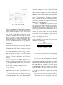
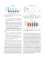
Towards Hardware Support for Common Sensor Processing Tasks
Adwait Gupte
Phillip Jones
Department of Electrical & Computer Engineering
Iowa State University
Ames, USA
[email protected]
Department of Electrical & Computer Engineering
Iowa State University
Ames, USA
[email protected]
Abstract—Sensor processing is a common task within
many embedded system domains, such as in control systems
sensor feedback used for actuator control, etc. In this paper
we have surveyed several embedded system domains, and
extracted kernels of computation that are common across applications within a given domain, or across domains. We have
shown that adding architectural support for executing these
common kernels of computation can yield an overall better
system performance. We present a light weight, simplified
prototype of a Sensor Processing Unit (SPU) that offloads
these computations from the main Arithmetic Logic Unit
(ALU) of an embedded processor, and that accesses sensor
data in a low latency manner. Our SPU prototype shows an
average speed up factor of 2.48 over executing these kernels
on an embedded PowerPC processor. A large portion of this
speed up is due to our low latency method for accessing sensor
data. Isolating our speed up to purely computation still shows
an average speed up factor of 1.38 for these kernels.
Index Terms—component; formatting; style; styling;
I.. I NTRODUCTION
The severe constraints placed on embedded systems in
terms of power consumption, memory availability and processing capability, and the ever increasing computational
demands placed on these systems make it crucial embedded processors are designed to efficiently perform the
tasks required of them. A majority of embedded systems
involve interaction with the physical world through some
kind of sensing mechanisms. However, based on our survey
of a wide range of microprocessors/microcontrollers that
have been conveniently organized by researches such as
Bokareva [1], it is clear there are no specific resources
available on these devices for efficiently processing sensor
data. Given this is such a common task, exploring how
the addition of sensor processing resources can improve
system efficiency appears to be a path worth pursuing, and
is the focus of this paper.
Figure 1 gives a high level summary of the contributions
of this paper. There are three specific areas of contribution.
First, a number of common computational kernels for
sensor processing have been identified. This helps justify
the allocation of hardware resources for the processing
of sensor data. Second, we have proposed a specialized
functional unit call the sensor processing unit (SPU) to
efficiently assist in the execution of these computations.
In addition, we have noted that the autonomous nature
of our approach lends itself to potentially act as a base
for creating an intelligent power management scheme.
Third, we have integrated a simplified prototype of our
functional unit with an embedded processor and evaluated
its performance on an FPGA-based platform.
II.. R ELATED W ORK
This section reviews three areas of related work. First,
embedded system benchmarks are discussed. Research in
this area is used as the starting point for our work. Then
the current state of the art in embedded processors, and
their relevant features are discussed in order to place our
work in perspective.
A. Embedded Benchmarks
The industry standard Embedded Microprocessor
Benchmark Consortium (EEMBC) benchmarks [2] aims
to standardize a set of common benchmarks for different
embedded system domains. These benchmarks are based
on common processing tasks that are found in each respective domain (e.g. Controls, Automotive, Communications).
Having a set of such benchmarks is useful for evaluating
a processor’s suitability for a given application, and for
characterizing the strengths and weaknesses of different
processors. MiBench [3] is another benchmark that targets
embedded systems. MiBench was developed in the same
spirit as EEMBC, but unlike EEMBC it is freely available
to academia.
These benchmarks provide a nice organization of the
processing tasks found in embedded systems. However,
neither the MiBench or the EEMBC benchmarks clearly
isolate kernels of computation associated with sensor processing. The EEMBC benchmarks does have a suite of
tests that focus on signal processing type tasks for which
digit signal processors (DSPs) are likely most appropriate.
Our work aims to extract simpler and more common sensor
processing kernels. It is envisioned that these kernels can
act as a starting point for developing a more extensive
sensor processing test suite in the future.
B. Embedded Processors
Bokareva surveys a number of sensor network nodes
(also know as motes), and processors that are used within
Fig. 1. 1) illustrates some high-level sensor dependent tasks identified within various embedded domains, 2) highlights common kernels
of computation that were identified, 3) shows conceptually how our sensor processing unit (SPU) integrates into an embedded system.
those nodes [1]. These processors range from simple 8-bit
microcontrollers (e.g. Atmel Atmega 128) to 32-bit microprocessors (e.g. Intel XScale processor family). However,
from an examination of a representative set of processor
Datasheets [4] [5] [6] [7], none of these processor were
found to have any special functionality to support sensor
processing tasks. The closest feature found was on the
Intel XScale processor family, an external interface for
a DSP coprocessor. Our work puts forth a lightweight
architectural extension for processing common sensor data
computations for which using a full blown DSP would be
an overkill.
Two features related to our work that are currently
found in either sensor network nodes and/or current high
performance processors are 1) waking up on the occurrence of an event, and 2) raising an exception when the
processor has surpassed a given temperature threshold.
Many processors/microcontrollers [8] [4] [5] [6], some of
which are currently used in sensor network nodes, have
the ability to go into a low power operating mode until an
interrupt indicates they should wake up. The Intel Centrino
chips also have the ability to come out of hibernation on
receiving data on their network interface (e.g. wake on
LAN technology [9]). Current chipsets such as the Intel
System Controller Hub can wake the main processor up
when a peripheral sends an event [10]. With respect to
thermal events, some microprocessors, such as the Intel
Atom Processor [11], have the ability to monitor their onchip temperature and response if this temperature surpasses
a given threshold (e.g. shutdown or transition into a lower
performance mode). The architecture of our light weight
SPU naturally allows interrupts to be used to notify the
main processor when simple to fairly complex combinations of sensors values are detected. This capability and its
potential implications are discussed further in Section IV
while some common kernels of computatio identified by
us are described in Section III.
III.. C OMMON K ERNELS OF C OMPUTATION
Due to the large and diverse set of domains in which
embedded systems are used, past works [2] [3] have tried
to identify common computational kernels that are used
across domains by abstracting away the specifics of individual applications. Similarly, we have tried to boil down
the diverse set of sensor processing tasks to a small set of
core kernels that are generic enough to find application in
many fields, and common enough to warrant the allocation
of processor chip real estate.
While many applications require massive processing of
sensor data using digital signal processing type algorithms,
there is a large base of applications [12] [13] [14] [15] that
consist of simpler processing tasks, and do not warrant the
overhead of having a full blown DSP. We have identified
and extracted five such tasks from the MiBench benchmark
and various other sources: Linear Equations, Moving Average, Average, Delta Value, and Threshold/Range Check.
Linear Equations: One of the simplest tasks that can
be performed on sensor data is the execution of a linear
mathematical operation on a single value or multiple values. In the automotive domain converting between radians
and degrees is identified as a common task in [3].
In the controls system domain the Proportional-IntegralDerivative (PID) controller is one of the most common
control algorithms used [16]. [17] and [14] give examples
of advanced PID controllers that can be boiled down to
calculating a set of linear equations involving sensor values
along with other computational functions.
Moving Average: Sometimes, sensors can be prone to
spurious spikes in their output. The moving average is
one method for reducing the effects of random “noise”
on sensor output. Over time measurements are averaged
together, and this average is used by the end application.
The impact of spikes in measurements are mitigated, while
actual changes in the physical quantity being measured are
eventually reflected by the average. The responsiveness of
the moving average can be tuned to reflect the known phys-
ical dynamics of the quantity being measured by added
appropriate weights to the previously computed average,
and the current sensor measurement (weighted moving
average). The moving average is a common method for
filtering sensor data [12] [18] [19] [20].
Average: Applications, such as sensor networks, often
measure physical quantities over a distributed area (e.g.
temperature). Averaging these distributed measurements is
a simple means for aggregating this information into a
compact form. This approach was used by Goebel [13],
Ganeriwal [21], and Nakamura [22]. In [12] Hellerstein
uses averaging as means of “cleaning” data obtained from
a group of sensors.
Delta Value: Often, the difference between the current
and previous value of the sensor (called delta) is used in
a lot of computation. eg: the “communication” suite of
benchmarks in [3] includes delta modulation, a process
of encoding which may be used to encode the output of
sensors before transmission. [15] presents another example
of using the “delta” value in a sensor based system.
Threshold/Range Check: There are various applications
in which the sensors values are required to be within
particular range or below/above a certain threshold for
the proper operation of the system. In such systems, some
sort of mechanism is needed to monitor the sensor values.
Alternatively, the systems might need to take some kind
of action when the sensor value breaches the defined
range/threshold bound.
This is by no means an exhaustive list of such kernels,
but having identified some common kernels of computation
across fields, in the next section we propose a unit, the
SPU, which could be a part of the architectures of future
embedded processors.
IV.. S ENSOR P ROCESSING U NIT (SPU) A RCHITECTURE
This section presents our lightweight mechanism for
sensor processing. First we provide and overview of the
SPU and some possible applications. Then we describe its
architecture. Finally we describe the development platform
and the prototype limitations.
A. Overview
The SPU is designed to be a functional unit within
an embedded processor. It has two main purposes 1)
to efficiently offload the execution of common sensor
processing tasks from the main ALU, and 2) to detect
events that are a function of sensor values. Here we discuss
the two major uses of the SPU, and how it could potentially
be used for power management.
Sensor Processing Offload: The SPU has been designed
to operate in the following manner. First a user application
programs the SPU with functions that need to be performed
on the output of one or more sensors. Once programmed
the SPU computes these functions continuously as sensors
data flows into the SPU. The output of the sensors are
directly connected to the SPU, thus the SPU reevaluates
its programmed functions autonomously of the rest of the
processor. When the user application requires the result of
one of the programmed function, it simply issues a single
instruction to fetch this value from a special register. This
is opposed to the traditional approach of 1) reading all
sensor values required by a function, and 2) computing the
function in software. In addition to increasing the speed at
which a given sensor processing function can be computed,
discussed in Section V, the SPU allows the rest of the
processor to focus on other tasks.
Event Detection: Each function programmed into the
SPU can have an event associated with it. An event checks
if the result of a given function is <,>,or = to a fixed
value, or if the result of a function is within or outside
a given range. It the associated condition is true then an
interrupt is sent to the main processor. The purpose of this
functionality is to allow the processor to work on other
tasks until a given event fires off, as opposes to having to
continuously poll sensor values and compute this event
checks in software. This capability targets application
that need to take actions when sensor values surpass a
given threshold (e.g. thermal shutdown condition), or fall
outside a acceptable range (e.g. voltage supply stability).
As indicated in Section II, current processors do have the
ability to react to simple events such a thermal overload.
The SPU is a lightweight means to generalize the type of
events that a processor can detect and respond to.
Power Management: Again, as discussed in Section II,
many processors and microcontrollers support a low power
mode from which they can be woken up by an interrupt. Given the SPU’s ability to operate on sensor data
autonomously of the rest of the processor, the SPU could
potentially be used as a lightweight mechanism that allows
the rest of the processor to go into, or come out of a low
power state based on sensor data.
B. Architecture
In this section we discuss the architecture of the SPU,
which is made up of five major component: Sensor Data
Extractor, Configuration Storage, Processing Unit, Result
Storage, and Interrupt Generator. Figure 2 illustrates the
architectural layout of the SPU.
Sensor Data Extractor: This block is responsible for
connecting the SPU to available sensors. It continuously
streams sensor data to the SPU’s Processing Unit, and
Interrupt Generator.
Configuration Storage: This is where configuration
information sent by a user application is stored. This
information includes the set of sensors a given functions
operates on, the operations and constants that define a
function, and threshold and range values associated with
events that can generate interrupts to the main processor.
Fig. 2.
Architecture of the SPU
Processing Unit: This unit is responsible for all computations in the SPU. It is a simple Multiply-Accumulate
module that multiplies sensor values with their associated
weights (found in Configuration Storage). After a function
has been computed, its value is stored in the Result Storage
block, and the Processing Unit is reinitialized. Then the
configuration parameters, and sensor values for the next
function are loaded into the Processing Unit. This allows
the Processing Unit to be time shared among many functions. If each function is assumed to executed in a single
clock cycle, then this unit can scale to a large number of
functions before noticeable latency issues associated with
stale data arise.
Result Storage: This block is used to store the results
calculated by the Processing Unit. When an application
requests the result of a given function, the value is fetched
from this block. As the number of functions computed
by the Processing Unit increases the staleness of the data
stored in the Result Storage block increases. However,
given that the clock rate of a processor is typically much
higher than the rate of change of sensors, the relatively
small time lag should be acceptable for most applications,
even for a computing a significantly large number of
functions.
Interrupt Generator: The Interrupt Generator is responsible for detecting when a sensor value, or function
computed by the Processing Unit satisfies criteria specified
by a user application. If a criteria is met, then an “event”
is said to have taken place. On the occurrence of an event
this unit sends an interrupt to the main processor.
C. Implementation
Here we describe the developmental platform used to
implement the SPU and point out the limitations of the
simplified prototype.
1) Development Platform: The platform used for this
work is based on reconfigurable hardware technology
call Field Programmable Gate Arrays (FPGAs). FPGAs
are devices that consist of a sea of generic logic gates
that can be configured to realize any arbitrary hardware
logic function. In addition to this powerful capability,
advanced families of FPGAs have on-chip resources such
as PowerPC processor cores, high-performance multipliers,
SRAM based memory blocks, sophisticated programmable
clock managers, and analog to digital converters that allow
sensors to connect directly to the FPGA’s computation
fabric. Specifically, our platform is the ML507 evaluation
platform. It is manufactured by Xilinx Corporation [23].
The development board hosts one of the most advanced
FPGA devices called the Virtex-5.
2) Prototype: A simplified prototype, which was similar to the proposed method except for being non scalable,
was implemented in order to run the experiments for
evaluation. The main limitations of the prototype were 1)
the prototype included an adder and multiplier for each of
the sensors instead of having the Processing Unit timeshared, 2) the System Monitor was used for extracting
sensor data in some of the test cases, while others simply
used a dummy sensor which supplied a constant value, 3)
the prototype only supports a single user program function,
and 4) it only supports three sensors.
Table I gives the logic resources consumed by the SPU
prototype implemented on the Virtex-5. As can be seen,
the SPU is very lightweight.
TABLE I
R ESOURCE U TILIZATION ON V IRTEX 5
Resource
Slice Registers
Slice LUTs
Used
108(0.2%)
206(0.4%)
Available
44800
44800
V. E VALUATION
In this section we present our methodology along with
our observations and analysis.
A. Methodology
A prototype of the SPU was implemented on an Xilinx
Virtex 5 FPGA on a Xilinx ML507 evaluation board [23].
The embedded PowerPC 440 is used as the processor while
the SPU is implemented in the FPGA fabric. The SPU is
connected to the processor using the Fabric Coprocessor
Bus (FCB). Both the FCB and the processor are run
at 200 MHz. The FCB connection allows User Defined
Instructions (UDIs) to be used to read the sensor data. A
Processor Local Bus(PLB) [24] also connects the PowerPC
to a pseudo sensor. Evaluation experiments the following
three setup:
• PLB : The pseudo sensor was read over the PLB by
the processor. The PLB is a part of the CoreConnect
specification and hence is the way in which many
Fig. 3. Comparing the execution time of various common kernels
on all three experimental setups. As seen here, the SPU is
typically fastest for most kernels.
cores are interfaced with the embedded PowerPC. On
such an embedded chip, the sensor signals would
usually be available to the processor only over the
PLB.
• UDI : The fact that the FCB is faster than the PLB
contributes somewhat to the improved performance of
the propose architecture. However, to show that this
is not the sole reason for the improvement we have
included this additional case, where the data is read
over the faster FCB, but without the SPU.
• SPU : The SPU was implemented on the FPGA, and
connected over the FCB. The processor used UDIs to
program the SPU, as well as to read data from it.
The three setups were compared with respect to three
metrics:
• Execution Time The amount of time required to
complete a certain number of iterations of the control
loop.
• Code Density Size of the compiled programs.
• Response Latency Latency between an event occuring
and its response starting execution (used for the
interrupt generation feature of the SPU).
B. Observations and Analysis
In this section we present the results of experimentation on our prototype implementations described in section IV-C.
1) Execution Time: As can be seen from Figure 3, the
execution time for the SPU was the lowest for most of
the kernels. When a function is implemented in hardware
it is usually expected that it will be faster, hence this
result presents no surprise. Also the execution time of both
the PLB and UDI cases varies as the tasks become more
complex, and will also vary as the number of sensors that
are used is varied (see Figure 4). On the other hand, for
the SPU the execution time remains more or less constant
for functions directly supported by the SPU. For functions
not directly supported by the SPU, execution times do
increase with the complexity. However, the execution time
Fig. 4. Experiments to show the effect of increasing the number
of sensors on the execution time of the “Average” kernel. As
seen here, regardless of the number of sensors, the time taken
for reading the result from the SPU will remain constant.
Comparing the executable size for various common
kernels on all three experimental setups. As seen here, the SPU
case is the smallest in most cases.
Fig. 5.
of the SPU will remain constant as the number of sensors
increases. It should be noted that as the number of sensors
increases the result provided by the SPU will become more
and more stale. Also as the number of sensors supported
increases, the resources required also increases. Across all
cases, the average speedup obtained using the SPU was
2.48 fold faster then the PLB setup. Against the UDI setup,
the SPU showed an average speedup factor of 1.38. This
shows the speedups obtained over the PLB setup are not
just because of the SPU using the faster FCB interface.
2) Code Density: As seen in Figure 5, the SPU presents
a clear advantage over the PLB setup in terms of code
density. This is again expected since communicating over
the PLB would entail some extra instructions for the
arbitration of the PLB. The SPU cases remain almost the
same as the UDI cases in terms of code density. The SPU
being only slightly better. On average the programs that
use the SPU were 68.6% the size of programs that used
the PLB. The difference in code size between the SPU and
UDI cases were negligible. It should be noted that the size
of the programs using the SPU varies very little with the
number of sensors being used, while the size of both the
PLB and UDI setups will increase.
architecture for the SPU. The scalability could be not only
in terms of additional sensors but also support for more
than one equation at a time.
R EFERENCES
Comparing the response latency across setups. The PLB
and UDI setups use polling, and the SPU generates interrupts.
Although the SPU case has a large latency, it gives a higher
throughput from the processor.
Fig. 6.
Another interesting point that should be noted is that
there is very little difference in the code sizes between
the UDI and SPU setups. Thus, even if the SPU itself is
not implemented on a processor, simply including such
a single instruction method of sensor access also gives
improvements in code size.
3) Response Time: As is clearly seen in Figure 6,
the response time of the SPU is much higher than the
other two setups due to the overhead of performing a
context switch by the interrupt handler. However, we have
considered only the simplest of cases where in the PLB and
UDI setups continuously polls the sensor without doing
anything else. In situations where the response time is
tightly constrained, such tight polling may be the only
option, but in cases where the response time is allowed to
be larger, the SPU presents another option. With the SPU
option the processor can continue executing other code
while the sensor monitoring responsibility is relinquished
to the SPU. The rest of the processor could even be put
into a low power state, and woken up only when specific
conditions are met. In this context it might be worth
looking into ways to reduce the context switching overhead
in embedded microprocessors in order to allow for better
response times (e.g. as in [25]).
VI.. C ONCLUSION AND F UTURE W ORK
In this paper we have 1) described a set of common
sensor processing tasks, 2) proposed a sensor processing
architectural extension for executing these common task,
and 3) prototyped and evaluated the performance of this
extension. Our evaluations show an average speed up
of 2.48 fold in processing these kernels on our sensor
processing unit (SPU), as compared to executing these
kernels purely in software over a standard peripheral bus.
We still show an average speed up of 1.38 fold over
executing these kernels purely in software, and using
a low latency coprocessor interface. Considering many
applications might require a large number of sensors, a
next step in this work is to further explore a scalable
[1] T.
Bokareva,
“Mini
hardware
survey,”
http://www.cse.unsw.edu.au/
sensar/hardware/hardware survey.html.
[2] http://www.eembc.org.
[3] M. R. Guthaus, J. S. Ringenberg, D. Ernst, T. M. Austin, T. Mudge,
and R. B. Brown, “Mibench: A free, commercially representative
embedded benchmark suite,” in IEEE 4th Annual Workshop on
Workload Characterization, Austin, TX, Dec. 2001.
[4] MSP430x15x, MSP430x16x, MSP430x161x Mixed Signal Microcontroller Datasheet, Texas Instruments.
[5] Atmel AVR Datasheets, Atmel.
[6] Intel PXA27x Processor Family Datasheet, Intel.
[7] PPC440x5 CPU Core: User Manual, IBM.
[8] IBM,
“Powerpc
4xx
faqs,”
http://www01.ibm.com/chips/techlib/techlib.nsf/techdocs/130
10F4A79FC026C87256DFA004D30D0#20.
[9] Intel Centrino Mobile Technology, Wake on Wireless LAN Feature,
Intel Inc.
[10] Intel System Controller Hub, Intel Inc.
[11] Intel Atom Processor Z5XX Series Datasheet, Intel Inc.
[12] J. Hellerstein, W. Hong, S. Madden, and K. Stanek, “Beyond average: Towards sophisticated sensing with queries,” in Proceedings
of IPSN, 2003.
[13] K. Goebel and W. Yan, “Correcting sensor drift and intermittency
faults with data fusion and automated learning,” in IEEE Systems
Journal, vol. 2, no. 2, June 2008.
[14] M. Petrov, I. Ganchev, and A. Taneva, “Fuzzy pid control of
nonlinear plants,” in Proceedings of Intelligent Systems, 2002.
[15] Y. S. Suh, “Send-on-delta sensor data transmission with a linear
predictor,” in MDPI Sensors, 2007.
[16] A. Isaksson and T. Hagglund, “Editorial,” in IEE Proceedings of
Control Theory Applications, vol. 149, no. 1, Jan. 2002.
[17] K. S. Tang, K. F. Man, G. Chen, and S. Kwong, “An optimal fuzzy
pid controller,” in IEEE Transactions on Industrial Electronics,
vol. 48, no. 4, Aug. 2001.
[18] S. R. Jeffery, G. Alonso, M. J. Franklin, W. Hong, and J. Widom,
“Declarative support for sensor data cleaning,” in Proceedings of
PerCom, 2006.
[19] L. Gu, D. Jia, P. Vicaire, T. Yan, L. Luo, A. Tirumala, Q. Cao, T. He,
J. A. Stankovic, T. Abdelzaher, and B. H. Krogh, “Lightweight
detection and classification for wireless sensor networks in realistic
environments,” in Proceedings of SenSys, San Diego, California,
2005.
[20] K. Liu, L. Chen, Y. Liu, and M. Li, “Robust and efficient aggregate
query processing in wireless sensor networks,” in Springer Science
+ Business Media, 2008.
[21] S. G. andC. Han, M. B., and Srivastava, “Going beyond nodal
aggregates: Spatial average of a continuous physical process in
sensor networks,” in Poster in Sensys, 2003.
[22] M. Nakamura, A. Sakurai, T. Watanab, J. Nakamura, and H. Ban,
“Improved collaborative environment control using mote-based
sensor/actuator networks,” in Proceedings of Conference on Local
Computer Networks, 2006.
[23] http://www.xilinx.com/products/devkits/HW-V5-ML507-UNI-G.htm,
Xilinx Corporation.
[24] CoreConnect
Documentation,
IBM
Corporation.
[Online].
Available:
http://www03.ibm.com/technology/power/licensing/coreconnect/index.html
[25] P. P. Xiangrong Zhou, “Rapid and low-cost context-switch through
embedded processor customization for real-time and control applications,” in Proceedings of Design Automation Conference, 2006.