1
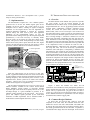
A real time electronics emulator with realistic data generation
for reception tests of the CMS ECAL front-end boards
T. Romanteau
Ph. Busson, C. Collard, A. Debraine, D. Decotigny, L. Dobrzynski, A. Karar, N. Regnault 1
Laboratoire Leprince Ringuet, 91128 Palaiseau, France
[email protected]
Abstract
The CMS [1] electromagnetic calorimeter (ECAL) [2]
uses 3 132 Front-End boards (FE) performing both trigger and
data readout functions. Prior to their integration at CERN, the
FE boards have to be validated by dedicated test bench
systems. The final one, called “XFEST” (eXtended Front-End
System Test) and for which the present developments have
been performed, is located at Laboratoire Leprince-Ringuet.
In this contribution, a solution is described to efficiently test a
large set of complex electronics boards characterized by a
large number of input ports and a high throughput data rate.
To perform it, an algorithm to simulate the Very Front End
signals has been emulated. The project firmwares use VHDL
embedded into XILINX Field Programmable Gate Array
circuits (FPGA). This contribution describes the solutions
developed in order to create a realistic digital input patterns
real-time emulator working at 40 MHz. The implementation
of a real time comparison of the FE output streams as well as
the test bench will be also presented.
I. INTRODUCTION
The present XFEST project is part of the electronics
boards validation system described in [3]. It has been
designed and built to test up to 12 FE boards at the same time.
The same digital input patterns, at a rate of 40 MHz, are sent
onto all Front End (FE) boards. Each FE receives an
equivalent of 25 channels 14 bits digital data streams at a 40
MHz clock frequency. The data are processed by dedicated
Asics called FENIX [4]. In order to emulate the 25 digital
input vectors, a prototype version of the FE board equipped
with commercial programmable circuits in place of the
FENIX Asics has been used. This board, called “EF”, is used
in a reverse mode to its original usage as FE prototype. One
EF is installed on a motherboard designed and developed at
LLR. The main role of this motherboard is to insure the
replication of the 25 digital signals in order to feed the FE
boards. In an initial phase of the project, it has been foreseen
to have three motherboards each one equipped with one EF in
order to test at the same time 12 FE boards. In the current
running, the system limits itself to one motherboard with four
FE (Figure 1).
1
Present address: LPNHE Paris VI-VII (http://www-lpnhep.in2p3.fr/)
Slow Control
FEC interface
LHC clock generation
25 data bus
Token Ring bus
Carte
EFCarte
EF EF
board
Carte
FECarte
FE FE
board
XFEST Test Platform
1 EF for stimuli + 4 EF in test
FE
board
FE
board
FE
board
Trigger path
TCC24
Optical Links
to TCC
Comparator
Test Bench Control
Data path
Parameter setting / Command
Figure 1: Display of the XFEST test bench
The outputs of the FE boards under test are shipped to a
prototype of the Trigger and Concentrator Card [5] (TCC24)
by optical fibres. The TCC24 is equipped with commercial
programmable circuits. In order to perform the real time
comparison of the FE outputs, the TCC24 has to run with a
dedicated firmware.
To achieve the validation goals two different firmwares
have been developed for the project as well as the interface to
drive the setup:
•
•
For the 25 signal emulators the following signal
characteristics have been implemented: the analogue
signal shape, its potential pileup, the electronics
noises and pedestals, the trigger occurrence
distribution and the signal amplitude which have
been randomly generated. Amplitude, gains, signal
range and level of noise are all adjustable via an
integrated I2 C interface [6]. This dedicated firmware
is loaded into the FPGA of the EF board.
For the comparison system, the main issue is to
aggregate and compare in a same clock domain all
data from different clock time buckets. The real time
computing of all input data is a key point to solve the
buffer control problems. The dedicated comparison
firmwares are loaded to the TCC24 FPGA’s.
• Parameters setup, like the reference card selection, is
possible through an embedded VME interface.
Diagnostic and access to error counting are included
in the design. The interface is described in [3].
The validation test for a set of FE, performed for about
one hour (equivalent to 1013 different patterns), is obtained
when all trigger and data outputs are identical during the
testing time at the bits level.
II. PATTERN GENERATION SOLUTION
A. Overview
Five Virtex2 FPGAs, from XILINX, present on the EF
board are reprogrammed in a reverse mode to emulate the
signals send by the VFE electronics. These FPGA devices,
called ‘PATGEN’, work with an embedded firmware
providing pattern generator data. A sixth FPGA device on the
EF board is used to control and synchronise all the others by a
start/stop software command. An I2 C interface is used for the
internal parameters setting.
To test more efficiently the discrimination capabilities of
the FE board, it has been decided to favour a signal amplitude
distribution with low level amplitudes rather than the high
one.
(7.6 hours) is low by using a high bit length number. The
possibility to work within a pre-defined range of energy can
also be set by defining minimum and maximum amplitude
values accessible through internal registers. To achieve it, a
new IEEE VHDL package [7] has been experimented.
The digitally coded waveform of the signal is stored in a
memory and can be modified by the user. Two memory
outputs can be mixed to produce a realistic pileup shape. The
automatic gain switching as well as the pedestal and the noise
of the ECAL VFE electronics MGPA 3 Asics chip can also be
emulated4 . This specific implementation is now in operation.
All parameters of the ‘PATGEN’ devices can be set by
the user via the embedded I2 C interface. The user can also
access and control the registers providing the test status. The
interface is controlled by a software application described in
[3].
Figure 3 shows the block diagram of a single channel
pattern generator. A pipelined architecture has been chosen to
guaranty that it will run at the LHC clock frequency.
Figure 3: Block diagram and resources of a single channel Pattern
Generator device (PATGEN)
B. Simulation phase
Figure 2: Shape of the signal amplitude distribution (top) provided
by the EF pattern generator. It is obtained by mixing (middle) several
non-correlated LFSR (low) distribution.
A single side triangle distribution, as shown of Figure 2 (top
histogram) is used for the signal model. The algorithm also
allows event pileup at a level of 10%. To obtain the signal
distribution, a uniform pseudo random number generator2 has
been synthesized in the FPGAs providing a flat distribution as
shown on Figure 2 (bottom histogram). By mixing several
non-correlated LSFR, one obtains a triangle distribution as
shown on Figure 2 (middle histogram). The noise is also
emulated with another LFSR whose repeatability sequence
2
Based on a Logical Shift Feedback Register (LFSR). Initialisation with a
seed equal for which all bits are at ‘1’ or ’0’ is forebidden.
To check by simulation the signal amplitude distribution,
two methodologies have been developed. The first one uses
Matlab/Simulink software, and is a very fast methodology,
but the connection with the HDL model did not exist when
our tests have been carried out. The second one uses a library
of specific procedures developed in VHDL. It has been
implemented in the test bench at the top level. The standard
HDL simulator console then exhibits a pseudo graphic
distribution curve. Several data files including the values
produced with the HDL simulation have been produced and
successfully imported within the ROOT [8] framework for
analysis.
Another important point has been to check the access to
the internal registers. They are used to implement the
stop/start commands and study the effect of the parameters
change. Thanks to the re-use of an I2 C IP and the CERN
simulation library, it has been possible to carry out these tests
easily. Performing these tests in a HDL simulation
3
Multiple Grain Pre-Amplifier Electromagnetic Calorimeter readout chip for
CMS
4
For each of the three available gains the user has a set of internal registers to
define the value of gain, pedestal and noise.
III. TRIGGER AND DATA PATH ANALYSIS
environment allowed a fast development and a precise
analysis on the generated data.
A. Overview
Figure 4: General and detailed implementation views of the
“PATGEN“ FPGA. All kind of available resources are used.
Since the whole design can be viewed as a data path
system, a pipelined architecture has been used. The insertion
of some pipeline registers along the path allowed reaching the
working frequency. The total latency does not have a real
importance here, but the system has to work at the nominal
frequency. However this type of architecture increases the
number of used registers in a significant way.
The developed architecture gives access to a large set of
internal resources available in the Virtex2 device (Block
RAM, multiplier, tri-state buffer). It represents 860.000
equivalent gate count and a die occupancy ratio of 70 %. The
developed design is a good candidate to perform, as an
efficient testing platform of the FE boards. This project
proves that complex signals provided by the Front End
electronics of HEP experiments can be emulated within a
dedicated and versatile digital electronics system.
5
Intellectual Proprietary electronic block, based on an assembly of logical
primitives and provided by an outside source
TCC24
1x I 2 C Interface
TCCvi
5 x Pattern generators
The main function of the XFEST test system is to provide
the same signals to the FE boards plugged on the
motherboard. Each of them sends, via two optical links, their
output information to a TCC24 [5] prototype board. One link
(Trigger Path) continuously transmits computed trigger
vectors, the second one (Data Path) sends the internal
buffered data, when a L1A event accept is sent to the FE via
the Token Ring (Daisy chain bus used for inter-connexion of
the FE board). The emulated signals are built out of 25 data
buses arriving through 5 connectors soldered on each FE
board. Each FE board synchronizes the data with the LHC
clock distributed via the Token Ring port and delivered by a
FEC [9] board. Due to the time delay between two FE boards,
this clock is provided to each board with a time lag which has
to be compensated. This is achieved for each FE with a
dedicated hardware, called PLL [10]. All boards, respecting
the setup data time, can not be necessarily synchronized
within the same clock phase. Consequently, a different clock
time domain is also created for each of them. The data buffer
made out of headers, control words and real data is sent to the
associated deserialisers of the TCC24. On the reception side,
each of them will be retrieved from the serial data stream by a
deserialiser component. The outputs of these components are
connected to FPGA programmable devices. On their own
path, the named functions ‘TRIGPATH’ and ‘DATAPATH’,
embedded in these programmable devices will check that all
received data for all channels are the same.
TCCex
All functionalities required for a five channels pattern
generator have to fit the one million logical gates device
available on the EF board. The system needs up to 41
multipliers and 53 adders, working in signed or unsigned
arithmetic. As the targeted device does not embedded all
requested dedicated multipliers a XLINX IP5 generator
software library has been used to place some pipelined
multipliers on the programmable matrix. To ease the
placement and the routing, and respect the temporal requested
performances, it has been necessary to manually define
physical sectors on the matrix for each large subset of the
design. This process called "floor-planning" can also clearly
reduce the necessary time to place and route the cells. Figure
4 shows the affected physical areas for each of the 5 pattern
generators sub blocs and for an I2 C interface functions.
S BS Controle r
C. Implementation
VME Crate
PC Driven
CH1
JTAG bus
25data bus
12 Optical encapsulated Fibber
Token Ring bus / LHC clock transport
Optical fibber link
AGILENT 81134 A
Pulse /Pattern Generator
-
+
EF
board
CH 2
-
+
XFEST Test Platform
Trigger path
XFESTclicforstart
Fhxshgfdhh
1 2 3 3 4 4 4 rrtttyuu
Gfhfhf hg kj mh
1 2 2 7 7 7 ttrguii
Optical Links
to TCC24
1 EF for stimuli + 4 EF in test
4 5 5 6
8
.7
4 5 5 7
Test Bench Control
FEC card inside
ChipScope
Console
FE
board
FE
board
FE
board
FE
board
Data path
Figure 5: XFEST test bench in 4 boards’ configuration
Figure 5 shows the XFEST test bench and all
connections. An AGILENT 81134A pulse/pattern generator is
used to emulate the LHC clock. It is connected to a couple of
boards: TTCvi [11] and TTCex [11] part of the TTC LHC’s
system [11], and to the TCC24 prototype board. Its FPGA’s
receive dedicated firmware to perform the real time analysis
for both the Data and the Trigger paths.
B. Common Design Solutions
To insure that all received data could be read and
compared at the same time; the extracted clocks for each
channel are used to write into a FIFO buffer. All buffers will
be read by the same clock source not phased with any others,
but locally generated inside the TCC24 board. To perform it,
a dedicated FIFO design has been developed. In the Virtex2
architecture a block RAM can be used and concurrently
accessed from both sides if and only if the read address and
the write address are not the same. To solve this problem,
both data and address information are stored in a single
memory location. Moreover a feedback mechanism is used.
With this method the FIFO is self-addressing so no external
counters are required. A number of ‘n’ address bits are fed
back from the RAM output data port to its address port. The
same ‘n’ bits are also fed to a simple incremental circuit. The
output of the incremental circuit is combined with the
incoming data word. This address plus the data word are then
written synchronously into the next memory location. The
clock load for the incoming part is one, thus it is not necessary
to use the available global clock tree and their dedicated
buffer limited in the Virtex2 family. Up to 12 incoming clock
domains plus a local one have been taken into account. The
final goal is to collect data in all clock domains and access
them in a single one. This solution is well adapted to the
needs and works fine.
To avoid working on the data buffer when entries are
received a solution based on the comparison of the received
data in real time has been adopted. A channel must be defined
as the reference for the comparison. The user is able to define
it through an internal register accessible through the VME
interface. The comparison errors, the transmission errors or
the loss of synchronization of the serial links are counted and
written into registers accessible through the VME interface.
Figure 6: ChipScope-Pro windows with “TRIGPATH“ (on the front)
displaying an error on channel 3 and “DATAPATH“ waveform
(behind)
The channel synchronization loss debugging has been a
real issue. A specific solution based on the use of ‘ChipScopePro’ software [13] from XILINX, has been adopted. This
software application can be seen as an internal logic analyzer
that exhibits all stored signals values when a predefined event
value occurs. The signals to display are selected by the user.
Internal RAM blocks are used as acquisition memories and
clocked inside the TCC24 with the local LHC clock. Figure 6
shows a snap shot of this application. A synchronisation loss
can be seen on channel 3. This application has been really
useful to investigate the data returned through the VME
interface when an error happens. To perform the comparison,
all channels have to be synchronised on the same data. It is
then necessary to correctly adjust the PLL values on all FE
boards in test, as depicted before. This is achievable if the
cumulated delay time between several FE boards does not
exceed one clock cycle. For more than 4 boards this request is
no more satisfied, consequently a specific hardware has to be
implemented in the ‘DATAPATH’ and the ‘TRIGPATH’
FPGA’s firmwares. Then, it has been foreseen, for the
comparison alignment and for each channel the ability to
automatically introduce a programmable delay to adjust the
phase of the different signals with the reference one (up to 3
clock cycles). An effective comparison starts when all
channels have adjusted their necessary latency and return a
‘Phase OK’ information flag. A scalable design has been
created by using VHDL generic parameters. With them, it is
easy to adapt the hardware designs to the number of FE board
on the test bench.
C. Specific solution for the DATAPATH
The main specificity of the ‘DATAPATH’ concerns the
data storage sent in a burst mode when a L1A event occurs. A
well-defined data block format [4] is then transferred to the
TCC24. Each FE board handles 25 crystals data, named
Trigger Tower (TT). It concerns 5 Strips of 5 Channels each.
The format includes a TT header, a Strip header and a
Channel header. Moreover, each channel header includes the
data frame length. This length can be dynamically set to zero
by the FE board, to prevent the data overflow when too many
L1A appear in a short period of time. In this case the header,
the bunch crossing identifier information (BCID), the event
identifier (EVID) and the computed checksum are only
present into the DAQ data block format. The performed
comparison electronics must have the capability to detect and
extract from the internal headers and identifiers the presence
of data. A variable frame length has then to be supported
corresponding to various block sizes produced by the FE
boards. To manage this, a real time finite state machine has
been implemented for each channel.
The percentage of data with empty blocks is automatically
computed during the comparison process and written to a
register for each channel under test. These results can be
accessed by the VME interface.
IV. CONCLUSIONS
During the development of this project, it has been
checked, that original hardware solutions could be developed
for very challenging tasks. Real time emulation of existing
electronics boards has been a key start point for the test
bench. They are required to validate electronics boards which
have to be integrated in the detector without any possibility of
maintenance like for the space projects.
The validation of several thousands of electronics boards
for the CMS electromagnetic calorimeter requires a robust test
bench system. A limited design time has forced us to reduce
risk by reusing existing prototype electronics board made with
re-programmable devices. The use of VHDL to produce
FPGA firmwares allows flexible hardware solutions and
realistic conditions of test. A deep interaction between the
software and the hardware has been successfully achieved.
V. REFERENCES
[1] CMS Collaboration: “The Compact Muon Solenoid”.
Technical Proposal”, CERN/LHCC 94-38
[2] CMS Collaboration : “ECAL Technical Design
Report”, CERN/LHCC 97-33, CMS TDR 4, 15
December 1997
[3] C. Collard et al., “CMS ECAL Front-End boards: the
XFEST project.” contribution paper to the current
conference.
[4] FENIX ASIC version 1.0, HDL description version 8f
Specification, Mars 2003, CERN, by Magnus Hansen
[5] Pascal Paganini et al., “TCC24 reference to Tests of
the boards generating the CMS ECAL Trigger
Primitives: from the On-Detector electronics to the
Off-Detector electronics system”. Proceedings of
LECC2004 Boston, from 13-17 September 2004
[6] Inter-IC bus from PHILIPS. It is a serial control bus
that provides in a system, the communications link
between integrated circuits
[7] Fixed point VHDL packages by David Bishop, see at
address:
http://www.eda.org/vhdl-200x/vhdl-200xft/packages/files.html
[8] ROOT, an object oriented data analysis framework
for physic experiment: http://root.cern.ch/
[9] Front End Controller, an interface board that hosts
token rings for the communication with the Control
and Communication Unit (CCU) modules, see also
[12].
[10] QPLL User Manual, v1.1, January 2005, CERN
Microelectronics Group. More information at WEB
address: http://proj-qpll.web.cern.ch/proj-qpll/
[11] Timing, Trigger and Control (TTC) Systems for the
LHC, initially developed by RD12 for CERN. More
information
at
WEB
address:
http://ttc.web.cern.ch/TTC/intro.html
[12] F. Drouhin & al, “The CERN CMS Silicon Strip
Tracker Control System”. CMS CR 2004/032, August
2004, CERN
[13] ChipScope-Pro, real time debug and verification tool
from XILINX:
http://www.xilinx.com/ise/optional_prod/cspro.htm