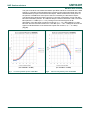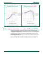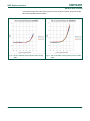
1
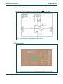
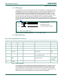
UM10497 User manual for the BGU8007 GPS LNA evaluation board Rev. 1.0 — 5 October 2011 User manual Document information Info Content Keywords LNA, GPS, BGU8007 Abstract This document explains the BGU8007 GPS low noise amplifier evaluation board UM10497 NXP Semiconductors BGU8007 GPS LNA EVB Revision history Rev Date Description 1.0 20111005 First Release. Contact information For additional information, please visit: http://www.nxp.com For sales office addresses, please send an email to: [email protected] UM10497 User manual All information provided in this document is subject to legal disclaimers. Rev. 1.0 — 5 October 2011 © NXP B.V. 2011. All rights reserved. 2 of 16 UM10497 NXP Semiconductors BGU8007 GPS LNA EVB 1. Introduction NXP Semiconductors’ BGU8007 is a low-noise amplifier for GPS receiver applications in a plastic, leadless 6 pin, extremely thin small outline SOT886 package. It has a current of [1] 4.6 mA, a gain of 19 dB and a noise figure of 0.75 dB . It has superior linearity performance to suppress interference and noise from co-habitation cellular transmitters while retaining sensitivity. The LNA has been designed using NXP Semiconductors’ advanced 180 GHz fT SiGe:C process. The BGU8007 only requires two external components, one series inductor for input matching and one decoupling capacitor. The BGU8007 contains one RF stage and internal bias that is temperature stabilized. It is also supplied with an enable function allowing it to be controlled by a logic signal. The BGU8007 is ideal for use as GNSS LNA in smart phones, feature phones and Portable Navigation Devices. The GPS LNA evaluation board (EVB), see Fig 1, is designed to evaluate the performance of the BGU8007 applied as a GPS LNA. In this document, the application diagram, board layout, bill of materials, and typical results are given, as well as some explanations on GPS related performance parameters like out-of-band input third-order intercept point, gain compression under jamming and noise under jamming. Fig 1. UM10497 User manual BGU8007 GPS LNA evaluation board All information provided in this document is subject to legal disclaimers. Rev. 1.0 — 5 October 2011 © NXP B.V. 2011. All rights reserved. 3 of 16 UM10497 NXP Semiconductors BGU8007 GPS LNA EVB 2. General description NXP Semiconductors’ BGU8007 low noise amplifier is dedicated for the GNSS frequency band (GPS, GLONASS and Galileo positioning systems). The integrated biasing circuit is temperature stabilized, which maintains a constant current over temperature. It also enables the superior linearity performance of the BGU8007. It is also supplied with an enable function that allows it to be controlled with a logic signal. In disabled mode it consumes less than 1 µA. The output of the BGU8007 is internally matched for 1575.42 MHz whereas only one series inductor at the input is needed to achieve the best RF performance. Both the input and output are AC coupled via an integrated capacitor. Only two external components are required to build a GPS LNA with the following advantages: Low noise; High gain; High linearity under jamming; Very low package height 0.5mm; Low current consumption; Short power settling time; The data sheet of the BGU8007 is available, and it is called “SiGe:C Low Noise Amplifier MMIC for GPS, GLONASS and Galileo” 3. Application Board The BGU8007 GPS LNA evaluation board simplifies the evaluation of the BGU8007 GPS LNA for the GNSS applications. The evaluation board enables testing of the device performance and requires no additional support circuitry. The board is fully assembled with the BGU8007, including the input series inductor as well as a decoupling capacitor to optimize the performance. The board is supplied with two SMA connectors for input and output connection to RF test equipment. The BGU8007 can operate from a 1.5 V to 2.2 V single supply and consumes about 4.6mA. UM10497 User manual All information provided in this document is subject to legal disclaimers. Rev. 1.0 — 5 October 2011 © NXP B.V. 2011. All rights reserved. 4 of 16 UM10497 NXP Semiconductors BGU8007 GPS LNA EVB 3.1 Application Circuit The circuit diagram of the evaluation board is shown in Fig 2. With jumper JU1 the enable pin can be controlled to either to Vcc or GND. Fig 2. Circuit diagram of the BGU8007 evaluation board 3.2 Board Layout Fig 3. UM10497 User manual Printed circuit board lay-out of the BGU8007 GPS LNA evaluation board All information provided in this document is subject to legal disclaimers. Rev. 1.0 — 5 October 2011 © NXP B.V. 2011. All rights reserved. 5 of 16 UM10497 NXP Semiconductors BGU8007 GPS LNA EVB 3.3 PCB layout A good PCB layout is an essential part of an RF circuit design. The evaluation board of the BGU8007 can serve as a guideline for laying out a board using the BGU8007. Use controlled impedance lines for all high frequency inputs and outputs. Bypass V cc with decoupling capacitors, preferably located as close as possible to the device. For long bias lines it may be necessary to add decoupling capacitors along the line further away from the device. Proper grounding of the GND pins is also essential for good RF performance. Either connect the GND pins directly to the ground plane or through vias, or do both. The material that has been used for the evaluation board is FR4 using the stack shown in Fig 4 20um Cu 0.2mm FR4 critical 20um Cu 0.8mm FR4 only for mechanical rigidity of PCB 20um Cu Fig 4. Stack of the PCB material Material supplier is ISOLA DURAVER; r = 4.6 - 4.9: Tan= 0.02 3.4 Bill of materials Table 1 BOM of the BGU8007 GPS LNA EVB v2.1 Designator Description Footprint Value Supplier Name/type Ac BGU8007 1.45x1.0mm PCB v2.1 35x20mm BGU8007 GPS LNA EVB C1 Capacitor 0402 1nF Murata GRM1555 Decoupling L1 Inductor 0402 5.6nH Murata/LQW15A High Q low Rs Input matching X1,X2 SMA RF connector - - Johnson, End launch SMA RF input/ RF output X3 DC header - - Molex, PCB header, Right Angle, 1 row, 3 way 90121-0763 X4 JUMPER stage - - Molex, PCB header, Vertical, 1 row, Connect Ven to 3 way 90120-0763 Vcc or separate Ven voltage JU1 Jumper Comment LNA MMIC 142-0701-841 Bias connector 3.4.1 Series inductor The evaluation board is supplied with Murata LQW15series inductor of 5.6nH. This is a wire wound type of inductor with high quality factor (Q) and low series resistance (R s). This type of inductor is recommended in order to achieve the best noise performance. High Q inductors from other suppliers can be used. If it is decided to use other low cost inductors with lower Q and higher Rs the noise performance will degrade. UM10497 User manual All information provided in this document is subject to legal disclaimers. Rev. 1.0 — 5 October 2011 © NXP B.V. 2011. All rights reserved. 6 of 16 UM10497 NXP Semiconductors BGU8007 GPS LNA EVB 4. Required Equipment In order to measure the evaluation board the following is necessary: DC Power Supply up to 30 mA at 1.5 V to 2.2 V; Two RF signal generators capable of generating an RF signal at the operating frequency of 1575.42 MHz, as well as the jammer frequencies 850 MHz, 1713.42 MHz, 1850 MHz and 1851.42 MHz; An RF spectrum analyzer that covers at least the operating frequency of 1575.42 MHz as well as a few of the harmonics, so up to 6 GHz should be sufficient; “Optional” a version with the capability of measuring noise figure is convenient; Amp meter to measure the supply current (optional); A network analyzer for measuring gain, return loss and reverse Isolation; Noise figure analyzer and 5 dB noise source like the Agilent 346A is recommended; Directional coupler; Proper RF cables. 5. Connections and setup The BGU8007 GPS LNA evaluation board is fully assembled and tested. Please follow the steps below for a step-by-step guide to operate the evaluation board and testing the device functions. 1. Measure the cable- and directional coupler losses at the frequencies which are used during the evaluation (1575 MHz, 850 MHz and 1850 MHz). These losses are used to correct the measured power levels. 2. Connect the DC power supply to the Vcc, and GND terminals. Set the power supply to the desired supply voltage, between 1.5 V and 2.2 V, but never exceed 2.5 V as it might damage the BGU8007. 3. Jumper JU1 is connected between the Vcc terminal of the evaluation board and the Ven pin of the BGU8007. Fig 5 shows the evaluation board including its connections. 4. To evaluate the power on settling time ton and the power off settling time toff, it is also possible to use a separate voltage on the Ven, eventually this voltage can be supplied by a pulse generator. In this case jumper JU1 should be removed. The definition of ton is the time from 10 % to 90 % of the maximum signal level and for toff the time from 90 % to 10 % of the maximum signal level. 5. Connect the RF signal generator and the spectrum analyzer to the RF input and the RF output of the evaluation board, respectively. Do not turn on the RF output of the Signal generator yet, set it to -40 dBm output power at 1575.42 MHz, set the spectrum analyzer at 1575.42 MHz center frequency and a reference level of 0 dBm. 6. Turn on the DC power supply and it should read approximately 4.6mA. 7. Enable the RF output of the generator; the spectrum analyzer displays a tone of around –25 dBm at 1575.42 MHz.Instead of using a signal generator and spectrum analyzer one can also use a network analyzer in order to measure gain as well as inand output return loss. 8. For noise figure evaluation, either a noise-figure analyzer or a spectrum analyzer with noise option can be used. When measuring the noise figure of the evaluation board, any kind of adaptors, cables etc between the noise source and the evaluation board should be avoided, since this affects the noise performance. UM10497 User manual All information provided in this document is subject to legal disclaimers. Rev. 1.0 — 5 October 2011 © NXP B.V. 2011. All rights reserved. 7 of 16 UM10497 NXP Semiconductors BGU8007 GPS LNA EVB 9. For noise under jamming conditions, the following is needed. A 5dB ENR noise source, a directional coupler, GPS band pass filter, a noise-figure analyzer or a spectrum analyzer with noise option can be used. See Fig 11 Fig 5. UM10497 User manual GPS LNA evaluation board including its connections All information provided in this document is subject to legal disclaimers. Rev. 1.0 — 5 October 2011 © NXP B.V. 2011. All rights reserved. 8 of 16 UM10497 NXP Semiconductors BGU8007 GPS LNA EVB 6. Linearity At the average power levels of –130 dBm that have to be received by a GPS receiver, the system will not have in-band intermodulation problems caused by the GPS-signal itself. Strong out-of-band cell phone TX jammers however can cause linearity problems, and result in third-order intermodulation products in the GPS frequency band. In this chapter the effects of these Jammer-signals on the Noise and Gain performance of the BGU8007 are described. The effect of these Jammers on the In-band and Out-of-Band Third-Order Intercept points are described in more detail in a separate User Manual: UM10453: 2-Tone Test BGU7005 and BGU7007 GPS LNA. 6.1 1 dB gain compression at 1575 MHz with 850 MHz or 1850 MHz jammers As already stated before, signal levels in the GPS frequency band of –130 dBm average will not cause linearity problems in the GPS band itself. This of course is also valid for the 1 dB gain compression in-band. The 1 dB compression point at 1575 MHz caused by cell phone TX jammers however is important. Measurements have been carried out using the set-up shown in Fig 6. The jammer signal is coupled via a directional coupler to the DUT. For the P1dB measurements this not required, but connecting it this way the setup can also be used for NF-measurements as described in the next paragraph. Fig 6. Noise under jamming measurement setup UM10497 User manual All information provided in this document is subject to legal disclaimers. Rev. 1.0 — 5 October 2011 © NXP B.V. 2011. All rights reserved. 9 of 16 UM10497 NXP Semiconductors BGU8007 GPS LNA EVB The gain of the DUT was measured between port RFin and RFout of the EVB at the GPS frequency 1575 MHz, while simultaneously a jammer power signal was swept at the 20 dB attenuated input port of the Directional Coupler. Please note that the drive power of the jammer is 20 dB lower at the input of the DUT caused by the directional coupler. The figures below show the supply-current (Icc) and gain compression curves with 850 MHz and 1850 MHz jammers. At 1 dB Gain drop the Jammer-Generator read out for 850 MHz jammer is +7 dBm (Vcc = 1.8 V). Taking into account the approx 20 dB attenuation of the directional coupler this means Pi(1dB) = –12.1 dBm (Fig 8). For 1850 MHz the Jammer-Generator read out is +10.9 dBm (Vcc = 1.8 V. Taking into account the approx 20 dB attenuation of the directional coupler this means Pi(1dB) = – 9.4 dBm). (Fig 10). (Pin 1575 MHZ = -45 dBm) (Pin 1575 MHZ = -45 dBm) Fig 7. Icc versus jammer power at 850 MHz UM10497 User manual Fig 8. Gain versus jammer power at 850 MHz All information provided in this document is subject to legal disclaimers. Rev. 1.0 — 5 October 2011 © NXP B.V. 2011. All rights reserved. 10 of 16 UM10497 NXP Semiconductors BGU8007 GPS LNA EVB (Pin 1575 MHZ = -45 dBm) Fig 9. (Pin 1575 MHZ = -45 dBm) Icc versus jammer power at 1850 MHz Fig 10. Gain versus jammer power at 1850 MHz 7. Noise figure as function of jammer power at 850 MHz and 1850 MHz Noise figure under jamming conditions is a measure of how the LNA behaves when e.g. a GSM TX interfering signal is at the input of the GPS antenna. To measure this behavior the setup shown in Fig 11 is used. The jammer signal is coupled via a directional coupler to the DUT: this is to avoid the jammer signal damaging the noise source. The GPS BPF is needed to avoid driving the second-stage LNA in saturation. For the Jammer-Generator a low Phase-Noise type is advised. This is to avoid extra noise caused by the Jammer-Generator at measurement frequency (1575 MHz). UM10497 User manual All information provided in this document is subject to legal disclaimers. Rev. 1.0 — 5 October 2011 © NXP B.V. 2011. All rights reserved. 11 of 16 UM10497 NXP Semiconductors BGU8007 GPS LNA EVB Fig 11. Noise under jamming measurement setup UM10497 User manual All information provided in this document is subject to legal disclaimers. Rev. 1.0 — 5 October 2011 © NXP B.V. 2011. All rights reserved. 12 of 16 UM10497 NXP Semiconductors BGU8007 GPS LNA EVB In the figures below the noise figure (NF) as function of jammer power are given for 850 MHz and 1850 MHz jammer signals. Fig 12. NF at 1.575 GHz versus jammer power at 850 MHz UM10497 User manual Fig 13. NF at 1.575 GHz versus jammer power at 1850 MHz All information provided in this document is subject to legal disclaimers. Rev. 1.0 — 5 October 2011 © NXP B.V. 2011. All rights reserved. 13 of 16 UM10497 NXP Semiconductors BGU8007 GPS LNA EVB 8. Typical Evaluation Board results Table 2, typical results measured on the Evaluation Boards. Operating Frequency is f=1575.42 MHz unless otherwise specified; Temp = 25 C. Parameter Symbol Supply Voltage Vcc 1.5 1.8 2.2 V Supply Current Icc 4.5 4.6 5.0 mA Noise Figure NF 0.75 0.75 0.75 dB Pin < -40 dBm, no jammer Power Gain Gp 19 19 19 dB Pin < -40 dBm, no jammer Input Return Loss RLin 5.5 5.5 5.5 dB Pin < -40 dBm, no jammer Output Return Loss RLout 26 26 26 dB Pin < -40 dBm, no jammer Reverse Isolation ISLrev 24 24 24 dB Pin < -40 dBm, no jammer Input 1dB Gain Compression Pi(1dB) -12 -11 -10 dBm 1559 MHz to 1610MHz Compression Input third order intercept point IP3i 4 4 5 dBm [1] [2] BGU8007 Unit [1] The losses of the connectors and the PCB of approximately 0.05dB are subtracted. [2] Jammers at f1 = f+138 MHz and f2 = f+276 MHz, where f = 1575.42 MHz. UM10497 User manual All information provided in this document is subject to legal disclaimers. Rev. 1.0 — 5 October 2011 Remarks © NXP B.V. 2011. All rights reserved. 14 of 16 UM10497 NXP Semiconductors BGU8007 GPS LNA EVB 9. Legal information 9.1 Definitions Draft — The document is a draft version only. The content is still under internal review and subject to formal approval, which may result in modifications or additions. NXP Semiconductors does not give any representations or warranties as to the accuracy or completeness of information included herein and shall have no liability for the consequences of use of such information. 9.2 Disclaimers Limited warranty and liability — Information in this document is believed to be accurate and reliable. However, NXP Semiconductors does not give any representations or warranties, expressed or implied, as to the accuracy or completeness of such information and shall have no liability for the consequences of use of such information. In no event shall NXP Semiconductors be liable for any indirect, incidental, punitive, special or consequential damages (including - without limitation lost profits, lost savings, business interruption, costs related to the removal or replacement of any products or rework charges) whether or not such damages are based on tort (including negligence), warranty, breach of contract or any other legal theory. Notwithstanding any damages that customer might incur for any reason whatsoever, NXP Semiconductors’ aggregate and cumulative liability towards customer for the products described herein shall be limited in accordance with the Terms and conditions of commercial sale of NXP Semiconductors. Right to make changes — NXP Semiconductors reserves the right to make changes to information published in this document, including without limitation specifications and product descriptions, at any time and without notice. This document supersedes and replaces all information supplied prior to the publication hereof. Suitability for use — NXP Semiconductors products are not designed, authorized or warranted to be suitable for use in life support, life-critical or safety-critical systems or equipment, nor in applications where failure or malfunction of an NXP Semiconductors product can reasonably be expected to result in personal injury, death or severe property or environmental damage. NXP Semiconductors accepts no liability for inclusion and/or use of NXP Semiconductors products in such equipment or applications and therefore such inclusion and/or use is at the customer’s own risk. Applications — Applications that are described herein for any of these products are for illustrative purposes only. NXP Semiconductors makes no representation or warranty that such applications will be suitable for the specified use without further testing or modification. Customers are responsible for the design and operation of their applications and products using NXP Semiconductors products, and NXP Semiconductors accepts no liability for any assistance with applications or UM10497 User manual customer product design. It is customer’s sole responsibility to determine whether the NXP Semiconductors product is suitable and fit for the customer’s applications and products planned, as well as for the planned application and use of customer’s third party customer(s). Customers should provide appropriate design and operating safeguards to minimize the risks associated with their applications and products. NXP Semiconductors does not accept any liability related to any default, damage, costs or problem which is based on any weakness or default in the customer’s applications or products, or the application or use by customer’s third party customer(s). Customer is responsible for doing all necessary testing for the customer’s applications and products using NXP Semiconductors products in order to avoid a default of the applications and the products or of the application or use by customer’s third party customer(s). NXP does not accept any liability in this respect. Export control — This document as well as the item(s) described herein may be subject to export control regulations. Export might require a prior authorization from competent authorities. Evaluation products — This product is provided on an “as is” and “with all faults” basis for evaluation purposes only. NXP Semiconductors, its affiliates and their suppliers expressly disclaim all warranties, whether express, implied or statutory, including but not limited to the implied warranties of noninfringement, merchantability and fitness for a particular purpose. The entire risk as to the quality, or arising out of the use or performance, of this product remains with customer. In no event shall NXP Semiconductors, its affiliates or their suppliers be liable to customer for any special, indirect, consequential, punitive or incidental damages (including without limitation damages for loss of business, business interruption, loss of use, loss of data or information, and the like) arising out the use of or inability to use the product, whether or not based on tort (including negligence), strict liability, breach of contract, breach of warranty or any other theory, even if advised of the possibility of such damages. Notwithstanding any damages that customer might incur for any reason whatsoever (including without limitation, all damages referenced above and all direct or general damages), the entire liability of NXP Semiconductors, its affiliates and their suppliers and customer’s exclusive remedy for all of the foregoing shall be limited to actual damages incurred by customer based on reasonable reliance up to the greater of the amount actually paid by customer for the product or five dollars (US$5.00). The foregoing limitations, exclusions and disclaimers shall apply to the maximum extent permitted by applicable law, even if any remedy fails of its essential purpose. 9.3 Trademarks Notice: All referenced brands, product names, service names and trademarks are property of their respective owners. All information provided in this document is subject to legal disclaimers. Rev. 1.0 — 5 October 2011 © NXP B.V. 2011. All rights reserved. 15 of 16 UM10497 NXP Semiconductors BGU8007 GPS LNA EVB 10. Contents 1. 2. 3. 3.1 3.2 3.3 3.4 3.4.1 4. 5. 6. 6.1 7. 8. 9. 9.1 9.2 9.3 10. Introduction ......................................................... 3 General description ............................................. 4 Application Board ............................................... 4 Application Circuit .............................................. 5 Board Layout ...................................................... 5 PCB layout ......................................................... 6 Bill of materials ................................................... 6 Series inductor ................................................... 6 Required Equipment ........................................... 7 Connections and setup ....................................... 7 Linearity ............................................................... 9 1 dB gain compression at 1575 MHz with 850 MHz or 1850 MHz jammers................................ 9 Noise figure as function of jammer power at 850 MHz and 1850 MHz ..................................... 11 Typical Evaluation Board results ..................... 14 Legal information .............................................. 15 Definitions ........................................................ 15 Disclaimers....................................................... 15 Trademarks ...................................................... 15 Contents ............................................................. 16 Please be aware that important notices concerning this document and the product(s) described herein, have been included in the section 'Legal information'. © NXP B.V. 2011. All rights reserved. For more information, please visit: http://www.nxp.com For sales office addresses, email to: [email protected] Date of release: 5 October 2011 Document identifier: UM10497