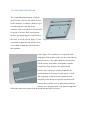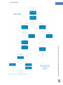
1
DESIGN AND IMPLEMENTATION
OF MANUAL ASSEMBLY CONTROL
SYSTEM
Raúl Quesada Navarro
Telecommunications technical engineer
Specialty in Sound and Image engineering.
Table of contents:
Table of figures: .................................................................................................................... 5
INTRODUCTION:................................................................................................................ 7
1.
PROJECT JUSTIFICATION: ...................................................................................... 9
1.1 BACKGROUND:...................................................................................................... 10
1.2 PROBLEM DEFINITION: ....................................................................................... 10
1.3 JUSTIFICATION: ..................................................................................................... 10
1.4 TARGETS: ................................................................................................................ 11
1.5 SCOPE AND LIMITATIONS .................................................................................. 12
1.6 STRUCTURE............................................................................................................ 12
2.
MECHANICAL DESIGN: ......................................................................................... 13
2.1 INTRODUCTION:.................................................................................................... 14
2.2 SOFTWARE: ............................................................................................................ 15
2.3 SENSOR CONTROLLER: ....................................................................................... 15
2.3.1 CONTROL BOX TOP ....................................................................................... 17
2.3.2 CONTROL BOX BOTTOM .............................................................................. 18
2.3.3 SENSOR BOX LEFT/RIGHT ........................................................................... 19
2.3.4 SENSOR GLASS ............................................................................................... 20
2.3.4 CONTROL PCB: ............................................................................................... 21
2.3.5 SENSOR/RECEIVER PCB: .............................................................................. 22
2.3.6 POSITIONING OF THE SENSORS ................................................................. 23
2.4 CONSOLE: ............................................................................................................... 24
2.4.1 BOX FRONT AND BACK................................................................................ 25
2.4.2. BOX TOP AND BOTTOM .............................................................................. 27
DESIGN AND IMPLEMENTATION OF MANUAL ASSEMBLY CONTROL
3
SYSTEM
2.4.3 CONSOLE PCB ................................................................................................. 28
2.4.4.
3.
OTHER COMPONENTS:............................................................................. 29
ELECTRONIC DESIGN ............................................................................................. 33
3.1 INTRODUCTION: .................................................................................................... 34
3.2 SOFTWARE: ............................................................................................................ 34
3.3 PREVIOUS CALCULATIONS ................................................................................ 35
3.4 SENSOR CONTROLLER ........................................................................................ 36
3.4.1 CONTROLLER BOARD:.................................................................................. 36
3.5 CONSOLE ................................................................................................................. 43
3.6 EMITTERS PCB ....................................................................................................... 46
3.7 RECEIVERS PCB ..................................................................................................... 48
3.8 WIRING: ................................................................................................................... 50
4.
SOFTWARE DESIGN ................................................................................................ 53
4.1 INTRODUCTION ..................................................................................................... 54
4.2.1 USER INTERFACE: .......................................................................................... 56
4.2.2 MENU OPTIONS AND CONFIGURATION PARAMETERS: ...................... 58
4.2.3 ASSEMBLY PROCESS AND SYSTEM LOCKING ....................................... 61
4.3 CONTROLLER FIRMWARE .................................................................................. 62
5.
PROTOTYPE AND PRODUCTION .......................................................................... 65
5.1 MECHANICAL PARTS ........................................................................................... 66
5.2 PRINTED CIRCUIT BOARDS ................................................................................ 68
6.
TESTS AND MODIFICATIONS ............................................................................... 69
6.1 PROBLEMS ON THE BASIC FUNCTIONALITY ................................................ 70
6.1.1 HOT PLUGGING AND NTC'S ......................................................................... 70
6.1.2 RESET PROBLEMS, WATCHDOG ................................................................ 70
6.1.3 CONNECTORS ................................................................................................. 71
Design and implementation of manual assembly control system.
4.2 CONSOLE FIRMWARE .......................................................................................... 55
6.1.4 IR LED EXCESSIVELY POWERFUL ............................................................. 71
6.1.5 ERROR IN THE PCB LAYOUT....................................................................... 71
6.2 FURTHER MODIFICATIONS ................................................................................ 72
6.2.1 CONNECTING MORE SENSOR BOXES ....................................................... 72
6.2.2 USING I2C PORT TO CONNECT WITH THE CONTROLLERS ................. 72
6.2.3 POSSIBLE WIRELESS COMMUNICATION ................................................. 72
6.2.4 SPI COMMUNICATION .................................................................................. 73
6.2.5 CHANGE TO ARM ARCHITECTURE ........................................................... 73
6.3 TESTS ....................................................................................................................... 73
6.3.1. TEST 1: ENCODER PROBLEMS: .................................................................. 73
6.3.2 TEST 2: THE CONSOLE GETS STUCK ......................................................... 74
6.3.3 TEST 3: IR LED'S RANDOMLY NOT WORKING ........................................ 74
6.3.4 TEST 4: SOME RECEIVERS NOT WORKING .............................................. 74
6.3.5 TEST 5: IR LED LIMITING RESISTORS HEATING IN EXCESS. ............. 74
6.3.6 TEST 6: DRIVING THE LED'S WITH THE TEST BURST. .......................... 75
6.3.7 TEST 7: DRIVING LED'S WITH LOWER CURRENT .................................. 75
6.3.8 TEST 8: LIGHT SOURCE INTERFERENCES ................................................ 76
7.
FLOWCHARTS .......................................................................................................... 77
8.
COSTS ........................................................................................................................ 93
8.1 DEVELOPMENT COSTS: ....................................................................................... 94
8.2PRODUCTION COSTS:............................................................................................ 97
DRAWINGS: .................................................................................................................... 101
Table of figures:
5
Table of figures:
Figure 2.3: Container with the sensors and controller already assembled. ......................... 16
Figure 2.1 ............................................................................................................................. 16
Figure 2.2 ............................................................................................................................. 16
Figure 2.4: Control box top, outside. ................................................................................... 17
Figure 2.5: Control box top, inside. ..................................................................................... 17
Figure 2.6 : Detail on control box. ...................................................................................... 17
Figure 2.7: Control box bottom, inner view. ....................................................................... 18
Figure 2.8 : Detail on control box bottom. .......................................................................... 18
Figure 2.9: Sensor box, left side. ......................................................................................... 19
Figure 2.10: Light transmission of the IR glass against wavelength. .................................. 20
Figure 2.11: Sensor glass. .................................................................................................... 20
Figure 2.12: Control PCB. ................................................................................................... 21
Figure 2.13: WAGO 733 series connector. ......................................................................... 21
Figure 2.15 : Reverse Gullwing LED .................................................................................. 22
Figure 2.16: JST-SMB11 connector. ................................................................................... 23
Figure 2.17 : Positioning of the emitters and receivers to avoid non-matched beam. ........ 24
Figure 2.18: Console box front, frontal view. ..................................................................... 25
Figure 2.19: Console box front, with assembled parts. ....................................................... 25
Figure 2.20: Console box front, top view, with assembled parts. ....................................... 26
Figure 2.21: Console box back, inner view. ........................................................................ 26
Figure 2.22 : Console box back, outer view. ....................................................................... 26
Figure 2.23: Console box bottom. ....................................................................................... 27
Figure 2.24: Console box top. ............................................................................................. 27
Figure 2.25: Top and bottom sides, including the PCB and the buzzer. ............................. 28
Figure 2.26: Console PCB ................................................................................................... 29
Figure 2.27: Locker, keyswitch. .......................................................................................... 29
Figure 2.28: 1602 LCD screen. ........................................................................................... 30
Figure 2.29: Keyes encoder module. ................................................................................... 30
Design and implementation of manual assembly control system.
Figure 2.14 Emitter PCB. .................................................................................................... 22
Figure 2.30: Button. ............................................................................................................ 31
Figure 2.31: Rocker switch. ................................................................................................ 31
Figure 2.32: C7 IEC power plug. ........................................................................................ 31
Figure 2.33: Buzzer ............................................................................................................. 32
Figure 2.34: Relay ............................................................................................................... 32
Figure 3.1: Console Schematic............................................................................................ 37
Figure 3.2: PIC18F4550 highlights. .................................................................................... 38
Figure 3.3: PIC18f4550 features. ........................................................................................ 38
Figure 3.4 : Controller PCB. ............................................................................................... 39
Figure 3.5: 2n7002 characteristics. ..................................................................................... 40
Figure 3.6: Console Schematic............................................................................................ 43
Figure 3.7: DIP switches. .................................................................................................... 45
Figure 3.8: Encoder turning counter-clockwise, two steps. ................................................ 46
Figure 3.9: Encoder turning clockwise, two steps. ............................................................. 46
Figure 3.10: Emitters PCB .................................................................................................. 48
Figure 3.11: Photoreceiver block diagram. ......................................................................... 50
Figure 5.1: Laser cut acrylglas. ........................................................................................... 66
Figure 5.2: FDM printed part. ............................................................................................. 67
Figure 5.3: Injection molding. ............................................................................................. 67
Figure 5.4: Pick and place machine. ................................................................................... 68
Figure 7.1: Menu structure. ................................................................................................. 78
Figure 7.2: Main function flowchart. .................................................................................. 79
Figure 7.3 : Main menu function flowchart. ....................................................................... 80
Figure 7.4: Configuration menu flowchart. ......................................................................... 81
Figure 7.5: Assembly menu flowchart. ............................................................................... 82
Figure 7.6: Assembly process flowchart. ............................................................................ 83
Figure 7.7: Determine box process flowchart. .................................................................... 84
Figure 7.8: Configure number of parts flowchart. .............................................................. 85
Figure 7.9: Flowchart of miscellaneous configuration options. .......................................... 86
Figure 7.10: Error handler flowchart................................................................................... 87
Figure 7.11: Flowchart of the process to check if all defined boxes are connected. ........... 88
Figure 7.12: Flowchart of several used functions. .............................................................. 89
Figure 7.13 : Flowchart of the main function of the controller. ......................................... 90
Figure 7.14: Sense and Toggle LED functions. .................................................................. 91
INTRODUCTION:
7
INTRODUCTION:
The following project, is the redesign of a former project ordered by a company to the
writer of this project, which wasn't totally successful on the first try, so it was a challenge
to find the way to make the system more robust and reliable, as close as possible to a real
commercial product.
In this project, there are three main fields which will be combined along it, electronics,
mechanics and programming. The mechanical design part, which was the main handicap of
the designer during the development of the project in which is based the following, will be
greatly improved. Also there was an improve in the electronic design skills, but over this,
the research and component identification of the designer have improved during the period
of time between the development of the old and the new project. Probably the part in
project, is the programming, but anyway the process of redesigning the system had as a
consequence in the designer to find a new way of thinking about the programming
problems and how to approach them.
It's important to note also the skills acquired regarding to the acquisition of materials, and
the relations with the providers.
Design and implementation of manual assembly control system.
which the designer didn't improve enough to mean a notorious change from the former
Design and implementation of manual assembly control system.
9
1. PROJECT
JUSTIFICATION:
1.1 BACKGROUND:
In several times , there were errors in the products acquired by the customers of the
company for which this system is being designed. Despite those errors are not big failures,
they result in products that must be replaced, with the consequent damage to the image of
reliability of the company, and the confidence of the customers on it.
Currently there is not any control system to identify any possible error in the manual
assembly process done by the workers.
Taking in consideration, the company for which this project is being built, wants to keep
the defect ratio under 10 parts per million, it's important to keep all the possible sources of
error, as controlled as possible, justifying on this manner, the following project.
1.2 PROBLEM DEFINITION:
Due to the lack of a control system on the manual assembly process, some distractions
made by the assembly workers, could give as a result, apparently correct assemblies, not
possible to be detected in the critical quality controls, but which can, in a short period of
time end up in a malfunction, giving as a result a problem in the offered services to the
final customer.
1.3 JUSTIFICATION:
To avoid the previously mentioned problems, and being able to guarantee better quality
and reliability to the customer of those assembled products (in the present case,
gearboxes) the perform of a control system on the parts the assembly workers utilize
during the assembly process is a must, ensuring any part is skipped or assembled in
incorrect order. Through this, the defective product ratio will improve, improving also the
productivity, and the customer satisfaction.
PROJECT
11
JUSTIFICATION:
1.4 TARGETS:
The targets of the current project are the following:
- Design the sensor system able to detect the movement of a hand inside the specified
boxes.
- Design the system to couple such sensors in a reliable way, to the specified boxes.
- Design the electronic circuitry needed in order to make the sensors work properly.
- Design the software needed in order to make the sensors work properly.
- Design the interface to connect such sensor system to a console, which will control the
overall assembly system.
- Design the console circuitry.
- Design the console software, in a such way that is intuitive and easy to use.
- Design the shape of the console in such way that is compact and reliable.
- Manufacture of a prototype.
- Write a User Manual.
- Provide technical support to the company whom acquires the system.
Design and implementation of manual assembly control system.
- Design an I/O interface, to be able to change the configuration of the system.
1.5 SCOPE AND LIMITATIONS
The scope of this project will be the utilization of the system in the assembly process inside
the assembly facilities of the company.
This system is not intended to be used outdoor.
This system is not intended to be used in areas with high ambient particles level (like
milling/machining facilities).
This system is a PROTOTYPE, so it may need further modifications to work properly, but
needs to be tested on the field for a long time to let the possible problems arise.
1.6 STRUCTURE
This project will be mainly divided into three different fields of interest:
- Electronic design.
- Mechanical design.
- Software design.
But will also include some other sections, but related in some way with those previously
mentioned topics, as the following:
- Prototype and mass production.
- System testing.
- Mechanical drawings.
Design and implementation of manual assembly control system.
13
2. MECHANICAL DESIGN:
2.1 INTRODUCTION:
Regarding to the mechanical design , the system has two differentiated parts, with their
own targets and limitations, the console and the controller.
Talking about the controller, the main needs are to design the housing to contain the
sensors, and the control logic unit, in a way that they get adapted to the chosen container,
minimizing the impact on the inherent functionality of the container, and letting use the
added functionalities with ease, and this means:
- Create a design which doesn't need to modify the container itself to be used.
- Design the housing on a way that adapts naturally the shapes of the container.
- Optimize the form factor.
- Allocate the connectors to the console in a way that allow easy access, avoiding to disturb
the normal workflow.
- Create a design which is easy to assemble and disassemble.
But also other needs as creating a mechanically robust design, which protects the sensors,
and to design on such way that the parts are easily manufacturable in long scale.
Moving now to the console, which is holding the human-computer interface, the
requirements are quite different, taking in consideration it doesn't need to get adapted to an
already existing external component. The priority on this case, is the ease to use, meaning
that the following:
- Locate the input devices in a way that is easy to access and use.
- Locate the output devices in a way they are easy to read, to provide the required
feedback.
- Give easy access to the connectivity to the controllers, as to the system output.
- Contain the electrical net connectors and switches to switch on and off the system.
Same as housing the power supply and the electronic circuitry related with the console,
and as in the case of the sensor housings the manufacturability will be taken in
consideration.
MECHANICAL DESIGN:
15
2.2 SOFTWARE:
The software to be used for the design of the mechanical components of the system will be
SIEMENS NX, due to the experience of the designer with the previously mentioned
software during his last job. SIEMENS NX is a powerful parametric mechanical design
software, which allows to easily reshape the different parts involved in a mechanical
design, through a complex system of relations between design features, and the use of
constraints over them. This software is also capable to manage high complexity assemblies
and the relation between them through constraints.
2.3 SENSOR CONTROLLER:
The sensor controller is at the same time divided in several subparts:
- Control box top
- Control box bottom
- Sensor box right
- Sensor glasses(right and left)
- Control PCB (which will be only briefly described regarding to the mechanical
characteristics due to the fact that this part belongs also to the electronic design section)
- emitters PCB.
- receivers PCB.
(These two last parts, will also have a brief description for the same reasons mentioned for
the case of the Control PCB).
Before the beginning of the description of the different parts, let's have a look to the figure
2.1 and 2.2, showing the container.
Design and implementation of manual assembly control system.
- Sensor box left
Figure 2.2
Figure 2.1
And a second picture containing the whole assembly:
Figure 2.3: Container with the sensors and controller already assembled.
17
MECHANICAL DESIGN:
2.3.1 CONTROL BOX TOP
The Control Box Top part, will be the one which covers the electronic control circuitry, it
will also have, as can be seen in figure 2.4, two hollows in which the connectors of the
electronic circuitry will fit, which use will be to connect with the console, and to have easy
access to debug/update the firmware of the sensor controller.
Figure 2.4:
2.5: Control box top, inside.
Figure 2.5:
2.4: Control
Control box
box top,
top, outside.
outside.
Figure
On the other side is also possible to appreciate the cavities and outgoings that will be used
The width of this part is determined by the size
of the chosen connectors, trying to keep it as
small as possible, not to disturb the form factor
of the container.
The thickness of the material will be kept in 1.5
mm, which gives robustness and flexibility,
without an excess of material use.
Figure 2.6 : Detail on control box.
Design and implementation of manual assembly control system.
for the fixation with the other parts comprising the sensor controller.(Figure 2.6)
2.3.2 CONTROL BOX BOTTOM
The Control Box Bottom part, will hold
the PCB and is also the one which fixes it
to the container, it contains a hollow to get
fixed through the back flap of the
container, and several holes to fix the PCB
by means of screws, those laying inside
the box, not disturbing the overall look of
the cases, as can be seen in figure 2.7 also
Figure 2.7: Control box bottom, inner view.
is possible to appreciate the profile of the
case, which is adapted to the backside of
the container.
On the figure 2.8 is possible to see again the little
outgoings which will be used to fix the control box to
the sensor boxes. The square hollows on both sides
will be used to insert them, and together with the
Control Box Top, will give the right fixation.
For the same reasons previously mentioned, the
overall thickness of this part is also kept to 1.5mm.
The outgoings, could represent a problem in the
simplicity of the design of a plastic injection mold,
Figure 2.8 : Detail on control box bottom.
because they could be seen as generating undercuts,
but they were designed with a size small enough that
allows the parts to be sprout from the mold with the help of ejectors.
MECHANICAL DESIGN:
19
2.3.3 SENSOR BOX LEFT/RIGHT
In the case of the sensor boxes, the design of both is the same, but inverted through the xaxis. So we will describe them together. Pay attention to the figure 2.9 to notice their
characteristics.
Figure 2.9: Sensor box, left side.
The interesting points about the design of this part are the following:
- The square on the left, to fix it to the Control Box Bottom and Top.
- The small keystone shaped cavities along all the part, used to fix the sensor glasses.
to get very deformed due to the injection molding process, and hold the sensor/receiver
PCB.
- Finally, There is a flap on the top of the part, with similar characteristics as the one in the
original container, with the finality of keeping the original functionality of the container
being able to stack several boxes even when they have the sensor system installed.
In this case, the overall thickness of the part is a little lower (1 mm) due to the need to
optimize the space, bound by the size of the PCB, which is determined by the size of the
connectors for the wiring of the emitters/receivers.
Design and implementation of manual assembly control system.
- The central pillar on the big cavity, which accomplishes a double function, avoid the part
2.3.4 SENSOR GLASS
The so-called sensor glass isn't really a glass, but a 1mm thickness sheet of acrylglass
named with the reference 9C20, which is transparent to a wide range of the IR light
spectrum, as is possible to notice in the figure 2.10.
Figure 2.10: Light transmission of the IR glass against wavelength.
This part is designed to be completely flat as can be seen on figure 2.11 to avoid possible
undesired reflections of the emitters, having also an added advantage for the manufacture.
The process to manufacture this part is slicing with a laser cutter, from a big dimensions
sheet. Is also possible to appreciate the keystone shaped outgoings, to fix it to the above
mentioned Sensor Box.
Figure 2.11: Sensor glass.
21
MECHANICAL DESIGN:
2.3.4 CONTROL PCB:
Figure 2.12: Control PCB.
the SENSOR BOX BACK, are the connectors:
- The blue ones are JST-SM11SB to match the connectors needed on the Sensor PCB, still,
those connectors don't contribute with any extra advantage to the PCB, in difference with
the case of the sensor PCB , so it's possible that they will get replaced, for other kind of
connectors.
The white connectors are WAGO
733-334 and 733-335, fitting on
those the plugs from the same
manufactured, with the reference
733-104 and 733-105.
The main advantage of using this
connector, is that they are 0.1
Figure 2.13: WAGO 733 series connector.
Design and implementation of manual assembly control system.
The spots of interest in the Control PCB, besides the screwing holes used to fix the PCB to
inch pitch, so is really easy to find other connectors which easily fit on them, also the
advantage of being able to exchange easily the wires attached on the 733-104/105 (see
figure 2.13).
2.3.5 SENSOR/RECEIVER PCB:
Those are the PCB's containing the emitters and the receivers themselves, the description
of such devices is out of the scope of this chapter, so it will be explained later, when
talking about the electronic design.
Figure 2.14 Emitter PCB.
Regarding to the mechanical design, the interesting aspects of
the PCB are those:
-The hollows in the PCB for the fixation with the sensor box,
the shape .
- The sensors, which are pointing through the PCB, using a
reverse Gullwing package, quite rarely used, so besides the
soldering pads of the sensors are on the side seen in figure 2.15
the sensors will be pointing through a hole on the PCB to the
sensor receiver PCB.
Figure 2.15 : Reverse
Gullwing LED
23
MECHANICAL DESIGN:
- Pay attention also to the connector,
which is the smallest form factor the
writer could
find to make it fit in
such a small space. The connector is
a JST-SM11SB, 11 contacts with 1
mm pitch.
Figure 2.16: JST-SMB11 connector.
Important to note, the distance between the sensors, which will be always, 23 mm for the
reasons explained in the section 2.3.6 due to the characteristics of the emitters and
receivers.
2.3.6 POSITIONING OF THE SENSORS
As will be easy to appreciate at the drawings 2.7 and 2.8 (where the emitters and the
receivers are shown), the distance between emitters is always 23 mm, same as the distance
to avoid the beam of the adjacent emitters over any sensors which is not the one the emitter
is pointing. Looking at the Datasheet of the VSMB2020, we can find the angle of half
sensitivity being 12º, which means an effective beam angle of 24º, as can be seen in the
figure 2.17.
Design and implementation of manual assembly control system.
between receivers, so they're pointing to each other. The reason to use this distance is to try
Figure 2.17 : Positioning of the emitters and receivers to avoid non-matched beam.
Anyways, after further experimentation, the designed realized that there are secondary
beams pointing to the receivers, thing that could be used as a feature to improve the
detection system if it's properly managed through software.
2.4 CONSOLE:
As mentioned before, holds all the electronics to interact with the device, the connectors
for the boxes, but also the power supply and the supply switch.
Let's show the parts that compose the console and the design limitations.
The components of the console are:
- Box Front
- Box Back
- Box Top
- Box Bottom
- Console PCB, comprising all the components fixed to it.
- Locker
MECHANICAL DESIGN:
25
- Screen
- Encoder
- button
- power plug
- power switch
- buzzer
- relay
2.4.1 BOX FRONT AND BACK
The Box Front and the Box Back are the parts in which all the components with outer
access will be attached, so in case of the front, it will contain holes for the locker, the
screen, the encoder and the button. It will also have four holes in the corners, to fix it to the
top and the bottom.
The back, will contain the holes for the power switch, the power plug, the connector for
four sensor controllers and the chain connectivity, which will be described in more detail
Figure 2.18: Console box front, frontal view.
Figure 2.19: Console box front, with assembled parts.
Design and implementation of manual assembly control system.
in the electronic design section. It also contains the same fixing holes as the front.
Figure 2.20: Console box front, top view, with assembled parts.
Figure 2.21: Console box back, inner view.
Figure 2.22 : Console box back, outer view.
Is important to note, in the first design phase, the connectors to the sensor controllers were
in the front side, giving easier access to them, but after thinking deeply on the usability of
the console, was decided to move them to the back side, so the wires are not interrupting
the easy access to the button, encoder and screen, which will become the center of the
interaction.
MECHANICAL DESIGN:
27
Both parts were designed using a flat surface, with the intention of manufacturing them
with a sheet of 3-4 mm plexiglass or plywood through laser cutting process, inasmuch as
the designer has access to such laser cutter for those materials, and is also a very easy and
cheap manufacture method (due to the lack of need of a mold, unlike in casting processes).
2.4.2. BOX TOP AND BOTTOM
The top and the bottom part will have a similar geometry, they will fit on each other,
housing all the console circuitry, and will be fixed through screws to the front and the back
side.
The bottom side will contain four plugs to fix the PCB through screws, in the same way,
Figure 2.23: Console box bottom.
Figure 2.24: Console box top.
Design and implementation of manual assembly control system.
the top side will have a couple of plugs to fix the buzzer.
Figure 2.25: Top and bottom sides, including the PCB and the buzzer.
2.4.3 CONSOLE PCB
Regarding to the mechanical design, the main point of interest is the location of the
connectors and the I/O devices. As much as can be directly attached to the PCB, as better,
so it will give robustness and reliability, but the fact is that is much more important to give
the right position to the I/O devices, so it becomes easy to interact with the system.
As can be seen in figure 2.25, the rear connectors, used to connect the console to the sensor
controllers, and the chain connector, used to connect to other machines part of the
assembly process, are the only components on the back side which are to be used outside
the housing of the console.
On the front side, the encoder is the only part which protrudes the console case.
29
MECHANICAL DESIGN:
All the rest of the components needed to be air wired, and connected to the PCB.
Figure 2.26: Console PCB
In the initial stage of the design, the connectors to the sensor controllers, were on the front
side, but once the wiring is connected, makes uncomfortable to work with the I/O devices,
All the rest of the connectors, were placed to serve internal device connection, like the
screen or the locker.
The size of the power supply (orange on figure 2.25) was in the initial stage of the design,
the most limiting factor for the size of the console.
2.4.4. OTHER COMPONENTS:
Locker:
The locker(figure 2.27), is a standard
SPST key switch, with a 19.5 mm
mounting hole, which can be provided by
several manufacturers. There isn't any
Figure 2.27: Locker, keyswitch.
Design and implementation of manual assembly control system.
and also implied to make the PCB much longer, the same way as the housing.
datasheet for this part, so it will be replaced in case of a further versions, to ensure the
technical characteristics.
Placed on the front panel to give easy access to the supervisors to change the options.
Screen:
This screen is a 1602 LCD, widely used along
consumer electronics devices, which can be
manufactured in very different sizes and shapes,
but most of them have the same dimensions, so
they're compatible with each other, the
dimensions are shown in figure 2.28 Placed at
Figure 2.28: 1602 LCD screen.
the center of the front side to make easy for the
users to read the displayed messages.
Encoder and button:
The encoder is a ready to use KEYES module,
easy to find on EBAY, probably based on a
TYCO DP12SV encoder. There are lots of
different encoder modules with the same
dimensions, so it is easy to find other models
which fit the same dimensions (figure 2.29).
Figure 2.29: Keyes encoder module.
31
MECHANICAL DESIGN:
The button is a 1662.0101 switch from
MARQUARDT, the dimensions of this button are a
de facto standard, so it's possible to find lots of other
buttons with the same dimensions (figure 2.30).
Both input devices are placed to interact with the
console, located on the right side, taking in
consideration most of the population is right handed,
should be easier to use (besides the designer is left
Figure 2.30: Button.
handed).
power plug and power switch:
The power switch is a so called rocker switch, there
are several different models with the same
specification, but in this case, the used one will be the
Figure 2.31: Rocker switch.
The power plug is a C7 IEC standard female
power plug. There are lots of different
manufacturers which provide this kind of
connector.
Keeping the switch close to the plug, it gets
clear is to switch off the machine, on the back
side.
Figure 2.32: C7 IEC power plug.
Design and implementation of manual assembly control system.
MARQUARDT 1801.1121.
Buzzer:
The used buzzer (Figure 2.33), is one of the
most common models used by the Arduino
community, which most probably will be a
PKM34EW-1101C/1201C from the
manufacturer MURATA .
This buzzer emits sound when some
operations are performed, if fixed to the
housing, will transmit better the vibrations.
Figure 2.33: Buzzer
Relay:
To connect to other devices related with the
assembly process. This device doesn't have any
kind of fixation because it could easily change
the shape and dimensions of the module, and at
the moment of the beginning of the
manufacturing from the PCB's this component
wasn't clearly determined. As can be seen in
figure 2.34, this is only a simplified indicative
Figure 2.34: Relay
model.
Design and implementation of manual assembly control system.
33
3. ELECTRONIC DESIGN
3.1 INTRODUCTION:
The electronic design part consists mostly in the design of the PCB and the choice of the
right electronic components for meeting the required characteristics given in the
specification, and given by the relations of the components between themselves, besides
this text is structured in a very linear way, this far away from a real design stage, which is
mostly iterative, in which the designer conveniently changes some to get adapted to other.
Also is the same with the relation between the mechanical design and the electronics
design.
So this is only the result of this iterative process.
3.2 SOFTWARE:
The software used for the electronic design during this project, will be EAGLE.
EAGLE is flexible expandable and scriptable electronic design application, with
schematic capture editor, PCB layout editor, auto-router and CAM and BOM tools.
Besides is not a very intuitive software, once a designer gets used to it, makes the design
fast and flexible.
The designer of this project will use the schematic and the layout editor for the
development of the electronic circuitry. Besides there are some scripts which allow eagle
to use simulation, they are quite complicated tools, not fully integrated in the software, and
most of the time the simulations need components to be replaced, which makes simulation
unworthy.
The main advantage of the EAGLE software is the existence of free versions for hobbyists
and students downloadable directly from CADSOFT.
ELECTRONIC DESIGN
35
3.3 PREVIOUS CALCULATIONS
Given by the specification there will be a maximum of 4 boxes, each of them will have the
same power consumption. The starting point will be a power supply of maximum 10W, to
try to design a non excessive consuming device. In case is not possible to meet the
specification using only 10W, the power supply will be resized.
So a safety margin for the power supply will be used, using only the 70% of the rated
value, which means maximum power consumption of the system 7W.
4 boxes with same power draw, we assign a maximum power draw per box to 1 W.
From the calculations related to the beam and the number of sensors needed to properly
detect a hand inside the container, we will get a total 8 emitters and 8 receivers, which
power draw was estimated to be a maximum of 0.5W for the emitters, 100mW for the
receivers.
The power consumption of the PIC is estimated to be 0.15W, through the measurement of
the power draw of other similar designs.
device, consuming 0.01W, almost negligible power draw.
Also the pull up resistors used for a possible I2C communication have a non-relevant
power draw.
Considering an efficiency on the power regulator which supplies the whole control board
of a 90% (this device is rated with a maximum efficiency of 95% on its sweet spot).
This means, in the worst case, we will be under the maximum assigned power
consumption, which is 1W per box.
Using 3.3 volts, the power draw will be considerably reduced, but this could cause
problems with the communication with the console, so this point should be revisited after
the device testing.
IMPORTANT NOTE:
Design and implementation of manual assembly control system.
The control PCB also contains a couple of LED's used to check the correct operation of the
Those were only rough calculations to have a first impression of the power draws needed
by the different parts of the system, to dimension the power supply and the regulator, but
the final design may differ.
3.4 SENSOR CONTROLLER
The sensor controller as its name says, will be in charge of controlling the sensors attached
to every container, besides all parts of the system together can be seen as a whole circuit, it
will be divided in three different parts, regarding to the division in different PCB's that has
been done in the system for mechanical reasons(to get properly adapted to the container)
and also thinking in the possibility of replacing some of the sensing modules for others
with different characteristics. Besides, as said there will be three differentiated parts, also
will be added a possible variation to one of them.
So the sensor controller will be divided in the following:
- Controller board:
Containing the control logic, the power regulation, and a power stage for the LED driving.
- Emitter board:
Containing the IR LED's used as emitters.
- Receiver board:
Having two different alternatives. First case, using phototransistors, second case using IR
receivers, the justification for this alternatives will be explained in the corresponding
section.
3.4.1 CONTROLLER BOARD:
Let us get started having a look to the final schematic design to point out the used
components:
ELECTRONIC DESIGN
37
Figure 3.1: Console Schematic.
As can be seen in the figure 3.1 The circuit contains:
- The microcontroller, at the center.
- A connector to the in-circuit programmer on the center top.
transistors needed to drive them to a higher current than the pins of the microcontroller can
supply, on the left side.
- Another connector for the receivers with pull down resistors for each sensor, on the left
side.
- The power and the run LED's, with its current limiting resistors, on the left bottom.
- A filter capacitor for the power of the microcontroller, also on the left bottom.
- The pull up resistors for the communication with the console, the power regulator, a filter
capacitor for the power regulator, and the connector to the console.
The microcontroller
As will be described in the further software sections, the device is a 8 bit microcontroller
PIC18f4550 from the company Microchip, here you can find listed some of its
characteristics:
Design and implementation of manual assembly control system.
- The connector to the IR LED's, the current limiting resistors for the LED's and the
Figure 3.2: PIC18F4550 highlights.
Figure 3.3: PIC18f4550 features.
So as can be seen in the figure 3.2 the 18f4550 has 35 I/O pins, from which we will need:
-8 pins for the activation of the IR LED used as emitters.
-8 pins for the sensing of the receivers.
-2 pins for the communication with the console.
-1 pin for the "run" LED, which will blink while the device is active.
There will be the need of using other IO ports which have a multiplexed functionality, to
use through them, the in-circuit programmer. Those pins need to be necessarily the pins
16,17 and 18, as can be seen in figure 3.3 which will not be available as IO.
ELECTRONIC DESIGN
39
Also the pins assigned to the communication with the console are fixed, to be coincident
with the I2C port of the microcontroller, regarding to a possible future modification to use
all the controllers unified in a single I2C bus.
Also can be seen the connection of some pins to a device called wireless. This device is an
NRF24L01 wireless communication module, which will not be described further, because
is a future modification out of the scope of this project, so it only be again commented in
the modifications section.
The pins where to connect the IR LED's and the photo-sensors, were chosen to be adjacent
and easy to route regarding the disposition of the elements in the PCB, as can be seen in
Figure 3.4 : Controller PCB.
Once the IR LED's and the sensors were correctly assigned to pins, then the rest of the pins
were chosen, so the final allocation of the pins became as seen in the schematic.
The connector to the in-circuit debugger:
Design and implementation of manual assembly control system.
the figure 3.4.
Contains five pins, according to the connectors that need to be done with the devices
pickit2 or pickit3 those pins are power, ground programming clock, programming data,
and master reset, to set the device in the programming mode.
The connector to the IR LED's
Already described and justified in the mechanical design section left to say that it contains
11 pins besides it needs only 10, to match the connector used on the side of the sensors.
The current limiting resistors for the IR LED's:
As their name explains are used to limit the maximum current through the LED's to its
maximum value, which is 100mA, its value needs to be adjusted depending on the final set
value of the power regulator, which could be 5 or 3.3 V, but the calculations will be done
taking in consideration the worst case, 5Volt.
Those resistors will never dissipate more than 0.25W, so it's possible to use common SMD
resistors.
The transistors, which will be of the type 2N7002, MOSFET topology transistors with this
characteristics:
Figure 3.5: 2n7002 characteristics.
The reason to choose those transistors is they are widely available, matched switching
speed for the application, power dissipation matching the application, not excessive on
resistance, no fixed voltage drop in the junction (in contraposition with the BJT topology)
and good price.
ELECTRONIC DESIGN
41
A capacitor to absorb possible voltage spikes that can generate unexpected behavior in the
microcontroller(more information about this can be found on the microcontroller
datasheet).
Connector for the receivers:
Same as in the case of the emitters (IR LED's), will connect to the receivers PCB, there's
also an extra pin which is connected to an analog pin, just in case it's needed in future
revisions.
Pull down resistors:
The pull down resistors, are set to be used with the phototransistors, and the system is
thought to use them as switches, which means, its value must be taken from the equation:
Vcc> R * Ia (being Ia, the value of the light current, and R the value of the pull down).
This gives a value of:
R > 5V / 6 mA , R > 866 Ohm.
In the case of the modulated photoreceivers , as it will be explained in the section 3.6, there
will be no need of those pull down resistors.
Power and run LED's:
If the system is powered on, the power LED, on this case white, will light up, if the
microcontroller is also active, the blue run LED will blink.
The maximum allowed current through the LED's is 20 mA (extracted from seller's
information) but taking in consideration there's no need to use the maximum brightness but
to optimize the power consumption, the maximum current will be set to 4mA. so the
resistors value will be:
Rlim = (Vcc - Vak)/ Imax
Rlim = (5- 3.2)/4mA
Rlim = 450 Ohm.
Design and implementation of manual assembly control system.
Anyway, this is only an indicative value, to use as start point for the test phase.
The chosen value will be the closest standard resistor value, 470 Ohm.
And the power consumption will be:
P = V*I
P = 5 * 4mA
P = 0.02W
Capacitor for the power of the microcontroller:
This capacitor is used to avoid high frequency ripple on the power of the microcontroller,
to avoid parasitic resets holding the power stable. The recommended taken the reference of
similar designs with a 18F4550 is 150 pF, but similar values will also work properly.
Pull up resistors for the I2C communication:
Those pull up resistors are placed to ensure the voltage reference on the communication
pins between the controller and the console, considering a possible future modification to
communicate both devices through the I2C protocol, two 4.7 KOhm resistors will be used,
which is a commonly used value for the I2C, taking in consideration the I2C bus will be
used only in low speed mode.
Power regulator:
The voltage supplied by the console is 12 Volt, to transmit more power with less loses
through the wires which connect the console and the controller, but the voltage needed for
the controller circuitry is from 3.3 to 5 Volt, so there's a need for a step down voltage
regulator.
In this case, the voltage regulator will be a MINI 360 step down switching regulator,
which is able to convert a voltage up to 23 Volts to a lower voltage, as low as 1 Volt, so it
will be able to deliver both 3.3 and 5 Volts to the controller circuitry, just setting up the
right value with the potentiometer included on the regulator. This circuit also shields the
partially the possible voltage drops on the console to affect the controller circuitry.
ELECTRONIC DESIGN
43
(IMPORTANT NOTE: the regulator is set to its maximum value by default, so it MUST
be tested and calibrated before soldering on the PCB or it may cause damage to the
circuit).
Filter capacitor for the power regulator:
Used to hold the voltage stable on the controller side , in case of abrupt changes on the
power consumption.
3.5 CONSOLE
Let us proceed with the console in the same way done with the controller, starting with the
Figure 3.6: Console Schematic.
As can be seen in the figure 3.6 The circuit contains:
- The microcontroller, at the center.
Design and implementation of manual assembly control system.
schematic, to show the different parts of the design.
- A connector to the in-circuit programmer, the power and the run LED's, with its current
limiting resistors, with the recommended capacitor for the microcontroller power supply on
the center top.
- On the left side, can be seen the connections to the four controllers, and also some
switches, which will be used to reconnect the pins of the boxes to the I2C port, feature that
could be used in future versions.
- At the right side on the top, can be seen the power supply, and a voltage regulator, plus
the connector to the power plug.
- Below those, can be found the I2C port connection, used for the communication with the
1602 LCD.
- At the bottom, on the left side there are the connections used for the external switch, used
to connect to other devices of the manufacturing process, from here and so on called "chain
out."
- Moving to the right, we find the connections to the buzzer, which will be connected
through a transistor, just in case there's a need to change the chosen buzzer for a more
powerful one.
- Moving again to the right, we find the connection to the button.
- Finally on the right side at the bottom, the encoder and its additional circuitry can be
seen.
The microcontroller:
The microcontroller of the console is the same as in the controller board, and its features
are the same as described in section 3.3 (sensor controller).
The pins for the different devices attached to the microcontroller, were chosen to get a
good distribution on the PCB, unless those that needed to be connected to specific pins,
like the I2C port pins, and the Pickit In-Circuit-Programmer.
Connectors for the controllers:
They will be WAGO 733-334, as described in the section 2.3.4, Control PCB.
Each of those connectors consisting in 4 pins will be have the first and the last pin
connected to the 12VDC power rail, and to ground respectively, whereas the other pins
will be for the communication between the console and the controllers.
45
ELECTRONIC DESIGN
DIP switches:
Those are 8 contact 0.1 inch switches which
will be used to conmute the functionality
between dedicated ports to I2C bus for the
controller boxes. While all of the switches of
one package are on, all the switches on the
other package must be off.
Figure 3.7: DIP switches.
Power supply:
The power supply will be a VIGORTRONIX 214-010-112 which will convert the
230VAC from the net in 12VDC used to deliver the power to the sensors, which will be
afterwards converted in 5 VDC to power the circuitry of the console.
I2C Port and 1602 LCD:
WAGO 733 series connector, the console circuitry will connect to the 1602 LCD, used to
display information to the users. The LCD has an external circuitry attached to it, allowing
to communicate by means of I2C protocol. The drivers for this device, were written for
another project by the designer of this project.
Switch and encoder:
Used as input devices from the user, they have some extra external circuitry to perform a
HARDWARE DEBOUNCING to avoid multiple detections due to the mechanical parts
contained in the button and in the encoder.
The encoder is a QUADRATURE DOUBLE STEP rotary encoder. In the figures 3.8 and
3.9, can be seen the signal generated for this encoder while rotating clockwise and anticlockwise.
Design and implementation of manual assembly control system.
Through this connector attached to the I2C port of the microcontroller, which will also be a
Figure 3.8: Encoder turning counter-clockwise, two steps.
Figure 3.9: Encoder turning clockwise, two steps.
From this graphs, taken with a logic analyzer, the designer programmed the driver to use
the encoder as the input device for the console.
Other:
All the non described items, have the same characteristics as in the section 3.3.
3.6 EMITTERS PCB
The emitters PCB will consist in the IR LED's, and the connector to the controller. The
description of the connector was already given in the section 2.3.5, so there's only left to
talk about the LED's which are VSMB2000X01, some of its characteristics are:
- Peak wavelength 940 nm (infrared range).
- High radiant power.
- Angle of half intensity 12º.
- Dimensions 2.3 x 2.3 x 2.8.
ELECTRONIC DESIGN
47
And those were the main reasons to choose this IR LED, to keep the form factor of the
device as small as possible there was a need of small devices, and was important to keep
the angle of the beam as small as possible to avoid interferences with the receivers. The
anode of the IR LED's is connected to Vcc, while the cathode is connected to the drain of
the FET's from the controller unit, so when the FET's are active the cathode gets connected
to ground and the current flows, limited by the current limiting resistors.
So let's check the power consumption of the emitters:
Taking this data from the datasheet:
- IF(max) = 100mA (IFM(max = 200mA)) maximum continuous forward current and peak.
- Vfmin = 1.15V
if the Voltage supplied to the LED's is 3.3V:
VCC = 3.3V, VF = 1.15V
so Rlimit = ( vcc- vf)/Imax = (3.3 - 1.15)/0.1 = 21.5 Ohm
and then Prlim = I^2*R = 21.5*0.1 ^2 = 0.215 W
added to Pled = V*I = 1.15*0.1 = 0.115 W
So the power draw for each LED and resistor is = 0.330W
maximum, the same as one LED active all the time.
In case the voltage is 5V:
VCC = 5V, VF = 1.15V
so Rlimit = ( vcc- vf)/Imax = (5 - 1.15)/0.1 = 38.5 Ohm
and then Prlim = I^2*R = 38.5*0.1 ^2 = 0.385 W
added to Pled = V*I = 1.15*0.1 = 0.115 W
So the power draw is = 0.5W
The emitters will be switched through transistors, which power consumption should be
also considered. The chosen device is the 2n7002, which an internal on resistance of 5
Ohm.
Design and implementation of manual assembly control system.
Two LED will never be active together, so it means the power draw of all LED's will be
As before said, the maximum current through the emitters will be 100mA, which gives a
value for the power consumption of:
P = I^2*R
P = 5*0.1^2
P = 0.05W
Figure 3.10: Emitters PCB
3.7 RECEIVERS PCB
From the beginning, the system was thought to be tested with 2 types of sensors, so we will
get the calculations for both of them.
- Option with phototransistors:
Taking in consideration the calculations shown in the corresponding section, the maximum
power consumption will be 25mW per phototransistor, what means 200mW total.
- Option with photo-receiver:
The power consumption of this device comes directly extracted from the datasheet, and is
10mW per device, making a total of 80mW.
ELECTRONIC DESIGN
49
Phototransistors:
There are two different ways to use phototransistors, as a linear device, and as a switching
device. This depends on the voltage supplied, an own characteristic of the phototransistors,
called 'collector light current', which defines the maximum current through the
phototransistor for the maximum lighting, and the voltage applied.
The rule to define one or other mode is the following:
Vcc > R*Ica --> we never get into the saturation area, so it works as a linear device.
Vcc < R*Ica --> at maximum luminosity we are saturated. So the formula to calculate the
proper resistance will be:
R > Vcc/Ica
Using this formula, with our given values(Ica = 6mA, Vcc = 5V):
R > 5/0.006 = 833 Ohm
This is the minimum value to get into the saturation area with the maximum luminosity
detectable by the phototransistor, but by setting bigger the value of R, is possible to switch
the phototransistor at lower values of luminosity. To set the proper value for the
application, some tests should be done, but an approximate value of 1KOhm will be taken
The two problems that can arise through testing are:
- The LED is not bright enough to saturate the phototransistor (there's a need of a more
powerful LED).
- The environmental light saturates the device (reducing the value of the resistor could
solve this)
Take in consideration a possible variation in the voltage to a 3.3V power source, which
means:
R > 3.3/0.006 = 470 Ohm, so with a 1kOhm resistor we will get in the saturation area at
the half of the maximum luminosity of the phototransistor.
Design and implementation of manual assembly control system.
for the first tests.
Photoreceivers:
The photoreceivers, are slightly more sophisticated devices than the phototransistors, and
include generally a block diagram as the one in figure 3.11.
Instead of just sensing the IR light level, the IR receivers, need a modulated IR signal to be
excited, this has some advantages, for example, IR noise light immunity, but also means
the emitters need to generate this modulated signal.
Figure 3.11: Photoreceiver block diagram.
As can be seen on the block diagram the system has integrated pull up resistors, so there's
no need for external ones, which will not be soldered in the control PCB when used with
photoreceivers.
The device used for this project will be the TSOP77436, which has a modulation
frequency of 36KHz
The power consumption given by the datasheet of the device is 10mW, what means a
maximum of 80mW when all 8 receivers are powered. Below the previously maximum
consumption expected, which was 100mW.
3.8 WIRING:
The wiring between the sensors and the controller, but also the wiring used to connect the
controllers to the central console is something to take in consideration.
ELECTRONIC DESIGN
51
Due to the limitation given by the connectors used (SHR-11V-S), the wire to be used, for
the sensor-controller connection, will be the recommended by the manufacturer of the
connectors, which is in the range of AWG 32 to AWG 28.
The position of the different pins on both PCB's were chosen to be able to crimp the wires
with a simple correspondence, meaning this, that the pin number in the sensor PCB and the
control PCB is the same, or inverted, so the last pin on the receivers, correspond to the first
pin on the console, and vice-versa. This is an important fact, so it will be easier to find
already crimped wires following this specification, than a random disposal of the pins. This
will also reduce the manufacturing costs.
For the case of the wires which connect the console and the controllers, the connectors
were chosen to be able to replace the wiring with ease, so the company which acquires this
project, can exchange them depending on their needs. Right now, the designer is using
Design and implementation of manual assembly control system.
1.27mm pitch 4 poles ribbon cable.
Design and implementation of manual assembly control system.
SOFTWARE DESIGN
53
4. SOFTWARE DESIGN
4.1 INTRODUCTION
There will be two main parts in the software design, one regarding to the console, and the
other on regarding to the sensor controller.
The chosen microcontroller for this development is the PIC18f4550 from the company
Microchip. The reason to choose this microcontroller is the wide previous experience of
the designer with this microcontroller.
The software chosen for the development is the MPLAB X Integrated Development
Environment provided for free by microchip. The advantage of using this IDE instead of a
generic one, is the full integration with the microcontroller programmers Pickit2 and
Pickit3 available for the designer, also its code autocomplete capabilities, and multiple file
structure organization, also the compatibility with several different compilers, like CCS,
C18 or XC8.
The compiler of choice for the previous development of this project was C18, but during
the redesign process, the designer decided to change this compiler for a more updated
version, which is up to date, in difference with the C18 compiler which is currently
deprecated for new projects, and no more technical support provided.
The XC8 compiler is based on the ANSI C standard, with the addition of several specific
libraries for the use of each specific microcontroller architecture from microchip, so is
possible to access all the peripherals of every device through C libraries, instead of having
to program them through assembler code.
SOFTWARE DESIGN
55
4.2 CONSOLE FIRMWARE
The main tasks of the console firmware are:
- Configure and manage the user interface, which consist in several input and output
devices to be controlled by the user, or to display information to acknowledge the user.
- Give access through the user interface, to all the configuration parameters to be used in
the different assembly types.
- Control the assembly process, meaning this, to check if the assembly workers take the
- Block the assembly system in some way, not allowing the assembly workers to continue
with the process, before the supervisor checks the assemblies which could give place to an
error.
Design and implementation of manual assembly control system.
right amount of parts and on the right order to get a correct assembly.
4.2.1 USER INTERFACE:
Those are the input devices the users can access to:
Encoder with button:
Turning this device right or left, the user can go through the different menu options,
pushing the button contained in the encoder starts the selected process for example to start
the assembly process, or to change the configuration parameters.
Secondary button:
Pushing the button returns from the current option back, stopping the process without
saving any information changed. Together with the "Encoder with button" is enough to
move back and forth through all the console options.
Locker:
The locker is used to avoid the assembly workers to change the different configuration
options, so once the locker is closed, all the configuration functionality disappears from the
console options.
The menu options are intended to be only user by the supervisors, to properly set up the
machine, and to unlock it in case there's any mistake in the assembly.
SOFTWARE DESIGN
57
And those the output devices:
Screen:
Used to display most of the relevant information of the system, also to navigate through the
different options. Most of the screen handling is hidden in flowcharts, due to the fact the
libraries used to manage such events, were programmed by the designer, but are generic
for different projects, so they're out of the scope of this text.
Power LED:
Simply a white LED, which shows the system is already powered on.
Run LED:
Colored led which blinks while the microcontroller is performing tasks, so if the LED
stops blinking means the system got stuck. Useful for debugging tasks, but also just in case
there's a critical error during the process, the user can appreciate the machine is stuck, and
restart it.
Used during the assembly process, to acknowledge the assemblers the detection, and also
to be used as an alarm when there's a fail in the assembly process.
Chain(relay):
The designed console, could be connected also to other devices that are checking other
parts of the assembly process, and this is the way they communicate. When the contact
change from its normal state, it means there's a problem in the process, and it will only
return to the original state, when the supervisor unlocks the system through the locker.
Design and implementation of manual assembly control system.
Buzzer:
4.2.2 MENU OPTIONS AND CONFIGURATION PARAMETERS:
All the configuration parameters explained in this section, will be stored in global
variables, so there's easy access to them from any part of the program.
In the figure 7.1 can be seen the different options through which the user can navigate.
Let's get a little bit more in detail about those options:
4.2.2.1 Firmware version
Allows you to check the current firmware version installed in the device, in case the
company which ordered the project decides it on that way, this could be changed to a text
displaying the name of the company or any other text.
4.2.2.2 Assembly start
Shows on the screen the possibility to start the assembly. pushing the enter button starts the
assembly process.
4.2.2.3 Assembly
Once here we are inside the assembly process itself, and it will be ruled by the flowchart
attached within the figure 7.6.
4.2.2.4 Configuration menu
Allows the user, by pressing the 'enter' button to get inside the configuration menu, letting
the user move through the different options.
Attention!
The Configuration menu is not intended to be used by the workers involved in the
assembly process, but for the supervisors, so this menu will be hidden while the locker
stays open.
SOFTWARE DESIGN
59
4.2.2.5 Configuration option display
The options going from 'NUMBER OF BOXES' to 'ERROR STATISTICS' are an
intermediate step to get into the actual configuration process, used to display the
corresponding name. Regarding to their functionality they can be grouped all together.
4.2.2.6 Configure Number of boxes
This option allows the user to change the number of boxes the system will use in a specific
assembly, each box represents a different part. The current system will have capability for
up to 4 different parts, but it could allow up to 8 boxes with the current console hardware,
and up to 16 doing minor design modifications. Those modifications will be done only
under demand.
Turning right or left will increase or decrease the number of boxes, pushing 'enter' will
save the current value, 'back' will leave the menu without saving.
The maximum value of boxes will be kept in the range before defined.
4.2.2.7 Configure parts per box
Through this menu option, the user will be able to decide how many equal parts will be
'Up' and 'Down', will increase/decrease the number of parts in the currently displayed box.
'Enter' will move to the next box. Once in the last box, it will quit automatically. 'Back' will
quit the configuration menu without saving the currently displayed number of parts.
4.2.2.8 Time between boxes/inside box
Used to determine the timings the assembly workers can stay idle without taking the next
part of the assembly.
The behavior of this configuration will be the same as the previously explained in the
section 4.2.2.6 , but with a different maximum and minimum ranges.
4.2.2.9 Sound
Allows to set the alarm sounds active/inactive depending on the preferences of the user.
'Up' and 'Down' will toggle the option, whereas the 'Enter' button saves the option and
quits, and the back button quits without saving.
Design and implementation of manual assembly control system.
used in the assembly(extracted from the same box).
4.2.2.10 Error Statstistics
Inside this option is possible to check the number of faults committed after the last counter
reset. To reset the counter turn the encoder left, turning right has no effect, 'Enter' and
'Back' options share the same behavior, going back to the configuration menu.
note: In future versions of the software there will be several other error statistics.
SOFTWARE DESIGN
61
4.2.3 ASSEMBLY PROCESS AND SYSTEM LOCKING
The assembly process, which is the main aim of the design, is thought to proceed as in the
flowchart given in the 7.6, but let us explain it normal language:
Once the machine is switched on (with the locker closed), the only available options are
the firmware, and the assembly start, pushing 'Enter' on the assembly start options, the
system will show the number of a box, from which the worker needs to extract a part, and
it will continue showing the same box number until, as many parts as needed for the
assembly are extracted. Then the number of box will change, and the worker should then
repeat the process with the box with the corresponding number shown in the screen.
Once all parts from all boxes are extracted, the process starts again.
If there's a detection in a box which is not the one shown, or there's a try of a simultaneous
extraction from several boxes, the system will display the error and get locked.
In case the time assigned to extract the part from the box and assemble it expires, or the
system is detecting a hand/object inside the box for too long, the system will behave in the
Once the system is locked, the it will change the state of the relay, locking also the other
processes in the assembly chain. Then, the system will keep locked until the supervisor
unlocks it using the provided keys for the electric locker. Then, the worker will be able to
start the assembly again.
Design and implementation of manual assembly control system.
same way as before mentioned.
4.3 CONTROLLER FIRMWARE
The goal of the controller firmware, is to generate the proper signal on the emitters to
excite the receivers, and to capture the value of the receivers, so is possible to know if
there's any cut on the beam between the emitter and the receiver. This is the basic way to
find out if there's any interaction inside the boxes. This method starts being quite simple,
but it will be subject to changes, to improve its reliability.
This process should also toggle, from time to time, the RUN LED embedded on the PCB,
to easily detect the proper function of the microcontroller.
To try to get a better detection, there are some characteristics to remark, to clarify the some
of the characteristics of its function.
The receivers work with 36MHz light, what means there's a need to generate at the LED's a
signal with the same frequency to excite them. This will be defined as a burst.
Given the information on the datasheet, it's not possible to emit continuously over the
sensors, or they will lose their sensitivity, what means there will be a pause between bursts.
When there isn't any strange object (like a hand) inside the container, the receivers get the
light from the IR diodes, but in a multiplexed way, what means, each of the detectors
receives a burst, pauses, and then the next detector repeats the same process in a
continuous cycle. So, during the time the IR LED is emitting directly to the receiver, in the
case there's nothing cutting the beam, its output level will be LOW. and HIGH during the
rest of the time to perform a full multiplexed cycle.
So the moment to detect if there's a cut on the beam, meaning this a strange body inside the
container(like a hand, for example) is while generating the burst. (This process is also
documented in the figure 7.12)
Every time the IR LED gets high, to generate the burst, the output of its corresponding
detector will be checked, and a variable will be increased if the receptor is low.
SOFTWARE DESIGN
63
If after finishing the whole burst, the saved variable goes over a predefined threshold, it
will count as a positive object detection.
Once there's a positive detection, the cable connected to the central console will get high.
The system will continue sensing for a positive detection, while holding the console cable
high. At the point the sensing gives as a result a negative in the detection, the system will
wait for a defined time, expecting a second negative detection to pull down the console
communication pin. This pause and double check, is a way to debounce the sensor system.
As can be seen in the figure 7.12 the LED blinks every defined number of detection cycle,
defined by the variable max in the LED toggle flowchart. This means, the LED isn't
Design and implementation of manual assembly control system.
blinking on a fixed timing, but depending on the timings of the sensing process.
PRODUCTION
Design and implementation of manual assembly control system.
65
5. PROTOTYPE AND
5.1 MECHANICAL PARTS
To check the proper functionality of the parts, as a part of the redesign of a system is
important the use of prototypes. The prototypes manufactured for this project, are done
with two different systems, laser cut parts, and 3D printed parts.
Laser Cutting:
The laser cut manufacturing, is usually used with
parts which have a flat dimension, so they can be
produced by cutting them away from a raw sheet of
material. It's possible to get the parts directly from the
machining provider, or to get the raw material and
pay the laser cutting service per given time. In the
case of this project, the designer had the access to a
Laser cutter, and had the knowledge to use it, so the
prototypes were manufactured in a timed service.
The parts prototyped with this method are "console
box front" and "console box back".
Figure 5.1: Laser cut acrylglas.
In the case of a mass production, is always better to outsource the service and relay in the
hands of professionals, it will be easier and cheaper.
3D printing (FDM):
The definition of 3D printing, is a vague conglomeration of very different manufacturing
techniques with something in common, they're additive techniques, and this means that,
instead of removing big quantities of materials from a raw block, they add small quantities
until the desired part is generated.
Three examples of these techniques are:
- SLA(Stereolithography):
which uses a laser to cure a photosensitive polymer, by layers, a slow method with very
few and expensive material choices, but good print quality.
67
PROTOTYPE AND PRODUCTION
-SLS(Selective Laser sintering):
Generates the part melting selectively polymer dust. Giving parts of good quality, small
tolerances, but rough surface finish.
-FDM(Fused melted deposition):
The additive manufacturing most diffused method, using an
extruder to melt a plastic filament which conforms the parts. It's
a method with low reliability and low quality prints, but is far
away the cheapest, in terms of machinery and material.
This will be the method used for the production of the following
prototypes.
"Console box top", "console box bottom", "control box top",
"control box bottom", "sensor box right" and "sensor box left".
Figure 5.2: FDM printed part.
Injection molding:
For a possible mass production, the preferred production
molding. This has some implications on the mechanical
design of the parts, like minimizing the undercuts, and
draft all the parts to ensure the demoldability. Those and
other requirements can be seen on the included offers,
used also for the costs estimation.
Figure 5.3: Injection molding.
Design and implementation of manual assembly control system.
method for the 3D printed prototyped parts will be the injection
5.2 PRINTED CIRCUIT BOARDS
Gerber files:
The first step to manufacture a PCB, usually is to get from your preferred PCB design
software, the GERBER files, which is a de facto standard for the PCB production. Usually
there's also the need to add the Excellon files, which refer to the drilled holes.
PCB Manufacture:
Once the CAM files are ready, there are lots of different online service in which you can
manufacture the PCB's, for this project, the designer checked several services around
europe and asia, and besides the wish of the designer to manufacture the PCB's in the EU,
but the price difference is so humongous comparing to the Asian market, that was
impossible to the designer to afford EU manufacture.
Hand soldering:
For the prototypes, the part assembly process and soldering was handmade, due to the
excessive cost for a small production through other methods like the pick and place
system.
Pick and place:
The pick and place systems, are the preferred for a
medium to high production quantities, it gets
discarded for the prototypes due to the high initial
costs of the technology. Those systems
automatically place all the components over the
PCB, which will be afterwards soldered inside a
PCB oven. Let us see an example of this machines
in the figure 5.4.
Figure 5.4: Pick and place machine.
6. TESTS AND MODIFICATIONS
Design and implementation of manual assembly control system.
TESTS AND MODIFICATIONS
69
6.1 PROBLEMS ON THE BASIC FUNCTIONALITY
6.1.1 HOT PLUGGING AND NTC'S
In lots (but definitely not in all) modern electronic systems, is possible to directly plug
some parts of the device while it's connected and working. This action is known as hot
plugging. When designing the device described on this project, it was never taken in
consideration, but simply expected to work on this way.
If plugging directly the sensor boxes onto the console, the power draw of the boxes, and
the connection process itself, generates large voltage and current spikes, which generate
resets on the microcontroller of the console.
To avoid this kind of behavior and enabling a real hot plug system, the use of NTC's in
series to the power pin which goes to the different boxes, will make the current to be small
when the boxes are connected, and while the heat on the NTC's increase, their resistance
will go down, letting the current rise slowly until a stationary state, in which the power
draw of the NCT will be negligible.
6.1.2 RESET PROBLEMS, WATCHDOG
There are lots of different reasons why a microcontroller can get stuck, As explained in the
previous section big variations in the power draw, generating current spikes is one of them.
But also for example, a close device, generating EMI (electromagnetic irradiation) or a bad
code, could paralyze the microcontroller. To avoid that, there's a special device on the
microcontrollers called watchdog, which can generate an automatic reset on the
microcontroller on a regular time basis, when it's timer is not software reset. This is a
fantastic method to get a reliable device, but it requires to structure the code in some way
which allows to perform all the tasks before the watchdog timer overflow.
Unfortunately, the code wasn't properly structured for it, and the designer doesn't have the
71
time to modify the code before the first release, but will probably be modified in case
there's a second release.
6.1.3 CONNECTORS
During the testing phase, some problems with the IR LED shown up, they were randomly
working depending on the position of the PCB, which in the beginning look like a crimp
problem, the designer had to crimp all the wires on his own, with tools which were not
adapted to this kind of connectors, which is an inherent focus of troubles and errors, but at
the time, it was simply the only possible option. Finally emerged the real cause of the
problem, which was a bad solder, another of the most common problems, due to the hand
soldering of very small components done by the designer.
6.1.4 IR LED EXCESSIVELY POWERFUL
On the calculations for the current draw for the LED's was taken the maximum possible
brightness of those, thinking that this would be the best option to improve the reliability of
the beams, but several problems came into view.
The excess of power of the LED's were causing lots of reflections inside the containers,
There's a consideration ignored before, which is the fact that HUMAN FLESH IS
ALMOST TRANSPARENT TO IR LIGHT. What means there's a need to emit at very
small power, so the goal of detecting a hand inside the containers is accomplished.
6.1.5 ERROR IN THE PCB LAYOUT
There was an error in the footprint of the VTX-214-010-112 device, the issue was the
footprint was mirrored, so the power supply could be properly connected on the other side,
the problem is, doing so, means the dimensions of the PCB change totally, making
impossible to fit inside the console box.
This problem was solved soldering wires to the power supply to replace them on the solder
of the PCB.
The proper way to solve this problem would be to modify the footprint and redesign the
CPB, but there was no time to wait for the manufacture of the new board, so the designer
of this project decided to go forth with the current PCB design.
Design and implementation of manual assembly control system.
which meant that all the receivers were active every time an LED was flashing.
6.2 FURTHER MODIFICATIONS
6.2.1 CONNECTING MORE SENSOR BOXES
There is the possibility to connect more sensor boxes performing a modification in the
software and adapting the wiring between the console and the controllers, using the second
I/O pin every box port has available, currently used to ensure the boxes are connected.
6.2.2 USING I2C PORT TO CONNECT WITH THE CONTROLLERS
This possible modification was taken in consideration from the beginning of the design of
the PCB's so by means of the internal DIP switches on the console PCB is possible to
connect all the controller box ports to the console, in a way that they can make use of the
I2C port communication. This feature wasn't tested due to the lack of time before the
deadline of this project.
One of the expected problems of this method, will be the maximum allowed wire length,
which depends on the value of the pull-up resistors used on the I2C data and clock pins,
and the length of the wire used by the communication. Decreasing the speed of the clock
signal, will also improve the reliability of the communication.
6.2.3 POSSIBLE WIRELESS COMMUNICATION
A possible wireless communication between the sensor controllers and the console was
taken in consideration, adding to the controllers a Lithium Polymer battery, could avoid the
need of wiring the system, giving a much better flexibility.
It's possible to notice the footprint of and NRF24L01 on the controller PCB, which was the
device intended to be used for that communication. Due to the high power consumption
reduction on the IR LED's commented in section 6.1.4, this option is much more feasible,
so if there's a redesign on the project, will be oriented on this way.
73
6.2.4 SPI COMMUNICATION
The previously mentioned NRF24L01, communicates to the microcontroller through SPI
port, which in the actual microcontroller isn't compatible with the I2C communication,
which implies to change the communication protocol between the LCD screen included in
the console, and the microcontroller to I2C, this can be easily done using another PCB
previously designed, just replacing the I2C for the SPI module on the back side of the
screen.
6.2.5 CHANGE TO ARM ARCHITECTURE
The change in the architecture of the microcontroller, is one of the most critical possible
changes, because it will imply a very deep redesign in the project, but if the time would be
available, this modification can represent the biggest performance improvement of the
system(not functionality improvement, which will be the wireless communication system.)
6.3.1. TEST 1: ENCODER PROBLEMS:
The encoder used for the very first development differs from the currently used. The driver
for the encoder, was developed for the former encoder type, so there's a need of modifying
the encoder driver to use it with the new model.
After trying to approach the problem in several different ways, gets clear that the
modifications to be done, need to be much bigger than expected, declining the designer to
make those modifications before the deadline. This modifications could be done when rewriting the console software in a possible next revision.
Besides not totally correct, the console still useable, with some modifications on the
encoder driver.
Design and implementation of manual assembly control system.
6.3 TESTS
6.3.2 TEST 2: THE CONSOLE GETS STUCK
The console gets stuck randomly from time to time, to solve this there will be a plan to
readapt the code to use the watchdog in the next revision of the software, currently not
implemented, making the system less reliable.
6.3.3 TEST 3: IR LED'S RANDOMLY NOT WORKING
Using IR light for the development of the sensors, means it's not possible to check the
proper function of the LED's just looking at them, for all the checks done to the IR-LED's
was necessary the use of a mobile phone with camera, taking the advantage to the fact that
most of the camera sensors are sensitive to IR light.
While testing the controller for the first time, the IR LED's weren't working at all. After
some time looking for the problem, they randomly started to work. Finding the problem
took quite long time, during which some other tests were performed, until the system
started to fail again. Finally was found out that the problem was due to a cold solder, made
in the pins of the connector of the IR LED's PCB.
6.3.4 TEST 4: SOME RECEIVERS NOT WORKING
The first point to check if the receivers are working properly is to check if they have their
outputs high when no infrared modulated light is emitted on them. Checking with the
multimeter it emerged that 3 of the outputs weren't high. After checking the conductivity of
some tracks on the PCB, was found out that some pins of the sensor weren't in contact with
their pads, due most probably to a cold solder. After re- soldering the faulty sensors, were
tested again, giving the right values.
6.3.5 TEST 5: IR LED LIMITING RESISTORS HEATING IN EXCESS.
To check the code of the controller for the first time, and to be able to clearly see through
the camera the IR LED's were working, the LED's were flashing without modulation,
which means they were always active, obligating the LED's and their limiting resistors to
dissipate much more power, heating up fast to their maximum allowed values. Cutting off
the power prevented the LED's to blow up.
75
6.3.6 TEST 6: DRIVING THE LED'S WITH THE TEST BURST.
As written in the datasheet of the receiver, there's a test burst which ensures the sensors
will be excited. The code to generate such burst was loaded on the microcontroller to drive
only one IR LED. When measuring the outputs of the receivers, all of them were low while
the test LED was emitting the burst, when the expected result was to get this signal only in
the receiver which was coupled with the active IR LED. Moreover, cutting the beam of the
LED with any object, doesn't change the output of the receivers. Further tests shown there
are some objects that can stop the light to excite the receivers, but only when in a special
angle which directs orthogonally all the reflections of the IR beams, and with very opaque
objects. The result of the experiments exhibits two problems:
- The IR LED's are extremely powerful for the requirements of the IR barrier, producing
lots of reflections which excite all the receivers, not being able to differentiate which IR
LED emits the beam, being this a possible error focus.
- The human flesh is not as opaque to IR light as it is to visible light what means that even
if a hand is blocking the beam between an emitter and a receiver, the sensor could miss its
Drastically reducing the emission power of the LED's could solve the problem, so the
current limiting resistors for the IR LED's were replaced for 8.2kOhm resistors.
6.3.7 TEST 7: DRIVING LED'S WITH LOWER CURRENT
After the replacing of the limiting resistors with the new value of 8.2kOhms, a finger can
easily break the beam of the IR LED's. The number of receivers excited for each LED still
isn't only one, but three. Besides this, the excited receivers always follow a predictable
pattern, being the adjacent ones on both sides, what means that in the corners, only two
receivers are excited. This fact, can become an extra feature if properly managed by
software, because it allows to detect if the oblique beams gets cut, which could allow to
measure the size and the position of the object cutting the beam.
Besides the system is already useable, there are some problems driving the last two IR
LED's, on the outer side of the container, which aren't working properly.
Design and implementation of manual assembly control system.
detection.
6.3.8 TEST 8: LIGHT SOURCE INTERFERENCES
Two possible light sources which can cause interferences on the receivers, are the
fluorescent lamps and the IR remote controls.
To check if the receivers were catching these interferences, a fluorescent lamp was
disposed as close as possible to the receivers, focusing its light directly to the receivers.
There wasn't any difference in the functionality of the system while the fluorescent lamp
test.
An IR remote control, was also used to interfere with the receivers, pointing the emitter to
them. While in a long distance, the remote control doesn't affect to the receivers, but in a
very short distance, the emission of the remote control can cause interferences, generating
false positive and false negative detections, but if the distance between the remote control
is more than approximately 500 mm the interferences are not powerful enough to interfere
with the receivers.
The conclusion is that the interference level to cause a malfunction in the receivers by
fluorescent light is negligible, and the interferences caused by a remote control, are not
intended to be in the scope of the system, and much less, as close as they need to be to
cause such interferences.
7. FLOWCHARTS
Design and implementation of manual assembly control system.
77
Figure 7.1: Menu structure.
Figure 7.2: Main function flowchart.
Design and implementation of manual assembly control system.
FLOWCHARTS
79
Figure 7.3 : Main menu function flowchart.
Figure 7.4: Configuration menu flowchart.
Design and implementation of manual assembly control system.
FLOWCHARTS
81
Figure 7.5: Assembly menu flowchart.
Figure 7.6: Assembly process flowchart.
Design and implementation of manual assembly control system.
FLOWCHARTS
83
Figure 7.7: Determine box process flowchart.
Figure 7.8: Configure number of parts flowchart.
85
Design and implementation of manual assembly control system.
FLOWCHARTS
Figure 7.9: Flowchart of miscellaneous configuration options.
Figure 7.10: Error handler flowchart.
Design and implementation of manual assembly control system.
FLOWCHARTS
87
Figure 7.11: Flowchart of the process to check if all defined boxes are connected.
Figure 7.12: Flowchart of several used functions.
89
Design and implementation of manual assembly control system.
FLOWCHARTS
Figure 7.13 : Flowchart of the main function of the controller.
Figure 7.14: Sense and Toggle LED functions.
Design and implementation of manual assembly control system.
FLOWCHARTS
91
Design and implementation of manual assembly control system.
COSTS
93
8. COSTS
8.1 DEVELOPMENT COSTS:
MATERIALS:
UNIT
PROVIDER
ITEM
QTY.
PRICE
COST
bru y rubio
Tayg 51 box/container
1
0.8
0.8
fab lab berlin
FDM prototype Control Box Front
3
3.45
10.35
fab lab berlin
FDM prototype Control Box Back
3
3.6
10.8
fab lab berlin
FDM prototype Sensor Box Right
3
4.1
12.3
fab lab berlin
FDM prototype Sensor Box Left
3
4.1
12.3
Franz Brose
IR transparent acrylglass 9C20 sample
1
0
0
Max witte
Screw M2.5 x 10 DIN 965
50
0.05
2.5
0
modulor
Acrylglass 120 x 250 mm
1
1.9
1.9
fab lab berlin
FDM prototype Console top
1
4.65
4.65
fab lab berlin
FDM prototype Control Box Back
1
4.2
4.2
segor
Electric Keyswitch
1
5.9
5.9
Rocker switch MARQUARDT
segor
1801.1121
2
0.7
1.4
ebay
C7 IEC power plug
5
0.85
4.25
ebay
1602 LCD screen
5
1.7
8.5
ebay
lCD I2C adapter
5
1.2
6
95
COSTS
ebay
Keyes rotary encoder module
5
1
5
farnell
Buzzer PKM34EW-1101C/1201C
1
3.19
3.19
ebay
G3MB)
1
2.65
2.65
ebay
Coil relay module
2
1.05
2.1
microchip
PIC18F4550 sample
6
0
0
segor
Capacitor 0805 220nF
10
0.05
0.5
ebay
Transistor 2n7002
100
0.013
1.3
wago
Connector 733-334 sample
2
0
0
wago
Connector 733-336 sample
2
0
0
wago
Connector 734-132 sample
2
0
0
ebay
LED green 0805
50
0.0204
1.02
ebay
LED white 0805
50
0.0204
1.02
ebay
MINI 360 regulator
10
1.11
11.1
ebay
Pin header male 40 contacts
10
0.12
1.2
ebay
SMD 0805 resistor kit
1
6.5
6.5
segor
DIP switch 8 contacts
10
0.4
4
farnell
Power supply VTX-214-010-112
1
10.1
10.1
farnell
Power supply VTX-214-010-124
1
10.1
10.1
JST
Connector JST-SM11SB samples
6
0
0
farnell
IR LED VSMB2000
10
0.46
4.6
farnell
IR Phototransistor VEMT2000x01
10
0.66
6.6
Design and implementation of manual assembly control system.
Solid state relay module (OMRON
farnell
IR Receiver TSOP77436TR
10
0.59
5.9
0
seeedstudio
PCB prototypes various 10x set
1
220
220
various
Other various
1
50
50
fab lab berlin
Laser cutter service (min)
0.4
30
12
designer
Mechanical Designer (h)
16
120
1920
WORK:
Electronic Designer, PCB
designer
development(h)
18
175
3150
designer
Embedder software programmer(h)
15
140
2100
designer
Electronics technician, PCB soldering
10
20
200
TOTAL:
7814.7
97
COSTS
8.2PRODUCTION COSTS:
TOOL
COST:
UNIT
PROVIDER ITEM
QTY. PRICE
COST
Aluminium casting mold "CONTROL BOX
Protomold
FRONT"
1
7242.45
7242.45
Protomold
Aluminium casting mold "CONTROL BOX "
1
5146.2
5146.2
1
4827.6
4827.6
1
4827.6
4827.6
1
8116.2
8116.2
Aluminium casting mold "SENSOR BOX
Protomold
LEFT"
Protomold
RIGHT"
Aluminium casting mold "CONSOLE BOX
Protomold
TOP"
Aluminium casting mold "CONSOLE BOX
Protomold
BOTTOM"
1
7815.15
7815.15
gruenwald
Pick and place programming costs (all PCB)
1
300
300
gruenwald
Stencils (all PCB)
1
200
200
PART
COST:
Design and implementation of manual assembly control system.
Aluminium casting mold "SENSOR BOX
Protomold
Control box front (Material: ABS Black)
1000 4.31
4310
Protomold
Control box back (Material: ABS Black)
1000 2.05
2050
Protomold
Sensor box left (Material: ABS Black)
1000 1.97
1970
Protomold
Control box right (Material: ABS Black)
1000 1.97
1970
Protomold
Console box top (Material: ABS Black)
250
5.55
1387.5
Protomold
Console box bottom (Material: ABS Black)
250
4.31
1077.5
gruenwald
Console PCB including materials
250
18.55
4637.5
gruenwald
Controller PCB including materials
1000 3.82
3820
gruenwald
Emitters PCB including materials
1000 5.32
5320
gruenwald
Receivers PCB including materials
1000 4.86
4860
seeedstudio Console box front (acrylglas laser cut)
250
0.961
240.25
seeedstudio Console box back (acrylglas laser cut)
250
0.96736
241.84
seeedstudio IR glass
2000 0.56
TOTAL:
1120
71479.79
SET COST:
Control box front (Material: ABS Black)
4
4.31
17.24
Control box back (Material: ABS Black)
4
2.05
8.2
Sensor box left (Material: ABS Black)
4
1.97
7.88
Control box right (Material: ABS Black)
4
1.97
7.88
99
COSTS
1
5.55
5.55
Console box bottom (Material: ABS Black)
1
4.31
4.31
Console PCB including materials
1
18.55
18.55
Controller PCB including materials
4
3.82
15.28
Emitters PCB including materials
4
5.32
21.28
Receivers PCB including materials
4
4.86
19.44
Console box front (acrylglas laser cut)
1
0.961
0.961
Console box back (acrylglas laser cut)
1
0.96736
0.96736
IR glass
2
0.56
1.12
128.6584
Design and implementation of manual assembly control system.
TOTAL:
Console box top (Material: ABS Black)
Design and implementation of manual assembly control system.
DRAWINGS:
101
DRAWINGS:
Bibliography:
Samuel PE, Stephen M,2013. Basic to Advanced Computer Aided Design Using NX 8.5,
San José: Design Visionaries.
Duncan, Mitchell, 2013. Learning to fly with Eagle V6, getting started guide.
Amersfoort(Netherlands): Wilco.
Microchip Technology Incorporated, 2012-2015. MPLAB XC8 C Compiler User's Guide,
U.S.A: Microchip Technology Incorporated.
Microchip Technology Incorporated, 2006. PIC18F2455/2550/4455/4550 Data Sheet,
U.S.A: Microchip Technology Incorporated.
Vishay Electronics, 5-feb-2014. TSOP772.., TSOP774... IR Receiver Modules for Remote
Control Systems, Vishay Electronics.
Vishay Semiconductors, 23-Aug-2011. VSMB200X01, VSMB2020X01, High Speed
Infrared Emitting Diodes. Vishay Semiconductors.
L.Hode, 2012. Penetration of light into living tissue. http://www.laser.nu/.
Japanese Solderless Terminals. JST Catalogue Vol.120e.