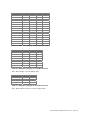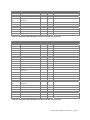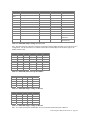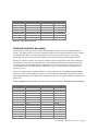
1
2030 Computer Manual
Revision 1.4
Copyright 1996 Digalog Systems Inc.
SYSTEM OVERVIEW .................................................................................................................................1
INSTALLATION ........................................................................................................................................2
RECEIVING INSPECTION .......................................................................................................................2
POWER REQUIREMENTS .......................................................................................................................3
ENVIRONMENTAL OPERATING CONDITIONS..................................................................................3
EXTERNAL CABLES AND CONNECTIONS .........................................................................................3
STARTUP ...................................................................................................................................................5
OPERATION ..............................................................................................................................................6
CHARACTER I/O DEVICES ...................................................................................................................9
MASS STORAGE PERIPHERALS...........................................................................................................9
G-96 MOTHER BOARD ASSEMBLY .....................................................................................................10
COMPUTER POWER SUPPLY SYSTEM ..............................................................................................13
GESMPU14-A MC68010 MICROPROCESSOR MODULE ..................................................................15
MEMORY CARD .......................................................................................................................................19
0000-2203, 0000-2213 ..............................................................................................................................20
0000-2232..................................................................................................................................................23
DUAL SERIAL PORT CARD ...................................................................................................................26
2000-3020 GESSIO-1B DUAL SERIAL PORT CARD ...................................................................................26
0000-3220, 0000-3520 DUAL SERIAL PORT CARDS...................................................................................32
SCSI/SASI HOST ADAPTER....................................................................................................................36
DISK CONTROLLER OMTI-5400...........................................................................................................39
I/O CONTROLLER ASSEMBLY .............................................................................................................42
SERIAL PORTS ............................................................................................................................................42
PRINTER PORT ............................................................................................................................................42
MEMORY MAP ...........................................................................................................................................42
I/O INTERFACE CARD ............................................................................................................................48
TESTHEAD CONTROLLER ASSEMBLY .............................................................................................49
GPIB CONTROLLER ASSEMBLY .........................................................................................................51
MASS STORAGE PERIPHERALS ..........................................................................................................56
HARD DRIVES ............................................................................................................................................56
FLOPPY DRIVE............................................................................................................................................56
MAINTENANCE ........................................................................................................................................57
PROCEDURE FOR INSTALLING 2ND HARD DISK............................................................................................57
TABLE 1 - 2030 MEMORY MAP ........................................................................................................................1
TABLE 2 - G96 INTERRUPT MAP ......................................................................................................................2
TABLE 3 - INTERRUPT MODES ..........................................................................................................................2
TABLE 4 - PERIPHERAL ADDRESSING MODES ..................................................................................................2
TABLE 5 - G96 MOTHER BOARD POWER SUPPY CONNECTOR PIN OUT ..........................................................10
TABLE 6 - G-96 BUS CONNECTOR PIN OUT ...................................................................................................11
TABLE 7 - DC POWER SUPPLY HARNESS CONNECTIONS ...............................................................................15
TABLE 8 - GESMPU14-A MEMORY MAP .....................................................................................................16
TABLE 9 - MK68901 TIMER INTERFACE CONNECTION ..................................................................................17
TABLE 10 - GESMPU14-A RS-232 CONNECTOR ..........................................................................................17
TABLE 11 - RESET/ABORT SWITCH CONNECTOR ...........................................................................................17
TABLE 12 - GESMPU-14A JUMPER SETTINGS FOR OS9 VERSION 2.4 ..........................................................18
TABLE 13 - 0000-2203 JUMPER SETTINGS, CAPACITY ...................................................................................20
TABLE 14 - 0000-2203 JUMPER SETTINGS, ADDRESS RANGE, FIRST EIGHT SETTINGS ..................................20
TABLE 15 - 0000-2213 JUMPER SETTINGS, CAPACITY ...................................................................................20
TABLE 16 - 0000-2213 JUMPER SETTINGS, ADDRESS RANGE, FIRST EIGHT SETTINGS ..................................21
TABLE 17 - 0000-2232 CARD TYPE SELECTION .............................................................................................23
TABLE 18 - 0000-2232 MEMORY SIZE SELECTION ........................................................................................23
TABLE 19 - 0000-2232 1 MEGABYTE CARD NUMBER SELECTIONS ...............................................................24
TABLE 20 - 0000-2232 2 MEGABYTE CARD NUMBER SELECTION .................................................................24
TABLE 21 - 0000-2232 4 MEGABYTE CARD NUMBER SELECTION .................................................................24
TABLE 22 - GESSIO-1B CHANNEL 1 ( /T5 ) CONNECTOR PIN OUT ..............................................................26
TABLE 23 - GESSIO-1B CHANNEL 2 ( /T6 ) CONNECTOR PIN OUT ...............................................................26
TABLE 24 - GESSIO-1B JUMPER SELECTIONS, OS-9 VERSION 2.4 ...............................................................30
TABLE 25 - 0000-3220, 0000-3520 CHANNEL 2 ( /T6 ) CONNECTOR PIN OUT .............................................32
TABLE 26 - 0000-3220, 0000-3520 CHANNEL 1 ( /T5 ) CONNECTOR PIN OUT ..............................................32
TABLE 27 - 0000-3220, 0000-3520 JUMPER SETTINGS FOR RS-232, OS9 VERSION 2.4 ................................33
TABLE 28 - 0000-3220, 0000-3520 JUMPER SETTINGS FOR RS-422, OS9 VERSION 2.4 ................................33
TABLE 29 - 2000-3022, 0000-3422 SCSI/SASI HOST ADAPTER MEMORY MAP...........................................36
TABLE 30 - 2000-3022 GESHDI-2A JUMPER SETTINGS FOR OS-9 VERSION 2.4 ..........................................36
TABLE 31 - 0000-3422 JUMPER SETTINGS FOR OS-9 VERSION 2.4 ................................................................38
TABLE 32 - 0000-1568 JUMPER SETTINGS FOR OS-9 V2.4 ............................................................................43
TABLE 33 - 0000-1568 OTHER INTERRUPT POSSIBILITIES .............................................................................43
TABLE 34 - 0000-2268 JUMPER SETTINGS FOR OS-9 V2.4 ............................................................................44
TABLE 35 - 0000-2268 OTHER INTERRUPT POSSIBILITIES .............................................................................44
TABLE 36 - 0000-1568 JUMPER SETTINGS FOR RS-232..................................................................................44
TABLE 37 - 0000-1568 JUMPER SETTINGS FOR RS-422..................................................................................44
TABLE 38 - 0000-2268 JUMPER SETTINGS FOR RS-232 .................................................................................45
TABLE 39 - 0000-2268 JUMPER SETTINGS FOR RS-422 .................................................................................45
TABLE 40 - 0000-1568, 0000-2268 OUTPUT CONNECTOR PIN OUT...............................................................45
TABLE 41 - /T1, /T2, /T3, /T4 CONNECTOR PIN OUT ......................................................................................48
TABLE 42 - /P CONNECTOR PIN OUT ..............................................................................................................48
TABLE 43 - /KP CONNECTOR PIN OUT ............................................................................................................49
TABLE 44 - 0000-2563 OUTPUT CONNECTOR PIN OUT ..................................................................................50
TABLE 45 - GPIB CONTROLLER ADDRESS MAP ............................................................................................51
TABLE 46 - 0000-1570 JUMPER SETTINGS FOR OS-9 V2.4 ............................................................................51
TABLE 47 - 0000-1570 OTHER INTERRUPT JUMPER POSSIBILITIES ................................................................52
TABLE 48 - 0000-1970 JUMPER SETTINGS FOR OS-9 V2.4 ............................................................................52
TABLE 49 - 0000-1970 OTHER INTERRUPT JUMPER POSSIBILITIES ................................................................52
TABLE 50 - 0000-1570, 0000-1970 J1 CONNECTOR PIN OUT ........................................................................53
TABLE 51 - 2000-3017 HARD DRIVE ADDRESS SELECTION ...........................................................................56
TABLE 52 - 2000-3016 FLOPPY DISK DRIVE JUMPER SETTINGS ....................................................................56
TABLE 53 - NEC D3142H /S2 JUMPER POSITIONS .......................................................................................57
TABLE 54 - TOSHIBA M222XD2 /S2 JUMPER POSITIONS...............................................................................57
System Overview
Control of the 2030 Series systems is based on the Motorola MC68010 microprocessor running Microware
Systems OS9 multitasking, multiple user operating system. This combination provides the ideal hardware and
software foundation for the real-time control and computing requirements of the 2030 systems. The back plane
used to communicate to the individual boards within the computer system is the Gespac G96 bus.
The standard computer system hardware configuration includes the MC68010 computer card, up to 8 M bytes
of SRAM memory, a SASI/SCSI interface, a 40 M byte hard disk, cartridge streamer tape drive, floppy disk
drive, and I/O controller card. The I/O controller card provides 4 serial ports, a printer port, and operator
keypad port. Optional cards for the computer system include a IEEE-488 controller and local area network
interface.
Digital test system emulator modules are interfaced to the computer system through the EMBus controller
board. The EMBus controller supports up to 6 emulator modules.
The TBus controller board provides the interface to the analog Testhead. The TBus controller maps a section
of the MC68010 memory for use by the boards of the Testhead. This is accomplished by extending the data
and address buses of the G96 bus through optically coupled buffers to the analog Testhead.
Start
$000000
$020000
$FBE900
$FBEA00
$FD0000
$FD0200
$FD0400
$FD0600
$FD8000
$FD8200
$FD8240
$FD8261
$FD8281
$FD82C2
$FE0000
End
$01FFFF
$FBE8FF
$FBE9FF
$FCFFFF
$FD01FF
$FD03FF
$FD05FF
$FD07FF
$FD81FF
$FD822F
$FD825F
$FD82C6
$FFFFFF
Description
RAM, overlaid by ROM after reset (128 K bytes)
Available for RAM
2030 analog Testhead
Available for RAM
peripheral block 0 (512 bytes)
peripheral block 1 (512 bytes)
peripheral block 2 (512 bytes)
peripheral block 3 (512 bytes)
X2212P 4 bit EEPROM (odd addresses only)
MK68901 peripheral (odd addresses only)
MM58274 calendar (odd addresses only)
write “1” to remove ROM from low RAM area
SMC8136 baud rate generator
NS16081 floating point coprocessor option
ROM
Table 1 - 2030 Memory Map
Board
Testhead Controller
MPU14A
Dual Serial Port Card
IRQ
7
(NMI)
6
5
Vector
31
Address
$FBE900
Device
/AMSint
I/O Mode
N/A (memory)
Vector Register
No (autovector)
74
$FD8201
Async.
Yes
76
$FD8201
Async.
Yes
70
$FD8201
Async.
Yes
71
$FD8241
Async.
Yes
77
$FD8201
Async.
Yes
29
$FD07F1
/term
(read)
/term
(write)
abort
button
real time
clock
tick
timer
/t5
Sync.
Yes (async mode)
2030 Computer Manual Revision 1.4 Page 1
Board
IRQ
I/O Controller
4
GPIB Controller
EVLAN-11
GESCNX
GESVIG
GESHDI
GESFDC-2B
EMBus Controller
4
3
3
?
1
1
Unused
Vector
29
80
80
81
81
82
82
82
83
65
67
??
25
25
Address
$FD07F5
$FD0001
$FD0011
$FD0021
$FD0031
$FD0041
$FD0041
$FD0041
$FD0101
$FD0400
$FD04C0
$FD0440
$FD0681
$FD0631
$FB8000
Device
/t6
/t1
/t2
/t3
/t4
/p
/opif
/kp
/g
/ev0
/kbd
/crt
/s0 - /s3
/f?
I/O Mode
Sync.
Async.
Async.
Async.
Async.
Async.
Async.
Async.
Async.
Async.
Async.
Async.
Sync.
Sync.
N/A (memory)
Vector Register
Yes (async mode)
Yes
Yes
Yes
Yes
Yes
Yes
Yes
Yes
Yes
Yes
Yes
No (autovector)
No (autovector)
No (autovector)
Table 2 - G96 Interrupt Map
Notes for G96 Interrupt Map:
1. The polarity of IACK is active HIGH which follows the G64 convention.
2. Synchronous devices are autovectored.
IRQ Number
1
2
3
4
5
6
7
Mode
Autovectored
Undefined
Vectored
Vectored
Autovectored
Vectored (only used by the MPU14A board)
Autovectored
Table 3 - Interrupt Modes
Address Range
$FD0000-$FD01FF
$FD0200-$FD03FF
$FD0400-$FD05FF
$FD0600-$FD07FF
Mode
Asynchronous
Asynchronous
Asynchronous
Synchronous
Table 4 - Peripheral Addressing Modes
INSTALLATION
This section contains information regarding the shipment, inspection, installation and self test of the Series
2030 CPU. The Series 2030 CPU is shipped essentially ready for use when received. However, the following
sections should be covered before attempting to operate the system.
RECEIVING INSPECTION
A close visual inspection should be performed promptly after the system has been received. Any evidence of
rough handling should be reported to the shipper and to Digalog Systems.
Look for broken switches, scratched or dented panel surfaces, and for any other damage to the exterior of the
unit. Also check the Terminal and cables for possible mishandling. If damages of any kind are found, refer to
the procedures outlined in the warranty at the beginning of this manual.
2030 Computer Manual Revision 1.4 Page 2
The Emulator is shipped fully operational apart from the systems connections which must be made in
accordance with Section 3.13. However, a careful inspection should be performed to ensure functionality.
POWER REQUIREMENTS
The Series 2030 CPU requires 115 VAC. A standard power cord is included. Care must be taken to ensure that
the unit is grounded properly. If grounding outlets are not available, adapters with grounding connections must
be used.
ENVIRONMENTAL OPERATING CONDITIONS
The Series 2030 CPU is designed for use between 10 and 40 degrees Celsius. A cooling fan is mounted on the
front panel of the unit to provide cooling for the system's electronics. Care must be taken to ensure that fan
openings remain uncovered for proper air flow.
DAMAGE may occur if the filters are not periodically cleaned.
EXTERNAL CABLES AND CONNECTIONS
Depending on the system configuration, cable connections will need to be made between some or all of the
following devices: Computer, Terminal, Printer, Keypad, Testhead, Emulator and GPIB Instruments.
2030 Computer Manual Revision 1.4 Page 3
Power inlet
/T1 serial port
/T2 serial port
/T3 serial port
/TERM serial
port
/T4 serial port
/P printer port
GPIB
connector
/KP keypad
port
TBus connector
Figure 1 - 2030 Computer Back Panel
2030 Computer Manual Revision 1.4 Page 4
STARTUP
Ordinarily, when power is applied or the reset button is released, the loader program will bring up the
OS9/68000 operating system from the hard disk, and the system will begin accepting commands from the
console keyboard (or will request a user to log in). It may be instructive to see exactly what happens during this
complicated process to help users diagnose (and avoid) problems and make the most of the many opportunities
to fine-tune the operating system to their personal requirements.
The loader is located in EPROM on the CPU board at $FE0000-$FFFFFF. When the RESET line is asserted by
the power-on reset circuit, reset push-button, or reset instruction, the memory map is switched to overlay the
EPROMs at $000000-$01FFFF. The microprocessor enters supervisor state, loads its stack pointer from
locations 0-3, and loads its program counter from locations 4-7. The loader is executed and immediately clears
a latch to restore RAM access at $0000000-$01FFFF.
The loader then begins to initialize RAM. All of the 68010 exception vectors at $000C- $03FF (all vectors
except reset and bus error, which are handled in the EPROMs) are assigned values starting at $00000040A and
incremented by 10. In turn, between $040A and $0DEB, a 10-byte routine is installed for each vector. These
short routines consist of the instructions PEA #xxxx, JMP yyyyyyyy. (The reason for having the original
vectors essentially point to jump instructions is to allow implementing OS9 on hardware which does not permit
the original vectors to be in RAM. The jump instructions provide a second level of vectors which will always
be in RAM and thus dynamically configurable by the operating system.) The loader does not need to initialize
the jump addresses. That is done later by the OS9 kernel using its own F$IRQ service request. The PEA
arguments start at $000C and increment by 4 and thus are equal to the original vector offsets. (The 68010
automatically stacks the vector offset, but OS9 was designed for the 68000, which did not.)
The loader then determines the amount of RAM in the system and creates a linked list of RAM blocks. OS9
was designed to work with noncontiguous memory blocks, but our loader only recognizes the contiguous block
starting at location 0, so the linked list is trivial.
This is when the message, "DIGALOG SYSTEMS, INC." is displayed. The loader requests the SASI interface
to read logical sector number zero of logical unit number zero (the hard disk). OS9 disks contain the boot file
location in bytes $15-$17 of this sector and the boot file size in bytes $18-$19. If the size word is nonzero, a
seek is performed to the indicated sector and the file is loaded into RAM starting at $2400. The loader then
transfers control to the module at $2400 (which should be the OS9 kernel). At this point, the loader is finished.
The loader may not be able to find the boot file on logical unit zero. This always occurs on the first few
attempts after a cold start while the hard disk is not yet up to speed. The loader would then try unit one (floppy
disk) starting over from where the DIGALOG SYSTEMS message is displayed. As long as a boot file cannot
be located on either unit, the loader will alternate between units trying to locate one.
The loader can be directed to get the boot file from the hard disk by removing the floppy disk before powering
up the computer or resetting the CPU. The loader can be forced to get the boot file from a floppy disk by
turning off the power briefly, thus causing the hard disk to lose enough speed whereby the floppy drive is
accessed first. In either case, the desired unit must contain a valid boot file. Boot files are installed with the
utility program OS9GEN, which makes the file contiguous and installs the size and location in sector zero as
mentioned above. The boot file (OS9Boot) is made up of modules; some are mandatory and others, optional.
KERNEL must be the first module. The others may be in any order. INIT is mandatory; it is a data module
containing system configuration parameters (see the OS9/68000 technical manual for a description of the INIT
module).
RBF is required for any disk I/O; GESHDI is required to operate the SASI controller and S0 & RB5400 are
needed for the hard disk and floppy disk units. SYSGO is required; it is a simple endless loop, which is
actually the mainline program of the entire operating system. The boot file is limited to 64K bytes, which
requires some of the necessary modules to be located in the boot loader EEPROM. When the KERNEL starts,
2030 Computer Manual Revision 1.4 Page 5
it will search memory for modules and add any it finds to the module directory. The following modules are
located in the boot loader EEPROM: SHELL, which is the command line interpreter; CLOCK and TK68901,
which implement the real time clock; and MK68901, which is the console serial port driver. The descriptor
TERM, which is for the console serial port, is located in the boot file to allow its characteristics (such as baud
rate) to be changed. Any other modules that are desired may be loaded later. When control is passed to the
kernel, it initializes the operating system tables and data structures and then transfers control to SYSGO. In
turn, this transfers control to the command line interpreter, SHELL. This is more complicated than absolutely
necessary, but it makes OS9 adaptable to a wider variety of applications.
The shell is capable of reading command lines from the disk as well as from the terminal. The file
/S0/STARTUP is passed by SYSGO to the shell as its first set of commands. This is where most system
customization takes place. The clock is set (from the battery powered calendar), additional I/O modules are
loaded, terminal port parameters are adjusted, time sharing consoles are activated, the message of the day is
displayed, etc. In short, any command can be given to or any program can be run by STARTUP. If and when
these commands have all been executed, the shell then takes input from the console. Time-sharing consoles
e.g., /T1, may be activated by the command:
SHELL </T1 >/Tl >>/T1&
which will not require a login password. However, if the user leaves the shell by typing
control-Z, no additional login sessions are possible. Usually, these consoles are activated with the command:
TSMON /T1 &
which uses CMDS/LOGIN and SYS/PASSWORD to request the user's ID. If the user leaves the shell, future
login sessions are still possible.
References: OS9/68000 user manual sections. 1, 2, 3.3, 5; OS9GEN, TSMON commands; technical manual
sections 1.1, 2, 5.1. For creating text files, such as Startup, see BUILD and EDT commands or SCRED screen
editor user's manual.
OPERATION
Microware’sOS9/68000 operating system is an advanced multitasking operating system designed for high
performance in real-time system applications. It combines significant new operating system concepts with the
overall architecture of Unix; yet OS9/68000 is by far smaller and more efficient than Unix. OS9/68000
supports modular programming techniques that multiply programmer efficiency and dramatically improve
software maintainability. Its tree-structured directory system and memory module format allow dynamic
linking of standard library or custom modules together to form an overall application program.
Microware’s BASIC combines all the standard BASIC statements with advanced features, such as PASCALtype loop constructs and data structures. It is procedure oriented, supports modular programming, and is totally
integrated into the OS9 modular software environment. Procedures may call each other (or themselves)even
using automatic parameter passing. External procedures written in Basic09, C, or assembly language can be
mixed freely and interchangeably.
Most of the system utilities that are available through the Shell (console command interpreter) are described in
the Microware OS9/68000 User's Guide. This manual also describes the Shell itself and the OS9 file system.
Many of the same language or equivalent utilities are accessible in assembly language through system service
requests (using a trap instruction). These calls are described in the OS9/68000 Technical Manual. This manual
is also useful to advanced Basic09 programmers who need detailed knowledge of the I/O system, memory
management, and process scheduling.
Microware BASIC has its own manual. The section describing external procedure calls (the RUN statement) is
of interest not only to users who write their own assembly language procedures, but also to anyone desiring
more insight into the nature of the Digalog extensions to Basic09 which interface with the test system
2030 Computer Manual Revision 1.4 Page 6
hardware. Finally, the Relocating Macro Assembler (R68/L68) and screen editor (UMacs) are described in
their own separate manuals ( a lower performance text editor, Edt, is described as a utility in the user's
manual). Although Microwave BASIC has its own interactive source text editor, it is possible to write source
programs using UMacs. UMacs can also used to write and maintain the Startup file (and any other user
command files), Sys/Password file (used by Login), assembly language source files, etc.
2030 Computer Manual Revision 1.4 Page 7
Reset switch.
Floppy disk
drive (/S1)
Tape drive
(/mt0, /s3)
Figure 2 - 2030 Computer Front View
2030 Computer Manual Revision 1.4 Page 8
CHARACTER I/O DEVICES
The standard character I/O devices are of four types: asynchronous bit-serial ports for terminals and modems, a
parallel Centronix type port for printers, a parallel IEEE-488 (GPIB) port for instruments, and a port for the
small 24-key pad.
Serial port /TERM is physically located on the CPU board and serves the main (or only) user console.
Serial port /T1, /T2, /T3 and /T4 are located on the I/O controller board and are for additional user terminals or
any other purpose such as serial printers, data networks, bar-code readers, etc.
All ports /TERM and /T1-/T4 conform to EIA-RS232 pinout and signal levels. Baud rate, character format, and
other operating characteristics are determined by the XMODE utility program.
The parallel port /P implements a subset of the Centronix interface (8 data, strobe, and acknowledge) and is
compatible with most printers. The XMODE utility may be used to set a time limit for acknowledge.
The IEEE-488 port, /G, is described in a separate section (4.11).
The keypad may be used two ways. As a standard OS9 I/O device (/KP), it provides a subset of the ASCII
character set including the digits 0-9, symbols +.-/*&$ etc., letters a- h and A-H, delete, cancel, and carriage
return. Alternatively, the procedure KPscan(N) reads the instantaneous state of the keypad as a key number 023 (24 for no key). This permits the keypad to be polled at any time for the duration of a keystroke to be
determined as well as its identity.
MASS STORAGE PERIPHERALS
Four devices are used for file storage and backup: the hard disk (/S0), floppy (/S1), streaming back-up tape
(/S3) and incremental tape backup (/mt0). A SASI interface controller is used.
The standard hard disk is a four-surface plated media design with a formatted capacity of 40 Mb (1 Mb =
1048576 bytes). However, other drives of similar capacity may be substituted as availability changes.
The floppy disk format is double sided, double bit density, double track density (96 TPI, 80 tracks) for a
formatted capacity of 655360 bytes.
The back-up (streaming) tape uses the QIC-02 format with a high-capacity cassette style cartridge. The hard
disk may be backed up and restored as a whole disk image for emergency use. The back-up tape may be used
as a (very slow) read only device for recovery of individual files by treating the tape drive as a disk. The file
descriptor used for this is s3. For individual file or directory backup, the user may execute the Fsave and
Frestore commands. The descriptor used for doing this is /mt0. Follow the Fsave/Frestore instructions found in
the Microware manual sets. Because of the way Fsave writes files to the tape, incremental restoration of files is
much faster than trying to restore them from a streamed (bit image) tape.
The floppy disk cannot be backed up to or used as a hard disk back-up per se other than that individual files
may be read or written in the usual manner. In particular, the OS9 BACKUP command is not used with this
system. The DSAVE command may be used in conjunction with the COPY command to copy all files on a
device or in a subdirectory. DSAVE produces a shell procedure file which may be viewed and edited before
execution to copy a particular list of files to a target device for backup purposes.
For backing up the hard disk, the command BSTREAM may be used. This will display the tape ID block (if
the tape has been used previously) and prompt for an R (restore) or B (back-up) command. Bstream is limited
to backing up 40Mb (or less) hard disks as it does not support multiple volume backups. An alternative way of
backing up the system's hard disk is to use the Fsave command. This program does a file-by-file backup of the
hard disk structure and files and supports multiple volumes (tapes) if a hard drive larger than 40 MB needs to
be backed up. Fsave uses the descriptor /mt0. Other tape operations may be accessed through the tape utility
2030 Computer Manual Revision 1.4 Page 9
provided by Microware. They include erasing, rewinding, reading and writing tapes. Please refer to the
Microware manual set for more information on the tape utility.
When the equipment is to be moved, stored, or transported, it is recommended to park the hard disk heads on a
reserved landing zone of the disk surface. The command BPARK is used for this purpose.
Before a new hard disk or floppy can be used, it must be formatted, which provides it with sector address
marks and a blank directory structure. In addition, if a device is to be used as the source of the boot file (see
this manual section 3.14), the OS9GEN command must be used to properly initialize it.
References: OS9/68000 user manual ATTR, COPY, DEL, DELDIR, DIR, DSAVE, FORMAT, FREE,
MAKDIR, OS9GEN and RENAME commands; chapter 4 (the OS9 file system).
G-96 Mother board Assembly
The G-96 bus offers 8 and 16 bit data bus capability, synchronous and asynchronous data transfers, single Euro
board mechanical standard and a high reliability DIN 41612 connector. Twenty-four address lines and a signal
named PAGE* allow a 32M word (64M bytes) address space. The GESMPU14-A computer card (Digalog
P.N. 2025-1020) can access up to 16M bytes.
The interrupt structure includes 6 interrupt lines, 1 interrupt acknowledge, and a daisy chain implementation
that allows both vectored and non-vectored interrupts to be used at the same time.
The G96 bus must be terminated at one end with 3 volt@132 ohm resistor networks. These networks are
included on the EMBus controller card (Digalog P.N. 0000-2211). If the system is an analog test system, the
termination is provided by a terminator card (Digalog P.N. 0000-2007). Terminators are located in the far
right hand slot. Only the power lines and interrupt daisy chain lines are without terminators.
VPA* (valid peripheral address) is the address strobe for the peripheral area. VMA* is used for all other
address validation. VPA*, VMA* and IACK* are mutually exclusive.
Address lines A0-A23 refer to word addresses with UDS* and LDS* selecting even or odd byte addresses.
Thus, A1 on the MC68010 is connected to A0 on the G-96 bus, A2 to A1, A3 to A2, etc. A23 of the G96 bus
is driven low and is unused by the GESMPU14-A board.
For further information, refer to the “G-64 Bus Specifications Manual,” Revision 3.0, June 1988.
Pin Number
1
2
3
4
5
6
7
Power Supply
-12V
+5V STANDBY
+12V
+5V
+5V
GND
GND
Table 5 - G96 Mother board Power Suppy Connector Pin Out
2030 Computer Manual Revision 1.4 Page 10
PIN
C1
C2
C3
C4
C5
C6
C7
C8
C9
C10
C11
C12
C13
C14
C15
C16
C17
C18
C19
C20
C21
C22
C23
C24
C25
C26
C27
C28
C29
C30
C31
C32
SIGNAL
GND
A16
A17
A18
A19
A20
A21
A22
A23
GND
IRQ3*
IRQ5*
VED* (NC)
GND
P5* (NC)
P4* (NC)
P3* (NC)
P2* (NC)
P1* (NC)
P0* (NC)
SYSFAIL* (NC)
ARBCLK (16 MHz)
+5V
GND
PIN
B1
B2
B3
B4
B5
B6
B7
B8
B9
B10
B11
B12
B13
B14
B15
B16
B17
B18
B19
B20
B21
B22
B23
B24
B25
B26
B27
B28
B29
B30
B31
B32
SIGNAL
GND
A8
A9
A10
A11
A12
A13
A14
A15
BRQ*
UDS*
BGACK*
E
RESET*
NMI*
IRQ1*
IRQ2*
IACK*
D12*
D13*
D14*
D15*
D4*
D5*
D6*
D7*
BERR*
CHAIN IN
+5 STANDBY
-12V
+5V
GND
PIN
A1
A2
A3
A4
A5
A6
A7
A8
A9
A10
A11
A12
A13
A14
A15
A16
A17
A18
A19
A20
A21
A22
A23
A24
A25
A26
A27
A28
A29
A30
A31
A32
SIGNAL
GND
A0
A1
A2
A3
A4
A5
A6
A7
BGRT*
LDS*
HALT*
SYCLK (8 MHz)
VPA*
DTACK*
VMA*
R/W*
IRQ4*
D8*
D9*
D10*
D11*
D0*
D1*
D2*
D3*
PAGE*
CHAIN OUT
PWF*
+12V
+5V
GND
Table 6 - G-96 Bus Connector Pin Out
2030 Computer Manual Revision 1.4 Page 11
Figure 3 - 0000-2230 G96 Mother Board
2030 Computer Manual Revision 1.4 Page 12
Computer Power Supply System
The 2030 computer chassis is powered from one power supply with multiple outputs. This power supply
provides +5 volts, -12 volts and 2 separate +12 volt supplies. 115V AC power (50/60 Hz) is provided to the
supply via a combination power entry module, fuse holder and line filter. The entry fuse is a 3 amp slow blow
fuse.
2030 Computer Manual Revision 1.4 Page 13
Figure 4 - 0000-2067 AC Power Supply Harness Installation
2030 Computer Manual Revision 1.4 Page 14
Power Supply Pin
Number
1
2
3
4
5
6
7
8
9
+S
-S
Signal
Description
+5 volts
+5 volts
GND
GND
+12 volts
GND
+12 volts
-12 volts
Unused
+5 volt sense line
GND sense line
G-96 Mother board Pin
Number
4,5
Hard disk Pin Number
4
6,7
3
1
2
3
1
4
6
Table 7 - DC Power Supply Harness Connections
Note: Below is pictured a hard disk connector on the DC harness.
4
3
2
1
GESMPU14-A MC68010 Microprocessor Module
The GESMPU14-A is a high performance computer board based on the MC68010 32 bit microprocessor. It
includes a battery powered calendar/clock, asynchronous serial port, sockets for up to 128K bytes of PROM, a
small EEPROM with 256 4 bit words, and a socket for an optional NS16081 arithmetic co-processor.
The MK68901 multifunction peripheral provides the serial port, four user programmable timers, and interrupt
vectoring for the other on board functions.
The EPROMs provide boot strap software that loads the OS-9 operating system from the SASI disk controller.
They also contain a monitor for bus error and abort push-button exceptions.
The MC68010 microprocessor requires a DTACK* signal (data transfer acknowledge) to complete each
address cycle. On this board, an 8 microsecond timer will generate a bus error if the DTACK* signal does not
occur within this time. The faulted cycle will be rerun up to 8 times automatically by on board logic before the
MC68010 is allowed to fetch the bus error vector and initiate an exception. Each retry is preceded by a 100
millisecond delay making the systems very robust in surviving power transients. Once the bus error exception
is initiated, the system will enter the bus error monitor. It is advised that the user write down the information
displayed on the screen so that the information is available later while debugging the system. A hardware reset
is usually the only method that can be used to recover from this error condition.
2030 Computer Manual Revision 1.4 Page 15
The system clock rate is 8 MHz. A machine cycle requires at least 4 clock cycles (8 states). With static RAM,
the CPU can maintain 16 bit memory transfers at 2 MHz.
INT1* through INT5* are assigned hardware interrupt levels 1-5, which may be vectored or autovectored.
Level 6 is always vectored by the MK68901, which handles the serial port, abort button, and PWF* (power
fail) interrupts. NMI* (nonmaskable interrupt) is connected at level 7 and is always autovectored.
On board logic decodes a 2K byte block of addresses for peripherals. Address locations in this area use the
address qualifier VPA*. Within this 2K byte block, 4 blocks of 512 bytes may be individually jumpered for
either asynchronous transfer using DTACK* or synchronous transfer using the 1 MHz E clock.
When the computer board is reset, the on board EPROM will overlay the lowest block of memory addresses
(including the vector table) as well as appear at the EPROM addresses. During system initialization, the
software will set an on board latch to remove the EPROM from the low addresses and permit access to RAM
instead.
There are three LEDs on the front edge of the board. The red indicates the supervisory mode (from the
MC68010 function code). The yellow indicates a bus error retry. The green indicates a microprocessor halt.
Only a hardware reset will restart a halted microprocessor.
The yellow LED will also light during a synchronous data transfer. When the bus timer does time out and
lights the LED, the MC68010 ignores the BERR* signal during the asynchronous transfer.
Start
$000000
$020000
$FBE900
$FBEA00
$FD0000
$FD0200
$FD0400
$FD0600
$FD8000
$FD8200
$FD8240
$FD8261
$FD8281
$FD82C2
$FE0000
End
$01FFFF
$FBE8FF
$FBE9FF
$FCFFFF
$FD01FF
$FD03FF
$FD05FF
$FD07FF
$FD81FF
$FD822F
$FD825F
$FD82C6
$FFFFFF
Description
RAM: overlaid by ROM after reset (128K bytes)
Available for RAM
2030 analog Testhead
Available for RAM
Peripheral Block 0 (512 bytes)
Peripheral Block 1 (512 bytes)
Peripheral Block 2 (512 bytes)
Peripheral Block 3 (512 bytes)
X2212P 4-bit EEPROM (odd addresses only)
MK68901 peripheral (odd addresses only)
MM58274 calendar (odd addresses only)
Write “1” to remove ROM from low RAM area
SMC8136 baud-rate generator
NS16081 floating-point coprocessor option
ROM
Table 8 - GESMPU14-A Memory Map
For pin assignments of the G-96 bus connector, please see the section titled “G-96 Mother board Assembly”.
Connector - Pin
P2-1
P2-2
P2-3
P2-4
P2-5
P2-6
P2-7
P2-8
P2-9
P2-10
Signal
Gate 0
Output 0
GND
Gate 1
Output 1
GND
Output 2
GND
Output 3
GND
2030 Computer Manual Revision 1.4 Page 16
Table 9 - MK68901 Timer Interface Connection
Note: The above connector is normally not used as part of the 2030 tester configuration.
Connector - Pin
P4-1
P4-3
P4-5
P4-7
P4-9
P4-11
P4-13
P4-15
P4-17
P4-19
Signal
Shield
RxD
CTS
GND
TxClock
RxClock
Connector - Pin
P4-2
P4-4
P4-6
P4-8
P4-10
P4-12
P4-14
P4-16
P4-18
P4-20
Signal
TxD
RTS
DSR
DCD
DTR
Table 10 - GESMPU14-A RS-232 Connector
Connector-Pin
P3-1
P3-2
P3-3
P3-4
P3-5
Signal
Reset switch
GND
Abort switch N.C.
Abort switch N.O.
+5 volts
Table 11 - Reset/Abort Switch Connector
Note: J1 jumper must be open for external use of the abort switch.
Note that when setting the jumpers on most Gespac cards, the jumper field is numbered like most integrated
circuits i.e., in a U-shaped pattern.. For further reference, consult the GESMPU-14A data sheet.
Jumper
Field
J1
J2
Function
Jumpers
Settings
Result
Local/Remote abort selector
Internal/External Tx and Rx clock
selector
J1-1 to J1-2
J2-1 to J2-10
Closed
Closed
Local abort switch
Internal baud rate
clock
J2-2 to J2-3
J2-8 to J2-9
J2-4 to J2-7
J2-5 to J2-6
J4-1 to J4-18
J4-2 to J4-17
J4-3 to J4-16
J4-4 to J4-15
J4-5 to J4-14
J4-6 to J4-13
J4-7 to J4-12
J4-8 to J4-11
J4-9 to J4-10
J5-1 to J5-10
Closed
Closed
Open
Open
Open
Open
Closed
Closed
Closed
Closed
Closed
Closed
Closed
Open
J5-2 to J5-9
J5-3 to J5-8
Open
Closed
J4
RS-232C modem/terminal selector
J5
EPROM access time selector, bus
system clock selector
DCE (modem)
450 ns access time,
8 MHz system
clock
2030 Computer Manual Revision 1.4 Page 17
Jumper
Field
J6
J7
Function
Real time clock power enable
Async/Sync VPA field mode,
Autovectored/vectored interrupt
selector
J8
IACK sense selection
J9
EPROM type selection
J10
EPROM type selection
J11
SYCLK and Enable three state
control, IACK three state control,
power fail signal selector
Note
Jumpers
Settings
Result
J5-4 to J5-7
J5-5 to J5-6
J6-1 to J6-2
J7-1 to J7-18
Closed
Open
Closed
Open
Battery connected
VPA field 0 async.
J7-2 to J7-17
J7-3 to J7-16
J7-4 to J7-15
J7-5 to J7-14
J7-6 to J7-13
J7-7 to J7-12
J7-8 to J7-11
J7-9 to J7-10
J8-1 to J8-2
J8-2 to J8-3
J9-1 to J9-2
J9-2 to J9-3
J10-1 to J10-2
J10-2 to J10-3
J10-4 to J10-5
J10-5 to J10-6
J11-1 to J11-2
Open
Open
Closed
Open
Closed
Closed
Open
Open
Closed
Open
Closed
Open
Open
Closed
Closed
Open
Open
J11-2 to J11-3
J11-4 to J11-5
Closed
Open
J11-5 to J11-6
J11-7 to J11-8
Closed
Open
VPA field 1 async.
VPA field 2 async.
VPA field 3 sync.
IRQ5 autovectored
IRQ4 vectored
IRQ3 vectored
IRQ2 autovectored
IRQ1 autovectored
IACK when high
27256
27256
IACK active during
DMA
Enable, SYCLK
free running during
DMA
No power fail
interrupt
Jumper field J3 does not exist.
Table 12 - GESMPU-14A Jumper Settings for OS9 Version 2.4
2030 Computer Manual Revision 1.4 Page 18
Figure 5 - 2025-1020 GESMPU-14A Computer Card
Memory Card
Three different memory cards are used in the 2030 computer systems. The first two use the same printed
circuit board. The 256 kilobyte board uses 32 8 kilobyte SRAM chips and has the Digalog P.N. 0000-2203.
The 1 megabyte board uses 32 kilo byte SRAM chips and has the Digalog P.N. 0000-2213. The only way to
tell the two cards apart is to identify the type of chip on the board. The 1 megabyte configuration is the most
popular.
2030 Computer Manual Revision 1.4 Page 19
The last memory card used in the 2030 computer is the 0000-2232 card. While this card may be configured up
to 6 ways, only one has been used. This configuration is the 1 megabyte configuration.
0000-2203, 0000-2213
This is a no wait state static RAM board using 32 8 bit memory chips surface mounted on one side of the card.
When equipped with 8 kilo byte chips the total capacity is 256 kilo bytes. When equipped with 32 kilo byte
chips the capacity is 1 megabyte per board. In any system which contains both 256 kilobyte and 1 megabyte
memory boards, the 1 megabyte boards must be addressed first, followed by the 256 kilobyte boards.
Jumper Field
JP8
Function
Board capacity
JP9
Board capacity
JP10
Board capacity
JP11
Board capacity
JP13
JP14
Board capacity
Board capacity
Jumpers
A to B
B to C
A to B
B to C
A to B
B to C
A to B
B to C
1 to 2
1 to 2
Settings
Closed
Open
Closed
Open
Closed
Open
Closed
Open
Closed
Closed
Result
256 kilo byte
256 kilo byte
256 kilo byte
256 kilo byte
256 kilo byte
256 kilo byte
Table 13 - 0000-2203 Jumper Settings, Capacity
Address Range
$00000000 - $0003FFFF
$00040000 - $0007FFFF
$00080000 - $000BFFFF
$000C0000 - $000FFFFF
$00100000 - $0013FFFF
$00140000 - $0017FFFF
$00180000 - $001BFFFF
$001C0000 - $001FFFFF
JP7
Closed
Closed
Closed
Closed
Closed
Closed
Closed
Closed
JP6
Closed
Closed
Closed
Closed
Closed
Closed
Closed
Closed
JP5
Closed
Closed
Closed
Closed
Closed
Closed
Closed
Closed
JP4
Closed
Closed
Closed
Closed
Closed
Closed
Closed
Closed
JP3
Closed
Closed
Closed
Closed
Open
Open
Open
Open
JP2
Closed
Closed
Open
Open
Closed
Closed
Open
Open
JP1
Closed
Open
Closed
Open
Closed
Open
Closed
Open
Table 14 - 0000-2203 Jumper Settings, Address Range, First Eight Settings
Jumper Field
JP8
Function
Board capacity
JP9
Board capacity
JP10
Board capacity
JP11
Board capacity
JP13
JP14
Board capacity
Board capacity
Jumpers
A to B
B to C
A to B
B to C
A to B
B to C
A to B
B to C
1 to 2
1 to 2
Settings
Open
Closed
Open
Closed
Open
Closed
Open
Closed
Open
Open
Result
1 megabyte
1 megabyte
1 megabyte
1 megabyte
1 megabyte
1 megabyte
Table 15 - 0000-2213 Jumper Settings, Capacity
2030 Computer Manual Revision 1.4 Page 20
Address Range
$00000000 - $000FFFFF
$00100000 - $001FFFFF
$00200000 - $002FFFFF
$00300000 - $003FFFFF
$00400000 - $004FFFFF
$00500000 - $005FFFFF
$00600000 - $006FFFFF
$00700000 - $007FFFFF
JP7
Closed
Closed
Closed
Closed
Closed
Closed
Closed
Closed
JP6
Closed
Closed
Closed
Closed
Closed
Closed
Closed
Closed
JP5
Closed
Closed
Closed
Closed
Open
Open
Open
Open
JP4
Closed
Closed
Open
Open
Closed
Closed
Open
Open
JP3
Closed
Open
Closed
Open
Closed
Open
Closed
Open
JP2
Open
Open
Open
Open
Open
Open
Open
Open
JP1
Open
Open
Open
Open
Open
Open
Open
Open
Table 16 - 0000-2213 Jumper Settings, Address Range, First Eight Settings
2030 Computer Manual Revision 1.4 Page 21
Figure 6 - 0000-2203/0000-2213 Memory Card
For pin assignments of the G-96 bus connector, please see the section titled “G-96 Mother board Assembly”.
2030 Computer Manual Revision 1.4 Page 22
0000-2232
This G64/G96 form factor card allows the system to have 1, 2 or 4 megabytes of no wait state static RAM. It
can also be configured for 1, 2 or 4 megabytes of PROM. The card accepts either 128 kilo byte SRAM or
PROM chips, for the 1 megabyte mode, or 512 kilo byte SRAM or PROM chips for the 2 or 4 megabyte
modes.
In the 2 megabyte mode the sockets for the SRAM/PROM are half populated. 512 kilo byte chips are placed in
U1, U3, U5 and U7.
In any of the selected configurations the address lines are routed through a PLD such that no gaps appear in the
memory map. When using the selection jumpers, the user selects a card number. To translate the card number
into the base address, multiply the card number by the memory capacity of the card. When using the selection
jumpers on the card it should be remembered that you are selecting the card number. To translate the card
number to the base address multiply the card number times the memory capacity of the card. Examples:
Card number 0, 4 megabyte capacity: $000000 * $400000= $000000
Card number 1, 4 megabyte capacity: $000001 * $400000= $400000
Card number 3, 1 megabyte capacity: $000003 * $100000= $300000
When placing memory cards of mixed capacity in the same system the following practice is recommended.
Place the largest capacity card (e.g. 4 megabyte ) lowest in the memory map (i.e. $000000). Place the next
largest capacity card in the memory map following the last address of the first card. Continue placing
successively lower capacity cards in the system with addresses following the previous card. An example
follows:
Card Number
0
2
6
Size
4 megabyte
2 megabyte
1 megabyte
Address Range
$000000 - $3FFFFF
$400000 - $5FFFFF
$600000 - $7FFFFF
Note that even though there are not six 1 megabyte cards in the system, the 1 megabyte card had to be selected
as card number six to get base address $600000.
The physical location of the cards in the rack are irrelevant with the exception of the chain-in and chain-out
jumper. This jumper is used to connect or separate cards on the same interrupt vector.
Jumpers
JP1
JP8
Function
Memory type, ROM or
RAM
Chain-in Chain-out
Jumper
JP1
Setting
Open
Result
Card selected for RAM
JP8
Open
Chain-in not connected to chain-out
Table 17 - 0000-2232 Card Type Selection
Memory Size
Forbidden Condition
1 megabyte
2 megabyte
4 megabyte
JP2
Closed
Open
Closed
Open
JP3
Closed
Closed
Open
Open
Table 18 - 0000-2232 Memory Size Selection
2030 Computer Manual Revision 1.4 Page 23
Card Number
0
1
2
3
4
5
6
7
8
9
A
B
C
D
E
F
JP4
Closed
Open
Closed
Open
Closed
Open
Closed
Open
Closed
Open
Closed
Open
Closed
Open
Closed
Open
JP5
Closed
Closed
Open
Open
Closed
Closed
Open
Open
Closed
Closed
Open
Open
Closed
Closed
Open
Open
JP6
Closed
Closed
Closed
Closed
Open
Open
Open
Open
Closed
Closed
Closed
Closed
Open
Open
Open
Open
JP7
Closed
Closed
Closed
Closed
Closed
Closed
Closed
Closed
Open
Open
Open
Open
Open
Open
Open
Open
Table 19 - 0000-2232 1 Megabyte Card Number Selections
Card Number
0
1
2
3
4
5
6
7
JP5
Closed
Open
Closed
Open
Closed
Open
Closed
Open
JP6
Closed
Closed
Open
Open
Closed
Closed
Open
Open
JP7
Closed
Closed
Closed
Closed
Open
Open
Open
Open
Table 20 - 0000-2232 2 Megabyte Card Number Selection
Note: JP4 is unused. Leave the jumper open.
Card Number
0
1
2
3
JP6
Closed
Open
Closed
Open
JP7
Closed
Closed
Open
Open
Table 21 - 0000-2232 4 Megabyte Card Number Selection
Note: JP4 and JP5 are not used. Leave the jumpers open.
2030 Computer Manual Revision 1.4 Page 24
Figure 7 - 0000-2232 Memory Card
For pin assignments of the G-96 bus connector, please see the section titled “G-96 Mother board Assembly”.
2030 Computer Manual Revision 1.4 Page 25
Dual Serial Port Card
The Dual Serial Port Card provides two serial communication channels on the G64/G96 bus. As configured
for use in the Digalog Systems computer, the card offers asynchronous communication using the RS-232C
protocol. Its baud rate is software programmable. RS-422 levels are also possible with this card. The TTY
interface on the GESSIO cards is not supported by Digalog Systems.
The communication ports on this card are known to the operating system through the device descriptors “t5”
and “t6.” The settings of each device descriptor as shipped from Digalog are listed in the back of this manual.
The device driver “sc6850” and the file manager “SCF” are used to control the card.
Four different Dual Serial Port Cards are in use on the 2030 computers. They are the GESSIO-1A and
GESSIO-1B cards (Digalog P.N. 2000-3020) and Digalog’s Dual Serial Port Card (P.N. 0000-3220 and 00003520). All cards except the GESSIO-1A are interchangeable without having to change the software. The
GESSIO-1A card cannot be used with the Digalog implementation of the OS-9 operating system, version 2.4
and above.
2000-3020 GESSIO-1B Dual Serial Port Card
Connector - Pin
P2-1
P2-3
P2-5
P2-7
P2-9
P2-11
P2-13
P2-15
P2-17
P2-19
Signal
Shield
RxD
CTS
GND
TxClock
RxClock
RxCR (RS-422)*
Connector - Pin
P2-2
P2-4
P2-6
P2-8
P2-10
P2-12
P2-14
P2-16
P2-18
P2-20
Signal
TxD
RTS
DSR
DCD
TxDR (RS-422)*
RxDR (RS-422)*
TxCR (RS-422)*
DTR
Table 22 - GESSIO-1B Channel 1 ( /t5 ) Connector Pin Out
Note: Signals with a * are not connected under normal operation.
Connector - Pin
P4-1
P4-3
P4-5
P4-7
P4-9
P4-11
P4-13
P4-15
P4-17
P4-19
Signal
Shield
RxD
CTS
GND
TxClock
RxClock
RxCR (RS-422)*
Connector - Pin
P4-2
P4-4
P4-6
P4-8
P4-10
P4-12
P4-14
P4-16
P4-18
P4-20
Signal
TxD
RTS
DSR
DCD
TxDR (RS-422)*
RxDR (RS-422)*
TxCR (RS-422)*
DTR
Table 23 - GESSIO-1B Channel 2 ( /t6 ) Connector Pin Out
Note: Signals with a * are not connected under normal operation.
For pin assignments of the G-96 bus connector, please see the section titled “G-96 Mother board Assembly”.
Note that when setting the jumpers on most Gespac cards, the jumper field is numbered like most integrated
circuits i.e., in a U shaped pattern. For further reference, consult the GESSIO-1B data sheet.
2030 Computer Manual Revision 1.4 Page 26
Jumper Field
J1
Function
TTY power supply, +12 volts
Jumpers
J1-1 to J1-2
Setting
Open
J2
TTY power supply, ground
J1-2 to J1-3
J2-1 to J2-2
Closed
Open
J3
TTY mode selector, channel 2
J2-2 to J2-3
J3-1 to J3-8
Closed
Closed
TTY mode selector, channel 1
J3-2 to J3-7
J3-3 to J3-6
J3-4 to J3-5
J4-1 to J4-8
Closed
Closed
Closed
Closed
J4-2 to J4-7
J4-3 to J4-6
J4-4 to J4-5
J5-1 to J5-10
J5-2 to J5-9
J5-3 to J5-8
J5-4 to J5-7
J5-5 to J5-6
J6-1 to J6-10
J6-2 to J6-9
J6-3 to J6-8
J6-4 to J6-7
J6-5 to J6-6
J7-1 to J7-10
J7-2 to J7-9
J7-3 to J7-8
J7-4 to J7-7
J7-5 to J7-6
J8-1 to J8-10
J8-2 to J8-9
J8-3 to J8-8
J8-4 to J8-7
J8-5 to J8-6
J9-1 to J9-10
J9-2 to J9-9
J9-3 to J9-8
J9-4 to J9-7
J9-5 to J9-6
J10-1 to J1010
J10-2 to J10-9
J10-3 to J10-8
J10-4 to J10-7
J10-5 to J10-6
J11-1 to J11-2
Closed
Closed
Closed
Open
Open
Open
Closed
Closed
Open
Open
Open
Closed
Closed
Open
Open
Closed
Closed
Closed
Open
Open
Open
Closed
Closed
Open
Open
Open
Closed
Closed
Open
RS-232, DCE (modem)
Open
Closed
Closed
Closed
Open
No resistor
J12-1 to J12-2
Open
No resistor
J4
J5
Protocol selector, channel 1
J6
Protocol selector, channel 1
J7
Protocol selector, channel 1
J8
Protocol selector, channel 2
J9
Protocol selector, channel 2
J10
Protocol selector, channel 2
J11
J12
RS-422 terminator resistor,
channel 1
RS-422 terminator resistor,
channel 1
Result
+12 volts supplied from
external supply.
Ground supplied from external
supply.
TTY mode for channel 2 is
DCE.
TTY mode for channel 1 is
DCE.
RS-232, DCE (modem)
RS-232, DCE (modem)
RS-232, DCE (modem)
RS-232, DCE (modem)
RS-232, DCE (modem)
2030 Computer Manual Revision 1.4 Page 27
Jumper Field
J13
J29
Function
RS-422 terminator resistor,
channel 1
Protocol selector, channel 1
RS-422 terminator resistor,
channel 1
RS-422 terminator resistor,
channel 1
RS-422 terminator resistor,
channel 1
RS-422 terminator resistor,
channel 1
RS-422 terminator resistor,
channel 1
Protocol selector, channel 2
RS-422 terminator resistor,
channel 2
RS-422 terminator resistor,
channel 2
RS-422 terminator resistor,
channel 2
RS-422 terminator resistor,
channel 2
RS-422 terminator resistor,
channel 2
RS-422 terminator resistor,
channel 2
RS-422 terminator resistor,
channel 2
RS-422 terminator resistor,
channel 2
TTY current loop power
J30
TTY current loop power
J31
TTY current loop power
J32
TTY current loop power
J33
RS-485 three state control,
channel 1
J34
TTY source polarity selector,
channel 2
J35
TTY source polarity selector,
channel 1
J36
RS-485 three state control,
channel 2
J37
Baud rate selector, channel 1
J14
J15
J16
J17
J18
J19
J20
J21
J22
J23
J24
J25
J26
J27
J28
Jumpers
J13-1 to J13-2
Setting
Open
Result
No resistor
J14-1 to J14-2
J15-1 to J15-2
Open
Closed
RS-232, DCE (modem)
Resistor
J16-1 to J16-2
Open
No resistor
J17-1 to J17-2
Open
No resistor
J18-1 to J18-2
Open
No resistor
J19-1 to J19-2
Open
No resistor
J20-1 to J20-2
J21-1 to J21-2
Open
Open
RS-232, DCE (modem)
No resistor
J22-1 to J22-2
Open
No resistor
J23-1 to J23-2
Closed
Resistor
J24-1 to J24-2
Open
No resistor
J25-1 to J25-2
Open
No resistor
J26-1 to J26-2
Open
No resistor
J27-1 to J27-2
Open
No resistor
J28-1 to J28-2
Open
No resistor
J29-1 to J29-2
J29-3 to J29-4
J30-1 to J30-2
J30-3 to J30-4
J31-1 to J31-2
J31-3 to J31-4
J32-1 to J32-2
J32-3 to J32-4
J33-1 to J33-2
Open
Open
Open
Open
Open
Open
Open
Open
Open
External
No three state (RS-422)
J33-2 to J33-3
J34-1 to J34-2
Closed
Open
Parallel
J34-2 to J34-3
J35-1 to J35-2
Closed
Open
Parallel
J35-2 to J35-3
J36-1 to J36-2
Closed
Open
No three state (RS-422)
J36-2 to J36-3
J37-1 to J3718
J37-2 to J37-
Closed
Closed
Baud rate by software selection
External
External
External
Open
2030 Computer Manual Revision 1.4 Page 28
Jumper Field
J38
Function
Baud rate selector, channel 2
J39
Sync. full speed selector,
channel 1
J40
Sync. full speed selector,
channel 2
J41
Field address option
J42
Address selection
Jumpers
17
J37-3 to J3716
J37-4 to J3715
J37-5 to J3714
J37-6 to J3713
J37-7 to J3712
J37-8 to J3711
J37-9 to J3710
J38-1 to J3818
J38-2 to J3817
J38-3 to J3816
J38-4 to J3815
J38-5 to J3814
J38-6 to J3813
J38-7 to J3812
J38-8 to J3811
J38-9 to J3810
J39-1 to J39-2
Setting
Result
Open
Normal baud rate output clock
J39-2 to J39-3
J40-1 to J40-2
Closed
Open
Normal baud rate output clock
J40-2 to J40-3
J41-1 to J41-2
J41-2 to J41-3
J41-4 to J41-5
J41-5 to J41-6
J42-1 to J4216
J42-2 to J4215
J42-3 to J4214
J42-4 to J4213
J42-5 to J4212
Closed
Open
Closed
Closed
Open
Closed
Open
Open
Open
Open
Open
Open
Open
Closed
Baud rate by software selection
Open
Open
Open
Open
Open
Open
Open
Open
Standard GESSIO-1B mapping
$7F0 - $7FF in the VPA field
(odd bytes)
Open
Open
Open
Open
2030 Computer Manual Revision 1.4 Page 29
Jumper Field
J43
J44
J45
Function
Interrupt level selector
Interrupt operating mode
Interrupt mode selector
Jumpers
J42-6 to J4211
J42-7 to J4210
J42-8 to J42-9
J43-1 to J4312
J43-2 to J4311
J43-3 to J4310
J43-4 to J43-9
J43-5 to J43-8
J43-6 to J43-7
J44-1 to J44-2
J45-1 to J4510
J45-2 to J45-9
J45-3 to J45-8
J45-4 to J45-7
J45-5 to J45-6
Setting
Open
Result
Open
Open
Open
Interrupt level 5
Open
Open
Open
Open
Closed
Closed
Open
with DTACK signal
IACK Active high
Open
Closed
Open
Closed
*
*
*
* = used when board is
vectored irq.
Table 24 - GESSIO-1B Jumper Selections, OS-9 Version 2.4
2030 Computer Manual Revision 1.4 Page 30
Figure 8 - 2000-3020 GESSIO-1B Dual Serial Port Card
2030 Computer Manual Revision 1.4 Page 31
0000-3220, 0000-3520 Dual Serial Port Cards
Connector - Pin
P3-1
P3-3
P3-5
P3-7
P3-9
P3-11
P3-13
P3-15
P3-17
P3-19
Signal
Shield
RxD
CTS
GND
Connector - Pin
P3-2
P3-4
P3-6
P3-8
P3-10
P3-12
P3-14
P3-16
P3-18
P3-20
TxClock
RxClock
Signal
TxD
RTS
DSR
DCD
DTR
Table 25 - 0000-3220, 0000-3520 Channel 2 ( /t6 ) Connector Pin Out
Connector - Pin
P2-1
P2-3
P2-5
P2-7
P2-9
P2-11
P2-13
P2-15
P2-17
P2-19
Signal
Shield
RxD
CTS
GND
Connector - Pin
P2-2
P2-4
P2-6
P2-8
P2-10
P2-12
P2-14
P2-16
P2-18
P2-20
TxClock
RxClock
Signal
TxD
RTS
DSR
DCD
DTR
Table 26 - 0000-3220, 0000-3520 Channel 1 ( /t5 ) Connector Pin Out
For pin assignments of the G-96 bus connector, please see the section titled “G-96 Mother board Assembly”.
Jumpers
JP7-13
JP14-18
JP1-2,4-6
Function
Base Address Selectors
Address line A3
Address line A4
Address line A5
Address line A6
Address line A7
Address line A8
Address line A9
Interrupt level selection
IRQ 4
IRQ 2
IRQ 5
IRQ 3
IRQ 1
RS232/422 mode select,
channel 1
Jumper
Setting
JP7
JP8
JP9
JP10
JP11
JP12
JP13
Open
Open
Open
Open
Open
Open
Open
JP14
JP15
JP16
JP17
JP18
Open
Open
Closed
Open
Open
Result
$7F0 - $7FF in the VPA address range
IRQ 5 selected
RS-232
JP1
JP2
Open
Closed
2030 Computer Manual Revision 1.4 Page 32
Jumpers
Function
JP19-20,2224
RS232/422 mode select,
channel 2
JP3
JP21
CTS,DCD pullup, channel 1
CTS,DCD pullup, channel 2
Jumper
JP4
JP5
JP6
Setting
Open
Open
Open
Result
RS-232
JP19
JP20
JP22
JP23
JP24
JP3
JP21
Open
Closed
Open
Open
Open
Closed
Closed
Pulled up
Pulled up
Table 27 - 0000-3220, 0000-3520 Jumper Settings for RS-232, OS9 Version 2.4
Jumpers
JP7-13
JP14-18
JP1-2,4-6
Function
Base Address Selectors
Address line A3
Address line A4
Address line A5
Address line A6
Address line A7
Address line A8
Address line A9
Interrupt level selection
IRQ 4
IRQ 2
IRQ 5
IRQ 3
IRQ 1
RS232/422 mode select,
channel 1
Jumper
Setting
JP7
JP8
JP9
JP10
JP11
JP12
JP13
Open
Open
Open
Open
Open
Open
Open
JP14
JP15
JP16
JP17
JP18
Open
Open
Closed
Open
Open
RS-422
JP1
JP2
JP4
JP5
JP6
JP19-20,2224
JP3
JP21
Closed
Open
Closed
Open
Closed
RS232/422 mode select,
channel 2
CTS,DCD pullup, channel 1
CTS,DCD pullup, channel 2
Result
$7F0 - $7FF in the VPA address range
$010
$020
$040
$080
$100
$200
$400
IRQ 5 selected
RS-422
JP19
JP20
JP22
JP23
JP24
JP3
JP21
Closed
Open
Closed
Open
Closed
Closed
Closed
Pulled up
Pulled up
Table 28 - 0000-3220, 0000-3520 Jumper Settings for RS-422, OS9 Version 2.4
2030 Computer Manual Revision 1.4 Page 33
Figure 9 - 0000-3520 Dual Serial Port Card
2030 Computer Manual Revision 1.4 Page 34
Figure 10 - 0000-3220 Dual Serial Port Card
2030 Computer Manual Revision 1.4 Page 35
SCSI/SASI Host Adapter
The host adapter is a simple G96 card with two MC6821 PIAs to implement a SASI/SCSI bus. The bus is
carried by a 50 wire ribbon to the disk controller. The disk controller is mounted on the hard drive.
Access to the card is permitted at odd addresses only. The base address is located in the VPA space of the
computer system and is determined by on board jumpers.
Relative Address
1
3
5
7
9
B
D
F
Device
PIA 0
PIA 0
PIA 0
PIA 0
PIA 1
PIA 1
PIA 1
PIA 1
Register
DDRA/DRA
DDRB/DRB
CRA
CRB
DDRA/DRA
DDRB/DRB
CRA
CRB
Table 29 - 2000-3022, 0000-3422 SCSI/SASI Host Adapter Memory Map
For pin assignments of the G-96 bus connector, please see the section titled “G-96 Mother board Assembly”.
Jumpers
J3
J2
J1
Function
Base Address Selectors
Address line A3
Address line A4
Address line A5
Address line A6
Address line A7
Address line A8
Address line A9
Interrupt level selection
Option code
Option code
Option code
Option code
PIA 0 interrupt A to IRQ 1
PIA 0 interrupt A to NMI
PIA 0 interrupt B to IRQ 1
PIA 0 interrupt B to NMI
PIA 1 interrupt A to IRQ 1
PIA 1 interrupt A to NMI
PIA 1 interrupt B to IRQ 1
PIA 1 interrupt B to NMI
SCSI/SASI bus parity
Jumper
Setting
J3-A3
J3-A4
J3-A5
J3-A6
J3-A7
J3-A8
J3-A9
Closed
Closed
Closed
Open
Closed
Open
Open
J2-A
J2-B
J2-C
J2-D
J2-PIA0-IA
J2-PIA0-NA
J2-PIA0-IB
J2-PIA0-NB
J2-PIA1-IA
J2-PIA1-NA
J2-PIA1-IB
J2-PIA1-NB
Open
Open
Open
Open
Open
Open
Closed
Open
Open
Open
Closed
Open
J1-O
J1-E
Closed
Open
Result
$681 - $68F in the VPA address range
($010)
($020)
($040)
$080
($100)
$200
$400
IRQ 1 selected
Odd parity
Table 30 - 2000-3022 GESHDI-2A Jumper Settings for OS-9 Version 2.4
2030 Computer Manual Revision 1.4 Page 36
Figure 11 - 2000-3022 GESHDI -2A SCSI/SASI Host Adapter
Jumpers
JP3-JP9
Function
Base Address Selectors
Address line A3
Address line A4
Address line A5
Address line A6
Address line A7
Jumper
Setting
JP3
JP4
JP5
JP6
JP7
Closed
Closed
Closed
Open
Closed
Result
$681 - $68F in the VPA address range
($010)
($020)
($040)
$080
($100)
2030 Computer Manual Revision 1.4 Page 37
Jumpers
JP10-21
JP1-JP2
Function
Address line A8
Address line A9
Interrupt level selection
Option code
Option code
Option code
Option code
PIA 0 interrupt A to IRQ 1
PIA 0 interrupt A to NMI
PIA 0 interrupt B to IRQ 1
PIA 0 interrupt B to NMI
PIA 1 interrupt A to IRQ 1
PIA 1 interrupt A to NMI
PIA 1 interrupt B to IRQ 1
PIA 1 interrupt B to NMI
SCSI/SASI bus parity
Jumper
JP8
JP9
Setting
Closed
Open
JP10
JP11
JP12
JP13
JP14
JP15
JP16
JP17
JP18
JP19
JP20
JP21
Open
Open
Open
Open
Open
Open
Closed
Open
Open
Open
Closed
Open
JP2
JP1
Closed
Open
Result
$200
$400
IRQ 1 selected
Odd parity
Table 31 - 0000-3422 Jumper Settings for OS-9 Version 2.4
2030 Computer Manual Revision 1.4 Page 38
Figure 12 - 0000-3422 SCSI/SASI Host Adapter
Disk Controller OMTI-5400
The disk controller supports one QIC-02 streaming tape drive and up to three hard/floppy drives in any
combination. The standard configuration is one 40 mega byte hard disk, one 720K floppy drive and a cassette
cartridge tape drive.
2030 Computer Manual Revision 1.4 Page 39
Backup to the tape drive can be accomplished using one tape. The OS-9 utilities Fsave and Frestore are
recommended for this procedure.
Jumpers
W0
Function
SCSI Controller ID
W1
Host parity
W2
QIC-02 parity
W3/W4
Hard disk sector size
W5
W6
W7
W8
W9
W10-W11
W12-W13
W14
W15
LUN 0 Type Hard or Floppy
LUN 1 Type Hard or Floppy
LUN 2 Type Hard or Floppy
LUN 3 Type Tape or Floppy
Not on board
Reserved
Not on board
Motor on override
Ready override
Jumper
Setting
W0-0
W0-1
W0-2
W0-3
W0-4
W0-5
W0-6
W0-7
W1-1 to W1-2
W1-2 to W1-3
W2-1 to W2-2
W2-2 to W2-3
Closed
Open
Open
Open
Open
Open
Open
Open
Open
Closed
Open
Closed
W3/W4
W3/W4
W3/W4
W3/W4
W5
W6
W7
W8
Open/Open
Closed/Open
Open/Closed
Closed/Closed
Open
Closed
Open
Open
W10
W11
Open
Open
W14
W15
Open
Open
Result
SCSI ID = 0
0
1
2
3
4
5
6
7
Parity disabled
Parity disabled
512 bytes/sector
128 bytes/sector
256 bytes/sector
512 bytes/sector
1024 bytes/sector
Hard
Floppy
Hard
Tape
Disabled
Disabled
2030 Computer Manual Revision 1.4 Page 40
Figure 13 - 2000-3012 Disk Controller OMTI-5400
2030 Computer Manual Revision 1.4 Page 41
I/O Controller Assembly
The I/O Controller Assembly contains four serial ports, a printer port and a user keypad port. Two different
assemblies are used in the 2030 computer system. The Digalog part numbers for the assemblies are 0000-1568
and 0000-2268.
Software used to set options of the I/O controller are the serial port descriptors t1, t2, t3 and t4 and the printer
port descriptor p. An additional descriptor kp is used to control an optional keypad. Control of the board is
through the device drivers sc68681 and
The base address and selection of hardware interrupt level is done via jumpers located on the board. The base
address is located in the VPA space. Interrupts are from 1 to 5. If the interrupt level selected is vectored then
acknowledge priority between boards is handled by the G-96 bus chain in and chain out signals. Interrupt
priority on board is the /p VIA, the /t1-/t2 DUART and the /t3-/t4 DUART
Serial Ports
The serial ports are asynchronous format and are controlled by two MC68681 dual UART chips. Jumpers for
each serial port select RS-232 (single ended, mark = -12 volts, space = +12 volts) or RS-422 (differential 5
volts) voltage levels.
Data is preceded by a mark to space transition for one bit time and transmitted LSB first, 8 bits, no parity.
Software allows selection of 1, 1.5, or 2 stop bit times at mark level. Software selection also allows for
selection of standard baud rates at 75, 110, 134.5, 150, 300, 600, 1200, 1800, 2000, 2400, 4800, 9600, and
19200. Selecting external baud rate will enable the internal timer but not program the frequency. The
frequency may be set by writing to the counter register of the MC68681. The value written is N=115200/rate.
The most significant byte of n is written to the chip address +12 and the least significant byte to address +14.
Note that if both ports in one chip are set external then both will run at the same rate.
DTR handshake is not implemented. Instead, software provides for transmission to be stopped and started by
receipt of the XOFF ($13) and XON ($11) characters.
Printer port
A Centronix type parallel port with active low STB and ACK is provided by a 6522 VIA. The other Centronix
control signals are not implemented. Software allows for a timeout error to occur after a programmable delay
if ACK does not occur. The VIA used for the printer port also provides an interface for a 24 key matrix
encoded keypad.
Memory Map
Access to the card is permitted at odd addresses only. The base address is located in the VPA space of the
computer system and is determined by on board jumpers.
Relative Address
$01 - $1F
$21 - $3F
$41 - $5F
$61 -$7f
Device
MC68681 #1
MC68681 #2
MC6522
MC6522
Vector register
Device Descriptors
/T1, /T2
/T3, /T4
/P, /KP
Repeated 64 times
2030 Computer Manual Revision 1.4 Page 42
Jumpers
JP1-JP3
JP7-JP11
JP4-JP6
JP12
Function
Base Address Selection
Jumper
Setting
JP3
JP2
JP1
Closed
Closed
Closed
JP7
JP8
JP8
JP10
JP11
Open
Open
Open
Closed
Open
JP6
JP5
JP4
JP12-A to JP12-B
JP12-B to JP12-C
Closed
Closed
Open
Open
Closed
Interrupt level selection
Interrupt priority selection
Chain in, Chain out
Result
VPA+$000
($0100)
($0200)
($0400)
IRQ 4
4
(1)
(2)
4
Chain out connected
Table 32 - 0000-1568 Jumper Settings for OS-9 V2.4
Note: The 0000-1568 I/O Controller Card shares an interrupt with the GPIB Controller Card, in the OS-9 V2.4
configuration. For this reason the I/O Controller Card must be installed adjacent to and to the right of the
GPIB Controller Card.
Jumper
JP7
JP8
JP9
JP10
JP11
JP6
JP5
JP4
IRQ 1
Closed
Open
Open
Open
Open
Open
Closed
Closed
IRQ 2
Open
Closed
Open
Open
Open
Closed
Open
Closed
IRQ 3
Open
Open
Closed
Open
Open
Open
Open
Closed
IRQ 4
Open
Open
Open
Closed
Open
Closed
Closed
Open
IRQ 5
Open
Open
Open
Open
Closed
Open
Closed
Open
Table 33 - 0000-1568 Other Interrupt Possibilities
Jumpers
JP23JP25
Function
Base Address Selection
Jumper
Setting
Result
VPA+$000
JP25
JP24
Closed
Closed
($0100)
($0200)
2030 Computer Manual Revision 1.4 Page 43
Jumpers
Function
JP27JP31
Interrupt level selection
Jumper
JP23
Setting
Closed
JP28
JP29
JP27
JP31
JP30
Open
Open
Open
Closed
Open
Closed
Closed
Open
Closed
Open
Interrupt priority selection
JP32
Chain out
JP26
JP21
JP22
JP32
JP33
Chain in
JP33
Result
($0400)
IRQ 4
4
(1)
(2)
4
Chain out
connected
Chain in
disconnected.
Table 34 - 0000-2268 Jumper Settings for OS-9 V2.4
Note: The 0000-2268 I/O Controller Card shares an interrupt with the GPIB Controller Card, in the OS-9 V2.4
configuration. For this reason the I/O Controller Card must be installed adjacent to and to the right of the
GPIB Controller Card.
JJumper RQ 1
RQ 2
RQ 3
RQ 4
RQ 5
JP28
Closed
Open
Open
Open
Open
JP29
Open
Closed
Open
Open
Open
JP27
Open
Open
Closed
Open
Open
JP31
Open
Open
Open
Closed
Open
JP30
Open
Open
Open
Open
Closed
JP26
Open
Closed
Open
Closed
Open
JP21
Closed
Open
Open
Closed
Closed
JP22
Closed
Closed
Closed
Open
Open
Table 35 - 0000-2268 Other Interrupt Possibilities
/t1
JP14
JP15
JP16
JP17
JP18
/t2
JP19
JP20
JP21
JP22
JP23
/t3
JP24
JP25
JP26
JP27
JP28
/t4
JP29
JP30
JP31
JP32
JP33
Setting
Closed
Open
Open
Open
Open
Table 36 - 0000-1568 Jumper settings for RS-232
/t1
JP14
JP15
JP16
JP17
JP18
/t2
JP19
JP20
JP21
JP22
JP23
/t3
JP24
JP25
JP26
JP27
JP28
/t4
JP29
JP30
JP31
JP32
JP33
Setting
Open
Closed
Closed
Closed
Open
Table 37 - 0000-1568 Jumper settings for RS-422
Note: It is a Delco Electronics standard that /t3 be set to RS-422 and all other ports to RS-232.
2030 Computer Manual Revision 1.4 Page 44
/t1
JP1
JP2
JP3
JP4
JP5
/t2
JP6
JP7
JP8
JP9
JP10
/t3
JP11
JP12
JP13
JP14
JP15
/t4
JP16
JP17
JP18
JP19
JP20
Setting
Closed
Open
Open
Open
Open
Table 38 - 0000-2268 Jumper Settings for RS-232
/t1
JP1
JP2
JP3
JP4
JP5
/t2
JP6
JP7
JP8
JP9
JP10
/t3
JP11
JP12
JP13
JP14
JP15
/t4
JP16
JP17
JP18
JP19
JP20
Setting
Open
Closed
Closed
Closed
Open
Table 39 - 0000-2268 Jumper Settings for RS-422
Note: It is a Delco Electronics standard that /t3 be set to RS-422 and all other ports to RS-232.
For pin assignments of the G-96 bus connector, please see the section titled “G-96 Mother board Assembly”.
Connector-Pin
1
3
5
7
9
11
13
15
17
19
21
23
25
27
29
31
33
35
37
39
41
43
45
47
49
Signal
+12V
NC
NC
PA0
PA2
PA4
PA6
CA1
ACK
DAT7
DAT5
DAT3
DAT1
RDR4
CTS4
RD4
RDR3
CTS3
RD3
RDR2
CTS2
RD2
RDR1
CTS1
RD1
Connector-Pin
2
4
6
8
10
12
14
16
18
20
22
24
26
28
30
32
34
36
38
40
42
44
46
48
50
Signal
-5V
+5V
GND
PA1
PA3
PA5
PA7
CA2
DAT8
DAT6
DAT4
DAT2
STB
TDR4
RTS4
TD4
TDR3
RTS3
TD3
TDR2
RTS2
TD2
TDR1
RTS1
TD1
Table 40 - 0000-1568, 0000-2268 Output Connector Pin Out
2030 Computer Manual Revision 1.4 Page 45
Figure 14 - 0000-1568 I/O Controller Assembly
2030 Computer Manual Revision 1.4 Page 46
Figure 15 - 0000-2268 I/O Controller Assembly
2030 Computer Manual Revision 1.4 Page 47
I/O Interface Card
Mounted on a plate at the back of the computer is a circuit card that converts the signals from the I/O
Controller assembly to connectors usable by the outside world. This card is called the I/O Interface card and
accepts the other end of the 50 pin connector coming from the I/O Controller Assembly. This card contains 4
DB-25 connectors for RS-232/422 a Centronix 36 pin connector for a printer parallel port and a DB-15
connector that is used by a keypad or Operator Interface Panel. The pin out of the connectors are listed in the
following tables.
The RS-232 ports located on the 4 DB-25 connectors are configured as DCE ports. This means that there is a
driver connected to pins 3 and 5 and a receiver connected to pins 2 and 4. Remember that the signal name for
the RS-232 port stays the same. Whether a device is driving or receiving on a particular line is dependent on if
that device is DTE or DCE.
Connector-Pin
1
3
5
7
9
11
13
15
17
19
21
23
25
Signal
Frame Ground
RD
CTS
GND
TDR
Connector-Pin
2
4
6
8
10
12
14
16
18
20
22
24
Signal
TD
RTS
DSR
DCD
RDR
DTR
Table 41 - /t1, /t2, /t3, /t4 Connector Pin Out
Connector-Pin
1
2
3
4
5
6
7
8
9
10
11
12
13
14
15
16
17
18
Signal
STB
DAT1
DAT2
DAT3
DAT4
DAT5
DAT6
DAT7
DAT8
ACK
Frame Ground
Connector-Pin
19
20
21
22
23
24
25
26
27
28
29
30
31
32
33
34
35
36
Signal
GND
GND
GND
GND
GND
GND
GND
GND
GND
GND
GND
GND
Table 42 - /p Connector Pin Out
2030 Computer Manual Revision 1.4 Page 48
Connector-Pin
1
3
5
7
9
11
13
15
Signal
CA2
PA7
PA5
PA3
PA1
Frame Ground
GND
GND
Connector-Pin
2
4
6
8
10
12
14
Signal
CA1
PA6
PA4
PA2
PA0
GND
GND
Table 43 - /kp Connector Pin Out
Testhead Controller Assembly
The Testhead controller card consists of data and address buffers, address decoders and TBus optoisolator
circuitry. The TBus isolator is connected via shielded ribbon cable to the Digital motherboard in the Testhead.
The TBus provides address, data and timing signals to the cards located in the Testhead. The isolation
provided prevents electrical noise from the computer system from interfering with analog measurements.
By using the Testhead Controller Assembly the Testhead is memory mapped into the MC68010 VMA space.
The Testhead occupies 256 bytes within this space. Byte swapping is performed on the Testhead Controller
Assembly such that the 8 bit TBus appears as contiguous bytes on the 16 bit G96 bus. Only byte write and
read commands may be performed within the TBus memory space. Word write and read commands will
generate bus errors.
The memory address that the Testhead Controller Assembly occupies is fixed at $FBE900 through $FBE9FF.
Jumpers were placed on the board allow the user to select which interrupt the TBus interrupt will be routed to.
Later engineering change orders hardwired the interrupt to the G96 bus. No jumpers should be installed on the
jumper field.
For pin assignments of the G-96 bus connector, please see the section titled “G-96 Mother board Assembly”.
Connector-Pin
1
3
5
7
9
11
13
15
17
19
21
23
25
27
29
Signal
TE*
TR/W*
TINT*
TEN*
TRESET*
TD0*
TD1*
TD2*
TD3*
TD4*
TD5*
TD6*
TD7*
TA0
TA1
Connector-Pin
2
4
6
8
10
12
14
16
18
20
22
24
26
28
30
Signal
TGND
TGND
TGND
TGND
TGND
TGND
TGND
TGND
TGND
TGND
+5T
+5T
+5T
+5T
+5T
2030 Computer Manual Revision 1.4 Page 49
Connector-Pin
31
33
35
37
39
Signal
TA2
TA3
TA4
TA5
TA6
Connector-Pin
32
34
36
38
40
Signal
+5T
+5T
+5T
+5T
TA7
Table 44 - 0000-2563 Output Connector Pin Out
2030 Computer Manual Revision 1.4 Page 50
Figure 16 - 0000-2563 Testhead Controller Assembly
GPIB Controller Assembly
Digalog System’s GPIB Controller Assembly uses a TMS9914A chip set to implement the IEEE-488
instrument control bus. Included on the card are interrupt vector registers and daisy-chain IACK logic. The
hardware implementation supports the IEEE-488 controller, talker and listener functions. The card is connected
to a standard IEEE-488 connector through the Digalog P.N. 0000-2059 cable. Two part numbers have been
used for GPIB Controller Assemblies, 0000-1570 and 0000-1970. They are completely interchangeable.
The device driver “gpib” and file manager “SCF” is used to control the functions on the board. System
implementation parameters are stored in the device descriptor “g”. A “no response” time out and device
address parameters are also stored in the descriptor. As Microware had not envisioned using the SCF device
drivers and descriptors with an addressable bus, the time out and address parameters are kept in the “tabs” and
“tabc” entries of the device descriptor. The time out parameter is stored in “tabs” and GPIB address is stored
in “tabc”. Application programming of the GPIB Controller Assembly is described in the “Series2030 Analog
Manual”.
Access to the card is permitted at odd addresses only. The base address is located in the VPA space of the
computer system and is determined by on board jumpers.
Relative Address
1-15
17 - 31
Device
TMS9914A Registers
Interrupt vector
register (repeated 8
times)
Table 45 - GPIB Controller Address Map
Jumpers
JP1-JP6
JP7-JP11
JP12-JP14
Function
Base Address Selection
Jumper
Setting
JP1
JP2
JP3
JP4
JP5
JP6
Closed
Closed
Closed
Open
Closed
Closed
JP7
JP8
JP9
JP10
JP11
Open
Open
Open
Closed
Open
JP12
JP13
JP14
Closed
Closed
Open
Interrupt level selection
Interrupt priority selection
Result
VPA+$0100
($0020)
($0040)
($0080)
$0100
($0200)
($0400)
IRQ 4
4
(1)
(2)
4
Table 46 - 0000-1570 Jumper Settings for OS-9 V2.4
Note: The 0000-1570 GPIB Controller Card shares an interrupt with the I/O Controller Assembly, in the OS-9
V2.4 configuration. For this reason the GPIB Controller Card must be installed adjacent to and to the left of
the I/O Controller Card.
2030 Computer Manual Revision 1.4 Page 51
Jumper
JP7
JP8
JP9
JP10
JP11
JP12
JP13
JP14
IRQ 1
Closed
Open
Open
Open
Open
Open
Closed
Closed
IRQ 2
Open
Closed
Open
Open
Open
Closed
Open
Closed
IRQ 3
Open
Open
Closed
Open
Open
Open
Open
Closed
IRQ 4
Open
Open
Open
Closed
Open
Closed
Closed
Open
IRQ 5
Open
Open
Open
Open
Closed
Open
Closed
Open
Table 47 - 0000-1570 Other Interrupt Jumper Possibilities
Jumpers
JP1-JP6
JP7-JP11
JP12-JP14
Function
Base Address Selection
Jumper
Setting
JP9
JP8
JP7
JP6
JP5
JP4
Closed
Closed
Closed
Open
Closed
Closed
JP10
JP11
JP12
JP13
JP14
Open
Open
Open
Closed
Open
JP3
JP2
JP1
Closed
Closed
Open
Interrupt level selection
Interrupt priority selection
Result
VPA+$0100
($0020)
($0040)
($0080)
$0100
($0200)
($0400)
IRQ 4
4
(1)
(2)
4
Table 48 - 0000-1970 Jumper Settings for OS-9 V2.4
Note: The 0000-1970 GPIB Controller Card shares an interrupt with the I/O Controller Assembly, in the OS-9
V2.4 configuration. For this reason the GPIB Controller Card must be installed adjacent to and to the left of
the I/O Controller Card.
Jumper
JP10
JP11
JP12
JP13
JP14
JP3
JP2
JP1
IRQ 4
Closed
Open
Open
Open
Open
Open
Closed
Closed
IRQ 2
Open
Closed
Open
Open
Open
Closed
Open
Closed
IRQ 3
Open
Open
Closed
Open
Open
Open
Open
Closed
IRQ 4
Open
Open
Open
Closed
Open
Closed
Closed
Open
IRQ 5
Open
Open
Open
Open
Closed
Open
Closed
Open
Table 49 - 0000-1970 Other Interrupt Jumper Possibilities
Connector Pin
J1-1
J1-2
J1-3
Signal
DIO 1
DIO 2
DIO 3
Connector Pin
J1-11
J1-12
J1-13
Signal
ATN
GND
DIO 5
2030 Computer Manual Revision 1.4 Page 52
J1-4
J1-5
J1-6
J1-7
J1-8
J1-9
J1-10
DIO4
EOI
DAV
NRFD
NDAC
IFC
SRQ
J1-14
J1-15
J1-16
J1-17
J1-18
J1-19
J1-20
DIO 6
DIO 7
DIO 8
REN
GND
N/C
N/C
Table 50 - 0000-1570, 0000-1970 J1 Connector Pin Out
The connector J1 of the GPIB Controller Assembly does not have a normal pin numbering sequence. Pin 2 is
to the right of pin 1 and pin 11 is below pin 1.
For pin assignments of the G-96 bus connector, please see the section titled “G-96 Mother board Assembly”.
2030 Computer Manual Revision 1.4 Page 53
Figure 17 - 0000-1570 GPIB Controller Assembly
2030 Computer Manual Revision 1.4 Page 54
Figure 18 - 0000-1970 GPIB Controller Assembly
2030 Computer Manual Revision 1.4 Page 55
Mass Storage Peripherals
Hard Drives
The hard drive used most in the 2030 Computer was either the NEC D5146H or the NEC D3142H. The two
drives used have similar specifications. Earlier models used a Teac drive. The NEC drives have a storage
capacity of 40 megabytes.
The first hard drive installed into the 2030 Computer must be addressed as unit number 1. The second hard
drive must be addressed as unit number 3. Only two hard drives can be supported in the 2030 Computer.
Switch
SW2
SW2
SW2
SW2
Number
1
2
3
4
Position
On
Off
Off
Off
Result
Address 1 selected
Address 2 not selected
Address 3 not selected
Address 4 not selected
Table 51 - 2000-3017 Hard Drive Address Selection
The ST-412 bus used for the hard drives requires termination on the last drive on the cable. Digalog uses a
“serial configuration” for multiple drives. This means for the last drive SW1-1 needs to be set to the off
position and SW2 through SW-8 needs to be set to the on position. For all other drives SW1-1 through SW1-8
need to be set to the off position.
Floppy Drive
Most of the 2030 Computers use a Teac FD-55FR-511-U floppy disk drive. Some use a FD55GFR model.
This floppy disk drive uses a 5.25” double sided double density (DSDD) floppy disk. Formatted storage
capacity is about 644 kilobytes.
NOTE: Do NOT use double sided high density (DSHD) disks with this drive. While appearing to work, this
floppy disk will not retain data reliably.
This floppy disk drive requires that terminator resistor pack RA1 be installed for proper operation.
Jumper Name
D0
D1
D2
D3
IL
U1
U0
FG
HS
HL
IU
ML
RY
Position
Open
Closed
Open
Open
Open
Closed
Open
Closed
Closed
Open
Open
Open
Closed
Result
Address 1 not selected
Address 2 selected
Address 3 not selected
Address 4 not selected
MOTOR ON input active
Table 52 - 2000-3016 Floppy Disk Drive Jumper Settings
For the FD55GFR Jumper settings please consult the factory.
2030 Computer Manual Revision 1.4 Page 56
MAINTENANCE
Procedure for installing 2nd hard disk
1.) Remove the 68000 computer rack from the system.
2.) Remove the right rear panel of the computer. This is the panel that contains the
power switch. There is no need to disconnect the wires.
3.) The hard disk assembly should now be visible from the back of the computer. Remove the hard disk
assembly according to the directions on page 25 of chapter 6 of the 2030 analog tester manual. Be sure to note
the positions of all cables.
4.) The hard disk just taken out is known as "/S0.” The one that is going to be installed will be known as "/S2.”
If /SO is a NEC D5146H or D3142H, check to see that S1- 1 is in the “off’ position.
5.) The jumpers for /S2 (NEC D3142H) are:
Switch
S1-1
S1-2
S1-3
S1-4
S1-5
S1-6
S1-7
S1-8
S2-1
S2-2
S2-3
S2-4
Position
OFF
OFF
OFF
OFF
OFF
OFF
OFF
OFF
OFF
OFF
ON
OFF
Table 53 - NEC D3142H /S2 Jumper Positions
The jumpers for /S2 (Toshiba M222XD2 ) are:
Jumper
1 TO 2
3 TO 4
5 TO 6
7 TO 8
9 TO 10
11 TO 12
SW1-1
SW1-2
SW1-3
SW1-4
SW1-5
SW1-6
SW1-7
SW1-8
Position
OFF
OFF
ON
OFF
OFF
ON
OPEN
OPEN
OPEN
OPEN
OPEN
OPEN
OPEN
OPEN
Table 54 - Toshiba M222XD2 /S2 Jumper Positions
/SO will have to be repositioned in the mounting plates in order to install /S2. Install /S2 immediately under
and with the same orientation as /SO.
2030 Computer Manual Revision 1.4 Page 57
7.) Install cable 0000-2054 to J4 of the OMTI5400 board and J2 of /S2.
8.) Replace cable 0000-2051 with cable 0000-2045. The middle connector of this cable
connects to /S2 (J1).
9.) Install cable 6000-2044 in the computer.
10.) Re-install the hard drive assembly into the computer.
11.) Check disk operation by using the OS-9 utility Dcheck.
12.) Re-install the computer rack back into the system.
2030 Computer Manual Revision 1.4 Page 58