1
USER MANUAL
ProDAQ VXI Data Acquisition Systems
ProDAQ 3180 Ultra-performance
Motherboard
PUBLICATION NUMBER: 3180-XX-UM-0100
Copyright, © 2014, Bustec Production, Ltd.
Bustec Production, Ltd.
Bustec House, Shannon Business Park, Shannon, Co. Clare, Ireland
Tel: +353 (0) 61 707100, FAX: +353 (0) 61 707106
PROPRIETARY NOTICE
This document and the technical data herein disclosed, are proprietary to Bustec
Production Ltd., and shall not, without express written permission of Bustec
Production Ltd, be used, in whole or in part to solicit quotations from a competitive
source or used for manufacture by anyone other than Bustec Production Ltd. The
information herein has been developed at private expense, and may only be used
for operation and maintenance reference purposes or for purposes of engineering
evaluation and incorporation into technical specifications and other documents,
which specify procurement of products from Bustec Production Ltd. This document
is subject to change without further notification. Bustec Production Ltd. Reserve the
right to change both the hardware and software described herein.
TABLE OF CONTENTS
CHAPTER 1 - INTRODUCTION .......................................................................................... 5
1.1
Overview ............................................................................................................... 5
CHAPTER 2 - GETTING STARTED.................................................................................... 7
2.1
Unpacking and Inspection ..................................................................................... 7
2.2
Installing the ProDAQ 3180 Motherboard Module ................................................. 9
2.2.1 Logical Address Configuration ............................................................................. 9
2.2.2 Installing the ProDAQ 3180 Module................................................................... 10
2.2.3 Installing the VXIplug&play Driver...................................................................... 11
CHAPTER 3 - THEORY OF OPERATION ........................................................................ 13
3.1
Overview ............................................................................................................. 13
3.1.1 The VXIbus Interface ......................................................................................... 14
3.1.2 The Memory Controller ...................................................................................... 15
3.1.3 The Function Card Controller............................................................................. 15
3.2
Modes of Operation ............................................................................................. 15
3.2.1 Direct Function Card Access ............................................................................. 15
3.2.2 DSP-Supported Function Card Access .............................................................. 16
3.2.3 Custom DSP Applications .................................................................................. 16
CHAPTER 4 - PROGRAMMING DETAILS ....................................................................... 17
4.1
VXIbus Interface .................................................................................................. 17
4.2
VXIbus Configuration Register ............................................................................ 17
4.2.1 VXIbus Configuration Register Map ................................................................... 17
4.2.2 VXIbus Configuration Register Details ............................................................... 18
4.3
VXIbus A32 Address Range ................................................................................ 26
4.3.1 VXIbus A32 Address Range Map ...................................................................... 26
4.3.2 Common Registers ............................................................................................ 27
4.3.3 Common Register Details .................................................................................. 30
I
II.
Table of Figures
Figure 1 - ProDAQ 3180 Module Labels .............................................................................. 8
Figure 2 - ProDAQ 3180 Function Card Slot Numbering ..................................................... 8
Figure 3 - Logical Address Switch ....................................................................................... 9
Figure 4 - Installing the ProDAQ 3180 into a C-Size Mainframe ........................................ 10
Figure 5 - Selecting the Type of Installation. ........................ Error! Bookmark not defined.
Figure 6 - Selecting Components for Installation. ................ Error! Bookmark not defined.
Figure 7 - Selecting Installation Options .............................. Error! Bookmark not defined.
Figure 8 - Finishing the Setup .............................................. Error! Bookmark not defined.
III
IV
Chapter 1 - Introduction
1.1
Overview
The 3180 Ultra-performance Motherboard is a single-slot, C-size VXIbus register-based
device able to accommodate up to eight ProDAQ function cards. Like its predecessors, the
ProDAQ 3120 and ProDAQ 3150 motherboards, it offers not only direct access to the
function cards, but also common resources like additional power supplies and trigger
routing.
Through its modular design it offers not only to mix and match the functionalities of the
ProDAQ function cards to handle a data acquisition or control task, but it also allows for
further enhancements by installing the following options:
The ProDAQ 3280 TigerSHARC DSP Plug-in can be installed in a ProDAQ 3180
motherboard offering standard and custom real-time data processing and handling.
It utilizes a TigerSHARC DSP with a clock speed of 400 MHz, providing unmatched
4800 MMACs of 16-bit performance and 3600 MFLOPS of floating-point
performance. The firmware and customer programs can be stored in the 16 MByte
on-board FLASH. For program execution the DSP offers 24 Mbit on-chip embedded
DRAM internally organized in six banks with user-defined partitioning. The 14
channel, zero overhead DMA controller can be used to move data between the onchip memory and the function cards or the SDRAM memory module on the ProDAQ
3180 motherboard.
The ProDAQ 3214 DDR2 SDRAM module can be installed in a ProDAQ 3180
motherboard offering up to 1 GByte of high-speed memory for local data storage,
data processing and buffering.
The ProDAQ 3202 Voltage Reference Plug-in can be installed in a ProDAQ 3180
motherboard offering the possibility to internally calibrate ProDAQ function cards
installed on the motherboard on-the-fly, without disconnecting from the device
under test. It directly provides highly stable, low noise, temperature compensated
reference voltages to the function cards, where multiplexers in the analog frontends can be used to switch them into the input path.
The main improvements in comparison to the existing ProDAQ motherboards 3120 and
3150 are support for the 2eVME protocol as defined by the VXIbus Specification Rev.3; an
improved function card interface, which allows for up to 4-times the speed by being
backwards compatible; improved data transfer speed to/from the DSP processor and an
improved memory module interface now able to accommodate up to 1 GByte DDR2
PC800 SDRAM.
Copyright, ©2008 Bustec Production Ltd.
Page 5 of 63
Page 6 of 63
Copyright, ©2008 Bustec Production Ltd.
3180-XX-UM
Chapter 2 - Getting Started
The ProDAQ 3180 module is a single slot, C-size VXIbus instrument and can be installed
in any slot of a standard C-size VXI mainframe except for the leftmost slot (slot “0“). It will
be shipped with all ordered options and function cards pre-installed and its logical address
set for dynamic configuration, so that it can be directly installed into the VXIbus system
without the need for any additional configuration.
2.1
Unpacking and Inspection
All ProDAQ modules are shipped in an antistatic package to prevent any damage from
electrostatic discharge (ESD). Proper ESD handling procedures must always be used
when packing, unpacking or installing any ProDAQ module, ProDAQ plug-in module or
ProDAQ function card:
-
-
Ground yourself via a grounding strap or similar, e.g. by holding to a
grounded object.
Remove the ProDAQ module from its carton, preserving the factory
packaging as much as possible.
Discharge the package by touching it to a grounded object, e.g. a metal
part of your VXIbus chassis, before removing the module from the
package.
Inspect the ProDAQ module for any defect or damage. Immediately notify
the carrier if any damage is apparent.
Only remove the module from its antistatic bag if you intend to install it into
a VXI mainframe or similar.
When reshipping the module, use the original packing material whenever possible. The
original shipping carton and the instrument’s plastic foam will provide the necessary
support for safe reshipment. If the original anti-static packing material is unavailable, wrap
the ProDAQ module in anti-static plastic sheeting and use plastic spray foam to surround
and protect the instrument.
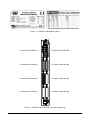
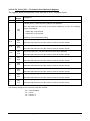
The configuration of the module can be verified by examining the two labels on the cover
of the module. The first label shows the specifications of the motherboard itself, including
the installed options; while the second label shows the configuration of the installed
function cards.
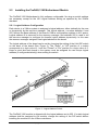
Figure 1 shows an example of a set of module labels for the ProDAQ 3180 motherboard
with a serial number of 512872, which has the optional ProDAQ 3280 TigerSHARC DSP
plug-in with a serial number of 176223 and the ProDAQ 3214 DDR2 SDRAM module with
a serial number of 32140012 installed. Two function cards ProDAQ 3424-AA are installed
in slots 1-3 and 2-4 (the ProDAQ 3424 is a double-wide function card) and a ProDAQ 3550
is installed in slot 5.
3180-XX-UM
Copyright, ©2008 Bustec Production Ltd.
Page 7 of 63
Figure 1 - ProDAQ 3180 Module Labels
Function Card Slot #1
Function Card Slot #2
Function Card Slot #3
Function Card Slot #4
Function Card Slot #5
Function Card Slot #6
Function Card Slot #7
Function Card Slot #8
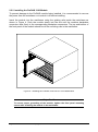
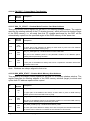
Figure 2 - ProDAQ 3180 Function Card Slot Numbering
Page 8 of 63
Copyright, ©2008 Bustec Production Ltd.
3180-XX-UM
2.2
Installing the ProDAQ 3180 Motherboard Module
The ProDAQ 3150 Motherboard is fully software configurable. No strap or switch settings
are necessary except for the VXI Logical Address setting as specified by the VXIbus
standard.
2.2.1 Logical Address Configuration
Each device in a VXIbus system is assigned a logical address, either statically by the user
or dynamically by the resource manager. This logical address, a number between 0 and
255, defines the base address of the board's VXIbus configuration registers in A16 space.
Logical address 0 is reserved for the resource manager, and address 255 is used to tell
the resource manager to configure the board's logical address dynamically. In this case
the resource manager assigns a free logical address to the board.
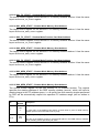
The logical address of the board can be set by changing the setting of the 8-bit DIP switch
on the back of the board (See Figure 3). The "Open" or "Off" position of a switch
corresponds to a logic value of 1 and the "Closed" or "On" position to a logic value of 0.
Keep in mind that each board in the system must be assigned its own unique logical
address (if configured statically) when setting the switch.
8
OFF
1
ON
1
8
LA=3
OFF
ON
1
8
LA=255
OFF
Figure 3 - Logical Address Switch
The ProDAQ 3180 module is shipped with the logical address set to 255. If a static logical
address shall be assigned to the module, change the setting of the DIP switch before
installing the module into the VXIbus mainframe.
3180-XX-UM
Copyright, ©2008 Bustec Production Ltd.
Page 9 of 63
2.2.2 Installing the ProDAQ 3180 Module
To prevent damage to the ProDAQ module being installed, it is recommended to remove
the power from the mainframe or to switch it off before installing.
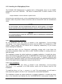
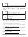
Insert the module into the mainframe using the guiding rails inside the mainframe as
shown in Figure 4. Push the module slowly into the slot until the modules backplane
connectors seat firmly in the corresponding backplane connectors. The top and bottom of
the front panel of the module should touch the mounting rails in the mainframe.
Figure 4 - Installing the ProDAQ 3180 into a C-Size Mainframe
Important:
To ensure proper grounding of the module, tighten the front panel mounting
screws after installing the module in the mainframe.
Page 10 of 63
Copyright, ©2008 Bustec Production Ltd.
3180-XX-UM
2.2.3 Installing the VXIplug&play Driver
The ProDAQ 3180 Motherboard is supplied with a VXIplug&play driver for the WIN32
framework, Linux and VxWorks®. The driver is marked with a version number of the
format
<major release>.<minor release>.<patch level>
As the function card drivers rely on the motherboard driver for the communication with the
function cards, they share common structures and an internal API with the motherboard
driver.
NOTE:
For the function card and motherboard drivers to work together, all installed
drivers must be of the same major and minor version. The patch level may differ.
NOTE:
It is recommended to install the VISA library prior to installing any motherboard
or function card driver.
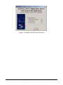
2.2.3.1 WIN32 Framework Installation
On the distribution CD, the driver is located in the subdirectory " \Driver\ProDAQ
3180\WIN32". If you have downloaded the driver from the WEB, it is contained in a ZIP
archive. Please unpack the ZIP archive into a temporary subdirectory of your choice
before starting the installation.
To install the driver, run the “Setup.exe” application coming with it and follow the
instructions presented. Make sure that no other ProDAQ software is running when you
start the setup.
The installation program by default performs a complete installation. It installs the driver
files in the directory tree defined by the %VXIPNPPATH% environment variable and the
shortcuts into the VXIPNP program group of the start menu. To choose a different path
and/or custom installation options is not recommended and may result in malfunctioning of
the soft front panel and any application trying to use the driver.
2.2.3.2 Linux Installation
On the distribution CD, the driver is located in the subdirectory " \Driver\ProDAQ
3180\Linux". It is contained in an RPM archive, which can be directly used for the
installation.
To install the driver, run "rpm –i bu3180-x.x.x.rpm". On most systems, you will need to
have superuser rights or use the "sudo" command for a successful installation.
The installation program by default performs a complete installation. It installs the driver
files in the directory tree defined by the %VXIPNPPATH% environment variable. To
3180-XX-UM
Copyright, ©2008 Bustec Production Ltd.
Page 11 of 63
choose a different path and/or custom installation options is not recommended and may
result in malfunctioning of the soft front panel and any application trying to use the driver.
NOTE:
The installation described here only applies to desktop Linux installations. For
embedded systems using a cross-development environment the installation may
differ. Refer to the cross-development environments documentation for more
information.
2.2.3.3 VxWorks Installation
On the distribution CD, the driver is located in the subdirectory " \Driver\ProDAQ
3180\VxWorks". It is contained in a ZIP archive. In addition to the version number of the
driver, the archive name also shows the version of the VxWorks operating system it is
precompiled for ("vx<major>.<minor>") and the architecture it is compiled for:
bu3180-<major>.<minor>.<patch>-vx<major>.<minor>-<arch>.zip
where <arch> can be for example "<pentium>" or "<ppc>".
The archive contains files with paths relative to the root of the standard VXIplug&play
directory tree. It is recommended to install all drivers into the same subdirectory tree.
Page 12 of 63
Copyright, ©2008 Bustec Production Ltd.
3180-XX-UM
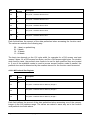
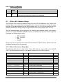
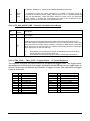
Chapter 3 - Theory of Operation
The ProDAQ 3180 Ultra-performance Motherboard is a single-slot C-size VXIbus module
able to accommodate up to eight ProDAQ function cards, a DSP plug-in, a memory
module and a voltage reference plug-in. It provides the common resources necessary for
these components to be part of a VXIbus system, like for example a VXIbus interface,
common registers and trigger routing.
3.1
Overview
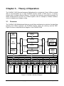
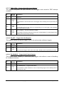
The ProDAQ 3180 Motherboard features a multi-bus architecture to optimize the data flow
between the VXIbus interface, the ProDAQ function cards, the memory and the DSP.
Figure 5 shows a simplified block diagram of the ProDAQ 3180.
DDR2 SDRAM
Memory
(optional)
VXIbus Interface
Power
Supply
Subsystem
Memory
Controller
Data
Transfer
Subsystem
V
B
U
S
DSP
Plug-in Module
(optional)
Common
Registers
Trigger
Distribution
Subsystem
Boot FLASH
16 MByte
P
B
U
S
Voltage
Reference
Plug-in
(optional)
Function Card
Controller
Function Card Bus
Function
Card
Slot
1
Function
Card
Slot
2
Function
Card
Slot
3
Function
Card
Slot
4
Function
Card
Slot
5
Function
Card
Slot
6
Function
Card
Slot
7
Function
Card
Slot
8
Figure 5 - ProDAQ 3180 Block Diagram
3180-XX-UM
Copyright, ©2008 Bustec Production Ltd.
Page 13 of 63
Two high-speed, 32-bit wide internal busses are used to transfer the data between the
different parts of the system. The VBus (VXI-side bus) allows masters on the VXIbus (via
the VXIbus interface) read/write access to the board resources like memory, function cards
and internal registers via the VXIbus interface. It uses a synchronous pipelined protocol
and has a maximum throughput rate of 160 MByte/s. The PBus (Processor-side bus) does
the same for the optional TigerSHARC DSP. To improve the real-time data processing, it
runs at twice the clock frequency of the VBus, allowing for a maximum data throughput of
320 MByte/s.
The memory controller acts as a bus bridge between the VBus/PBus and the standard
DDR2 SDRAM bus. The SDRAM bus can interface single bank memory modules with a
sustained data rate of more then 512 MByte/s. A read/write cache and a special shadow
mode, where data transferred over the PBus to the DSP is shadowed (simultaneously
copied) into a memory bank further improve the overall data throughput.
The up to eight ProDAQ function cards are interfaced to the VBus and PBus via the
function card controller. The function card controller contains two independent bus bridges,
one for accesses from the VBus to the function cards and one for accesses from the PBus
to the function cards to allow simultaneous accesses from both sides to different function
cards. The bus bridges also allow access to more then one function card at the same time
and implement both the standard bus protocol of the existing ProDAQ function cards plus
an enhanced new protocol, pushing the data throughput to a maximum of 320 MByte/s.
3.1.1 The VXIbus Interface
The VXIbus interface consists of three subsystems: the power supply subsystem, which is
responsible to provide clean power to all parts of the system; the data transfer subsystem,
which contains the VXIbus slave and VBus master and forwards all accesses made to the
board by a VXIbus master to the internal VBus; and the trigger distribution subsystem,
which allows to distribute trigger signals between the VXIbus trigger lines, the function
card trigger lines and the DSP plug-in module.
The data transfer subsystem forwards all accesses to the two address ranges used by the
ProDAQ 3180 in the VXIbus A16 and A32 address space onto the internal VBUS. The
VXIbus A16 address range allows access to the configuration registers and can be
accessed using D08(EO)/D16/D32 transactions. The A32 range allows access to the
function cards, the memory and common registers. It supports D16/D32, D16/D32 BLT,
MBLT and 2eVME transactions. To better coordinate the internal data transfer, the data
transfer subsystem utilizes both posted writes and prefetching when accessing the
different internal resources.
NOTE:
In order to use MBLT or 2eVME transactions, the slot-0 controller/VXIbus master
used MUST be able to generate such cycles. Please refer to your slot-0 controller
hardware documentation. In addition the hardware access library/driver used
(e.g. the VISA library) must be able to select such a mode.
The trigger distribution subsystem allows to route trigger signals between the VXIbus TTL
and ECL trigger lines and the function card trigger in/out lines. The trigger events can also
be used to generate a VXIbus interrupt.
Page 14 of 63
Copyright, ©2008 Bustec Production Ltd.
3180-XX-UM
3.1.2 The Memory Controller
The memory controller contains two local bus slaves, one monitoring the transactions on
the VBus, while the other one monitors the transaction on the PBus. The high data
bandwidth of the DDR2 SDRAM together with an internal arbiter allow for nearly
simultaneous accesses to the memory from both busses. A cache controller implements a
write-through cache to further speed up the accesses and translate them into the
necessary burst read/writes for the SDRAM.
Due to the limited size of the ProDAQ 3180s VXIbus A32 address range (256 MByte), the
local bus slave for the VBus maps three windows of 64 MBytes size from the SDRAM
memory space into the VBus space. The start address of each window is programmable.
The local bus slave for the PBus features a special "shadow" mode, where either read
accesses generated by the DSP in the function card address space are simultaneously
copied to the memory or read accesses generated by the DSP for the memory are
simultaneously copied to the function cards. This provides raw data streamed to/from the
function cards to an application program running on the DSP for further processing without
duplicating read/write accesses.
3.1.3 The Function Card Controller
The function card controller implements two complete local bus slaves/function card
interfaces, one for accesses from the VBus and one for accesses from the PBus. An
arbiter coordinates the accesses, allowing simultaneous accesses to different function
cards from the VBus and PBus. Scheduling only occurs if the same function card is
accessed simultaneously from both sides.
Both local bus slaves/function card interfaces implement windows for accesses to single
function cards, windows for simultaneous accesses to two or four function cards and a
special window for broadcast writes to all function cards.
3.2
Modes of Operation
The ProDAQ 3180 Motherboard implements the complete functionality to operate ProDAQ
function cards in a VXIbus system. The application software and function card drivers can
directly access the function card registers to control the cards functions and read/write the
data. However, to reach the maximum performance, the optional DSP plug-in module and
the DDR2 SDRAM memory are utilized to scatter/gather the data to/from the function
cards and allow for an optimized data transfer via the VXIbus.
3.2.1 Direct Function Card Access
When the ProDAQ 3180 Motherboard is used without the ProDAQ 3280 TigerSHARC
DSP Plug-in and the ProDAQ 3214 DDR2 SDRAM option, either because the options are
not installed, the TigerSHARC DSP is used to execute a custom application or just by
choice, the ProDAQ 3180 Motherboard allows direct access to the function cards via its
A32 address range for the function card drivers. The ProDAQ VXIplug&play drivers
automatically detect the availability of the DSP plug-in and memory and switch to direct
access if they are not available.
3180-XX-UM
Copyright, ©2008 Bustec Production Ltd.
Page 15 of 63
3.2.2 DSP-Supported Function Card Access
If the ProDAQ 3280 TigerSHARC DSP Plug-in and the ProDAQ 3214 DDR2 SDRAM
option are installed and available, the ProDAQ function card drivers use the DSP to
execute part of their functionality. These so-called lists can support and speed up common
tasks as for example initialization and set-up as well as data acquisition and generation.
For the later, each function card gets assigned a buffer in the DDR2 SDRAM, which is
used by the driver to de-couple and speed up the data transfer to and from the function
card.
NOTE:
The DSP utilization by the ProDAQ VXIplug&play drivers varies from function
card to function card depending on its functionality. Please refer to the function
card driver documentation for more information.
3.2.3 Custom DSP Applications
ohdoh
Page 16 of 63
Copyright, ©2008 Bustec Production Ltd.
3180-XX-UM
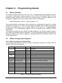
Chapter 4 - Programming Details
4.1
VXIbus Interface
The VXIbus interface conforms to the VXI-1 Rev. 3.0 Specification and supports access to
the boards configuration registers located in the VXIbus A16 address space and the
additional image located in the VXIbus A32 address space. The base address of the
configuration registers in the A16 address space can be calculated by:
A16 Base Address = 49152 + Logical Address * 64
The logical address is determined either statically by configuring the board for a logical
address in the range of 1 to 254 or by the resource manager when configuring the board
for dynamic configuration by using a logical address of 255 (see 2.2.1 : Logical Address
Configuration). The configuration registers can be accessed using D08(EO)/D16/D32
transactions.
The resource manager always assigns the base address of the board's address range in
the VXIbus A32 address space dynamically. The A32 range allows access to the function
cards, the memory and common registers. It supports D16/D32, D16/D32 BLT, MBLT and
2eVME transactions.
4.2
VXIbus Configuration Register
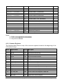
4.2.1 VXIbus Configuration Register Map
The following table shows a map of the VXIbus configuration registers. The offset shown is
relative to the A16 base address.
Offset
0x00
0x02
0x04
0x06
0x08-0x10
0x12
0x14
0x16
0x18
0x1A
0x1C
0x1E
0x20-0x30
0x32
Name
Access
ID
LA
DeviceType
Status
Control
Offset
<reserved>
Interrupt
FC Prefetch Size
MI Prefetch Size
FC Write Threshold
MI Write Threshold
<reserved>
Word Swap
<reserved>
Option Type
0x34-0x3E <reserved>
-
Description
RO
WO
RO
RO
WO
RW
RW
RW
RW
RW
RW
RW
-
ID Register
Logical Address Register
Device Type Register
Status Register
Control Register
Offset Register
Interrupt Control and Status Register
Function Card Prefetch Size Register
Memory Images Prefetch Size Register
Function Card Write Threshold Register
Memory Images Write Threshold Register
Word Swap Control Register
-
RO
Option Type Identification Register
-
Table 1 - VXIbus Configuration Register
3180-XX-UM
Copyright, ©2008 Bustec Production Ltd.
Page 17 of 63
4.2.2 VXIbus Configuration Register Details
4.2.2.1 ID Register
Bit
Access
Default
RO
Description
Device Class
15:14
0x3
This field defines the module as a register based VXIbus device
Address Space
RO
13:12
0x1
This field determines the address ranges used by the device. The ProDAQ 3180
uses a range in the A32 address space in addition to the configuration registers in the
A16 address range.
Manufacturer ID
RO
11:0
0xE70
The Manufacturer ID is 0xE70 and has been assigned by the VXIbus Consortium.
This number uniquely identifies the manufacturer of the device as "Bustec Production
Ltd."
4.2.2.2 Logical Address Register
15:8
Access
Default
-
7:0
WO
Bit
Description
Reserved
Logical Address
Used by the resource manager to assign a logical address to the module during the
dynamic configuration phase. These bits are updated only if DC configuration has
been selected (LA switch set to 255) and MODID line has been asserted for the given
module.
4.2.2.3 Device Type Register
Bit
Access
Default
RO
15:12
Description
Required Memory
0x3
This field defines the window size required by the board in A32 address space. The
value of 0x3 indicates a size of the 256MB.
RO
Model Code
0xC6C
This field contains a unique device identifier: 0xC6C => 3180
11:0
Page 18 of 63
Copyright, ©2008 Bustec Production Ltd.
3180-XX-UM
4.2.2.4 Status Register
Bit
Access
Default
Description
RO
A32 Active
0
This bit reflects the state of the Control register's A32 Enable bit.
15
RO
14
MODID*
H
A one (1) indicates that the device is not selected via the P2 MODID line. A zero (0)
indicates that the device is selected by a high state on the MODID line.
RO
SGLWR_POSTED – Single Write Posted
0
A one (1) indicates the next A32 single write as posted.
-
Reserved
13
12:10
RO
9
H
ROC
8
ITIMEOUT_CLEANUP – Internal Timeout Cleanup
When set this bit indicates that the cleanup after internal timeout is in course and the
board is not accessible in A32 space
ITIMEOUT_HAPPENED – Internal Timeout Happened
H
When set this bit indicates that the internal timeout happened. The bit is cleared after
readout
RO
DSP_AVAIL – DSP Board available
H
When set this bit indicates that the ProDAQ 3280 DSP board is installed.
-
Reserved
RO
DSP_RES – DSP Reset
H
This bit reflects the state of the DSP_RES bit
RO
DSP_RDY – DSP Ready
H
A one (1) indicates that the DSP finished the booting.
7
6
5
4
RO
3
H
Ready
A zero (0) indicates that the module has not completed its initialization process and is
executing its self-test.
Passed
RO
2
1
H
After the self-test completion (signaled by a one (1) in the Ready bit), the Passed bit
indicates the status of the self-test. A one (1) indicates that the self-test has
successfully completed. A zero (0) means that the device has failed its self-test.
-
Reserved
RO
0
0
3180-XX-UM
SOFT_RESET – Software Reset
This bit reflects the state of the SOFT_RESET: if set then the software reset is in
course
Copyright, ©2008 Bustec Production Ltd.
Page 19 of 63
4.2.2.5 Control Register
Bit
Access
Default
WO
15
14
Description
A32 Active
0
Writing a one (1) to the bit enables accesses to the A32 address space. Writing a
zero (0) disables accesses to the A32 address space.
-
Reserved
SGLWR_POSTED – Single Write Posted
WO
13
12:6
1
A zero (0) written to this bit defines the single writes as non-posted. It means that VXI
bus slave waits with the A32 single write completion until it gets confirmation from FC
or Common Registers controller that the word reached the destination.
-
Reserved
DSP_RES – DSP Reset
WO
5
4:2
1
A one (1) written to this bit place the DSP in reset. After power up the host has to
release the reset to let the DSP start booting. Releasing reset after power on could
be done automatically if DSP_STANDALONE_N bit in the EEPROM is set to zero.
-
Reserved
WO
Sysfail Inhibit
0
A one (1) written to this bit disables the device from driving the SYSFAIL* line.
1
SOFT_RESET – Software Reset
WO
0
0
Writing a one (1) to the bit reset the module (device goes into reset state). Writing a
zero (0) clears the reset.
SOFT_RESET clears all state machines and all registers in Common Register
address space but A16 Slave and some Configuration Registers are not affected by
this reset
4.2.2.6 Offset Register
Bit
Access
Default
RW
15:12
0
Page 20 of 63
Description
Offset
The bits define the base address of the device in the VXI A32 address space. The
bits 15:12 are mapped to the address lines A31:A28
Copyright, ©2008 Bustec Production Ltd.
3180-XX-UM
4.2.2.7 Interrupt Register
Bit
Access
Default
RO
15:9
H
Description
IRQ_STS[7:1] – IRQ Status
Shows the status of the VXI IRQ lines. A value of ‘1’ means the interrupt line is
asserted.
IRQ_CLR[2:0] – IRQ Clear
8:6
WO
Writing ‘101’ to these bits clears the IRQ output of the interrupter.
SW_INT – Software Interrupt
RWC
5
0
RW
4
0
RW
3
0
The bit is used to generate the interrupt to the VXI bus. When the bit is set the
interrupt is generated to the selected IRQ line, The bit is cleared by hardware at the
end of the IACK cycle.
MBOX_INT_EN – Mailbox Interrupt Enable
The bit is used to enable/disable the mailbox as a source of the interrupt to the VXI
bus. When the bit is set this source of the interrupt is enabled.
TNODE_INT_EN – Trigger Node Interrupt Enable
The bit is used to enable/disable Trigger Node 20 as a source of the interrupt to the
VXI bus. When the bit is set this source of the interrupt is enabled.
IRQ_LEVEL[2:0] – IRQ Level
The bits select the VXI IRQ line of the interrupter.
The values are coded in the following way:
RW
2:0
0
000 : Interrupts disabled
001 : IRQ1 selected
010 : IRQ2 selected
011 : IRQ3 selected
100 : IRQ4 selected
101 : IRQ5 selected
110 : IRQ6 selected
111 : IRQ7 selected
4.2.2.8 FC Prefetch Size Register
Bit
Access
Default
RW
Description
PFS_FC8 – Prefetch Size for FC8
15:14
0
RW
PFS_FC7 – Prefetch Size for FC7
13:12
0
RW
PFS_FC6 – Prefetch Size fo FC6
11:10
0
3180-XX-UM
Copyright, ©2008 Bustec Production Ltd.
Page 21 of 63
Bit
Access
Default
RW
Description
PFS_FC5 – Prefetch Size for FC5
9:8
0
RW
PFS_FC4 – Prefetch Size for FC4
7:6
0
RW
PFS_FC3 – Prefetch Size of FC3
5:4
0
RW
PFS_FC2 – Prefetch Size of FC2
3:2
0
1:0
RW
0
PFS_FC1 – Prefetch Size of FC1
Each field defines the amount of the data prefetched when accessing the function card.
The values are coded in the following way:
00 : 1 beat, no prefetching
01 : 8 beats
10 : 16 beats
11 : 64 beats
The beat size depends on the VXI cycle width, for example for a D16 access one beat
means 2 bytes, for a D32 access four bytes, and for a D64 access eight bytes. For doublewide function cards, the prefetch size needs to be set for both positions they are located
in. If one of the available modes is used to access several function cards in parallel, the
prefetch size used is determined by the smallest size set for the function cards accessed.
4.2.2.9 MI Prefetch Size Register
Bit
Access
Default
Description
15:6
-
Reserved
RW
PFS_MI3 – Prefetch Size for Memory Image 3
5:4
0
RW
PFS_MI2 – Prefetch Size for Memory Image 2
3:2
0
RW
PFS_MI2 – Prefetch Size for Memory Image 1
1:0
0
Each field defines the amount of the data prefetched when accessing one of the memory
images in the A32 address range. The values are coded in same way as in the function
card prefetch size fields above.
Page 22 of 63
Copyright, ©2008 Bustec Production Ltd.
3180-XX-UM
4.2.2.10 FC Write Threshold Register
Bit
Access &
Description
Default
RW
WTH_FC8 – Write Threshold for FC8
15:14
0
RW
WTH_FC7 – Write Threshold for FC7
13:12
0
RW
WTH_FC6 – Write Threshold for FC6
11:10
0
RW
WTH_FC5 – Write Threshold for FC5
9:8
0
RW
WTH_FC4 – Write Threshold for FC4
7:6
0
RW
WTH_FC4 – Write Threshold for FC3
5:4
0
RW
WTH_FC4 – Write Threshold for FC2
3:2
0
RW
WTH_FC4 – Write Threshold for FC1
1:0
0
Each field defines the amount of the data buffered before accessing a function card. The
values are coded in the following way:
00 : 1 beat
01 : 8 beats
10 : 16 beats
11 : 64 beats
The beat size depends on the VXI cycle width, for example for a D16 access one beat
means 2 bytes, for a D32 access four bytes, and for a D64 access eight bytes. For doublewide function cards, the write threshold size needs to be set for both positions they are
located in. If one of the available modes is used to access several function cards in
parallel, the write threshold size used is determined by the smallest size set for the
function cards accessed.
3180-XX-UM
Copyright, ©2008 Bustec Production Ltd.
Page 23 of 63
4.2.2.11 MI Write Threshold register
Bit
Access &
Description
Default
15:6
-
Reserved
RW
WTH_MI3 – Write Threshold of Memory Image 3
5:4
0
RW
WTH_MI3 – Write Threshold of Memory Image 2
3:2
0
RW
WTH_MI3 – Write Threshold of Memory Image 1
1:0
0
Each field defines the amount of the data buffered before accessing one of the memory
images in the A32 address range. The values are coded in same way as in the function
card write threshold size fields above.
4.2.2.12 Word Swap Register
This register is used to configure the word swapping used for D32, MBLT and 2eVME
accesses. The word swapping logic swaps the upper 16-bit word with the lower 16-bit
word for D32 access. For MBLT and 2eVME accesses it swaps the two upper words with
each other and the two lower words in the same way. Word swapping works for read and
write accesses.
Bit
Access
Default
Description
15
-
Reserved
WSWAP_QW4 – Word Swap, QW window of FC5-6-7-8
RW
14
0
When this bit is set the 16-bit word swapping happens during D64 accesses to the
QW window of the FC5-6-7-8. For the D64 first 16-bit word is swapped with the
second word, and third word is swapped with the fourth word of the 64-bit data.
WSWAP_QW3 – Word Swap, QW window of FC1-2-3-4
RW
13
0
When this bit is set the 16-bit word swapping happens during D64 accesses to the
QW window of the FC1-2-3-4. For the D64 first 16-bit word is swapped with the
second word, and third word is swapped with the fourth word of the 64-bit data.
WSWAP_QW2 – Word Swap, QW window of FC2-4-6-8
RW
12
0
When this bit is set the 16-bit word swapping happens during D64 accesses to the
QW window of the FC2-4-6-8. For the D64 first 16-bit word is swapped with the
second word, and third word is swapped with the fourth word of the 64-bit data.
WSWAP_QW1 – Word Swap, QW window of FC1-3-5-7
RW
11
0
Page 24 of 63
When this bit is set the 16-bit word swapping happens during D64 accesses to the
QW window of the FC1-3-5-7. For the D64 first 16-bit word is swapped with the
second word, and third word is swapped with the fourth word of the 64-bit data.
Copyright, ©2008 Bustec Production Ltd.
3180-XX-UM
Bit
Access
Default
Description
WSWAP_DW8 – Word Swap, DW window of FC7-8
RW
10
0
When this bit is set the 16-bit word swapping happens during D32 or D64 accesses
to the DW window of the FC7-8. For the D64 first 16-bit word is swapped with the
second word, and third word is swapped with the fourth word of the 64-bit data.
WSWAP_DW7 – Word Swap, DW window of FC5-6
RW
9
0
When this bit is set the 16-bit word swapping happens during D32 or D64 accesses
to the DW window of the FC5-6. For the D64 first 16-bit word is swapped with the
second word, and third word is swapped with the fourth word of the 64-bit data.
WSWAP_DW6 – Word Swap, DW window of FC3-4
RW
8
0
When this bit is set the 16-bit word swapping happens during D32 or D64 accesses
to the DW window of the FC3-4. For the D64 first 16-bit word is swapped with the
second word, and third word is swapped with the fourth word of the 64-bit data.
WSWAP_DW5 – Word Swap, DW window of FC1-2
RW
7
0
When this bit is set the 16-bit word swapping happens during D32 or D64 accesses
to the DW window of the FC1-2. For the D64 first 16-bit word is swapped with the
second word, and third word is swapped with the fourth word of the 64-bit data.
WSWAP_DW4 – Word Swap, DW window of FC6-8
RW
6
0
When this bit is set the 16-bit word swapping happens during D32 or D64 accesses
to the DW window of the FC6-8. For the D64 first 16-bit word is swapped with the
second word, and third word is swapped with the fourth word of the 64-bit data.
WSWAP_DW3 – Word Swap, DW window of FC5-7
RW
5
0
When this bit is set the 16-bit word swapping happens during D32 or D64 accesses
to the DW window of the FC5-7. For the D64 first 16-bit word is swapped with the
second word, and third word is swapped with the fourth word of the 64-bit data.
WSWAP_DW2 – Word Swap, DW window of FC2-4
RW
4
0
When this bit is set the 16-bit word swapping happens during D32 or D64 accesses
to the DW window of the FC2-4. For the D64 first 16-bit word is swapped with the
second word, and third word is swapped with the fourth word of the 64-bit data.
WSWAP_DW1 – Word Swap, DW window of FC1-3
RW
3
0
When this bit is set the 16-bit word swapping happens during D32 or D64 accesses
to the DW window of the FC1-3. For the D64 first 16-bit word is swapped with the
second word, and third word is swapped with the fourth word of the 64-bit data.
WSWAP_MI3 – Word Swap, Memory Image 3
RW
2
0
When this bit is set the 16-bit word swapping happens during D32 or D64 accesses
to Memory Image 3. For the D64 first 16-bit word is swapped with the second word,
and third word is swapped with the fourth word of the 64-bit data.
WSWAP_MI2 – Word Swap, Memory Image 2
RW
1
0
3180-XX-UM
When this bit is set the 16-bit word swapping happens during D32 or D64 accesses
to Memory Image 2. For the D64 first 16-bit word is swapped with the second word,
and third word is swapped with the fourth word of the 64-bit data.
Copyright, ©2008 Bustec Production Ltd.
Page 25 of 63
4.2.2.13 Option Type Register
Bit
15:8
7:0
4.3
Access &
Default
RO
0
Description
Reserved
OPTION_TYPE
The bits show the option type installed in the motherboard.
VXIbus A32 Address Range
The ProDAQ 3180 utilizes an address range of the size of 256 MBytes in the VXIbus A32
address space. Its base address is assigned by the resource manager by writing the upper
four bits of the base address into the offset register (see 4.2.2.6) and by enabling the A32
address decoding by writing to the "A32 Active" bit in the control register (see 4.2.2.5).
The A32 address range offers access to the function card address ranges, the memory
windows to access the DDR2 SDRAM memory (if installed) and a set of control registers.
It accepts the following bus cycles:
-
SCT: D16/D32
BLT: D16/D32
MBLT
2eVME
Some areas do not support D16 and/or D32 accesses as shown below. Please note that
unaligned transfers are not supported.
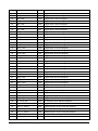
4.3.1 VXIbus A32 Address Range Map
The following table shows a map of the VXIbus A32 address range used by the ProDAQ
3180. The offset shown is relative to the base address set in the offset register.
Offset Range
Size [kB] Description
0x0000000 - 0x1FFFFFF
128
Common Registers
0x2000000 - 0x201FFFF
128
Function Card 1, SW window
0x2020000 - 0x203FFFF
128
Function Card 2, SW window
0x2040000 - 0x205FFFF
128
Function Card 3, SW window
0x2060000 - 0x207FFFF
128
Function Card 4, SW window
0x2080000 - 0x209FFFF
128
Function Card 5, SW window
0x20A0000 - 0x20BFFFF
128
Function Card 6, SW window
0x20C0000 - 0x20DFFFF
128
Function Card 7, SW window
0x20E0000 - 0x20FFFFF
128
Function Card 8, SW window
0x2100000 - 0x21FFFFF
-
reserved
0x2200000 - 0x223FFFF
256
Function Cards 1-3, DW window
1
0x2240000 - 0x227FFFF
256
Function Cards 2-4, DW window
1
Page 26 of 63
Copyright, ©2008 Bustec Production Ltd.
Notes
3180-XX-UM
Offset Range
Size [kB] Description
Notes
0x2280000 - 0x22BFFFF
256
Function Cards 5-7, DW window
1
0x22C0000 - 0x22FFFFF
256
Function Cards 6-8, DW window
1
0x2300000 - 0x233FFFF
256
Function Cards 1-2, DW window
1
0x2340000 - 0x237FFFF
256
Function Cards 3-4, DW window
1
0x2380000 - 0x23BFFFF
256
Function Cards 5-6, DW window
1
0x23C0000 - 0x23FFFFF
256
Function Cards 7-8, DW window
1
0x2400000 - 0x247FFFF
512
Function Cards 1-3-5-7, QW window
1,2
0x2480000 - 0x24FFFFF
512
Function Cards 2-4-6-8, QW window
1,2
0x2500000 - 0x257FFFF
512
Function Cards 1-2-3-4, QW window
1,2
0x2580000 - 0x25FFFFF
512
Function Cards 5-6-7-8, QW window
1,2
0x2600000 - 0x261FFFF
128
Function Cards, BW window
3
0x2620000 - 0x3FFFFFF
-
reserved
0x4000000 - 0x7FFFFFF
65536
DDR Memory Window 1
0x8000000 - 0xBFFFFFF
65536
DDR Memory Window 2
0xC000000 - 0xFFFFFFF
65536
DDR Memory Window 3
Notes:
1 - D16 is not supported for this window
2 - D32 is not supported for this window
3 - Only write is allowed
4.3.2 Common Registers
The following table shows a map of the common registers located at the beginning of the
A32 address range.
Offset
Register Name
Access Description
0
MB_REV
RO
Motherboard Revision
4
MB_SN
RO
Motherboard Serial Number
8
PB_REV
RW
Plug-in Board Revision
C
PB_SN
RO
Plug-in Board Serial Number
10
VREF_REV
RO
Voltage Reference Revision
14
VREF_SN
RO
Voltage Reference Serial Number
18
I2C_BUS1_CTRL
RW
I2C bus #1 control register
1C
I2C_BUS2_CTRL
RW
I2C bus #2 control register
20
JTAG_CTRL
RW
JTAG chain control register
24
FC_HSDET
RO
Function Card High-Speed Detection register
28
FC_RST
RW
Function Card Reset register
2C
FC_CTRL_VXI
RW
Function Card Control Register for VXI side
30
FC_CTRL_DSP
RW
Function Card Control Register for DSP side
34
FC_WR_QUEUE_EMP
RO
Function Card Write Queue Empty
38
TN0_CTRL
RW
Trigger Node 0 Control Register
3180-XX-UM
Copyright, ©2008 Bustec Production Ltd.
Page 27 of 63
Offset
Register Name
Access Description
3C
TN1_CTRL
RW
Trigger Node 1 Control Register
40
TN2_CTRL
RW
Trigger Node 2 Control Register
44
TN3_CTRL
RW
Trigger Node 3 Control Register
48
TN4_CTRL
RW
Trigger Node 4 Control Register
4C
TN5_CTRL
RW
Trigger Node 5 Control Register
50
TN6_CTRL
RW
Trigger Node 6 Control Register
54
TN7_CTRL
RW
Trigger Node 7 Control Register
58
TN8_CTRL
RW
Trigger Node 8 Control Register
5C
TN9_CTRL
RW
Trigger Node 9 Control Register
60
TN10_CTRL
RW
Trigger Node 10 Control Register
64
TN11_CTRL
RW
Trigger Node 11 Control Register
68
TN12_CTRL
RW
Trigger Node 12 Control Register
6C
TN13_CTRL
RW
Trigger Node 13 Control Register
70
TN14_CTRL
RW
Trigger Node 14 Control Register
74
TN15_CTRL
RW
Trigger Node 15 Control Register
78
TN16_CTRL
RW
Trigger Node 16 Control Register
7C
TN17_CTRL
RW
Trigger Node 17 Control Register
80
TN18_CTRL
RW
Trigger Node 18 Control Register
84
TN19_CTRL
RW
Trigger Node 19 Control Register
88
TN20_CTRL
RW
Trigger Node 20 Control Register
8C
TN21_CTRL
RW
Trigger Node 21 Control Register
90
TN22_CTRL
RW
Trigger Node 22 Control Register
94
TN23_CTRL
RW
Trigger Node 23 Control Register
98
TN24_CTRL
RW
Trigger Node 24 Control Register
9C
TN25_CTRL
RW
Trigger Node 25 Control Register
A0
TN26_CTRL
RW
Trigger Node 26 Control Register
A4
TN27_CTRL
RW
Trigger Node 27 Control Register
A8
TN28_CTRL
RW
Trigger Node 28 Control Register
AC
TN_SET
RW
Trigger Node Set Register
B0
TN_ENABLE
RW
Trigger Node Enable Register
B4
TN_STATUS
RO
Trigger Node Status
B8
TN_SRC_STATUS1
RO
Trigger Node Source Status Register 1
BC
TN_SRC_STATUS2
RO
Trigger Node Source Status Register 2
C0
FC_CCLK_SEL
RW
FC Common Clock Selection Register
C4
TM_TEST
RW
Trigger Matrix Test Register
C8
SH0_FC_START
RW
Shadow Mode Function Card Start Address
CC
SH0_MEM_START
RW
Shadow Mode Memory Start Address
D0
SH1_FC_START
RW
Shadow Mode Function Card Start Address
D4
SH1_MEM_START
RW
Shadow Mode Memory Start Address
D8
SH2_FC_START
RW
Shadow Mode Function Card Start Address
Page 28 of 63
Copyright, ©2008 Bustec Production Ltd.
3180-XX-UM
Offset
Register Name
Access Description
DC
SH2_MEM_START
RW
Shadow Mode Memory Start Address
E0
SH3_FC_START
RW
Shadow Mode Function Card Start Address
E4
SH3_MEM_START
RW
Shadow Mode Memory Start Address
E8
SH4_MEM_START
RW
Shadow Mode Memory Start Address
EC
SH4_FC_START
RW
Shadow Mode Function Card Start Address
F0
SH5_MEM_START
RW
Shadow Mode Memory Start Address
F4
SH5_FC_START
RW
Shadow Mode Function Card Start Address
F8
SH6_MEM_START
RW
Shadow Mode Memory Start Address
FC
SH6_FC_START
RW
Shadow Mode Function Card Start Address
100
SH7_MEM_START
RW
Shadow Mode Memory Start Address
104
SH7_FC_START
RW
Shadow Mode Function Card Start Address
108
SH_CTRL
RW
Shadow Mode Control Register
10C
DDR_PAGE_IMAGE1
RW
DDR Memory Page Image 1 Offset Register
110
DDR_PAGE_IMAGE2
RW
DDR Memory Page Image 2 Offset Register
114
DDR_PAGE_IMAGE3
RW
DDR Memory Page Image 3 Offset Register
118
DDR_CTRL
RW
DDR Memory Control Register
11C
LBUS_CTRL
RW
Local Bus control register
120
ERROR
RW
ERROR status register
124
TEST
RW
R/W Test Register
128
Reserved
RW
Mailbox VXI to DSP Register
…
…
1FC
Reserved
200
MBOX_VXI2DSP0
…
…
…
…
2F8
MBOX_VXI2DSP62
RW
Mailbox VXI to DSP Register
2FC
MBOX_VXI2DSP63
RW
Mailbox VXI to DSP Register
300
MBOX_DSP2VXI0
RW
Mailbox DSP to VXI Register
…
…
…
…
3F8
MBOX_DSP2VXI62
RW
Mailbox DSP to VXI Register
3FC
MBOX_DSP2VXI63
RW
Mailbox DSP to VXI Register
400
LBUS_FIFO
RW
Local Bus FIFO port
NOTE:
Changing values in the common registers directly may result in rendering the
board unusable. It is strongly recommended to use the VXIplug&play driver
functions instead.
3180-XX-UM
Copyright, ©2008 Bustec Production Ltd.
Page 29 of 63
4.3.3 Common Register Details
4.3.3.1 MB_REV – Motherboard Revision
This register provides information about hardware revision of the motherboard.
Bit
31:24
Access
Default
RO
H
23:16
RO
H
7:0
RO
H
Description
MB_SUBTYPE
Subtype number loaded from the on-board EEPROM memory
MB_PCB_REV – MB PCB Revision Number
Motherboard’s PCB design revision number, lower 4 bits define minor revision
change and upper 4 bits define major revision change.
FPGA1_REV[7:0] – FPGA 1 Revision Number
The revision of the FPGA1 (main FPGA). Lower 4 bits define minor revision change
and upper 4 bits define major revision change.
4.3.3.2 MB_SN – Motherboard Serial Number
This register contains motherboard’s serial number. This register is automatically loaded
during board initialization with contents of the on-board EEPROM chip.
Bit
31:0
Access
Default
RO
H
Description
MB_SN
Serial number loaded from the on-board EEPROM memory
4.3.3.3 PB_REV – Plug-in Board Revision
This register provides information about hardware/firmware revision of the Plug-in Board.
Bit
Access
Default
Description
RO
H
PB_SUBTYPE
Subtype number is loaded from the EEPROM memory fitted on the Plug-in Board.
It is valid only when Plug-in Board is fitted (PB_FITTED bit in configuration register’s
Status Register is ‘1’)
23:16
RO
H
PB_PCB_REV – PB PCB Revision Number
Plug-in Board PCB design revision number, lower 4 bits define minor revision change
and upper 4 bits define major revision change.
It is valid only when Plug-in Board is fitted (PB_FITTED bit in configuration register’s
Status Register is ‘1’)
15:8
PRW
VRO
H
SILICON_REV[7:0] – DSP silicon revision
The revision of the DSP silicon. Lower four bits define minor revision change and
upper four bits define major revision change.
7:0
PRW
VRO
H
FIRM_REV[7:0] – DSP firmware revision
The revision of the DSP firmware. Lower four bits define minor revision change and
upper four bits define major revision change.
31:24
Page 30 of 63
Copyright, ©2008 Bustec Production Ltd.
3180-XX-UM
4.3.3.4 PB_SN – Plug-in Board serial number
This register contains Plug-in Board serial number. This register is automatically loaded
during board initialization with contents of the EEPROM fitted on the Plug-in Board. The
contents of this register is valid only when the Plug-in Board is fitted (PB_FITTED bit in
configuration register’s Status Register is ‘1’)
Bit
31:0
Access
Default
RO
H
Description
PB_SN – Plug-in Board Serial Number
4.3.3.5 VREF_REV – Voltage Reference Revision
This register provides information about type and hardware revision of the Voltage
Reference plug-in board.
Bit
Access
Default
31:25
Description
NOT USED
24
RO
H
VREF_DET – VREF Detected
This bit informs if the VREF board is plugged in.
'0' – VREF board not present
'1' – VREF board plugged in
23:16
RO
H
VREF_TYPE – Voltage Reference Board Type
Type of Voltage Reference Plug-in board (e.g. 3202). Type number is loaded from
the EEPROM memory fitted on the Voltage Reference board (It is valid only when
VREF_DET=’1’)
15:8
7:0
RO
H
RO
H
VREF_SUBTYPE – Voltage Reference Board Type
Subtype number is loaded from the EEPROM memory fitted on the Voltage
Reference board (It is valid only when VREF_DET=’1’)
VREF_PCB_REV – Voltage Reference PCB revision
Voltage Reference Board PCB design revision number, lower 4 bits define minor
revision change and upper 4 bits define major revision change (it is valid only when
VREF_DET=’1’). Currently no VREF board gives information about its PCB revision,
so that this field should not be used.
4.3.3.6 VREF_SN – Voltage Reference board serial number
This register contains Voltage Reference Board serial number. This register is automatically loaded during board initialization with contents of the EEPROM fitted on the
Voltage Reference board. The contents of this register are valid only when the VREF_DET
bit in VREF_REV register is ‘1’.
Bit
31:0
3180-XX-UM
Access
Default
RO
H
Description
VREF_SN – Voltage Reference Board Serial Number
Copyright, ©2008 Bustec Production Ltd.
Page 31 of 63
4.3.3.7 I2C_BUS1_CTRL – I2C Bus #1 Control
Bit
Access
Default
RO
H
31:0
Description
<Internal use only>
4.3.3.8 I2C_BUS2_CTRL – I2C Bus #2 Control
Bit
Access
Default
RO
H
31:0
Description
<Internal use only>
4.3.3.9 JTAG_CTRL – JTAG Chain Control Register
Bit
Access
Default
RO
H
31:0
Description
<Internal use only>
4.3.3.10 FC_HSDET – Function Card High-Speed Detection register
This register shows information about the function cards fitted onto the motherboard.
Bit
Access
Default
31:16
Description
NOT USED
15:14
RO
H
FC8_HSDET[1:0] – High-Speed Detection of the FC8
The bits show the speed detected for function card #8.
13:12
RO
H
FC8_HSDET[1:0] – High-Speed Detection of the FC7
The bits show the speed detected for function card #7.
11:10
RO
H
FC8_HSDET[1:0] – High-Speed Detection of the FC6
The bits show the speed detected for function card #6.
9:8
RO
H
FC8_HSDET[1:0] – High-Speed Detection of the FC5
The bits show the speed detected for function card #5.
7:6
RO
H
FC8_HSDET[1:0] – High-Speed Detection of the FC4
The bits show the speed detected for function card #4.
5:4
RO
H
FC8_HSDET[1:0] – High-Speed Detection of the FC3
The bits show the speed detected for function card #3.
3:2
RO
H
FC8_HSDET[1:0] – High-Speed Detection of the FC2
The bits show the speed detected for function card #2.
1:0
RO
H
FC8_HSDET[1:0] – High-Speed Detection of the FC1
The bits show the speed detected for function card #1.
Page 32 of 63
Copyright, ©2008 Bustec Production Ltd.
3180-XX-UM
The speed status is encoded as:
‘00’ : single width, high-speed FC
‘01’ : double width, high-speed FC
‘10’ : standard-speed FC or not fitted
‘11’ : reserved
4.3.3.11 FC_RST – Function Card Reset register
This register allows resetting function cards and also gives information about fitted function
cards.
Bit
Access
Default
31:16
Description
NOT USED
FC_AVAIL[8:1] – Function Card Available
15:8
RO
H
These bits show the readiness of the function cards to work. When set the FC is
present and ready to work. FC_AVAIL[1] corresponds to the FC1 while FC_AVAIL[8]
corresponds to the FC8.
FC_RESET[8:1] – Function Card Reset
The bits control the reset of the function cards. The reset line of the FC gets asserted
immediately after the corresponding FC_RESET bit was set (FC_RESET[1]
corresponds to the reset line of the FC1 while FC_RESET[8] corresponds to the reset
line of the FC8). To release function card reset, the FC_RESET should be written
with ‘0’ and then polled until it reads ‘0’ (if there were outstanding posted writes in the
write queues to the function card being reset, it takes some time to flush them. This is
required to avoid unwanted data to be written to function card after the reset was
removed).
Write
7:0
RW
0xFF
'0' : Release Function card reset
'1' : Reset the function card
Read
'0' : Function Card reset released
'1' : Function card reset in progress
USAGE
If reset of one of the function cards is released, releasing reset of the next function
card while the corresponding FC_RESET bit of the first function card has not yet
been cleared causes that the first function card is kept is reset until FC_RESET bit of
the second function card has been cleared (both FC_RESET bits are cleared at the
same time). This is because function card controller ensures that all posted writes
present in the queue at the moment when the last FC_RESET has been released are
flushed and is not able to monitor this queue separately for each function card.
3180-XX-UM
Copyright, ©2008 Bustec Production Ltd.
Page 33 of 63
4.3.3.12 FC_CTRL_VXI – Function Card Control Register for VXI side
FC_CTRL_VXI register configures the FC controller for accessing function cards from the
VXI side.
Bit
Access
Default
31:19
Description
NOT USED
FC_ARB_TIMEOUT – Function Card Arbiter Timeout for VXI side
19:18
PRO
VRW
‘00’
It sets a guaranteed time for which the VXI side may hold the FC while other side
(DSP) also needs it. Defines the timeout after which the arbiter grants a function card
to DSP side while both sides have pending transactions to the same FC. The time
starts counting from granting the particular FC to the VXI side.
‘00’ – 250ns
‘01’ – 500ns
‘10’ – 1us
‘11’ – 2us
Reading returns set value.
FC_DATA_TIMEOUT – Function Card Data Timeout for VXI side
Defines the time without a FC access requests pending in the FC controller of the VXI
side after which the arbiter can pass over control to the DSP side as soon as request
to one or more of the function cards currently owned by VXI side appeared (without
waiting for FC_ARB_TIMEOUT).
17:16
PRO
VRW
‘00’
‘00’ – 0ns (instantly after FC controller executed all pending access requests)
‘01’ – 50ns
‘10’ – 100ns
‘11’ – 200ns
Reading returns set value.
USAGE
This timeout is implemented in order not to give control to the other side when only a
short break in the block happened.
FC_WORD_SWAP[8:1] – Function Card Word Swapping for VXI side
When set enables the word swapping for corresponding FC if 32-bit VXI transfers
happen to ‘SW’ (single width window Function Cards) address range.
15:8
PRO
VRW
0x00
‘0’ :
data from the first FC access is put on D15..D0 of 32 bit bus,
data from the second FC access is put on D31..D16 of 32 bit bus
‘1’ :
data from the first FC access is put on D31..D16 of 32 bit bus,
data from the second FC access is put on D15..D0 of 32 bit bus
Reading returns set value.
Page 34 of 63
Copyright, ©2008 Bustec Production Ltd.
3180-XX-UM
4.3.3.13 FC_CTRL_DSP – Function Card Control Register for DSP side
FC_CTRL_DSP register configures the FC controller for accessing function cards from the
DSP side.
Bit
Access
Default
31:24
PRW
VRO
0x00
23:19
-
Description
FC_PACK[8:1] – Function Card Pack
If set enables packed DSP transfers for corresponding FC, i.e. one 32-bit DSP cycle
generates two 16-bit FC cycles. The setting affects only ‘SW’ window. Reading
returns set value.
<not used>
FC_ARB_TIMEOUT – Function Card Arbiter For DSP Timeout
19:18
PRW
VRO
‘00’
It sets a guaranteed time for which the DSP side may hold the FC while other side
(VXI) also needs it. Defines the timeout after which the arbiter grants a Function Card
to VXI side while both sides have outstanding transactions to the same FC. The time
starts counting from granting the particular FC for DSP side.
‘00’ – 250ns
‘01’ – 500ns
‘10’ – 1us
‘11’ – 2us
Reading returns set value.
FC_DSP_DATA_TIMEOUT – Function Card DSP Data Timeout
Defines the time without a FC access requests pending in the FC controller of the
DSP side after which the arbiter can pas over control over FCs to the VXI side as
soon as request to one or more of the function cards currently owned by DSP side
appeared (without waiting for FC_ARB_TIMEOUT).
17:16
PRW
VRO
‘00’
‘00’ – 0ns (instantly after FC controller executed all pending access requests)
‘01’ – 50ns
‘10’ – 100ns
‘11’ – 200ns
Reading returns set value.
USAGE
This timeout is implemented in order not to give control to the other side when only a
short break in the block happened.
FC_WORD_SWAP[8:1] – Function Card Word Swapping for DSP side
When set enables the word swapping for corresponding FC if packed DSP transfers
are selected. The setting affects only ‘SW’ window.
15:8
PRW
VRO
0x00
‘0’ :
‘1’ :
data from the first FC access is put on D15..D0 of 32 bit bus,
data from the second FC access is put on D31..D16 of 32 bit bus
data from the first FC access is put on D31..D16 of 32 bit bus,
data from the second FC access is put on D15..D0 of 32 bit bus
Reading returns set value.
3180-XX-UM
Copyright, ©2008 Bustec Production Ltd.
Page 35 of 63
FC_BCAST_MASK[8:1] – Function Card Broadcast Mask for DSP side
PRW
VRO
0x00
7:0
It is possible to issue the same command to a number of Function Cards by
accessing the broadcast window (‘BW’) address space of FCs. It guarantees that all
writes are simultaneous. These bits select which FCs take part in the broadcast
access. Setting ‘1’ enables the corresponding FC card for the broadcast access.
Reading returns the current state of the broadcast mask.
4.3.3.14 FC_WR_QUEUE_EMP – Function Card Write Queue Empty
Access
Default
Bit
31:1
Description
NOT USED
FC_WR_QUEUE_EMP – Function Card Write Queue Empty
Reading this bit returns information about state of the internal write queue to FCs
(there still might be outstanding write accesses in one of onboard FIFOs if they have
been performed as posted writes). Readout executed by DSP returns information
about write queue on the DSP side only, readout executed by VXI returns information
about write queue on the VXI side only.
RO
‘1’
0
‘0’ –
‘1’ –
Write Queue is not empty (there are still outstanding accesses in the write
queue that didn’t reach function cards yet)
Write Queue is empty (all previous FC writes reached their destination)
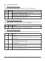
4.3.3.15 TN0_CTRL … TN15_CTRL – Trigger Node 0 ... 15 Control Registers
The registers configure the input sources for the particular trigger node. The trigger nodes
are assigned in the way that each trigger destination on the MB has its own trigger node (a
source), which may be asserted by a number of trigger sources. The destination of trigger
nodes is as follows:
TN0
TN1
TN2
TN3
TN4
TN5
TN6
TN7
TN8
TN9
TN10
TN15
Page 36 of 63
-
FC_TRIGI_A1
FC_TRIGI_A2
FC_TRIGI_A3
FC_TRIGI_A4
FC_TRIGI_A5
FC_TRIGI_A6
FC_TRIGI_A7
FC_TRIGI_A8
FC_TRIGI_B1
FC_TRIGI_B2
FC_TRIGI_B3
FC_TRIGI_B8
TN16
TN17
TN18
TN19
TN20
TN21
TN22
TN23
TN24
TN25
TN26
-
Copyright, ©2008 Bustec Production Ltd.
VXI_TTL_TRG0
VXI_TTL_TRG1
VXI_TTL_TRG2
VXI_TTL_TRG3
VXI_TTL_TRG4
VXI_TTL_TRG5
VXI_TTL_TRG6
VXI_TTL_TRG7
VXI_ECL_TRG0
VXI_ECL_TRG1
FCTRG_2_IRQ
3180-XX-UM
All trigger nodes from range TN0 to TN15 have the same layout of the control register:
Bit
Access
Default
31:28
Description
Reserved
CLK10_SEL – CLK10 Selection
These bits select the CLK10 and its derivatives. The following settings are possible:
27:26
RW
‘000’
25:24
RW
‘00’
23:16
RW
0x00
15:8
RW
0x00
7:0
RW
0x00
‘00’ – disabled
‘01’ – CLK10 enabled
‘10’ – CLK10 divided by 2 enabled
‘11’ – CLK10 divided by 5 enabled
VXI_ECLTRG_EN[1:0] – VXI ECL Trigger
If set enables the trigger from the corresponding VXI ECL trigger line to this trigger
node. Reading returns previously set value.
VXI_TTLTRG_EN[7:0] – VXI TTL Trigger Enable
If set enables the trigger from the corresponding VXI TTL trigger line to this trigger
node. Reading returns previously set value.
FC_TRIGO_B_EN[8:1] – Function Card Trigger Output Enable
If set enables the output trigger from the corresponding FC to this trigger node.
Reading returns previously set value.
FC_TRIGO_A_EN[8:1] – Function Card Trigger Output Enable
If set enables the output trigger from the corresponding FC to this trigger node.
Reading returns previously set value.
4.3.3.16 TN16_CTRL … TN25_CTRL – Trigger Node 16 ... 25 Control Registers
All trigger nodes from range TN16 to TN25 have the same layout of the control register.
These nodes are routed to VXI trigger lines: VXI_TTLTRG[0:7] and VXI_ECLTRG[0:1]
respectively.
Bit
Access
Default
31:18
Description
Reserved
CCLK_SEL[1:0] – Common Clock Selection
These bits select the source of the common clock routed to the given VXI trigger line.
The following settings are possible:
RW
0x0
17:16
‘00’ – CCLK disabled
‘01’ – CCLK set to CLK10
‘10’ – CCLK set to CLK10 / 2
‘11’ – CCLK set to CLK10 / 5
NOTE: when using CCLK all other sources should be disabled
FC_TRIGO_B_EN[8:1] – Function Card Trigger Output Enable
15:8
RW
0x00
3180-XX-UM
If set enables the output trigger from the corresponding FC to this trigger node.
Reading returns previously set value.
Copyright, ©2008 Bustec Production Ltd.
Page 37 of 63
Bit
Access
Default
7:0
RW
0x00
Description
FC_TRIGO_A_EN[8:1] – Function Card Trigger Output Enable
If set enables the output trigger from the corresponding FC to this trigger node.
Reading returns previously set value.
4.3.3.17 TN26_CTRL – Trigger Node 26 Control Register
TN26_CTRL register configures the input sources for the VXI interrupt trigger node.
Bit
Access
Default
Description
FC_TRIGO_A_RE[8:1] – Function Card Trigger Output Rising Edge
23:16
RW
0x00
15:8
RW
0x00
If set the interrupt reacts on the rising edge of the trigger. Reading returns previously
set value.
FC_TRIGO_B_EN[8:1] – Function Card Trigger Output Enable
If set enables the output trigger from the corresponding FC to this trigger node.
Reading returns previously set value.
4.3.3.18 TN27_CTRL – Trigger Node 27 Control Register
The register configures the input sources for the trigger node routed to DSP interrupt
number 0.
Bit
Access
Default
31:26
Description
Reserved
VXI_ECLTRG_EN[1:0] – VXI ECL Trigger Enable
25:24
RW
‘00’
23:16
RW
0x00
15:8
RW
0x00
7:0
RW
0x00
If set enables the trigger from the corresponding VXI ECL trigger line to this trigger
node. Reading returns previously set value.
VXI_TTLTRG_EN[7:0] – VXI TTL Trigger Enable
If set enables the trigger from the corresponding VXI TTL trigger line to this trigger
node. Reading returns previously set value.
FC_TRIGO_B_EN[8:1] – Function Card Trigger Output Enable
If set enables the output trigger from the corresponding FC to this trigger node.
Reading returns previously set value.
FC_TRIGO_A_EN[8:1] – Function Card Trigger Output Enable
Page 38 of 63
If set enables the output trigger from the corresponding FC to this trigger node.
Reading returns previously set value.
Copyright, ©2008 Bustec Production Ltd.
3180-XX-UM
4.3.3.19 TN28_CTRL – Trigger Node 28 Control Register
The register configures the input sources for the trigger node routed to DSP interrupt
number 1.
Bit
Access
Default
31:17
Description
Reserved
VXI_ACFAIL_EN – VXI ACFAIL Enable
16
RW
‘0’
15:8
RW
0x00
7:0
RW
0x00
If set enables the VXI ACFAIL line to this trigger node. Reading returns previously set
value.
FC_DE_EN[8:1] – Function Card Error Enable
If set enables the error line from the corresponding FC to this trigger node. Reading
returns previously set value.
FC_DI_EN[8:1] – Function Card Error Enable
If set enables the direct interrupt line from the corresponding FC to this trigger node.
Reading returns previously set value.
4.3.3.20 TN_SET – Trigger Node Set Register
This register allows forcing any trigger node to the active state (software trigger).
Bit
Access
Default
31:29
Description
Reserved
RW
0x0
28:0
TN_SET[28:0] – Trigger Node Set
If set forces the trigger node to the active state. Reading returns previously set value
4.3.3.21 TN_ENABLE – Trigger Node Enable Register
This register allows enabling or deactivating any trigger node without a need of disabling
its configured sources.
Bit
Access
Default
31:29
Description
Reserved
TN_ENABLE[28:0] – Trigger Node Enable
28:0
3180-XX-UM
RW
0
If set enables the fixed destination of the corresponding trigger node. Reading returns
previously set value
Copyright, ©2008 Bustec Production Ltd.
Page 39 of 63
4.3.3.22 TN_STATUS – Trigger Node Status
This register returns the current status of any trigger node.
Bit
Access
Default
31:29
28:0
Description
Reserved
RO
0
TN_STATUS[28:0] – Trigger Node Status
Each bit in the register returns the current status of the corresponding trigger node.
4.3.3.23 TN_SRC_STATUS1 – Trigger Node Source Status Register 1
The register provides information about the current status of trigger sources.
Bit
Access
Default
31:27
25:24
23:16
15:8
7:0
Description
Reserved
RO
H
RO
H
RO
H
RO
H
VXI_ECL_TRG[1:0] – VXI ECL Trigger
When set means that the corresponding VXI ECL trigger line is active.
VXI_TTL_TRG[7:0] – VXI TTL Trigger
When set means that the corresponding VXI TTL trigger line is active.
FC_TRIGO_B[8:1] – Function Card Trigger Output
When set means that the corresponding trigger input (output from FC) is active.
FC_TRIGO_A[8:1] – Function Card Trigger Output
When set means that the corresponding trigger input (output from FC) is active.
4.3.3.24 TN_SRC_STATUS2 – Trigger Node Source Status Register 2
The register gives the current status of additional interrupt sources.
Bit
Access
Default
31:17
16
15:8
7:0
Description
Reserved
RO
H
RO
H
RC
H
Page 40 of 63
VXI_ACFAIL – VXI ACFAIL
If set means that the VXI ACFAIL line is in active state.
FC_DE[8:1] – Function Card Error
If set means that the Error line from the corresponding FC is in active state.
FC_DI[8:1] – Function Card Direct Interrupt
If set means that the active edge event happened on the Direct Interrupt line from the
corresponding FC. Since the Direct Interrupt signal is generated as a short pulse it is
necessary to latch its active state. Reading this register clears the latched state of the
Direct Interrupt signals.
Copyright, ©2008 Bustec Production Ltd.
3180-XX-UM
4.3.3.25 FC_CCLK_SEL – FC Common Clock Selection Register
The register allows the selection of the sources of all FC common clocks.
Bit
Access
Default
31:17
Description
Reserved
CLK10/5_DUTY – Clock CLK10 by 5 Duty Cycle Selection
16
RW
0x0
These bits select the duty cycle of the CLK10 divided by 5 clock. The following
settings are possible:
‘0’ – 50/50 duty cycle selected
‘1’ – 40/60 duty cycle selected
50/50 duty cycle is the default setting.
15:14
13:12
11:10
9:8
7:6
5:4
3:2
1:0
RW
0x0
RW
0x0
RW
0x0
RW
0x0
RW
0x0
RW
0x0
RW
0x0
RW
0x0
FC8_CCLK_SEL[1:0] – Function Card 8 Common Clock Selection
These bits select the source of the common clock for function card #8.
FC7_CCLK_SEL[1:0] – Function Card 7 Common Clock Selection
These bits select the source of the common clock for function card #7.
FC6_CCLK_SEL[1:0] – Function Card 6 Common Clock Selection
These bits select the source of the common clock for function card #6.
FC5_CCLK_SEL[1:0] – Function Card 5 Common Clock Selection
These bits select the source of the common clock for function card #5.
FC4_CCLK_SEL[1:0] – Function Card 4 Common Clock Selection
These bits select the source of the common clock for function card #4.
FC3_CCLK_SEL[1:0] – Function Card 3 Common Clock Selection
These bits select the source of the common clock for function card #3.
FC2_CCLK_SEL[1:0] – Function Card 2 Common Clock Selection
These bits select the source of the common clock for function card #2.
FC1_CCLK_SEL[1:0] – Function Card 1 Common Clock Selection
These bits select the source of the common clock for function card #1.
The following settings for the common clocks are possible:
‘00’ – CCLK disabled
‘01’ – CLK10
‘10’ – CLK10 / 2
‘10’ – CLK10 / 5
3180-XX-UM
Copyright, ©2008 Bustec Production Ltd.
Page 41 of 63
4.3.3.26 TM_TEST – Trigger Matrix Test Register
Bit
31:0
Access
Default
RW
Description
<Internal use only>
4.3.3.27 SH0_FC_START – Shadow Mode Function Card Start Address
This is the source control register for the first FC to memory shadow window. The register
specifies the starting address of the FC window (source), which will have its shadow image
in the DDR memory, i.e. all reads from this FC window performed by the DSP will be
automatically copied into the specified region of the DDR memory of the same size.
Bit
Access
Default
Description
SH0_FC_START[31:21] - Shadow Mode Function Card Start
31:21
RO
0x184
20:13
RW
0x0
An upper part of the address has always a fixed value to point to the FC address
space in the whole DSP memory map.
SH0_FC_START[20:13] - Shadow Mode Function Card Start
This part of the address points to the particular location in FC address space.
Reading returns previously set value.
SH0_FC_START[12:0] – Shadow Mode Function Card Start
12:0
RO
0x0
A lower part of the address is always set to 0x0. It implies the resolution with which
the window can be set.
Note: Windows are always aligned to their size.
4.3.3.28 SH0_MEM_START – Shadow Mode Memory Start Address
This register is the target control register for the first FC to memory shadow window. The
register specifies the starting address of the DDR memory window (target) to which read
cycles from FC address space will be copied.
Bit
Access
Default
31
RO
‘1’
Description
SH0_MEM_START31 - Shadow Mode Memory Start
An upper part of the address has always a fixed value to point to DDR memory
address space in the whole DSP memory map.
SH0_MEM_START[30:13] - Shadow Mode Memory Start
30:13
RW
0x0
12:0
RO
0x0
This part of the address points to the particular location in the whole DDR memory
address space. Reading returns previously set value.
SH0_MEM_START[12:0] – Shadow Mode Memory Start
Page 42 of 63
The lower part of the address is always set to 0x0. It implies the resolution with which
the window can be set and is consistent of the resolution of FC window.
Copyright, ©2008 Bustec Production Ltd.
3180-XX-UM
4.3.3.29 SH1_FC_START – Shadow Mode Function Card Start Address
The source control register for the second FC to memory shadow window. It has the same
layout as the SH0_FC_START register.
4.3.3.30 SH1_MEM_START – Shadow Mode Memory Start Address
The target control register for the second FC to memory shadow window. It has the same
layout as the SH0_MEM_START register.
4.3.3.31 SH2_FC_START – Shadow Mode Function Card Start Address
The source control register for the second FC to memory shadow window. It has the same
layout as the SH0_FC_START register.
4.3.3.32 SH2_MEM_START – Shadow Mode Memory Start Address
The target control register for the second FC to memory shadow window. It has the same
layout as the SH0_MEM_START register.
4.3.3.33 SH3_FC_START – Shadow Mode Function Card Start Address
The source control register for the second FC to memory shadow window. It has the same
layout as the SH0_FC_START register.
4.3.3.34 SH3_MEM_START – Shadow Mode Memory Start Address
The target control register for the second FC to memory shadow window. It has the same
layout as the SH0_MEM_START register.
4.3.3.35 SH4_MEM_START – Shadow Mode Memory Start Address
The source control register for the first memory to FC shadow window. The register
specifies the starting address of the DDR memory window (source), which will have its
shadow image in the FC address space, i.e. all reads from this memory window performed
by DSP will be automatically copied into specified FC address range (will be written to
FCs).
Bit
Access
Default
31
RO
‘1’
30:13
RW
0x0
Description
SH3_MEM_START31 - Shadow Mode Memory Start
An upper part of the address has always a fixed value to point to DDR memory
address space in the whole DSP memory map.
SH3_MEM_START[30:13] - Shadow Mode Memory Start
3180-XX-UM
This part of the address points to the particular place in the DDR memory address
space. Reading returns previously set value.
Copyright, ©2008 Bustec Production Ltd.
Page 43 of 63
Bit
Access
Default
Description
SH3_MEM_START[12:0] – Shadow Mode Memory Start
12:0
RO
0x0
A lower part of the address is always set to 0x000. It implies the resolution with which
the window can be set.
4.3.3.36 SH4_FC_START – Shadow Mode Function Card Start Address
The target control register for the first memory to FC shadow window. The register
specifies the starting address of the FC window (target) to which DDR memory accesses
will be copied.
Bit
Access
Default
Description
SH4_FC_START[31:21] - Shadow Mode Function Card End
31:21
RO
0x184
An upper part of address has always a fixed value to point to FC address range in the
whole DSP memory map.
SH4_FC_START[20:13] - Shadow Mode Function Card End
20:13
RW
0x0
12:0
RO
0x0
This part of the address points to the particular place in FC address space. Reading
returns previously set value.
SH4_FC_START[12:0] – Shadow Mode Function Card End
A lower part of the address is always set to 0x0. It implies the resolution with which
the window can be set.
4.3.3.37 SH5_MEM_START – Shadow Mode Memory Start Address
The source control register for the second memory to FC shadow window. It has the same
layout as the SH4_MEM_START register.
4.3.3.38 SH5_FC_START – Shadow Mode Function Card Start Address
The target control register for the second memory to FC shadow window. It has the same
layout as the SH4_FC_START register.
4.3.3.39 SH6_MEM_START – Shadow Mode Memory Start Address
The source control register for the second memory to FC shadow window. It has the same
layout as the SH4_MEM_START register.
4.3.3.40 SH6_FC_START – Shadow Mode Function Card Start Address
The target control register for the second memory to FC shadow window. It has the same
layout as the SH4_FC_START register.
4.3.3.41 SH7_MEM_START – Shadow Mode Memory Start Address
Page 44 of 63
Copyright, ©2008 Bustec Production Ltd.
3180-XX-UM
The source control register for the second memory to FC shadow window. It has the same
layout as the SH4_MEM_START register.
4.3.3.42 SH7_FC_START – Shadow Mode Function Card Start Address
The target control register for the second memory to FC shadow window. It has the same
layout as the SH4_FC_START register.
4.3.3.43 SH_CTRL – Shadow Mode Control
The register enables the shadow windows and sets their size.
Bit
Access
Default
31:16
Description
NOT USED
15:14
RW
0x0
SH7_SIZE[1:0] – Shadow Window 7 Size
13:12
RW
0x0
SH6_SIZE[1:0] – Shadow Window 6 Size
11:10
RW
0x0
SH5_SIZE[1:0] – Shadow Window 5 Size
9:8
RW
0x0
SH4_SIZE[1:0] – Shadow Window 4 Size
7:6
RW
0x0
SH3_SIZE[1:0] – Shadow Window 3 Size
5:4
RW
0x0
SH2_SIZE[1:0] – Shadow Window 2 Size
3:2
RW
0x0
SH1_SIZE[1:0] – Shadow Window 1 Size
The size of the shadow windows can be set to:
‘00’ – disabled
‘01’ – 8kW
‘10’ – 16kW
‘11’ – 32kW
3180-XX-UM
Copyright, ©2008 Bustec Production Ltd.
Page 45 of 63
4.3.3.44 DDR_PAGE_IMAGE1 – DDR Memory Page Image 1 Offset Register
This register sets the offset (beginning address) of the first memory image in VXI address
space.
Bit
Access
Default
31:4
3:0
Description
NOT USED
RW
0x0
DDR_PAGE_IMAGE1[29:26] – DDR Memory Page Image 1 Address
Reading returns previously set value.
4.3.3.45 DDR_PAGE_IMAGE2 – DDR Memory Page Image 2 Offset Register
This register sets the offset (beginning address) of the second memory image in VXI
address space.
Bit
Access
Default
31:4
3:0
Description
NOT USED
RW
0x0
DDR_PAGE_IMAGE2[29:26] – DDR Memory Page Image 2 Address
Reading returns previously set value.
4.3.3.46 DDR_PAGE_IMAGE3 – DDR Memory Page Image 3 Offset Register
This register sets the offset (beginning address) of the third memory image in VXI address
space.
Bit
Access
Default
31:4
3:0
Description
NOT USED
RW
0x0
DDR_PAGE_IMAGE3[29:26] – DDR Memory Page Image 3 Address
Reading returns previously set value.
4.3.3.47 DDR_CTRL – DDR Memory Control Register
This register configures the SDRAM controller installed on the MB.
Bit
31:0
Access
Default
RW
Page 46 of 63
Description
<Internal use only>
Copyright, ©2008 Bustec Production Ltd.
3180-XX-UM
4.3.3.48 LBUS_CTRL – Local Bus Control Register
Local Bus Control register is provided to control Inter-board communication over VXI Local
Bus.
Bit
Access
Default
31:27
Description
NOT USED
LPORT_LOOP – Link Port Loop Back
26
RW
'0'
This bit allows looping frames received over Link Port interface back to DSP for the
purpose of production test.
'0' : Link Port Loop Back disabled
'1' : Link Port Loop Back enabled
SW_IRQ – Software Interrupt
25
RW
'0'
This bit allows software control over IRQ3 interrupt line to DSP. This is to be used
during production test of the boards.
'0' : Deassert interrupt line IRQ3 to DSP
'1' : Assert interrupted line IRQ3 to DSP
IRQ_ERR_EN – Enable Interrupt to DSP after Local Bus Error happened
24
RW
'0'
This bit controls generation of the DSP interrupt (IRQ3) on Local Bus Error.
'0' : Disable Interrupt generation to DSP after Local Bus Error happened
'1' : Enable Interrupt generation to DSP after Local Bus Error happened
IRQ_FIFO_RDY_EN – Enable Interrupt to DSP after Local Bus FIFO becomes ready
for accepting new frames
23
RW
'0'
This bit controls generation of the DSP interrupt (IRQ3) on LB_FIFO_RDY flag
'0' : Disable Interrupt generation to DSP after Local Bus FIFO got ready
'1' : Enable Interrupt generation to DSP after Local Bus FIFO got ready
IRQ_TxRDY_EN – Enable Interrupt to DSP after Local Bus frame transmitted
22
RW
'0'
This bit controls generation of the DSP interrupt (IRQ3) on LB_FRAME_TxRDY flag
'0' : Disable Interrupt generation to DSP after Local Bus Frame transmitted
'1' : Enable Interrupt generation to DSP after Local Bus Frame transmitted
IRQ_RxRDY_EN – Enable Interrupt to DSP after Local Bus Frame received
21
RW
'0'
This bit controls generation of the DSP interrupt (IRQ3) on LB_FRAME_RxRDY flag
'0' : Disable Interrupt generation to DSP after Local Bus Frame received
'1' : Enable Interrupt generation to DSP after Local Bus Frame received
3180-XX-UM
Copyright, ©2008 Bustec Production Ltd.
Page 47 of 63
Bit
Access
Default
Description
LB_FRAME_LAST – Local Bus Frame Last Word written to LBUS_FIFO
20
WO
This bit informs the Local Bus state machine that a complete frame has been written
into the LBUS_FIFO port, so that it can be sent over Local Bus.
'0' : No effect
'1' : Complete Frame written to LBUS_FIFO, initiate sending
LB_ERR – Local Bus Error
19
RC
'0'
The Local Bus Error happens if a frame addressed to particular module could not be
fetched from the Local Bus by this module, as there was not enough space to store it
because of unprocessed frame(s) waiting to be read (in the case of access through
Common Registers) or accepted by the DSP (in the case when Link port is utilized).
This bit is automatically cleared after being read.
'0' : No Local Bus Error happened since last readout
'1' : At least one Local Bus Error happened since last readout
USAGE
When enabled, this bit can generate interrupt to the DSP
It is possible to check frames from which modules has been lost by reading
LB_ERR_MASK from ERROR register.
LB_FIFO_RDY – Local Bus FIFO Ready
This bit gives information that a new frame to be sent over Local Bus can be written
to the LBUS_FIFO port, even though LB_FRAME_TxRDY='0' (Local Bus FIFO is not
empty).
18
RO
'1'
Read:
'0' : Local Bus FIFO not ready and no new frames should be written to it
'1' : Local Bus FIFO is ready to accept new frames
USAGE
When enabled, this bit can generate interrupt to the DSP
LB_FRAME_TxRDY – Local Bus Frame Transmitted
This bit gives information that all frames previously written to the LBUS_FIFO port
has been been sent over the Local Bus (LBUS_FIFO is empty). This bit is cleared
after first write to the LBUS_FIFO port.
17
RO
‘0’
Read:
'0' : Not all frames written to LBUS_FIFO port has been sent over Local Bus
'1' : All frames written to LBUS_FIFO port has been sent over Local Bus, i.e.
LBUS_FIFO is empty
USAGE
When enabled, this bit can generate interrupt to the DSP
Page 48 of 63
Copyright, ©2008 Bustec Production Ltd.
3180-XX-UM
Bit
Access
Default
Description
LB_FRAME_RxRDY – Local Bus Frame Received
This bit gives information that a new frame has been received and can be read from
the LBUS_FIFO. This bit is cleared after first read from the LBUS_FIFO port.
16
RO
‘0’
Read:
'0' : No new Local Bus Frame
'1' : New Local Bus Frame Ready
USAGE
When enabled, this bit can generate interrupt to the DSP
LB_FRAME_LEN[7:0] – Received Frame Length Size
15:8
RO
0x0
These field gives information about size of the frame received over Local Bus. The
size is expressed in 32-bit words. The information is valid when
LB_FRAME_RxRDY=’1’
LB_LPORT_EN – Link Port Communication Enable
7
RW
‘0’
This bit is used to enable sending and receiving Local Bus Frames over Link Port
connection to the DSP (as opposed to the access through PBUS to the Common
Register's area)
‘0’ : Link Port Communication Disabled, access to Local Bus possible through
LBUS_FIFO port
‘1' : Link Port Communication Enabled, access to Local Bus through LBUS_FIFO
port disabled
LB_LAST – Last module in the Local Bus chain
6
RW
‘0’
This bit is used to disable sending frames to the right side and put right side Local
Bus buffers into high impedance state. This may be useful when a Local Bus Chain
consisting from 3180 motherboards has some other module as a right-side neighbour
(there may exists a risk of contention)
‘0’ : Module drives rights side Local Bus signals
‘1' : Module has right side Local Bus signal buffers disabled (tri-stated)
LB_ARBIT – Local Bus Arbiter Control
This bit, when written, allows to control if the module is forced to be a Local Bus
Arbiter or it is detected automatically, depending on the module position (the leftmost
module is automatically detected as a Local Bus Arbiter). This is useful when there is
a need to split a set of modules fitted in the VXI mainframe without a gap between
them into separate Local Bus chains.
5
RW
H
When read, it gives information if the module is an Arbiter
Write:
'0' : Automatic Local Bus Arbiter detection
'1' : Force module to be a Local Bus Arbiter
Read:
'0' : Module is not Local Bus Arbiter
'1' : Module is a Local Bus Arbiter
3180-XX-UM
Copyright, ©2008 Bustec Production Ltd.
Page 49 of 63
Bit
Access
Default
Description
LB_EN – Local Bus Enable
4
RW
'0'
Enables Local Bus internal logic and Local bus buffers for communication
‘0’ : Local Bus Disabled
‘1’ : Local Bus Enabled
LB_ID[3:0] – Local Bus Module ID
3:0
RW
0x0
Local Bus Module ID is the number used for identification purposes. During
configuration stage of the Local Bus communication chain, the software should
assign an unique ID to each module in such chain. The ID should be in the range 1 to
12. The ID is sent in the header of the frame propagating over Local Bus to identify
message source. It is also used by the receiving module to recognize if it is the
destination of the message.
4.3.3.49 ERROR – ERROR status register
This register contains information about errors that occurred during operation of the
device.
Bit
Access
Default
Description
LB_ERR_MASK[11:0] – Local Bus Error Mask
31:20
RC
0x0
The LB_ERR_MASK field indicates frames from which modules where lost due to
Local Bus Error (see LB_ERR bit description in LBUS_CTRL register).
LB_ERR_MASK4DSP[0] corresponds to module with LB_ID=1,
LB_ERR_MASK4DSP[1] corresponds to module with LB_ID=2 etc.
These bits are automatically cleared after readout.
‘0’ : Frame from corresponding module not lost since last readout
‘1' : Frame from corresponding module lost since last readout
ERR_BWRD4DSP - DSP read from BW (Broadcast) space access Error
19
RC
'0'
BW space is a Write-Only space. In the case of read access from this space, no
access to FC will be generated and this error flag will be raised. The read data is
invalid.
This bit is automatically cleared after readout.
‘0’ : No read access from BW space requested by DSP since last readout
‘1’ : Read access from BW space requested by DSP since last readout
ERR_HSPSTD4DSP - Simultaneous DSP HSP and STD access Error
18
RC
'0'
Simultaneous access to HSP (Hi-Speed) and STD (Standard) function cards is not
supported on 3180 motherboard. If this happens, no access to FC will be generated
and this error flag will be raised. If it was a read access, the read data is invalid.
This bit is automatically cleared after readout.
‘0’ : No Simultaneous HSP and STD access requested by DSP since last readout
‘1’ : Simultaneous HSP and STD access requested by DSP since last readout
Page 50 of 63
Copyright, ©2008 Bustec Production Ltd.
3180-XX-UM
Bit
Access
Default
Description
ERR_FCMASK4DSP[7:0] - Simultaneous DSP HSP and STD access FC mask
This field gives information about function cards that were accessed when
ERR_HSPSTD4DSP error happened. ERR_FCMASK4DSP[0] corresponds to FC1,
ERR_FCMASK4DSP[1] corresponds to FC2, etc.
RO
0x0
17:10
‘0’ : Corresponding FC not accessed while ERR_HSPSTD4DSP error happened
‘1’ : Corresponding FC accessed while ERR_HSPSTD4DSP error happened
USAGE
This field gives information only about first erroneous access to FCs. New errors will
not update this field until ERR_HSPSTD4DSP flag has been read (cleared).
ERR_BWRD4VXI - VXI read from BW (Broadcast) space access Error
RC
'0'
9
BW space is a Write-Only space. In the case of read access from this space, no
access to FC will be generated and this error flag will be raised. The read data is
invalid.
This bit is automatically cleared after readout.
‘0’ : No read access from BW space requested by VXI since last readout
‘1’ : Read access from BW space requested by VXI since last readout
ERR_HSPSTD4VXI - Simultaneous VXI HSP and STD access Error
RC
'0'
8
Simultaneous access to HSP (Hi-Speed) and STD (Standard) function cards is not
supported on 3180 motherboard. If this happens, no access to FC will be generated
and this error flag will be raised. If it was a read access, the read data is invalid.
This bit is automatically cleared after readout.
‘0’ : No Simultaneous HSP and STD access requested by VXI since last readout
‘1’ : Simultaneous HSP and STD access requested by VXI since last readout
ERR_FCMASK4VXI[7:0] - Simultaneous VXI HSP and STD access FC mask
This field gives information about function cards that were accessed when
ERR_HSPSTD4VXI error happened. ERR_FCMASK4VXI[0] corresponds to FC1,
ERR_FCMASK4VXI[1] corresponds to FC2, etc.
RO
0x0
7:0
‘0’ : Corresponding FC not accessed while ERR_HSPSTD4VXI error happened
‘1’ : Corresponding FC accessed while ERR_HSPSTD4VXI error happened
USAGE
This field gives information only about first erroneous access to FCs. New errors will
not update this field until ERR_HSPSTD4VXI flag has been read (cleared).
4.3.3.50 TEST – R/W test register
Bit
Access
Default
31:0
3180-XX-UM
RW
Description
<Internal use only>
Copyright, ©2008 Bustec Production Ltd.
Page 51 of 63
4.3.3.51 MBOX_VXI2DSP0...62 – Mailbox VXI to DSP Registers
These registers compose a mailbox allowing to send commands from VXI side to DSP
processor.
Bit
Access
Default
Description
MBOX_VXI2DSP_DATA – Mailbox VXI to DSP DATA
This mailbox carries an actual command from VXI side to DSP processor. The
command can be up to 252 bytes long (63*4=252). The command is written from
lower addresses towards higher in the way that the last written data word is aligned to
MBOX_VXI2DSP62 register. The next write to MBOX_VXI2DSP63 register contains
the length information and finishes sending the command.
Reading returns previously written values.
Example of sending a five words long message:
31:0
RW
0x0
0
Not used for current message
1
..
..
..
58
1st word of message
59
2nd word of message
60
3rd word of message
61
4th word of message
62
5th word of message
63
0x14 (Length of the message = 20 bytes)
4.3.3.52 MBOX_VXI2DSP63 – Mailbox VXI to DSP Register
The last mailbox register for sending commands from VXI side to DSP processor. When
sending a command to DSP this register is written as the very last and an interrupt for
DSP can be automatically generated if the MBOX_VXI2DSP_VALID was written as '1'.
Bit
Access
Default
31:16
Description
NOT USED
MBOX_VXI2DSP_VALID - Mailbox VXI to DSP Valid
15
RW
‘0’
14:8
A VXI host writes to this bit '1' to inform the DSP about new message in a mailbox
(this can also generate a DSP interrupt simplifying detection of a new message
without pooling overhead).A DSP writes to this bit '0' to inform the host that the
acknowledgement has been written back to the VXI2DSP mailbox
NOT USED
MBOX_VXI2DSP_LENGTH – Mailbox VXI to DSP Length
7:0
RW
0x0
Page 52 of 63
These bits contain information about the length of the current message expressed in
bytes. The length is not counted automatically and the sending side (VXI host for
message, DSP for acknowledgement) is responsible for providing this information.
Copyright, ©2008 Bustec Production Ltd.
3180-XX-UM
4.3.3.53 MBOX_DSP2VXI0...62– Mailbox DSP to VXI Registers
These registers compose a mailbox allowing sending commands from DSP processor to
VXI side.
Bit
Access
Default
Description
MBOX_DSP2VXI_DATA – Mailbox DSP to VXI DATA
RW
0x0
31:0
This mailbox carries an actual command from DSP processor to VXI side. The
command can be up to 252 bytes long (63*4=252). The command is written from
lower addresses towards higher in the way that the last written data word is aligned to
MBOX_DSP2VXI62 register. The next write to MBOX_DSP2VXI63 register contains
the length information and finishes sending the command.
Reading returns previously written values.
4.3.3.54 MBOX_DSP2VXI63 – Mailbox DSP to VXI Register
The last mailbox register for sending commands from DSP processor to VXI side. When
sending a command to VXI this register is written as the very last and an interrupt for VXI
can be automatically generated if the MBOX_DSP2VXI_VALID was written as '1'.
Bit
Access
Default
31:16
Description
NOT USED
MBOX_DSP2VXI_VALID - Mailbox DSP to VXI Valid
15
RW
‘0’
14:8
A DSP writes to this bit '1' to inform the VXI host about new message in a mailbox
(this can also generate a VXI interrupt simplifying detection of a new message
without pooling overhead – requires that MBOX_INT_EN bit in Interrupt Register is
set to ‘1’ ).
A VXI host writes to this bit '0' to inform the DSP that the acknowledgement has been
written back to the VXI2DSP mailbox
NOT USED
MBOX_DSP2VXI_LENGTH – Mailbox VXI to DSP Length
7:0
RW
0x0
These bits contain information about the length of the current message expressed in
bytes. The length is not counted automatically and the sending side (VXI host for
message, DSP for acknowledgement) is responsible for providing this information.
The VXI interrupt acknowledge cycle contains this Length status (upper 5 bits only),
so there is no need for additional read.
4.3.3.55 LBUS_FIFO – Local Bus FIFO port
Local Bus FIFO port gives access to local bus data FIFOs (one for outgoing data, one for
incoming data).
Bit
Access
Default
31:0
3180-XX-UM
RW
Description
Data to be send or received.
Copyright, ©2008 Bustec Production Ltd.
Page 53 of 63
Chapter 5 - Soft Front Panel
5.1
Overview
The Soft Front Panel is a small application provided as a part of VXIplug&play driver for
the ProDAQ 3180 module. It shows main functionality of the 3180 module and allows
performing some maintenance tasks, like update Motherboard or DSP board firmware.
5.2
Browser
When the Soft Front Panel launched, first the ProDAQ browser will find all available 3180
modules in the system. If more than one module is available, the 3180 module selection
dialog window will appear (see Figure 6). It will show all available ProDAQ Motherboard
modules, but only ProDAQ 3180 modules can be selected.
Figure 6 - ProDAQ 3180 SFP Select Module Dialog
The ProDAQ browser allows to start multiple instances of 3180 Soft Front Panel
applications connected to different 3180 modules, but it doesn’t allow to start two Soft
Front Panel applications connected to the same 3180 module. If no 3180 module will be
found in the system, the ProDAQ browser will prompt to launch the Soft Front Panel
application in the Demo mode.
5.3
Main Window
When the appropriate 3180 module was selected, the main window of the Soft Front Panel
will appear (see Figure 7). The main Window allows access to all major resources of the
3180 Motherboard: Fitted Function cards, Voltage Reference module, Trigger Matrix.
Page 54 of 63
Copyright, ©2008 Bustec Production Ltd.
3180-XX-UM
Figure 7 - ProDAQ 3180 SFP Main Window
5.3.1 Function Card Access
The central part of the Main Window contains the tab control of 8 tabs, for each Function
Card. If the certain function card is not fitted to the motherboard, the appropriate tab will be
disabled and grayed-out.
5.3.1.1 Register Access
The left part of each tab contains the group of controls for single-word access to the
function card registers. Both read and write actions can be performed. The user should
have a good knowledge about the function card registers layout to work with particular
function card.
5.3.1.2 FIFO Block Access
The right part of the tab contains the group of controls for the FIFO block read / write
operations. In upper part of this group user can select FIFO port address and number of
words to transfer. The lower part has a pair of controls, which allows to see / modify the
contents of the memory buffer transferred to / from the function card FIFO. Idx control
allows to select the index of the word in memory block which will be displayed in the right
control.
5.3.1.3 Trigger Lines Status
The left lower part of tab control contains the group of LEDs representing the actual state
of the function card input / output trigger lines. If the trigger line is in active state, the
appropriate LED will be lit with blue colour. The Soft Front Panel does not poll
3180-XX-UM
Copyright, ©2008 Bustec Production Ltd.
Page 55 of 63
automatically those lines. To get the actual state of the trigger lines, the Update button
should be hit.
5.3.2 Voltage Refernce
In the left lower part of the main window there is a combo box control, which allows to
select the output voltage of the voltage reference module. If no voltage reference module
fitted into the motherboard, this control will be disabled and grayed-out.
This control allows selecting the output voltage from the list of available voltages, retrieved
from the EEPROM of voltage reference module. This list may vary depending on the
particular voltage reference module.
5.3.3 Trigger Matrix
Trigger matrix group of controls is located in lower right part of the Main Window. Trigger
matrix of 3180 motherboard allows to interconnect different trigger lines: VXI TTL and ECL
triggers, Function Card input and output trigger. It allows one-to-many and many-to-one
connections to build fully synchronized data acquisition system consisting of many
different function cards located on different motherboards and even in different VXI
chassis.
5.4
DSP Control Window
Another important resource of 3180 motherboard is DSP plug-in module. The DSP Control
Window (see Figure 8) can be invoked by hitting “DSP Control…” button located in lower
left corner of the Main Window.
Figure 8 - ProDAQ 3180 SFP DSP Control Window
Page 56 of 63
Copyright, ©2008 Bustec Production Ltd.
3180-XX-UM
The controls of this window allow to start / stop DSP, read and program the contents of
DSP board Flash Memory sectors, update ProDAQ 3180 motherboard firmware.
5.4.1 DSP Standard Output
The DSP standard output display is located in the upper central part of the DSP Control
Window. Normally it contains the start-up message from DSP Kernel containing the
information about the kernel version.
5.4.2 DSP Control / Status
Just below the DSP standard output display there is a group of controls, which allows to
start / stop DSP and shows the current DSP state (on or off). ProDAQ 3180 DSP can boot
in two different modes: from DRAM or from Flash memory. When the Start from DRAM
mode selected, the Soft Front Panel will prompt user to select DSP memory image file
(*.ldr file). Once the file is selected, the contents will be downloaded to DRAM and DSP
will unpack this contents into its internal memory and start the program execution. In other
way, the DSP can start from the specified sector of Flash memory. The selected Flash
memory sector has to be programmed with DSP memory image prior to boot DSP (see
DSP Flash memory programming).
5.4.3 DSP Flash memory programming
The Flash memory located on ProDAQ 3180 DSP plug-in module consists of 128 sectors,
each of 32K 32-bit words. The size of the segments is big enough to keep the contents of
the whole DSP memory image. So the DSP plug-in module can hold up to 126 userdefined programs ready to be executed. Sectors 0 and 1 are the system sectors and not
intended for the customer usage. Sector 0 contains the boot loader program and sector 1
contains the DSP kernel image.
Note: Sector 0 should never be erased or re-programmed by user under any
circumstances. There is no user-available procedure to recover the contents of this
sector. The ProDAQ 3180 module becomes not operational and should be returned
to Bustec Production Ltd. for recovery.
Sector 1 contains the DSP kernel image. DSP kernel should be compatible with the
version of the VXIplug&play driver for the ProDAQ 3180 module. If user has updated the
driver, it might happen that it will require the DSP kernel update as well. The DSP kernel
image file (bu3180.ldr) is a part of the driver distribution and after proper driver
installation is located in the $(VXIPNPPATH)/winnt/bu3180 folder (for Windows
platform)
All other 126 sectors are available for user to be erased and re-programmed without any
restrictions. The sectors can be programmed from files at once or word by word with any
kind of user-specific information. Before programming, the Flash memory sector should be
erased first. After erasing, the contents of all words in sector should be equal to
0xFFFFFFFF.
Note: The DSP Flash memory can be accessed only if the standard DSP kernel is
running (the DSP is booted from Flash sector 1). If the DSP is not running, these
controls will be disabled and grayed-out. If the DSP is running customer program,
3180-XX-UM
Copyright, ©2008 Bustec Production Ltd.
Page 57 of 63
these controls will be enabled, but trying to perform any action on Flash memory
will cause an error.
5.4.3.1 Flash Memory Recovery Procedure
If by any chance the contents of the Flash Memory sector 1 is erased or damaged, the
DSP board functionality can be recovered in the following way:
1. Choose “Start from DRAM…” option and select the standard DSP kernel image file
which comes with ProDAQ 3180 VXIplug&play driver distribution:
$(VXIPNPPATH)/winnt/bu3180/bu3180.ldr file (on Windows platform)
2. Once the DSP is booted the Flash Memory controls become available again. Using
them, program Flash memory sector 1 with the same file as DSP was booted:
$(VXIPNPPATH)/winnt/bu3180/bu3180.ldr
3. Choose “Start from Flash” Sector 1 option and check whether DSP starts
successfully and start-up message contains proper versioning information.
5.4.4 Update Firmware
Normally the ProDAQ 3180 modules are delivered to customers programmed with proper
firmware revision, so there is no need for customers to re-program it. However, under
some rare circumstances the Bustec support team can advise customer to update the
firmware to the new release. The procedure is quite simple: the user should press the
“Update Firmware…” button, select the appropriate firmware contents file provided by
Bustec Support and follow the instructions.
Note: The firmware update procedure takes about 3-4 minutes and should not be
interrupted under any circumstances. If so, the board becomes not operational and
there is no user-available procedure to recover it, and he module should be returned
to Bustec Production Ltd. for recovery.
The procedure reprograms the contents of on-board EEPROM. This content will be
uploaded into the FPGAs only at power-on sequence. So, to validate the new firmware
design, the user should close the Soft Front Panel and switch off the VXI chassis. At next
power-on the new firmware design will be uploaded from EEPROM to FPGAs.
5.5
About Window
The “About” window (see Figure 9) can be invoked from the Main Window by pressing the
“About” button. It contains the information about software revisions of the ProDAQ 3180
VXIplug&play driver library, Soft Front Panel and ProDAQ common access library
(bu3100)
Page 58 of 63
Copyright, ©2008 Bustec Production Ltd.
3180-XX-UM
Figure 9 - ProDAQ 3180 SFP About Window
3180-XX-UM
Copyright, ©2008 Bustec Production Ltd.
Page 59 of 63
Bustec Production, Ltd.
World Aviation Park, Shannon, Co. Clare, Ireland
Tel: +353 (0) 61 707100, FAX: +353 (0) 61 707106