1
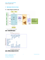
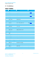
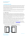
Class 1 Bluetooth v2.0 Module HARDWARE INTEGRATION GUIDE VERSION 1.4 Part # BT730-SA, BT730-SC Americas: +1-800-492-2320 Option 2 Europe: +44-1628-858-940 Hong Kong: +852-2923-0610 www.lairdtech.com/bluetooth Class 1 Bluetooth v2.0 Module Hardware Integration Guide REVISION HISTORY Revision Revision Date Description 1.0 19 June 2013 Initial Release 1.1 23 June 2013 Replaced “PCB Land Pattern and Antenna Keep-out for BT730-SA” image Fixed incorrect text Updated table captions 1.2 30 August 2013 1.3 30 September 2013 1.4 06 Feb 2014 Americas: +1-800-492-2320 Option 2 Europe: +44-1628-858-940 Hong Kong: +852-2923-0610 www.lairdtech.com/bluetooth Removal of OBEX Client Updated Bluetooth SIG Approvals Updated BT730-SA placement on host PCB image Updated Bluetooth SIG Qualification section 2 CONN-HIG-BT730_1 Class 1 Bluetooth v2.0 Module Hardware Integration Guide CONTENTS Revision History ............................................................................................................................................ 2 Contents ........................................................................................................................................................ 3 Overview and Key Features ......................................................................................................................... 4 Features & Benefits.................................................................................................................................................4 1 Specifications ......................................................................................................................................... 5 1.1 Detailed Specifications ..................................................................................................................................5 2 Hardware Specifications ........................................................................................................................ 7 2.1 Block Diagram and Pin-out ............................................................................................................................7 2.2 Pin Definitions ................................................................................................................................................8 2.3 Electrical Specifications ...............................................................................................................................10 3 IO Characteristics ................................................................................................................................. 12 3.1 Power Consumption ....................................................................................................................................12 3.2 Typical Current Consumption in mA ............................................................................................................12 4 Functional Description ........................................................................................................................ 13 4.1 UART Interface .............................................................................................................................................13 4.2 SPI Bus .........................................................................................................................................................14 4.3 PCM Interface ..............................................................................................................................................14 4.4 General Purpose I/O and ADC .....................................................................................................................14 4.5 BT730-SA On-board Chip Antenna Characteristics ......................................................................................15 5 Hardware Integration Suggestions .................................................................................................... 16 5.1 Circuit ...........................................................................................................................................................16 5.2 PCB Layout on Host PCB - General...............................................................................................................16 5.3 PCB Layout on Host PCB for BT730-SA ........................................................................................................17 5.4 External Antenna Integration with BT730-SC ..............................................................................................19 6 Mechanical Details ............................................................................................................................... 20 6.1 BT730-SC Mechanical Details ......................................................................................................................20 6.2 BT730-SA Mechanical Details ......................................................................................................................20 6.3 BT730 Pad Definitions – Mechanical Drawing .............................................................................................21 6.4 PCB Land Pattern and Antenna Keep-out for BT730-SA ..............................................................................22 7 Application Note for Surface Mount Modules .................................................................................. 23 7.1 Introduction .................................................................................................................................................23 7.2 Shipping .......................................................................................................................................................23 7.3 Reflow Parameters ......................................................................................................................................24 8 Regulatory Statements ........................................................................................................................ 25 8.1 FCC ...............................................................................................................................................................25 8.2 Power Exposure Information .......................................................................................................................25 8.3 OEM Responsibilities ...................................................................................................................................26 8.4 Industry Canada (IC) Warning: .....................................................................................................................27 8.5 CE Regulatory ...............................................................................................................................................28 9 EU Declarations of Conformity ........................................................................................................... 29 9.1 BT730-SA......................................................................................................................................................29 9.2 BT730-SC ......................................................................................................................................................30 10 Bluetooth SIG Qualification ................................................................................................................ 31 10.1 Additional Assistance ...................................................................................................................................31 11 Ordering Information .......................................................................................................................... 32 11.1 General Comments ......................................................................................................................................32 Americas: +1-800-492-2320 Option 2 Europe: +44-1628-858-940 Hong Kong: +852-2923-0610 www.lairdtech.com/bluetooth 3 CONN-HIG-BT730_1 Class 1 Bluetooth v2.0 Module Hardware Integration Guide OVERVIEW AND KEY FEATURES Every BT730 series Bluetooth® module from Laird Technologies is designed to add robust, long-range Bluetooth data connectivity to any device. Based on the market-leading Cambridge Silicon Radio (CSR) BC04 chipset, BT730 modules provide exceptionally low power consumption with outstanding Class 1 range via 18 dBm of transmit power. A broad range of Bluetooth profiles and other vital features make BT730 modules superior to other Bluetooth modules. With a compact footprint of 15.29 x 28.71 mm, the modules deliver maximum range with minimum size. Another integration advantage is the inclusion of a complete Bluetooth v2.0 protocol stack with support for multi-point connections and numerous Bluetooth profiles including Serial Port Profile (SPP), Dial Up Networking (DUN), FTP Client plus partial support for Headset (HSP) and HandsFree (HFP). BT730 modules are fully qualified as Bluetooth end products, enabling designers to integrate the modules in devices without the need for further Bluetooth qualification. An integrated AT command processor interfaces to the host system over a serial port using an extensive range of AT commands. The AT command set abstracts the Bluetooth protocol from the host application, saving many months of programming and integration time. It provides extremely short integration times for data oriented Bluetooth applications. The included firmware provides programming support for multi-point applications that use up to three simultaneous data connections to and from the robust BT730 module. A low-cost developer’s kit makes it easy for an OEM to integrate the module and guarantees the fastest route to prototype and then mass production. Features & Benefits Bluetooth v2.0 External or internal antennas Comprehensive AT command set Bluetooth EPL Compact footprint Class 1 output - 18dBm UART interface with GPIO, PCM, and ADC lines Industrial temperature range Field proven firmware used on BTM40x and BISM II product ranges Application Areas Bluetooth Profiles Support Americas: +1-800-492-2320 Option 2 Europe: +44-1628-858-940 Hong Kong: +852-2923-0610 www.lairdtech.com/bluetooth Medical devices ePOS terminals Automotive diagnostic equipment Barcode scanners Industrial cable replacement Serial Port Profile (SPP) Dial Up Networking (DUN) FTP Client partial support for Headset (HSP) and Hands Free (HFP) 4 CONN-HIG-BT730_1 Class 1 Bluetooth v2.0 Module Hardware Integration Guide 1 SPECIFICATIONS 1.1 Detailed Specifications Table 2.2.1.1: Detailed specifications Categories Wireless Specification Feature Bluetooth® Frequency Bluetooth Transmitter Class Max Transmit Power Implementation V2.0 2.402 - 2.480 GHz Class 1 (Basic Rate BT) 18 dBm into integrated antenna (BT730-SA) 16 dBm into UFL antenna connector (BT730-SC) -9 dBm into integrated antenna -9 dBm into UFL antenna connector Better than -87 dBm (at 25°C) Up to 1000m (Line of Sight) Up to 1.0 Mbps (over the air) Circa 300 kbps One UART TX, RX, DCD, RI, DTR, DSR, CTS, RTS1 Default 9600, n,8, 1 From 1,200 to 921,600 bps 8 configurable lines Two ADC channels, 8 bit resolution One PCM interface – see Audio section PCM_CLK, PCM_IN, PCM_SYNC, PCM_OUT Serial Port Profile Dial Up Networking File Transfer Client Profile Hands Free & Headset AT Command Set Multi-Point API - 3 simultaneous connections Min Transmit Power Host Interface Receive Sensitivity Range Data Rates UART Data Transfer Rate UART GPIO ADC PCM Profiles Command Interfaces SPP DUN FTP Client HFP & HSP (Audio Gateway) Operation Modes Firmware Upgrade Firmware Upgrade over UART Audio Support SCO Channels PCM Interface Supply Voltage Supply 3 x PCM Channels @ 64 kpbs SCO and eSCO Configurable as master or slave 8 bit A-law 8 bit µ-law 13 bit linear PCM Clock available when in slave mode 3.3 – 5.0 V On-board regulators and brown-out detection. GPIO voltages are 3.3V logic. Americas: +1-800-492-2320 Option 2 Europe: +44-1628-858-940 Hong Kong: +852-2923-0610 www.lairdtech.com/bluetooth 5 CONN-HIG-BT730_1 Class 1 Bluetooth v2.0 Module Hardware Integration Guide Categories Power Consumption Feature Various Modes – Typical values (see Power Consumption section for test conditions) Antenna Options Internal External Connections Dimensions Weight Operating Storage Lead Free Warranty Development Kit Bluetooth® FCC / IC / CE Physical Environmental Miscellaneous Development Tools Approvals Implementation Idle mode 1.25 mA Discoverable 2.7 mA to 55 mA Inquiry mode 65 mA Connecting mode 66 mA Connected mode 6 mA (no data transfer) Connected mode 35 mA (max data transfer) Sniff mode 1.8 mA Multilayer ceramic chip - BT730-SA Connection via u.FL - BT730-SC Surface Mount Pads (1.2mm pitch) 15.29 mm x 28.71 mm x 2.5 mm 1.5 g -40°C to +85°C -40°C to +85°C Lead-free and RoHS compliant 5-Year Limited Lifetime Development kit DVK-BT730 and software tools End Product Listing (EPL) All BT730 Series 1. DSR, DTR, RI and DCD are configurable either as GPIO or as modem control lines. Americas: +1-800-492-2320 Option 2 Europe: +44-1628-858-940 Hong Kong: +852-2923-0610 www.lairdtech.com/bluetooth 6 CONN-HIG-BT730_1 Class 1 Bluetooth v2.0 Module Hardware Integration Guide 2 HARDWARE SPECIFICATIONS 2.1 Block Diagram and Pin-out Ceramic Chip Antenna OR UFL RF connector Figure 1: Functional Block Diagram Figure 2: BT730-Sx module pin-out (Top View) Americas: +1-800-492-2320 Option 2 Europe: +44-1628-858-940 Hong Kong: +852-2923-0610 www.lairdtech.com/bluetooth 7 CONN-HIG-BT730_1 Class 1 Bluetooth v2.0 Module Hardware Integration Guide 2.2 Pin Definitions Table 2.2.1.1: Pin definitions Pin Signal Description Comment 1 GND 2 SPI_MOSI SPI bus serial I/P See Note 2 3 GPIO6 I/O for host 4 GPIO7 I/O for host 5 nRESET Module reset I/P See Note 3 6 SPI_CLK SPI bus clock I/P See Note 2 7 PCM_CLK PCM clock I/P 8 PCM_SYNC PCM sync I/P 9 PCM_IN PCM data I/P 10 PCM_OUT PCM Data O/P 11 VCC_IN 3.3 V < VCC_IN < 5.0 V See Note 4 12 GND 13 VCC_3V3_monitor 3.3 V Monitor (do not connect) See Note 5 14 Analogue 1 1.8 V max 15 GND 16 UART_DSR UART_DSR I/P 17 UART_DCD UART_DCD I/P or O/ P 18 GPIO_9 I/O for host 19 GPIO_8 I/O for host 20 GND 21 Analogue 0 1.8 V max 22 UART_RX Receive data I/P 23 UART_TX Transmit data O/P 24 UART_RTS Request to Send O/P 25 UART_CTS Clear to Send I/P 26 NC (Reserved USB_D+) Not used for AT module variants 27 NC (Reserved USB_D-) Not used for AT module variants 28 UART_RI Ring Input or Output 29 GPIO_3/UART_DTR I/O for host/UART_DTR 30 GPIO_5 I/O for host 31 GPIO_4 I/O for host 32 SPI_CSB SPI bus chip select I/P See Note 2 33 SPI_MISO SPI bus serial O/P See Note 2 Americas: +1-800-492-2320 Option 2 Europe: +44-1628-858-940 Hong Kong: +852-2923-0610 www.lairdtech.com/bluetooth 8 CONN-HIG-BT730_1 Class 1 Bluetooth v2.0 Module Hardware Integration Guide Notes: 1. Unused pins may have internal connections and must not be connected. 2. Pins 2, 6, 32, and 33 (SPI related) are only for Laird internal production purposes. 3. Power-on-reset (power cycling and brown out consideration) – The reset circuitry within the BT730 module incorporates a brown-out detector; this may simplify power supply design. The BT730 reset line is an active low input (Input debounced so must be low for more than 5 ms to cause a reset). Upon the application of power, the Power On Reset circuit built into the module ensures that the unit starts correctly. There is no need for an external power reset monitor. 4. Power Supply Consideration – The power supply for the module should be a single voltage source of VCC within the VCC_IN range of 3.3 V to 5.0 V. It must be able to provide sufficient current in a transmit burst. This can rise to 200 mA. To limit dissipation it is recommended that you use a voltage at the lower end of the range. 5. The module includes regulators to provide internal local 3.3 V. This rail is accessible on pin 13 for monitoring purposes only. Under no circumstances should this pin be used to source current. 2.2.1 COMPATIBILITY NOTE FOR LEGACY DEVICES If Reset compatibility is required with BTM402 and BTM404: Reset logic must be inverted (on the host PCB), by using suitable BJT (MMBT3904) with collector connected to Reset pin BT730 module pin 5. A fixed 10k Ohm pull down resistor to ground (BJT input) then ensures that the BT730 module is out of reset for the condition when host has yet to control the reset line. Add a 10 k pull-up to the host PCB on the UART_RX, otherwise the module will remain in deep sleep if not driven to high. Add a 10 k pull-down to the host PCB on the UART_CTS that if it is not connected (which we do not recommend) then the default state for UART_CTS input will be asserted which means can send data out of UART_TX line. GPIO lines can be configured through software to be either inputs or outputs with weak or strong pullups or pull-downs. At reset, all GPIO lines are configured as inputs with weak pull-downs. UART_RX, UART_TX, UART_CTS, UART_RTS, UART_RI, UART_DCD, and UART_DSR are 3.3 V level logic. For example, when RX and TX are idle they sit at 3.3 V. Conversely, for handshaking pins CTS, RTS, RI, DCD, and DSR, a 0 V is treated as an assertion. Pin 28 (UART_RI) is active low. It is normally 3.3 V. When a remote device initiates a connection, this pin goes low. This means that when this pin is converted to RS232 voltage levels it has the correct voltage level for assertion. Pin 17 (UART_DCD) is active low. It is normally 3.3 V. When a connection is live, this pin is low. This means that when this pin is converted to RS232 voltage levels it has the correct voltage level for assertion. Pin 16 (UART_DSR) is an input, with active low logic. It should be connected to the DTR output of the host. When the BTM730 module is in high speed mode (see S Register 507 in the Firmware User manual), this pin should be asserted by the host to ensure that the connection is maintained. A deassertion means that the connection should be dropped or an online command mode is being requested. Pin 13 (VCC_3V3 monitor) may only be used for monitoring purposes. It must not be used as a current source. Americas: +1-800-492-2320 Option 2 Europe: +44-1628-858-940 Hong Kong: +852-2923-0610 www.lairdtech.com/bluetooth 9 CONN-HIG-BT730_1 Class 1 Bluetooth v2.0 Module Hardware Integration Guide The GPIO pins can be accessed using S Registers 623 to 629. GPIO3 is also used for DTR output (active low). See S Register 552 and 553 in the Firmware User manual. Analogue 0 and 1 should not exceed 1.8 V and S Registers 701 and 702 are used to access them. 2.3 Electrical Specifications 2.3.1 Absolute Maximum ratings Absolute maximum ratings for supply voltage and voltages on digital and analogue pins of the module are listed below; exceeding these values will cause permanent damage. Table 2.3.1.1: Absolute Maximum Ratings Parameter Min Max Unit Peak current of power supply 0 200 mA Voltage at digital pins -0.4 3.7 V Voltage at POWER pin 2.9 6.0 V 2.3.2 Recommended Operating Parameters Table 2.3.2.1: Power Supply Signal Name VCC_IN GND I/O Voltage level 11 I 3.3 V to 5.0 V * Typ 3.5 V 13 Comments Ityp = 115 mA Four (4) ground terminals to be attached in parallel. 1, 12, 15, 20 VCC_3V3_monitor Note: Pin No O 3.3 V typical For monitoring only. No current source. VCC_3V3_monitor refers to internal voltage generated by the LDO inside the module which is typically 3.3 V. So to achieve 3.3 V for VCC_3V3_monitor (at Max Tx Power) requires VCC_IN of 3.5 V. IO voltage levels follows VCC_3V3_monitor. At minimum VCC_VIN of 3.3 V, the internal LDO generates 3.3 V but when Radio Tx at max Tx power, VCC_3V3_monitor drops a little (to ~3.15 V). Table 2.3.2.2: Signal Levels for Interface, PCM, SPI, and GPIO Signal Type Signal level Input VILmin= -0.4 V VILmax=0.8 V VIHmin=2.3 V VIHmax=3.7 V Output Americas: +1-800-492-2320 Option 2 Europe: +44-1628-858-940 Hong Kong: +852-2923-0610 www.lairdtech.com/bluetooth Signal level @ 0 mA load VOLmax=0.2 V VOHmin=3.1 V 10 CONN-HIG-BT730_1 Class 1 Bluetooth v2.0 Module Hardware Integration Guide Table 2.3.2.3: UART Interface Signal Name UART_TX UART_RX UART_CTS UART_RTS UART_DSR UART_DTR UART_RI UART_DCD Pin No 23 22 25 24 16 29 28 17 I/O O I I O I O I or O I or O Comments Pin No 2 33 32 6 I/O I O I I Comments I/O I or O I I or O O Comments Shared with GPIO3 Direction may be programmed. Direction may be programmed. Table 2.3.2.4: SPI Bus Signal Name SPI_MOSI SPI_MISO SPI_CSB SPI_CLK Laird INTERNAL USE ONLY - Used to reprogram Flash in Laird production. Table 2.3.2.5: PCM Interface Signal Name PCM_CLK PCM_IN PCM_SYNC PCM_OUT Pin No 7 9 8 10 If unused keep pins open. PCM output signals are tri-stated when there is not an active SCO or eSCO connection. Table 2.3.2.6: General Purpose I/O and ADC Signal Name GPIO_3 - 9 Analogue0, Analogue1 Pin No 3, 4, 16, 17, 18, 19, 29, 30, 31 14, 21 I/O I or O Signal level See 3.3.2.2 Comments I Range 0 – 1.8 V 8 bit Table 2.3.2.7: Miscellaneous Signal Name nRESET Pin No 5 I/O I Signal level VILmax=1.0V VIHmin=2.3V Americas: +1-800-492-2320 Option 2 Europe: +44-1628-858-940 Hong Kong: +852-2923-0610 www.lairdtech.com/bluetooth 11 Comments Active LOW. The Reset input contains a 10 kΩ pull-up resistor (internal to module). CONN-HIG-BT730_1 Class 1 Bluetooth v2.0 Module Hardware Integration Guide 3 IO CHARACTERISTICS 3.1 Power Consumption The current drain from the VCC power input line is dependent on various factors. The three most significant factors are the voltage level at VCC, UART baud rate, and the operating mode. The hardware specification for the module allows for a voltage range of 3.3 to 5.0 at VCC. The unit includes a linear regulator and tests have shown that there is no significant difference in current draw when VCC changes within the operating limits. Tests have shown that where power dissipation is an issue, it is best to keep VCC at the lower end of the range. The UART baud rate has a bearing on power dissipation because, as is normal for digital electronics, the power requirements increase linearly with increasing clocking frequencies. Because of this, higher baud rates result in a higher current drain. Finally, the significant operating modes are: idle, waiting for a connection, inquiring, initiating a connection, sniff, and connected. With connected mode, it is also relevant to differentiate between no data being transferred and when data is being transferred at the maximum rate possible. The AT command set document describes how to configure the module for optimal power performance. 3.2 Typical Current Consumption in mA Table 4-2: Current Consumption VCC_IN = 3.8 V, Baudrate = 9600 bps Typical Average Current (mA) Separation Distance = 15 meters Idle Mode, S512=1 1.25 mA Wait for Connection Or Discoverable Mode, 55 mA AT+BTP S508=S510=640, S509=S511=320 Wait for Connection Or Discoverable Mode, 2.7 mA AT+BTP S508=S510=1000, S509=S511=11 Inquiry Mode, AT+BTI 65 mA Connecting Mode (ATDxxx) 66 mA Connected Mode (No Data Transfer) 6 mA Connected Mode (Max Data Transfer) 35 mA Sniff Mode 1.8 mA S564=1000, S563=500, S562=50, S561=10 Americas: +1-800-492-2320 Option 2 Europe: +44-1628-858-940 Hong Kong: +852-2923-0610 www.lairdtech.com/bluetooth 12 CONN-HIG-BT730_1 Class 1 Bluetooth v2.0 Module Hardware Integration Guide 4 FUNCTIONAL DESCRIPTION The BT730 Bluetooth module is a self-contained Bluetooth product and requires only power to implement full Bluetooth communication. The integrated, high performance antenna, together with the RF and base-band circuitry, provides the Bluetooth wireless link; the UART interface provides a connection to the host system. The variety of interfaces and the AT command set allow the BT730 module to be used for a wide variety of long range wireless applications, from simple cable replacement to complex multipoint applications, where multiple radio links are active at the same time. The complexity and flexibility of configuration are made simple for the design engineer by the integration of a comprehensive set of AT commands, supplemented with a range of “S” registers which are used for nonvolatile storage of system parameters. To provide the widest scope for integration, a range of different physical host interfaces are provided. 4.1 UART Interface UART_TX, UART_RX, UART_RTS, and UART_CTS form a conventional asynchronous serial data port with handshaking. The interface is designed to operate correctly when connected to other UART devices such as the 16550A. The signalling levels are nominal 0 V and 3.3 V and are inverted with respect to the signalling on an RS232 cable. The interface is programmable over a variety of bitrates; no, even, or odd parity; stop bit and hardware flow control. The default condition on power-up is pre-assigned in the external flash. Two-way hardware flow control is implemented by UART_RTS and UART_CTS. UART_RTS is an output and is active low. UART_CTS is an input and is active low. These signals operate according to normal industry convention. UART_RX, UART_TX, UART_CTS, UART_RTS, UART_RI, UART_DCD, and UART_DSR are all 3.3 V level logic. For example, when RX and TX are idle, they sit at 3.3 V. Conversely for handshaking pins CTS, RTS, RI, DCD, and DSR, a 0 V is treated as an assertion. By writing different values to the relevant S register, the UART_RI can be continuously polled to detect incoming communication. The UART_RI signal serves to indicate incoming calls. UART_DSR is an active low input. It should be connected to DTR output of the host. When the module is running in high speed mode (see definition for S Reg 507 in the Firmware User manual), this pin should be asserted by the host to ensure connection is maintained. A de-assertion means that the connection should be dropped or an online command mode is being requested. The module communicates with the customer application using the following signals: Port /TXD of the application sends data to the module’s UART_RX signal line Port /RXD of the application receives data from the module’s UART_TX signal line BT730 Application - Host UART_TX /RXD UART_RX /TXD UART_CTS /RTS UART_RTS /CTS UART_DSR /DTR UART_DTR /DSR UART_RI /RING UART_DCD /DCD Americas: +1-800-492-2320 Option 2 Europe: +44-1628-858-940 Hong Kong: +852-2923-0610 www.lairdtech.com/bluetooth 13 CONN-HIG-BT730_1 Class 1 Bluetooth v2.0 Module Hardware Integration Guide Note: The serial module output is at 3.3 V CMOS logic levels. Level conversion must be added to interface with an RS-232 level compliant interface. Some serial implementations link CTS and RTS to remove the need for handshaking. Laird does not recommend linking CTS and RTS other than for testing and prototyping. If these pins are linked and the host sends data at the point that the BT730 deasserts its RTS signal, then there is a significant risk that internal receive buffers will overflow; this could lead to an internal processor crash. This also leads to a drop in connection and may require a power cycle to reset the module. Laird recommends that the correct CTS/RTS handshaking protocol be followed for proper operation. 4.2 SPI Bus The module is a slave device that uses terminals SPI_MOSI, SPI_MISO, SPI_CLK, and SPI_CSB. This interface is used for program firmware updates ONLY at the factory. Laird supplies a PC-based utility to allow a firmware upgrade over the UART port. It is highly recommended that customers use the UART method for updating firmware. Note: The designer should be aware that no security protection is built into the hardware or firmware associated with this port, so the terminals should not be permanently connected in a PC application. 4.3 PCM Interface PCM_OUT, PCM_IN, PCM_CLK, and PCM_SYNC carry up to three bi-directional channels of voice data, each at 8 k samples/s. The format of the PCM samples can be 8-bit A-law, 8-bit μ-law, 13-bit linear, or16-bit linear. The PCM_CLK and PCM_SYNC terminals can be configured as inputs or outputs, depending on whether the module is the master or slave of the PCM interface. Please contact a Laird FAE for further details. The module is compatible with the Motorola SSI TM interface and interfaces directly to PCM audio codec chips including the following: 4.3.1 Compatible Codec Chips OKI 7702 single channel A-law and μ-law CODEC Winbond W681360 13 bit linear CODEC 4.4 General Purpose I/O and ADC 4.4.1 GPIO Seven lines of programmable bi-directional input/outputs (I/O) are provided that can be accessed either via the UART port or Over-the-Air (OTA) from a second Bluetooth unit. These can be used as data inputs or to control external equipment. By using these in OTA mode, a BT730 module can be used for control and data acquisition without the need for any additional host processor. Each of the GPIO[3:9] ports can be independently configured to be either an input or output. A selection of ports can be accessed synchronously. The ports are powered from internal VCC_3V3. The mode of these lines can be configured and the lines are accessed via S Registers 623 to 629. Americas: +1-800-492-2320 Option 2 Europe: +44-1628-858-940 Hong Kong: +852-2923-0610 www.lairdtech.com/bluetooth 14 CONN-HIG-BT730_1 Class 1 Bluetooth v2.0 Module Hardware Integration Guide 4.4.2 ADC The BT730 provides access to two 8-bit ADCs (Analogue 0 and 1). These provide an input range of 0 mV to 1,800 mV, which can be read using the S registers 701 and 702. Suitable external scaling and over-voltage protection should be incorporated in your design. The module provides five samples per second at the UART with a baud rate of 115,200 or above. 4.5 BT730-SA On-board Chip Antenna Characteristics The BT730-SA on-board chip monopole antenna radiated performance depends on the host PCB layout. BT730 carrier board was used for BT730-SA development and antenna performance evaluation. To obtain similar performance, follow the guidelines in PCB Layout on Host PCB for BT730-SA to allow the on-board antenna to radiate and reduce proximity effects due to nearby host PCB GND copper or metal covers. BT730-SA on-board antenna datasheet can be accessed from the following link: http://www.acxc.com.tw/product/at3216/AT3216-B2R7HAA_071204.pdf Americas: +1-800-492-2320 Option 2 Europe: +44-1628-858-940 Hong Kong: +852-2923-0610 www.lairdtech.com/bluetooth 15 CONN-HIG-BT730_1 Class 1 Bluetooth v2.0 Module Hardware Integration Guide 5 HARDWARE INTEGRATION SUGGESTIONS 5.1 Circuit The BT730 series module is easy to integrate requiring no external components on the customer’s board apart from those required by customer for development and in customers end application. Checklist (for the schematic): VCC_IN: External power source within the operating range specification of BT730-Sx. Add decoupling (or bulk) capacitors for filtering (or reservoir) the external source. Power-on reset circuitry within BT730Sx series module incorporates brown-out detector, thus simplifying power supply design. Upon application of power, the internal power-on reset ensures module starts correctly. AIN (ADC) and GPIO (or UART) pin IO voltage levels: BT73-Sx GPIO voltage levels are at VCC_3V3_monitor pin (see section 2.3). Ensure input voltage levels into GPIO pins are at VCC_3V3 _monitor voltage levels. Ensure ADC pin maximum input voltage (1.8 V) for damage is not violated. UART: Is required. Add connector to allow UART to be interfaced to PC (via UART –RS232 or UARTUSB). UART_RX and UART_CTS: Add a 10 k pull-up to the host PCB on the UART_RX, otherwise the module remains in deep sleep if not driven to high. The pull-up prevents the module from going into deep sleep when UART_RX line is idling. Add a 10 k pull-down to the host PCB on the UART_CTS that, if it is not connected (which we do not recommend) then the default state for UART_CTS input will be asserted which means can send data out of UART_TX line. nRESET pin (active low): Hardware reset. Wire out to push button or drive by host. If used external reset must be exerted for a minimum of 5 mS. By default, the module is out of reset when power is applied to the VCC pin. PCM: All four PCM signals are routed directly from chipset to external BT730-Sx module pins. It is then up to customer to configure appropriately. A 4.7 k pull down resistor to ground on PCM_OUT may help resolve audio noise problems when chipset PCM_OUT line tristates. 5.2 PCB Layout on Host PCB - General Checklist (for PCB): MUST locate the BT730-SA module close to the edge of PCB (mandatory for BT730-SA for on-board chips antenna to radiate properly). Use solid GND plane on inner layer (for best EMC and RF performance). Place GND vias as close to module GND pads as possible. Unused host PCB area on surface layer can be flooded with copper but place GND vias regularly to connect copper flood to inner GND plane. If GND flood copper underside the module then connect with GND vias to inner GND plane. Route traces to avoid noise being picked up on VCC_IN supply, Analogue and GPIO (digital) traces. Ensure there is no exposed copper on the underside of the module (refer to land pattern drawing of BT730-Sx). Americas: +1-800-492-2320 Option 2 Europe: +44-1628-858-940 Hong Kong: +852-2923-0610 www.lairdtech.com/bluetooth 16 CONN-HIG-BT730_1 Class 1 Bluetooth v2.0 Module Hardware Integration Guide 5.3 PCB Layout on Host PCB for BT730-SA 5.3.1 Antenna keep-out on host PCB The BT730-SA has an integrated chip antenna and its performance is sensitive to the host PCB. It is critical to locate the BT730-SA on the edge of the host PCB (or corner) to allow the antenna to radiate properly. Refer to guidelines in the section PCB Land Pattern and Antenna Keep-out area for BT730-SA. Some of the guidelines are repeated below. Ensure there is no copper in the antenna keep-out area on any layers of the host PCB. Keep all mounting hardware and metal clear of the area to allow proper antenna radiation. For best antenna performance, place the BT730-SA module on the edge of the host PCB, preferably in the corner with the antenna facing the corner. An example shown in Figure 3. A different host PCB thickness dielectric will have small effect on antenna (the BT730 carrier development board (used for antenna performance evaluation) thickness was 0.78 mm). The antenna-keep-out defined in PCB Land Pattern and Antenna Keep-out area for BT730-SA applies when the BT730-SA is placed in the corner of the host PCB. When BT730-SA cannot be placed as such, it must be placed on the edge of the host PCB and a modified antenna keep out must be observed. This antenna keep-out modification is shown in Figure 4 (antenna keep-out is extended by 8 mm on both sides). Figure 3: BT730-SA placement in the corner of host PCB. Figure 4: BT730-SA placement in the edge (not corner) of host PCB (with modified antenna keep-out). Americas: +1-800-492-2320 Option 2 Europe: +44-1628-858-940 Hong Kong: +852-2923-0610 www.lairdtech.com/bluetooth 17 CONN-HIG-BT730_1 Class 1 Bluetooth v2.0 Module Hardware Integration Guide Note: Copper cut-away on all layers in “antenna keep-out” area under BT730-SA module on host PCB. Refer to “antenna keep-out” defined in section 6.4 PCB Land Pattern and Antenna Keep-out for BT730-SA. 5.3.2 Antenna Keep-out and Proximity to Metal or Plastic Checklist (for metal /plastic enclosure): Figure 12A and 12B shows recommended and not recommended locations for metal with respect to a BT730-SA module on-board antenna. Minimum safe distance for metals without seriously compromising the antenna (tuning) is 40 mm top/bottom and 30 mm left or right. Metal close to the BT730-SA chip monopole antenna (bottom, top, left, right, any direction) will have degradation on the antenna performance. The amount of degradation is entirely system dependent which means some testing by customer is required (in their host application). Anything metal closer than 20 mm starts to significantly degrade performance (S11, gain, radiation efficiency). It is best that the customer tests the range with a mock-up (or actual prototype) of the product to assess effects of enclosure height (and material, whether metal or plastic). Figure 5: Recommended BT730-SA placement on host PCB and proximity to metal cover Figure 6: Not recommended BT730-SA placement on host PCB and proximity to metal cover Americas: +1-800-492-2320 Option 2 Europe: +44-1628-858-940 Hong Kong: +852-2923-0610 www.lairdtech.com/bluetooth 18 CONN-HIG-BT730_1 Class 1 Bluetooth v2.0 Module Hardware Integration Guide 5.4 External Antenna Integration with BT730-SC Refer to the regulatory sections for FCC, IC, and CE, for details of use of BT730-SC with external antennas in each regulatory region. The BT730-SC family has been designed to operate with the antennas listed below with a maximum gain of 2 dBi. The required antenna impedance is 50 ohms. External antennas improve radiation efficiency. Item Part Number Mfg. Type Gain (dBi) Connector Type 1 MAF94045 Laird Internal 2 UFL 2 WRR2400- IP04-B(MAF94019) Laird Dipole 1.5 UFL 3 WTC2450-IP04-K(MAF94006) Laird Dipole 2 UFL 4 S181FL-L-RMM-2450S Nearson (Laird) Dipole 2 UFL Note 1: Integral RF co-axial cable with UFL connector. Antenna manufacturer Laird contact information: Email: [email protected] Americas: +1-800-492-2320 Option 2 Europe: +44-1628-858-940 Hong Kong: +852-2923-0610 www.lairdtech.com/bluetooth 19 CONN-HIG-BT730_1 Class 1 Bluetooth v2.0 Module Hardware Integration Guide 6 MECHANICAL DETAILS 6.1 BT730-SC Mechanical Details Figure 7: BT730-SC mechanical details 6.2 BT730-SA Mechanical Details Figure 8: BT730-SA mechanical details Americas: +1-800-492-2320 Option 2 Europe: +44-1628-858-940 Hong Kong: +852-2923-0610 www.lairdtech.com/bluetooth 20 CONN-HIG-BT730_1 Class 1 Bluetooth v2.0 Module Hardware Integration Guide 6.3 BT730 Pad Definitions – Mechanical Drawing Figure 9: BT7xx Mechanical Drawing Americas: +1-800-492-2320 Option 2 Europe: +44-1628-858-940 Hong Kong: +852-2923-0610 www.lairdtech.com/bluetooth 21 CONN-HIG-BT730_1 Class 1 Bluetooth v2.0 Module Hardware Integration Guide 6.4 PCB Land Pattern and Antenna Keep-out for BT730-SA Unit is mm. Figure 10: PCB Land Pattern and Antenna Keep-out for BT730-SA APPLICATION NOTES 1. Ensure there is no copper in the antenna ‘keep out area’ on any layers of the host PCB. Also keep all mounting hardware or any metal clear of the area to reduce effects of proximity detuning the antenna and to help antenna radiate properly. Refer to section 5.3.2 for more information. 2. For BT730-SA (with on-board chip antenna) best antenna performance, the module BT730-SA must be placed on the edge of the host PCB and preferably in the corner with the antenna facing the corner (see Figure 3 in section 5.3.1). The module is placed in the corner of host PCB above the keepout area. If the BT730-SA is not placed in corner but on edge of host PCB, the antenna keep-out area must be modified (see Figure 4 in section 5.3.1). 3. Ensure that there is no exposed copper under the module on the host PCB. 4. The user may modify the PCB land pattern dimensions based on their experience and capability. Americas: +1-800-492-2320 Option 2 Europe: +44-1628-858-940 Hong Kong: +852-2923-0610 www.lairdtech.com/bluetooth 22 CONN-HIG-BT730_1 Class 1 Bluetooth v2.0 Module Hardware Integration Guide 7 APPLICATION NOTE FOR SURFACE MOUNT MODULES 7.1 Introduction Laird surface mount modules are designed to conform to all major manufacturing guidelines. This application note is intended to provide additional guidance beyond the information that is presented in the user manual. This application note is considered a living document and will be updated as new information is presented. The modules are designed to meet the needs of a number of commercial and industrial applications. The modules are designed to be easily manufactured and conform to current automated manufacturing processes. 7.2 Shipping Modules are shipped in ESD (Electrostatic Discharge) safe trays that can be loaded into most manufacturers pick and place machines. Layouts of the trays are provided in Figure 11. Figure 11: BT730 shipping tray details Americas: +1-800-492-2320 Option 2 Europe: +44-1628-858-940 Hong Kong: +852-2923-0610 www.lairdtech.com/bluetooth 23 CONN-HIG-BT730_1 Class 1 Bluetooth v2.0 Module Hardware Integration Guide 7.3 Reflow Parameters Laird surface mount modules are designed to be easily manufactured including reflow soldering to a PCB. It is ultimately the responsibility of the customer to choose the appropriate solder paste and to ensure oven temperatures during reflow meet the requirements of the solder paste. Laird Technologies’ surface mount modules conform to J-STD-020D1 standards for reflow temperatures. Important: During reflow, modules should not be above 260° and not for more than 30 seconds. Figure 12: Recommended reflow temperature Temperatures should not exceed the minimums or maximums presented in Table 5.3.2.1. Table 5.3.2.1: Recommended Maximum and minimum temperatures Specification Value Unit Temperature Inc./Dec. Rate (max) 1~3 °C / Sec Temperature Decrease rate (goal) 2-4 °C / Sec Soak Temp Increase rate (goal) .5 - 1 °C / Sec Flux Soak Period (Min) 70 Sec Flux Soak Period (Max) 120 Sec Flux Soak Temp (Min) 150 °C Flux Soak Temp (max) 190 °C Time Above Liquidous (max) 70 Sec Time Above Liquidous (min) 50 Sec Time In Target Reflow Range (goal) 30 Sec Time At Absolute Peak (max) 5 Sec Liquidous Temperature (SAC305) 218 °C Lower Target Reflow Temperature 240 °C Upper Target Reflow Temperature 250 °C Absolute Peak Temperature 260 °C Americas: +1-800-492-2320 Option 2 Europe: +44-1628-858-940 Hong Kong: +852-2923-0610 www.lairdtech.com/bluetooth 24 CONN-HIG-BT730_1 Class 1 Bluetooth v2.0 Module Hardware Integration Guide 8 REGULATORY STATEMENTS 8.1 FCC Family BT7x0 US/FCC SQGBT700 CANADA/IC 3147A-BT700 PART # FORM FACTOR TX OUTPUT ANTENNA BT730-SA-XX Surface Mount 18 dBm Ceramic BT730-SC-XX Surface Mount 16 dBm U.FL *Last two slots "XX" in Part # are used for production firmware release changes. Can be values 01-99, aa-zz The BT730 family has been designed to operate with the antennas listed below with a maximum gain of 2dBi. The required antenna impedance is 50 ohms. Item 1 2 Mfg. ACX Laird Type Chip Internal 3 Part Number AT3216-B2R7HAAT MAF94045 WRR2400- IP04-B(MAF94019) Laird Dipole 1.5 4 WTC2450-IP04-K(MAF94006) Laird Dipole 2 Nearson (Laird) Dipole 2 5 Note: S181FL-L-RMM-2450S Gain (dBi) 0.5 2 The OEM is free to choose another vendor’s antenna of like type and equal or lesser gain as an antenna appearing in the table and still maintain compliance. Reference FCC Part 15.204(c)(4) for further information on this topic. To reduce potential radio interference to other users, the antenna type and gain should be chosen so that the equivalent isotropic radiated power (EIRP) is not more than that permitted for successful communication. 8.2 Power Exposure Information In general, there are two agency classifications for RF radiation exposure in wireless applications; portable and mobile. Mobile – A mobile device is defined as a transmitting device designed to be used in such a way that a separation distance of at least 20 centimeters is normally maintained between the transmitter's radiating structures and the body of the user or nearby persons. The BT730 is fully modular approved for mobile and fixed applications. Reference FCC Part 2.1091 for further details on mobile devices. This transmitter must not be co-located or operating in conjunction with any other antenna or transmitter. Portable – Portable is a classification of equipment where the user, in general, will be within 20 cm of the transmitting antenna. Portable equipment is further broken down into two classes; within 2.5 cm of human contact and beyond 2.5 cm. The BT730 does not hold a portable approval classification due to its peak output power and modular approval restrictions. Further RF evaluation is required by customers who want to use the BT730 in portable applications. Contact a qualified test house or a Laird Technologies representative for further information on this topic. Reference FCC Part 2.1093 for further details on portable devices. Maximum Permissible Exposure report has been created which shows the minimum distances for Public and Occupational use of the BT730. Americas: +1-800-492-2320 Option 2 Europe: +44-1628-858-940 Hong Kong: +852-2923-0610 www.lairdtech.com/bluetooth 25 CONN-HIG-BT730_1 Class 1 Bluetooth v2.0 Module Hardware Integration Guide Note: Note: Occupational Limit Minimum Distance = 1.5 cm. Public Limit Minimum Distance = 3 cm This equipment was tested and found to comply with the limits for a Class B digital device, pursuant to Part 15 of the FCC Rules. These limits are designed to provide reasonable protection against harmful interference in a residential installation. This equipment generates, uses, and can radiate radio frequency energy and, if not installed and used in accordance with the instructions, may cause harmful interference to radio communications. However, there is no guarantee that interference does not occur in a particular installation. If this equipment does cause harmful interference to radio or television reception, which can be determined by turning the equipment off and on, the user is encouraged to correct the interference by one or more of the following measures: Reorient or relocate the receiving antenna Increase the separation between the equipment and the receiver Connect the equipment to an outlet on a circuit that is different from that to which the receiver is connected. Consult the dealer or an experienced radio/TV technician for help CAUTION: THIS DEVICE COMPLIES WITH PART 15 OF THE FCC RULES AND INDUSTRY CANADA LICENSEEXEMPT RSS STANDARD(S). OPERATION IS SUBJECT TO THE FOLLOWING TWO CONDITIONS: (1) THIS DEVICE MAY NOT CAUSE HARMFUL INTERFERENCE, AND (2) THIS DEVICE MUST ACCEPT ANY INTERFERENCE RECEIVED, INCLUDING INTERFERENCE THAT MAY CAUSE UNDESIRED OPERATION. CAUTION: The OEM should have the device incorporating with the BT740 tested by a qualified test house to verify compliance with FCC Part 15 Subpart B limits for unintentional radiators. CAUTION: Any changes or modifications not expressly approved by Laird could void the user’s authority to operate the equipment. 8.3 OEM Responsibilities This device is intended only for OEM integrators under the following conditions: 1) The antenna must be installed such that 20 cm is maintained between the antenna and users. 2) The transmitter module may not be co-located with any other transmitter or antenna As long as 2 conditions above are met, further transmitter test will not be required. However, the OEM integrator is still responsible for testing their end-product for any additional compliance requirements required with this module installed IMPORTANT NOTE: In the event that these conditions can not be met (for example certain laptop configurations or co-location with another transmitter), then the FCC authorization is no longer considered valid and the FCC ID can not be used on the final product. In these circumstances, the OEM integrator will be responsible for re-evaluating the end product (including the transmitter) and obtaining a separate FCC authorization. End Product Labeling This transmitter module is authorized only for use in device where the antenna may be installed such that 20 cm may be maintained between the antenna and users. The final end product must be labeled in a visible area with the following: “Contains FCC ID: SQGBT700”. Manual Information to the End User The OEM integrator has to be aware not to provide information to the end user regarding how to install or remove this RF module in the user’s manual of the end product which integrates this module. Americas: +1-800-492-2320 Option 2 Europe: +44-1628-858-940 Hong Kong: +852-2923-0610 www.lairdtech.com/bluetooth 26 CONN-HIG-BT730_1 Class 1 Bluetooth v2.0 Module Hardware Integration Guide The end user manual shall include all required regulatory information/warning as show in this manual. 8.4 Industry Canada (IC) Warning: Radiation Exposure Statement: This equipment complies with IC radiation exposure limits set forth for an uncontrolled environment. This equipment should be installed and operated with minimum distance 20cm between the radiator & your body. Déclaration d'exposition aux radiations: Cet équipement est conforme aux limites d'exposition aux rayonnements IC établies pour un environnement non contrôlé. Cet équipement doit être installé et utilisé avec un minimum de 20 cm de distance entre la source de rayonnement et votre corps. This device is intended only for OEM integrators under the following conditions: (For module device use) 1) The antenna must be installed such that 20 cm is maintained between the antenna and users. 2) The transmitter module may not be co-located with any other transmitter or antenna. As long as 2 conditions above are met, further transmitter test will not be required. However, the OEM integrator is still responsible for testing their end-product for any additional compliance requirements required with this module installed. Cet appareil est conçu uniquement pour les intégrateurs OEM dans les conditions suivantes: (Pour utilisation de dispositif module) 1) L'antenne doit être installée de telle sorte qu'une distance de 20 cm est respectée entre l'antenne et les utilisateurs. 2) Le module émetteur peut ne pas être coïmplanté avec un autre émetteur ou antenne. Tant que les 2 conditions ci-dessus sont remplies, des essais supplémentaires sur l'émetteur ne seront pas nécessaires. Toutefois, l'intégrateur OEM est toujours responsable des essais sur son produit final pour toutes exigences de conformité supplémentaires requis pour ce module installé. IMPORTANT NOTE: In the event that these conditions can not be met (for example certain laptop configurations or co-location with another transmitter), then the Canada authorization is no longer considered valid and the IC ID can not be used on the final product. In these circumstances, the OEM integrator will be responsible for re-evaluating the end product (including the transmitter) and obtaining a separate Canada authorization. NOTE IMPORTANTE: Dans le cas où ces conditions ne peuvent être satisfaites (par exemple pour certaines configurations d'ordinateur portable ou de certaines co-localisation avec un autre émetteur), l'autorisation du Canada n'est plus considéré comme valide et l'ID IC ne peut pas être utilisé sur le produit final. Dans ces circonstances, l'intégrateur OEM sera chargé de réévaluer le produit final (y compris l'émetteur) et l'obtention d'une autorisation distincte au Canada. Americas: +1-800-492-2320 Option 2 Europe: +44-1628-858-940 Hong Kong: +852-2923-0610 www.lairdtech.com/bluetooth 27 CONN-HIG-BT730_1 Class 1 Bluetooth v2.0 Module Hardware Integration Guide End Product Labeling This transmitter module is authorized only for use in device where the antenna may be installed such that 20 cm may be maintained between the antenna and users. The final end product must be labeled in a visible area with the following: “Contains IC: ”. Plaque signalétique du produit final Ce module émetteur est autorisé uniquement pour une utilisation dans un dispositif où l'antenne peut être installée de telle sorte qu'une distance de 20cm peut être maintenue entre l'antenne et les utilisateurs. Le produit final doit être étiqueté dans un endroit visible avec l'inscription suivante: "Contient des IC: ". Manual Information To the End User The OEM integrator has to be aware not to provide information to the end user regarding how to install or remove this RF module in the user’s manual of the end product which integrates this module. The end user manual shall include all required regulatory information/warning as show in this manual. Manuel d'information à l'utilisateur final L'intégrateur OEM doit être conscient de ne pas fournir des informations à l'utilisateur final quant à la façon d'installer ou de supprimer ce module RF dans le manuel de l'utilisateur du produit final qui intègre ce module. Le manuel de l'utilisateur final doit inclure toutes les informations réglementaires requises et avertissements comme indiqué dans ce manuel. 8.5 CE Regulatory The BT730 has been tested for compliance with relevant standards for the EU market. The OEM should consult with a qualified test house before entering their device into an EU member country to make sure all regulatory requirements have been met for their complete device. The BT730 was tested with a 2dBi dipole antenna. The OEM is free to use any manufacturer’s antenna and type of antenna but it must be <2dBi to remain in compliance with the Laird reports. Reference the Declaration of Conformities listed below for a full list of the standards that the modules were tested to. Test reports are available upon request. Americas: +1-800-492-2320 Option 2 Europe: +44-1628-858-940 Hong Kong: +852-2923-0610 www.lairdtech.com/bluetooth 28 CONN-HIG-BT730_1 Class 1 Bluetooth v2.0 Module Hardware Integration Guide 9 EU DECLARATIONS OF CONFORMITY 9.1 BT730-SA Manufacturer: Laird Technologies Product: BT730-SA EU Directive: RTTE 1995/5/EC Conformity Assessment: Annex IV Reference standards used for presumption of conformity: Article Number: Requirement Reference standard(s): 3.1a Health and Safety EN 60950-1:2006 3.1b Protection requirements with respect to electromagnetic compatibility EN 301 489-1 V1.8.1 EN 301 489-17 V2.1.1 Emissions: EN55022:2006/A1:2000/A2:2006(ClassB) Immunity: EN61000-4-2:1995/A1:1998/A2:2001 EN61000-4-3:2002/A1:2002 3.2 Means of the efficient use of the EN 300 328 V1.8.1 (2012-06) radio frequency spectrum Declaration: We, Laird Technologies, declare under our sole responsibility that the essential radio test suites have been carried out and that the above product to which this declaration relates is in conformity with all the applicable essential requirements of Article 3 of the EU Directive 1995/5/EC, when used for its intended purpose. Place of Issue: Laird Technologies Saturn House, Mercury Park Wooburn Green HP100HH, United Kingdom tel:+44 (0)1628 858 940 fax: +44 (0)1628 528 382 Date of Issue: June 2013 Name of Authorized Person: Andrew Dobbing, Engineering Manager Signature: Americas: +1-800-492-2320 Option 2 Europe: +44-1628-858-940 Hong Kong: +852-2923-0610 www.lairdtech.com/bluetooth 29 CONN-HIG-BT730_1 Class 1 Bluetooth v2.0 Module Hardware Integration Guide 9.2 BT730-SC Manufacturer: Laird Technologies Product: BT730-SC EU Directive: RTTE 1995/5/EC Conformity Assessment: Annex IV Reference standards used for presumption of conformity: Article Number: Requirement Reference standard(s): 3.1a Health and Safety EN 60950-1:2006 3.1b Protection requirements with respect to electromagnetic compatibility EN 301 489-1 V1.8.1 EN 301 489-17 V2.1.1 Emissions: EN55022:2006/A1:2000/A2:2006(ClassB) Immunity: EN61000-4-2:1995/A1:1998/A2:2001 EN61000-4-3:2002/A1:2002 3.2 Means of the efficient use of the EN 300 328 V1.8.1 (2012-06) radio frequency spectrum Declaration: We, Laird Technologies, declare under our sole responsibility that the essential radio test suites have been carried out and that the above product to which this declaration relates is in conformity with all the applicable essential requirements of Article 3 of the EU Directive 1995/5/EC, when used for its intended purpose. Place of Issue: Laird Technologies Saturn House, Mercury Park Wooburn Green HP100HH, United Kingdom tel:+44 (0)1628 858 940 fax: +44 (0)1628 528 382 Date of Issue: June 2013 Name of Authorized Person: Andrew Dobbing, Engineering Manager Signature: Americas: +1-800-492-2320 Option 2 Europe: +44-1628-858-940 Hong Kong: +852-2923-0610 www.lairdtech.com/bluetooth 30 CONN-HIG-BT730_1 Class 1 Bluetooth v2.0 Module Hardware Integration Guide 10 BLUETOOTH SIG QUALIFICATION The BT730 module is listed on the Bluetooth SIG website as qualified End Products. Design Name BT730 Owner Laird Technologies Declaration ID B020652 Link to listing on the SIG website https://www.bluetooth.org/tpg/QLI_viewQDL.cfm?qid=20652 It is a mandatory requirement of the Bluetooth Special Interest Group (SIG) that every product implementing Bluetooth technology has a Declaration ID. Every Bluetooth design is required to go through the qualification process, even when referencing a Bluetooth Design that already has its own Declaration ID. The Qualification Process requires each company to registered as a member of the Bluetooth SIG – www.bluetooth.org The following link provides a link to the Bluetooth Registration page: https://www.bluetooth.org/login/register/ For each Bluetooth Design it is necessary to purchase a Declaration ID. This can be done before starting the new qualification, either through invoicing or credit card payment. The fees for the Declaration ID will depend on your membership status, please refer to the following webpage: https://www.bluetooth.org/en-us/test-qualification/qualification-overview/fees For a detailed procedure of how to obtain a new Declaration ID for your design, please refer to the following SIG document: https://www.bluetooth.org/DocMan/handlers/DownloadDoc.ashx?doc_id=283698&vId=317486 To start the listing go to, https://www.bluetooth.org/tpg/QLI_SDoc.cfm. In step 1, select Reference a Qualified Design and enter 20652 in the End Product table entry. You can then select your pre-paid Declaration ID from the drop down menu or go to the Purchase Declaration ID page, (please note that unless the Declaration ID is pre-paid or purchased with a credit card, it will not be possible to proceed until the SIG invoice is paid. Once all the relevant sections of step 1 are finished, complete steps 2, 3, and 4 as described in the help document. Your new Design will be listed on the SIG website and you can print your Certificate and DoC. For further information please refer to the following training material: https://www.bluetooth.org/en-us/test-qualification/qualification-overview/listing-process-updates 10.1 Additional Assistance Please contact your local sales representative or our support team for further assistance: Laird Technologies Connectivity Products Business Unit Support Centre: http://ews-support.lairdtech.com Email: [email protected] Phone: Americas: +1-800-492-2320 Option 2 Europe: +44-1628-858-940 Hong Kong: +852 2923 0610 Web: http://www.lairdtech.com/bluetooth Americas: +1-800-492-2320 Option 2 Europe: +44-1628-858-940 Hong Kong: +852-2923-0610 www.lairdtech.com/bluetooth 31 CONN-HIG-BT730_1 Class 1 Bluetooth v2.0 Module Hardware Integration Guide 11 ORDERING INFORMATION Part Number Description BT730-SA Class 1 Bluetooth V2.0 Module (internal antenna) BT730-SC Class 1 Bluetooth v2.0 Module (uFL for external antenna) DVK – BT730-SA Development board with BT730-SA module soldered in place DVK – BT730-SC Development board with BT730-SC module soldered in place 11.1 General Comments This is a preliminary datasheet. Please check with Laird Technologies for the latest information before commencing a design. If in doubt, ask. Americas: +1-800-492-2320 Option 2 Europe: +44-1628-858-940 Hong Kong: +852-2923-0610 www.lairdtech.com/bluetooth 32 CONN-HIG-BT730_1 Class 1 Bluetooth v2.0 Module Hardware Integration Guide Smart Technology. Delivered. Laird Technologies is the world leader in the design and manufacture of customized, performance-critical products for wireless and other advanced electronics applications. Laird Technologies partners with its customers to find solutions for applications in various industries such as: Network Equipment Telecommunications Data Communications Automotive Electronics Computers Aerospace Military Medical Equipment Consumer Electronics Laird Technologies offers its customers unique product solutions, dedication to research and development, as well as a seamless network of manufacturing and customer support facilities across the globe. globalsolutions: local support™ USA: +1.800.492.2320 Europe: +44.1628.858.940 Asia: +852.2923-0610 [email protected] www.lairdtech.com/wireless CONN-HIG-BT730 Copyright © 2014 Laird Technologies, Inc. All rights reserved. The information contained in this manual and the accompanying software programs are copyrighted and all rights are reserved by Laird Technologies, Inc. Laird Technologies, Inc. reserves the right to make periodic modifications of this product without obligation to notify any person or entity of such revision. Copying, duplicating, selling, or otherwise distributing any part of this product or accompanying documentation/software without the prior consent of an authorized representative of Laird Technologies, Inc. is strictly prohibited. All brands and product names in this publication are registered trademarks or trademarks of their respective holders. This material is preliminary Information furnished by Laird Technologies in this specification is believed to be accurate. Devices sold by Laird Technologies are covered by the warranty and patent indemnification provisions appearing in its Terms of Sale only. Laird Technologies makes no warranty, express, statutory, and implied or by description, regarding the information set forth herein. Laird Technologies reserves the right to change specifications at any time and without notice. Laird Technologies’ products are intended for use in normal commercial and industrial applications. Applications requiring unusual environmental requirements such as military, medical life-support or life-sustaining equipment are specifically not recommended without additional testing for such application. Limited Warranty, Disclaimer, Limitation of Liability Americas: +1-800-492-2320 Option 2 Europe: +44-1628-858-940 Hong Kong: +852-2923-0610 www.lairdtech.com/bluetooth 33 CONN-HIG-BT730_1