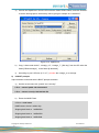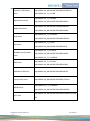
1
SBC8018 Evaluation Board Integrated with SATA, TF, OTG, Audio in/out, USB, Ethernet, LCD, CCD/COMS, Serial, JTAG interface based on 32-bit microprocessor User Manual Version update records: Rev Date Description 1.0 2011.10.21 Initial version Copyright © 2011 by element14 -2- User Manual Contents CHAPTER 1 OVERVIEW................................................................................................................. 6 1.1 PRODUCT INTRODUCTION .......................................................................................................... 6 1.2 FEATURES ................................................................................................................................ 7 CHAPTER 2 HARDWARE SYSTEM ............................................................................................... 9 2.1 CPU......................................................................................................................................... 9 2.1.1 CPU Introduction .............................................................................................................. 9 2.1.2 CPU Features .................................................................................................................. 9 2.2 INTRODUCTION TO THE EXPANDED CHIP: ..................................................................................11 2.2.1 TPS65070 .......................................................................................................................11 2.2.2 K9F1G08U0B ..................................................................................................................11 2.2.3 H5MS1G62MFP ............................................................................................................. 12 2.2.4 DM9161 .......................................................................................................................... 12 2.2.5 TLV320AIC33IRGZR...................................................................................................... 12 2.2.6 MAX3232 ....................................................................................................................... 12 2.3 HARDWARE INTERFACE ........................................................................................................... 13 2.3.1 Power Input Jack............................................................................................................ 13 2.3.2 Power Output Interface .................................................................................................. 14 2.3.3 Power Switch ................................................................................................................. 14 2.3.4 TFT_LCD Interface ........................................................................................................ 14 2.3.5 AUDIO OUTPUT Jack .................................................................................................... 16 2.3.6 Camera Interface ........................................................................................................... 17 2.3.7 MIC IN Jack.................................................................................................................... 18 2.3.8 Serial Ports ..................................................................................................................... 18 2.3.9 LAN Interface ................................................................................................................. 19 2.3.10 SATA Interface ............................................................................................................. 19 2.3.11 USB OTG Interface ...................................................................................................... 20 2.3.12 USB HOST Interface .................................................................................................... 21 2.3.13 TF Card Interface ......................................................................................................... 21 Copyright © 2011 by element14 -3- User Manual 2.3.14 JTAG Interface ............................................................................................................. 22 2.3.15 Expansion Interface ..................................................................................................... 22 2.3.16 DIP Switch .................................................................................................................... 25 2.3.17 KEY Switch .................................................................................................................. 26 2.3.18 LEDs............................................................................................................................. 26 CHAPTER 3 LINUX OPERATING SYSTEM ................................................................................. 27 3.1 INTRODUCTION........................................................................................................................ 27 3.2 SOFTWARE RESOURCES ......................................................................................................... 27 3.3 BOARD SUPPORT PACKAGE (BSP) FEATURES ......................................................................... 28 3.4 SYSTEM DEVELOPMENT .......................................................................................................... 29 3.4.1 How to Setup Operating System Development Environment ....................................... 29 3.4.2 System Compilation ....................................................................................................... 30 3.4.3 System Customization ................................................................................................... 33 3.5 HOW TO UPDATE THE SYSTEM IMAGE ...................................................................................... 37 3.5.1 Boot-up From Serial Port ............................................................................................... 37 3.5.2 How Update Images From Ethernet .............................................................................. 38 3.6 TEST PROCEDURES ................................................................................................................ 42 3.6.1 Various Tests Scenario................................................................................................... 42 3.7 APPLICATION DEVELOPMENT ................................................................................................... 51 CHAPTER 4 WINCE OPERATING SYSTEM ................................................................................ 53 4.1 INTRODUCTION........................................................................................................................ 53 4.2 SOFTWARE RESOURCES ......................................................................................................... 53 4.3 SOFTWARE FEATURES ............................................................................................................ 54 4.4 SYSTEM DEVELOPMENT .......................................................................................................... 56 4.4.1 Installation of IDE(Integrated Development Environment) ............................................ 56 4.4.2 Extract BSP and project files to IDE .............................................................................. 56 4.4.3 Sysgen & Build BSP ...................................................................................................... 57 4.4.4 Source code path of all drivers in BSP .......................................................................... 58 4.5 HOW TO UPDATE SYSTEM IMAGE ............................................................................................. 60 Copyright © 2011 by element14 -4- User Manual 4.5.1 Downloading EBOOT to NAND Flash ........................................................................... 60 4.5.2 Update TF Card NK runtime images ............................................................................. 63 4.5.3 Downloading NK.bin to NAND flash .............................................................................. 71 4.6 USER INSTRUCTIONS .............................................................................................................. 75 4.6.1 How to use Power Management.................................................................................... 75 4.6.2 How to use CAM8000-A module.................................................................................... 76 4.7 SBC8018 W INDOWS CE 6.0 WIN32 API APPLICATION DEVELOPMENT DEMO ............................ 77 APPENDIX ..................................................................................................................................... 78 APPENDIX I: HARDWARE DIMENSIONS............................................................................................ 78 APPENDIX II: THE INSTALLATION OF UBUNTU ................................................................................. 79 APPENDIX III: DRIVER INSTALLATION FOR LINUX USB ETHERNET/RNDIS GADGET ......................... 94 APPENDIX IV: THE SETUP OF TFTP SERVER ................................................................................. 97 CUSTOMER SERVICE & TECHNICAL SUPPORT ...................................................................... 99 CUSTOMER SERVICE..................................................................................................................... 99 TECHNICAL SUPPORT ................................................................................................................... 99 NOTES.......................................................................................................................................... 99 Copyright © 2011 by element14 -5- User Manual Chapter 1 Overview 1.1 Product Introduction The SBC8018 evaluation board is a compact, low-cost with high-performance evaluation board based on Texas instruments (TI) AM1808 microprocessor. AM1808 is an integration of 375 MHz ARM9 low-power application processor with 128K-Byte On-the chip memory, and provided lots of peripheral interface. SBC8018 board expands the hardware capabilities including LAN port, audio input/output interface, USB OTG, USB HOST, SATA interface, TF slot, serial port, JTAG interface, camera interface, TFT LCD interface, touch screen interface and keyboard interface. SBC8018 board can be used for the following applications: Intelligent instrument Service point Educational plant Portable data terminal Placeholder intelligent sensor A formal data terminal Industrial Control Home Automation Copyright © 2011 by element14 -6- User Manual Figure 1-1 SBC8018 Evaluation Board Functional Block Diagram 1.2 Features SBC8018 evaluation board is based on AM1808 processor and is one compact board which integrates all functions and features of TI’s AM1808 ARM9 processor. Some of the board features are mentioned below: Mechanical Parameters Working temperature: 0°C ~ 70°C Humidity Range: 20% ~ 90%, non-condensable Dimensions: 112.24mm x 82.29mm Power Consumption: [email protected] (working without LCD) Power Input: +5V/2A Processor 375-MHz ARM926EJ-S™ RISC Core ARM926EJ-S Core Memory 128MB NAND Flash Copyright © 2011 by element14 -7- User Manual 128MB Mobile DDR Audio/Video Interfaces An audio Microphone input interface (3.5mm audio jack, red) A two-channel audio line output interface (3.5mm audio jack, green) A TFT-LCD interface (24 bit color, 1.8 V logic, with touch screen) Data Transfer Interface Serial port: UART1, 3 line serial port, TTL based voltage UART2, 3 line serial port, TTL based voltage UART3, 5 line serial port, RS232 based voltage 1 x USB 2.0 OTG interface (OTG connector) 1 x USB1.1 Interface (Type A) 10/100Mbps Ethernet Interface (RJ45 jack) 1 channel TF card slot 1 channel SATA interface (supports both SATA I (1.5 Gbps) and SATA II (3.0 Gbps)) 1 channel 14-pin JTAG interface Multi-functional expand interface(IIC, SPI, MCBSP, UART, 1.8V, 3.3V, 5V, GPIO, EMA) Input Interface 2 x Camera interfaces (8 bit, 1.8 V logic) 4 buttons (RESET,BACK,HOME,MENU) 1 Power LED 3 User LEDs LED Copyright © 2011 by element14 -8- User Manual Chapter 2 Hardware System 2.1 CPU 2.1.1 CPU Introduction The AM1808 microprocessor contains an ARM RISC CPU for general-purpose processing and systems control. The AM1808 ARM microprocessor consists of the following primary components: ARM926EJ-S RISC processor core and associated memories A set of I/O peripherals A powerful DMA subsystem and SDRAM EMIF interface 2.1.2 CPU Features Clock The OSCIN/ OSCOUT system input clock (24 MHz) is used to generate the main source clock for the device. It also provides the DPLLs to several CPU other modules. Reset The function of reset is determined by the input signal on RESETN pin of the CPU, Reset is enabled when LOW level signal (high to low) is given. ARM Subsystem The ARM Subsystem includes the following features: ARM926EJ-S RISC processor ARMv5TEJ (32/16-bit) instruction set Little endian System Control Co-Processor 15 (CP15) MMU 16KB Instruction cache 16KB Data cache Write Buffer Embedded Trace Module and Embedded Trace Buffer (ETM/ETB) ARM Interrupt controller Copyright © 2011 by element14 -9- User Manual ARM926EJ-S RISC CPU The ARM Subsystem integrates the ARM926EJ-S processor. The ARM926EJ-S processor is a member of ARM9 family of general-purpose microprocessors. This processor is targeted at multi-tasking applications where full memory management, high performance, low die size, and low power are all important. The ARM926EJ-S processor supports the 32-bit ARM and 16 bit THUMB instruction sets, enabling the user to trade off between high performance and high code density. Specifically, the ARM926EJ-S processor supports the ARMv5TEJ instruction set, which includes features for efficient execution of Java byte codes, providing Java performance similar to Just in Time (JIT) Java interpreter, but without associated code overhead. The ARM926EJ-S processor supports the ARM debug architecture and includes logic to assist in both hardware and software debug. The ARM926EJ-S processor has a Harvard architecture and provides a complete high performance subsystem, including: ARM926EJ -S integer core CP15 system control coprocessor Memory Management Unit (MMU) Separate instruction and data caches Write buffer Separate instruction and data (internal RAM) interfaces Separate instruction and data AHB bus interfaces Embedded Trace Module and Embedded Trace Buffer (ETM/ETB) ARM Internal Memory 8 KB RAM 64 KB built-in ROM Embedded Trace Module and Embedded Trace Buffer (ETM/ETB) Copyright © 2011 by element14 - 10 - User Manual Figure 2-1 ARM Subsystem 2.2 Introduction to the Expanded Chip: 2.2.1 TPS65070 The TPS6507x are single chip Power Management IC, the charger can either be supplied by a USB port on pin USB or by a DC voltage from a wall adapter connected to pin. Three highly efficient 2.25MHz step-down converters are targeted at providing the core voltage, memory and I/O voltage in a processor based system. The step-down converters allow the use of small inductors and capacitors to achieve a small solution size. The TPS6507x also integrate two general purpose LDOs for an output current of 200mA. These LDOs can be used to power a TF-card interface and an always-on rail, but can be used for other purposes as well. Each LDO operates with an input voltage range between 1.8V and 6.3V allowing them to be supplied from one of the step-down converters or directly from the main battery. 2.2.2 K9F1G08U0B The K9F1G08U0B is the 128MB NAND flash memory chips used in SBC8018 evaluation board. This NAND Flash chip is directly interfaced to the CPU for faster memory access and read/write cycles. Copyright © 2011 by element14 - 11 - User Manual 2.2.3 H5MS1G62MFP The H5MS1G62MFP-K3M is the 128MB DDR memory chip used in SBC8018 evaluation board, This DDR RAM is connected directly the CPU DDR/SDRAM interface for faster memory access. 2.2.4 DM9161 The DM9161 is a fully integrated and cost-effective low pin count single chip Fast Ethernet controller with a general processor interface, a 10/100M PHY and 4K DWORD SRAM. It is designed with low power and high performance process that support 3.3V with 5V I/O tolerance. SBC8018 uses 10/100M adaptive network interface of DM9161, in which, the 10/100M Ethernet module is compatible to IEEE 802.3 standard protocol. The cable interface used is a standard RJ45 cable, with a connection indicator and a transmission indicator. 2.2.5 TLV320AIC33IRGZR The TLV320AIC33IRGZR is a low-power stereo audio codec with stereo headphone amplifier, as well as ten audio inputs and seven audio outputs programmable in single-ended or fully differential configurations. Extensive register enabling the stereo 48 kHz DAC playback as low as 15 mw from a 3.3V analog supply, making it ideal for portable battery-powered audio and telephony applications. The playback path includes mix/mux capability from the stereo DAC and selected inputs, through programmable volume controls, to the various outputs. TLV320AIC33IRGZR has Ten Audio Input Pins and Seven Audio Output Drivers. 2.2.6 MAX3232 The function of MAX3232 is mainly to convert TTL logic level signal to RS232 logic level, which helps the board at TTL logic to interface with PC working at RS232 logic level. The SBC8018 evaluation board uses UART2 as debugger serial port; the default voltage for this UART2 is 1.8V, Copyright © 2011 by element14 - 12 - User Manual it is necessary to convert this voltage from 1.8V to 3.3V in order to connect the board to the eternal world. . 2.3 Hardware Interface The following section provides you the detailed information on the peripherals, with the pin description, and its functionality available on SBC8018 evaluation board. Figure 2-2 Hardware Interface chart 2.3.1 Power Input Jack Table 2-1 power input interface J40 Pin Signal Function 1 GND GND 2 NC NC 3 +5V Power supply (+5V) 2A (Type) Copyright © 2011 by element14 - 13 - User Manual 2.3.2 Power Output Interface Table 2-2 power output interface J18 Pin Signal Function 1 +5V 5V output 2 GND GND 2.3.3 Power Switch Table 2-3 power switch SW1 Pin Signal Function 1 DC IN VDD Input 2 +5VDC_IN +5V 3 NC NC 2.3.4 TFT_LCD Interface Table 2-4 TFT_LCD interface J1 Pin Signal Function 1 B_NU0 Test Point 2 B_NU1 Test Point 3 B_NU2 Test Point 4 LCD_D0 LCD data bit0 5 LCD_D1 LCD data bit1 6 LCD_D2 LCD data bit2 7 LCD_D3 LCD data bit3 8 LCD_D4 LCD data bit4 9 GND GND Copyright © 2011 by element14 - 14 - User Manual 10 G_NU0 Test Point 11 G_NU1 Test Point 12 LCD_D5 LCD data bit5 13 LCD_D6 LCD data bit6 14 LCD_D7 LCD data bit7 15 LCD_D8 LCD data bit8 16 LCD_D9 LCD data bit9 17 LCD_D10 LCD data bit10 18 GND GND 19 R_NU0 Test Point 20 R_NU1 Test Point 21 R_NU2 Test Point 22 LCD_D11 LCD data bit11 23 LCD_D12 LCD data bit12 24 LCD_D13 LCD data bit13 25 LCD_D14 LCD data bit14 26 LCD_D15 LCD data bit15 27 GND GND 28 R_LCD_DEN LCD AC bias enable chip select 29 R_LCD_HSYNC LCD vertical sync 30 R_LCD_VSYNC LCD horizontal sync 31 GND GND 32 R_LCD_DCLK LCD Pixel Clock 33 GND GND 34 TOUCH_X1 Input 1 to the x-plate for the touch screen 35 TOUCH_X2 Input 2 to the x-plate for the touch screen 36 TOUCH_Y1 Input 1 to the y-plate for the touch screen 37 TOUCH_Y2 Input 2 to the y-plate for the touch screen 38 R_LCD_SPICLK SPI clock 39 R_LCD_MOSI Slave data in, master data out Copyright © 2011 by element14 - 15 - User Manual 40 R_LCD_MISO Slave data out, master data in 41 R_LCD_SPICS SPI enable 42 IIC_CLK IIC master serial clock, NC 43 IIC_DAT IIC serial bidirectional data, NC 44 GND GND 45 +1P8V_LDO +1.8V 46 +3P3V +3.3V 47 +5VDC_IN +5V 48 +5VDC_IN +5V 49 RESET +1.8V 50 R_LCD_PWREN Power on enable 2.3.5 AUDIO OUTPUT Jack Table 2-5 Audio out interface J38 Pin Signal Function 1 GND GND 2 LINE_OUT_LP Left output 3 LINE_OUT_RP Right output 4 LINE_OUT_RP Right output 5 LINE_OUT_LP Left output Copyright © 2011 by element14 - 16 - User Manual 2.3.6 Camera Interface Table 2-6 camera interface J35,J43 Pin Signal Function 1 GND GND 2 D0 Test Point 3 D1 Test Point 4 R_CAM_D0 VPIF capture data bit 0 5 R_CAM_D1 VPIF capture data bit 1 6 R_CAM_D2 VPIF capture data bit 2 7 R_CAM_D3 VPIF capture data bit 3 8 R_CAM_D4 VPIF capture data bit 4 9 R_CAM_D5 VPIF capture data bit 5 10 R_CAM_D6 VPIF capture data bit 6 11 R_CAM_D7 VPIF capture data bit 7 12 D10 Test Point 13 D11 Test Point 14 GND GND 15 PCLK Pixel clock 16 GND GND 17 CAM_HS_A0 Horizontal synchronization 18 +5VDC_IN 5V 19 CAM_VS_A0 Vertical synchronization 20 +3P3V 3.3V 21 CAM_XCLKA_A0 Test Point 22 CAM_XCLKB_A0 Test Point 23 GND GND 24 CAM_FLD_A0 Test Point 25 uP_CAM_WEN0 Test Point 26 uP_CAM_STR Test Point Copyright © 2011 by element14 - 17 - User Manual 27 CAM_SDA I2C0 serial data 28 CAM_SCL I2C0 serial clock 29 GND GND 30 +1P8V_LDO 1.8V 2.3.7 MIC IN Jack Table 2-7 MIC IN interface J39 Pin Signal Function 1 GND GND 2 LINE_IN_LP Left input 3 LINE_IN_RP Right input 4 LINE_IN_RP Right input 5 LINE_IN_LP Left input 2.3.8 Serial Ports Table 2-8 serial port J9 Pin Signal Function 1 NC NC 2 RSA_RXD Receive data 3 RSA_TXD Transit data 4 NC NC 5 GND GND 6 NC NC 7 RSA_RTS Request To Send 8 RSA_CTS Clear To Send 9 NC NC 10 GND GND 11 GND GND Copyright © 2011 by element14 - 18 - User Manual 2.3.9 LAN Interface Table 2-9 LAN interface J58 Pin Signal Function 1 LAN_TX+ TX+ output 2 LAN_TX- TX- output 3 CT Link to analog transmit power input with 0R resistance 4 4&5 Transformer 5 7&8 Transformer 6 CT Link to analog transmit power input with 0R resistance 7 LAN_RX+ RX+ input 8 LAN_RX- RX- input 9 YEL Link LED 10 VDD 3.3V Power for LED 11 GRN Speed LED 12 VDD 3.3V Power for LED 13 CHGND GND 14 CHGND GND 15 NC NC 16 NC NC 2.3.10 SATA Interface Table 2-10 SATA interface J32 Pin Signal Function 1 GND GND 2 SATA_TXP SATA receive data(positive) Copyright © 2011 by element14 - 19 - User Manual 3 SATA_TXN SATA receive data(negative) 4 GND GND 5 SATA_RXN SATA transmit data(negative) 6 SATA_RXP SATA transmit data(positive) 7 GND GND 8 NC NC 9 GND GND 2.3.11 USB OTG Interface Table 2-11 USB OTG interface J34 Pin Signal Function 1 USB0_VBUS +5V 2 USB0_D- USB Data- 3 USB0_D+ USB Data+ 4 ID USB ID 5 GND GND 6 G2 GND 7 G3 GND 8 G4 GND 9 G5 GND 10 G6 GND 11 NC NC 12 NC NC Copyright © 2011 by element14 - 20 - User Manual 2.3.12 USB HOST Interface Table 2-12 USB HOST interface J33 Pin Signal Function 1 USB1_VBUS +5V 2 USB1_D- USB Data- 3 USB1_D+ USB Data+ 4 GND GND 5 CHGND GND 6 CHGND GND 2.3.13 TF Card Interface Table 2-13 TF interface J36 Pin Signal Function 1 DAT2 Card data 2 2 DAT3 Card data 3 3 CMD Command Signal 4 VDD VDD 5 CLK Clock 6 VSS GND 7 DAT0 Card data 0 8 DAT1 Card data 1 9 CD Card detect 10 PGND GND 11 PGND GND 12 PGND GND 13 PGND GND 14 NC NC 15 NC NC Copyright © 2011 by element14 - 21 - User Manual 2.3.14 JTAG Interface Table 2-14 JTAG interface J37 Pin Signal Function 1 TMS Test mode select 2 NTRST Test system reset 3 TDI Test data input 4 GND GND 5 VIO 1.8V 6 NC NC 7 TDO Test data output 8 GND GND 9 RTCK Receive test clock 10 GND GND 11 TCK Test clock 12 GND GND 13 EMU0 Test emulation 0 14 EMU1 Test emulation 1 2.3.15 Expansion Interface Table 2-15 expansion interface J41 Pin Signal Function 1 GND GND 2 GND GND 3 EMA_A_16_EXP GPIO 4 EMA_D_15_EXP GPIO 5 EMA_A_15_EXP GPIO Copyright © 2011 by element14 - 22 - User Manual 6 EMA_D_14_EXP GPIO 7 EMA_A_14_EXP GPIO 8 EMA_D_13_EXP GPIO 9 EMA_A_13_EXP GPIO 10 EMA_D_12_EXP GPIO 11 EMA_A_0_EXP GPIO 12 EMA_D_11_EXP GPIO 13 EMA_BA_1_EXP GPIO 14 EMA_D_10_EXP GPIO 15 EPWMN1_TZ0 GPIO 16 EMA_D_9_EXP GPIO 17 ECAP2_APWM2 GPIO 18 EMA_D_8_EXP GPIO 19 AIC_WCLK GPIO 20 EMA_CLK_EXP GPIO 21 AFSR GPIO 22 EMA_SDCKE_EXP GPIO 23 AIC_MCLK GPIO 24 EMA_CSn_5_EXP GPIO 25 GND GND 26 EMA_CSn_4_EXP GPIO 27 AIC_BCLK GPIO 28 EMA_CSn_2_EXP GPIO 29 ACLKR GPIO 30 EMA_CSn_0_EXP GPIO 31 GND GND 32 EMA_WAIT_1_EXP GPIO 33 GND GND 34 GND GND 35 +5VDC_IN +5V 36 GND GND Copyright © 2011 by element14 - 23 - User Manual 37 +3P3V 3.3V 38 +1P8V_LDO 1.8V 39 GND GND 40 GND GND Table 2-16 expansion interface J42 Pin Signal Function 1 GND GND 2 GND GND 3 uP_SPI1_CLK SPI1 clock 4 uP_McBSP1_CLKR_EXP McBSP1 receive clock 5 uP_SPI1_SOMI SPI1 data slave-out-master-in 6 uP_McBSP1_CLKX_EXP McBSP1 transmit clock 7 uP_SPI1_SIMO SPI1 data slave-in-master-out 8 uP_McBSP0_CLKS_EXP 9 uP_SPI1_SCSn0 SPI1 chip selects 10 AIC_DOUT McBSP1 receive frame sync 11 uP_SPI1_ENAN SPI1 enable 12 AIC_DIN McBSP1 transmit frame sync 13 GND GND 14 uP_McBSP0_DR_EXP McBSP1 receive data 15 UART1_RXD UART1 receive data 16 uP_McBSP0_DX_EXP McBSP1 transmit data 17 UART1_TXD UART1 transmit data 18 GND GND 19 UART1_RTSn UART1 ready-to-send output 20 UART2_RXD UART2 receive data 21 AIC_MCL UART1 clear-to-send input 22 UART2_TXD UART2 transmit data 23 GND GND Copyright © 2011 by element14 - 24 - McBSP1 sample rate generator clock input User Manual 24 I2C0_SCL I2C0 serial clock 25 GND GND 26 I2C0_SDA I2C0 serial data 27 GND GND 28 GND GND 29 GND GND 30 uP_SPI0_CLK SPI0 clock 31 GDN GND 32 uP_SPI0_SOMI SPI0 data slave-out-master-in 33 GND GND 34 uP_SPI0_SIMO SPI0 data slave-in-master-out 35 GND GND 36 uP_SPI0_SCSn0 SPI0 chip selects 37 +5VDC_IN +5V 38 uP_SPI0_ENAN 1.8V 39 +3P3V +3.3V 40 +1P8V_LDO +1.8V 2.3.16 DIP Switch Table 2-17 DIP Switch S7 Pin Function 1 PWR_BOOT Link to PWR_BOOT with 1K resistor 2 GND Link to GND with 1K resistor 3 GND Link to GND with 1K resistor 4 PWR_BOOT Link to PWR_BOOT with 1K resistor 5 LCD_D12 LCD data bit 12 6 LCD_D11 LCD data bit 11 7 LCD_D10 LCD data bit 10 8 LCD_D9 LCD data bit 9 Copyright © 2011 by element14 - 25 - User Manual 2.3.17 KEY Switch Table 2-18 KEY Switch Key Pin Function S6 uP_RESETn Device reset input S8 USER_BACK GPIO S9 USER_MENU GPIO S10 USER_HOME GPIO 2.3.18 LEDs Table 2-19 LED LED Pin Signal Function D2 User_LED_1 User Definitude D3 User_LED_2 User Definitude D4 User_LED_3 User Definitude D5 +3P3V 3.3V power indicator Copyright © 2011 by element14 - 26 - User Manual Chapter 3 Linux Operating System 3.1 Introduction This section is intended to provide detailed instruction on Operating System Software development for SBC8018 evaluation board: 1) Describes the software resources provided by SBC8018. 2) Describes the software feature. 3) Explains the software development including how to set up the development environment, the building guidance of the boot loader, kernel and file system, and the development of device driver. 4) Provides flashing methods with U-BOOT prompts. 5) Shows the usage of SBC8018 6) Shows the application development. In this part, it is suggested to: 1) Install Ubuntu Linux in advance, please refer to Appendix II for details; 2) Master relative embedded Linux development technology. 3.2 Software Resources This chapter provides an overview of software system components of SBC8018. A basic software system consists of four parts: u-boot, kernel and rootfs. The Figure 3-2 shows the structure of the system: Figure 3-1 Copyright © 2011 by element14 - 27 - User Manual Features and functions of each part of the system are given below: 1) U-boot is a bootstrap program, it’s used for interacting with users and updating images and loading the kernel; 2) The latest 2.6.x kernel is employed here and it can be customized to use on SBC8018 evaluation board. 3) Rootfs employs Open-source system “jffs2”. 3.3 Board Support Package (BSP) Features The SBC8018 Board Support Package (BSP) is used for customizing and generating the Linux operating system applicable to SBC8018 hardware platform. Users can conduct a secondary development on the basis of this BSP. The BSP in the CD provided with the SBC8018 evaluation kit contains as bellows: Table 3-1 BSP Features Item Note NAND MMC/SD BIOS u-boot FAT NET Supports Kernel ROM/CRAM/EXT2/EXT3/FAT/NFS/ Linux-2.6.x JFFS2 and various file systems serial Series driver rtc Hardware clock driver net 10/100M Ethernet card DM9000 driver flash nand flash driver (supports nand boot) lcd TFT LCD driver touch screen Touch screen controller ads7846 driver tf mmc/sd controller driver Device Driver Debug usb otg 2.0 driver (can be configured as slave usb otg device currently) usb ehci Copyright © 2011 by element14 - 28 - usb ehci driver User Manual audio Audio driver Camera driver (support CAM8000-A camera camera module) button gpio button driver led user led lamp driver sata 1.5-3.0G SATA driver 3.4 System Development 3.4.1 How to Setup Operating System Development Environment Before executing software development on SBC8018, the user has to install Linux cross development environment on its computer. How to install a cross development environment will be explained below by taking Ubuntu operating system as an example. 3.4.1.1 Installation of Cross Compilation Tools Installation of cross compilation tools is done by using the software CD provided along with this kit, to start the process insert the CD and allow it for auto run, Ubuntu will mount the disc under the directory /media/cdrom, the cross compilation tools are saved under the directory /media/cdrom/linux/tools. mkdir $HOME/tools cd /media/cdrom/linux/tools tar -jxvf arm-2009q1-203-arm-none-linux-gnueabi-i686-pc-linux-gnu.tar.bz2 -C $HOME/tools 3.4.1.2 Installation of Other Tools Some of the other development tools used for source code compilation are present in the directory linux/tools; the user can execute the following commands to copy them to the local folder: cd /media/cdrom/linux/tools cp mkimage $HOME/tools cp mkfs.jffs2 $HOME/tools Copyright © 2011 by element14 - 29 - User Manual 3.4.1.3 Addition of environment variables After all above tools are installed, it is necessary to use the following commands to add them in the temporary environment variables: export PATH=$HOME/tools/arm-2009q1/bin:$HOME/tools:$PATH The user can write it in the .barsrc file under the user directory, such that the addition of environment variables will be finished automatically when the system is booted; command echo $PATH can be used to check the path. 3.4.2 System Compilation 3.4.2.1 Preparation Source codes for all the components of the system are available in the disc under the directory linux/source; users need to extract them to the Ubuntu system before starting the development: mkdir $HOME/work cd $HOME/work tar xvf /media/cdrom/linux/source/uboot-03.20.00.14.tar.bz2 tar xvf /media/cdrom/linux/source/linux-03.20.00.14.tar.bz2 cp /media/cdrom/linux/source/ramdisk ./ mkdir rootfs sudo mount –t ext2 –o loop ramdisk rootfs After completing the above steps, the current directory will generate uboot-03.20.00.14, linux-03.20.00.14 and rootfs directories. 3.4.2.2 X-loader Image Generation The SBC8018 evaluation board supports UART boot or NAND boot. The image files are different for the different boot modes, and the methods for mapping are also different. Copyright © 2011 by element14 - 30 - User Manual 1) To generate image file u-boot cd uboot-03.20.00.14 make distclean make da850evm_config make After completing the above steps, the current directory will generate the required u-boot file. Copy current u-boot file to Windows system, the AISgen tool will launch on Windows. 2) To generate the u-boot-uart-ais.bin for UART start-up Put the new u-boot file to the folder [d:\sbc8018]. Make sure you had installed “AISgen_d800k006_Install_v1.7.exe” under the folder [CD\linux\tools\]. Click Windows XP -> Start -> All Programs -> Texas Instruments -> AISgen for D800K006 -> AISgen for D800K006 to open AISgen tool. a) Launches the ASIgen, click “File”-> “Load Configuration” to open AM1808-UART.cfg from the CD under the folder CD\linux\tools\. b) Added the u-boot file under the folder [d:\sbc8018\] to the [ARM Application File:] c) Sets the output file path [AIS Output File] as [d:\sbc8018\u-boot-uart-ais.bin]. d) Click [Generate AIS], “u-boot-uart-ais.bin” will be generated under the folder [d:\sbc8018]. Copyright © 2011 by element14 - 31 - User Manual Figure 3-2 ASIgen for D800K006 3) To generate u-boot-nand-ais.bin for NAND Flash boot up a) Launches the ASIgen, click “File”-> “Load Configuration” to open AM1808-NAND.cfg under the folder CD\linux\tools\. b) Added the u-boot file under the folder [d:\sbc8018\] to the [ARM Application File:] c) Sets the output file path [AIS Output File] as [d:\sbc8018\u-boot-nand-ais.bin]. d) Click [Generate AIS], “u-boot-nand-ais.bin” will be generated under the folder [d:\sbc8018]. 3.4.2.3 Kernel compilation 1) Choose the Display Device Modify the lines as below according to the display screen size in the file: [linux-03.20.00.14/arch/arm/mach-davinci/board-da850-evm.c] For 4.3-inch LCD: #define LCD_4_3INCH 1 #define LCD_7INCH 0 For 7-inch LCD: #define LCD_4_3INCH Copyright © 2011 by element14 - 32 - 0 User Manual #define LCD_7INCH 1 2) Kernel compilation cd linux-03.20.00.14 make distclean make sbc8018_defconfig make uImage After completing the above steps, the required uImage file will be generated under the directory arch/arm/boot. 3.4.2.4 Generation of File System cd $HOME/work sudo $HOME/tools/mkfs.jffs2 –r rootfs –o jffs2.img After completing the above steps, the current directory will generate the the required “jffs2.img” file. 3.4.3 System Customization As Linux kernel has many configuration options, the user can increase or reduce the kernel features by using available default kernel configurations according to their best requirements. The general process of system customization is described with examples below; 3.4.3.1 Modification of Kernel Configuration The source code for factory default kernel configuration is provided in the below directory: [linux-03.20.00.14/arch/arm/configs/sbc8018_defconfig] User can carry out system customization on this basis: cd linux-03.20.00.14 cp arch/arm/configs/sbc8018_defconfig .config make menuconfig Copyright © 2011 by element14 - 33 - User Manual If an error occurs in the system when make menuconfig is input, it is necessary to install ncurse in the Ubuntu system; ncurse library is a character graphic library, used for make menuconfig of kernel; the specific installation instruction is: sudo apt-get install ncurses-dev How do perform the system customization is described below using USB gadget and USB mass storage device as an example: 1) Select Device driver Figure 3-3 2) Select USB support Copyright © 2011 by element14 - 34 - User Manual Figure 3-4 3) Select USB Gadget Support Figure 3-5 Copyright © 2011 by element14 - 35 - User Manual 4) The configuration of USB Gadget Support can be changed as showed in the following: Figure 3-6 3.4.3.2 Compilation Save the configuration made and execute the following commands to recompile the kernel: make uImage make modules After completing the above steps, a new kernel image uImage and a module file g_file_storage.ko will be generated under the directory “arch/arm/boot” and “drivers/usb/gadget” respectively. 3.4.3.3 Test To perform the test first you need to update the kernel image ulmage file, after that copy the g_file_storage.ko file to the TF card and reboot the system. Now execute the following commands to stimulate the TF card into USB mass storage device to use with PC: root@sbc8018:~# cd /media/mmcblk0p1/ root@sbc8018:/media/mmcblk0p1# insmod g_file_storage.ko file=/dev/mmcblk0p1 stal l=0 removable=1 g_file_storage gadget: File-backed Storage Gadget, version: 20 November 2008 g_file_storage gadget: Number of LUNs=1 g_file_storage gadget-lun0: ro=0, file: /dev/mmcblk0p1 musb_hdrc musb_hdrc: MUSB HDRC host driver Copyright © 2011 by element14 - 36 - User Manual musb_hdrc musb_hdrc: new USB bus registered, assigned bus number 3 hub 3-0:1.0: USB hub found hub 3-0:1.0: 1 port detected musb g_file_storage gadget disconnected. root@sbc8018:/media/mmcblk0p1# g_file_storage gadget: high speed config #1 Use the USB cable (USB mini B to USB A) to connect the development board and PC, PC will prompt a message to indicate USB mass storage device is found; a new portable hard disk is found and now users is ready to use the disk. Please make sure that the kernel image has been updated, otherwise, module g_file_storage.ko will fail to load and the similar tips will show: insmod: cannot insert '/media/mmcblk0p1/g_file_storage.ko': Device or resource busy 3.5 How to Update the System Image The SBC8018 evaluation board NAND Flash by default comes with the installed Linux + 4.3-inch screen display. It can be booted without connecting TF card once it’s powered ON or RESET and input “root” to enter Linux system. Please make sure the DIP switch [S7] settings are as below: Figure 3-7 Boot-up from NAND Flash 3.5.1 Boot-up From Serial Port 1) First setup the hardware environment, make sure the DIP switch [S7] settings are as below: Figure 3-8 Boot-up from Serial port 2) Now open the AISgen_d800k006_Install_v1.7.exe: Copyright © 2011 by element14 - 37 - User Manual Windows XP -> Start -> All Programs -> Texas Instruments -> AISgen for D800K006 -> UART Boot Host Add u-boot-uart-ais.bin [Directory: CD\linux\image\] to the “AIS-File” as below: Figure 3-9 3) Click the “Start” and power ON the evaluation board to boot-up from serial port. 4) Wait for moment, the target window will display “(Serial Port): Closing COM1.”, close the tool and open the Hyperterminal to catch the serial port information. User should open Hyperterminal and Input any key to enter U-BOOT prompts in three seconds, or else U-BOOT will load default parameter. 3.5.2 How Update Images From Ethernet The SBC8018 evaluation board image can be updated through Ethernet port as well, in thi section we will explain how to update the image using Ethernet port. Below IP will be taken as an example; PC: 192.192.192.154 Evaluation board: 192.192.192.215 1) PC TFTP service Copyright © 2011 by element14 - 38 - User Manual a) Launch the “tftpd32.exe” from the CD under the folder CD\linux\tools, and click “Browse” to set the sharing space, the directory will be giving an example as “d:\sbc8018”. Figure 3-10 tftpd32 tool b) Copy “u-boot-nand-ais.bin”, “uImage_4.3”, “uImage_7”, “jffs2.img” from the CD under the folder [CD\linux\image\] to the folder [d:\sbc8018] c) 2) According to your LCD size (4.3" or 7"), rename the uImage_xx as uImage. U-BOOT prompts Input the below commands with U-BOOT prompts as below: a) Set the environment with “ipaddr” and “serverip”: U-Boot > setenv ipaddr 192.192.192.215 U-Boot > setenv serverip 192.192.192.154 b) Erase the NAND Flash U-Boot > nand erase NAND erase: device 0 whole chip Skipping bad block at 0x0ff80000 Skipping bad block at 0x0ffa0000 Skipping bad block at 0x0ffc0000 Copyright © 2011 by element14 - 39 - User Manual Skipping bad block at 0x0ffe0000 OK c) Write U-BOOT U-Boot > tftp 0xc0700000 u-boot-nand-ais.bin;nand write.i 0xc0700000 0x20000 ${filesize} Using device TFTP from server 192.192.192.154; our IP address is 192.192.192.215 Filename 'u-boot-nand-ais.bin'. Load address: 0xc0700000 Loading: ############### done Bytes transferred = 210860 (337ac hex) NAND write: device 0 offset 0x20000, size 0x337ac 210944 bytes written: OK U-Boot > nandecc sw SW ECC selected d) Write kernel U-Boot > tftp 0xc0700000 uImage;nand write.i 0xc0700000 0x200000 ${filesize} Using device TFTP from server 192.192.192.154; our IP address is 192.192.192.215 Filename 'uImage'. Load address: 0xc0700000 Loading: ################################################################# ################################################################# ########################### done Bytes transferred = 2299460 (231644 hex) NAND write: device 0 offset 0x200000, size 0x231644 Copyright © 2011 by element14 - 40 - User Manual 2299904 bytes written: OK e) Write file system U-Boot > tftp 0xc2000000 jffs2.img;nand write.i 0xc2000000 0x600000 ${filesize} Using device TFTP from server 192.192.192.154; our IP address is 192.192.192.215 Filename 'jffs2.img'. Load address: 0xc2000000 Loading: ################################################################# ######T ########################################################### ################################################################# #######################################################T ######### ##### done Bytes transferred = 3889116 (3b57dc hex) NAND write: device 0 offset 0x600000, size 0x3b57dc 3889152 bytes written: OK 3) NAND Flash boot-up For NAND flash boot up make sure the DIP switch [S7] settings are as below: Figure 3-11 Boot-up from NAND Flash Copyright © 2011 by element14 - 41 - User Manual #T 3.6 Test Procedures 3.6.1 Various Tests Scenario 3.6.1.1 LED Testing The SBC8018 evaluation board is having following LEDs: D5 is power LED D2 is heartbeat LED D3 and D4 are user’s LED The following operation can be carried out using HyperTerminal: 1) Control D3 root@sbc8018:~# echo 0 > /sys/class/leds/led2/brightness root@sbc8018:~# echo 1 > /sys/class/leds/led2/brightness 2) Control D4 root@sbc8018:~# echo 0 > /sys/class/leds/led3/brightness root@sbc8018:~# echo 1 > /sys/class/leds/led3/brightness 3.6.1.2 Key Switch Testing The SBC8018 evaluation board is having three users key switches S8, S9 and S10; users can perform the following testing: First, enter the following command, and then press the S9, S8, S10 keys root@sbc8018:~# hexdump /dev/input/event0 0000000 06f5 49e5 206f 0001 0001 0100 0000 0000 0000010 06f5 49e5 208d 0001 0000 0000 0000 0000 0000020 06f5 49e5 1c89 0003 0001 0100 0001 0000 0000030 06f5 49e5 1ca9 0003 0000 0000 0000 0000 0000040 07b5 49e5 d3fd 0008 0001 0101 0000 0000 0000050 07b5 49e5 d41d 0008 0000 0000 0000 0000 0000060 07b5 49e5 63d9 000b 0001 0101 0001 0000 0000070 07b5 49e5 63fc 000b 0000 0000 0000 0000 Copyright © 2011 by element14 - 42 - User Manual 0000080 07b6 49e5 2569 000c 0001 0102 0000 0000 0000090 07b6 49e5 2586 000c 0000 0000 0000 0000 00000a0 07b6 49e5 a922 000e 0001 0102 0001 0000 00000b0 07b6 49e5 a941 000e 0000 0000 0000 0000 Press CONTROL+C to quit the test. The back of the test is the same. 3.6.1.3 Touch Screen Testing 1) Run the following command to start the calibration process: root@sbc8018:~# ts_calibrate Then follow the LCD prompt, click the "+" icon 5 times to complete the calibration 2) Calibration is complete, now enter the following commands for Touch Panel Test: root@sbc8018:~# ts_test Follow the LCD prompts to choose draw point OR draw line test. 3.6.1.4 RTC Testing The development board contains the hardware clock for save and to synchronize the system time. User can perform the RTC test by following steps below: 1) Set the system time as Mon Dec 05 20:00:00 2011 root@sbc8018: # date 120520002011 Mon Dec 08 20:00:00 UTC 2011 2) Write the system clock into RTC root@sbc8018:~# hwclock -w 3) Read the RTC root@sbc8018: # hwclock Mon Dec 08 20:00:00 UTC 2011 Now the RTC clock has been set as Dec 05 2011; the system clock will be saved in the hardware clock. Copyright © 2011 by element14 - 43 - User Manual 4) Restart the system, enter the following commands to renew the system clock root@sbc8018: # hwclock -s root@sbc8018: # date Mon Dec 08 20:00:00 UTC 2011 Now the system time has been set as hardware time. The SBC8018 Development board RTC battery can use model CR1220, user needs to prepare themselves. 3.6.1.5 TF Card Testing 1) First insert the TF card in the board, the system will automatically mount the file system of the TF card under the directory /media: root@sbc8018:~# cd /media/ root@sbc8018:/media# ls 2) card hdd cf mmc1 mmcblk0p1 ram net union realroot Enter the following command to see the TF card content: root@SBC80root@sbc801818:/media# ls mmcblk0p1/ flash-uboot.bin u-boot.bin mlo uImage ramdisk.gz ubi.img x-load.bin.ift_for_NAND 3.6.1.6 USB Devices Testing In the USB DEVICE testing, a USB cable is used to connect the miniUSB interface of the development board and the USB interface of the PC; for the computer end, the development board is recognized as a network device. 1) The computer needs to be installed with Linux USB Ethernet driver, please refer to Appendix III for detailed installation procedure. Copyright © 2011 by element14 - 44 - User Manual 2) After booting the system, please configure the system using the below commands through HyperTerminal: root@Sbc8018:~# ifconfig usb0 192.168.1.115 root@Sbc8018:~# ifconfig lo Link encap:Local Loopback inet addr:127.0.0.1 Mask:255.0.0.0 UP LOOPBACK RUNNING MTU:16436 Metric:1 RX packets:26 errors:0 dropped:0 overruns:0 frame:0 TX packets:26 errors:0 dropped:0 overruns:0 carrier:0 collisions:0 txqueuelen:0 RX bytes:2316 (2.2 KiB) TX bytes:2316 (2.2 KiB) usb0 Link encap:Ethernet HWaddr 5E:C5:F6:D4:2B:91 inet addr:192.168.1.115 Bcast:192.168.1.255 Mask:255.255.255.0 UP BROADCAST RUNNING MULTICAST MTU:1500 Metric:1 RX packets:253 errors:0 dropped:0 overruns:0 frame:0 TX packets:43 errors:0 dropped:0 overruns:0 carrier:0 collisions:0 txqueuelen:1000 RX bytes:35277 (34.4 KiB) TX bytes:10152 (9.9 KiB) 3) After the development board is configured, please click My Computer>>Network Neighborhood>>Check Network Connection; you can see a virtual network adapter is added at the PC end. 4) Now go to the virtual network adapter properties and select “Internet Protocol (TCP/IP)” to configure the IP address of the virtual network adapter: Copyright © 2011 by element14 - 45 - User Manual Figure 3-12 5) Now use the ping command from the HyperTerminal to test whether the development board IP address has been configured successfully. root@Sbc8018:~# ping 192.168.1.15 PING 192.168.1.15 (192.168.1.15): 56 data bytes 64 bytes from 192.168.1.15: seq=0 ttl=128 time=0.885 ms 64 bytes from 192.168.1.15: seq=1 ttl=128 time=0.550 ms 6) If you receive ping response like above, indicates the successful communication between the board and the PC. IP address of the network adapter configured in OTG cannot be the same as that of Ethernet interface. Copyright © 2011 by element14 - 46 - User Manual 3.6.1.7 USB HOST Testing 1) Connect the USB flash disk, the system will automatically mount the file system of the USB flash disk under the directory /media: root@sbc8018:~# cd /media/ root@sbc8018:/media# ls 2) card hdd mmcblk0p1 ram cf mmc1 net realroot sda1 union You can see the USB flash disk contents using the below command: root@sbc8018:/media# ls sda1/ flash-uboot.bin u-boot.bin mlo uImage ramdisk.gz ubi.img x-load.bin.ift_for_NAND 3.6.1.8 Audio Testing The board has multiple audio input and output interface, we can use the “alsa-utils” utility available in the file system to test the board audio, in order to test the audio please follow the below steps; 1) Recording Test: To test the recording functionality, first plug-in the microphone and use the below command to start the recording: root@Sbc8018:~# arecord -t wav -c 1 -r 44100 -f S16_LE -v k Recording WAVE 'k' : Signed 16 bit Little Endian, Rate 44100 Hz, Stereo Plug PCM: Hardware PCM card 0 'omap3evm' device 0 subdevice 0 Its setup is: stream : CAPTURE access : RW_INTERLEAVED format : S16_LE subformat : STD channels :2 rate : 44100 Copyright © 2011 by element14 - 47 - User Manual exact rate msbits : 44100 (44100/1) : 16 buffer_size : 22052 period_size : 5513 period_time : 125011 tstamp_mode : NONE period_step : 1 avail_min : 5513 period_event : 0 start_threshold : 1 stop_threshold : 22052 silence_threshold: 0 silence_size : 0 boundary appl_ptr hw_ptr 2) : 1445199872 :0 :0 Playback Testing: To playback, plug-in the headphones and enter the below command to hear what you have just recorded; root@Sbc8018:~# aplay -t wav -c 2 -r 44100 -f S16_LE -v k Playing WAVE 'k' : Signed 16 bit Little Endian, Rate 44100 Hz, Stereo Plug PCM: Hardware PCM card 0 'omap3evm' device 0 subdevice 0 Its setup is: stream : PLAYBACK access : RW_INTERLEAVED format : S16_LE subformat : STD channels :2 rate : 44100 Copyright © 2011 by element14 - 48 - User Manual exact rate msbits : 44100 (44100/1) : 16 buffer_size : 22052 period_size : 5513 period_time : 125011 tstamp_mode : NONE period_step : 1 avail_min : 5513 period_event : 0 start_threshold : 22052 stop_threshold : 22052 silence_threshold: 0 silence_size : 0 boundary appl_ptr hw_ptr : 1445199872 :0 :0 3.6.1.9 Network Testing 1) The board is having a 10/100M self-adapting DM9000 network card, users can directly connect the board to the LAN network and enter the following commands for network testing: root@sbc8018:~# ifconfig eth0 192.192.192.203 root@sbc8018:~# # ifconfig eth0 Link encap:Ethernet HWaddr 00:11:22:33:44:55 inet addr:192.192.192.203 Bcast:192.192.192.255 Mask:255.255.255.0 UP BROADCAST MULTICAST MTU:1500 Metric:1 RX packets:0 errors:0 dropped:0 overruns:0 frame:0 TX packets:0 errors:0 dropped:0 overruns:0 carrier:0 collisions:0 txqueuelen:1000 RX bytes:0 (0.0 B) TX bytes:0 (0.0 B) Interrupt:185 Base address:0x2000 Copyright © 2011 by element14 - 49 - User Manual root@sbc8018:~# ping 192.192.192.154 PING 192.192.192.154 (192.192.192.154): 56 data bytes 64 bytes from 192.192.192.154: seq=0 ttl=128 time=4.486 ms 64 bytes from 192.192.192.154: seq=1 ttl=128 time=0.336 ms 64 bytes from 192.192.192.154: seq=2 ttl=128 time=0.336 ms 2) If you receive ping response like above, indicates the successful network communication. The IP address in the network card of development board and PC should be in the same network segment, for example: 192.192.192.x. Press CONTROL+C to quit the test. 3.6.1.10 Camera Testing If you have bought the specific camera module for SBC8018 evaluation board, first connect the CAMERA module and LCD screen to the board. To install the camera please use the camera drivers from [drivers/media/video/tvp514x.c]. After installation of camera module enter the following command: root@Sbc8018:~# camera_test -i 0 -n 3 -f nv16 -S -s 720x576 /dev/video0 The framebuffer device was opened successfully. fscreen line_length : 960 vscreen 480x272, 16bpp, xoffset=0, yoffset=0 The framebuffer device mapped successfully. Device /dev/video0 opened: DA850/OMAP-L138 Video Capture. Once the above commands are executed you should be able to see the captured images from the camera module on your LCD screen. 3.6.1.11 SATA Testing 1) Connect SATA device to the SATA connector marked with J32, and connect the SATA device power cable to the J37 connector on the evaluation board. 2) Now power ON the evaluation board, you can see the SATA device contents by using the Copyright © 2011 by element14 - 50 - User Manual following command: root@sbc8018:~# ls -l /media/ drwxr-xr-x 2 root root 1024 Apr 15 2009 mmc1 drwxr-xr-x 2 root root 4096 Jan 1 1970 mmcblk0p1 drwxr-xr-x 2 root root 4096 Jan 1 1970 sda5 root@sbc8018:~# ls -l /media/sda5/ -rwxr-xr-x 1 root root 6 Apr 14 20:25 hello.txt -rwxr-xr-x 1 root root 30781440 Jul 28 2011 taobeini.WAV root@sbc8018:~# 3.7 Application Development This section will introduce you to the various steps involved in application development process: Step 1: Code Editing Source Code: led_app.c Application: Blinking D3 and D4 LEDS #include <stdio.h> #include <unistd.h> #include <fcntl.h> #define LED_D3 "/sys/class/leds/led2/brightness" #define LED_D4 "/sys/class/leds/led3/brightness" int main(int argc, char *argv[]) { int i; int f_led1, f_led2; unsigned char dat1, dat2; if((f_led1 = open(LED_D3, O_RDWR)) < 0){ printf("error in open %s", LED_D3); Copyright © 2011 by element14 - 51 - User Manual return -1; } if((f_led2 = open(LED_D4, O_RDWR)) < 0){ printf("error in open %s",LED_D4); return -1; } for(i = 0; i < 100; i++) { dat1 = (i & 0x1)? '1': '0'; dat2 = (i & 0x2)? '1': '0'; write(f_led1, &dat1, sizeof(dat1)); write(f_led2, &dat2, sizeof(dat2)); usleep(300000); } return 0; } Step 2: Cross-compilation arm-none-linux-gnueabi-gcc led_app.c -o led_app Step 3: Download and run Now download the compiled code into the evaluation board through TF card, USB flash disk or network, locate the the directory with the led_app file and enter the following commands and press Enter, to run led_app in the background. chmod a+x ./led_app ./led_app Copyright © 2011 by element14 - 52 - User Manual Chapter 4 WinCE Operating System 4.1 Introduction This section will introduces you to the SBC8018 evaluation board application development using Windows Embedded CE 6.0 R3, software resources on the disc, software features, installation of development environment, and how to “sysgen” and build BSP (board support package). 4.2 Software Resources BSP (Board Support Package) CD\WINCE600\BSP\OMAPL138_AM18X.rar CD\WINCE600\BSP\OMAPL13X_TI_V1.rar Windows Embedded CE 6.0 R3 sample project CD\WINCE600\sample project\OMAPL138_AM18X_SAMPLE.rar Pre-compile image CD\WINCE600\Image\ EBOOTNANDFLASH.nb0 Eboot for NAND boot NK.bin WinCE runtime image (packed) NK.nb0 WinCE runtime image Copyright © 2011 by element14 - 53 - User Manual 4.3 Software Features Resources of BSP: Table 4-1 Source Catalog code / Item binary EBOOT OAL NAND Source NOR source SPI Source KILT(EMAC) Source Boot parameter Source Watchdog Source RTC Source System timer Source Interrupt controller Source MMU Source Serial Debug Port Source Kernel Profiler-use timer0, high 32 bits Source Library Abstractions (PSC, PLL, GPIO, Source abstractions) Power management: CPU idle support (ARM wait for interrupt in OEMIdle()) This BSP release implements support for some basic power management (PM). The drivers support D0 and D4 states and Source system suspend / resume support is implemented. There is no support for voltage or frequency scaling. Driver Copyright © 2011 by element14 - 54 - EDMA driver Source User Manual Copyright © 2011 by element14 - 55 - I2C driver Source SPI driver Source MCASP driver Source AIC3106 Audio driver Source USB 1.1 OHCI HOST driver Source USB OTG 2.0 HOST driver Source USB OTG 2.0 FUNCTION driver Source USB OTG driver Source USB CDMA driver Source Raster LCD Display driver Source Character LCD Display driver Source NDIS Ethernet driver Source NAND FLASH driver Source Serial driver Source UPP driver Source SD/MMC HOST controller driver Source PWM driver Source Notification LED driver Source Touch Screen driver Source McBSP driver Source VPIF driver Source User Manual 4.4 System Development 4.4.1 Installation of IDE(Integrated Development Environment) Please install items below to windows XP/Vista: 1) Visual Studio 2005 2) Visual Studio 2005 SP1 3) Visual Studio 2005 SP1 Update for Vista (vista system require) 4) Windows Embedded CE 6.0 Platform Builder 5) Windows Embedded CE 6.0 SP1 6) Windows Embedded CE 6.0 R2 7) Windows Embedded CE 6.0 Product Update Rollup 12/31/2008 8) Windows Embedded CE 6.0 R3 9) Windows Embedded CE 6.0 Product Update Rollup 12/31/2009 10) ActiveSync 4.5 11) Windows Mobile 6 Professional SDK CD does not provide WinCE development environment tools, please down from: http://www.microsoft.com/download/en/default.aspx 4.4.2 Extract BSP and project files to IDE The following preparations should be made: 1) Extract [CDROM\WINCE600\bsp\OMAPL138_AM18X.rar] to [C:\WINCE600\PLATFORM] directory. 2) Extract [CDROM\WINCE600\bsp\OMAPL13X_TI_V1.rar] to [C:\WINCE600\PLATFORM\COMMON\SRC\SOC]. 3) Copy CD directory [CDROM\WINCE600\ sample project \ OMAPL138_AM18X_SAMPLE] to [C:\WINCE600\OSDesigns] directory. 4) Please modify the LCD module type before sysgen and build BSP: Copyright © 2011 by element14 - 56 - User Manual For 4.3” LCD If you are using 4.3” LCD screen modify the line as shown below at [platform/SBC8018/SBC8018.bat] set BSP_LCD43INCH=1 For 7” LCD If you are using 7” LCD screen modify the line as shown below at [platform/SBC8018/SBC8018.bat] set BSP_LCD43INCH= The default installation path of the Windows Embedded CE 6.0 in this context is [C:\WINCE600]. 4.4.3 Sysgen & Build BSP For “sysgen” and to build the BSP please follow the below steps: 1) Open the existing project file OMAPL138_AM18X_SAMPLE.sln located at [C:\WINCE600\OSDesigns\OMAPL138_AM18X_SAMPLE]. 2) Click [Build-> Build Solution] in vs2005 to “sysgen” and build BSP. 3) Once you finish “sysgen” and build process, “EBOOTNANDFLASH.nb0”, “NK.bin”, “NK.nb0” will be created at the directory location [C:\WINCE600\OSDesigns\OMAPL138_AM18X_SAMPLE\OMAPL138_AM18X_SAMPL E\RelDir\OMAPL138_AM18X_ARMV4I_Release]. Now copy “EBOOTNANDFLASH.nb0” to the directory [D:\sbc8018\bin] and copy “NK.bin”, “NK.nb0” to the TF card (FAT/FAT32 format). 4) Now to update the system image please refer to the section 4.5 below “How to Update the System Image” Copyright © 2011 by element14 - 57 - User Manual 4.4.4 Source code path of all drivers in BSP Table 4-2 EDMA driver bsp\OMAPL138_AM18X\SRC\DRIVERS\EDMA bsp\OMAPL138_AM18X\SRC\DRIVERS\I2C I2C driver bsp\OMAPL13X_TI_V1\I2C bsp\OMAPL13X_TI_V1\SPI SPI driver bsp\OMAPL138_AM18X\SRC\DRIVERS\SPI McASP driver bsp\OMAPL13X_TI_V1\MCASP AIC3106 Audio driver bsp\OMAPL138_AM18X\SRC\DRIVERS\WAVEDEV2 USB 1.1 OHCI Host driver OMAPL138_AM18X\SRC\DRIVERS\USB\OHCI bsp\OMAPL13X_TI_V1\USB\USBH USB 2.0 OTG Host driver bsp\OMAPL138_AM18X\SRC\DRIVERS\USB\USBH USB 2.0 OTG Function bsp\OMAPL13X_TI_V1\USB\USBFN Driver bsp\OMAPL138_AM18X\SRC\DRIVERS\USB\USBFN bsp\OMAPL13X_TI_V1\USB\USBOTG USB 2.0 OTG driver bsp\OMAPL138_AM18X\SRC\DRIVERS\USB\USBOTG bsp\OMAPL13X_TI_V1\USB\USBCDMA USB CDMA driver bsp\OMAPL138_AM18X\SRC\DRIVERS\USB\USBCDMA bsp\OMAPL13X_TI_V1\DISPLAY Raster LCD Display driver bsp\OMAPL138_AM18X\SRC\DRIVERS\DISPLAY Copyright © 2011 by element14 - 58 - User Manual Character LCD Display bsp\OMAPL138_AM18X\SRC\DRIVERS\CHARLCD driver bsp\OMAPL13X_TI_V1\LIDD bsp\OMAPL13X_TI_V1\EMAC NDIS Ethernet driver bsp\OMAPL138_AM18X\SRC\DRIVERS\EMAC bsp\OMAPL138_AM18X\SRC\COMMON\NAND NAND Flash driver bsp\OMAPL138_AM18X\SRC\DRIVERS\NAND bsp\OMAPL13X_TI_V1\SERIAL Serial driver bsp\OMAPL138_AM18X\SRC\DRIVERS\SERIAL bsp\OMAPL13X_TI_V1\UPP UPP driver bsp\OMAPL138_AM18X\SRC\DRIVERS\UPP bsp\OMAPL13X_TI_V1\SDHC SD/MMC Host Controller bsp\OMAPL138_AM18X\SRC\DRIVERS\SDHC driver bsp\OMAPL13X_TI_V1\SDBUS bsp\OMAPL13X_TI_V1\PWM PMW driver bsp\OMAPL138_AM18X\SRC\DRIVERS\PWM Notification LED driver bsp\OMAPL138_AM18X\SRC\DRIVERS\NLED Touch Screen driver bsp\OMAPL138_AM18X\SRC\DRIVERS\TOUCH bsp\OMAPL13X_TI_V1\MCBSP McBSP driver bsp\OMAPL138_AM18X\SRC\DRIVERS\MCBSP bsp\OMAPL138_AM18X\SRC\DRIVERS\CAMERA\LAYER VPIF drive ED Copyright © 2011 by element14 - 59 - User Manual For more information on WinCE driver development please refer to below location for more documents for Windows Embedded CE 6.0: Start-> All programs-> Microsoft visual Studio 2005-> MicroSoft Visual Studio Document-> Content(C)-> Windows Embedded CE 6.0-> Develop a Device Driver. Figure 4-1 4.5 How to Update System Image The SBC8018 evaluation board supports “NK.bin” or “NK.nb0” boot from TF Card and NAND flash, this chapter will introduce you to the both of these system boot methods. 4.5.1 Downloading EBOOT to NAND Flash EBOOT can be downloaded to NAND Flash by using “sfh_OMAP-L138.exe” tool (.net framework is require to run this utility; you can download.net framework “dotNetFx40_Full_x86_x64.exe” from Microsoft). 1) Make sure you have connected the evaluation board to the PC using serial cable. 2) DIP Switch settings; S7-3 and S7-4 should be ON, other switch should be OFF. Figure 4-2 3) Copy the folder “bin” from the CD folder [CD\WINCE600\tools] to the folder [D:\sbc8018]. 4) Now according to your LCD screen size, copy the “EBOOTNANDFLASH.nb0” from the CD folder [WINCE600\Image\4_3INCH or WINCE600\image\7INCH] to the folder [D:\sbc8018\bin]. 5) Now start the Windows Command Prompt; Click Start -> All Programs -> run, and input “CMD” on the pop-up dialog to enter Windows Command Prompt(cmd.exe), now enter the Copyright © 2011 by element14 - 60 - User Manual below commands in command prompt.: d: cd \sbc8018 6) Run the flash tool to erase the NAND Flash: (change COM port if required) sfh_OMAP-L138.exe -erase -targetType AM1808 -flashType NAND -p COM1 7) Power ON the Kit. You should see the erase cycle in progress, wait until it completes, and then power OFF the kit. Note: If the erase sequence does not complete after 30 seconds press a key to terminate the “sfh_OMAP-L138.exe” program and start the process again. 8) Run the flash tool to write an appropriate UBL(First Bootloader) and EBOOT to flash (change COM port if required). sfh_OMAP-L138.exe -flash -targetType AM1808 -flashType NAND -v -p COM1 -appStartAddr 0xc7f60000 -appLoadAddr 0xc7f60000 arm-nand-ais-456mhz.bin EBOOTNANDFLASH.nb0 9) Power ON the Kit. You should see write cycle in progress, wait until it completes. Copyright © 2011 by element14 - 61 - User Manual Figure 4-3 10) Power OFF the Kit and set DIP switches as; S7-1 to ON, all others to OFF. Figure 4-4 11) Start your serial terminal application, Hyper Terminal (115200 baud, 8N1) 12) Now power ON the evaluation board and you will see the system boot up with the new EBOOT image. Copyright © 2011 by element14 - 62 - User Manual 4.5.2 Update TF Card NK runtime images 1) Format TF card Format the TF Card in FAT/FAT32 file system. 2) Copy NK runtime image a) Navigate to the directory [WINCE600/image/lcd7inch] or [WINCE600/image/lcd4.3inch], according to the LCD size. Copy “NK.nb0/NK.bin” to TF card. b) 3) Change the EBOOT settings to boot NK from TF Card Insert the TF card into the evaluation board, turn the power ON and press space key to enter into the EBOOT menu. a) Press the key [2] -> [2] -> [2] step by step to select boot NK from TF card as shown below: Booting with TI UBL Device OPP (456MHz, 1.3V)01 Microsoft Windows CE Bootloader Common Library Version 1.4 Built Sep 23 2011 15:29:43 INFO:OALLogSetZones: dpCurSettings.ulZoneMask: 0xb Microsoft Windows CE EBOOT 1.0 for AM1808 OMAPL138/AM18X EVM. Built Sep 23 2011 at 15:30:38 BSP version 1.3.0, SOC version 1.3.0 CODE : 0xC7F60000 -> 0xC7FA0000 DATA : 0xC7FA0000 -> 0xC7FE0000 STACK : 0xC7FE0000 -> 0xC8000000 Enabled OAL Log Zones : ERROR, WARN, INFO, Platform Init done System ready! Preparing for download... Predownload... FMD: ReadID (Mfg=0x2c, Dev=0xda) WARN: Invalid boot configuration found (using defaults) Lan MAC: 00:08:ee:00:00:00 Copyright © 2011 by element14 - 63 - User Manual INFO: MAC address: 00:08:ee:00:00:00 WARN: Invalid BSP_ARGS data found (using defaults) WARN: Unable to get hardware entropy Hit space to enter configuration menu 2 -------------------------------------------------------------------------------Main Menu -------------------------------------------------------------------------------[1] Show Current Settings [2] Boot Settings [3] Network Settings [5] Video Settings [6] Save Settings [7] Peripheral Tests [R] Reset Settings To Default Values [0] Exit and Continue Selection: 2 -------------------------------------------------------------------------------Boot Settings -------------------------------------------------------------------------------[1] Show Current Settings [2] Select Boot Device [3] Select Boot Delay [4] Select Debug Device [5] Force Clean Boot [6] Write Download RAM NK to Flash [7] Set Device ID String Copyright © 2011 by element14 - 64 - User Manual [8] Allow DSP to Boot [0] Exit and Continue Selection: 2 -------------------------------------------------------------------------------Select Boot Device -------------------------------------------------------------------------------[1] EMAC [2] NK from SD [3] NK from NAND flash [0] Exit and Continue Selection (actual NK from SD): 2 Boot device set to NK from SD b) Press the key [0] -> [0] by step by step to start the system from SD card, and you would see the following message on your PC Hyper Terminal: -------------------------------------------------------------------------------Boot Settings -------------------------------------------------------------------------------[1] Show Current Settings [2] Select Boot Device [3] Select Boot Delay [4] Select Debug Device [5] Force Clean Boot [6] Write Download RAM NK to Flash [7] Set Device ID String [8] Allow DSP to Boot [0] Exit and Continue Copyright © 2011 by element14 - 65 - User Manual Selection: 0 -------------------------------------------------------------------------------Main Menu -------------------------------------------------------------------------------[1] Show Current Settings [2] Boot Settings [3] Network Settings [5] Video Settings [6] Save Settings [7] Peripheral Tests [R] Reset Settings To Default Values [0] Exit and Continue Selection: 0 Device ID set to AM1808-0 BLFlashDownload: LogicalLoc - 0x01C40000 Loading from SD card +ReadNKFromSDMMC ReadFileFromSDMMC: reading file 'nk.bin' SDBootPDD: PDD_SDInitializeHardware: MMCSD SDBootMDD: SDInitializeHardware: SD card detected SDBootMDD: SDInitializeHardware: V2.0 card detected SDBootMDD: SDInitializeHardware: timeOut = 0 SDBootMDD: SDInitializeHardware: timeOut = 1 SDBootMDD: SDInitializeHardware: timeOut = 2 SDBootMDD: SDInitializeHardware: timeOut = 3 SDBootMDD: Card address is 1234 SDBootMDD: 4-bit data bus selected InitMasterBootRecord: Partition 0, type 12 Copyright © 2011 by element14 - 66 - User Manual InitMasterBootRecord: Partition 0, FAT32, start 0x7e00, length 0x753f8200 InitPartition: Offset 0x7e00, length 0x753f8200 ReadFileFromSDMMC: file size = 16138467 bytes UnpackBINImage: unpacking binary from 0xc2000000 UnpackBINImage: Image start = 0x80000000 UnpackBINImage: Image length = 0x102fd2c UnpackBINImage: record 0, start=0x80000000, length=0x4, checksum=0x1eb ……. UnpackBINImage: record 296, start=0x0, length=0x80001000, checksum=0x0 CheckCEImage: checking image at 0xc0000000 ROMHDR (pTOC = 0xc102de3c) --------------------DLL First DLL Last : 0x4001c001 : 0x40b5c097 Physical First : 0x80000000 Physical Last : 0x8102fd2c Num Modules : 181 RAM Start : 0x81030000 RAM Free : 0x8103f000 RAM End : 0x8373f800 Num Copy Entries : 2 Copy Entries Offset : 0x804f4fd4 Prof Symbol Length : 0x00000000 Prof Symbol Offset : 0x00000000 Num Files Kernel Flags : 73 : 0x00000000 FileSys RAM Percent : 0x30303030 Driver Glob Start : 0x00000000 Driver Glob Length : 0x00000000 CPU Copyright © 2011 by element14 - 67 - : 0x01c2 User Manual MiscFlags : 0x0002 Extensions : 0x80001070 Tracking Mem Start : 0x00000000 Tracking Mem Length : 0x00000000 ------------------------------------------------ Image Start .......: 0x00000000 Image Size ........: 0x00000000 Image Launch Addr .: 0x00000000 Image ROMHDR ......: 0x00000000 Boot Device/Type ..: 3 / 6 ADEhellounch Windows Embedded CE by jumping to 0xc0000000... Windows CE Kernel for ARM (Thumb Enabled) Built on Oct 20 2009 at 18:39:19 OEMInit: init.c built on Sep 28 2011 at 15:51:27. BSP version 1.3.0, SOC version 1.3.0 INFO:OALLogSetZones: dpCurSettings.ulZoneMask: 0xf WARN: Updating local copy of BSP_ARGS Intr Init done... Timer Init done... +OALDumpClocks Clock Configuration : Reference Clock 0 .. 24000000 Hz PLL0 ............. 456000000 Hz PLL0:SYSCLK1 ..... 456000000 Hz (DSP Subsystem) PLL0:SYSCLK2 ..... 228000000 Hz (UART,EDMA,SPI,MMC/SD,VPIF,LCDC,SATA,uPP,USB2.0,HPI,PRU) PLL0:SYSCLK3 ..... 91200000 Hz (EMIFA) PLL0:SYSCLK4 ..... 114000000 Hz (INTC, SYSCFG, GPIO, PSC, I2C1, USB1.1, EMAC/MDIO, GPIO) PLL0:SYSCLK5 ..... 152000000 Hz (reserved) Copyright © 2011 by element14 - 68 - User Manual PLL0:SYSCLK6 ..... 456000000 Hz (ARM Subsystem) PLL0:SYSCLK7 ..... 76000000 Hz (EMAC) PLL0:AUXCLK ...... 24000000 Hz (I2C0, Timers, McASP0 serial clock, RTC, USB2.0 PHY) PLL1 ............. 264000000 Hz PLL1:SYSCLK1 ..... 264000000 Hz (DDR2/mDDR PHY) PLL1:SYSCLK2 ..... 132000000 Hz (Optional for: McASP0,McBSP,ePWM,eCAP,SPI1) PLL1:SYSCLK3 ..... 88000000 Hz (PLL0 input) -OALDumpClocks -OEMInit PINMUX14=0x00000000 PINMUX15=0x00000000 PINMUX16=0x22222200 PINMUX17=0x22222222 PINMUX18=0x22000022 PINMUX19=0x02000022 OEMGetExtensionDRAM: Added 0x84400000 -> 0x88000000 OEM: Cleaning system hive OEM: Cleaning user profiles WARN: Updating local copy of BSP_ARGS OEM: Not cleaning system hive FMD: ReadID (Mfg=0x2c, Dev=0xda) MICBIASHardwareContext::Init 555 Adapter's MAC address is 00:08:EE:00:00:00 SDHC +Init SDHC Active RegPath: Drivers\Active\21 +SDHCPDD_Init: Ctrl 0, Entry SDHC -Init SDHC +Open SDHC +Open Copyright © 2011 by element14 - 69 - User Manual SDHC_CARD_DETECT = 1 SDHC CommandCompleteHandler: Command response timeout SDHC CommandCompleteHandler: Command response timeout SDHC CommandCompleteHandler: Command response timeout SDHC CommandCompleteHandler: Command response timeout SDHC CommandCompleteHandler: Command response timeout SDHC CommandCompleteHandler: Command response timeout SDHC CommandCompleteHandler: Command response timeout SDHC CommandCompleteHandler: Command response timeout Copyright © 2011 by element14 - 70 - User Manual 4.5.3 Downloading NK.bin to NAND flash This section will introduce you how to download “NK.bin” to NAND flash via Ethernet using VS2005 utility: 1) Confirm you have performed the release build in C:\WINCE600\OSDesigns\OMAPL138_AM18X_SAMPLE\ OMAPL138_AM18X_SAMPLE.sln. 2) Connect PC and SBC8018 evaluation board using with RJ45 Cable. 3) DIP switch position: S7-1 to ON position, other switches to OFF position: Figure 4-5 4) Boot up from NAND Flash Select EMAC as boot media in EBOOT menu, press key [2]->[2]->[1] , steps by step as below: --------------------------------------------------------------------------Select Boot Device --------------------------------------------------------------------------[1] EMAC [2] NK from SD [3] NK from NAND flash [0] Exit and Continue Selection (actual NK from SD): 1 Boot device set to EMAC 5) Press [6] -> [y], this will enable the NK download to NAND Flash in EBOOT menu: --------------------------------------------------------------------------Boot Settings --------------------------------------------------------------------------[1] Show Current Settings Copyright © 2011 by element14 - 71 - User Manual [2] Select Boot Device [3] Select Boot Delay [4] Select Debug Device [5] Force Clean Boot [6] Write Download RAM NK to Flash [7] Set Device ID String [8] Allow DSP to Boot [0] Exit and Continue Selection: 6 Enable Write Download RAM NK to Flash (actually disabled) [y/-]: y Write Download RAM NK to Flash enabled 6) Press key [0] to return to EBOOT main menu, now press key [3] to set the network property. Setting the DHCP, IP, NETMASK according to your network environment, confirm that the IP, NETMASK of evaluation board is in the same sub network of your PC. 7) Press key [0] to return to EBOOT main menu. Now press key [0] to prepare the “NK.bin” download process from PC to the NAND flash. You will see the below message on your PC Hyper Terminal window: INFO: Boot device uses MAC 00:08:ee:ff:ff:ff +EbootSendBootmeAndWaitForTftp Sent BOOTME to 255.255.255.255 Sent BOOTME to 255.255.255.255 Sent BOOTME to 255.255.255.255 Sent BOOTME to 255.255.255.255 Sent BOOTME to 255.255.255.255 Sent BOOTME to 255.255.255.255 Sent BOOTME to 255.255.255.255 Copyright © 2011 by element14 - 72 - User Manual 8) Click [Target->Connectivity Options] in VS2005 Menu, you will see a Connectivity Options pop up window like below, select Ethernet from Download drop down menu: Figure 4-6 9) Now click on Settings button (located in the right of Download drop down menu), this will pop up another window as shown below. If the network settings are correct and network cable OK, you would see AM1808-65535 in Active target devices edit box, select device AM1808-65535 and click [OK] button to go back to Connectivity Options dialog, click [Apply->Close->finish] under Connectivity Options setting. Copyright © 2011 by element14 - 73 - User Manual Figure 4-7 10) Now go to [Target] -> [Attach Device] in VS2005 menu and click on Start to download “NK.bin”. A dialog will pop up to indicate the download progress, once the download process completed the serial terminal would display the below message: OEMWriteFlash: NK written ROMHDR at Address 80000044h Image Start .......: 0x80000000 Image Size ........: 0x00ff9a74 Image Launch Addr .: 0x80001000 Image ROMHDR ......: 0xc0ff7be0 Boot Device/Type ..: 2 / 6 Got EDBG_CMD_JUMPIMG Got EDBG_CMD_CONFIG, flags:0x00000000 BLFlashDownload: LogicalLoc - 0x62000000 Load NK image from flash memory (NAND) FMD: ReadID (Mfg=0x2c, Dev=0xda) BLFlashDownload: cp1 Copyright © 2011 by element14 - 74 - User Manual 11) Now power OFF the board and power ON and press the space key to enter into the EBOOT menu. Form EBOOT menu press key [2]->[2]->[3] step by step to select NK from NAND flash, and press [0] -> [0] to start the system from NAND flash. 4.6 User Instructions 4.6.1 How to use Power Management 1) This BSP release implements support for some basic power management states and system suspend / resume. There is no support for voltage or frequency scaling. 2) Power Management Configuration The sample PM configuration is enabled by default in platform.reg. The configuration can be disabled by setting the BSP_POWERMAN variable in: […\<BSPFolder>\OMAPL138_AM18X.bat]. Notes: 1) When the sample PM configuration is disabled the default CE 6.0 PM configuration is used. 2) When entering the suspend state the CE Power Manager powers down all the peripherals (sets all drivers to D4 state). 3) On L138/AM18x the SDRAM is put into self-refresh mode and powered down, the PLL controllers are powered down and the SOC is put into Deep Sleep mode. 4) On L138/AM18x there are two wake sources supported: • Internal source – RTC alarm • External source via the DEEPSLEEP pin – connected to UART2 CTS 5) The “pmsuspend” tool can be used to enter the system suspend state. The wake source can be specified on the command line. 6) On L138 / AM18x when resuming the SDRAM and PLL controllers are powered up. 7) On resume the CE Power Manager powers up all the peripherals (sets all drivers to D0 state). Copyright © 2011 by element14 - 75 - User Manual Power Management Tools When power management is enabled a number of tools are available: pmtimeout – Sets the idle timeouts used for transition between PM states pmsuspend – Sets an RTC alarm and puts the platform into suspend pmset – Sets the system power state pmget – Gets the current system power state pmsetd – Sets the power state for a device pmgetd – Gets the power state for a device pmreq – Sets a device power requirement pmmon – Monitors and reports on power state changes Most of the tools display help if run without command line parameters. Some example usage as follows. e.g. Go into suspend with a 1 min RTC alarm: CE device->Start->CMD prompt->pmsuspend -t 1 4.6.2 How to use CAM8000-A module 1) Select [Third Party->BSP->OMAPL138_AM18x: ARMV4I->Device Drivers->Camera->VPIF Capture Driver] from the VS2005 catalog menu. 2) Make sure that “DirectShow” items are selected in catalog items view, as shown in below picture: Copyright © 2011 by element14 - 76 - User Manual Figure 4-8 3) Click [Build-> Rebuild Solution] in VS2005 to perform “sysgen” and build BSP. 4) Update “NK.bin” and “NK.nb0” after sysgen and build BSP completed. 5) Confirm CAM8000-A module is connect to SBC8018 correctly, boot system with updated NK, copy [C:\WINCE600\PLATFORM\SBC8018\files\CameraDshowApp_analog.exe] to run Windows CE OS on the kit and click “CameraDshowApp_analog.exe” to view camera preview. The VPIF driver support PAL(720*576) and NTSC (720*480) camera, and the drivers is default set to support the PAL camera, some parameter in VPIF drivers should be change with NTSC camera, if you want to view the whole of picture in LCD, please use 7inch LCD connect to SBC8018. 4.7 SBC8018 Windows CE 6.0 win32 API application development Demo For SBC8018 Windows CE 6.0 win32 API development demo please refer to [bsp\OMAPL138_AM18X\SRC\TEST\APPS]. Copyright © 2011 by element14 - 77 - User Manual Appendix Appendix I: Hardware Dimensions Figure Appendix 1-1 Hardware Dimensions Diagram Copyright © 2011 by element14 - 78 - User Manual Appendix II: The Installation Of Ubuntu How to install Ubuntu in Windows environment using VirtualBox. The screenshots in this tutorial use Ubuntu 11.04, but the same principles also applies to Ubuntu 10.10, 11.04, and any future version of Ubuntu. Actually, you can install pretty much any Linux distribution this way. VirtualBox allows you to run an entire operating system inside another operating system. Please be aware that you should have a minimum of 512 MB of RAM. For better performance 1 GB of RAM or more is recommended. Installation Process 1. Download software Before installing Ubuntu, you must get VirtualBox software and Ubuntu disk image (ISO file). Both can be downloaded from VirtualBox download page (VirtualBox-4.0.10-72479-Win.exe) and Ubuntu download page (ubuntu-11.04-desktop-i386.iso). 2. Create New Virtual machine Figure Appendix 2-1 Copyright © 2011 by element14 - 79 - User Manual After you launch VirtualBox from the Windows Start menu, click on New to create a new virtual machine. When the New Virtual Machine Wizard appears, click Next. Figure Appendix 2-2 You can name the machine whatever you want to name it, we are installing Ubuntu so it makes sense to name it as Ubuntu. Otherwise you can name it as what you like: Figure Appendix 2-3 VirtualBox will try to guess how much of your memory (or RAM) to allocate for the virtual machine. If you have 1 GB or less of RAM, I would advise you stick with the recommendation. If, however, you have over 1 GB, about a quarter of RAM or less should be fine. For example, if you have 2 GB of RAM, 512 MB is fine to allocate. If you have 4 GB of RAM, 1 GB is fine to allocate. If you have no idea what RAM is or how much of it you have, just go with the default. Copyright © 2011 by element14 - 80 - User Manual Click Next. Figure Appendix 2-4 If this is your first time using VirtualBox (which it probably is if you need a tutorial on how to use it), then you do want to create new hard disk and then click Next. Figure Appendix 2-5 Click Next again. Copyright © 2011 by element14 - 81 - User Manual Figure Appendix 2-6 Select Fixed-size storage and click Next again. Figure Appendix 2-7 Ubuntu's default installation is less than 8 GB. If you plan on adding software or downloading large files in your virtualized Ubuntu, you should select more space accordingly. Copyright © 2011 by element14 - 82 - User Manual Figure Appendix 2-8 Figure Appendix 2-9 Click Finish and wait for the virtual hard drive to be created. This is actually just a very large file that lives inside of your Windows installation. Copyright © 2011 by element14 - 83 - User Manual Figure Appendix 2-10 Click Finish. The virtual hard drive is successfully created. Copyright © 2011 by element14 - 84 - User Manual 3. Installing Ubuntu Figure Appendix 2-11 Figure Appendix 2-12 Before Installing Ubuntu in a virtual machine, the first thing to make the (currently blank) virtual hard drive useful is to add the downloaded Ubuntu disk image (the .iso) boot on your virtual machine. For that, click on Settings and Storage, then under CD/DVD Device select the Ubuntu .iso you downloaded earlier. Copyright © 2011 by element14 - 85 - User Manual Figure Appendix 2-13 Once you've selected it, click OK. Then double-click your virtual machine to start it up. Figure Appendix 2-14 Copyright © 2011 by element14 - 86 - User Manual Figure Appendix 2-15 Click OK Figure Appendix 2-16 Copyright © 2011 by element14 - 87 - User Manual Figure Appendix 2-17 Select language and click Install Ubuntu. Figure Appendix 2-18 Click Forward. Copyright © 2011 by element14 - 88 - User Manual Figure Appendix 2-19 Click Forward. Figure Appendix 2-20 This is the no-turning-back point. If you decide to do this, your hard drive will be repartitioned and part or all of it will be formatted. Before you click this button “Install Now” to continue, make sure you have everything backed up. Copyright © 2011 by element14 - 89 - User Manual Figure Appendix 2-21 While Ubuntu is preparing files to copy over for installation, it'll ask you some questions. They're self-explanatory. Figure Appendix 2-22 Copyright © 2011 by element14 - 90 - User Manual Figure Appendix 2-23 Figure Appendix 2-24 Copyright © 2011 by element14 - 91 - User Manual Figure Appendix 2-25 Figure Appendix 2-26 The installation will finish (the whole thing can take anywhere between 15 minutes and an hour, depending on the speed of your computer). Copyright © 2011 by element14 - 92 - User Manual Figure Appendix 2-27 Afterwards, in order to use your virtualized installation (instead of continually booting from the live CD), you have to change the CD/DVD Device entry to be Empty again. Copyright © 2011 by element14 - 93 - User Manual Appendix III: Driver Installation for Linux USB Ethernet/RNDIS Gadget 1. If you haven’t install the driver for Linux USB Ethernet/RNDIS Gadget, when you connect the device, PC will find the new hardware and pops up a window on the screen, please select “From list or designated location”, then click “Next” Figure Appedix 3-1 2. Designate a path for the USB driver, and the USB driver directory is [disk\linux\tools], then click “Next” Copyright © 2011 by element14 - 94 - User Manual Figure Appendix 3-2 3. When the following appears, select “Continue” Figure Appendix 3-3 Copyright © 2011 by element14 - 95 - User Manual 4. Please wait until the installation is completed Figure Appendix 3-4 Copyright © 2011 by element14 - 96 - User Manual Appendix IV: The Setup Of TFTP Server 1. Install client $>sudo apt-get install tftp-hpa $>sudo apt-get install tftpd-hpa 2. Install inet $>sudo apt-get install xinetd $>sudo apt-get install netkit-inetd 3. Configure the server First, create “tftpboot” under root directory, and set the properties as “a random user can write and read” $>cd / $>sudo mkdir tftpboot $>sudo chmod 777 tftpboot Secondly, add in /etc/inetd.conf: $>sudo vi /etc/inetd.conf //copy the follow word to this file tftpd dgram udp wait root /usr/sbin/in.tftpd /usr/sbin/in.tftpd -s /tftpboot Then, reload inetd process: $>sudo /etc/init.d/inetd reload Finally, enter directory /etc/xinetd.d/, and create a new file TFTP and put the designated content into the TFTP file: $>cd /etc/xinetd.d/ $>sudo touch tftp $>sudo vi tftp ////copy the follow word to tftp file service tftp { disable = no socket_type = dgram protocol = udp wait = yes user = root server = /usr/sbin/in.tftpd Copyright © 2011 by element14 - 97 - User Manual server_args per_source cps = -s /tftpboot -c = 11 = 100 2 } 4. Reboot the server: $>sudo /etc/init.d/xinetd restart $>sudo in.tftpd -l /tftpboot 5. Test the server Conduct a test; create a file under folder /tftpboot $>touch abc Enter into another folder $>tftp 192.168.1.15 (192.168.1.15was the server IP) $>tftp> get abc That download can be made means the server has been installed. Copyright © 2011 by element14 - 98 - User Manual Customer Service & Technical support Customer Service Please contact Premier Farnell local sales and customer services staffs for the help. Website: http://www.farnell.com/ Technical Support Please contact Premier Farnell local technical support team for any technical issues through the telephone, live chat & mail, or post your questions on the below micro site, we will reply to you as soon as possible. Centralized technical support mail box: [email protected] Community: http://www.element14.com/community/docs/DOC-41892 Notes This board was designed by element14’s design partner- Embest, you can contact them to get the technical support as well. Marketing Department: Tel: +86-755-25635656 / 25636285 Fax: +86-755-25616057 E-mail: [email protected] Technical Support: Tel: +86-755-25503401 E-mail: [email protected] URL: http://www.armkits.com Copyright © 2011 by element14 - 99 - User Manual