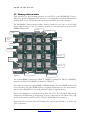
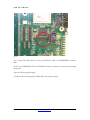
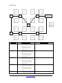
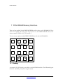
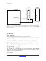
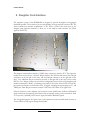
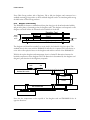
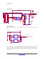
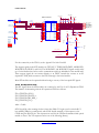
1
THE DINI GROUP
LOGIC Emulation Source
User Guide
DN8000K10
LOGIC EMULATION SOURCE
DN8000K10 User Manual Version 1
Print: February 3, 2009
© The Dini Group
7469 Draper Ave.
La Jolla, CA92037
Phone 858.454.3419 • Fax 858.454.1728
[email protected]
www.dinigroup.com
Table of Contents
CHAPTER 1:
ABOUT THIS MANUAL
1
............................................................ 9
MANUAL CONTENTS ........................................................................................................................................... 10
About this Manual ................................................................................................................................................................................. 10
Quick Start Guide ................................................................................................................................................................................. 10
Controller (USB) Software Guide ....................................................................................................................................................... 10
Board Hardware Description ............................................................................................................................................................... 10
Reference Design Guide ........................................................................................................................................................................ 10
FPGA Design Guide .............................................................................................................................................................................. 10
Ordering Information ........................................................................................................................................................................... 10
2
ADDITIONAL RESOURCES.................................................................................................................................. 10
3
CONVENTIONS ..................................................................................................................................................... 13
3.1
Typographical ............................................................................................................................................................................ 13
3.2
Content ....................................................................................................................................................................................... 13
File names ........................................................................................................................................................................... 13
3.2.1
3.2.2
Physical orientation and Origin .......................................................................................................................................... 14
3.2.3
Part Pin Names .................................................................................................................................................................... 14
3.2.4
Schematic Clippings ........................................................................................................................................................... 14
3.2.5
Media card interface............................................................................................................................................................ 14
3.2.6
Config FPGA ...................................................................................................................................................................... 14
3.2.7
Terminology ........................................................................................................................................................................ 14
3.2.8
FPGA Numbering ............................................................................................................................................................... 15
QUICK START GUIDE
.................................................................. 16
1
PROVIDED MATERIALS ....................................................................................................................................... 16
2
ESD WARNING...................................................................................................................................................... 17
3
POWER-ON INSTRUCTIONS ............................................................................................................................... 18
3.1
Check Power Jumper ................................................................................................................................................................ 18
A B O U T
T H I S
M A N U A L
3.2
Memory and heat sinks............................................................................................................................................................. 19
3.3
Prepare configuration files ....................................................................................................................................................... 20
3.4
Connect cables ........................................................................................................................................................................... 22
3.5
Power on ..................................................................................................................................................................................... 22
3.6
Check Power indicator LEDs................................................................................................................................................... 23
3.7
View configuration feedback over RS232 ............................................................................................................................... 23
Watch startup sequence over RS232 .................................................................................................................................. 23
3.7.1
3.7.2
Interactive configuration ..................................................................................................................................................... 25
3.7.3
Read temperature sensors.................................................................................................................................................... 26
3.7.4
User Serial port ................................................................................................................................................................... 27
3.8
Check LED status lights ........................................................................................................................................................... 28
4
USING THE USB CONTROLLER PROGRAM ..................................................................................................... 29
4.1
Operating the USB controller program .................................................................................................................................. 30
4.2
Using AETEST to run hardware tests .................................................................................................................................... 32
AETest on Linux or Solaris ................................................................................................................................................ 32
4.2.1
4.2.2
Use AETest ......................................................................................................................................................................... 32
5
BOARD CONTROLS ............................................................................................................................................. 35
6
MOVING ON........................................................................................................................................................... 36
CONTROLLER SOFTWARE
................................... 37
1
USB CONTROLLER .............................................................................................................................................. 37
1.1
Visual display ............................................................................................................................................................................. 38
1.2
Log window ................................................................................................................................................................................ 38
1.3
Menu Options ............................................................................................................................................................................ 38
Contextual Menu ................................................................................................................................................................. 38
1.3.1
1.3.2
File Menu ............................................................................................................................................................................ 38
1.3.3
Edit Menu ............................................................................................................................................................................ 39
1.3.4
FPGA Configuration Menu................................................................................................................................................. 39
1.3.5
FPGA Memory Menu ......................................................................................................................................................... 40
1.3.6
Settings Info ........................................................................................................................................................................ 41
1.3.7
Settings/Info Menu .............................................................................................................................................................. 43
2
AETEST ................................................................................................................................................................. 44
2.1
Running AETEST ..................................................................................................................................................................... 45
2.2
Compiling AETEST .................................................................................................................................................................. 45
DN8000K10 User Guide
www.dinigroup.com
3
A B O U T
T H I S
M A N U A L
3
UPDATING THE DN8000K10 FIRMWARE ........................................................................................................... 45
3.1
Updating the MCU (flash) firmware ....................................................................................................................................... 46
3.2
Updating the Configuration FPGA (PROM) firmware ........................................................................................................ 47
4
PROGRAMMER’S GUIDE ..................................................................................................................................... 50
4.1
Cypress CY7C68013A .............................................................................................................................................................. 51
4.2
Configuration FPGA ................................................................................................................................................................. 51
Configuration Register Map ............................................................................................................................................... 52
4.2.1
4.3
Vendor Request List ................................................................................................................................................................. 54
4.4
USB Reference Design Control ................................................................................................................................................ 55
Main Bus accesses............................................................................................................................................................... 55
4.4.1
4.4.2
Configuration ...................................................................................................................................................................... 56
4.4.3
Readback ............................................................................................................................................................................. 56
HARDWARE
..................................................................................................................... 57
1
OVERVIEW ............................................................................................................................................................ 57
2
CONFIGURATION CIRCUIT ................................................................................................................................. 58
2.1
Overview..................................................................................................................................................................................... 58
2.2
Configuration Options .............................................................................................................................................................. 59
CompactFlash ...................................................................................................................................................................... 59
2.2.1
2.2.2
Jtag....................................................................................................................................................................................... 63
2.2.3
SelectMap ............................................................................................................................................................................ 65
2.2.4
IDE (Remote Compact Flash) ............................................................................................................................................. 65
2.2.5
USB ..................................................................................................................................................................................... 66
2.3
The Configuration FPGA ......................................................................................................................................................... 66
Config FPGA Configuration ............................................................................................................................................... 66
2.3.1
2.3.2
Smart Media / Compact Flash............................................................................................................................................. 68
2.3.3
MCU communication .......................................................................................................................................................... 69
2.3.4
Clock control ....................................................................................................................................................................... 69
2.3.5
RS232 .................................................................................................................................................................................. 71
2.3.6
Main Bus control ................................................................................................................................................................. 72
2.3.7
LEDs .................................................................................................................................................................................... 72
2.3.8
Remote access ..................................................................................................................................................................... 72
2.3.9
IIC ........................................................................................................................................................................................ 72
2.3.10
Signal Descriptions ......................................................................................................................................................... 72
2.4
FPGA configuration Process .................................................................................................................................................... 72
2.5
MCU ........................................................................................................................................................................................... 75
RS232 .................................................................................................................................................................................. 75
2.5.1
2.5.2
Clocks .................................................................................................................................................................................. 76
2.5.3
LEDs .................................................................................................................................................................................... 77
2.5.4
Memory space ..................................................................................................................................................................... 77
2.5.5
Config FPGA Memory Space ............................................................................................................................................. 79
2.5.6
Flash and SRAM memory space......................................................................................................................................... 81
2.5.7
USB ..................................................................................................................................................................................... 81
U
DN8000K10 User Guide
www.dinigroup.com
4
A B O U T
2.5.8
3
T H I S
M A N U A L
CompactFlash ...................................................................................................................................................................... 84
CLOCKING ............................................................................................................................................................ 85
3.1
Global Clocks ............................................................................................................................................................................. 87
ICS 8442 Phases .................................................................................................................................................................. 88
3.1.1
3.1.2
SS (Single Step) Clocks ...................................................................................................................................................... 89
3.1.3
DIV Clocks .......................................................................................................................................................................... 90
3.1.4
User Clock ........................................................................................................................................................................... 91
3.2
Reference Clock ......................................................................................................................................................................... 92
3.3
Daughter card clocks ................................................................................................................................................................ 92
3.4
FPGA clock banks ..................................................................................................................................................................... 94
3.5
Expansion CLPD ....................................................................................................................................................................... 94
3.5.1
FX CLPD............................................................................................................................................................................. 96
4
RESET TOPOLOGY .............................................................................................................................................. 96
4.1
Reset Configuration .................................................................................................................................................................. 96
5
POWER .................................................................................................................................................................. 98
5.1
Switching power supplies ....................................................................................................................................................... 101
5.2
Secondary Power Supplies ..................................................................................................................................................... 102
DDR2 Termination Power ................................................................................................................................................ 102
5.2.1
5.2.2
MGT Power ....................................................................................................................................................................... 103
5.2.3
Optical Module Power ...................................................................................................................................................... 104
5.2.4
VBATT.............................................................................................................................................................................. 105
5.3
Power distribution ................................................................................................................................................................... 107
Bypassing .......................................................................................................................................................................... 108
5.3.1
5.3.2
VCCAUX .......................................................................................................................................................................... 108
5.4
Cooling ...................................................................................................................................................................................... 108
6
FPGA INTERCONNECT ...................................................................................................................................... 110
6.1
High speed Serdes support ..................................................................................................................................................... 110
6.2
Main Bus .................................................................................................................................................................................. 113
7
FPGA DRAM MEMORY INTERFACE ................................................................................................................. 115
7.1
Clocking .................................................................................................................................................................................... 115
7.2
Signaling ................................................................................................................................................................................... 116
Termination ....................................................................................................................................................................... 116
7.2.1
7.2.2
Source-synchronous clocking ........................................................................................................................................... 116
7.3
SODIMM Power supply ......................................................................................................................................................... 116
7.4
Alternate Memory modules.................................................................................................................................................... 117
DN8000K10 User Guide
www.dinigroup.com
5
A B O U T
8
T H I S
M A N U A L
DAUGHTER CARD INTERFACE ........................................................................................................................ 118
8.1
Daughter card Physical........................................................................................................................................................... 119
8.1.1
Daughter Card Locations .................................................................................................................................................. 119
8.1.2
Daughter card mounting.................................................................................................................................................... 120
8.1.3
Insertion and removal........................................................................................................................................................ 121
8.2
Daughter Card Electrical ....................................................................................................................................................... 122
Pin assignments ................................................................................................................................................................. 122
8.2.1
8.2.2
CC, VREF, DCI ................................................................................................................................................................ 125
8.2.3
Global clocks ..................................................................................................................................................................... 125
8.2.4
Power and Reset ................................................................................................................................................................ 125
8.2.5
MGT Signals ..................................................................................................................................................................... 126
8.2.6
VCCO Voltage .................................................................................................................................................................. 126
8.2.7
VCCO bias generation ...................................................................................................................................................... 126
8.3
Daughter card Types............................................................................................................................................................... 127
Types 1 and 2 Short (300pin & 400pin Short) ................................................................................................................. 128
8.3.1
8.3.2
Type 3 (300pin) ................................................................................................................................................................. 128
8.3.3
Type 0 (300 FX) ................................................................................................................................................................ 129
9
LEDS .................................................................................................................................................................... 129
10
MGT SERIAL RESOURCES................................................................................................................................ 134
10.1
RocketIO .............................................................................................................................................................................. 134
10.2
RocketIO signaling .............................................................................................................................................................. 135
10.3
RocketIO Clock Resources ................................................................................................................................................. 137
10.3.1
Daughter card input ....................................................................................................................................................... 137
10.3.2
Synthesizers................................................................................................................................................................... 137
10.3.3
Samtec ........................................................................................................................................................................... 138
10.3.4
Oscillators ..................................................................................................................................................................... 138
10.3.5
XFP REFCLK ............................................................................................................................................................... 143
10.4
MGT Power network .......................................................................................................................................................... 143
10.4.1
RTERM and MGTVREF .............................................................................................................................................. 145
10.4.2
FX CES2 power supplies. ............................................................................................................................................. 145
10.5
Connections .......................................................................................................................................................................... 145
10.5.1
Samtec Multi Gigabit Cable Connector ........................................................................................................................ 148
10.5.2
Optical Modules ............................................................................................................................................................ 150
10.5.3
SFP ................................................................................................................................................................................ 150
10.5.4
SFP Expansion CPLD ................................................................................................................................................... 151
10.5.5
XFP................................................................................................................................................................................ 153
10.5.6
XFP IIC ......................................................................................................................................................................... 154
10.5.7
XFP expansion CLPD ................................................................................................................................................... 154
10.5.8
The daughter card .......................................................................................................................................................... 155
10.5.9
The SMAs ..................................................................................................................................................................... 157
11
FPGA SYSTEM MONITOR/ADC ......................................................................................................................... 158
12
MECHANICAL ..................................................................................................................................................... 160
12.1
Overview. ............................................................................................................................................................................. 160
12.2
Base Plate ............................................................................................................................................................................. 160
DN8000K10 User Guide
www.dinigroup.com
6
A B O U T
13
T H I S
M A N U A L
TEST POINTS AND CONNECTORS .................................................................................................................. 162
13.1
Test points ............................................................................................................................................................................ 162
13.2
Connectors ........................................................................................................................................................................... 164
THE REFERENCE DESIGN
..................................... 168
1
EXPLORING THE REFERENCE DESIGN .......................................................................................................... 168
1.1
What is the Reference Design? .............................................................................................................................................. 168
1.2
Running the Reference Design ............................................................................................................................................... 170
The Precompiled Bit files ................................................................................................................................................. 170
1.2.1
1.2.2
Load FPGAs with the reference design ............................................................................................................................ 171
1.2.3
Run the AETest program .................................................................................................................................................. 171
1.2.4
Run the RocketIO Test ...................................................................................................................................................... 171
1.3
Compiling the Reference Design (Windows) ........................................................................................................................ 174
1.3.1
Modify Source ................................................................................................................................................................... 174
1.3.2
Xilinx ISE .......................................................................................................................................................................... 175
1.3.3
The Build Utility: Make.bat .............................................................................................................................................. 176
2
IMPLEMENTATION DETAILS ............................................................................................................................. 177
2.1
Main Test.................................................................................................................................................................................. 177
2.2
RocketIO V4 Test .................................................................................................................................................................... 179
2.3
LVDS Test ................................................................................................................................................................................ 180
Clock Summary ................................................................................................................................................................. 180
2.3.1
3
ADDRESS MAPS................................................................................................................................................. 181
3.1
Memory Space ......................................................................................................................................................................... 181
Decoder ............................................................................................................................................................................. 183
3.1.1
3.2
Main Bus Signaling ................................................................................................................................................................. 185
ORDERING INFORMATION
................................... 188
1
FPGA OPTIONS .................................................................................................................................................. 188
1.1
FPGA F0, F12 .......................................................................................................................................................................... 188
1.2
FPGA F1, F2, F3, F4, F5, F6, F7, F8, F9, F10, F11, F13, F14, F15:................................................................................... 188
1.3
Configuration FPGA: ............................................................................................................................................................. 189
2
MULTI-GIGABIT SERIAL OPTIONS ................................................................................................................... 189
DN8000K10 User Guide
www.dinigroup.com
7
A B O U T
T H I S
M A N U A L
2.1
Serial Clock Crystals............................................................................................................................................................... 189
3
OPTIONAL EQUIPMENT .................................................................................................................................... 189
3.1
Rack mount Chassis ................................................................................................................................................................ 189
3.2
Daughter cards ........................................................................................................................................................................ 190
4
THIRD PARTY EQUIPMENT ............................................................................................................................... 191
5
COMMON PROBLEMS ....................................................................................................................................... 192
5.1.1
Simulation Does not match Synthesis .............................................................................................................................. 192
5.1.2
XST is giving errors because it cannot find virtex4.v or resync.v ................................................................................... 193
5.1.3
Signal name[0] exists in my code, but place and route MAP step complains the signal name[0] from my ucf file does
not exist 193
5.1.4
Certify fails because the ports on my Virtex 4 do not match the specified part .............................................................. 193
5.1.5
The DN8000K10 cannot read my SmartMedia card. The RS232 port prints: Bad SM card format ............................... 193
5.1.6
There is a lot of deterministic jitter (DJ) on my RocketIO channel ................................................................................. 193
5.1.7
There is a lot of deterministic jitter (DJ) on my RocketIO clock signals ......................................................................... 194
5.1.8
My design works correctly in all the FPGAs except for one ........................................................................................... 194
5.1.9
RocketIO is getting a high bit error rate ........................................................................................................................... 194
5.1.10
RocketIO is not working ............................................................................................................................................... 194
5.2
Common Questions ................................................................................................................................................................. 194
5.2.1
Where are all of the debug pins ........................................................................................................................................ 194
5.2.2
Where can get the daughter card connectors? .................................................................................................................. 194
5.2.3
Can I use two Dini Products at the same time? ................................................................................................................ 194
5.2.4
Do you provide a board description file for ____? ........................................................................................................... 194
5.2.5
Where is the VHDL reference design? ............................................................................................................................. 194
DN8000K10 User Guide
www.dinigroup.com
8
1
Chapter
About this Manual
:
r1
te
p
a
h
C
Welcome to DN8000K10 Logic Emulation Board
Congratulations on your purchase of the DN8000K10 LOGIC Emulation Board. If
you are unfamiliar with Dini Group products, you should read Chapter 2, Quick Start
Guide to familiarize yourself with the user interfaces the DN8000K10 provides.
DN8000K10
A B O U T
T H I S
M A N U A L
1 Manual Contents
About this Manual
List of available documentation and resources available. Reader’s Guide to this manual
Quick Start Guide
Step-by-step instructions for powering on the DN8000K10, loading and communicating with a
simple provided FPGA design and using the board controls.
Controller (USB) Software Guide
A summary of the functionality of the provided software. Implementation details for the remote
USB board control functions and instructions for developing your own USB host software.
Board Hardware Description
Detailed description and operating instructions of each individual circuit on the DN8000K10
Reference Design Guide
Detailed description of the provided DN8000K10 reference design. Implementation details of
the reference design interaction with DN8000K10 hardware features.
FPGA Design Guide
Information needed to use the DN8000K10 with third-party software, including Xilinx ISE,
Certify, and Identify. Some commonly asked questions and problems specific to the
DN8000K10
Ordering Information
Contains a list of the available options and available optional equipment. Some suggested parts
and equipment available from third party vendors.
2 Additional Resources
For additional information, go to http://www.dinigroup.com. All of the electronic information
provided on the User CD is updated frequently; your User CD contains the latest files available
at the time your board was shipped.
Resource
DN8000K10 User
Guide
DN8000K10 User Guide
Description
This is your first source of technical information.
www.dinigroup.com
10
A B O U T
T H I S
M A N U A L
Resource
DN8000K10 User
Guide appendicies
Description
The appendicies are distributed with the User Guide on the
user CD and are available from the Dini Group website:
www.dinigroup.com
PIN_OTHER – Pin-to-pin connection information for
Daughter cards, clocks, memory modules,
Multi-gigabit transceivers (MGT), LED and
Main Bus
PIN_DIAG – Pin-to-pin connections for inter-FPGA
interconnect “Diagonal” connections.
PIN_HORIZ - Pin-to-pin connections for inter-FPGA
interconnect “Horizontal” connections.
PIN_VERT - Pin-to-pin connections for inter-FPGA
interconnect “Vertical” connections.
Schematics.pdf – Abbreviated schematics of the
DN8000K10. The PDF file can be searched
for net names and part numbers using the
PDF search.
ASSY_TOP.pdf – A drawing of the DN8000K10 top side
showing part placement
ASSY_BOT.pdf – A drawing of the DN8000K10 bottom
side, reversed, showing part placement
DRILL.pdf – A drawing showing the DN8000K10’s phystical
dimensions and mounting hole locations
DN8000K10
document library
Datasheets for all parts used on the DN8000K10,
Application notes providing implementation suggestions,
design documents, specifications of implemented interfaces
Xilinx Virtex 4 User Guide (UG70)
Xilinx RocketIO User Guide
Xilinx Virtex 4 Errata
DN8000K10 reference Example code for the DN8000K10 showing how to
design
implement memory controllers, RocketIO, etc. The design is
provided both as source, and as compiled bit file
configuration streams for use with the FPGAs installed on
your board.
Constrain (.ucf) files are included specifying pin outs, IO
standards, and location constraints. You should modify and
DN8000K10 User Guide
www.dinigroup.com
11
A B O U T
T H I S
M A N U A L
Resource
Description
use these constaint files for your own design.
Dini Group website
The web page will contain the latest manual, application
notes, FAQ, articles, and any device errata and manual
addenda. Please visit and bookmark:
http://www.dinigroup.com
E-Mail technical
support
You may direct questions and feedback to the Dini Group
using the following e-mail address:
[email protected]
Phone technical
support
Call us at 858.454.3419 during the hours of 8:00am to 5:00pm
Pacific Time.
DN8000K10 User Guide
www.dinigroup.com
12
A B O U T
T H I S
M A N U A L
3 Conventions
This document uses the following conventions. An example illustrates each convention.
3.1 Typographical
The following typographical conventions are used in this document:
Convention
Meaning or Use
Example
Courier font
Messages, prompts, and program files that the
system displays
speed grade: - 100
Courier bold
Literal commands that you enter in a syntactical
statement
ngdbuild design_name
Commands that you select from a menu
File ÆOpen
Keyboard shortcuts
Ctrl+C
Variables in a syntax statement for which you
must supply values
ngdbuild design_name
References to other manuals
See the Development System Reference Guide
for more information.
Emphasis in text
If a wire is drawn so that it overlaps the
pin of a symbol, the two nets are not
connected.
Braces [ ]
An optional entry or parameter. However, in
bus specifications, such as bus[7:0], they are
required.
ngdbuild [option_name] design_name
Braces { }
A list of items from which you must choose one
or more
lowpwr ={on|off}
Vertical bar |
Separates items in a list of choices
lowpwr ={on|off}
Vertical ellipsis
Repetitive material that has been omitted
IOB #1: Name = QOUT’
Garamond bold
Italic font
-
IOB #2: Name = CLKIN’
-
-
-
-
Horizontal ellipsis . . .
Repetitive material that has been omitted
allow block block_name
loc1 loc2 ... locn;
Prefix “0x” or suffix “h”
Indicates hexadecimal notation
Read from address 0x00110373, returned
4552494h
Letter “#” or “_n”
Signal is active low
INT# is active low
fpga_inta_n is active low
3.2 Content
3.2.1
File names
Paths to documents included on the User CD are prefixed with “D:\”. This refers to your CD
drive’s root directory.
DN8000K10 User Guide
www.dinigroup.com
13
A B O U T
3.2.2
T H I S
M A N U A L
Physical orientation and Origin
By convention, the board is oriented as show on page 3, with the “top” of the board being the
edge near FPGAs F0, F1, F2 and F3. The “bottom” is near FPGAs F12, F13, F14 anf F15. The
“right” edge is near the USB and CompactFlash sockets, the “left” side is the side with the SMA
connectors. “topside” refers to the side of the PWB with FPGAs soldered to it, “backside” is
the side with the daughtercard connectors. The reference origin of the board is the lower lefthand corner of the board.
3.2.3
Part Pin Names
3.2.4
Schematic Clippings
Pin names are given in the form XY.Z. X is one of: U for ICs, R for resistors, C for capacitors,
P or J for connectors, FB or L for inductors, TP for test points, MH for mounting structures,
FD for fiducials, BT for sockets, DS for diodes, F for fuses, HS for mechanicals, PSU for power
supply modules, Q for discreet semiconductors, RN for resistor networks, X for oscillators, Y
for crystals. Y is a number uniquely identifying each part from other parts of the same X class
on the same PWB. Z is the pin or terminal number or name, as defined in the datasheet of the
part. Datasheets for all standard and optional parts used on the DN8000K10 are included in the
Document library on the provided User CD.
Partial schematic drawings are included in this document to aid quick understanding of the
features of the DN8000K10. These clippings have been modified for clarity and brevity, and
may be missing signals, parts, net names and connections. Unmodified Schematics are included
in the User CD document library as Appendix Schematics. Please refer to this document. Use the
PDF search feature to search for nets and parts.
3.2.5
Media card interface
3.2.6
Config FPGA
There are three Media card interfaces that can be used to configure FPGAs on the
DN8000K10: CompactFlash, SmartMedia and IDE. IDE is intended to be used with a
CompactFlash-to-IDE adapter module, like the one mounted on the face panel of the optional
DN8000K10 chassis. The instructions for using all three interfaces are identical. See Hardware:
Configuration: CompactFlash section. In this manual the all of the media card interfaces are referred
to as “CompactFlash”.
Some Dini Group documentation refers to the Configuration FPGA as Spartan. The
configuration FPGA on the DN8000K10 is an LX40 or LX80 Virtex 4 FPGA.
3.2.7
Terminology
Abbreviations and pronouns are used for some commonly used phrases.
Host is the DN8000K10, as opposed to a daughter card connected to it.
MCU is the Cypress FX2 Microcontroller, U200
MGT and RocketIO are used interchangeably. MGT is multi-gigabit transceiver. RocketIO is
the Xilinx trademark on their multi gigabit transceiver hardware.
DN8000K10 User Guide
www.dinigroup.com
14
A B O U T
T H I S
M A N U A L
FPGA array include all of the 16 user-programmable Virtex 4 FPGAs on the DN8000K10.
These are F0-F15
3.2.8
FPGA Numbering
The Virtex 4 FPGAs are named from the top left in a row major order,
F0, F1, F2, F3,
F4, F5, F6, F7,
F8, F9, F10, F11,
F12, F13, F14, F15
The configuration FPGA may be referred to in some cases as F16. For historical reasons, in
some documentation, namely the reference design source code, the FPGAs may be lettered
rather than numbered, where F0 is A, F1 is B… F15 is P.
DN8000K10 User Guide
www.dinigroup.com
15
2
Chapter
Quick Start Guide
:
r2
te
p
a
h
C
The Dini Group DN8000K10 is the biggest general-purpose FPGA
system available using the Xilinx Virtex 4 FPGA. The built-in
configuration circuitry makes configuration management very easy.
However, due to the number of features and flexibility of the board, it
will take some time to become familiar with all the control and monitor
interfaces equipped on the DN8000K10. Please follow this quick start
guide to become familiar with the board before starting your logic
emulation project.
1 Provided materials
Examine the contents of your DN8000K10 kit. It should contain:
•
DN8000K10 board mounted on metal base plate
•
EPS Power supply
•
One 128MB CompactFlash card with reference design
•
USB CompactFlash/SmartMedia card reader
•
RS 232 IDC header cable to female DB9
•
6 Foot computer serial cable
•
USB cable
•
CD ROM containing
- Virtex 4 Reference Design source code and .bit files
- User manual, FPGA pin list in excel format
- Datasheets for all parts on the DN8000K10
- Board Schematic PDF
- USB controller program (usbcontroller.exe)
Q U I C K
S T A R T
G U I D E
- Reference design driver program (Aetest_usb.exe)
- Source code for USB controller program, DN8000K10 firmware, USB drivers
2 ESD Warning
The DN8000K10 is sensitive to static electricity, so treat the PCB accordingly. The target
market for this product are engineers that are familiar with FPGAs and circuit boards. However,
if needed, the following web page has an excellent tutorial on the “Fundamentals of ESD” for
those of you who are new to ESD sensitive products:
http://www.esda.org/basics/part1.cfm
The DN8000K10 is shipped in a metal carrier case designed to protect the board from physical
and electrical damage. When you handle the DN8000K10, contact the handles of the carrier to
ground yourself before touching the PWB.
The 300 and 400-pin connectors are not 5V tolerant. According to the Virtex 4 datasheets, the
maximum applied voltage to these signals is VCCO + 0.5V (3.0V while powered on). On the
DN8000K10, FPGA IO signals directly drive connectors and other exposed nets on the PWB.
Be especially careful when working with cables and connectors.
DN8000K10 User Guide
www.dinigroup.com
17
Q U I C K
S T A R T
G U I D E
3 Power-On Instructions
In the following sections, you will need to know the location of the following DN8000K10
features.
CompactFlash
SmartMedia
DDR2 SODIMM 0
USB port
RS232 P204
P203
EPS Power
Figure 1
3.1 Check Power Jumper
The DN8000K10 can be installed in an optional chassis
with a remote power-on switch. When not installed in its
chassis, the remote control connector needs to have a
jumper installed on its power-on signal. This jumper is
installed before the DN8000K10 is shipped. Check the
jumper installed in P203 pin 3 to pin 4. This jumper
connects the EPS power supply PSON signal to GND.
DN8000K10 User Guide
www.dinigroup.com
18
Q U I C K
S T A R T
G U I D E
3.2 Memory and heat sinks
There should be an active heatsink installed on each FPGA on the DN8000K10. Virtex 4
FPGAs are capable of dissipating 15W or more, so you should always run them with heat sinks
installed. There is a fan 12V power connector next to each FPGA for an active heatsink.
The DN8000K10 comes packaged without memory installed. If you want to use the Dini
Group reference design to test your memory modules, you can install them now in the 1.8V
DDR2 DIMM sockets.
DIMM 1
FPGA F2
DIMM 0
FPGA F3
FPGA F0
(“FX0”)
FPGA F1
FPGA F5
FPGA F11
FPGA F12
(“FX1”)
FPGA F15
FPGA F13
FPGA F14
DIMM 3
Figure 2
DIMM 2
The socket DIMM0 is connected to FPGA F1. DIMM1 is connected to FPGA F2. DIMM2 is
connected to FPGA F13. DIMM3 is connected to FPGA F14.
The socket can accept any capacity DDR2 SODIMM module. Note that DDR1 modules will
not work in these slots since DDR1 requires a completely different pin-out. For other memory
options for the DN8000K10, see Ordering Information: Optional Equipment: Memory.
FPGAs are numbered in a row-major order, from F0 to F15. By convention, Dini Group
references board dimensions as shown above. The top of the board is near FPGAs F0-F3 and
the left of the board is near FPGAs F0, F4, F8, F12 and the RocketIO connectors.
Since F0 and F12 are both Virtex 4 FX family parts, they are also referred to as “FX0” and
“FX1” respectively.
DN8000K10 User Guide
www.dinigroup.com
19
Q U I C K
S T A R T
G U I D E
3.3 Prepare configuration files
The DN8000K10 reads FPGA configuration data from a CompactFlash card. To program the
FPGAs on the DN8000K10, FPGA design files (with a .bit file extension) put on the root
directory of the CompactFlash card file using the provided USB media card reader. The
DN8000K10 ships with a 128MB CompactFlash card preloaded with the Dini Group reference
design. This card is labeled “DN8000K10 Ref Design”. You can skip the “prepare config files”
step if you wish. Just use the preloaded Ref Design card. Also note that there is a SmartMedia
card interface on the DN8000K10 that behaves identically to the CompactFlash interface.
1. Insert a blank 128MB CompactFlash card (provided) into your USB card reader. If you
have fewer than 16 FPGAs on your DN8000K10, you may be able to use a lower
capacity card. The only supported file system is FAT16. (This is the standard file format
for CompactFlash)
Figure 3
2. Copy a configuration stream file (with a .bit file extension generated by the Xilinx tool
bitgen) for each of the 16 Virtex 4 FPGAs on to the Compact Flash card. The compiled
.bit files of the Dini Group DN8000K10 reference design are provided on the User CD
in the directory
D:\FPGA Programming Files\Standard_Reference_Design
There are provided programming files for all types of supported FPGAs, you must
select the ones that are compiled for the FPGAs on your board.
For more information about generating configuration streams, see FPGA Design Guide
and Hardware: Configuration Section
3. Create a file on the root of the Compact Flash card called main.txt. The main.txt file
contains instructions for the configuration circuitry of the DN8000K10. It also contains
settings required by the reference design to work properly like clock frequencies and
main bus enable. See Hardware: Configuration Section: Compact Flash for a detailed
description of the available main.txt file commands.
DN8000K10 User Guide
www.dinigroup.com
20
Q U I C K
S T A R T
G U I D E
4. Copy the following text into main.txt and save. Eject the Compact Flash card.
Default Main.txt file contents:
//main.txt use with DN8000K10 reference design
verbose level: 2
sanity check: y
8442
8442
8442
8442
PH0
PH1
PH2
REF
CLOCK
CLOCK
CLOCK
CLOCK
FREQUENCY:
FREQUENCY:
FREQUENCY:
FREQUENCY:
150MHz
200MHz
66MHz
200MHz
PH2 DIVIDE BY: 2^1
GCLK0 SELECT: 8442 // 350MHz
GCLK1 SELECT: 8442 // 200MHz
GCLK2 SELECT: DIV // 66MHz / 2 = 33MHz
// configure all 16 FPGAs
FPGA 0: fpga_f0.bit
FPGA 1: fpga_f1.bit
FPGA 2: fpga_f2.bit
FPGA 3: fpga_f3.bit
FPGA 4: fpga_f4.bit
FPGA 5: fpga_f5.bit
FPGA 6: fpga_f6.bit
FPGA 7: fpga_f7.bit
FPGA 8: fpga_f8.bit
FPGA 9: fpga_f9.bit
FPGA 10: fpga_f10.bit
FPGA 11: fpga_f11.bit
FPGA 12: fpga_f12.bit
FPGA 13: fpga_f13.bit
FPGA 14: fpga_f14.bit
FPGA 15: fpga_f15.bit
DGCLK0 Select: DC0 62.5MHz// or DC1
DGCLK1 Select: DC2 250Mhz // or DC3
DGCLK2 select: DC5 // or DC6,
DGCLK3 select: DC7 // or DC8,
//end
Figure 4
5. Insert the CompactFlash card labeled “Reference Design” into the DN8000K10’s
CompactFlash (CF) slot. If the DN8000K10 is in a chassis, there is a remote CF slot on
the faceplate of the chassis.
DN8000K10 User Guide
www.dinigroup.com
21
Q U I C K
S T A R T
G U I D E
3.4 Connect cables
The configuration circuitry can accept user input to control
FPGA configuration or provide feedback during the
configuration process. The configuration circuitry IO can also
be used to transfer data to and from the user design. This can be
done over USB with the provided software, or over RS232 with
a serial port terminal.
1. Use the provided ribbon cable to connect the MCU RS232 port (P204) to a computer
serial port to view feedback from the configuration circuitry during FPGA
configuration. Using the cables provided, the red stripe on the cable indicates pin one.
Pin one is labeled “TX” on P204.
2. Run a serial terminal program on your PC. Windows XP users can use Microsoft’s
HyperTerminal
Start->Programs->Accessories->Communications->HyperTerminal
however we recommend using a good terminal program such as SecureCRT
(Vandyke.com). Make sure the computer serial port is configured with the following
options:
-Bits per second: 19200
-Data bits: 8
-Parity: None
-Stop Bits: 1
-Flow control: None
-Terminal Emulation: VT100 (or none)
3. Connect a USB cable (provided) to connect the DN8000K10 to a Windows XP
computer. Older Windowses may work, but are not supported. Use connector J203 on
the DN8000K10, or if it is installed in a chassis, you can use the remote USB power on
the faceplate of the chassis.
4. Connect power supply cables. If you are using an EPS power supply (provided) connect
all three power connectors (4, 8 and 24 pin) to P202, P201, and P200. If the
DN8000K10 is installed in its chassis, use the red power switch on the faceplate to
power on the DN8000K10. If you are operating without the chassis, a jumper must be
installed on P203 pin 3 to pin 4, or the EPS power supply will not turn on. There is no
power switch on the supplied power supply, so the DN8000K10 will power on
immediately after you plug it in. You can also use a standard ATX power supply for the
DN8000K10. See Hardware: Power
3.5 Power on
If the board is in a chassis, you can use the front panel “POWER” switch to turn on the
DN8000K10. If the board is not in a chassis you must use the power supply’s on/off switch to
control the DN8000K10 power. When using the supplied EPS power supply without the
DN8000K10 User Guide
www.dinigroup.com
22
Q U I C K
S T A R T
G U I D E
chassis, the DN8000K10 is always powered on as long as a jumper is installed on P203. Use a
wall switch or install a toggle switch on the power supply to control power.
When the DN8000K10 powers on, it automatically loads Xilinx FPGA design files (ending with
a .bit extension), found on the CompactFlash card in the CompactFlash slot into the FPGAs.
See Hardware: Configuration for a detailed description of the boot-up process.
3.6 Check Power indicator LEDs
The DN8000K10 monitors all power rails on the board for under voltage. If any of the power
supplies are not above their threshold voltages, then the board will be held in reset. Each power
rail has a green LED indicator next to the power supply generating that voltage. If your board is
held in reset, check these LEDs to see which power supply is failing. A complete list of LEDs
on the DN8000K10 is listed in the Hardware: LEDs section.
If your board is being held in reset, a ref LED, DS 17 will flash. This LED is located near the
upper right-hand side of the board.
3.7 View configuration feedback over RS232
As the DN8000K10 powers on and the configuration circuitry reads configuration instructions
from the CompactFlash card, your RS232 terminal (connected to the serial connector on the
Chassis, or directly to the connector P204) will display useful information about the
Configuration process. If your Dini Group product ever fails to configure an FPGA, this is the
best place to look for diagnostic information.
3.7.1
Watch startup sequence over RS232
The following is a capture from a successful configuration.
RS232 Output
Description of Output
-- FPGAS STUFFED -00 01 04 05
The MCU is pre-programmed with the optional equipment that is
installed on your DN8000K10.
-- 8442 INPUT FREQUENCIES -PH0: 25.0
PH1: 16.0
PH2: 14.318
FX0_0: 25.5
FX0_1: 25.0
FX1_0: 25.5
FX1_1: 25.0
CF CTRL = 0xC0
SMART MEDIA CARD DETECTED
Reading SM info
-- SMART MEDIA INFO -MAKER ID: EC
DEVICE ID: 75
SIZE: 32 MB
DN8000K10 User Guide
The MCU searches the media card slots, Compact Flash, Smart Media
and IDE (Remove chassis CompactFlash). If a media card is plugged
into one of these slots, the Configuration circuit reads the card and
follows the configuration commands on it.
If the MCU cannot detect your SmartMedia card, make sure you have
not reformatted the card using Windows. If you need to reformat a
www.dinigroup.com
23
Q U I C K
S T A R T
G U I D E
SmartMedia card, use the utility included on the user CD.
-- FILES FOUND ON SMART MEDIA CARD
FPGA_F0.BIT
FPGA_F1.BIT
FPGA_F4.BIT
FPGA_F5.BIT
MAIN~1.TXT
MAIN.TXT--
By default, the Configuration circuit reads a file named “Main.txt” on
the media card for configuration commands.
-- OPTIONS -Message level set to: 2
Sanity check option for bit files: ON
Setting 8442 PH0 CLOCK FREQUENCY to 100
M val = 0x0010 N val = 0x0004
Setting 8442 PH1 CLOCK FREQUENCY to 100
M val = 0x0019 N val = 0x0004
Setting 8442 PH2 CLOCK FREQUENCY to 100
M val = 0x001C N val = 0x0004
PH CLK DIVIDE VALUE: PH0 = 2
PH CLK DIVIDE VALUE: PH1 = 2
PH CLK DIVIDE VALUE: PH2 = 2
GCLK: 0 MUX = DIV
GCLK_MUX_SEL = 2AGCLK: 1 MUX = DIV
GCLK_MUX_SEL = 2AGCLK: 2 MUX = DIV
-- CONFIGURATION FILES -FPGA 0: FPGA_F0.BIT
FPGA 1: FPGA_F1.BIT
FPGA 4: FPGA_F4.BIT
FPGA 5: FPGA_F5.BIT
The global clocks (G0CLK, G1CLK, G2CLK, REFCLK) are
frequency-configurable. The binary sequence M represents the
multiplication applied to the installed crystal. The N represents the
division applied. See the Hardware: Clocking for details.
FPGA pin assignments for clocks are found in the appendix
PINS_OTHER
The MCU reads the configuration stream file assignments to each
FPGA.
******CONFIGURING FPGA 0************
-- Performing Sanity Check on Bit File -- BIT FILE ATTRIBUTES -FILE NAME: FPGA_F0.BIT
FILE SIZE: 00280F9A bytes
PART: 4vfx60ff1152
DATA: 2005/11/09
TIME: 19:14:01
Sanity check passed
........................................
..DONE WITH CONFIGURATION OF FPGA:
0
Before configuring an FPGA, the configuration circuit (MCU) reads
the header information in the .bit file. If the target device in the
header does not match the FPGA type on the board, the
configuration stream is rejected, and the MCU prints and error
message. This check can be disabled using the sanity check:n option.
See the Hardware:Configuration:Media card section for more
information on this command.
The MCU is configuring FPGA 0 according to instructions in
MAIN.TXT
******CONFIGURING FPGA: 1*************
-- Performing Sanity Check on Bit File -- BIT FILE ATTRIBUTES --
The MCU is configuring FPGA F1 according to instructions in
MAIN.TXT
FILE NAME: FPGA_F1.BIT
FILE SIZE: 003A943B bytes
PART: 4vlx100ff151319:42:39
DATA: 2005/11/09
TIME: 19:42:39
DN8000K10 User Guide
www.dinigroup.com
24
Q U I C K
S T A R T
G U I D E
Sanity check passed
........................................
.DONE WITH CONFIGURATION OF FPGA:
1
DN8000k10 MAIN MENU (Nov 11 2005
15:48:09)
1.) Configure FPGAs using "MAIN
.TXT"
2.) Interactive configuration menu
3.) Check configuration status
4.) Change MAIN configuration file
5.) List files on Smart Media
6.) Display Smart Media text file
z) READ FROM FLASH REGISTER
x) WRITE TO FLASH REGISTER
v) READ SECTOR
w) READ SECTORS (starting at 0)
o) SEACH FOR MB RECORD
This is the DN8000K10 main menu. A discussion of the available
commands are given later this section.
r) RESET FLASH
g.) Display FPGA Temperatures
h.) Set FPGA Temperature Alarm Threshold
ENTER SELECTION:
ν
Figure 5
You should see the DN8000K10 MCU main menu. If the reference design is loaded in the
Virtex 4 FPGAs, then you should see the above on your terminal. Try pressing 3 to see if the
configuration circuit was successful in programming the FPGAs.
ENTER SELECTION: 3
********************* CONFIGURATION STATUS *******************
FPGA 0 configured with file: FPGA_F0.BIT
FPGA 1 configured with file: FPGA_F1.BIT
FPGA 4 configured with file: FPGA_F4.BIT
FPGA 5 configured with file: FPGA_F5.BIT
Figure 6
You can verify each FPGA has been successfully configured with a design by looking at the
green LED labeled F_ DONE next to each FPGA. F0 DONE is DS46. Each green LED is lit
when the FPGA next to it is successfully configured. This LED is controlled by the DONE
signal of the Virtex 4 SelectMap interface. See the Virtex 4 User Guide.
3.7.2
Interactive configuration
You can save multiple design configuration files for each FPGA on a single CompactFlash card,
and use the serial interface’s interactive configuration menu to select which .bit file to use on
each FPGA. Select menu option 2.
-=-= INTERACTIVE CONFIGURATION MENU =-=HOLD DONES = 0x02 BITS_1 = 0x12
1) Select bit files to configure FPGA(s)
2) Set verbose level (current level = 2)
3) Enable sanity check for bit files
DN8000K10 User Guide
www.dinigroup.com
25
Q U I C K
S T A R T
G U I D E
M) Main Menu
Enter Selection: 1
CF CTRL = 0xC0
SMART MEDIA CARD DETECTED
Reading SM info
Please choose an FPGA to configure (hit Q to quit)
-=-= Select Bit File for FPGA 0 =-=-
0, 1, 4, 5: 0
0) FPGA_F0.BIT
1.) FPGA_F1.BIT
2.) FPGA_F4.BIT
3.) FPGA_F5.BIT
Q) quit
Enter selection: 0
FPGA_F0.BIT
Figure 7
From the Interactive Configuration Menu select option 1, then select a bit file on the
CompactFlash card that you would like to use for FPGA F0.
You can also automate this by writing multiple configuration .txt files with alternate
configuration settings and use the RS232 menu to select among them. DN8000K10 main menu
option
4.) Change Main Configuration File
allows this.
3.7.3
Read temperature sensors
The DN8000K10 is equipped with temperature sensors to measure and monitor the
temperature on the silicon die of the Virtex 4 FPGAs. If the internal temperature of any FPGA
increases beyond a set threshold, the FPGA will become de-configured to protect the FPGA
from potential damage, and to warn the user.
According to the Virtex 4 datasheet, the maximum recommended operating temperature of the
die is 85°C. If the DN8000K10’s FPGA monitor circuit measures by default sets its reset
threshold to 80°C.
If the DN8000K10 is resetting due to temperature overload, you can use the temperature
monitor menu to measure the current junction temperature of each FPGA.
DN8000K10 User Guide
www.dinigroup.com
26
Q U I C K
S T A R T
G U I D E
ENTER SELECTION: g
-- FPGA TEMPERATURES (Degrees Celsius [+/- 4]) -F0 29
-- Set FPGA Temperature Alarm Threshold -(degrees C, decimal values, range [1-127]): 85
Old Threshold: 80
New Threshold: 85
Threshold Updated: 85 Degrees C
Figure 8
The Virtex 4 FPGA can operate at temperatures as high as 120°C without permanently
damaging the part, although timing specifications are not guaranteed. The MCU allows you to
change the reset threshold from the default of 80°C.
More information about the temperature sensor system can be found in the Hardware: Power:
Cooling section
3.7.4
User Serial port
The DN8000K10 has four serial ports (P206, P207, P208, P209) for user use. These ports can
be accessed through the MB64B Bus. See Appendix PINS_OTHER for the pin locations of the
MB64B signals on each FPGA.
Figure 9
P1 RX
P1 TX
P2 RX
P2 TX
Signal (from provided .ucf file)
and Schematic
MB64B[63]
P206
MB64B[62]
P207
MB64B[61]
P208
MB64B[60]
P209
DN8000K10 User Guide
Header Number
www.dinigroup.com
27
Q U I C K
S T A R T
G U I D E
Remember to enable the Main Bus MB64B bus switches to access the RS232 ports from the
FPGA. The switches are enabled by default. See Hardware: Interconnect: Main Bus.
3.8 Check LED status lights
The DN8000K10 has many status LEDs to help the user confirm the status of the
configuration process.
1.
Check the Reset indicator LED located near the upper, right-hand corner of the
board, DS17. If it is flashing red, the board is in reset indicating a power failure
or a firmware problem.
2.
Check the EPS power supply voltage indication LEDs to confirm that all
externally supplied power rails of the DN8000K10 are within 5% of their
nominal voltage. From the top, these green LEDs indicate the presence of
3.3V, 12V, 5.0V, and “ATX POWER OK”. A green lit “ATX power OK”
indicates that the voltage monitor inside the EPS power supply are within
acceptable operating ranges (5V is 4.5 – 5.5V, 3.3V is 3.0-3.6V).
3.
Check the Configuration FPGA status green LEDs. These are located along the
top right corner of the board.
4.
Check the Configuration FPGA DONE status LED, DS108. This LED
indicates that the Configuration FPGA has been configured. If this LED is not
lit soon after power on, then there may be a problem with the firmware on the
DN8000K10. This LED off or blinking may indicate a problem with one of the
board’s power supplies.
5.
Check the FPGA F0 green DONE LED, DS26 to the top of FPGA F0 (If F0
is installed). This green LED is lit when FPGA F0 is configured and
operational. This light should be on if you loaded the reference design from the
CompactFlash card.
DN8000K10 User Guide
www.dinigroup.com
28
Q U I C K
6.
S T A R T
G U I D E
Check the DONE green LED for each of the 15 other FPGAs.
Figure 10
7.
Check the 4 green user LEDs on FPGA F0. If the Dini Group DN8000K10
reference design was properly loaded in the correct FPGA, then these LEDs
will be blinking.
8.
If you suspect one or more FPGAs did not configure properly, check the
configuration circuitry’s “MCU” status lights. These are red LEDs (DS81 DS82
DS83 DS84) are located near the USB connector. If there has been an error,
these four LEDs blink, indicating in binary the number of the FPGA that
caused the failure. If there has been no error, there should be two LEDs on and
two off. If there was an error, the easiest way to determine the cause of the
error is to connect a terminal to the RS232 serial “MCU” port (P204) and try to
configure again. Configuration feedback will be presented over this port.
A complete listing of LEDs and their function is found in Chapter Hardware: Test points,
LEDs and Connectors
4 Using the USB Controller program
To change settings of the DN8000K10, or to communicate with the reference design (or user
design), you can use the provided USB Controller program.
Like the RS232 interface, the USB interfaces allow configuration of the FPGAs, changing clock
and other settings. The USB program can also be used to transfer data to and from the User
design at high speed.
This section will get you started with the provided software. For detailed information about the
reference design and its USB interface, see Reference Design. For detailed information about how
the USB program operates and USB drivers, see chapter Controller Software
DN8000K10 User Guide
www.dinigroup.com
29
Q U I C K
S T A R T
G U I D E
4.1 Operating the USB controller program
Use the provided USB monitoring software to verify that the design is loaded into the FPGAs.
1. Connect the provided USB cable to your DN8000K10 and to a Windows XP
computer, either before or after the DN8000K10 has powered on.
2. When you connect the DN8000K10 via USB to your PC for the first time, Windows
XP detects the DN8000K10 and asks for a driver. The board should identify itself as a
“DiNi Prod FLASH BOOT”. When the new device detected window appears, select
the option "install from a list" -> select "search for the best driver in these locations".
Select "include the location in the search" and browse to the product CD in
“USB_Software_Applications\driver\windows_wdm\”. Select "finish"
3. After Windows installs the driver, you will be able to see the following device in the
USB section of Windows device manager: “DiniGroup DN8000K10 FLASH boot”.
4. Run the USB controller application found on the product CD in “Source
Code\USBController\USBController.exe”.
Figure 11
5. This window will appear showing the current state of the DN8000K10. Next to each
FPGA a green light will appear if that FPGA is configured successfully. The visual
feedback in the window will display which FPGAs are present, which FPGAs are
configured, the source of the globals clocks, the frequency of each global clock network at
the FPGA input pins, the state of the Main Bus switches.
DN8000K10 User Guide
www.dinigroup.com
30
Q U I C K
S T A R T
G U I D E
6. Clear an FPGA of its configuration. Right-click on the image of an FPGA to get a
contextual menu. Select Clear FPGA from the menu. The green LED on the board and in
the USB Controller window should turn off.
Figure 12
7. Now configure the FPGA using the contextual menu. Right-click on the FPGA image and
select Configure FPGA. In the Open dialog box, select the DN8000K10 reference design
from the User CD and click open.
“D:\Programming Files\Standard_Reference_Design\LX100\fpga_a.bit”
If you are configuring an LX200 or FX60 devices you should select a bit file from the
LX200 or FX60 directories instead. After a couple seconds, the USB Controller window
should show a green LED appear next to the FPGA to show that it configured
successfully.
8. The message box below the DN8000K10 graphic should display some information about
the configuration process
Done
FPGA F3 cleared successfully.
Doing a sanity check...Sanity Check passed. Configuring FPGA F3 via
USB...please wait.
File
D:\Programming Files\Standard_Reference_Design \LX100\fpga_a.bit
transferred.
Configured FPGA F3 via USB
Figure 13
1. The USB Controller program also allows you to easily configure the clock settings on
the DN8000K10. The DN8000K10 reference design requires a 48Mhz or slower clock
on GCLK2 to function properly. First, check the current clock frequencies. Select from
the menu bar
Setting and Info->Read Clock Frequencies
The message window should print frequencies for the four global clocks: GCLK0,
GCLK1, GCLK2, and REFCLK, the daughter card-sourced global clocks DC0, DC1,
DC2, DC3.
DN8000K10 User Guide
www.dinigroup.com
31
Q U I C K
S T A R T
G U I D E
2. Set GCLK2 to 50Mhz. From the menu, select
Settings and Info->Set Global Clock Frequency
From the dialog box, select GCLK2, and type in 48 in the frequency box.
The USB controller program will calculate the PLL settings required to obtain the
closest achievable frequency to 48Mhz using the clocking resources available.
3. Reset the reference design. Since we have changed settings, we should send a logic reset
to the FPGA designs. You can do this from the USB Controller program. From the
menu, select
FPGA Configuration->Reset Logic
This menu option will assert the RESET_FPGA# signal to each FPGA. See the
Appendix Pins Other for the connection of this signal.
More details about each available function of the USB Controller software is found in the USB
Software Chapter.
4.2 Using AETEST to run hardware tests
In addition to the Windows GUI application, the Dini Group provides a command line
interface program that provides the same functions. If you will be using Linux or if you plan to
write your own USB software driver, you will be using the source code for this program as a
reference.
AETest is the program that you can use to verify the hardware on the DN8000K10, as well as
to demonstrate the reference design function. The following instructions assume you have a PC
running the Windows XP operating system. The user CD includes a compiled Windows version
of the AETest program. Connect the DN8000K10 to your Windows XP computer with a USB
cable and use aetest_usb in D:\Source Code\USB_Software\aetest_usb\aeusb_wdm.exe. If the
computer asks for a driver, click “Have Disk” and browse to
D:\Source Code\USB_Software\driver\win_wdm\dndevusb.inf
Dini Group does all of its development on Windows XP.
4.2.1
AETest on Linux or Solaris
To use the AETest application on Linux or Solaris, you must compile the source code included
on the User CD. Instructions for compiling AETest are found in Chapter USB Software.
To install the AETest drivers on Linux, <JACK>
4.2.2
Use AETest
The AETest_usb application is compatible with other Dini Group products, and so before
displaying its main menu it displays some USB debug information.
DN8000K10 User Guide
www.dinigroup.com
32
Q U I C K
S T A R T
G U I D E
Figure 14
The AETest application then displays its main menu.
Figure 15
Select menu option 2) to interact with the “main bus” interface of the Dini Group DN8000K10
reference design.
DN8000K10 User Guide
www.dinigroup.com
33
Q U I C K
S T A R T
G U I D E
Figure 16
The Main Bus menu will only work properly when the Dini Group reference design is loaded,
or if your user design has implemented a compatible controller.
Select Option
3) MainBus Write/Read DWORD
0x1000_0000 is address 0 of the DDR2 memory attached to FPGA F1. Enter that address and
a data pattern. AETest_usb should report back that it read back the test value. This test will only
pass if there is a DDR2 SODIMM installed in DIMM0 and the reference design, including
required clock settings, is loaded.
Menu option
5) MainBus Display
dumps 16, 32-bit words from the reference design memory space to the screen.
Enter option M) to return to the main menu.
The AETest_usb application can also be used to configure FPGAs over USB.
DN8000K10 User Guide
www.dinigroup.com
34
Q U I C K
S T A R T
G U I D E
Figure 17
Select option
4) Configure FPGA individually via USB
AETest_usb will ask for the path to a configuration .bit file, and an FPGA number to configure.
Select a .bit file from the user CD.
5 Board Controls
The DN8000K10 is designed to be operated remotely via the chassis front panel to protect your
hardware investment. As a result, the DN8000K10 has very few controls located on the PWB
itself.
Hard Reset
Soft Reset
Figure 18
DN8000K10 User Guide
www.dinigroup.com
35
Q U I C K
S T A R T
G U I D E
Press the Hard Reset button. You will see all of the 16 Virtex 4 FPGAs immediately become
un-configured. This behavior is exactly the same as if the board were powered off and back on.
When you let go of the button, the configuration circuitry will read the CompactFlash card again
and attempt to configure the FPGAs.
After the FPGAs are again configured, press and hold the Soft Reset button. You will notice
that the blinking LEDs controlled by the reference design will stop blinking. This is because the
Soft reset button causes the 16 Virtex 4 FPGAs to receive the FPGA_RESETn signal (active
low). This is the signal that the reference design uses to reset its internal logic.
CompactFlash slot
Hard Reset
Power Switch
Soft Reset
USB Port
RS232 Ports
If you have the DN8000K10 installed in the DN8000K10 Chassis, you can also use the front
panel buttons to the same effect.
6 Moving On
Congratulations! You have just configured FPGAs on the DN8000K10 and used all of the
configuration control interfaces that you must know to start your emulation project. You should
use Appendix PINS to create your design constraint (.ucf) files, or you can just use the .ucf files
that were included as part of the reference design. All of the source code for the reference
design in Verilog is included on the provided CD.
DN8000K10 User Guide
www.dinigroup.com
36
3
Chapter
Controller Software
:
r3
te
p
a
h
C
1
USB Controller
USB Controller application is used to communicate with the DN8000K10.
All USB Controller source code is included on the CD-ROM shipped with the DN8000K10.
The USB Controller can be installed on Windows 2000/3/XP. Linux and Solaris users must
use the command line interface version, AEtest_usb.
The USB Controller Application contains the following functionality:
o Verify Configuration Status
o Configure FPGA(s) over USB
o Configure FPGAs via SmartMedia card
o Clear FPGA(s)
o Reset FPGA(s)
o Set Global clocks frequency
o Set RocketIO CLK Frequency
o Update MCU FLASH firmware
The following are designed to work with Dini Group’s reference Design.
o Read/Write to FPGA(s)
o Test DDRs/Reigsters/FPGA Interconnect/Rocket IO
Before shipping a DN8000K10, the Dini Group uses this program to test all of the IO signals,
memory interfaces, serial interfaces, clocks, and connectors of your board. The program is
compatible with all Dini Group products in the 5000K, 6000K, 7000K and 8000K series
products.
U S B
S O F T W A R E
1.1 Visual display
The main window of the Dini Group USB Controller program shows the DN8000K10
Graphic.
RS232 Controls
Menu Bar
Refresh Button
Frequency Display
DN8000K10
Graphic
FPGA DONE
LED
Log Window
1.2 Log window
1.3 Menu Options
All of the menu commands available in the USB Controller program can also be set using the
CompactFlash card or RS232 interfaces. The details about the implementation of each of the
commands available is listed in the Chapter Hardware, section CompactFlash. Note that there is
a SmartMedia card interface that behaves identically to the CompactFlash interface. Both of
these interfaces are referred to in this section as “CompactFlash”.
1.3.1
Contextual Menu
Right-click on one of the images of the FPGAs to display the FPGA contextual menu. From
this menu you can configure and clear FPGAs. The FPGA image that you click determines
which FPGA is selected.
a. Configure FPGA Fn
This menu option allows you to select a configuration stream (.bit file) in an
Open dialog box. The selected FPGA n will be programmed with that stream.
b. Clear FPGA Fn
Choosing this menu item causes the selected FPGA n to become unconfigured.
1.3.2
File Menu
The File Menu has the following 1 option:
DN8000K10 User Guide
www.dinigroup.com
38
U S B
S O F T W A R E
c. Exit
Closes the USB Controller application
1.3.3
Edit Menu
The Edit Menu performs the basic edit commands on the command log in the bottom half of
the USB Controller window.
1.3.4
FPGA Configuration Menu
The FPGA Configuration Menu has the following options:
a. Refresh
This menu item refreshed the image displaying the DN8000K10 with the
current configured status of each FPGA, the main bus switch settings and
current global clock frequency values.
b. Configure via USB (individually)
After selecting this item, a window will appear and ask which FPGA you
want to configure and then which configuration stream (.bit file) you want
to configure the selected FPGA with from your computer’s file system.
The status of the FPGA configuration process will be logged in the log
window and the DN8000K10 image and clock frequencies will be updated
after the .bit file has been transferred.
c. Configure via USB using file
This option allows the user to configure more than one FPGA over USB at
a time. To use this option you must create a setup file that contains
information on which FPGA(s) should be configured and which .bit files
should be used for each FPGA. The file should be in the following format:
The first two characters of each line represents which FPGA you want
configured (F0 – F15), this letter should be followed by a colon and then
the path to the .bit file to use for this FPGA. The path to the bit file is
relative to the directory where this setup file is, or you can use the full path.
Below is an example of an accepted setup file:
F0: fpga_zero.bit
F1: ../fpga_one.bit
D:\FPGA
Programming\Files\Standard_Reference_Design\LX200\fpga_F15.bit
d. Configure via SmartMedia/CompactFlash Card
This option causes the DN8000K10 to go through its startup sequence by
reading configuration instructions from the CompactFlash card. The
Section Hardware: Configuration: CompactFlash contains instructions for
creating a configuration CF card.
DN8000K10 User Guide
www.dinigroup.com
39
U S B
S O F T W A R E
e. Clear All FPGAs
This option will immediately un-configure all FPGAs.
f. Reset
This options sends an active low reset (active for 1ms) to all FPGAs on the
signal RESET_FPGAn. Check Appendix Pins Other for the FPGA-side pin
out of these signals.
1.3.5
FPGA Memory Menu
This menu contains commands designed to work with the DN8000K10 reference design. All of
the commands in this menu cause read and write instructions to happen over the reference
design’s main bus interface. Status and control registers for the reference design are all memorymapped over this main bus interface. For a description of the main bus interface and memory
map, see the chapter Reference Design.
a. Write DWORD
Displays a dialog box that allows you to send data to a signal address in the
reference design’s address space. This operation occurs over the “main bus”
interface. See the Chapter Reference Design.
b. Read DWORD
Displays a dialog box that allows you to read data from a signal address in the
reference design’s address space. This operation occurs over the “main bus”
interface. See the Chapter Reference Design.
c. Write and Read DWORD
This displays a dialog box that tests the “main bus” interface by writing a value
to a location in the reference design’s memory space and immediately reading
that address back.
d. Test Address Space
This item shows a dialog box allowing you to test a range of locations in the
memory space of the reference design. This is used to test memory connected
to individual FPGAs that is mapped to the reference design’s “main bus”
interface.
e. Display Address Space
This item dumps a range of addresses in the reference design’s “main bus” to
the log window under the DN8000K10 image.
f. Test DDR (may be called “Test DN8000K10/PCI DDR”)
This item automates a test of the memory space on the “main bus” interface
that the reference design maps to DDR2 memory.
DN8000K10 User Guide
www.dinigroup.com
40
U S B
S O F T W A R E
g. Test DDR single FPGA (may be called “Test DN8000K10/PCI DDR”)
This item automates a test of the memory space on the “main bus” interface
but allows you to specify which FPGA(s) you would like to test.
h. Set DDR config
This item allows you to set the size of the installed DDR2 memory module.
(and hence the address range to test)
i.
Read DDR config
This item displays the current size of the installed DDR2 memory module.
j.
Display Memory Map
This item displays for reference a table showing the memory map of the default
Dini Group reference design.
k. Send Command File
This item allows the user to select a script containing “main bus” transactions to
automate testing tasks. The menu item displays an Open dialog and asks the
user to select a file. The contents of the file should be ASCII text
AD 00000000 // sets current address to 0
WR 12345678 // writes hex 12 34 56 78 to address 0
WR 12345678 // writes hex 12 34 56 78 to address 1
RD 1000 // writes 1000 DWORDs (4 byte) to log window
1.3.6
Settings Info
a.
Set RocketIO Frequency
This item shows a dialog box that allows you to set the clock source and
PLL settings of the MGT clocks. The clocks FX0_0 and FX0_1 feed the
MGTs of FPGA F0. The clocks FX1_0 and FX1_1 feed the MGTs on
FPGA F12.
b.
Set Clock input frequency
The DN8000K10 firmware is preprogrammed knowing the frequency of
the reference crystals installed on the inputs of the PLL circuits on the
board. These numbers can be overwritten using this menu option if you
have removed these crystals and replaced them with a different frequency
crystal.
c.
FPGA stuffing information
The DN8000K10 firmware comes pre-programmed with information
about the optional equipment that is installed on your board. This menu
item reads back that information and displays it.
DN8000K10 User Guide
www.dinigroup.com
41
U S B
S O F T W A R E
d.
Turn Fans On/Off
The fans on the DN8000K10 cannot be turned off. This menu item cannot
be enabled.
e.
MCU firmware version
This menu item reads back the firmware version of the MCU to help the
Dini Group debugging.
f.
Spartan version
This menu item reads back the firmware version of the Configuration
FPGA to aid the Dini Group debugging.
g.
DN8000K10 MB Switch Setup
This menu item allows the user to change the MB80B and MB64B bus
switch settings. These busses can be used as global interconnect between all
16 FPGAs, or they can be disconnected by selecting MB Switch settings to
form lower fan-out regional busses. This selection can be made with a bytewide resolution. For a description of the MB80B and MB64B busses, see
Chapter Harware: Interconnect: Main Bus.
h.
DN8000K10 MB Switch Read
This menu item displays the current state of the MB switches.
i.
DN8000K10 Global Clock Synth. Setup
This menu item allows the user to select the source of the 8 board-global
scope clock networks on the DN8000K10. The user can also change the
PLL frequency settings of the networks that have PLLs. See section
Hardware: Clocks for details.
j.
DN8000K10 Global Clock Setup Read
This option reads back the current clock settings.
k.
DN8000K10 Set N dividers
l.
DN8000K10 Read N dividers
m.
Set Phase Muxes
n.
Calculate GCLK Freq.s
This menu item measures and displays the clock frequencies of each of the
8 board-global scope clock networks on the DN8000K10. These
measurements will differ slightly from the calculated values.
o.
DN8000K10/PCI interconnect test
This menu runs an automated connectivity test of the inter-FPGA
interconnect on the DN8000K10.
DN8000K10 User Guide
www.dinigroup.com
42
U S B
S O F T W A R E
p.
1.3.7
DN8000K10/PCI interconnect Menu
This menu is used for operating the inter-FPGA interconnect
characterization test. This test is designed to operate at 350Mhz. The
following sub-menu options are available:
Display Registers AB -?
Display Registers BC -?
Reset TX -?
Reset RX -?
Restart test -?
Settings/Info Menu
The Settings/Info Menu has the following options
(1) Set FPGA RocketIO CLK Frequency
When the DN8000K10 is first powered up the RocketIO Synthesizer MGTCLK inputs
to the FPGAs are inactive, unless programmed using the main.txt file on a
CompactFlash card. (The Epson Oscillators are active.) This menu option allows the
user to specify what frequency the RocketIO Synthesizers should supply to each FPGA.
The supported frequency range is 103MHz – 260MHz. After selecting this option, a
pop-up window will ask which FPGA’s RocketIO Frequency you want to set (or you
can choose to set all to the same frequency), and then what frequency you want. The
USB Controller program will calculate the best PLL settings to achieve this output
frequency. Check the log window to verify what frequency the synthesizers were
actually set at.
(2) Set Global clock frequencies
The clocks on the DN8000K10 are automatically adjusted to the user’s desired
frequency by reading the setup file on the CompactFlash card. If you wish to change the
frequency after power-on, or do not want to use a CF card, you can set the frequency in
the USB program.
GCLK0) GCLK0 is generated from a 25MHz crystal. Possible output frequencies
are:
31.25
59.375
93.75
156.25
262.5
425
675
34.375
62.5
100
162.5
275
450
700
37.5
65.625
106.25
168.75
287.5
475
40.625
68.75
112.5
175
300
500
43.75
71.875
118.75
187.5
312.5
525
46.875
75
125
200
325
550
50
78.125
131.25
212.5
337.5
575
53.125
81.25
137.5
225
350
600
56.25
84.375
143.75
237.5
375
625
87.5
150
250
400
650
GCLK1) GCLK1 is generated from a 14.318 MHz crystal. Possible output
frequencies are:
DN8000K10 User Guide
www.dinigroup.com
43
U S B
S O F T W A R E
32.22
50.11
68.01
85.91
121.7
157.5
214.8
286.4
372.3
515.4
658.6
GCLK2)
are:
32
52
72
96
136
176
256
336
464
624
34.01
51.90
69.80
89.49
125.3
161.1
221.9
293.5
386.6
529.8
672.9
35.80
53.69
71.59
93.07
128.9
164.7
229.1
300.7
400.9
544.1
687.3
37.58
55.48
73.38
96.65
132.4
168.2
236.2
307.8
415.2
558.4
39.37
57.27
75.17
100.2
136.0
171.8
243.4
315.0
429.5
572.7
41.16
59.06
76.96
103.8
139.6
179.0
250.6
322.2
443.9
587.0
42.95
60.85
78.75
107.4
143.2
186.1
257.7
329.3
458.2
601.4
44.74
62.64
80.54
111.0
146.8
193.3
264.9
336.5
472.5
615.7
46.53
64.43
82.33
114.5
150.3
200.5
272.0
343.6
486.8
630.0
48.32
66.22
84.12
118.1
153.9
207.6
279.2
358.0
501.1
644.3
GCLK2 is generated from a 16.0 crystal. Possible output frequencies
34
54
74
100
140
184
264
336
480
640
36
56
76
104
144
192
272
344
496
656
38
58
78
108
148
200
280
352
512
672
40
60
80
112
152
208
288
368
528
688
42
62
82
116
156
216
296
384
544
44
64
84
120
160
224
304
400
560
46
66
86
124
164
232
312
416
576
48
68
88
128
168
240
320
432
592
50
70
92
132
172
248
328
448
608
RefClk) RefClk is generated from a 25.0 MHz crystal. Possible output frequencies
are the same as GCLK0
(3) FPGA Stuffing Information – This option will display the type of FPGAs that are
stuffed on the DN8000K10.
(4) MCU Firmware Version – This option will display the MCU Firmware version in the
log window.
(5) Hardware/Firmware Version – This option will display the Board Version along with
the Configuration Fpga version.
2 AETest
The AETEST utility program contains the following tests:
•
Memory Tests (DDR2)
•
Daughter Card Test
DN8000K10 User Guide
www.dinigroup.com
44
U S B
S O F T W A R E
•
BAR Memory Range Tests
•
RocketIO error rate test
•
FPGA interconnect error rate test
•
Clock frequency readback
2.1 Running AETEST
AETest_usb.exe is a Windows executable distributed on the user CD ROM. The program can
be run in Windows XP.
For the windows version of AETest, a usb driver is required. The driver can be found on the
user CD. Dndev.inf. There is no "driver" for linux USB. The Linux version of the usb software
runs in user mode. Just run the aetest application aeusb_linux.
2.2 Compiling AETEST
The source for the USB version is found on the User CD
D:\Source Code\USB_Software\aetest_usb
A Make file is provided for compiling on Linux, Solaris, Windows XP, and DOS. To compile,
open Make file and change the line
#DESTOS = LINUX
to
DETOS=LINUX
to target Linux, change
#DESTOS = WIN_WDM
to target windows XP.
Targeting Windows XP required Microsoft Visual Studio 5. Targeting DOS requires DJGPP.
3
Updating the DN8000K10 Firmware
Dini Group may release firmware bug fixes or added features to the DN8000K10. If a firmware
update is released you will need to follow the instructions in this chapter.
There are two firmware files that Dini Group may release; the first is a Micro controller (MCU)
software update that is stored in a flash memory. This update can be accomplished easily from
within the USB Controller application.
The second update that may be required is a Configuration FGPA core update. The
configuration data for the Config FPGA is contained in a Xilinx configuration PROM. This
update can be accomplished with the Xilinx JTAG programming program, Impact. You will
need a JTAG cable like Xilinx Parallel cable IV, or platform USB cable.
DN8000K10 User Guide
www.dinigroup.com
45
U S B
S O F T W A R E
3.1 Updating the MCU (flash) firmware
To protect against accidental erasure, the MCU firmware cannot be updated unless the board is
put in firmware update mode during power-on. Find Switch block 1 (S1) on the DN8000K10.
Move switch S1 #1 to the ON position. Power on the DN8000K10.
Open the USBController program. If the DN8000K10 powered on in firmware update mode,
there will be an update flash dialog box as figure on left. Click “Yes” to open flash_flp.hex file.
DN8000K10 User Guide
www.dinigroup.com
46
U S B
S O F T W A R E
If the USBController is already opened, click “Refresh” button, there will be an “Update Flash”
button near the top of the USBController window. Click on this button (as figure below).
When the Open… dialog box appears, navigate to the Firmware image file supplied by Dini
Group. The file name should be “flash_flp.hex”. Press OK.
The USB Controller should freeze for about 10 seconds while the firmware update is taking
place. When the download is complete, the Log window should print, “Update Complete”
Move Switch block S1 #1 to the OFF position to put the DN8000K10 back into normal
operation mode. Power cycle the board.
3.2 Updating the Configuration FPGA (PROM) firmware
Connect a Xilinx Parallel IV, or Platform USB configuration cable to the parallel port of your
computer. The Parallel IV cable requires external power to operate, so you may need to connect
the keyboard connector power adapter. When the Parallel IV cable has power, the status LED
on Parallel IV turns amber.
DN8000K10 User Guide
www.dinigroup.com
47
U S B
S O F T W A R E
Figure 19
Use a 14-pin 2mm IDC cable to connect the Parallel IV cable to the DN8000K10 connector
J208.
Power on the DN8000K10. When the Parallel IV cable is connected to a header, the status light
turns green.
Open the Xilinx program Impact.
(Usually found at Start>programs>Xilinx ISE>Accessories>impact)
DN8000K10 User Guide
www.dinigroup.com
48
U S B
S O F T W A R E
Figure 20
Impact may ask you to open an impact project. Hit cancel.
Choose the menu option File>Initialize Chain
Impact should detect 2 devices in the JTAG chain xcf32p and xc4vlx80. For each item in the
chain Impact will direct you to select a programming file for each. For the xcf32p device, select
the Configuration FPGA Firmware update file provided by Dini Group. This file should be
named prom_flp.mcs. Hit Open. Impact will then ask for a programming file to program the
xc4vlx80. Press Bypass.
To program the prom, right-click on the prom and select "Program…" from the popup menu.
In the options dialog that follows, the options “Erase before programming” should be selected,
and “Verify” should be deselected. Press OK. The programming process takes about 2 minutes
over the parallel port.
DN8000K10 User Guide
www.dinigroup.com
49
U S B
S O F T W A R E
Figure 21
Power cycle the DN8000K10. The new firmware is now loaded. You can close Impact and
disconnect the Parallel IV or Platform USB cable.
4 Programmer’s Guide
This section contains information to help the development of your own USB software for use
with the DN8000K10. If you do not need to develop you own USB control software, or modify
the Dini Group USB controller, you can skip this section. All of the code for AETest and USB
Controller is provided on the user CD. Precompiled Windows drivers are also provided for
Windows XP. You should also read the section Hardware: Configuration Section before attempting
to modify the USB software.
The source code for the Windows version of the USB Controller is provided in
D:\Source Code\USB_Software\USBController
as a Microsoft Visual Studio 5 project. Visual Studio 5 or later is required to compile this
program.
DN8000K10 User Guide
www.dinigroup.com
50
U S B
S O F T W A R E
4.1 Cypress CY7C68013A
A Cypress Microcontroller (MCU) with built-in USB support provides the USB interface of the
DN8000K10. All communication with the DN8000K10 over USB is initiated by the host (PC)
and consists either of a USB vendor request (See USB specification and Cypress datasheet) or a
USB bulk transfer.
Vendor requests can contain short (512Byte) messages in either direction, and cause the MCU
to execute code. In response to most vendor requests, the MCU will modify or read values in
the Configuration memory space (see next section).
Since vendor requests can contain only a limited amount of data, USB Bulk transfers are used to
send configuration data to the DN8000K10. The MCU is too slow to process USB 2.0 data at
full speed, and so the bulk transfer data is sent to external pins on the Cypress MCU (see
Cypress datasheet) and to the configuration FPGA (next section). Currently, this data is only
used to configure FPGAs, and so the data is sent to the SelectMap pins of the Virtex 4 FPGAs.
To begin communication with the DN8000K10, the USB Controller program creates a USB
connection object in the host operating system, by opening Vendor ID 0x1234 product ID
0x1234. (For the purposes of updating the firmware, the DN8000K10 can come up in
“EPROM” mode, where it loads a program capable of connecting over USB to a host,
downloading firmware and writing it to the MCU flash memory, U201. The check the MCU
makes on reset to determine which mode it should start in is the firmware update switch, S1 #4.
This EPROM code is stored in the EPROM DIP installed in U203. When the MCU is in this
mode, it registers itself to the operating system as Vendor ID 0x1234, product ID 0x1233. For
firmware update instructions, see USB Software: Firmware Update. For information about the
MCU boot up sequence, see Hardware: Configuration Circuit: MCU)
The source code for the MCU firmware (“Flash”) is provided in
D:\Source Code\MCU\FLASH
as a Keil Studios MicroVision 2.11 project file.
4.2 Configuration FPGA
The MCU unit controls all of the configuration circuits on the DN8000K10, but it does not
have sufficient IO to access all of the configuration signals. For IO expansion, the MCU’s
external memory bus is connected to a Virtex 4 LX40 FPGA. This FPGA provides a memorymapped interface to all of its IO. This bus is called the ‘Config Bus’.
The configuration FPGA is connected to all of the configuration signals of the Virtex 4 FPGAs,
the temperature sensors, status LEDs, SmartMedia card, CompactFlash card, reset buttons,
Main Bus switches, RS232 ports, clock synthesizer control signals, global clock multiplexer
control signals, FPGA clock inputs, the Main Bus, and an 300-pin expansion header.
The source code for the Configuration FPGA is provided in
D:\Source Code\ConfigFPGA
DN8000K10 User Guide
www.dinigroup.com
51
U S B
S O F T W A R E
This project can be compiled using Xilinx ISE version 7.1i SP4 or later. Your board may have
been build using an LX80 FF1148 or an LX40 FF1148 for the configuration FPGA.
4.2.1
Configuration Register Map
The DN8000K10 firmware is updated constantly to add compatibility for new products and add
features. The information in this section may change after this manual is printed. The memory
space of the MCU is 16 bits wide.
This table describes registers within the Configuration FPGA that are accessible from the
memory space of the MCU.
Address Range
Name
Description
Code Space
0x0000-0x1FFFF
EEPROM
0x2000-0xFFFFF
XDATA
XXXX-XXXX
FLASH
SRAM
0xDF10
FPGA_BE
0x DF11
FPGA_RD_DATA
// select byte in addr, read, and data bytes
0x DF12
FPGA_WR_DATA
0x DF13
0x DF14
FPGA_ADDR
FPGA_ERROR
0x DF20
0x DF21
0x DF22
GPIF_DATA
GPIF_ERROR
HOLD_DONES
0x DF23
STATES
0x DF24
0x DF25
0x DF26
0x DF27
FPGA_FREQ_H
FPGA_FREQ_SEL
FPGA_FREQ_L
MCU_STUFFING1
0x DF28
MCU_STUFFING2
0x DF29
SERIAL_SCLK
0x DF30
SERIAL_CLK_CTRL_1
0x DF36
MB80_1_CTRL0
This register holds the output values of the Main Bus
switches for MB80B, section 1. See Hardware:
Interconnect: Main Bus for the effect of this. Each bit
enables or disables 8 bits of the Main Bus
0x DF37
MB80_1_CTRL1
This register holds the output values of the Main Bus
switches for MB80B, section 1. See Hardware:
Interconnect: Main Bus for the effect of this. Each bit
enables or disables 8 bits of the Main Bus
DN8000K10 User Guide
This register contains an error code after a Main Bus
transaction
This register (1bit) determines if the FPGAs should
be held in reset until all FPGAs are configured
The state of the state machines in the Configuration
FPGA that control FPGA configuration
[7:4]= PIF_STATE, [3:0] = FPGA_STATE
This register contains a code representing the type of
FPGA installed in F0-F7
This register contains a code representing the type of
FPGA installed in F8-F15
This register (1 bit) controls the SCLK output
connected to the clock synthesizers on the
DN8000K10
This register controls the control outputs connected
to all of the clock synthesizers on the DN8000K10
www.dinigroup.com
52
U S B
S O F T W A R E
0x DF38
MB80_2_CTRL0
This register holds the output values of the Main Bus
switches for MB80B, section 2. See Hardware:
Interconnect: Main Bus for the effect of this. Each bit
enables or disables 8 bits of the Main Bus
0x DF39
FPGA_COMMUNICATION
0x DF40
MB80_2_CTRL1
This register (1 bit) set enables access to the “Internal
Main” registers (below). This register should be set to
0 when the INTERNAL_MAIN registers are not
being accessed, or when accessing address space
within the 16 user FPGAs.
This register holds the output values of the Main Bus
switches for MB80B, section 2. See Hardware:
Interconnect: Main Bus for the effect of this. Each bit
enables or disables 8 bits of the Main Bus
0x DF41
MB64_1_CTRL
0x DF42
MB64_2_CTRL
0x DF43
MB64_3_CTRL
0x DF44
0x DF45
CPLD_CS_N_CTRL
CPLD_DATA
0x DF46
CPLD_ADDR
0x DF47
GCLK_MSEL_CTRL
Holds the temporary multiplication value that will be
sent over the 2-wire bus to the selected global clock
synthesizer the next time clocks are set.
0x DF48
FPGA_PH0_DVAL
0x DF49
FPGA_PH1_DVAL
0x DF50
FPGA_PH2_DVAL
Holds the division value that the FPGA should apply
to the PH0 clock to generate the PH0 DIV output.
Holds the division value that the FPGA should apply
to the PH1 clock to generate the PH0 DIV output.
Holds the division value that the FPGA should apply
to the PH2 clock to generate the PH0 DIV output.
0x DFE
INTERNAL MAIN
Main Bus address
CF_REG_OFFSET
0x0002
REG_IDCODE
0x0004
REG_SCRATCH
0x 05
REG_HEADERTEST
0x 06
REG_HEADERTEST_STATUS1
0x 07
REG_HEADERTEST_STATUS2
0x 08
REG_HEADERTEST_STATUS3
0x 09
REG_HEADERTEST_STATUS4
0x 0A
REG_HEADERTEST_STATUS5
0x 0B
REG_HEADERTEST_STATUS6
0x 0C
REG_HEADERTEST_STATUS7
This register holds the output values of the Main Bus
switches for MB64B, section 1. See Hardware:
Interconnect: Main Bus for the effect of this. Each bit
enables or disables 8 bits of the Main Bus
This register holds the output values of the Main Bus
switches for MB64B, section 2. See Hardware:
Interconnect: Main Bus for the effect of this. Each bit
enables or disables 8 bits of the Main Bus
This register holds the output values of the Main Bus
switches for MB64B, section 3. See Hardware:
Interconnect: Main Bus for the effect of this. Each bit
enables or disables 8 bits of the Main Bus
This holds the (_ bit) value that will be sent to the
selected CPLD. See Hardware: CPLD chain
This holds the address of the selected register in the
CPLD chain. The address also determines which
CPLD is selected. See Hardware: CPLD
The Registers in the “Internal Main” interface are
accessible from the Main Bus interface. See Reference
Design. These registers must be enabled by setting the
FPGA_COMMUNICATION register (above)
DN8000K10 User Guide
This register returns a known value so the USB
Controller program can identify it as the Dini Group
reference design.
www.dinigroup.com
53
U S B
S O F T W A R E
0x 0D
REG_CLOCKCOUNT_GCLK0
This register contains the maximum value of a
counter clocked from GCLK0. The counter is reset
every 0x1000 clock cycles of CLK48
0x 0E
REG_CLOCKCOUNT_GCLK1
0x 0F
REG_CLOCKCOUNT_GCLK2
0x 10
REG_CLOCKCOUNT_GCLK3
This register contains the maximum value of a
counter clocked from GCLK1. The counter is reset
every 0x1000 clock cycles of CLK48
This register contains the maximum value of a
counter clocked from GCLK2. The counter is reset
every 0x1000 clock cycles of CLK48
This register contains the maximum value of a
counter clocked from REFCLK. The counter is reset
every 0x1000 clock cycles of CLK48
0x 11
REG_CLOCKCOUNT_GCA
0x 12
REG_CLOCKCOUNT_GCB
0x 13
REG_CLOCKCOUNT_GCC
0x 14
REG_CLOCKCOUNT_MBCLK
4.3 Vendor Request List
The USB Program is updated constantly to add compatibility to new products and to add
features. There may be changes to the application after this manual is printed that affect this
section.
The following table describes the USB interface presented to the host by the MCU
microcontroller. The USB Device identification numbers are Vendor: 0x1234, Device: 0x1234.
Vendor Request Name
VR_UPLOAD
VR_DOWNLOAD
VR_ANCHOR_DLD
VR_EEPROM
VR_RAM
VR_SETI2CADDR
VR_GETI2C_TYPE
VR_GET_FLASH_REV
VR_GET_FPGA_INFO
VR_RENUM
VR_DB_FX
VR_I2C_100
VR_I2C_400
VR_NOSDPAUTO
VR_REBOOT
VR_FLASH_ERASE
VR_CONFIG
VR_FLASH_ACCESS
VR_FLASH_SECTOR_ERASE
VR_FLASH_VERSION
VR_DISPLAY_FPGA_INFO
VR_CHECK_FPGA_INFO
VR_CHECK_FPGA_CONFIG
VR_PPC_RS232
FLASH_VERSION_ADDR
VR_SET_EP6TC
ID Code
0xc0
0x40
0xa0
0xa2
0xa3
0xa4
0xa5
0xa6
0xa7
0xa8
0xa9
0xaa
0xab
0xac
0xad
0xae
0xaf
0xb0
0xb1
0xb2
0xb3
0xb4
0xb5
0xb6
0x08
0xbb
VR_SETUP_CONFIG
0xb7
VR_END_CONFIG
0xbd
DN8000K10 User Guide
Description
Does nothing on DN8000K10
Downloads data to the Cypress EPROM, or to RAM
Loads (uploads) EEPROM
Loads (uploads) external ram
8 or 16 byte address
Returns a revision code of the DN8000K10 MCU firmware
The Cypress MCU behaves as if it were removed and reconnected to USB.
Force use of double byte address EEPROM (for FX)
Put the i2c bus in 100Khz mode
Put the i2c bus in 400Khz mode
Test code. Does uploads using SUDPTR with manual length override
Erases MCU Flash firmware
Causes MCU to go through configuration sequence (Media Card)
Write a byte to flash
Erases a single sector from the flash
Reads version of flash code
Returns a string representing if the selected FPGA is configured
This Does nothing on the DN8000K10
Value to go into upper address register (MCU_XADDR
Sets the size of the bulk transfer (Read) buffer. You must set this to a value equal to the
SIZE field of the USB Bulk transfer
This vendor request must be called to select an FPGA for configuration prior to a bulk
transfer containing the configuration stream for that FPGA.
This vendor request de-selects an FPGA after configuration and returns the config status of
that FPGA (DONE signal)
www.dinigroup.com
54
U S B
S O F T W A R E
VR_MEM_MAPPED
0xbe
This vendor request reads or writes to the address space of the MCU. This vendor request
can be used with the configuration register map above to accomplish any configuration
task.
VR_SET_FANS
VR_CLEAR_FPGA
VR_SM_CD
VR_BOARD_VERSION
0xbf
0x90
0xb8
0xb9
Does nothing on DN8000K10
Clears the selected FPGA of configuration data.
4.4
4.4.1
Returns a byte representing the type of board (DN8000K10)
USB Reference Design Control
Main Bus accesses
The USB Controller control the DN8000K10 reference design using USB vendor requests and
bulk transfers that access the configuration FPGA’s registers. These registers cause “Main Bus”
transactions with the user FPGAs. All Main Bus transactions are initiated by the configuration
FPGA. To see a specification of the Main Bus interface, see Reference Design.
To request a Main Bus interface write transaction, the USB Controller program sends a USB
bulk write to EP2 (endpoint 2). The first byte contains a code, either 0x00 or 0x01, determining
whether the next 4 bytes contain an address or a datum. If this byte is a 0x00, the next 4 bytes in
the bulk transfer are stored into an address register. All data transferred to and from the main
bus is LSB first. The address 0x12345678 should be sent as a bulk transfer of 5 bytes: 0x00,
0x78, 0x56, 0x34, 0x12. To send a datum, send the code 0x01, followed by 4 bytes, LSB first.
When the DN8000K10 receives a data word, it sends it onto the main bus interface to the
address in the address register. It then increments the address register. Therefore, to send two
words over main bus, 0x00000001 to address 0x0000001 and 0x00000002 to address
0x00000002, the USB Controller would send the following 15 bytes to USB EP2:
0x00 0x01 0x00 0x00 0x00
0x01 0x01 0x00 0x00 0x00
0x01 0x02 0x00 0x00 0x00
Note that the number of bytes sent to EP2 must be divisible by 5.
To request a main bus read operation, the USB Controller sends a USB bulk write to EP2 to set
the address register, as described in the above paragraph. Then, the USB Controller sends a bulk
read to EP6 (endpoint 6), with the USB bulk request SIZE field set to the number of bytes
requested. The number requested must be divisible by 4. After the bulk read is complete, the
address register is incremented by SIZE/4. Read and write transactions use the same address
pointer.
Before starting a USB read, or series of reads, you should set the size of the Cypress USB read
buffer to be equal to the size of the bulk transfer. This can be accomplished using the
VR_SET_EP6TC (0xBB) vendor request described in the Vendor Requests section. If this step is
skipped, you may experience slow USB response, or even system instability, depending on the
operating system.
DN8000K10 User Guide
www.dinigroup.com
55
U S B
4.4.2
S O F T W A R E
Configuration
To access the 16 FPGA configuration interface (SelectMap), a USB interface is provided using
Vendor Requests and bulk transfers. The basic configuration process is as follows:
USB Controller sends VR_SETUP_CONFIG (see Vendor Requests) with data representing
which FPGA to configure. (F0 is 0x01, F1 is 0x02, F2 is 0x03…)
MCU on receiving this vendor request sets the PROG signal of the selected FPGA. This resets
the FPGA and clears any configuration data it may already have. This Vendor request also
selects the FPGA, so that SelectMap bus activity only affects the selected FPGA. Bulk transfers
initiated after this command are interpreted as SelectMap transfers, rather than Main Bus
transfers. (See Main Bus access above). This will be so until vendor request VR_SETUP_END is
called.
USB Controller sends a bulk write USB request to EP2. Each byte of data in the bulk write is
sent to the selected FPGA over the SelectMap bus, and the FPGA signal CCLK is pulsed once
for each byte of data sent. For more on the SelectMap interface, see Hardware: Configuration:
SelectMap. Note that the LSBit in the USB transaction is sent to the LSBit in the SelectMap
interface, so bit swapping as described in the Virtex 4 Configuration Guide UG071 is not
required. A standard .bit file from Xilinx bitgen can be transferred in binary over this USB
interface to correctly configure an FPGA on the DN8000K10.
Unless the HOLDDONES option has been activated, the Virtex 4 FPGA will activate,
following the activation command imbedded in the .bit stream file. The DONE signal will go
high, lighting the green LED next to the FPGA labeled “FPGA Done”.
The USB Controller sends a vendor request VR_SETUP_END. This request deselects the
FPGA, so that further bulk requests are interpreted as Main Bus transactions. See Main Bus
accesses.
4.4.3
Readback
Not recommended over SelectMap. Suggest Xilinx ChipScope Pro, which work over JTAG
DN8000K10 User Guide
www.dinigroup.com
56
4
Chapter
Hardware
:
r4
te
p
a
h
C
The DN8000K10 was designed to be the densest emulation platform in the world. To achieve
this goal, the FPGA chosen was the Virtex 4 LX200 FPGA, the largest FPGA available. Sixteen
of these FPGAs were crammed onto the same PCB for ultra-high performance and maximum
interconnect. Every general purpose IO on the largest available package (Flip-Chip BGA 1513)
of each FPGA was connected as inter-FPGA interconnect or to an expansion header. The clock
and memory interfaces are designed to operate at the full potential of the Virtex 4.
In order to support enough bandwidth to deliver real time data to your design at speed, the
DN8000K10 is equipped with two optional Xilinx Virtex 4 FX100 with RocketIO MultiGigabit Transceivers. Serial connections over Fibre, Coax ribbon cable, and Coax SMA cables
allow for a total aggregate 150 Gb/s off-board communication.
Every new feature offered by the Virtex 4 is fully supported including 1Gbs differential
interconnect using Xilinx serdes pin multiplexing. The new 10Gbs MGTs on the DN8000K10
are connected to high-speed off-board connectors. SFP module connectors allow the use of the
new Xilinx EMAC modules included in Virtex 4 FX parts.
1 Overview
The resources available to your emulation project include excessive inter-FPGA interconnect,
daughter card signals, four memory interfaces.
H A R D W A R E
Below is a block diagram of the DN8000K10
The following sections describe in detail each circuit on the DN8000K10. Note that Schematics
appearing in this section are illustrative and may have had details omitted or have been modified
for clarity and brevity. If you need to probe, modify or design around the DN8000K10 you will
need to examine the complete schematics. See Appendix Schematics. An assembly drawing has
also been provided to help you find probe points on the DN8000K10. See Appendix Assembly.
2 Configuration Circuit
2.1 Overview
The primary purpose of the configuration circuit on the DN8000K10 is to allow the user to
configure the 16 Virtex 4 FPGAs using USB, JTAG, or automatically using a CompactFlash
card. Secondary functions of the configuration circuit are to provide a USB interface to the user
design, provide automatic configuration of the boards flexible clock sources, monitor power and
temperature.
The circuit is designed to provide an easy configuration solution that will work out-of-the-box
for most users. For special configuration requirements, the configuration circuitry is
programmable. The Verilog code for the configuration FPGA and the C code for the
microcontroller are both provided on the reference CD. This is provided for information only,
DN8000K10 User Guide
www.dinigroup.com
58
H A R D W A R E
and any development work on these parts of the board should be done with the help of the
Dini Group.
2.2 Configuration Options
The DN8000K10 allows the user to select from three FPGA configuration methods.
When a Virtex 4 FPGA is configured, the DONE pin on the FPGA is pulled high. The
DN8000K10 has a green LED on each FPGA DONE pin to indicate the configuration status
of each Virtex 4 FPGA, and on the configuration FPGA.
+3.3V
R169
120R
RFPGAA_DONE
+2.5V
DS18
R178
1K
3
2
1
Q3
BSS138
QFPGAA_DONE
FPGA_DONE_A
Pg11
2.2.1
FPGA_DONE_A
CompactFlash
The CompactFlash configuration option allows the user to store FPGA configuration files on a
CompactFlash (or SmartMedia) card in the DN8000K10’s media card slot.
When the DN8000K10 powers on, the microcontroller reads the contents of the CompactFlash
card. If there is a file called “main.txt” on the root directory of the card, then the DN8000K10
will follow initialization instructions on that file.
Instructions in the main.txt file are read line-by-line and executed in order. The format of the file
is non-case-sensitive.
A valid instruction is one of the following:
// <comment>
FPGA <fpga name>: <filename>
8442 <synth name> Clock Frequency: <number>Mhz
PH<phase number> Divide By: 2^<n>
GCLK<global clock> Select: <gc source>
DCGCLK<dc clock> select: <dc source> <number>Mhz
FX CLOCK FREQUENCY: <fx clockname> <number>Mhz
FX CLOCK SELECT: <fx clockname> <01>
Verbose Level: <level>
Sanity Check: <yn>
MAIN BUS 0x<address> 0x<data>
DN8000K10 User Guide
www.dinigroup.com
59
H A R D W A R E
MCU REGISTER WRITE 0x<short addr> 0x<byte> // configuration
register
<comment> can be any string of characters except for new line.
<fpga name> can be either F0, F1, F2, F3, F4, F5, F6, F7, F8, F9, F10, F11, F12, F13, F14 or
F15
<filename> must be the name of a file on the root directory of the CompactFlash Card.
<synth name> can be PH0, PH1, PH2, REF.
<fx clock name> can be FX0_0, FX0_1, FX1_0, FX1_1
PH0-2 feed the global clock networks G0-G2.
REF feeds a dedicated global clock network.
FX0-1_0-1 are four synthesizers feeding the RocketIO MGTs on FPGA F0 and F12.
<number> can be a decimal integer or non-integer between 0 and 800. If a synthesizer is set
outside its output range, the configuration circuit will program the synthesizer to the closest
frequency that is within range. The FPGA clock inputs can only operate up to 500Mhz.
<phase number> is the number of the synthesizer feeding one of the global clock networks.
This can be 0,1 or 2.
<n> can be an interger from 1 to 15.
<global clock> can be 0, 1 or 2.
<gc source> can be 8442, DIV, SMA or SS.
<dc clock> can be 0,1,2 or 3.
<dc source> can be DC0, DC1, DC2, DC3, DC5, DC6, DC7, or DC8.
<fx clockname> can be FX0_0, FX0_1, FX1_0, FX1_1
<01> can be 0 or 1
<level> can be 0,1,2,3, or 4
<yn> can be Y or N
<address> can be an eight-digit hexidecimal number (32 bit)
<data> can be a eight-digit hexidecimal number (32 bit)
<short addr> can be a four-digit hexidecimal number (16 bit)
<byte> can be a two-digit hexidecimal number (8 bit).
The following table describes the function of each of the available main.txt commands.
Instruction
Function
// <comment>
The MCU performs no operation and moves to the next command.
DN8000K10 User Guide
www.dinigroup.com
60
H A R D W A R E
VERBOSE LEVEL: <level>
This command will set the amount of output the MCU will produce over
the RS232 port during configuration. When level is set to 0, the MCU will
produce only error output. Before this command is executed, the level is
set to the default value 3.
FPGA <fpga name>:<filename>
The Virtex 4 FPGA specified by <fpga name> will be configured with
the file named by <filename>
SANITY CHECK: <yn>
If <yn> is set to y, then the MCU will examine the headers in the .bit files
on the SmartMedia card before using them to configure each FPGA. If
the target FPGA annotated in the .bit file header is not the same type as
the FPGA the MCU detects on the board, it will reject the file and flash
the error LED.
Before this command is executed, <yn> is set to the default value y.
If you want to encrypt of compress your bit files, you will need to set
<yn> to n. Encrypting bit files is not supported or recommended by
Dini Group. Previous revisions of Xilinx parts have been vulnerable to
permanent damage caused by bugs in the encryption circuitry.
GCLK<global clock> Select: <gc
source>
The MCU will set the source of the global clock network specified by
<global clock> to the source specified by <gc source>. The default
setting is 8442.
8442 causes the clock network to be sourced directly from the output of
the clock synthesizer.
DIV causes the clock network to be sources from the post-synthesizer
divider. This divider value can be set using the PH DIVIDE BY: setting.
SMA causes the clock network to be supplied by the SMA clock inputs.
SS is reserved for future use. Currently this setting will output 48Mhz
onto the global clock network.
8442 <synth name> Clock Frequency:
<number>Mhz
The MCU will set the clock synthesizer specified by <synth name> to
<number> MHz if possible. See the ICS8442 clock synthesizer datasheet
for the capabilities of the clock synthesizer. The maximum output
frequency of the 8442 clock synthesizer is 800Mhz, although the
DN8000K10 will limit this to 500Mhz, because the Virtex 4 global clock
inputs cannot operate above this frequency. When the clock synthesizer is
outputting a frequency above 401Mhz, the duty cycle is not guaranteed to
be 50%. This can be corrected using the Virtex 4 DCMs. If the
synthesizer is not capable of outputting the frequency specified by <N>,
the MCU will set the synthesizer to the closest output frequency available.
MAIN BUS 0x<address> 0x<data>
The MCU will write the 32 bit value <data> to the address <address>
using the Main Bus interface. This interface is primarily designed for use
with the reference design provided, but it can also be used by the user
design. See the chapter Reference Design for a description of the Main
Bus interface.
DN8000K10 User Guide
www.dinigroup.com
61
H A R D W A R E
MCU REGISTER WRITE
0x<short addr> 0x<byte>
The MCU’s memory space is written at the address <short addr> with
the data <byte>
This instruction is not designed to be used by most users. See the USB
Software chapter for the structure of the MCU address space.
FX CLOCK FREQUENCY:
<fx clockname> <number>Mhz
The RocketIO clock synthesizer specified by <fx clockname> will be set
to the frequency specified by <number> in MegaHertz. For Syntheziser
FX0_1 and FX1_1 to be used by the RocketIO, they will have to be
selected using the FX CLOCK SELECT instruction.
FX CLOCK SELECT:
<fx clockname> <01>
The RocketIO clock inputs will be set to one of two possible sources.
Only FX0_1 and FX1_1 can have their sources selected.
01-
DCGCLK<dc clock> select:
<dc source> <number>Mhz
Each of the four global clock networks supplied by daughtercards can
have their sources selected. <dc clock> specifies to which network the
instruction applies. <dc source> selects which daughtercard clock input
pin drives the network. <number> Should be set to the known frequency
of the clock input. This allows the MCU to correctly configure the PLLs
used to de-skew the clock network. If de-skewing is not desired, set this
number to 0.
DCGCLK0 can be sourced from DC0 or DC1.
DCGCLK1 can be sourced from DC2 or DC3.
DCGCLK2 can be sourced from DC5 or DC6.
DCGCLK3 can be sourced from DC7 or DC8.
PH<phase
2^<n>
number>
Divide
By:
The “Divide” clock specified by <phase number> will be set to 2 to the
power of <n>. The “PH0” divide clock feeds global clock GCLK0, PH1
feeds GCLK1, and PH2 feeds GCLK2. The global clock networks are
only supplied with this divided clock when the clock source is set to DIV.
Otherwise, this setting will have no effect.
An example main.txt file:
DN8000K10 User Guide
www.dinigroup.com
62
H A R D W A R E
FPGA F1: F1_file.bit
//this will load the configuration F1_file.bit into FPGA F0
8442 PH0 FREQUENCY: 65Mhz
GCLK0 SELECT: 8442
// This will cause Aclk frequency to be
// 25*10=250 / 4 = 62.5Mhz
Even if you are planning to configure your Virtex 4 FPGAs using the USB interface, you may
want to leave a CompactFlash card in the socket to automatically program your global and
MGT clock settings. (Clocks may also be programmed using the provided USB application, or
over the MCU RS232 terminal.)
2.2.2
Jtag
Jtag is the only configuration method on the DN8000K10 that does not use the Virtex 4
SelectMap configuration interface. When programming the user FPGAs over a JTAG cable
plugged into J13, the DN8000K10 configuration circuitry is not used.
JTAG is a relatively slow interface, and most users should choose to configure over USB,
SmartMedia. However, some users like JTAG configuration because it is simple and allows
some debugging features not available over SelectMap.
To configure using JTAG, use a Xilinx Parallel cable IV, or Xilinx platform USB cable. The
Xilinx program Jtag configuration program Impact can be run from within the ISE software.
You should set the configuration speed of your JTAG cable to 4Mhz or below.
DN8000K10 User Guide
www.dinigroup.com
63
H A R D W A R E
+2.5V_2
JTAG Clock Buffer
R629 R631 R632
1.00K 1.00K 1.00K
J200
1
3
5
7
9
11
13
2
4
6
8
10
12
14
VG VREF
G
TMS
G
TCK
G
TDO
G
TDI
G
NC
G
NC
+2.5V_2
U209
12
JTAG_F15_TDO 9
JTAG_FCONN_TDO 11
29
28
Q0
Q1
Q2
Q3
Q4
Q5
Q6
Q7
Q8
Q9
Q10
Q11
Q12
Q13
Q14
Q15
OE1
OE2
13
VDD
87332-1420
1
2
3
22
23
24
VDD1
VDD1
VDD1
VDD2
VDD2
VDD2
30
31
32
4
5
9
10
11
14
15
16
20
21
25
26
27
JTAG_F0_TCK 2
JTAG_F1_TCK 3
JTAG_F2_TCK 10
JTAG_F3_TCK 11
JTAG_F4_TCK 12
JTAG_F5_TCK 13
JTAG_F6_TCK 14
JTAG_F7_TCK 15
JTAG_F8_TCK 16
JTAG_F9_TCK 17
JTAG_F10_TCK 4
JTAG_F11_TCK 5
JTAG_F12_TCK 6
JTAG_F13_TCK 7
JTAG_F14_TCK 8
JTAG_F15_TCK 9
6
7
8
17
19
18
GND
GND
GND
GND
GND
GND
R630
1.00K
ICS8343-01
ICS8343-01
CLK
+2.5V_2
U208
5
8
1
4
ICLK
OE
Q0
Q1
Q2
Q3
VDD
GND
2
3
6
7
JTAG_GRP0_TMS
JTAG_GRP1_TMS
JTAG_GRP2_TMS
JTAG_GRP3_TMS
2,3,10,11
12,13,14,15
4,5,16,17
6,7,8,9
ICS553/SO8
The JTAG signals TMS and TCK are buffered and distributed point-to-point to each FPGA.
TDO connects to FPGA pin TDO on F15, the TDI pin of J200 connects to the TDI pin of
FPGA F3. The order of the JTAG Chain is F3, F2, F1, F0, F4, F5, F6, F7, F11, F10, F9, F8,
F12, F13, F14, F15.
U11-1
FPGA_CCLK_A
FPGA_PROGn_A
FPGA_INITn_A
FPGA_CSn_A
FPGA_PROGn_A
FPGA_INITn_A
FPGA_CSn_A
FPGA_RD/WRn_A
FPGA_BUSY_A
FPGA_RD/WRn_A
FPGA_BUSY_A
W20
W22
V24
Y17
Y19
Y18
AA20
Y16
JTAG_FPGA_TMS
JTAG_FPGA_TCKA
AA16
AA18
JTAG_FPGA_TDI
AB17
AB16
R223
(0R - DNI)
JTAG_FPGA_TDIB
JTAG_FPGA_TDIB
PROGRAM_B
INIT
CS_B
DONE
RDWR_B
DOUT_BUSY
D_IN
HSWAPEN
PWRDWN_B
M0
M1
M2
TMS
TCK
VBATT
TDI
TDO
VCCO_0
VCCO_0
VCCO_0
H19
H20 TDN
TDP
JTAG_FPGA_TCKA
CCLK
Virtex 4 LX - 1513
FPGA_CCLK_A
V23
(Mode
selection: Slave
Selectmap)
Y21
Y23 MSELA0
Y24 MSELA1
Y22 MSELA2
W24
R226
1K
+2.5V
GND
+2.5V
+2.5V
R208
1K
R214
1K
AA17
W23
Y20
If you ordered your DN8000K10 with one or more FPGAs not installed, then a bypass jumper
is installed connecting the TDI pin to the TDO pin of the uninstalled FPGA. In this way, the
JTAG chain remains intact.
The signal TCK is buffered in a 1:16 buffer. U209.
DN8000K10 User Guide
www.dinigroup.com
64
H A R D W A R E
The signal TMS is buffered in a 1:4 buffer, and fanned out by 4
2.2.3
SelectMap
All other configuration methods use the Virtex 4 SelectMap interface. SelectMap is an 8-bit
interface described in the Virtex-4 Configuration guide.
BUSY
DONE0
DONE1
DONE2
DONE3
CCLK0
CCLK1
CCLK2
CCLK3
CS0
CS1
CS2
CS3
RDWR_B0
RDWR_B1
RDWR_B2
RDWR_B3
PROGB0
PROGB1
PROGB2
PROGB3
INITB0
INITB1
INITB2
INITB3
D[7:0]
The SelectMap interface on the DN8000K10 is split into four separate interfaces, for electrical
reasons. FPGA F0, F1, F2, F3 are on one segment, FPGA F4, F5, F6, F7 are on the next
segment. FPGA F8, F9, F10, F11 are on a segment, and FPGA F12, F13, F14, F15 are on the
last segment. All selectmap signals on a segment are point-to-point except for data and busy,
which are bussed among the four.
The selectmap data signals can be used for the user application as interconnect, but this requires
special consideration. The signals must be tri-stated until all FPGAs are done configuring, and
re-configuration might be impaired.
2.2.4
IDE (Remote Compact Flash)
DN8000K10 User Guide
www.dinigroup.com
65
H A R D W A R E
2.2.5
USB
The USB interface on the DN8000K10 is provided by the Cypress microcontroller unit. To use
USB to configure the FPGAs, see Chapter X, The USB application.
USB can also be used to send information to and from your Virtex 4 user design. See Chapter
X, the USB Application.
2.3 The Configuration FPGA
The configuration circuitry of the DN8000K10 is built around a Xilinx LX40 FPGA. The
SelectMap interface of the user FPGAs is connected directly to the general purpose IOs of the
Config FPGA, allowing the maximum flexibility of configuration. The Config FPGA also shares
connectivity with the three user FPGAs over a 40-bit Main bus, allowing fast transfers from a
computer to the user design over USB.
A powerful FPGA design comes preloaded in the Configuration FPGA allowing users full
access to these features right out of the box. For those users who need special configuration
behavior, the Configuration FPGA is easily programmed over a JTAG interface. All of the
source code for the Configuration FPGA is provided on the user CD.
The Config FPGA is connected to the Cypress microcontroller’s address and data busses, and
all of the Config FPGA IOs are memory mapped into the Cypress microcontroller’s address
space. In this way, the microcontroller can monitor and control all configuration processes on
the DN8000K10.
Remote CF
Interface (IDE)
Status LEDs
CompactFlash
Interface
Reset Switch
DIP Switch
SmartMedia
Interface
RS232
X4
OSC
48MHz
MAINBUS80, MAINBUS64
OSC
24MHz
CONFIG BUS 0, 1, 2, 3
SYSTEM MONITORING, RESET
SRAM
128KB x 8
User FPGA
Array
USB
VIRTEX-4 LX40
FF1148
Configuration
FPGA
CY7C68013
uP Configuration
Control
Boot
EPROM
Global CLK
Circuits
RS232
Daughter Card
Connector 300-Pin
FLASH
1MB x 8
GPIO
REMOTE
DISPLAY IF
Config PROM
XCF16/32P
2.3.1
JTAG
Config FPGA Configuration
DN8000K10 User Guide
www.dinigroup.com
66
H A R D W A R E
The Config FPGA is hard-wired into Master Serial mode. After power up, the Config FPGA
automatically clocks an external PROM, which serially programs the FPGA over the serial
configuration pin (D_IN).
A green LED lights when pin DONE is high to show that the Config FPGA has configured
successfully.
Both the Config FPGA and the serial prom are connected in a JTAG chain attached to J14.
As soon as the Config FPGA is configured, it resets the Cypress microcontroller and waits for
instructions over the Microcontroller’s address/data bus.
+3.3V
R1067
510
FPGA DONE Indicator
(Green 2mA)
FPGA_DONE_R_DA
+2.5V_2
DS108
GREEN LED
CFG_CCLK_R
R1068
1.00K
U216-15
184,186 CFG_PROGn
R17
CFG_DIN
T16
CFG_PROGn
CFG_INITn
CFG_CSn
CFG_RD/WRn
U22
U21
U17
U13
W21
Master
Serial
mode
CFG_FPGA_TDI
T18
W20
W19
V20
W17
V14
V13
DOUT_BUSY_0
DONE_0
CCLK_0
Y18
U15
CFG_DONE
1
Q9
D_IN_0
2
CFG_CCLK
PROGRAM_B_0
INIT_0
CS_B_0
RDWR_B_0
PWRDWN_B_0
HSWAPEN_0
M0_0
M1_0
M2_0
TDO_0
(3)The VCCO_0 on
TDP_0
this bank voltage
TDN_0
is also referred to
as VCC_CONFIG in
VBATT_0
the Virtex-4
Configuration (3)VCCO_0_1
(3)VCCO_0_2
Guide.
(3)VCCO_0_3
(3)VCCO_0_4
TDI_0
TCK_0
TMS_0
V18
D15
F15
V22
+2.5V_2
U14
T17
W18
V21
V4LX40/60/80/100/160-FF1148
CFG_TDO
+2.5V_2
R1280
R1284
J208
1
3
5
7
9
11
13
VG VREF
G
TMS
G
TCK
G
TDO
G
TDI
G
NC
G
NC
2
4
6
8
10
12
14
HEADER 2mm 7X2
0
(0 - DNI)
CFG_TMS
CFG_TCK
CFG_TDO
CFG_TDI
U217
CFG_CCLK_R
CFG_INITn
CFG_DONE
CFG_PROGn
12
11
13
6
5
R1281
1.00K
26
27
25
Xilinx PC4 JTAG header
CLK
OE/RESET
CE
CF
BUSY
REV_SEL0
REV_SEL1
EN_EXT_SEL
D0
D1
D2
D3
D4
D5
D6
D7
CEO
CLKOUT
21
20
19
CFG_TMS
CFG_TCK
CFG_TDI
+1.8V
+2.5V
4
15
34
8
30
38
45
24
2
7
17
23
TMS
TCK
TDI
VCCINT
VCCINT
VCCINT
VCCO
VCCO
VCCO
VCCO
VCCJ
GND
GND
GND
GND
TDO
NC
NC
NC
NC
NC
NC
NC
NC
NC
NC
NC
GND
GND
GND
28
29
32
33
43
44
47
48
CFG_DIN
10
9
22
CFG_PROM_TDO
3
14
16
18
35
37
39
40
41
42
1
31
36
46
XCF32PVO48
DN8000K10 User Guide
FPGA_DONE_Q_DK
3
49.9
www.dinigroup.com
67
BSS138
Config Bank
R1124
H A R D W A R E
Compact Flash Interface
+3.3V
J204
CF_CS0n
CF_CS1n
7
32
CF_ATA_SELn
CF_CSELn
CF_RESET
9
39
41
CF_IOWRn
CF_IORDn
35
34
CF_WEn
36
CF_PDIAGn
CF_DASPn
CF_DMACKn
CF_DMARQn
46
45
44
43
33
40
-IOCS16
WP
BVD1 -PDIAG
BVD2 -DASP
REG -DMACK
INPACK DMARQ
21
22
23
2
3
4
5
6
47
48
49
27
28
29
30
31
SM_D0
SM_D1
SM_D2
SM_D3
SM_D4
SM_D5
SM_D6
SM_D7
U204
26
25
Card detect
CF_CD1
CF_CD2
37
42
CF_INTRQ
CF_IORDY
24
CF_IOCS16n
+3.3V
VCC
VCC
VS1
VS2
GND
GND
LVIDE_IORDY
SM_D0
SM_D1
SM_D2
SM_D3
SM_D4
SM_D5
SM_D6
SM_D7
CF_DMACKn
CF_IOWRn
CF_IORDn
CF_INTRQ
CF_IOCS16n
CF_PDIAGn
CF_DASPn
CF_DMARQn
LVIDE_CS0n
LVIDE_CS1n
CFA0
CFA1
CFA2
LVIDE_CSEL
LVIDE_RESETn
2
3
4
5
6
7
9
10
11
12
13
14
15
16
18
20
21
22
23
24
25
26
27
28
IDE_EN
1
56
55
38
13
1
50
S0
S1
S2
IDE_A0
IDE_A1
IDE_A2
35
33
36
1B1
1B2
2B1
2B2
3B1
3B2
4B1
4B2
5B1
5B2
6B1
6B2
7B1
7B2
8B1
8B2
9B1
9B2
10B1
10B2
11B1
11B2
12B1
12B2
54
53
52
51
50
48
47
46
45
44
43
42
41
40
39
37
36
35
34
33
32
31
30
29
IDE_IORDY
IDE_D0
IDE_D1
IDE_D2
IDE_D3
IDE_D4
IDE_D5
IDE_D6
IDE_D7
IDE_DMACKn
IDE_IOWRn
IDE_IORDn
IDE_INTRQ
IDE_IOCS16n
IDE_PDIAGn
IDE_DASPn
IDE_DMARQ
IDE_CS0n
IDE_CS1n
IDE_A0
IDE_A1
IDE_A2
IDE_CSEL
IDE_RESETn
IDE_IOWRn
IDE_IORDn
IDE_RESETn
IDE_CSEL
IDE_DMACKn
23
25
1
28
29
IDE_CS0n
IDE_CS1n
37
38
IDE_IOCS16n
32
DA0
DA1
DA2
DIOWDIORRST
CSEL
DMAKR-
CS1FX
CS3FX-
IOCS16-
D0
D1
D2
D3
D4
D5
D6
D7
D8
D9
D10
D11
D12
D13
D14
D15
PDIAGINTRQ
IORDY
DMARQ
DASP O.C. DASP-
20
Key
GND
GND
GND
GND
GND
GND
GND
IDE_D0
IDE_D1
IDE_D2
IDE_D3
IDE_D4
IDE_D5
IDE_D6
IDE_D7
17
15
13
11
9
7
5
3
4
6
8
10
12
14
16
18
34
IDE_PDIAGn
31
27
IDE_INTRQ
IDE_IORDY
21
39
IDE_DMARQ
IDE_DASPn
19
2
22
24
26
30
40
103310-8
8
19
38
49
MI21-50PD-SF-EJR
1A1
1A2
2A1
2A2
3A1
3A2
4A1
4A2
5A1
5A2
6A1
6A2
7A1
7A2
8A1
8A2
9A1
9A2
10A1
10A2
11A1
11A2
12A1
12A2
VCC
(TRUE IDE Pin Name) D00
D01
D02
GND
D03
GND
D04
GND
D05
GND
D06
GND
D07
GND
OPT D08
GND
OPT D09
GND
OPT D10
OPT D11
OPT D12
CE1 -CS0
OPT D13
CE2 -CS1
OPT D14
OPT D15
OE -ATA_SEL
CSEL
RESET -RESET
CD1
CD2
IOWR
IORD
INTRQ READY
WE TIE TO VCC IORDY WAIT
A00
A01
A02
A03
A04
A05
A06
A07
A08
A09
A10
GND
GND
GND
GND
20
19
18
17
16
15
14
12
11
10
8
17
J201
CFA0
CFA1
CFA2
IDE INTERFACE
40-PIN SHROUDED HEADER, TH, LONG PINS
74CB3T16212
TSSOP50P810-56N
SmartMedia Interface
J202
SM_CLE
SM_ALE
SM_WEn
SM_WPn
SM_CEn
SM_REn
2
3
4
5
21
20
SM_CDn
11
SM_WP1n
27
28
1
10
18
25
26
CLE
ALE
WE
WP
CE
RE
I/O1
I/O2
I/O3
I/O4
I/O5
I/O6
I/O7
I/O8
6
7
8
9
13
14
15
16
SM_D0
SM_D1
SM_D2
SM_D3
SM_D4
SM_D5
SM_D6
SM_D7
CD
WP CARD_INS
WP CARD_INS
GND
GND
GND
CGND
CGND
R/B
LVD
VCC
VCC
23
24
19
17
SM_CD0
SM_CD1
SM_RDYBUSYn
22
12
SmartMedia
This makes it so that if the Configuration FPGA is not active, then none of the FPGAs can
configure, not even over JTAG.
RN48 1.0K
1
2
3
4
8
7
6
5
CFG_F0_PROG_B
CFG_F1_PROG_B
CFG_F2_PROG_B
CFG_F3_PROG_B
2
3
10
11
CFG_F4_PROG_B
CFG_F5_PROG_B
CFG_F6_PROG_B
CFG_F7_PROG_B
12
13
14
15
RN49 1.0K
1
2
3
4
8
7
6
5
RN60 1.0K
1
2
3
4
8
7
6
5
CFG_F8_PROG_B 16
CFG_F9_PROG_B 17
CFG_F10_PROG_B 4
CFG_F11_PROG_B 5
RN61 1.0K
1
2
3
4
2.3.2
8
7
6
5
CFG_F12_PROG_B
CFG_F13_PROG_B
CFG_F14_PROG_B
CFG_F15_PROG_B
6
7
8
9
Smart Media / Compact Flash
In order to allow high-speed configuration of the user FPGAs from a SmartMedia card, the
Config FPGA is connected directly to the data bus of the SmartMedia card socket.
Through the Configuration FPGA, the microcontroller is able to read configuration settings in
the main.txt file. When the microcontroller program determines that the user wants to program
the Virtex 4 FPGAs from files in the SmartMedia or Compact Flash card, it instructs the Config
DN8000K10 User Guide
www.dinigroup.com
68
H A R D W A R E
FPGA to activate the Virtex 4’s SelectMap interface and load configuration data from the
SmartMedia card. The Config FPGA reads data out of the bit files in the Smart media card and
sends them over the SelectMap bus to the user FPGAs.
In the schematics, you may notice the Smart Media data bus, SM[7:0], also connects to the
microcontroller. These 8 data signals are also used to communicate USB bulk transfer data to
the Configuration FPGA. The MCU does not have the ability to communicate with the Smart
Media card directly.
2.3.3
MCU communication
The MCU communicates to the Config FPGA over its external memory interface, pins D[0:7]
and A[0:15]. The Config FPGA is assigned an address range in the microcontroller's memory
space.
The 480Mbs data rate of USB 2.0 is too fast for the microcontroller to pass over the memory
mapped interface, so data going from USB 2.0 to the main bus or SelectMap interface through
the microcontroller instead uses the Cypress CY7C68013 GPIF interface. The GPIF interface is
capable of transferring data to and from USB without relying on the processor. The interface is
clocked externally by the signal MCU_IFCLK, which is driven at 48Mhz from the Config
FGPA.
2.3.4
Clock control
The Config FPGA connects to all of the control signals that configure the global clocking
network on the DN8000K10. All of these signals are either connected directly to an IO on the
Config FPGA, or to an IO expansion CPLD that the Config FPGA controls over a 4-wire bus.
For a description of the interface between the Config FPGA and the CPLD IO expansion, see
the section Hardware: Clocking: Expansion CPLD.
The clock control signals are:
ALLCLK_SDATA;
ALLCLK_SLOAD;
ALLCLK_SRST;
PH0CLK_SCLK;
PH0_MUXSEL0_2.5V;
PH0_MUXSEL1_2.5V;
PH1CLK_SCLK;
PH1_MUXSEL0_2.5V;
PH1_MUXSEL1_2.5V;
PH2CLK_SCLK;
PH2_MUXSEL0_2.5V;
PH2_MUXSEL1_2.5V;
FX0_CLK0_SCLK;
FX0_CLK1_SCLK;
AN15
AC19
AB18
AE21
AN2
AN3
AF21
AK6
AL6
AP15
AL13
AK13
AJ22
AJ21
DN8000K10 User Guide
www.dinigroup.com
69
H A R D W A R E
FX1_CLK0_SCLK;
FX1_CLK1_SCLK;
REFCLK_SCLK;
SYS_CLK;
AC15
AB15
B27
M16
BREAK_POINT#;
A5
Name
The following control signals are found connected to five expansion CPLDs. The interface
specification between the Configuration FPGA and the expansion CPLDs is found in the
Hardware: Configuration: Expansion CPLD section.
The control signals connected to the expansion CPLDs contain power monitor signals and
daughter card clock multiplexer signals.
+1.2V_N_OK#
+2.1V_OK#
+2.5V_N_OK#
+1.8V_N_OK#
These 16 signals, where N is 0-15 are outputs from the power supply
monitors. These inputs are currently ignored.
This signal monitors the RocketIO +2.1V rail. It is currently ignored
These 4 signals, where N is 0-3, monitors the four 2.5V rails. These
inputs are currently ignored
These 2 inputs, where N is 0 or 1, monitors the two 1.8V DIMM rails.
These inputs are currently ignored.
The next set of signals connects to the five clock buffers used to distribute the daughter card
clock network from each daughter card to each FPGA. Since there are only four global clock
networks, and 8 daughter card clock sources, a multiplexer is used to select from pairs of two
daughter cards.
DC_GCLK<N>_<X>_PLLBYPASS#
This signal connects to the PLLBYPASS signal
of the clock buffer
DC_GCLK<N>_<X>_SEL0
DC_GCLK<N>_<X>_SEL1
DC_GCLK<N>_<X>_SEL2
DC_GCLK<N>_<X>_SEL3
<N> is {0|1|2|3}, corresponding to the 4 global DC clocks. See Hardware: Clocks: Daughter card
Clocks
<X> is {L0, L1A, L1B, L1C, L1D}, corresponding to the 2 levels of the clock network.
DC_GCLK{0|1|2|3}_MR
DC_GCLK0_L0_DC1_DC0#
DC_GCLK1_L0_DC3_DC2#
DC_GCLK2_L0_DC6_DC5#
DC_GCLK3_L0_DC8_DC7#
DN8000K10 User Guide
Master reset signal to reset the buffers’ PLLs.
Selects between DC1 and DC0 to source GCLK0
Selects between DC3 and DC4 to source GCLK1
Selects between DC5 and DC6 to source GCLK2
Selects between DC7 and DC8 to source GCLK3
www.dinigroup.com
70
H A R D W A R E
PWR_UP
The signal physical connection can be found in Appendix Pins Other: Config FPGA
For information about how these control signals control the clock network, see Hardware:
Clocking resources
2.3.5
RS232
The DN8000K10 has two RS232 headers. One (P2) is reserved for use by the microcontroller
unit. The other (P1) is connected to the Config FPGA. The Config FPGA has one RX and one
TX signal connected to each Virtex 4 FPGA. The Config FPGA will multiplex the RX and TX
signals to the Virtex FPGAs to the RS232 header P1. To change the Virtex 4 FPGA that has
access to the RS232 headers, you can use the provided USB application program, or you can
change the setting on a terminal connected to the Microcontroller unit’s RS232 port (P2).
Since RS232 uses a 12V signal levels, the RS232 signals from the Config FPGA are first
buffered through a voltage translation buffer shown below.
RS232 ppc
P1
U2
RS232_TX_S
MCU_TX
RS232_RX_S
MCU_RX
7
8
9
13
12
10
11
24
C2
0.1uF
1
3
4
5
C1
0.1uF
T1IN
T2IN
T3IN
R1OUT
R2OUT
T1OUT
T2OUT
T3OUT
R1IN
R2IN
LOUT
SWOUT
LIN
SWIN
RS232_TXD3
RS232_TXD4
18
17
RS232_RXD3
RS232_RXD4
16
GND
15
GND
1
3
5
7
9
2
4
6
8
10
RS232 MCU
P2
SHDN
VCC
C1+
C1C2+
C2-
VL
V+
22
21
20
19
V-
GND
1
3
5
7
9
23
14
2
4
6
8
10
2
6
MAX3388E/TSOP24
On the underside of the DN8000K10, there are two duplicate RS232 ports (P7 and P8) that can
be used if an installed daughter card is covering the headers on the front. These duplicate
headers are not installed by default, but can be installed on request.
From Config
FPGA
+12.0V
To LCD
display
CFA-B33
F60
POLYSWITCH
1
3
5
7
9
+5.0V
P205
CON10A
103310-10
2
4
6
8
10
F61
POLYSWITCH
This goes to the front panel LCD display.
DN8000K10 User Guide
www.dinigroup.com
71
H A R D W A R E
2.3.6
Main Bus control
The Configuration FPGA controls main bus using these registers:
See the section Hardware: FPGA Interconnect: Main Bus
2.3.7
LEDs
<insert picture>
Here's what they mean:
2.3.8
Remote access
LCD
Buttons
+3.3V
R1283
1.00K
R1300
1.00K
REMOTE_LOGIC_RESET
1
3
5
7
9
REMOTE_HARD_RESET
PS_ON
2
4
6
8
10
P203
CON10A
PSON connected to EPS connector.
2.3.9
IIC
There is a single IIC bus on the DN8000K10 connecting all IIC enabled chips on the board. On
this bus are three MAX1617A temperature sensing chips (U3, U4, U24), two DDR2 SODIMM
sockets, and a serial EPROM. The IIC bus is polled constantly by the MCU for temperature
information. Functions for the DDR2 SODIMM IIC and serial prom are currently
unimplemented.
2.3.10 Signal Descriptions
The signal pin out list for the Configuration FPGA can be found in the Appendix Pins Other. A
brief description of those signals is found here.
2.4 FPGA configuration Process
This is what the DN8000K10 does after power up:
1) EEPROM
DN8000K10 User Guide
www.dinigroup.com
72
H A R D W A R E
2) FLASH
3) Config FPGA
4) SmartMedia, CompactFlash, IDE
5) Load stuff
6) USB
7) RS232
For information regarding the JTAG interface and configuration, See Xilinx publication UG071,
Virtex 4 configuration guide.
When configuring over USB or CompactFlash, the FPGAs are configured over the Virtex 4
SelectMap bus.
All SelectMap signals are connected directly to the Configuration FPGA. The SelectMap signals
are:
D[0-7]
SelectMap data signals.
PROGRAM_B Active low asynchronous reset to the configuration logic. This will cause the
FPGA to become un-configured. The documentation refers to this signal as
PROGn
DONE
After the FPGA is configured, it is driven high by the FPGA.
INIT
Low indicates that the FPGA configuration memory is cleared. After
configuration, this could indicate and error.
RDWR_B
Active low write enable. The Documentation refers to this signal as RDWR
BUSY
When busy is high, the SelectMap configuration stream must stop until BUSY
goes low.
CS_B
SelectMap chip select. The documentation refers to this signal as CSn
CCLK
Signals D[0:7], DONE, RDWR_B and CS_B are clocked on CCLK
Each Virtex 4 FPGA has a complete set of SelectMap signals connected point-to-point to the
Config FPGA, except for FPGA B and C, who share signals D[0-7]. All signals are 2.5V CMOS
signals except for D0-7 of FPGA A (Signals SELECTMAP_3V_D[0-7])
DN8000K10 User Guide
www.dinigroup.com
73
H A R D W A R E
After a Virtex 4 FPGA is configured, it asserts the signal DONE. On the DN8000K10, these
signals have an LED attached to each DONE signal placed near the upper corner of each
FPGA.
FPGA F0 LED is DS46, F1 is DS52, and F2 is DS53
+3.3V
R169
120R
RFPGAA_DONE
+2.5V
DS18
R178
1K
3
2
1
Q3
BSS138
QFPGAA_DONE
FPGA_DONE_A
Pg11
FPGA_DONE_A
If your Virtex 4 FPGA design is failing to produce the intended (or any) results, you should
check the DONE light above the FPGA to make sure it is configured correctly. The design files
created by Xilinx bitgen software contain a CRC check, so if the Virtex 4 FPGA detects a CRC
failure, there was a transmission error during configuration and the DONE light will not glow.
The DN8000K10 microcontroller also checks the design files you send to make sure they are
compiled for the FPGAs that are installed on your board. If they are not, then the
microcontroller unit halts the configuration process. As a result, when the DONE light goes on,
you will know that the configuration process was successful.
DN8000K10 User Guide
www.dinigroup.com
74
H A R D W A R E
NOTE: PROG_B PULL-DOWN IN CONFIG SECTION
+2.5V_0 +3.3V
RN29
+2.5V_0
DS46
8
7
6
5
1
2
3
4
CFG_F0_RDWR_B
CFG_F0_CS_B
CFG_F0_INIT
Note: Disable
pull-up resistors on
user IO during
configuration.
+2.5V_0
78 CFG_F0_CCLK
78 CFG_F0_PROG_B
78 CFG_F0_INIT
78 CFG_F0_CS_B
78 CFG_F0_DONE
78 CFG_F0_RDWR_B
3,10,11,78 CFG0_BUSY
JTAG_GRP0_TMS
12 JTAG_F0_TDO
78 JTAG_F0_TCK
R563
(0 - DNI)
HSWAPEN_0
PWRDWN_B_0
(100 - DNI)
3,10,11,78
R469
10.0K
Y14
W17
AA14
JTAG_F1_TDO
AA15
D17
C17
M0_0
M1_0
M2_0
TMS_0
TDO_0
TCK_0
P20
AA16
V18
W19
T20
"VCC Config"
TDI_0
TDN_0
TDP_0
3 JTAG_F1_TDO
+2.5V_0
VBATT_0
R578
CCLK_0
D_IN_0
PROGRAM_B_0
INIT_0
CS_B_0
DONE_0
RDWR_B_0
DOUT_BUSY_0
R20
W18 VCCO_0
T17 VCCO_0
Y15 VCCO_0
VCCO_0
+2.5V_0
T18
R17
P21
P19
T16
R19
W15
Y18
R454
(10.0K - DNI)
(Mode
selection: Slave
Selectmap)
R21
2
1
Q1
U100-1
Virtex 4 FX - 1152
BSS138
R486
1.00K
3
10K
VBATT
USE TRACE FOR THIS RAIL
2.5 MCU
The operation of the Config FPGA is monitored and controlled by a Cypress CY7C68013
(FX2) microcontroller. The microcontroller also has a USB 2.0 interface that can be used to
monitor the board, control configuration, or transfer data to and from the user FPGA design.
Basic operation can be controlled over an RS232 link from a computer terminal.
The MCU is a standard 8051 instruction-set computer, except that all instructions are executed 4
cycles per instruction. The source code provided by the Dini Group on the user CD is supplied
with a Keil microVision IDE project file suitable for creating the firmware binaries for use with
the DN8000K10. For firmware update instructions see Controller Software: Updating the Firmware.
2.5.1
RS232
The primary method of user interaction with the DN8000K10 configuration circuitry is the
MCU’s RS232 port (P2). The Cypress CY7C68013 has two RS232 pins that are buffered
through a 12V voltage translation buffer for use with a standard computer serial port.
DN8000K10 User Guide
www.dinigroup.com
75
H A R D W A R E
PPC RS232 Interface MCU and A
RS232 ppc
+2.5V
U2
RS232_TX_S
MCU_TX
7
8
9
RS232_RX_S
MCU_RX
13
12
10
11
24
C2
0.1uF
1
3
4
5
C1
0.1uF
T1IN
T2IN
T3IN
R1OUT
R2OUT
T1OUT
T2OUT
T3OUT
R1IN
R2IN
LOUT
SWOUT
LIN
SWIN
RS232_TXD3
RS232_TXD4
18
17
RS232_RXD3
RS232_RXD4
16
GND
15
GND
P1
1
3
5
7
9
C1+
C1C2+
C2GND
MAX3388E/TSOP24
2
4
6
8
10
RS232 MCU
SHDN
P2
VCC
VL
V+
22
21
20
19
V-
23
1
3
5
7
9
14
2
2
4
6
8
10
6
C231
0.1uF
C229
0.1uF
C230
0.1uF
The RS232 port will be able to communicate with a standard PC serial port set to 19200 baud, 8
data bits, no parity, and no handshaking. When you connect a computer terminal to the port
and power on the DN8000K10, the firmware loaded on the microcontroller unit will display a
menu on the terminal. This menu will allow you to control the basic configuration options of
the DN8000K10 including configuration, clock frequencies, and the Virtex 4 FPGA RS232
ports.
The RS232 has a built-in UART and generates an interrupt when a character is recived.
2.5.2
Clocks
The Cypress CY7C68013 is also responsible for configuring the global clocks and rocketIO
clock of the DN8000K10. The Cypress CY7C68013 MCU reads the file “main.txt” from the
SmartMedia card in the socket (J24), and follows the users clock configuration commands.
See Chapter X, Section X, Clock Resources for clock use.
DN8000K10 User Guide
www.dinigroup.com
76
H A R D W A R E
U20
C852
C934
18pF
18pF
ACRYSp
24
Y5
25
25MHz
28
29
30
31
1
2
3
4
ACRYSn
5
6
23
22
27
ACLK_SCLK
ALLCLK_SDATA
ALLCLK_SLOAD
+3.3V
ALLCLK_SRST
ACLK_SCLK
ALLCLK_SDATA
ALLCLK_SLOAD
APLOAD
R281
ALLCLK_SRST
1K
18
19
20
26
17
8
16
XTAL1
FOUT0
FOUT0
XTAL2
FOUT1
FOUT1
M0
M1
M3
M4
M5
M6
M7
M8
TEST
NC
ACLKp
ACLKn
14
15
11
12
9
7
N0
N1
ACLKTEST
1
TP11
ACLK
generator
TEST_CLK
XTAL_SEL
VCO_SEL
SCLK
SDATA
SLOAD
PLOAD
VDDA
21
RST
VCC
VCC
GND
GND
10
13
ICS8442/LQFP32
The 5 ICS8442 clock synthesizers on the DN8000K10 share a serial configuration bus, allowing
the MCU to program them. Each synthesizer can be programmed with a different multiplication
value and division value. The MCU is connected to this bus on general-purpose IO pins and bitbangs the ICS8442 serial programming signals. The SDATA, SRST, and SLOAD signals are
bussed among all 8 synthesizers (G0, G1, G2, REFCLK, FX0_0, FX0_1, FX1_0, FX1_1).
There is a separate SCLK signals for each synthesizer. Since the SLOAD signal is bussed, all 8
synthesizers must be set at the same time.
2.5.3
LEDs
The MCU is connected to 4 red LEDs that flash this code:
When LEDs are flashing, there has been an FPGA programming, or CompactFlash card error.
Figure 22 Config FPGA LEDs
2.5.4
Memory space
The Cypress microcontroller has two, 16-bit address spaces for instructions and data. The
instruction address space, and the XDATA address space. In the code, memory locations in the
XDATA address space are declared with the XDATA modifier. Externally, when the MCU is
accessing XDATA memory, it asserts the MEM_OE signal. Both XDATA and instruction
memory spaces use the MCU_DATA[7:0] signals to input data into the MCU. On the
DN8000K10, this signal is used to select between an FLASH, and the Config FPGA and a
SRAM. XDATA is mapped to the Config FPGA and SRAM, and the instruction space is
mapped to the Flash.
The Cypress microprocessor has 8KB of internal RAM that is by default mapped to the first
8KB of addresses in the instruction address space. When the microprocessor code reads or
writes to this memory, the external MCU_DATA bus is not used, but the internal memory. The
DN8000K10 User Guide
www.dinigroup.com
77
H A R D W A R E
internal memory address range is from
0x0000 to 0x1FFF
When the Cypress MCU is reset (which happens after the Config FPGA is configured), it loads
its boot code into its 8kB of internal memory from a serial EPROM (U13). The code in the
EPROM instructs the MCU to copy the contents of the FLASH to the internal address range
0x0000 to 0x1FFF. In this way, the external flash can be reprogrammed to allow Dini Group to
update the firmware of the DN8000K10.
+3.3V
EEPROM
R240
R239
R238
1K
1K
1K
1
2
3
4
A0
A1
A2
GND
+3.3V
R251
2.2K
U13
+3.3V
+3.3V
VCC
SCL
SDA
WP
8
6
5
7
R250
2.2K
IIC_SCL_MCU
IIC_SDA_MCU
MCU_EPROM_WP
24LC64/TSSOP8
R252
1K
Address: 00000001 (0x01)
RAM Space - 0x0000 to 0x1FFF
The format of the data in the EPROM is as follows:
DN8000K10 User Guide
www.dinigroup.com
78
H A R D W A R E
Figure 23 MCU Eprom format
2.5.5
Config FPGA Memory Space
The Configuration FPGA is connected to the MCU_DATA[7:0] signals, the
MCU_ADDR[15:0] signals and the MEM_OE signal, allowing it to decode address accesses of
the MCU. The Configuration FPGA is programmed to respond to accesses in the XDATA
address space in the address range of 0xDF00 to 0xDFFF
Communication over the MCU memory bus to the Config FPGA is synchronized to the
24Mhz MCU_CLK (X3). For information regarding the timing of transactions on this bus, see
the Cypress CY7C68013 user manual.
The following registers implemented in the Configuration FPGA are accessible as part of the
MCU’s XDATA address space.
Register Name
DATA
COMMAND
ROW_LADDR
ROW_HADDR
ROW_XADDR
DN8000K10 User Guide
XDATA
Address
DF00
DF01
DF02
DF03
DF04
Description
Used when reading from SM but not configuring
Commands for the SM
Holds lower 8-bits of SM address
Holds upper 8-bits of SM address
Holds extra bits of SM address
www.dinigroup.com
79
H A R D W A R E
NUM_BYTES_0
NUM_BYTES_1
BITS_1
BITS_2
SM_SIGNALS
MCU_XADDR
MCU_CNTL
FPGA_SELECT
PPC_RS232_ABSELECT
PPC_RS232_CDSELECT
FPGA_CNTRL
FPGA_BE
FPGA_RD_DATA
FPGA_WR_DATA
FPGA_ADDR
FPGA_ERROR
GPIF_DATA
GPIF_ERROR
HOLD_DONES
STATES
FPGA_FREQ_H
FPGA_FREQ_SEL
FPGA_FREQ_L
MCU_STUFFING1
MCU_STUFFING2
SERIAL_CLK_CTRL_0
SERIAL_CLK_CTRL_1
MB80_1_CTRL0
MB80_1_CTRL1
MB80_2_CTRL0
FPGA_COMMUNICATION
MB80_2_CTRL1
MB64_1_CTRL
MB64_2_CTRL
MB64_3_CTRL
CPLD_CS_N_CTRL
CPLD_DATA
CPLD_ADDR
GCLK_MSEL_CTRL
FPGA_PH0_DVAL
FPGA_PH1_DVAL
FPGA_PH2_DVAL
DN8000K10 User Guide
DF05
DF06
DF07
DF08
DF09
DF0A
DF0B
DF0C
DF0D
DF0E
DF0F
DF10
DF11
DF12
DF13
DF14
DF20
DF21
DF22
DF23
DF24
DF25
DF26
DF27
DF28
DF29
DF30
DF36
DF37
DF38
DF39
DF40
DF41
DF42
DF43
DF44
DF45
DF46
DF47
DF48
DF49
DF50
Holds lower 8-bits of the number of bytes to read
Holds upper bits of number of bytes to read in
BIT7:
mcu_fpga_config_rd
BIT6:
BIT4: FPGA_DONE BIT3 CPLD_idle BIT2:
Address register for upper FLASH/SRAM bits
Address register for upper FLASH/SRAM bits
FPGA_select[5:0] = bits 5:0
Does nothing on the DN8000k10
Does nothing on the DN8000K10
bits[1:0] = 01 (write address), 10 (data write), 11
select byte in addr, read, and data bytes
[7:4] = GPIF_STATE, [3:0] = FPGA_STATE
www.dinigroup.com
80
H A R D W A R E
CF_REG_OFFSET
NEW_CONFIG_VERSION
NEW_BOARD_VERSION
OLD_BOARD_VERSION
DFE
DFFD
DFFE
DFFF
These registers can be written to from the USB interface. See USB Software: Programmers Guide.
2.5.6
Flash and SRAM memory space
The XDATA memory range 0x1FFF to 0xDEFF is mapped to an external SRAM.
The XDATA memory range 0x1FFF to 0xDFFF is mapped to an external Flash
2.5.7
USB
The MCU usb interface is built-in to the Cypress FX2 chip hardware. The USB protocol
including timing, packetization buffering, error correction and mandatory USB device features
are all implemented in hardware, without any code or external hardware interaction. The FX2
supports USB 1.1 (12Mbs) or USB 2.0 (480Mbs). The FX2 is capable of handling USB Control,
Bulk, Isochronous and Vendor type transactions. Interrupt type transactions are not supported.
The DN8000K10 firmware supports Bulk and Vendor type transfers. The FX2 responds to
certain mandatory Control type transfers without requiring microcontroller code. Other than
these, the DN8000K10 uses no Control transfers.
Bulk transfers are used to configure FPGAs using the Virtex-4 selectmap bus, and to
communicate with the FPGA design using the MB80B bus. The FX2 allows Bulk transfers to 5
endpoints:
EP0 is controlled by FX2 hardware, and is not used by the DN8000K10 firmware.
EP1, 4 and 8 are supported by the FX2 and defined, but are not used by the DN8000K10
firmware.
EP2 is input. (USB Bulk Write). This is used to configure FPGAs and to communicate to the
DN8000K10 User Guide
www.dinigroup.com
81
H A R D W A R E
Main Bus
EP6 is output (USB Bulk read). This is used to read from the Main Bus. A hardware buffer in
the FX2 of configurable size (0 to 1024 bytes)
The USB type B connector on the DN8000K10 (J203) is connected directly to the USB pins on
the Cypress MCU. Some transient protection is provided.
R838
VBUS_PWR_VALID
3.90K
R839
6.34K
J203
VBUS
DD+
GND
1
2
3
4
VBUS
MCU_USBMCU_USB+
USB_GND
+3.3V
GND-SHIELD
GND-SHIELD
5
6
USB TYPE B
U206
2
FB221
C3118
2.2uF
VP
CH1
VN
3
1
CM1213-01ST/SOT23-3
+3.3V
U207
2
C3180
2.2uF
3
VP
CH1
VN
1
CM1213-01ST/SOT23-3
Figure 24 USB Connector
The Cypress receives a 24Mhz clock from an oscillator (X3). The Cypress internally multiplies
this clock to 480Mhz for USB 2.0 and 48Mhz for GPIF operation. The core runs at 24Mhz
along with the external memory interface. Communication over this external memory interface
is clocked using the MCU_IFCLK signal driven from the MCU at 48Mhz. (The Config FPGA
communicates over main bus with the Virtex 4 FPGAs using a separate 48Mhz oscillator (X1)
and distributes this clock to each FPGA including itself)
DN8000K10 draws no power from USB. It uses VBUS to signal MCU about USB.
DN8000K10 User Guide
www.dinigroup.com
82
H A R D W A R E
Data transfer through FX2 device starts with a request from a user mode program. Firmware
may reply this request immediately or performs data transfer with an external component before
it replies the user. As stated before firmwares are free to use their own logic for data transfer,
however GPIF is the most powerful and fastest way for communicate with the external world
for FX2.
Following is 2 different data transfer processes through GPIF:
3 – Reading data with GPIF FIFO read transitions:
a. User mode application sends a GPIF FIFO read request to the firmware with bulk data
transfer request.
b. Firmware should have the ability to start GPIF for FIFO read, starting the transition,
checking the ready signals if available, checking the amount of data retrieved, ending a request
either with error or with some data and so on. If so, firmware reads data from the external
component if the ready signal(s) requirement is met and GPIF internal FIFOs are not full,
regardless of the user request. For doing this, GPIF toggles FIFO read signal. Toggling depends
on the GPIF waveform programmed. Notice that FIFO operations do not use addressing.
c. External component connected to the GPIF replies read requests and puts data on the data
bus sequentially. GPIF also takes this data and puts it into its internal FIFOs.
d. Firmware replies to the user mode request if there is data to be sent in the GPIF FIFOs.
Some firmwares have the ability to skip a request and return with 0 byte or less than the required
amount of data.
4 – Writing data with GPIF FIFO write transitions:
a. User mode application sends a GPIF FIFO write request to the firmware with bulk data
transfer request.
b. Firmware should have the ability to start GPIF for FIFO write, starting the transition,
checking the ready signals if available, checking the amount of data retrieved, ending a request
either with error or success and so on. If so, firmware sends data to the external component if
the ready signal(s) requirement is met and GPIF internal FIFOs are not empty, regardless of the
DN8000K10 User Guide
www.dinigroup.com
83
H A R D W A R E
user request. For doing this GPIF toggles FIFO write signal. Whit every toggle it puts the next
data byte on the bus. Toggling depends on the GPIF waveform programmed. Notice that FIFO
operations do not use addressing.
c. External component connected to the GPIF replies write requests and gets the data on the
data bus sequentially.
d. Firmware replies to the user mode request with success or error.
A waveform descriptor in internal RAM describes the behavior of each of the GPIF signals.
The waveform descriptor is loaded into the GPIF registers by the FX2 firmware during
initialization, and it is then used throughout the execution of the code to perform transactions
over the GPIF interface. FX2 software enables loading another user supplied waveform
descriptor, (see CeUsb2 API or CeUsb2 generic firmware interface documentation) if this
feature is implemented in the firmware.
The windows WDM drivers for the DN8000K10 are general-purpose kernel-mode drivers
(ezusb.sys) supplied by Cypress. The source code of the driver module is included on the user
CD.
2.5.8
CompactFlash
The CompactFlash card socket data pins are bussed between the Cypress MCU GPIF pins, and
Configuration FPGA IOs on the signals (SMD0-SMD7). These signals lines are used by the
Configuration FPGA to read the main.txt file from the CompactFlash card. They are connected
to the MCU only to preserve pins. The MCU uses these signals as data pins in the GPIF
interface between the MCU and the configuration FPGA. The MCU does not access the
CompactFlash, SmartMedia, or IDE interfaces directly.
See Configuration Options, CompactFlash
DN8000K10 User Guide
www.dinigroup.com
84
H A R D W A R E
Figure 25 CompactFlash socket
3 Clocking
The clocking circuitry on the DN8000K10 is designed for high-speed operation. The flexible
clock design should meet the most difficult clocking needs, allowing 7 totally asynchronous,
controllable clock sources for the entire sixteen FPGA array.
All global clock networks are differential, LVDS signaled, low skew, low jitter clocks. The
programmable clock sources provided by the DN8000K10 are suitable for running 250Mhz
DDR2 memory interfaces, and inter-FPGA interconnects as fast as 1Gb/s.
In addition, each Virtex 4 FX100 FPGA is provided with two ultra-low jitter reference clocks
suitable for 10Gb/s serial IO for off-board communication.
DN8000K10 User Guide
www.dinigroup.com
85
H A R D W A R E
SMA
2
SMA
1
SMA
0
FPGA ARRAY
16
ICS8442
SYNTH 0
ICS
854057
4:1
ICS8442
SYNTH 1
ICS
854057
4:1
ICS8442
SYNTH 2
ICS
854057
4:1
SIDE “B”
16
SIDE “A”
16
SIDE “B”
CONFIGURATION
FPGA
48MHz
BANK 2
BANK 3
SIDE “A”
BANK 4
SIDE “B”
BANK N
BANK M
GCA
GCC
GCB
CONFIG SECTION DAUGHTER CARD
Figure 26 DN8000K10 clock network block diagram
The primary clocks on the DN8000K10 are the three “global clocks phases” G0, G1 and G2.
Each of the global clock networks can be driven by a ICS8442 frequency synthesizer, a pair of
differential SMA inputs, or the configuration FPGA for special clock requirements (singlestepping…) The Configuration FPGA connection also allows the division of the outputs from
the frequency synthesizer to well below the range of the ICS8442.
Refclk is a global clock tree that is driven from an ICS8442 freuqency synthesizer.
DCCLK0, DCCLK1, DCCLK2 and DCCLK3 are global clock networks that are sourced from
the MegArray daughtercard connectors.
A feedback clock from the outputs of each of the global clock networks feeds back into the
configuration FPGA to allow it to synchronize it’s IO over the Main Bus interface, and to
provide a clock counter for the USB Application to display.
The configuration FPGA is supplied with a dedicated 48Mhz clock, making all of the global
clock networks available for user.
FPGA NAME
F1, F2, F5, F6
F9, F10, F13, F14
F4, F7
F8, F11
F5, F15
F0 ("FX0")
F12 ("FX1")
Signal Name
DN8000K10 User Guide
www.dinigroup.com
86
H A R D W A R E
DC_GCLK0_P
DC_GCLK0_N
DC_GCLK1_P
DC_GCLK1_N
DC_GCLK2_P
DC_GCLK2_N
DC_GCLK3_P
DC_GCLK3_N
P22
P21
AJ21
AJ20
AG20
AF20
L20
L19
P22
P21
AJ21
AJ20
AG20
AF20
L20
L19
P22
P21
AJ21
AJ20
AG20
AF20
L20
L19
H19
H18
AE21
AF21
AE18
AE17
J14
K14
GCLK_PH0_P
GCLK_PH0_N
GCLK_PH1_P
GCLK_PH1_N
GCLK_PH2_P
GCLK_PH2_N
REFCLK_P
REFCLK_N
AH20
AH19
L21
K21
AF19
AF18
M21
M20
AH20
AH19
L21
K21
AF19
AF18
J21
J20
AH20
AH19
L21
K21
AF19
AF18
P20
N20
AD21
AD20
L15
L14
AF16
AE16
J16
J15
GC_SPARE_P
GC_SPARE_N
AH18
AG18
AH18
AG18
3.1 Global Clocks
The three main global clocks are driven by ICS8442 clock synthesizers, each capable of
producing frequencies from 31 to 500Mhz. The clock synthesizers can be programmed from a
CompactFlash card, from the USB GUI application (See Controller Software: USB Controller) or left
at their default values (GCLK0 100Mhz, GCLK1 100Mhz, GCLK2 38.8Mhz).
J226
SMA
J227
Single Step
Clock
SS
GCLK0
8442
PH0 (8442)
PH0 Divide
DIV
J228
SMA
J229
Single Step
Clock
SS
GCLK1
8442
PH1 (8442)
PH0 Divide
DIV
J230
SMA
J231
Single Step
Clock
SS
PH2 (8442)
GCLK2
8442
PH0 Divide
DIV
PH3 (8442)
DN8000K10 User Guide
REFCLK
www.dinigroup.com
87
H A R D W A R E
The GCLK0, GCLK1 and GCLK2 networks are sourced by a multiplexer allowing the user to
select from the ISC8442 clock synthesizer, SMA inputs and the Configuration FPGA.. The
outputs of the multiplexers are buffered 1:18 to each of the 16 Virtex 4 FPGAs, into the
Configuration FPGA, and to a differential testpoint located near the center of the DN8000K10
(labeled “PH0” “PH1” and “PH2”). The arrival of the clocks at each of these destinations of
synchronized.
3.1.1
ICS 8442 Phases
The synthesizers are called PH0, PH1, and PH2
Each ICS8442 has an internal multiplication PLL that can operate between 250 and 700 MHz.
With 1, 2, 4, or 8x division on the output, the possible output frequencies are 31.25 – 700Mhz.
Only 500Mhz output frequencies are allowed by the software, because Virtex-4 FPGAs cannot
accept a faster clock on the “GC” pins to which the global clock networks are connected.
The synthesizers are always configured in serial mode. The Serial configuration bus of the
ICS8442 is connected to the Cypress MCU GPIF pins and controlled through software. The
TEST output is in “FOUT” mode and connected to a test point labeled “PH0CLK”,
“PH1CLK” or “PH2CLK”.
The crystal inputs are parallel resonant, fundamental mode. HC49-UP, surface mount crystals.
Suitable custom crystals can be found at gedlm.com
DN8000K10 User Guide
www.dinigroup.com
88
H A R D W A R E
C341
DCLK
generator
18pF
R181
100R
U26
U6
Y1
24
XTAL1
16.0MHz
C455
18pF
25
28
29
30
31
1
2
3
4
5
6
23
+3.3V R179
DCLK_SCLK
ALLCLK_SDATA
ALLCLK_SLOAD
ALLCLK_SRST
1K
22
27
18
19
20
26
+3.3V
R180
1K
17
8
16
XTAL2
FOUT0
FOUT0
FOUT1
FOUT1
M0
M1
M3
M4
M5
M6
M7
M8
TEST
14
15
DCLKp
DCLKn
Q0
nQ0
TP7
DCLKTEST
1
22
Q2
nQ2
OE
Q3
nQ3
+3.3V
NC
7
19
20
17
N0
N1
C379
0.1uF
TEST_CLK
18
21
XTAL_SEL
VCO_SEL
SCLK
SDATA
SLOAD
PLOAD
CLK
nCLK
Q1
nQ1
11
12
9
16
15
VDDA
Q4
nQ4
Vdd
Vdd
Vdd
GND
GND
Q5
nQ5
Q6
nQ6
Q7
nQ7
21
14
13
DCLKA
DCLKAn
12
11
DCLKB
DCLKBn
10
9
DCLKC
DCLKCn
8
7
6
5
DCLKA
DCLKAn
DCLKB
DCLKBn
DCLKC
DCLKCn
To
FPGAs
4
3
2
1
24
23
ICS85408
RST
GND
GND
VCC
VCC
10
13
ICS8442/LQFP32
Each global clock is delivered to the FPGA as an LVDS, differential clock. The IO input on this
clock should be configured as a differential clock input (the IBUFGDS primitive).
The example below shows the Verilog instantiation of this module, using the ACLK signal.
Wire aclk_ibufds;
IBUFGDS ACLK_IBUFG (.O(aclk_ibufg), .I(ACLK), .IB(ACLKn)) ;
The signal aclk_ibufds should then be fed to either a BUFG or a DCM before being used as an
internal clock for FPGA logic.
To set the frequency of these synthesizers via the Main.txt file (described in the
Hardware:Configuration Circuit:Options:CompactFlash) use the following syntax
// main.txt file
8442 <synth name> Clock Frequency: <number>Mhz
Where <synth name> is PH0, PH1, PH2, REF,
Also, when using the synthesizer for GCLK0 (PH0), GCLK1 (PH1), GCLK2 (PH2), you must
correctly set the source of GCLK0,1,2 to “8442”.
// main.txt file
GCLK<global clock> Select: 8442
<global clock> must be 0,1, or 2.
3.1.2
RocketIO Clock Synthesizers
The RocketIO clock synthesizers are named FX0_0, FX0_1, FX1_0, FX1_1.
// main.txt file
FX Clock Frequency: <clock name> <number>Mhz
DN8000K10 User Guide
www.dinigroup.com
89
H A R D W A R E
3.1.3
SS (Single Step) Clocks
This feature has not been implemented. Contact [email protected] for assistance.
Compact Flash Card syntax
This is the syntax.
There is a break signal. This causes the single-step clock to stop. The signals are negative logic
and wire-or’ed together, 4 FPGAs per signal.
BREAK_POINT0# is for FPGAs F0, F1, F2, and F3.
BREAK_POINT1# is for FPGAS F4, F5, F6, and F7.
BREAK_POINT2# is for FPGAS F8, F9, F10, and F11.
BREAK_POINT3# is for FPGAS F12, F13, F14, and F15.
BREAK_2_OR_3#
BREAK_0_OR_1#
+2.5V_2
8
7
6
5
U431
RN47
1
1
2
3
4
1.0K
104,105,112,113 BREAK_POINT0#
114,115,116,117 BREAK_POINT1#
106,107,118,119 BREAK_POINT2#
108,109,110,111 BREAK_POINT3#
2
4
5
9
10
12
13
+2.5V_2
1.65V T0 3.6V
VCC
14
1A
3
1Y
TO
Config
FPGA
BREAK_POINT#
1B
2A
2Y
6
2B
3A
3Y
8
3B
4A
4Y
11
4B
GND
7
74LVC08
SOIC127P600-14N
These four signals are then Or’d again and read by the configuration FPGA.
This feature has not been implemented. Contact [email protected] for assistance.
3.1.4
DIV Clocks
If a clock is required below the frequency threshold of the ICS8442 (31Mhz), you must select
the “DIV” as the source of the global clock network. This can be done from the USB
Controller software in the clock setup control panel.
// main.txt file
GCLK0 SELECT: DIV // enables divide clock
Figure 27 DIV Clock selection syntax example
DN8000K10 User Guide
www.dinigroup.com
90
H A R D W A R E
3.1.5
User Clock
The DN8000K10 has an SMA pair for each of the three global clock networks G0, G1 and G2
for inputting clocks. The expected signaling standard for the input is LDVS
DEFAULT CONFIG FOR LVDS SIGNALING
CAN BE CONFIGURED FOR LVPECL OR CML
2
3
2
3
J226 142-0701-201
5
2
5 1
1 4
3
4
U307
EXTCLK_PH0_N
U308
3
2
4
U310
24
XTAL1
25
28
29
30
31
32
1
2
3
4
5
6
M0
M1
M2
M3
M4
M5
M6
M7
M8
N0
N1
23
Configuration FPGA
PH0CLK_SCLK
ALLCLK_SDATA
ALLCLK_SLOAD
ALLCLK_SRST
PULL-UP/PULL-DOWN
Y1
25MHz
XTAL2
FOUT0
nFOUT0
FOUT1
nFOUT1
TEST
NC
11
12
9
7
S_CLOCK
S_DATA
S_LOAD
nP_LOAD
17
13
14
12
1
TP36
18
19
17
PH0_MUXSEL1_2.5V
PH0_MUXSEL0_2.5V
5
6
VT0
PCLK0
nPCLK0
VT1
PCLK1
nPCLK1
+2.5V VDD1
VDD2
0
1
2
VT3
PCLK3
nPCLK3
3
MSB
LSB
GND_1
GND_2
16
15
43
42
19
18
GND1
GND2
OE1(PU)
OE2(PU)
CLK(PD)
nCLK(PU)
10
11
1:16 LVDS
CLK
BUFFER
VDDA
17
20
30
41
44
21
GND1
GND2
GND3
GND4
GND5
Q0
nQ0
Q1
nQ1
Q2
nQ2
Q3
nQ3
Q4
nQ4
Q5
nQ5
Q6
nQ6
Q7
nQ7
Q8
nQ8
Q9
nQ9
Q10
nQ10
Q11
nQ11
Q12
nQ12
Q13
nQ13
Q14
nQ14
Q15
nQ15
16
15
14
13
11
10
9
8
5
4
3
2
48
47
46
45
39
40
37
38
34
35
32
33
28
29
26
27
23
24
21
22
GCLK_PH0_F13_P 109
GCLK_PH0_F13_N 109
GCLK_PH0_F12_P 108
GCLK_PH0_F12_N 108
GCLK_PH0_F9_P 119
GCLK_PH0_F9_N 119
GCLK_PH0_F8_P 118
GCLK_PH0_F8_N 118
GCLK_PH0_F4_P
GCLK_PH0_F4_N
GCLK_PH0_F5_P
GCLK_PH0_F5_N
GCLK_PH0_F0_P
GCLK_PH0_F0_N
GCLK_PH0_F1_P
GCLK_PH0_F1_N
114
114
115
115
104
104
105
105
GCLK_PH0_F2_P
GCLK_PH0_F2_N
GCLK_PH0_F3_P
GCLK_PH0_F3_N
GCLK_PH0_F6_P
GCLK_PH0_F6_N
GCLK_PH0_F7_P
GCLK_PH0_F7_N
112
112
113
113
116
116
117
117
GCLK_PH0_F11_P
GCLK_PH0_F11_N
GCLK_PH0_F10_P
GCLK_PH0_F10_N
GCLK_PH0_F15_P
GCLK_PH0_F15_N
GCLK_PH0_F14_P
GCLK_PH0_F14_N
107
107
106
106
111
111
110
110
ICS8516
MR
8
16
LVDS
Q0
nQ0
VT2
PCLK2
nPCLK2
SEL1
SEL0
VDD1
VDD2
VDD3 +3.3V
VDD4
VDD5
VDD6
Configuration FPGA
XTAL_SEL
VCO_SEL
18
19
20
26
8
7
9
1
20
1
6
12
25
31
36
ICS854057
TEST_CLK
22
27
SYNTHCLK_PH0_0P
SYNTHCLK_PH0_0N
14
15
User FPGA Aray
EXTCLK_PH0_P
J227 142-0701-201
5
2
5 1
1 4
3
4
VDD_1
VDD_2
10
13
ICS8442
J226 G0 UserClock+
J227 G0 UserClockJ228 G1 UserClock+
J229 G1 UserClockJ230 G2 UserClock+
J231 G2 UserClock-
Figure 28 User clock input SMAs
The SMA pairs can be found at the lower, right-hand corner of the board. They are labeled
“EXTCLK_PH0”, “EXTCLK_PH1”, and “EXTCLK_PH2”
DN8000K10 User Guide
www.dinigroup.com
91
H A R D W A R E
// main.txt file
GCLK0 SELECT SMA
Figure 29 SMA select syntax example
3.2 Reference Clock
A fourth ICS8442 synthesizer drives its own, dedicated global clock network. This Synthesizer’s
output can be programmed like PH0, Ph1 and Ph2, but cannot be divided by the configuration
FPGA and cannot be driven from SMA inputs.
By convention, this clock is set to 200Mhz, and used to provide the reference clock for the
Virtex-4 IDELAYCTL module, which requires it. However, REFCLK can be used for any
purpose and set to any frequency in the range 31-700Mhz. The reference crystal is 25.0Mhz.
The IDELAYCTL module requires a clock in the range 190-210Mhz. This frequency can also
be generated easily from any of the other global clock networks (at least 7.5Mhz) using the
FPGA’s frequency synthesis capabilities. (The “FX” output of the DCM).
3.3 Daughter card clocks
Four global clock networks are provided that are sourced from the daughtercard headers. The
network “DC0CLK” can be sourced from the headers DC0 or DC1, “DC1CLK” can be
sourced from DC2 or DC3. “DC2CLK” can be sourced from DC5 or DC6. “DC3CLK’ can be
sourced from DC7 or DC8. The headers DC4 and DC9 have no global clock sourcing
capabilities.
DN8000K10 User Guide
www.dinigroup.com
92
Daughter Card
Plug 0
Daughter Card
Plug 5
Daughter Card
Plug 4
H A R D W A R E
MUX
1
GLOBAL SIDE “B”
GLOBAL SIDE “B”
MUX
2
GLOBAL SIDE “A”
MUX
3
Daughter Card
Plug 7
Daughter Card
Plug 9
Daughter Card
Plug 8
Daughter Card
Plug 3
Daughter Card
Plug 2
FPGA
ARRAY
Daughter Card
Plug 6
GLOBAL SIDE “A”
Daughter Card
Plug 1
MUX
0
The selection of daughtercard clock soures can be made from the USB GUI application, or by
entering a command on the CompactFlash main.txt file.
// CompactFlash
// Main.txt file
DCLK: DCB 200MHz
Figure 30 Example DC clock select syntax
The clock tree is distributed through two levels of 1:4 PLL buffers with multiplexer inputs. The
first level distributes the clock to the second level, and feeds back to the source daughtercards to
allow the daughtercard to synchronize the output. The PLL in the buffers has a wide frequency
range, but the PLL mode of each PLL must be set in order for the PLL to lock. This setting is
made in the main.txt file. The PLL can also be bypassed for low-speed operation, or if
synchronization is not needed or desired.
DN8000K10 User Guide
www.dinigroup.com
93
H A R D W A R E
MATCHED LENGTH
CLOCK TRACES
LENGTH = L3A
LEVEL-1A FANOUT BUFFER
U234
9
32
31
95 DC_GCLK0_L1A_PLLBYPASS#
MATCHED LENGTH CLOCK
TRACES = L2
LEVEL-0 FANOUT BUFFER
DC_GCLK0_L1A_REF_P
DC_GCLK0_L1A_REF_N
U236
9
32
DC_GCLK0_L0_PLLBYPASS#
31
DC0_GCCP
DC0_GCCN
3
4
DC1_GCCP
DC1_GCCN
5
6
DC_GCLK0_L0_DC1_DC0#
R976 100
DC_GCLK0_L0_SEL0
DC_GCLK0_L0_SEL1
DC_GCLK0_L0_SEL2
DC_GCLK0_L0_SEL3
DC_GCLK0_MR
7
11
10
1
2
12
29
8
VDD1
VDD2
VDDO1
VDDO2
VDDO3
+3.3v
VDDA
28
22
16
R635
100
(INTERNAL PULL-UP/DWN)
30
CLK0
nCLK0
0
CLK1
nCLK1
1
CLK_SEL
PLL
Q0
nQ0
1
Q1
nQ1
Q2
nQ2
LVDS
Q3
nQ3
FB_IN
nFB_IN
Q4
nQ4
SEL0
SEL1
SEL2
SEL3
GND1
GND2
GND3
MR
5
6
7
R645
PLL_SEL
0
3
4
100
DC_GCLK0_L1A_REF_P
DC_GCLK0_L1A_REF_N
15
14
18
17
DC_GCLK0_L1B_REF_P
DC_GCLK0_L1B_REF_N
21
20
DC_GCLK0_L1D_REF_P
DC_GCLK0_L1D_REF_N
24
23
DC_GCLK0_L1C_REF_P
DC_GCLK0_L1C_REF_N
95 DC_GCLK0_L1A_SEL0
95 DC_GCLK0_L1A_SEL1
95 DC_GCLK0_L1A_SEL2
95 DC_GCLK0_L1A_SEL3
DC_GCLK0_MR
11
10
1
2
12
29
8
VDD1
VDD2
VDDA
CLK0
nCLK0
0
CLK1
nCLK1
1
CLK_SEL
30
1
Q1
nQ1
Q2
nQ2
PLL
LVDS
Q3
nQ3
Q4
nQ4
SEL0
SEL1
SEL2
SEL3
GND1
GND2
GND3
MR
15
14
18
17
21
20
24
23
27
26
13
19
25
ICS8745B
DC_GCLK0_L1A_FB_N
DC_GCLK0_L1A_FB_P
FEEDBACK REFERENCE TRACE LENGTH = L3A
13
19
25
Circuit
Repeated 3
more times
FEEDBACK REFERENCE TRACE LENGTH = L1 + L2
3.4 FPGA clock banks
This is F10 as an example.
NOTE: THIS NO-LOAD RESISTOR
IS USED TO PROVIDE PADS FOR
ACCESS TO A SPARE GC CLOCK
INPUT. RESISTOR LOADED ON
TOPSIDE OF BOARD.
DCI is hooked up.
Reset and BREAK are in this bank.
DDR FB should be from the size of the RefClk,.
3.5 Expansion CLPD
www.dinigroup.com
0
Q0
nQ0
FB_IN
nFB_IN
ICS8745B
DN8000K10 User Guide
28
22
16
PLL_SEL
27
26
DC_GCLK0_L0_FB_N
DC_GCLK0_L0_FB_P
VDDO1
VDDO2
VDDO3
+3.3v
94
DC_GCLK0_F4_P
DC_GCLK0_F4_N
DC_GCLK0_F5_P
DC_GCLK0_F5_N
DC_GCLK0_F1_P
DC_GCLK0_F1_N
DC_GCLK0_F0_P
DC_GCLK0_F0_N
H A R D W A R E
0
FX0
1
2
Q0
4
3
JTAG
CONNECTOR
Q1
5
6
7
16
(config)
CNTR
8
FX1
9
10
Q3
12
CPLD Name
Q0 (Quadrant 0)
•
Q1 (Quadrant 1)
•
•
Q2 (Quadrant 2)
•
•
Q3 (Quadrant 3)
•
•
CNTR (Center)
DN8000K10 User Guide
Q2
13
•
•
11
14
MCU Accessed Functions
Control of leaf-level, zero-delay
buffers in daughter card global clock
trees.
Monitoring of power regulator
comparator outputs: +1.2V_0,
+1.2V_1, +1.2V_4, +1.2V_5,
+2.5V_0, +2.2V
Control of leaf-level, zero-delay
buffers in daughter card global clock
trees.
Monitoring of power regulator
comparator outputs: +1.2V_2,
+1.2V_3, +1.2V_6, +1.2V_7,
+2.5V_1, +1.8_0
Control of leaf-level, zero-delay
buffers in daughter card global clock
trees.
Monitoring of power regulator
comparator outputs: +1.2V_10,
+1.2V_11, +1.2V_14, +1.2V_15,
+2.5V_2, +1.8_1
Control of leaf-level, zero-delay
buffers in daughter card global clock
trees.
Monitoring of power regulator
comparator outputs: +1.2V_8,
+1.2V_9, +1.2V_12, +1.2V_13,
+2.5V_3
Control of top-level, zero-delay buffers
in daughter card global clock trees.
www.dinigroup.com
15
FX Accessed Functions
None
None
None
None
None
95
H A R D W A R E
Tree buffer master resets. Daughter
card clock multiplexer selects.
FX0 (RIO top)
•
FX1 (RIO bottom)
•
•
Control of RIO clock synthesizers and
multiplexers.
Control of RIO clock synthesizers and
multiplexers.
•
Control and status I/O for XFP and SFP
modules.
Control and status I/O for XFP and SFP
modules.
Table 6.1 I/O Expansion CPLD Functions
3.5.1
FX CLPD
See: RocketIO: CPLD
4 Reset Topology
4.1 Reset Configuration
The system reset configuration implements the following reset policies:
•
If any regulator output is below threshold, the board system reset will be held asserted. This is accomplished by
connecting all regulator monitor comparators onto a “wired-OR” bus line, which is sensed by the supervisory
chip.
•
If any rail connected to the config section FPGA and/or the config FPGA configuration PROM is below
threshold, then the FPGA/PROM system is held in an “initialize” or reset state.
•
Prior to the config FPGA being configured, the array FPGAs is held in an “initialize” or reset state.
Figure 10.2 illustrates the reset arrangement used on the Triton board.
+1.2V_16
+2.5V_2
+3.3V
Regulator
+1.8V
16
ARRAY
FPGA
PROGn
DATA
Config PROM
INIT
Configuration FPGA
PROGn
LOGIC
RSTn
MCU
SYS_RSTn
+2.5V_2
COMP
CPLD_RSTn
+1.2V_16
COMP
DC_RSTn
PWR_FAULTn
COMP
...
DN8000K10 User Guide
Supervisory
Power Mon
COMP
www.dinigroup.com
96
H A R D W A R E
Figure 10.2 Triton Reset Arrangement
The user may also assert reset by pressing S3, “Hard reset” This will trigger the reset signal
“SYS_RSTn” which is monitored by the Config FPGA. When SYS_RST is asserted, the Config
FPGA resets the Virtex 4 FPGAs, causing them to lose their configuration data and deactivate.
The Config FPGA also causes a reset on the Microcontroller unit, which will cause the
microcontroller to reload configuration instructions from the Smart Media card. USB contact
will be lost with the USB host, and the DN8000K10 will have to re-enumerate.
There is a second button, S2 called “Soft Reset”. When this button is pressed, the signal
“RESET_FPGAn” is asserted. This signal is sent to the Virtex 4 FPGAs on a user IO pin, and
could be used by the user design as a reset signal. This signal is also asserted to all FPGAs after
any FPGA becomes configured. RESET_FPGAn is an asynchronous signal.
+12.0V
R551
+5.0V_LED
R62
66.5K
4
Ib, MAX = 15nA
-INB
Vf, nom = 1.8V
If, nom = 2.2mA
5
U427
Pd, nom = 22mW
VS
Vth+, NOM = 4.0V
Vth+, MAX = 4.2V
fc=241Hz
4.64K
C2170
0.1uF
CAPC2012N
+5.0V
O.C.
OUTB
+
400mV
R61
7.32K
+
-INA
OUTA
O.C.
-
+5.0V OK IF ILLUMINATED
6
Vol, MAX =
250mV
1
GND
3
DS49
GREEN LED
1.4V to
18V
PWR_FAULT#
NOTE: PWR_FAULT#
PULL-UP IN CONFIG
SECTION
2
LT6700-2
+5.0V_OK#
NOTE: INPUT RANGE OF LT6700 IS GND TO 18V
IRRESPECTIVE OF VS VOLTAGE
DN8000K10 User Guide
www.dinigroup.com
97
H A R D W A R E
The above circuit shows how two LTC2900 voltage monitors are daisy chained together to
monitor 5 different voltages.
Each FPGA is also connected to a temperature monitor. The Virtex 4 FPGA can easily
overheat if a heatsink and fan are not used. The recommended operating temperature for the
Virtex 4 is 85°C. The absolute maximum temperature for operation is 125°C. If at any time the
junction temperature of the Virtex 4 exceeds 85°C, the Microcontroller will reset the FPGAs,
causing them to lose their configuration data. An overheating FPGA could be the result of a
misconfiguration, a clock that is set incorrectly, or an inadequate heatsink unit. The heatsink and
fan assembly that comes with the DN8000K10 is appropriate for dissipating the amount of heat
energy that almost any useful application would be capable of generating.
U11-1
Virtex 4 LX - 1513
CCLK
Y21
Y23
Y24
Y22
W24
AA17
W23
Y20
+3.3V
HSWAPEN
PWRDWN_B
PROGRAM_B
INIT
CS_B
DONE
RDWR_B
DOUT_BUSY
M0
M1
M2
D_IN
VBATT
TMS
TCK
VCCO_0
VCCO_0
VCCO_0
TDI
TDO
R165
1K
H20
H19 TDP
TDN
V23
W20
W22
V24
Y17
Y19
Y18
AA20
Y16
AA16
AA18
AB17
AB16
U4
TEMPA_STBY
IIC_SCL
IIC_SDA
IIC_IRQn
IIC_SCL
IIC_SDA
14
12
IIC_IRQn
11
TEMPA_SA0
TEMPA_SA1
R168
1K
15
R167
1K
10
6
7
8
STBY
VCC
SMBCLK
SMBDATA DXP
DXN
ALERT
ADD0
ADD1
GND
GND
NC
NC
NC
NC
NC
2
FPGA_DXP_A
3
4
C280
1100pF
C428
1000pF
FPGA_DXN_A
1
5
9
13
16
MAX1617A/QSOP16
This circuit shows the MAX1617 temperature monitor. The IIC bus is connected to the Cypress
microcontroller.
5 Power
The DN8000K10 gets its power from the 12V rail on 3 EPS power connectors (P200, P201,
P202). A 500W EPS power supply is supplied with your board.
DN8000K10 User Guide
www.dinigroup.com
98
H A R D W A R E
TP32 TP35 TP31
DNI
DNI
DNI
+3.3V
TP37 +5.0V
DNI
+12.0V
+3.3V
P200
1
2
3
4
5
6
7
ATX_POK
8
+5.0VSB 9
10
11
12
3SENS
3
3
-12
G
G
5
EN
G
G
5
G
G
G
POK
-5
5SB
5
12
5
12
5
3
G
MTH1
MTH2
13
14
15
16
17
18
19
20
21
22
23
24
+3.3V
-12.0V
PS_ON
-5.0V
TP33
DNI
+5.0V
MTH1
MTH2
EPS-CON24
+12.0V
P202
1
2
G 12
G 12
3
4
TP45
DNI
EPS CON4
P201
1
2
3
4
G
G
G
G
12
12
12
12
5
6
7
8
EPS CON8
PS ON goes to P203.3
ATX_OK lights the LED DS137
The main rails of the DN8000K10 are:
DN8000K10 User Guide
www.dinigroup.com
99
H A R D W A R E
-
1.2V_0, 1.2V_1, 1.2V_2, 1.2V_3, 1.2V_4, 1.2V_5, 1.2V_6, 1.2V_7, 1.2V_8,
1.2V_9 , 1.2V_10, 1.2V_11, 1.2V_12, 1.2V_13, 1.2V_14, 1.2V_15, 1.2V_16 –
This is the supply rail used for the internal digital logic of Virtex 4 FPGAs.
There is one dedicated power supply for each of the 16 user FPGAs, and one
for the Configuration FPGA. Separate supply rails for each FPGA provides
good isolation between FPGAs from switching noise.
-
1.8V_0, 1.8V_1 – This is used for IO signaling and internal logic of DDR2
SDRAM memory. It is also used to supply some Gigabit optical modules.
-
2.5V_0, 2.5V_1, 2.5V_2, 2.5V_3 – This is used to power FPGA interconnect
with low-power LVDS. It is also used as the analog power supply on the Virtex
4 FPGAs. 2.5V_0 provides current to F0, F1, F4, F5. 2.5V_1 provides current
to F2, F3, F6, F7. 2.5V_2 provides current to F10, F11, F14, F15, and the
configuration FPGA. 2.5_3 provides current to F8, F9, F12, F13.
+2.5V_0 supplies current for VCC_FX0_MGT15
+2.5V_3 supplies current for VCC_FX1_MGT15
-
3.3V – This voltage supplies the LVDS clock distribution trees. It is also used to
power the LVTTL interfaces of the Cypress microcontroller, Smart Media and
Compact Flash cards.
-
5.0V – provides signal voltage for IDE interface
+5.0V supplies current for
VCC_FX0_MGT25 and
VCC_FX1_MGT25
-
12V All switching power regulators draw their current from the 12V rail. This
rail is drawn directly from the EPS power supply.
-
2.1V – To provide high-frequency isolation of the MGT RocketIOs on FX0
and FX1, all analog power rails for Multi-gigabit transceivers are derived from a
2.1V switching power regulator PSU140. The following nets are derived from
the +2.1V net:
VCC_FX0_MGT12_0
VCC_FX0_MGT12_1
VCC_FX0_MGT12_2
VCC_FX1_MGT12_0
VCC_FX1_MGT12_1
VCC_FX1_MGT12_2
The DN8000K10 also has these secondary rails:
-
VTT0 (0.9V) – This voltage is used to terminate the SSTL18 signaling of the
DDR2 memory module.
DN8000K10 User Guide
www.dinigroup.com
100
H A R D W A R E
-
RocketIO 1.2V top, 1.2V right, 1.2V bottom – These linear regulated rails are
very low noise supplies for the RocketIO CML inputs and outputs. They are
isolated from each other to improve the isolation of multiple RocketIO
channels operating simultaneously.
-
RocketIO 1.5V – This linearly regulated voltage rail supplies the internal digital
logic of the RocketIOs.
-
RocketIO 2.5V – this linearly regulated voltage rail supplies the internal analog
circuits of the RocketIO.
-
XFP VEE5 – Power for this rail is not supplied by the DN8000K10, but is
required for the operation of PECL optical modules. To power this rail, you will
need to connect an external power connector to the board from a low-noise
voltage supply.
There are test points for measuring the voltage levels of each rail near the top left of the
DN8000K10. Each rail is monitored by a voltage monitor circuit, and will cause a reset if any of
the primary supplies drop 5% or more below their set points.
There are also LEDs next to each test point to indicate the presence of each voltage rail. These
LEDs do not indicate that a rail is within 5% of its set point, only that the rail is present and
above 1.6V. A power OK led shows the status of the ATX power supply’s PWR_OK signal. If
this LED is lit, then +5.0V and +3.3V (and +12V –12V) are within 5% of their set points.
5.1 Switching power supplies
The main power rails for the Virtex 4 FPGAs are produced on board with three 20A switching
power supplies, one for each of 1.8V, 2.5V, and 1.2V.
+5.0V
TP5
Switching Power Supply 1.2V @ 20A
F2
FUSE
+1.2V
PSU2
+5V_IN_1.2V
+
C288
100uF
10V
10%
TANT
+
C264
100uF +
10V
10%
TANT
C338
100uF
10V
10%
TANT
C279
10uF
C310
10uF
6
VIN
VOUT
C357
10uF
SENSE
1.2V_ONOFF
1
ON/OFF
VOUT TRIM
4
+1.2V
2
3
R2
10K
+
1.2V_VTRIM
R177
1.8M
GND
C339
150uF +
6.3V
20%
TANT
C340
150uF
6.3V
20%
TANT
R176
43k
5
YNC05S20-0
The DN8000K10 is shipped with a fun mounted above the power supplies to help keep them
cool. If you need to remove this fan, the DN8000K10 will function properly without it, but be
careful not to touch the power supplies with your fingers because they will burn!
DN8000K10 User Guide
www.dinigroup.com
101
H A R D W A R E
Each power supply is protected with a 15A fuse on the inputs. If you need to operate the
DN8000K10 with more than 15A of current for a power supply, you can change this fuse, but
you need to find a heatsink solution for keeping the Virtex 4 FPGAs cool. The heatsink and fan
provided are appropriate for a power consumption of about 10-15W per FPGA.
Each of the primary power rails (5.0, 3.3, 2.5, 1.8, 1.2) is monitored for under voltage. If the
voltage monitor circuit detects a low voltage, it will hold the board in reset until the supply is
back within 5% of its set point. See section X, Reset Circuit for information on reset.
+12.0V
+12.0V
V1 V2 V3 V4 (0.5
R36
845
R31
2.49K
PWR_FAULT#
R35
348
R28
510
U211
+3.3V
R32
1.00K
5
6
R309
1.00K
S3
1
2
4
+3.3V
R299
1.00K
+3.3V
2
10
1
9
3
3.3V
2.5V
1.8V
ADJ
V)
V1
V2
V3
V4
RST
VREF
PBR
GND
LTC2900-1
VPG
CRT
4
8
7
SYS_RSTn
R301
28.0K
3
R300
71.5K
C1387
1000pF
R303
1.00K
+2.5V_2
CFG_DONE
2
1
A
VCC
O.D.
Y
NC
GND
5
4
3
U205 74LVC1G07
Reset set to 15us
There are fuses on the power supplies.
5.2 Secondary Power Supplies
The secondary power supplies are derived from a primary supply.
5.2.1
DDR2 Termination Power
DDR2 memory modules use the SSTL18 signaling standard. Properly terminating SSTL18
requires a termination power supply of 0.9V. Since as much as 1.6 Amps of termination current
are needed, a switching power supply is required.
DN8000K10 User Guide
www.dinigroup.com
102
H A R D W A R E
DDR Switching Power Supply VTT - 0.9V @ 3A
C980
(100uF - DNI)
10V
TANT
+3.3V
C959
0.9V_AVCC_IN
R328
C988
10uF
33pF
C982
100uF +
10V
10%
TANT
+
U40
16
R325
1K 1%
C958
0.1uF
C957
0.1uF
R326
1K 1%
15
11
VREF_IN
+3.3V R327
10K 0.9V_SHDN 12
0.9VFB
10
C956
0.001uF
R317
100K
C0.9VFB
4
5
13
8
AVCC
VCCQ
VDD
VDD
PVDD1
PVDD2
1
9
2
7
+
+
TP15
DIMM_VTT
VREF IN
L8
SHDN
VL1
VL2
LDIMM_VTT
3
6
VREF OUT
PKG GND
DIMM_VTT
3.3uH
VFB
PGND1
PGND2
AGND
DGND
C981
100uF
10V
TANT
100R
+1.8V
+1.8V
C967
(100uF - DNI)
10V
TANT
C998
150uF +
6.3V
20%
TANT
+
14
17
C999
150uF
6.3V
20%
TANT
C994
0.1uF
DIMM_VREF
DIMM_VREF
ML6554/PSOP16
R316
1K
The ML6554 produces up to 3A of the required 0.9V termination power rail along with a stable
0.9V reference voltage supply.
5.2.2
MGT Power
Power for the Virtex 4 MGTs are isolated from other supply noise through linear regulators.
U326, U323, U324, U325 supply power for FPGA F0’s RocketIO.
U331, U329, U328, U330 supply power for FPGA F1’s RocketIO.
All analog supplies are referenced against the GND net. GND on the 8000K10 is shared among
analog, digital and chassis.
VCC_MGT12_top
U10-16
R34
T34
V34
W34
RXPPADA_103
RXNPADA_103
AVCCAUXRXA_103
AVCCAUXRXB_103
AVCCAUXTX_103
T33
AE33
Y33
VCC_MGT12_1_103
VCC_MGT12_2_103
VCC_MGT12_3_103
VCC_MGT12_1_103
VCC_MGT12_2_103
VCC_MGT12_3_103
VCC_MGT12_top
C23
0.22uF
C30
0.22uF
C26
0.22uF
TXPPADA_103
TXNPADA_103
FB10
FB17
FB13
VCC_MGT15
Y34
AA34
VTRXB_103
VTTXA_103
VTTXB_103
VTRXA_103
AB34
V33
AA33
U34
VCC_MGT15_1_103
VCC_MGT15_2_103
VCC_MGT15_3_103
VCC_MGT15_4_103
TXPPADB_103
TXNPADB_103
FB15
VCC_MGT15_1_103
VCC_MGT15_2_103
VCC_MGT15_3_103
VCC_MGT15_4_103
C24
0.22uF
FB11
C27
0.22uF
FB14
C25
0.22uF
FB12
C28
0.22uF
VCC_MGT25
RXPPADB_103
RXNPADB_103
Virtex 4 FX - 1152
AVCCAUXMGT_103
AC33
R33
U33 GNDA_103
W33 GNDA_103
AB33GNDA_103
AD33GNDA_103
AE34GNDA_103
GNDA_103
AC34
AD34
DN8000K10 User Guide
VCC_MGT25_1_103
FB16
VCC_MGT25_1_103
VCC_MGT25
C29
0.22uF
www.dinigroup.com
103
H A R D W A R E
Five linear rails
5.2.3
Optical Module Power
Optional optical modules have a variety of power supply requirements, most of which are met
by the DN8000K10.
Since the DN8000K10 has no negative voltage supply, it cannot generate the –5.2V required to
supply ECL-based optical transceiver modules. Auxiliary power connectors, J278 (F0) and J280
(F12), is provided to connect to an external voltage supply if ECL signaling is required.
DN8000K10 User Guide
www.dinigroup.com
104
H A R D W A R E
The 1.8V XFP power is supplied from the same +1.8V power regulators that supply the
SODIMM modules. Since this supply might be adjusted by the customer for daughter card
compatibility, a jumper, R3 and 230 has been added to allow the XFP headers to be
disconnected from the SODIMM power nets. Headers, J277 (F0) and J279 (F12) have been
connected to the XFP power net to provide an alternative means to supply the XFP headers.
5.2.4
VBATT
The DN8000K10 supports bit stream encryption by providing a battery socket. VBATT is
connected to all 16 VBATT pins on the FPGAs. Use battery size 364, Positive side up.
DN8000K10 User Guide
www.dinigroup.com
105
H A R D W A R E
Battery
Socket
VBATT
BT1
2998
DN8000K10 User Guide
www.dinigroup.com
106
H A R D W A R E
5.3 Power distribution
The power system on the DN8000K10 is designed to minimize power loss by distributing
current on the 12V net supplied by the EPS power supply connector to each FPGA, and using
dedicated point-of-load power converters generate all of the FPGA power requirements. In this
way, each lower-voltage rail is able to adjust output voltage independently, and FPGAs’ transient
current draws do not affect the voltage available to other FPGAs.
12V-to-1.8V
Converter
2.1V-to-1.1V
Linear Regs
S0-DIMM 2
SO-DIMM 3
12V-to-1.2V
Converter
12V-to-1.2V
Converter
12V-to-1.2V
Converter
12V-to-1.2V
Converter
F0
F1
F2
F3
12V-to-2.5V
Converter
Quadrant 0
12V-to-2.5V
Converter
Quadrant 1
F4
F5
F6
F7
12V-to-1.2V
Converter
12V-to-1.2V
Converter
12V-to-1.2V
Converter
12V-to-1.2V
Converter
12V-to-1.2V
Converter
12V-to-1.2V
Converter
12V-to-1.2V
Converter
12V-to-1.2V
Converter
F8
F9
F10
F11
+12.0V
12V-to-2.1V
Converter
12V-to-2.5V
Converter
Quadrant 3
2.1V-to-1.1V
Linear Regs
12V-to-2.5V
Converter
Quadrant 2
F12
F13
F14
F15
F16
12V-to-1.2V
Converter
12V-to-1.2V
Converter
12V-to-1.2V
Converter
12V-to-1.2V
Converter
12V-to-1.2V
Converter
S0-DIMM 2
SO-DIMM 3
12V-to-1.8V
Converter
Each FPGA has a dedicated 1.2V switching power supply module associated with it. Each
group of 4 FPGAs has a 2.5V switching power supply associated with it. The configuration
DN8000K10 User Guide
www.dinigroup.com
107
H A R D W A R E
FPGA also receives 2.5V power from one of these four 2.5V supplies. FPGAs F1 and F2 share
one 1.8V power supply and FPGAs F13 and F14 share one 1.8V switching power supply. The
few devices on the board that require 5.0V or 12V power receive this power directly from the
EPS power supply connector.
Power for the RocketIO MGT power input pins is derived from a 2.1V switching power supply
module. More details on the MGT power system can be found in the section Hardware: MGT
Serial Resources: MGT Power
5.3.1
Bypassing
The power supply bypassing on the DN8000K10 on each of the 1.2V internal rails is sufficient
for a fully loaded FPGA design to operate at 500Mhz.
The 2.5V power rails have sufficient bypassing for all inter-FPGA and daughter card signals to
be switching simultaneously using the LVDS standard at 500Mhz.
The 1.8V rails have sufficient bypassing for each FPGA bank operating at 1.8V to use the
maximum allowed number of IOs using SSTL18_I operating at 350Mhz. See the Virtex 4 User
Guide for SSO restrictions.
12V and 5V have no high-speed circuitry attached.
5.3.2
VCCAUX
The FPGA VCCAUX power pins are each supplied by the 2.5V rail associated with each
FPGA. The VCCAUX power net is filtered through two ferrite inductors in parallel per FPGA
and ceramic capacitors.
5.4 Cooling
Each of the seventeen V4 FPGAs is cooled using a heat sink/fan assembly. These assemblies
are mounted to the PWB to avoid placing mechanical stress on the BGA top cases. The
selected assembly, Cofan KEM-202B-12, has a θca rating of 1.2°C per Watt. The Xilinx
packaging specification UG075 shows a maximum junction-to-case temperature of 0.5°C/W.
They total thermal resistance of the 1.7°C/W should allow total device dissipation of 20.5W at
50°C ambient with a max junction temperature of 85°C.
The chassis also features two cooling fans mounted to the front panel, which exhaust out the
back panel. These fans are required when running the DN8000K10 within the enclosure.
According to Xilinx online power estimator tool, a fully utilized FPGA running at 300Mhz can
draw more than 30W of power. With this much power used in each FPGA, the DN8000K10
can dissipate 480 or more Watts of heat. For non-trivial designs, a heatsink must be used with
the Virtex 4 FPGA.
The configuration circuitry on the DN8000K10 monitors core temperatures of each FPGA, so
users should not have to manually check FPGA temperature readings. By default, the
DN8000K10 User Guide
www.dinigroup.com
108
H A R D W A R E
configuration circuit monitors FPGA temperatures continuously, and de-configures any FPGA
that exceeds the temperature reset threshold of 80°C. The Xilinx datasheets shows a maximum
recommended operating temperature of 85°C, but the default is 80°C to warn the user of the
approaching problem. The threshold can be changed to a different value using the RS232
interface, or via CompactFlash card instructions in main.txt
You can derate timing for temperature at the rate of 0.35% per degree over 85. Xilinx Answer
1116 on the Xilinx website.
U11-1
Virtex 4 LX - 1513
CCLK
Y21
Y23
Y24
Y22
W24
AA17
W23
Y20
+3.3V
HSWAPEN
PWRDWN_B
PROGRAM_B
INIT
CS_B
DONE
RDWR_B
DOUT_BUSY
M0
M1
M2
D_IN
VBATT
TMS
TCK
VCCO_0
VCCO_0
VCCO_0
TDI
TDO
R165
1K
H20
H19 TDP
TDN
V23
W20
W22
V24
Y17
Y19
Y18
AA20
Y16
AA16
AA18
AB17
AB16
U4
TEMPA_STBY
IIC_SCL
IIC_SDA
IIC_IRQn
IIC_SCL
IIC_SDA
14
12
IIC_IRQn
11
TEMPA_SA0
TEMPA_SA1
R168
1K
15
R167
1K
10
6
7
8
STBY
VCC
SMBCLK
SMBDATA DXP
DXN
ALERT
ADD0
ADD1
GND
GND
NC
NC
NC
NC
NC
2
FPGA_DXP_A
3
4
C280
1100pF
C428
1000pF
FPGA_DXN_A
1
5
9
13
16
MAX1617A/QSOP16
Above: The FPGA temperature monitor circuit. The MAX1617’s IIC bus is connected to the
Configuration FPGA. The MCU polls all 16 FPGA once every second. The SMBCLK and
SMBDATA pins on the temperature monitor device are connected to the DN8000K10 IIC
bus. See Hardware: IIC
Each FPGA active heatsink requires 12V power to operate. Each FPGA has a fan power
connector next to it. The fan tachometer signal is connected to the configuration FPGA.
Two three-pin right angle fan connectors are located on the right edge of the board for use with
a case fan. These are unused in the optional DN8000K10 chassis assembly.
DN8000K10 User Guide
www.dinigroup.com
109
H A R D W A R E
6 FPGA Interconnect
9-10
13-14
1
2
9-D
C2
3
15-16
B2
13
-D
C1
15-16
7-5
11-9
8-6
7-5
9-1
2
7-5
8-6
10'-10
9-1
2
8-6
C
13-D
13-14
2
6
7
15-16
15-DC1
15-16
11-D
C0
B1
B0
11
11
0
-1
0
-1
-1
11
7-5
8-6
9-1
2
7-5
8-6
9-1
2
7-5
8-6
9-1
2
7-5
8-6
0
12-10
B2
13-14
5
15-16
B1
9-1
2
7'-5
0
13-14
4
16-DC1
B0
0
-1
-1
Daughter Card, Plug 1
300-Pin, Type 1
11
11
12'-6
C0
-D
15
0
'-1
11
14-DC0
B1
Daughter Card, Plug 5
400-Pin, Type 3
9'-16
Daughter Card, Plug 6
400-Pin, Type 2
9-10
13-14
5'-14
0
B0
B0
5-DC0
6'-10
B1
Daughter Card, Plug 4
300-Pin, Type 3
B1
C1
6-D
5-DDR
FF1152
SO-DIMM DDR2
CONNECTOR
JACK 1
6-DDR
SO-DIMM DDR2
CONNECTOR
JACK 0
5-DDR
Lattice Interconnect V1.7 FX60
B0
6-DDR
Daughter Card, Plug 0
300-Pin, Type 0
The DN8000K10 was designed to maximize the amount of interconnect between the two
primary Virtex 4 FPGAs A and B. This interconnect was routed as tightly coupled differential
LVDS to provide the best immunity to power supply and cross talk noise so that your
interconnect can operate at the full switching speed of the output buffers. Following Xilinx
recommendations, the interconnect on the DN8000K10 was designed to operate at 1Gb/s for
every LVDS pair. (Note 1Gb/s operation requires the fasted speed-grade part, LX200 –12) In
order to achieve such breakneck speeds, you will need to operate the busses of signals using a
source-synchronous clocking scheme. The interconnect signals on the DN8000K10 have been
optimized to operate in data lanes. There are 2 or 3 lanes connecting each horizontal or vertically
adjacent FPGA in the 4x4 FPGA array. Each lane has 4 differential LVDS source-synchronous
clocks in each direction. These clock signals can also be used as additional data signals, but can
only be operated in one direction. For a complete pin out of the Virtex 4 FPGA interconnect,
along with a breakdown of lane assignments, see Appendix FPGA pins.
14-DC0
13-14
13-14
8
16-DC1
13-14
13-DC1
10
9
15-16
11
15-16
15-16
B1
B0
C0
11-D
B0
15-D
C0
7-DC1_1
B0
B1
Daughter Card, Plug 7
400-Pin, Type 2
B2
B1
Daughter Card, Plug 2
300-Pin, Type 1
16
C2
9-D
Daughter Card, Plug 10
300-Pin, Type 1
14
15
11-DC0
7-DDR
15-16
11-12
8-DDR
7-DDR
FF1152
B1
15-16
11-12
7-D
8-D
SO-DIMM DDR2
CONNECTOR
JACK 2
SO-DIMM DDR2
CONNECTOR
JACK 3
C0
C1
B1
B0
_0
B1
B0
Daughter Card, Plug 9
300-Pin, Type 3
13
7'-16
8'-12
8-DDR
Daughter Card, Plug 3
300-Pin, Type 0
12
B0
C1
15-D
Daughter Card, Plug 8
400-Pin, Type 3
11-9
7-5
8-6
9-1
2
7-5
8-6
9-1
2
7-5
8-6
9'12
7-5'
8-10'
0
12-12'
-1
0
-1
0
-1
11
11
11
B2
C2
-D
13
13-14
13-14
11'-14
6.1 High speed Serdes support
Clocking incoming data at high speeds required the used of the each input’s delay buffer to align each
bit. The incoming clock needs to be adjusted and used to clock the inputs within its lane. This process
can be automated by the use of the new Virtex 4 feature IDELAYCTL.
DN8000K10 User Guide
www.dinigroup.com
110
H A R D W A R E
For detailed description of the required user design to achieve 1Gbs operation, see Xilinx Application
note XAPP704, “High Speed SDR LVDS Transceiver”.’
Synchronous clocking and single-ended signaling are still possible on the DN8000K10; you are not
required to use high-speed serial design techniques.
Single ended interconnect is recommended for signaling below 300Mhz.
Source-Synchronous clocking (whether single-ended or differential signaling is used) is recommended
on interconnect running speeds greater than 180Mhz.
Signals used as source-sychronous clocks in the reference design can also be used as general-purpose
data signals, so long as they are not required for a source-synchronous clock.
Interconnect between FPGAs is arranged into groups of 62 signal data lanes.
In the provided .ucf files and the Appendix Pins, the signal naming convention is the following:
DN8000K10 User Guide
www.dinigroup.com
111
H A R D W A R E
F[0-15]F[0-15]_B[0-2]p[0-22]
F[0-15]F[0-15]_B[0-2]n[0-22]
F[0-15] is the index of an FPGA in the 16 Virtex 4 FPGA array.
For example, the signal F0F5_B0n13 connects between FPGA F0 and F5. It is in byte lane 0 (so the
appropriate source synchronous clock must be in byte lane 0). This signal is the compliment of
F0F5_B0p13.
Some pins on the Virtex 4 FPGA are designed to receive source synchronous clocks. These pins have
been designated in the provided .ucf files and Appendix Pins with a _CC name extension. These signals
can be used for data or clock signals, but must be used in their designated direction.
An appropriate signal to use for a source-synchronous clock for byte lane F0F5 B0 would be the LVDS
pair
F5F0_CC_B0p0
F5F0_CC_B0n0
In the direction of F5 as a transmitter, F0 as a receiver. If the entire F0F5 byte lane 0 is in the same
direction at the same frequency, then the signal pair F5F0_CC_B0p1, F5F0_CC_B0n1 can be used as
data. F0F5_CC_B0p0, F0F5_CC_B0n0 cannot be used since this signal is unidirectional (F0 must be
the transmitter)
The total interconnect counts between FPGAs is show in the figure above.
•
F0-F1, F1-F2, F2-F3,
F0-F4, F3-F7, F4-F8,
F8-F12, F11-F15
F12-F13, F13-F14, F14-F15:
186 (3, 62-signal data lanes)
•
F1-F5, F2-F6,
F4-F5, F5-F6, F6-F7,
F5-F9, F6-F10, F7-F11,
F8-F9, F9-F10, F10-F11,
F9-F13, F10-F14:
124 (2, 62-signal data lanes)
•
F0-F5, F1-F4, F1-F6, F2-F5, F2-F7, F5-F6,
F8-F13, F8-F5, F9-F4, F9-F6, F9-F12, F9-F14,
F10-F5, F10-F7, F10-F13, F10-F15, F11-F14:
62 (1, 62-signal data lane)
DN8000K10 User Guide
www.dinigroup.com
112
H A R D W A R E
6.2 Main Bus
The main bus “MB” is a 144-bit bus, which interconnects all of the FPGAs in the Virtex 4 array.
This bus is logically divided into two sub-busses, one containing 80 bits and the other containing
64 bits. Single-ended, LVCMOS signaling is used on this bus.
In the Appendix Pins and the provided .ucf files, these signals are referred to as
MB80B[0-79]
MB64B[0-63]
The Dini Group reference design uses the signals MB80B[0-36]. Some options in the provided
software may drive and read from these signals. Also, for the reference design to work, these
signals must not be driven from a user design in another FPGA.
If you implement a design that uses these signals for interconnect you should read the section
on the reference design MB interface. The reference design implements a USB interface that
you might want to use as-is for debugging your design.
The MB80B bus is also connected to the Configuration FPGA. The MB64B bus can be
connected to the Configuration FPGA if an LX80 part is installed in the configuration FPGA
slot.
MBUS64_1[63:0]
Main Bus Structure V1.4 FX60
64-BIT
BUS
SWITCH
FF1152
2
3
MBUS80_1[79:0]
4
5
80-BIT
BUS
SWITCH
6
7
MBUS64_2[63:0]
8
9
64-BIT
BUS
SWITCH
10
13
16
11
MBUS80_2[79:0]
12
MBUS64_0[63:0]
1
MBUS80_0[79:0]
0
80-BIT
BUS
SWITCH
14
15
FF1152
DN8000K10 User Guide
MBUS64_3[63:0]
www.dinigroup.com
64-BIT
BUS
SWITCH
113
H A R D W A R E
The MB64B section of the main bus does not connect to the FX parts, F0 and F12.
Since not all customers will use the main bus, bus switches are used to isolate branches of the
main bus to reduce loading and increase the speed at which these signals can operate. See the
above diagram for a drawing of the main bus connections. The bus switches can be opened and
closed with an 8-bit resolution. The setting of these switches can be done through the software
controller program or the configuration file on the configuration CompactFlash card.
The bus switches are bi-directional. The control signals for the switches are connected to the
configuration FPGA.
DN8000K10 User Guide
www.dinigroup.com
114
H A R D W A R E
7 FPGA DRAM Memory Interface
There are four standard 200-pin DDR2 SODIMM module sockets on the DN8000K10. These
sockets are supplied with 1.8V power and keyed for use with DDR2 SDRAMs. These four
sockets connect to FPGA F1, F2, F13 and F14.
You can use any capacity standard DDR2 SODIMM module with the DN8000K10.
DDR2_0 DDR2_1
F1
F2
+1.8V_0
+1.8V_1
F13
F14
DDR2_2 DDR2_3
7.1 Clocking
An external 1.8V SSTL buffer is provided to clock the DRAM modules. The differential signals
CK0 CK1 and DDR_CLK_FB are length-matched.
DN8000K10 User Guide
www.dinigroup.com
115
H A R D W A R E
SO-DIMM
CONN
CDCU877
ARRAY FPGA
0
GCLK
DDR CLK OUT
7
CK0
8
CK1
9
DDR CLK FB
A list of the pin outs of the FPGA signal connections to the SODIMM interfaces is in
Appendix Pins. For a signal description of the DDR2 interface, see the DDR2 SODIMM
module specification.
7.2 Signaling
7.2.1
Termination
External termination given on DQS signals: also CC signals on FPGA.
All signals from DDR memory that don’t have ODT have a 50-ohm termination to ½ the 1.8V
power supply (0.9V).
You should use SSTL18_DCI for your DDR2 controller. (DQS signals are SSTL18_II)
7.2.2
Source-synchronous clocking
The bits in the byte lanes are arranged so that internally, the DQS signals can be used as a
source-synchronous clock for the DQ signals.
7.3 SODIMM Power supply
The SODIMM slots are provided with 1.8V power as required by the DDR2 SODIMM
specification. This voltage can be adjusted if the customer would like to design a custom
daughter card for use in the memory sockets.
20A power supply.
DN8000K10 User Guide
www.dinigroup.com
116
H A R D W A R E
See schematic first.
R45 – dimm 0 and 1
R194 – dimm 2 and 3
NL: 1.8V (default)
11.0: 2.5V
4.75k: 3.3V
Remember to disable XFPs
R2 – XFP FX0
R230 – XFP FX1
LED indicates power more than 1.8V
DS23 dimms 0 and 1
DS143 dimms 2 and 3
-VREF is connected to external 0.9V
7.4 Alternate Memory modules
Dini Group has alternate memory modules available to provide SRAM, RLDRAM and Flash
memory. These are compatible with the 1.8V SODIMM slots on the DN8000K10
DN8000K10 User Guide
www.dinigroup.com
117
H A R D W A R E
8 Daughter Card Interface
The expansion system of the DN8000K10 is designed to provide the highest total aggregate
bandwidth possible. The connector, pin out and signaling, has been selected to achieve this. The
Source-synchronous interface requirements of the Virtex 4 FPGA have been met by the
daughter card expansion interface to allow use of the built-in serdes modules. See Xilinx
Appnote XAPP704.
The daughter card interface includes 11 MEG-Array connectors, made by FCI. The expansion
headers come in two flavors, a 300 and 400 pin varieties. The Triton board mounts four 300-pin
connectors on the left side of the array, and four 400-pin connectors on the right side of the
array. Two additional 300-pin connectors are used on the right side of the array on the corner
FPGAs. One, 300-pin connector is used in the configuration section. Each of the daughter card
headers is arranged in “Banks”, correlating to the banks of IO on the Virtex 4 FPGA. Each 300pin connector contains two full banks of IO, 62 signals, including the special-purpose CC, and
VREF pins. Each 400-pin connector contains 3 full Virtex 4 IO banks of 62 signals each.
Other connections on the daughter card connector system include three dedicated, differential
clock connections for inputting global clocks from an external source, power connections, bank
VCCO power, a buffered power on reset signal, and 10Gbs RocketIO signals.
The total general-purpose IO signal count on the expansion system accessible from the array of
16 user FPGAs is 1240 signals arranged in 20 banks.
DN8000K10 User Guide
www.dinigroup.com
118
H A R D W A R E
8.1 Daughter card Physical
The connectors used in the expansion system are FCI MEG-Array 300-pin plug, 6mm, part
#84578-102 and FCI MEG-Array 400-pin plug, 6mm, part #84520-102. This connector is
capable of as much as 10Gbs transmission rates using differential signaling.
All daughter card expansion headers on the DN8000K10 are located on the bottom side of the
PWB. This is done to eliminate the need for resolving board-to-board clearance issues, assuming
the daughter card uses no large components on the backside. Since the DN8000K10 comes in a
metal carrier, it can be operate upside-down to allow access to backside-mounted expansion
cards.
The “Plug” of the system is located on the DN8000K10, and the “receptacle” is located on the
expansion board. This selection was made to give a greater height selection to the daughter card
designer.
8.1.1
Daughter Card Locations
The Triton board mounts four, 300-pin connectors on the left side of the array, and four 400pin connectors on the right side of the array. Two additional 300-pin connectors are used on
the right side of the array on the corner FPGAs. One, 300-pin connector is used in the
configuration section.
0
1
2
3
4
5
6
7
8
9
10
11
12
13
14
15
DC6(3) DC5(3)
DC4(2)
DC8(3) DC7(3)
DC3(0) DC2(2) DC1(2)
DC0(0)
The drawing below shows a rough location of each daughter card header and it’s associated
FPGA number.
DC9(2)
This view of the DN8000K10 daughter card locations is from the top of the PCB, looking
through to the bottom side. The number in parenthesis indicates the number of “Banks”
connected to each expansion header. For physical information for planning an expansion
system, see Appendix: Assembly
DN8000K10 User Guide
www.dinigroup.com
119
H A R D W A R E
Every Dini Group product with a MegArray 300 or 400 pin daughter card connector has a
standard mounting point position to allow standard daughter cards to be interchangeable among
the 8000 series of Dini Group products.
8.1.2
Daughter card mounting
The DN8000K10 features a standard metal base plate that gives the board mechanical stability,
and provides plenty of mounting points for daughter cards. The daughter card receptacle on the
daughter card itself will also be mounted on the backside of the board.
Daughter Card
Mated
Height
14mm
RECEPT
Shield
PLUG
0.200"
Motherboard
The daughter card should use standoffs to secure itself to the backside of the base plate. The
standard chassis that comes with the DN8000K10 will allow it to operate FPGA side down, or
on its side to allow physical access to the daughter card and the controls of the DN8000K10.
With this host-plate-daughter card arrangement, there is a limited Z dimension clearance for
backside components on the daughter card. This dimension is determined by the daughter card
designer’s part selection for the MegArray receptacle.
GND
SIG
VIA
VIA
VIA
DAUGHTER CARD
CONN
GND
VIA
MOTHERBOARD
VIA
VIA
CONN
SIG
Note that the components on the topside of the daughter card and DN8000K10 face in
opposite directions.
DN8000K10 User Guide
www.dinigroup.com
120
H A R D W A R E
8.1.3
Insertion and removal
Due to the small dimensions of the very high speed MegArray connector system, the pins on
the plug and receptacle of the Meg Array connectors are very delicate.
When plugging in a daughter card, make sure to align the daughter card first before pressing on
the connector. Be absolutely certain that both the small and the large keys at the narrow ends of the Meg Array
line up BEFORE applying pressure to mate the connectors!
Place it down flat, then press down gently.
The following two excerpts are taken from the FCI application guide for the Meg Array series of
connectors.
DN8000K10 User Guide
www.dinigroup.com
121
H A R D W A R E
A part can be started from either end. Locate and match the connector’s A1 position marking (“?”) for
both the Plug and Receptacle. (Markings are located on the long side of the housing.) Rough alignment
is required prior to connector mating as misalignment of >0.8mm could damage connector contacts.
Rough alignment of the connector is achieved through matching the Small alignment slot of the plug
housing with the Small alignment key of the receptacle housing and the Large alignment slot with the
Large alignment key. Both connector housings have generous lead-in around the perimeter and will
allow the user to blind mate assemble the connectors. Align the two connectors by feel and when the
receptacle keys start into the plug slots, push down on one end and then move force forward until the
receptacle cover flange bottoms on the front face of the plug.
Dec 09, 2004
Like mating, a connector pair can be unmated by pulling them straight apart. However, it requires less
effort to un-mate if the force is originated from one of the slot/key ends of the assembly. (Reverse
procedure from mating) Mating or un-mating of the connector by rolling in a direction perpendicular to
alignment slots/keys may cause damage to the terminal contacts and is not recommended.
8.2 Daughter Card Electrical
The daughter card pin out and routing were designed to allow use of the Virtex 4’s 1 Gbps
general purpose IO, and 10Gbs MGT signaling. All signals on the DN8000K10 are all routed as
differential, 50-Ohm transmission lines, with means to properly terminate.
No length-matching is done on the PCB for daughter card signals, (except between two ends of
a differential pair), because the Virtex 4 is capable of variable-delay input using the built-in
IDELAY module.
8.2.1
Pin assignments
The pin out of the DN8000K10 expansion system was designed to reduce cross talk to
manageable levels while operating at full speed of the Virtex 4. The ground to signal ratio of the
connector is 1:1. General purpose IO is arranged in a GSGS pattern to allow high speed singleended or differential use. On the host, these signals are routed as loosely-coupled differential
signals, meaning when used differentially, they benefit from the noise-resistant properties of a
differential pair, but when used single-endedly, do not interfere with each other excessively.
All high-speed signals on the DN8000K10, including daughter card signals, are routed against a
ground potential reference plane.
The RocketIO signals on daughter cards DC0 and DC3 are arranged in a GSSG. These signals
can only be used in a differential configuration, and cross talk between the two signals is
complementary and beneficial. On the Host, these signals are routed as 110-Ohm differential
signals. 110 Ohm signaling was chosen because the Meg Array connector system in the 14mm
stack height configuration is slightly inductive. For the 35ps rise time of a Virtex 4 RocketIO
CML signal, the Meg Array connector appear very much like a 110Ohm transmission line with a
70ps transmission delay. Daughter cards designed to work with RocketIO at the highest data
rates should account for this during design.
DN8000K10 User Guide
www.dinigroup.com
122
H A R D W A R E
You may want to read the following references for designing a daughter card using 110Ohm
RocketIO signals:
Howard Johnson, High-Speed Signal Propagation, p. 315 Matching Pads
Xilinx Virtex 4 MGT Users Guide See: TXTERMTRIM
The central columns of the connector pin out use a closely coupled, differential pair pin
arrangement, which is uniformly surrounded by ground pins. These differential pins are used
for RocketIO connections on FX parts. All other signals use a “checkerboard” type of ground
arrangement. This allows the signals to be used as high-speed, single-ended, or as loosely
coupled differential pairs.
There are two types of connectors on the DN8000K10, 300 and 400 pins. The first 300 pins on
both types of connectors are identical. This should allow a 300-pin connector to be installed on
a 400-pin land pattern on a daughter card to allow limited functionality in 300-pin daughter card
positions. The “Banks” of signals are segregated. On the 300-pin connector, there are extra
signals in the checkerboard pattern that are left as NC.
DN8000K10 User Guide
www.dinigroup.com
123
H A R D W A R E
Below is a graphic representation of the pin assignments for the 300- and 400-pin connectors.
Note that this is a view from the backside of the connector. The green boxes represent ground
connections.
A B C D E F G H J K
1
2
+12V
3
4
B0
L1P
5
6
7
8
9
B0
L5P
10
11
12
13
14
15
16
17
18
19
20
+3.3V
VCCO
0
B0
L5N
B0
L13N
B0
L17P
B0
L17N
B0
L21N
B0
L25N
B1
L3N
23
24
B1
L15P
25
26
B1
L19P
27
28
29
30
31
32
B1
L23P
B1
L23N
B2
L1N
B1
L31N
B2
L25N
B1
L25N
B2
L26N
B2
L2N
B2
L5N
B2
L27P
B2
L27N
B2
L28P
B2
L28N
B2
L6N
B2
L10P
B2
L9N
B2
L14P
B2
L13N
B2
L29N
B2
L30P
B2
L30N
B2
L14N
B2
L18P
B2
L17N
B2
L22P
VCCO
2
B2
L16P
B2
L16N
B2
L19P
B2
L20P
B2
L20N
B2
L23P
B2
L23N
29
30
B2
L1P
B2
L12P
B2
L15P
B2
L31N
27
28
B1
L23P
B2
L12N
B2
L19N
B2
L31P
B2
L22N
B1
L19P
B2
L8P
B2
L8N
B2
L15N
B2
L18N
25
26
B2
L4P
B2
L11P
B2
L11N
B2
L29P
25
B2
L4N
B2
L7N
B2
L10N
B1
L15P
B2
L24P
B2
L24N
29
30
31
32
B0
L25N
B1
L4P
B1
L7P
B0
L29P
B0
L29N
B0
L30P
B0
L30N
B0
L31P
B0
L31N
B1
L12P
B1
L11N
B1
L16P
B1
L15N
B1
L20P
B1
L23N
B1
L17P
B1
L31N
B2
L25N
B2
L26P
B2
L26N
B1
L24N
B1
L21P
B1
L25P
B1
L14P
21
22
B1
L18P
23
24
B1
L22P
25
B1
L26P
B1
L26N
B2
L3P
B2
L3N
19
20
B1
L22N
B1
L25N
B2
L2N
B1
L10P
VCCO
1
B1
L18N
B1
L21N
B2
L25P
17
18
B1
L14N
B1
L17N
B1
L31P
B2
L2P
B1
L10N
B1
L13P
B1
L30N
B1
L20N
B1
L24P
B1
L9P
11
12
13
14
15
16
B1
L6P
B1
L6N
B1
L13N
B1
L30P
B1
L2P
B1
L2N
B1
L5P
B1
L29N
B1
L16N
B1
L19N
B0
L24N
B1
L9N
B1
L29P
B0
L24P
B1
L1P
B1
L5N
B1
L12N
B0
L20P
B0
L20N
B0
L23P
B1
L28N
5
6
7
8
9
10
VCCO
0
B0
L16N
B1
L1N
B1
L28P
B0
L8P
B0
L16P
B0
L19P
B0
L23N
B1
L8N
3
4
B0
L12P
B0
L15P
B1
L27N
B0
L4P
B0
L12N
B0
L19N
B1
L27P
B1
L8P
B0
L11P
B0
L15N
B1
L4N
B1
L7N
B2
L1N
B0
L28N
B0
L26N
B1
L3N
VCCO
1
B0
L28P
B0
L22N
B0
L26P
B0
L8N
B0
L11N
B0
L18N
B0
L21N
B1
L3P
B0
L27N
B0
L14N
B0
L22P
B0
L25P
16
B0
L27P
B0
L18P
B0
L17N
23
24
B1
L26P
B2
L7P
B0
L13N
B0
L21P
B0
L7N
B0
L10N
1
2
B0
L4N
B0
L7P
GCCN
B0
L6N
B0
L14P
B0
L3P
GCBN
+12V
RSTn
B0
L3N
GCCP
B0
L10P
B0
L17P
23
24
26
27
28
B0
L5N
B0
L13P
+3.3V
GCBP
B0
L6P
+5V
GCAN
B0
L2N
B0
L9N
B1
L11P
B1
L26N
B2
L3N
8
9
10
11
12
13
B0
L2P
B0
L9P
21
22
B1
L22P
B2
L3P
7
8
9
10
11
12
VCCO
0
21
22
B1
L22N
B1
L25P
B0
L5P
19
20
B1
L18P
B1
L21P
5
6
7
19
20
VCCO
1
B1
L18N
B1
L21N
5
6
GCAP
+3.3V
B0
L1N
17
18
B1
L14P
B1
L17P
B0
L1P
17
18
B1
L14N
B1
L17N
B2
L26P
B2
L6P
B2
L21N
B1
L30N
3
4
14
15
B1
L10P
B1
L13P
B1
L13N
3
4
+5V
+3.3V
14
15
16
B1
L6N
B1
L10N
1
2
B1
L2P
B1
L6P
B1
L9P
B1
L29N
B1
L24N
B2
L2P
B2
L21P
B1
L28N
1
2
13
B1
L2N
B1
L5P
A B C D E F G H J K
+12V
B0
L24P
B0
L24N
B1
L1P
B1
L9N
B2
L25P
B0
L20P
B0
L20N
B1
L5N
B1
L31P
B1
L24P
B0
L16N
B0
L23P
B1
L27N
B1
L20N
B0
L16P
B0
L19P
B1
L1N
B1
L30P
B0
L12P
B0
L15P
B0
L23N
B1
L29P
B1
L20P
B2
L17P
B0
L31N
B1
L16N
B1
L19N
B2
L13P
B0
L31P
B1
L12N
B1
L16P
B2
L9P
B0
L30N
B1
L28P
B1
L12P
B1
L15N
VCCO
2
B0
L30P
VCCO
0
B0
L12N
B0
L19N
B1
L8N
B1
L11N
B0
L11P
B0
L15N
B1
L27P
B1
L8P
B2
L5P
B0
L29N
B1
L4N
B1
L7N
B2
L1P
B0
L29P
B0
L26N
B1
L4P
B1
L7P
B0
L28N
B0
L22N
B0
L26P
B1
L3P
B0
L28P
B0
L8P
B0
L8N
B0
L11N
B0
L18N
B0
L22P
B0
L25P
B0
L27N
B0
L14N
B0
L18P
B0
L21P
B0
L7N
B0
L27P
B0
L4P
B0
L4N
B0
L7P
GCCN
B0
L10N
B0
L14P
B0
L3P
GCBN
B0
L6N
+12V
RSTn
B0
L3N
GCCP
B0
L10P
B0
L13P
+3.3V
GCBP
B0
L6P
+5V
GCAN
B0
L2N
B0
L9N
B1
L11P
40
B0
L2P
B0
L9P
VCCO
1
GCAP
+3.3V
B0
L1N
21
22
33
34
35
36
37
38
39
+5V
B2
L4P
B2
L4N
26
27
28
29
30
A B C D E F G H J K
33
34
35
36
37
38
39
40
A B C D E F G H J K
DN8000K10 User Guide
www.dinigroup.com
124
H A R D W A R E
Special purpose pins are described below.
8.2.2
CC, VREF, DCI
Some of the signals connected to the daughter card expansion headers are “clock-capable”; the
inputs on the Virtex 4 FPGA can be used for source-synchronous clocking. In the Appendix Pins
Other and provided constraints (.ucf) files, these signals are post pended with “_CC”. See
Appendix Pins Other or the above diagram for the location of these pins.
Pins declared as “VREF” pins by Xilinx have a defined placement on the daughter card pin out
to allow the daughter card to define a logic threshold as required by some standards.
DCI is used on all FPGA IO banks connected to a daughter card header. The reference
resistance is 50 Ohms. A Virtex 4 bank has 64 pins. Of each bank connected to a daughter card
header, 62 signals are connected to the header, and 2 are used as DCI reference pins.
8.2.3
Global clocks
The daughter card pin out defines 6 clock input pins. These clock inputs are intended to be used
a 3 differential signals. Two clock signals GCA and GCB connect to the “GC” clock inputs in
the FPGA. These clocks can be used as global clocks from within the FPGA code of the FPGA
that connects to the daughter card, but not globally to the entire DN8000K10.
The GCC signal on every daughter card except DC4 and DC9 connects to the “Daughter card
Global Clock” network. This clock input can be distributed to all 16 FPGAs on the
DN8000K10. For more information on the daughtercard clock network, see Hardware: Clocks:
Daughter card Clocks.
For distributing an FPGA-global clock to the entire board, the Dini Group standard daughter
card DNMEGOBS-300 or DNMEGOBS-400 is capable of driving the global clock network
from its GCC pin.
8.2.4
Power and Reset
The +3.3V, +5.0V and +12V power rails are supplied to the Daughter card headers. Each pin
on the MegArray connector is rated to tolerate 1A of current without thermal overload. Most of
the power available to daughter cards through the connector comes from the two 12V pins, for
a total of 24W. Each power rail supplied to the Daughter card is fused with a reset-able switch.
Daughter cards are required to provide their own power supply bypassing and onrush current
limiting.
DN8000K10 User Guide
www.dinigroup.com
125
H A R D W A R E
F7
7A
+5.0V
F6
5A
+12.0V
F5
5A
P100-1
A1
K1
C1
H1
+3.3V
U254
DC_RSTn
2
1
A
NC
B2
D2
G2
VCC
O.D.
Y
GND
5
4
3
74LVC1G07
SOT95P280-5N
DC0_RSTn
J2
GCAP
GCAN
P12V_1
P12V_2
P5V_1
P5V_2
P3.3V_1
P3.3V_2
P3.3V_3
1A PER PIN
+3.3V
GCBP
GCBN
GCCP
GCCN
E1
F1
E3
F3
E5
F5
DC0_GCAP 104
DC0_GCAN 104
DC0_GCBP 104
DC0_GCBN 104
DC0_GCCP 85
DC0_GCCN 85
RSTn
Section 1 of 5
Clock, Power, Reset
MEG-Array 300-Pin
The RSTn signal to the daughter card is an open-drain, buffered copy of the SYS_RSTn signal.
This signal causes the entire DN8000K10 to reset, losing all FPGA configuration data and
resetting the configuration circuitry.
8.2.5
MGT Signals
Also see Hardware: MGT Serial Resources: The connections: Daughter cards.
8.2.6
VCCO Voltage
The signal voltage on the Daughter card interface is defined by the daughter card by setting the
voltage on the VCCO0, VCCO1 and VCCO2 pins. Since the daughter card provides all the
current necessary for the FPGA on the DN8000K10 to communicate over the daughter card
interface, the daughter card designer will have to determine the current requirements of the
interface.
The each VCCO_ net supplies power for the host board FPGA for one entire bank. Bank 0
(VCCO0) includes the signals B0L[0-31]. Bank 1 (VCCO1) includes B1L[0-31]. Bank 2
(VCCO2) includes signals B2L[0-31] (on the 400 pin headers only)
FPGA VCCO power is provided by the daughter card for each connected bank. This allows
the daughter card to define the I/O standard to be used on the bank.
8.2.7
VCCO bias generation
Since a daughter card will not always be present on a daughter card connector, a VCCO bias
generator is used on the motherboard for each daughter card bank to keep the VCCO pin on
the FPGA within its recommended operating range. The VCCO bias generators supply +1.2V
to the VCCO pins on the FPGAs, and are back-biased by the daughter card when it drives the
VCCO rails.
The VCCO voltage impressed by the daughter card should be less than 3.75 to prevent
destruction of the Virtex 4 IOs connected to that daughter card.
DN8000K10 User Guide
www.dinigroup.com
126
H A R D W A R E
+5.0V
U271
8
5
3
6
7
IN
OUT
1
SHDN#
DC0_B0_VCCO
C1803
0.01uF
R452
0
380mA MAX
AT 1.22V
GND1
GND2
BYP
GND3
ADJ
4
2
Vadj = 1.22V
LT1763CS8
SOIC127P600-8N
R467
10.0K
380mA MAX AT 1.22V
MEG-Array 300
(Via Grid)
TYPE 1
7.0" X 2.75"
TYPE 2
7.0" X 2.75"
TYPE 4
7.0" X 2.75"
MEG-Array 400
(Via Grid)
MEG-Array 300
(Via Grid)
TYPE 3B
8.2" X 4.2"
TYPE 0
7.0" X 2.75"
MEG-Array 400
(Via Grid)
MEG-Array 300
(Via Grid)
8.3 Daughter card Types
To avoid incompatibilities with future products, the Dini Group has defined daughter card sizes
that it uses for all of its standard daughter cards using the MegArray connector system.
TYPE 2
7.0" X 2.75"
TYPE 3A
8.2" X 4.2"
MEG-Array 300
(Via Grid)
MEG-Array 300
(Via Grid)
TYPE 0
7.0" X 2.75"
MEG-Array 400
(Via Grid)
MEG-Array 300
(Via Grid)
TYPE 1
7.0" X 2.75"
MEG-Array 400
(Via Grid)
MEG-Array 300
(Via Grid)
DN8000K10 User Guide
www.dinigroup.com
127
H A R D W A R E
8.3.1
Types 1 and 2 Short (300pin & 400pin Short)
The DNMEGOBS-300 is Type 1. The DNMEGOBS-400 is Type 2 short. See Ordering
Information: Option Equipment: Daughter cards
View: Top Side
300-Pin Receptacle on Back
P/N: 84553-101
A1
0.500"
0.750"
0.500"
1.950"
0.500"
The mounting hole positions are standard, and the DN8000K10 has holes in its base plate to
accommodate these holes. See Appendix: Assembly
8.3.2
Type 3 (300pin)
The 300-pin connectors connected to FPGAs F3 and F15 have the GCLKC pins, however,
these pins do not connect to the global clock network as described in the Global Clock section
of the Daughter card electrical specification. Instead, these pins connect to FPGA-global input
pins on the associated FPGA. The two type 3 connectors on the DN8000K10 are:
P104, DC4, F3
P109, DC9, F15
These two daughter card headers also do not follow the header spacing requirement and a type2 daughter card plugged in to these connectors will extend slightly beyond the edge of the
DN8000K10’s outline.
DN8000K10 User Guide
www.dinigroup.com
128
0.750"
A1
0.500"
1.950"
4.250"
View: Top Side
400-Pin Receptacle on Back
P/N: 74390-101
5.000"
Type 0/1/4 Short
4.250"
Type 2 Short
3.250"
2.75"
3.250"
5.000"
2.75"
H A R D W A R E
The 400-pin connectors connected to these FPGAs are normal type 2, 400 pin connectors.
8.3.3
Type 0 (300 FX)
300-pin daughter cards DC0 and DC3 (connected to FX0 and FX12) use a different pin out.
These connectors do not have general-purpose IO. Instead, Virtex 4 MGT signals are provided.
Connector Pin
Signal Name
E7
CH1_RXP
F7
CH1_RXN
E9
CH1_TXP
F9
CH1_TXN
E11
CH2_TXP
F11
CH2_TXN
E13
CH2_RXP
F13
CH2_RXN
E15
CH3_RXP
F15
CH3_RXN
A29, B30
MGTCLK
E1, F1
GCLKA
E3, F3
GCLKB
E5, F5
GCLKC
J2
RSTn
The RX and TX pins are connected to the Virtex 4 RocketIO inputs and outputs. See Hardware:
MGT Serial Resources: Connections: Daughter card. The GCLKA-GCLKC connects as described in
the Daughter card electrical section, including GCLCK’s connection to the global clock
distribution network.
9 LEDs
The following table lists all of the LEDs on the DN8000K10.
LED conventions:
GREEN GOOD
RED BAD.
Assembly
number
Led name
Color
Comment
Meaning when LIT
DS25
+1.2V_0_OK#
GREEN
The net +1.2V_0 is > 1.04V
DS45
+1.2V_1_OK#
GREEN
The net +1.2V_1 is > 1.04V
DS104
+1.2V_10_OK#
GREEN
The net +1.2V_10 is > 1.04V
DN8000K10 User Guide
www.dinigroup.com
129
H A R D W A R E
DS85
+1.2V_11_OK#
GREEN
The net +1.2V_11 is > 1.04V
DS133
+1.2V_12_OK#
GREEN
The net +1.2V_12 is > 1.04V
DS130
+1.2V_13_OK#
GREEN
The net +1.2V_13 is > 1.04V
DS134
+1.2V_14_OK#
GREEN
The net +1.2V_14 is > 1.04V
DS146
+1.2V_15_OK#
GREEN
The net +1.2V_15 is > 1.04V
DS58
+1.2V_16_OK#
GREEN
The net +1.2V_16 is > 1.04V (Config FPGA power)
DS43
+1.2V_2_OK#
GREEN
The net +1.2V_2 is > 1.04V
DS1
+1.2V_3_OK#
GREEN
The net +1.2V_3 is > 1.04V
DS56
+1.2V_4_OK#
GREEN
The net +1.2V_4 is > 1.04V
DS86
+1.2V_5_OK#
GREEN
The net +1.2V_5 is > 1.04V
DS61
+1.2V_6_OK#
GREEN
The net +1.2V_6 is > 1.04V
DS75
+1.2V_7_OK#
GREEN
The net +1.2V_7 is > 1.04V
DS106
+1.2V_8_OK#
GREEN
The net +1.2V_8is > 1.04V
DS107
+1.2V_9_OK#
GREEN
The net +1.2V_9is > 1.04V
DS42
+1.8V_0_GT_2.2V_N
RED
The net +1.8V_0 is > 2.2V
DS23
+1.8V_0_OK#
GREEN
The net +1.8V_0 is > 1.6V
DS144
+1.8V_1_GT_2.2V_N
RED
The net +1.8V_1 is > 2.2V
DS143
+1.8V_1_OK#
GREEN
The net+1.8V_1 is > 1.6V
DS87
+2.1V_OK#
GREEN
The net +2.1V is >1.6V
DS80
+2.5V_0_OK#
GREEN
The net +2.5V_0 is > 2.2V
DS22
+2.5V_1_OK#
GREEN
The net +2.5V_1 is > 2.2V
DS140
+2.5V_2_OK#
GREEN
The net +2.5V_2 is > 2.2V
DS105
+2.5V_3_OK#
GREEN
The net +2.5V_3 is > 2.2V
DS50
+3.3V_OK#
GREEN
The net +3.3V is > 2.9V
DS49
+5.0V_OK#
GREEN
The net +5.0V is > 4.0V
DS27
F0_LED0
GREEN
User-controlled LED from FPGA F0.
DS28
F0_LED1
GREEN
User controlled LED from FPGA F0.
DS29
F0_LED2
GREEN
User controlled LED from FPGA F0.
DS26
F0_LED3
GREEN
User controlled LED from FPGA F0.
DS30
F1_LED0
GREEN
User controlled LED from FPGA F1.
DS31
F1_LED1
GREEN
User controlled LED from FPGA F1.
DS32
F1_LED2
GREEN
User controlled LED from FPGA F1.
DS33
F1_LED3
GREEN
User controlled LED from FPGA F1.
DS96
F10_LED0
GREEN
User controlled LED from FPGA F10.
DS97
F10_LED1
GREEN
User controlled LED from FPGA F10.
DS98
F10_LED2
GREEN
User controlled LED from FPGA F10.
DS99
F10_LED3
GREEN
User controlled LED from FPGA F10.
DS100
F11_LED0
GREEN
User controlled LED from FPGA F11.
DS101
F11_LED1
GREEN
User controlled LED from FPGA F11.
DS102
DS103
DS113
F11_LED2
F11_LED3
F12_LED0
GREEN
User controlled LED from FPGA F11.
GREEN
GREEN
User controlled LED from FPGA F11.
User controlled LED from FPGA F12.
DN8000K10 User Guide
www.dinigroup.com
130
H A R D W A R E
DS114
DS115
DS116
DS117
DS118
DS119
DS120
DS121
DS122
DS123
DS124
DS125
DS126
DS127
DS128
DS34
DS35
DS36
DS37
DS38
DS39
DS40
DS41
DS63
DS64
DS65
DS66
DS67
DS68
DS69
DS70
DS71
DS72
DS73
DS74
DS76
DS77
DS78
DS79
DS88
DS89
DS90
DS91
DS92
DS93
DS94
F12_LED1
F12_LED2
F12_LED3
F13_LED0
F13_LED1
F13_LED2
F13_LED3
F14_LED0
F14_LED1
F14_LED2
F14_LED3
F15_LED0
F15_LED1
F15_LED2
F15_LED3
F2_LED0
F2_LED1
F2_LED2
F2_LED3
F3_LED0
F3_LED1
F3_LED2
F3_LED3
F4_LED0
F4_LED1
F4_LED2
F4_LED3
F5_LED0
F5_LED1
F5_LED2
F5_LED3
F6_LED0
F6_LED1
F6_LED2
F6_LED3
F7_LED0
F7_LED1
F7_LED2
F7_LED3
F8_LED0
F8_LED1
F8_LED2
F8_LED3
F9_LED0
F9_LED1
F9_LED2
DN8000K10 User Guide
GREEN
GREEN
GREEN
GREEN
GREEN
GREEN
GREEN
GREEN
GREEN
GREEN
GREEN
GREEN
GREEN
GREEN
GREEN
GREEN
GREEN
GREEN
GREEN
GREEN
GREEN
GREEN
GREEN
GREEN
GREEN
GREEN
GREEN
GREEN
GREEN
GREEN
GREEN
GREEN
GREEN
GREEN
GREEN
GREEN
GREEN
GREEN
GREEN
GREEN
GREEN
GREEN
GREEN
GREEN
GREEN
GREEN
User controlled LED from FPGA F12.
User controlled LED from FPGA F12.
User controlled LED from FPGA F12.
User controlled LED from FPGA F13
User controlled LED from FPGA F13
User controlled LED from FPGA F13
User controlled LED from FPGA F13
User controlled LED from FPGA F14
User controlled LED from FPGA F14
User controlled LED from FPGA F14
User controlled LED from FPGA F14
User controlled LED from FPGA F15
User controlled LED from FPGA F15
User controlled LED from FPGA F15
User controlled LED from FPGA F15
User controlled LED from FPGA F2
User controlled LED from FPGA F2
User controlled LED from FPGA F2
User controlled LED from FPGA F2
User controlled LED from FPGA F3
User controlled LED from FPGA F3
User controlled LED from FPGA F3
User controlled LED from FPGA F3
User controlled LED from FPGA F4
User controlled LED from FPGA F4
User controlled LED from FPGA F4
User controlled LED from FPGA F4
User controlled LED from FPGA F5
User controlled LED from FPGA F5
User controlled LED from FPGA F5
User controlled LED from FPGA F5
User controlled LED from FPGA F6
User controlled LED from FPGA F6
User controlled LED from FPGA F6
User controlled LED from FPGA F6
User controlled LED from FPGA F7
User controlled LED from FPGA F7
User controlled LED from FPGA F7
User controlled LED from FPGA F7
User controlled LED from FPGA F8
User controlled LED from FPGA F8
User controlled LED from FPGA F8
User controlled LED from FPGA F8
User controlled LED from FPGA F9
User controlled LED from FPGA F9
User controlled LED from FPGA F9
www.dinigroup.com
131
H A R D W A R E
DS95
DS108
F9_LED3
FPGA_DONE_Q_DK
DS47
FX0_QSFP0_FAULT
DS48
FX0_QSFP0_LOS
DS54
FX0_QSFP1_FAULT
GREEN
GREEN
RED
RED
RED
DS55
DS24
DS44
DS135
DS136
DS131
DS132
DS138
DS145
DS18
DS19
DS20
DS21
DS2
DS3
DS4
DS5
DS6
DS7
DS8
DS9
DS10
DS11
DS12
DS13
DS14
DS15
DS16
DS17
DS46
DS52
DS53
DS51
RED
FX0_QSFP1_LOS
FX0_XFP0_QXFP1_LO RED
S
FX0_XFP1_QXFP1_LO RED
S
RED
FX1_QSFP0_FAULT
RED
FX1_QSFP0_LOS
RED
FX1_QSFP1_FAULT
RED
FX1_QSFP1_LOS
FX1_XFP0_QXFP1_LO RED
S
FX1_XFP1_QXFP1_LO RED
S
GREEN
QCFG_SLED0
GREEN
QCFG_SLED1
GREEN
QCFG_SLED2
GREEN
QCFG_SLED3
GREEN
Q_CLED0
GREEN
Q_CLED1
GREEN
Q_CLED2
GREEN
Q_CLED3
GREEN
Q_CLED4
GREEN
Q_CLED5
GREEN
Q_CLED6
GREEN
Q_CLED7
GREEN
Q_CLED8
GREEN
Q_CLED9
GREEN
Q_CLED10
GREEN
Q_CLED11
GREEN
Q_CLED12
GREEN
Q_CLED13
GREEN
Q_CLED14
RED
Q_CLED15
GREEN
Q_F0_DONE
GREEN
Q_F1_DONE
GREEN
Q_F2_DONE
GREEN
Q_F3_DONE
DN8000K10 User Guide
User controlled LED from FPGA F9
The Configuration FPGA is configured
“TXFAULT” Output by SFP module (J237). See
SFF specification
“LOS” Output by SFP module (J237). See SFF
specification
“TXFAULT” Output by SFP module (J236). See
SFF specification
“LOS” Output by SFP module (J236). See SFF
specification
“LOS” Output by XFP module (U405). See XFI
specification
“LOS” Output by XFP module (U404). See XFI
specification
“TXFAULT” Output by SFP module (J239). See
SFF specification
“LOS” Output by SFP module (J239). See SFF
specification
“TXFAULT” Output by SFP module (J238). See
SFF specification
“LOS” Output by SFP module (J238). See SFF
specification
“LOS” Output by XFP module (U409). See XFI
specification
“LOS” Output by XFP module (U408). See XFI
specification
Smart Media Card is being read
USB is in use
SelectMap bus is in use (FPGAs are configuring)
CompactFlash is being read
Blinks when the board is in reset
FPGA F0 is configured
FPGA F1 is configured
FPGA F10 is configured
FPGA F11 is configured
www.dinigroup.com
132
H A R D W A R E
DS57
DS62
DS59
DS60
DS109
DS110
DS111
DS112
DS129
DS141
DS139
DS142
DS81
Q_F4_DONE
Q_F5_DONE
Q_F6_DONE
Q_F7_DONE
Q_F8_DONE
Q_F9_DONE
Q_F10_DONE
Q_F11_DONE
Q_F12_DONE
Q_F13_DONE
Q_F14_DONE
Q_F15_DONE
QMCU_LED0
DS82
QMCU_LED1
GREEN
GREEN
GREEN
GREEN
GREEN
GREEN
GREEN
GREEN
GREEN
GREEN
GREEN
GREEN
GREEN
GREEN
DS83
QMCU_LED2
GREEN
DS84
QMCU_LED3
GREEN
DS137
QPWR_OK
GREEN
FPGA F12 is configured
FPGA F13 is configured
FPGA F14 is configured
FPGA F15 is configured
FPGA F2 is configured
FPGA F3 is configured
FPGA F4 is configured
FPGA F5 is configured
FPGA F6 is configured
FPGA F7 is configured
FPGA F8 is configured
FPGA F9 is configured
EPS power supply monitor reports power OK (12V)
Each FPGA has 4 green user LEDs. Above shows FPGA F3 and it’s three green user LEDs,
F3_LED0, F3_LED1, F3_LED2 and F3_LED3
Signal
Name
FPGA NAME F0
("FX0")
LED[0]
DN8000K10 User Guide
G13
F1,F2,F3,F8,
F9,F10,F11
F4,F5,F6,F7
F13,F14,F15
F12
("FX1")
N24
AE22
AK17
www.dinigroup.com
133
H A R D W A R E
LED[1]
LED[2]
LED[3]
F13
E16
F15
T20
T19
N17
AD21
AD17
AE23
AK18
AJ22
AH22
There are also green LEDs to indicate that each power rail is present.
10 MGT Serial Resources
10.1 RocketIO
The FX parts are used to implement multiple channels of high-speed serial I/O. The FX60 or
FX100 FPGAs used on the DN8000K10 provide either 16 (FX60) or 20 (FX100) Multi-Gigabit
Transceiver (MGT) channels on two corners of the board. The DN8000K10 allows the use of
Xilinx new 11Gbs transceivers. High-speed I/O connections provided include the following:
XFP socket (4) – used for high-speed (9.5-11 Gbps) optical modules
SFP socket (4) – used for medium-speed (1-4Gbs) optical modules
SMA (4 channels) – RF frequency connectors with bandwidth beyond 20Ghz. Each channel
provides up to 10Gbs in both directions.
Daughter card connectors (2) – the 300-pin daughter card connectors associated with each FX
part provide four (FX60/100) MGT channels per connector. The daughter card connector is
FCI the MegArray series 300-pin high-speed connector. These interfaces are expected to
support medium- to high-speed serial I/O links.
Samtec QSE connectors (4) – these small, differential connectors have off-the-shelf coaxial
ribbon cables available (Samtec EQDP) capable of 10Gb operation. (See Xilinx publication
RPT015)
DN8000K10 User Guide
www.dinigroup.com
134
H A R D W A R E
“Right”
Column Tiles
Functional Assignment
109
110
112
113
114
Daughter card channels 3 and 4
XFP Modules (production parts only)
Daughter card channels 1 and 2
SFP modules
Samtec channels 7 and 8 (FX100 only)
“Left”
Column
Tiles
101
102
103
105
106
Functional Assignment
Samtec channels 5 and 6 (FX100 only)
Samtec channels 3 and 4
Samtec channels 1 and 2
Straight SMA connector pairs
End-Launch SMA connector pairs
Table 7.1 RocketIO Tile Assignments for FPGA 0 (FX60/100)
“Right”
Column Tiles
Functional Assignment
109
110
112
113
114
SFP modules
XFP Modules (production parts only)
Daughter card channels 3 and 4
Daughter card channels 1 and 2
Samtec channels 7 and 8 (FX100 only)
“Left”
Column
Tiles
101
102
103
105
106
Functional Assignment
Samtec channels 5 and 6 (FX100 only)
End-Launch SMA connector pairs
Straight SMA connector pairs
Samtec channels 3 and 4
Samtec channels 1 and 2
Table XXX RocketIO Tile Assignments for FPGA 12 (FX60/100)
10.2 RocketIO signaling
DN8000K10 User Guide
www.dinigroup.com
135
H A R D W A R E
DN8000K10 User Guide
www.dinigroup.com
136
H A R D W A R E
10.3 RocketIO Clock Resources
AC-coupled.
10.3.1 Daughter card input
10.3.2 Synthesizers
Own power supply.
P3.3VAFX1
R215
124
R214
124
LVPECL OUTPUTS
To multiplexers
U397
18pF
24
Y6
25.5 MHz
25
C5350
18pF
28
29
30
31
32
1
2
3
4
5
6
23
FX1_CLK0_XTALSEL
FX1_CLK0_VCOSEL
P3.3VAFX1
FX1_CLK0_SCLK
ALLCLK_SDATA
ALLCLK_SLOAD
R1689
1.00K
ALLCLK_SRST
22
27
18
19
20
26
17
8
16
XTAL_OUT
FOUT0
nFOUT0
XTAL_IN
FOUT1
nFOUT1
M0
M1
M2
M3
M4
M5
M6
M7
M8
N0
N1
PULL-UP/PULL-DOWN
C5349
TEST
14
15
FX1_CLK0_FOUT0p
FX1_CLK0_FOUT0n
11
12
R1632
84.5
9
R1631
84.5
P3.3VAFX1
(1.00K - DNI)
R1687
P_DIV
7
R1673
(1.00K - DNI)
TEST_CLK
XTAL_SEL
VCO_SEL
S_CLOCK
S_DATA
S_LOAD
nP_LOAD
R1679 P3.3VAFX1
10.0
VCCA
21 VDDA_FX1_CLK0
C1297 +
0.1uF
P3.3VAFX1
MR
VEE_1
VEE_2
C1296
10uF
VCC
VCCO
10
13
ICS84321
DN8000K10 User Guide
www.dinigroup.com
137
H A R D W A R E
10.3.3 Samtec
P3.3VAFX0
FX0_CABLE_COUT0
R24
124
Y4
25.5 MHz
1
3
5
7
9
11
13
15
17
19
21
23
25
27
29
31
33
35
37
39
41
43
45
J234
2
4
6
8
10
12
14
16
18
20
22
24
26
28
30
32
34
36
38
40
42
44
46
25
R240 100
U392
FX0_CABLE_CIN1p
FX0_CABLE_CIN1n
8
7
3
RIN+
RIN
ROUT
DOUT+
DOUT-
DIN
2
5
6
P3.3VAFX0
1
R258
49.9
GND
VCC
4
49.9
R257
28
29
30
31
32
1
2
3
4
5
6
23
PI90LV179W
FX0_CLK0_XTALSEL
FX0_CLK0_VCOSEL
FX0_CLK0_SCLK
ALLCLK_SDATA
ALLCLK_SLOAD
ALLCLK_SRST
QSE-014-01-F-D-DP-A
R26
124
To multiplexers
U391
24
22
27
18
19
20
26
17
8
16
XTAL_OUT
FOUT0
nFOUT0
XTAL_IN
FOUT1
nFOUT1
M0
M1
M2
M3
M4
M5
M6
M7
M8
N0
N1
PULL-UP/PULL-DOWN
FX0_CABLE_COUT0n
FX0_CABLE_COUT0p
TEST
P_DIV
FX0_CLK0_FOUT0p
FX0_CLK0_FOUT0n
14
15
LVPECL OUTPUTS
11
12
R280
84.5
9
R279
84.5
7
TEST_CLK
XTAL_SEL
VCO_SEL
S_CLOCK
S_DATA
S_LOAD
nP_LOAD
P3.3VAFX0
VCCA
21
R252
10.0
P3.3VAFX0
MR
VCC
VCCO
VEE_1
VEE_2
10
13
ICS84321
10.3.4 Oscillators
Own power supply from 5.0 to 3.3. Epson EG-2102CA or Vectron VS-500 on top of each
other
OSC0_3.3VREG
R639
10.0K
R640
1.00K
U378
1
2
R657
DNI
3
1
2
3
VC
VCC
OD
COutput
GND
Output
OE
VCC
NC
OUT#
GND
To FPGA
F0
VS-500
OUT
6
5
RIO_OSC0_COUT
4
RIO_OSC0_OUT
RIO_FX0_OSC0_AC_P
RIO_FX0_OSC0_AC_N
6
5
4
U379 EG-2101CA
Since it is impossible to determine during manufacturing the clocking requirements of every
possible end application, the DN8000K10 comes with a flexible clock network capable of a
wide range of serial frequencies, while maintaining the tight jitter requirements of the 10 Gigabit
serial transceivers.
DN8000K10 User Guide
www.dinigroup.com
138
H A R D W A R E
The RocketIO clock tree for each Virtex 4 FX part is selectable via two differential clock
multiplexers
is driven by a synthesizer and two oscillators, and dedicated multiplexers inside the Virtex 4
FPGA allow the user to switch between these clock sources.
FX0 (F0) RocketIO Clocking
FX0_1
Tile101
QSE1
Tile113
SFP
Tile102
QSE0
Tile112
DC0
Tile103
QSE0
Tile110
XFP
Tile105
SMA
Tile109
DC0
Tile106
SMA
Epson CA2101
(250Mhz)
ICS84321
Synthesizer
("SYNTH0")
25.5Mhz
FX0_0
ICS84321
Synthesizer
("SYNTH1")
25.0Mhz
FX1 (F12) RocketIO Clocking
Samtec Connector
QSE0
Tile114
Samtec QSE1
Tile101
QSE1
Tile113
DC3
Tile102
SMA
Tile112
DC3
Tile103
SMA
Tile110
XFP
Tile105
QSE0
Tile109
SFP
Tile106
QSE0
Epson CA2101
(250Mhz)
MegArray 300-pin
Connector (DC3)
MegArray 300-pin
Connector (DC0)
Epson CA2101
(250Mhz)
Tile114
Samtec QSE1
FX1_1
Samtec Connector
QSE1
Epson CA2101
(250Mhz)
ICS84321
Synthesizer
("SYNTH0")
Samtec Connector
QSE0
25.5Mhz
FX1_0
ICS84321
Synthesizer
("SYNTH1")
25.0Mhz
Samtec Connector
QSE1
To select a clock source in your design, use the CLOCK SOURCE command in the
configuration file, main.txt on the Compact Flash card. The following example sets
//SET “FX1” (F12) clock sources
CLOCK SOURCE: FX1_0 SYNTH1
CLOCK FREQUENCY: FX1_0 300Mhz
All of the Source options for FX1_0 (F12) and FX0_0 (F0) are:
SYNTH0, SYNTH1, QSE0, QSE1
The available options for FX1_1 (F12) and FX0_0 (F0) are:
DN8000K10 User Guide
www.dinigroup.com
139
H A R D W A R E
DC, SYNTH1, QSE1
DN8000K10 User Guide
www.dinigroup.com
140
H A R D W A R E
The MGTs on the Virtex 4 FPGA are divided into
two columns, X0 (right) and X1 (left). The clock
network of each column is separate and clocks
may not be shared between the two columns.
Each column has two FPGA internal clock
distribution trees and two clock input pins. Either
clock input can drive each tree. Finally, each tile
has a multiplexer than can select from one of the
two clock trees to clock that entire tile. Each tile
contains two RocketIO transceivers, so each pair
of channels must share a single transmit clock.
Once a clock is routed to an MGT tile, that clock can be multiplied and divided by the MGT
tile.
Most users will want to use the frequency synthesizer for generating RocketIO reference clocks.
The ICS843020-01 synthesizer is very low jitter and should suitable for operation up to 6Gbs
RocketIO operation. The frequency of the synthesizer can be adjusted through the main.txt file
on the SmartMedia card, or through the USB GUI program.
DN8000K10 User Guide
www.dinigroup.com
141
H A R D W A R E
+3.3V
+3.3V
CABLE_COUT0n
CABLE_COUT0p
R443
100R
R444 R445
100R 100R
R446
100R
CABLE_COUT0
U10-15
J3
U31
C671
1
3
5
7
9
11
13
15
17
19
21
23
25
27
29
31
33
35
37
39
41
43
45
2
4
6
8
10
12
14
16
18
20
22
24
26
28
30
32
34
36
38
40
42
44
46
13pF
24
25
C850
R77
100R
U34
8
7
3
+3.3V
RIN+
RIN
DIN
ROUT
DOUT+
DOUT-
13pF
49.9R
R61
2
Y4
(25 MHz)
5
6
P3.3VAFX0
P3.3VAFX0
1
R62
49.9R
VCC
GND
4
R255
1K
PI90LV179W
RIO0_VCOSEL
P3.3VAFX0
RCLK2_SCLK
ALLCLK_SDATA
ALLCLK_SLOAD
R244
HEADER 23x2
ALLCLK_SRST
R231
1K
RIO0_XTALSEL
28
29
30
31
32
1
2
3
4
5
6
23
22
27
RCLK2_SCLK
18
ALLCLK_SDATA
19
ALLCLK_SLOAD
20
RIO_CLK0_PLOAD
26
1K
ALLCLK_SRST
17
8
16
XTAL1
FOUT0
FOUT0
XTAL2
FOUT1
FOUT1
M0
M1
M2
M3
M4
M5
M6
M7
M8
N0
N1
TEST
14
15
11
12
R450
88.7R
R415
1K
PDIV
MGTCLK_P_102
MGTCLK_N_102
C1047
0.01uF
P3.3VAFX0
7
(Virtex 4 FX - 1152 - OPT)
R451
49.9R
R452 R453
49.9R 49.9R
R454
49.9R
R416
1K
U10-22
C1044
0.01uF
XTAL_SEL
VCO_SEL
FB72
VDDA
J1
K1
21
P3.3VAFX0
MGTCLK_P_113
MGTCLK_N_113
C1045
0.01uF
P3.3VAFX0
RST
GND
GND
R448 R449
88.7R 88.7R
9
TEST_CLK
SCLK
SDATA
SLOAD
PLOAD
R447
88.7R
C1046
0.01uF
M34
N34
VCC
VCC
10
13
R397
10R
(Virtex 4 FX - 1152 - OPT)
ICS843020-01
The LVPECL outputs of the ICS843020 are terminated through a resistor network to meet the
input requirements of the MGTCLK inputs.
An output from the ICS843020-01 is also converted to LVDS and driven to J3 pins 19 and 21,
the Samtec QSE-DP connector. This can be used to forward a RocketIO clock off board along
with RocketIO signals to support standards that require an exact reference clock, like PCI
Express. J3 may also drive pins 20 and 22. The ICS843020-01 can receive this clock and use it to
generate a frequency for the MGTCLK inputs.
The ICS843020-01 Frequency Synthesizer is a very low phase noise. With the default 25Mhz
oscillator, the frequency synthesizer is capable of producing frequencies in the ranges 71.87584.375, 143.75-168.75, 287.5-337.5, and 575-675 MHz.
For 10Gb serial transmission rates, you should use one of the low-jitter fundamental frequency
SAW oscillators. These oscillators operate at 250Mhz and so cover the gaps in the frequency
synthesis options given by the ICS843020-01.
DN8000K10 User Guide
www.dinigroup.com
142
H A R D W A R E
Error!
NEAR
FPGA
OSC2_3.3VREG
NEAR OSCILLATOR
FB103
NL FOR
EG-2101CA
R432
10.0K
MTGCLK INPUT SPECS: Vicm
0.3V TO 1.2V; Vidiff 100mV
TO 600mV; Rin 74 OHM TO
124 OHM
R433
1K
NOTE: VC=1.4V
IS O PPM PULL
R435
240R
U51
OSC2_VC
1
OSC2_PU
2
3
OE
VCC
NC
OUT#
GND
OUT
R436
240R
NOTE: XILINX ADVISES TO USE AC-COUPLING ON
MGTCLK INPUTS UNTIL THEY HAVE DONE FURTHER
TESTING WITH DC-COUPLING
6
5
OSC2_Yn
4
OSC2_Yp
(EG-2101CA - 250Mhz)
R439
33R
U10-20
R440
33R
C1048
0.01uF
AP4
AP3
R441
49.9R
MGTCLK_N_110
MGTCLK_P_110
C1049
0.01uF
R442
49.9R
(Virtex 4 FX - 1152 - OPT)
NEAR
FPGA
OSC3_3.3VREG
NEAR OSCILLATOR
OSC3_3.3VFILT
FB102
NL FOR
EG-2101CA
R419
10.0K
R421
1K
NOTE: VC=1.4V
IS O PPM PULL
R422
100R
U48
OSC3_VC
1
OSC3_PU
2
3
OE
VCC
NC
OUT#
GND
OUT
R423
100R
NOTE: XILINX ADVISES TO USE AC-COUPLING ON
MGTCLK INPUTS UNTIL THEY HAVE DONE FURTHER
TESTING WITH DC-COUPLING
6
5
OSC3_Yn
4
OSC3_Yp
MTGCLK INPUT SPECS: Vicm
0.3V TO 1.2V; Vidiff 100mV
TO 600mV; Rin 74 OHM TO
124 OHM
(EG-2101CA - 250Mhz)
R426
88.7R
U10-17
R427
88.7R
C1053
0.01uF
AP29
AP28
R428
49.9R
R429
49.9R
MGTCLK_P_105
MGTCLK_N_105
C1054
0.01uF
(Virtex 4 FX - 1152 - OPT)
Each FPGA has two Epson 2101CA SAW oscillators connected directly to a MGT clock input
on each column of the Virtex 4.
10.3.5 XFP REFCLK
XFP modules may require a low-jitter clock at a frequency 1/64 of the data rate. The only clock
source on the DN8000K10 capable of meeting these requirements are the MGT outputs. You
should use the same transmit clock as you are using for the XFP data MGT. Set the output data
pattern such that it becomes a clock at 1/64 of the XFP bit rate. See Xilinx publication
XAPP656.
J272, J273 – FX0
J274, J275 – FX1
LVPECL see schematic to change to LVDS.
10.4 MGT Power network
The RocketIO strict power supply constraints require the use of heavy power supply isolation.
The RocketIO’s three power rails are each generated by a linear voltage regulator. The 1.2V
DN8000K10 User Guide
www.dinigroup.com
143
H A R D W A R E
MGT analog and digital supply voltages and the 1.5V termination supply are isolated from the
high-frequency digital noise produced by the 16 FPGAs in the DN8000K10 array section.
Each MGT power supply input pin is further protected from switching noise and supply current
variation by a passive power filter network.
Power Supply
filter
The termination power requirement of all 10 MGT tiles is supplied by a single 1.5V linear power
supply, one per FX FPGA. This termination supply voltage can be changed. To be compatible
with Virtex II Pro RocketIO in DC-coupled mode, this voltage must be changed to 1.8V. See
the Virtex 4 RocketIO Users Guide. These input pins are named, VTTXB, VTTXA, VTRXB, and
VTRXA.
The 1.2V analog and digital supply voltages are provided by three 1.2V linear regulators per FX
FPGA. The MGT tiles on the FPGA were roughly split into three groups, with one 1.2V
regulator supplying each. These input pins are named AVCCAUXRXB, AVCCAUXRXA, and
AVCCAUXTX
DN8000K10 User Guide
www.dinigroup.com
144
H A R D W A R E
The 2mA 2.5V requirement by the MGT tiles is met by a small reference voltage generator.
These input pins are named AVCCAUXMGT
The 1.2V and 1.5V linear regulators each have a small surface-mount heatsink installed on them.
In all other ways, the DN8000K10 follows all of the recommendations made by the Virtex 4
RocketIO user guide, UG076.
10.4.1 RTERM and MGTVREF
These inputs can be used to change the default termination used in the Virtex 4 RocketIO
drivers and receivers. The DN8000K10 implements these as suggested in the Virtex 4 Users
Guide. The Xilinx software may disable this feature currently. Further documentation is not
available for these as of this printing.
10.4.2 FX CES2 power supplies.
If your DN8000K10 came with a CES2 (engineering sample) FX part for FX0 and FX1 (F0 and
F12), then a Virtex 4 erratum require the MGT analog 1.2V rail to be 1.1V. This setting may not
be reflected by Appendix Schematics.
10.5 Connections
The following sections list the individual RocketIO connections. Here is a connection summary:
RIGHT COLUMN
MGT LOC
GT11_X1Y9
(114)
GT11_X1Y8
DN8000K10 User Guide
FPGA
Pin
A15
A14
A18
A17
A13
A12
Signal Name
QSE07_TXP
QSE07_TXN
QSE07_RXP
QSE07_RXN
QSE08_TXP
QSE08_TXN
Connector
Conn.
Pin
SAMTEC QSE1 3
CABLE
1
(J234)
2
4
9
7
www.dinigroup.com
Signal Name Connector
Conn.
Pin
QSE07_TXP SAMTEC QSE 33
QSE07_TXN CABLE
31
QSE07_RXP (J235)
32
QSE07_RXN
34
QSE08_TXP
39
QSE08_TXN
37
145
H A R D W A R E
GT11_X1Y7
(113)
GT11_X1Y6
GT11_X1Y5
(112)
GT11_X1Y4
GT11_X1Y2
(110)
GT11_X1Y3
THIS TILE IS
NON-FUNCTION
ON CES PARTS
GT11_X1Y1
(109)
GT11_X1Y0
A10
A9
QSE08_RXP
QSE08_RXN
A4
A3
A7
A6
C1
D1
F1
G1
SFP0_TXP
SFP0_TXN
SFP0_RXP
SFP0_RXN
SFP1_TXP
SFP1_TXN
SFP1_RXP
SFP1_RXN
R1
T1
M1
N1
U1
V1
Y1
AA1
DC_CH1_TXP DC0
DC_CH1_TXN (P100)
DC_CH1_RXP
DC_CH1_RXN
DC_CH2_TXP
DC_CH2_TXN
DC_CH2_RXP
DC_CH2_RXN
AH1
AJ1
AL1
AM1
AF1
AG1
AC1
AD1
XFP0_TXP
XFP0_TXN
XFP0_RXP
XFP0_RXN
XFP1_TXP
XFP1_TXN
XFP1_RXP
XFP1_RXN
AP9
AP10
AP6
AP7
AP11
AP12
AP14
AP15
DC_CH3_TXP DC0
DC_CH3_TXN (P100)
DC_CH3_RXP
DC_CH3_RXN
DC_CH4_TXP
DC_CH4_TXN
DC_CH4_RXP
DC_CH4_RXN
E17
F17
E15
F15
E19
F19
E21
F21
OSC0 (U379)
OSC0 (U379) EG-2101CA
250Mhz
SYNTH1
25.0Mhz
("FX1_1")
A29,B30 DC3 (P103)
RIGHT COLUMN CLOCKS
GT11CLK_X1Y3
J1
(113)
K1
GT11CLK_X1Y1
AP3
(110)
AP4
DN8000K10 User Guide
8
10
SFP Connector
(J237)
E9
F9
E7
F7
E11
F11
E13
F13
XFP Connector
(U405)
EG-2101CA
250Mhz
SYNTH1 (U395) 25.0Mhz
("FX0_1")
DC0 (P100)
www.dinigroup.com
QSE08_RXP
QSE08_RXN
38
40
DC_CH1_TXP DC3
DC_CH1_TXN (P103)
DC_CH1_RXP
DC_CH1_RXN
DC_CH2_TXP
DC_CH2_TXN
DC_CH2_RXP
DC_CH2_RXN
E9
F9
E7
F7
E11
F11
E13
F13
DC_CH3_TXP DC3
DC_CH3_TXN (P103)
DC_CH3_RXP
DC_CH3_RXN
DC_CH4_TXP
DC_CH4_TXN
DC_CH4_RXP
DC_CH4_RXN
E17
F17
E15
F15
E19
F19
E21
F21
XFP0_TXP
XFP0_TXN
XFP0_RXP
XFP0_RXN
XFP1_TXP
XFP1_TXN
XFP1_RXP
XFP1_RXN
XFP Connector
(U112)
SFP0_TXP
SFP0_TXN
SFP0_RXP
SFP0_RXN
SFP1_TXP
SFP1_TXN
SFP1_RXP
SFP1_RXN
SFP Connector
(J237)
146
A29,B3
H A R D W A R E
QSE1 (J234)
LEFT COLUMN
MGT LOC
GT11_X0Y9
(101)
GT11_X0Y8
GT11_X0Y7
(102)
GT11_X0Y6
GT11_X0Y5
(103)
GT11_X0Y4
GT11_X0Y3
(105)
GT11_X0Y2
GT11_X0Y1
(106)
DN8000K10 User Guide
QSE1 (J235)
A23
A24
A20
A21
A25
A26
A28
A29
QSE05_TXP
QSE05_TXN
QSE05_RXP
QSE05_RXN
QSE06_TXP
QSE06_TXN
QSE06_RXP
QSE06_RXN
Samtec QSE1 3
Connector
1
(J234)
2
4
9
7
8
10
QSE05_TXP
QSE05_TXN
QSE05_RXP
QSE05_RXN
QSE06_TXP
QSE06_TXN
QSE06_RXP
QSE06_RXN
D34
E34
A31
A32
F34
G34
J34
K34
QSE03_TXP
QSE03_TXN
QSE03_RXP
QSE03_RXN
QSE04_TXP
QSE04_TXN
QSE04_RXP
QSE04_RXN
Samtec QSE0 33
Connector
31
(J232)
32
34
39
37
38
40
J266
J267
J264
J265
J268
J269
J270
J271
SMA RF
Connector
Right-Angle
V34
W34
R34
T34
Y34
AA34
AC34
AD34
QSE01_TXP
QSE01_TXN
QSE01_RXP
QSE01_RXN
QSE02_TXP
QSE02_TXN
QSE02_RXP
QSE02_RXN
Samtec QSE0 3
Connector
1
(J232)
2
4
9
7
8
10
J258
J259
J256
J257
J260
J261
J262
J263
SMA RF
Connector
Straight
AJ34
AK34
AF34
AG34
AL34
AM34
AP32
AP31
J242
J243
J240
J241
J244
J245
J246
J247
SMA RF
Connectors
Straight
QSE03_TXP Samtec QSE
QSE03_TXN Connector
QSE03_RXP
QSE03_RXN
QSE04_TXP
QSE04_TXN
QSE04_RXP
QSE04_RXN
33
31
32
34
39
37
38
40
AP23
AP22
AP26
AP25
J250
J251
J248
J249
SMA RF
Connectors
Right-Angle
QSE01_TXP Samtec QSE
QSE01_TXN Connector
QSE01_RXP
QSE01_RXN
3
1
2
4
www.dinigroup.com
147
3
1
2
4
9
7
8
10
H A R D W A R E
GT11_X0Y0
AP21
AP20
AP18
AP17
LEFT COLUMN CLOCKS
GT11CLK_X0Y3
(102)
GT11CLK_X0Y1
(105)
J252
J253
J254
J255
M34 OSC1 (U382)
N34
AP29 SYNTH0
AP28 ("FX0_0")
QSE0 (J232)
SYNTH1
("FX0_1")
QSE1 (J234)
QSE02_TXP
QSE02_TXN
QSE02_RXP
QSE02_RXN
EG-2101CA
250Mhz
ICS84321 25.5Mhz
Samtec QSE 20,22
ICS84321 25.0Mhz
Samtec QSE
20,22
OSC3 (U388) EG-2101CA
250Mhz
SYNTH0
ICS84321 25.5Mhz
("FX1_0")
QSE0 (J233) Samtec QSE
20,22
SYNTH1
ICS84321 25.0Mhz
("FX1_1")
QSE1 (J235) Samtec QSE
20,22
10.5.1 Samtec Multi Gigabit Cable Connector
For board-to-board high-density connections, two Samtec ribbon cable connectors per FX part
are connected to RocketIO. The pin outs on the cable allow two DN8000K10 boards to be
connected to each other for 4 bi-directional channels operating at 5Gbs or more per channel,
per direction.
The Samtec part number for the connector installed on the host is QSE-014-01-F-D-DP-A. An
appropriate crossover cable for cabling two DN8000K10s together is the Samtec EQDP-01409.00-TBR-TBL-4. The appropriate mating parts are from the Samtec QTE-DP, or DP EQCD
HFEM-DP series.
Samtec QSE
DN8000K10 User Guide
Samtec QSE
www.dinigroup.com
9
7
8
10
148
H A R D W A R E
The pin out is arranged such that a crossover cable (pin 1 to 40) can be used to connect two
DN8000K10s together. Note that the grounded pins 5, 11, 17, 23, 29, 35, 6, 12, 18, 24, 30, 36
are NC (no pin present) on the connector. These are grounded in the DN8000K10 for reversecompatibility. The pins 41, 42, 43, 44 are ground blades built into the connector. Pins 45 and 46
are non-plated plastic alignment pins.
The Samtec cable EQDP-014-09.00-TBR-TBL-4 (9 inch version) is capable of 10Gbs operation
for lengths of up to 1 meter according to the Samtec Appnote
DN8000K10 User Guide
www.dinigroup.com
149
H A R D W A R E
http://www.samtec.com/reference/articles/pdfs/app-note_xilinx-rocketIO-MGT_with_QxEFI%2BEQCDandEQDP_web.pdf
See Appendix Pins Other for pin out information
Each connector also has a clock input that can be routed to an MGT CLK input of it’s FX
FPGA to allow cabling standards that require transmitting at an exact frequency, such as PCI
Express. See Hardware: MGT Serial Resources: Clocks: QSE
10.5.2 Optical Modules
The DN8000K10 comes with eight optical module connectors. If you need to interface to a
specific physical standard, the easiest way is to buy an SFP or XFP module that supports that
standard.
XFP Connector
SFP Connector
The optical module interfaces contain a high-speed connector and a metal EMI and mechanical
cage. Each connector has one transmit and one receive differential signal (4 wires), and some
low-speed support signals.
10.5.3 SFP
SFP modules are available supporting 1-4.5Gbs serial transmission rates.
Two red LEDs show the status of the channel. The RXLOS LED indicates the loss-of-signal in
the SFF specification. The TXFAULT LED indicates a transmission laser failure, or an
unsecured module.
DN8000K10 User Guide
www.dinigroup.com
150
H A R D W A R E
VCCR_SFP1
VCCT_SFP1
SFP1 Connector
VCCR_SFP1
C332
0.01uF
AF34
AG34
SFP1_TxDn
SFP1_TxDp
C1051
(0.01uF - OPT)
VCCT_SFP1
VCCR_SFP1
SFP1_RxDp
SFP1_RxDn
AP32
AP31
AP30
AN30GNDA_105
AN28GNDA_105
AP27 GNDA_105
GNDA_105
RXPPADB_105
RXNPADB_105
AL34
AM34
40
39
38
37
36
35
34
33
32
31
BOTTOM
VEET
TDTD+
VEET
VCCT
VCCR
VEER
RD+
RDVEER
VEET
TxFAULT
TxDISABLE
MOD-DEF(2)
MOD-DEF(1)
MOD-DEF(0)
RATE_SELECT
LOS
VEER
VEER
CAGE
CAGE
CAGE
CAGE
CAGE
CAGE
CAGE
CAGE
CAGE
CAGE
CAGE
CAGE
CAGE
CAGE
CAGE
CAGE
CAGE
CAGE
CAGE
CAGE
1
2
3
4
5
6
7
8
9
10
R147 R146 R145 R144
1K
1K
1K
1K
21
22
23
24
25
26
27
28
29
30
R220
1K
SFP1_TxFAULT
SFP1_TxDIS
SFP1_MOD-DEF2
SFP1_MOD-DEF1
SFP1_MOD-DEF0
SFP1_RATE_SEL
SFP1_LOS
R143
1K
R142
DNI
SFP1_TxFAULT
SFP1_TxDIS
SFP1_MOD-DEF2
SFP1_MOD-DEF1
SFP1_MOD-DEF0
SFP1_RATE_SEL
SFP1_LOS
VCCT_SFP1
+3.3V
R103
150R
+3.3V
RSFP1_FAULT
(1367073 - OPT)
R109
150R
RED
10
mA
DS2
(RED LED - OPT) RSFP1_LOS
3
QSFP1_FAULT
1
Q4
RED
10
mA
QSFP1_LOS
3
2
SFP1_TxFAULT
DS6
(RED LED - OPT)
1
Q5
2
SFP1_LOS
BSS138
TXPPADB_105
TXNPADB_105
20
19
18
17
16
15
14
13
12
11
BSS138
TXPPADA_105
TXNPADA_105
TOP
CSFP1_TxDn
CSFP1_TxDp
C333
0.01uF
AJ34
AK34
R141
1K
J8
C1050
(0.01uF - OPT)
SFP JACK
RXPPADA_105
RXNPADA_105
For the connectivity to the FPGA, see the Appendix Pins Other: RocketIO.
The support signals in the SFF interface are TXFAULT, TXDIS, MOD-DEF2, MOD-DEF1,
MOD-DEF0, RATESEL, and LOS. The MOD-DEF1 and MOD-DEF2 signals usually make
up a 2-wire interface that can be used to communicate with logic imbedded on the module itself.
These support signals do not connect directly to an FPGA, instead they connect to an IO
expansion CPLD, which connects to the FPGA through a four-wire interface.
Most SFP modules can be operated without having to use any of the low-speed SFF signals.
10.5.4 SFP Expansion CPLD
The SFF signals from the SFP modules are connected to the IOs of an IO Expansion CPLD.
The interface for interacting with the IO expansion CPLD is as follows:
FXx_CPLDFXx_SCLK_i
FXx_CPLDFXx_SDATA_io
FXx_CPLDFXx_RD_WRn_i
FXx_CPLDFXx_CSn_i
4data + 5 addr
SCLK should be a free-running clock no faster than 1Mhz. To begin a read or write hold CS
low and RD_WRn low synchronously with SCLK. Serially transmit a 5-bit sequence to the
CPLD using the SDATA pin. The sequences are used for the CPLD to determine which optical
module to access. The 5-bit sequence can be one of the following (binary):
DN8000K10 User Guide
www.dinigroup.com
151
H A R D W A R E
S_RD_SFP0
S_RD_SFP1
S_RD_XFP0
S_RD_XFP1
S_WR_SFP0
S_WR_SFP1
S_WR_XFP0
S_WR_XFP1
10011
10100
10101
10110
00111
01000
01001
01010
Read from SFP0
Read from SFP1
Read from XFP0
Read from XFP1
Write to SFP0
Write to SFP1
Write to XFP0
Write to XFP1
After clock 5, if you selected a Read command, leave RD_WRn low. If you selected a Write,
assert RD_WRn high after the 5th clock cycle.
During the next 4 clock cycles, if a Read command was sent, capture the SDATA signal bits
during those cycles and interpret them as follows:
1: TX_FAULT (SFP), INTn (XFP)
2: LOS (SFP), MOD_ABS (XFP)
3: MOD_SEL0 (SFP), MOD_NR (XFP)
4: MOD_SEL2 (SFP), MOD_RXLOS (XFP)
If the sent command was a Write command, during those four cycles, transmit
1: MOD_SEL1 (SFP), MOD_DESL (XFP)
2: MOD_SEL2 (SFP), TXDIS (XFP)
3: MOD_SEL2_outputenable (SFP), PDOWN(XFP)
4: RATESEL (SFP)
5: TXDIS (SFP)
The source code for the expansion CPLD is included on the User CD. An expansion CPLD
controller is included in the /Source Code/ directory of the User CD. For the signal description
of the SFF or XFI interfaces, see the SFF and XFI specifications.
CPLD registers
Address
XFP0_MOD_DESEL
XFP0_INTn
XFP0_TXDIS
XFP0_MOD_ABS
XFP0_MOD_NR
XFP0_RX_LOS
XFP0_PDOWN
0x001
0x002
0x003
0x004
0x005
0x006
0x007
SFP0_TXFAULT
SFP0_TXDISABLE
SFP0_MOD_DEF
SFP0_MOD_DEF
0x001
0x002
0x003
0x004
DN8000K10 User Guide
www.dinigroup.com
152
H A R D W A R E
SPP0_MOD_DEF
SFP0_RATE_SEL
SFP0_LOS
0x005
0x006
0x007
10.5.5 XFP
XFP modules are the fastest available removable serial modules that are protocol independent.
The XFP modules provide externally a XFI signaling interface. This interface only operates
between the rates of 9.5-10.3 Gbps. It may be possible for a module to operate at lower speeds.
Note that in order to obtain speeds compatible with the XFI specification, Virtex 4 FX
production parts (non-CES) are required in the –12 speed grade.
+3.3V
XFP1 Connector
AF34
AG34
+3.3V
+3.3V
R193
5.1K
R192
5.1K
29
28
18
17
25
24
TD+
TD-
REFCLKREFCLK+
XFP1_TxDp
XFP1_TxDn
XFP1_RxDp
XFP1_RxDn
C1
C2
C3
C4
C5
C6
C7
C8
C9
C10
C11
C12
C13
C14
MOD_DESEL
INTERRUPT_N
TX_DIS
RD+
RD-
SCL
SDA
MOD_ABS
MOD_NR
RX_LOS
P_DOWN
CAGE
CAGE
CAGE
CAGE
CAGE
CAGE
CAGE
CAGE
CAGE
CAGE
CAGE
CAGE
CAGE
CAGE
VEE5
VCC5
VCC3
VCC3
VCC2
VCC2
GND
GND
GND
GND
GND
GND
GND
GND
GND
3
4
5
XFP1_MOD_DESEL
XFP1_INTERRUPT_N
XFP1_TX_DIS
10
11
XFP1_SCL
XFP1_SDA
12
13
14
21
XFP1_MOD_ABS
XFP1_MOD_NR
XFP1_RX_LOS
XFP1_P_DOWN
2
6
8
9
22
20
VEE5_XFP
VCC50_XFP1
VCC33_XFP1
XFP1_MOD_DESEL
XFP1_INTERRUPT_N
XFP1_TX_DIS
XFP1_SCL
XFP1_SDA
XFP1_MOD_ABS
XFP1_MOD_NR
XFP1_RX_LOS
XFP1_P_DOWN
+3.3V
VCC18_XFP1
1
7
16
15
19
23
26
27
30
+3.3V
R197
5.1K
R110
150R
R104
150R
RXFP1_INT
RED
10
mA
RXFP1_LOS
DS7
(RED LED - OPT)
DS3
(RED LED - OPT)
XFP1_RX_LOS
(IGF17311 XFP - OPT)
XFP1_INTERRUPT_N
1
Q8
3
AP32
AP31
R194
5.1K
1
Q9
BSS138
DB_105
B_105
+3.3V
R212
5.1K
2
DB_105
DB_105
+3.3V
RED
10
mA
2
XFP1_REFCLK
XFP1_REFCLKn
C1052
(0.01uF - OPT)
AL34
AM34
R195
5.1K
3
AJ34
AK34
+3.3V
R190
5.1K
U8
C1055
(0.01uF - OPT)
DA_105
DA_105
+3.3V
R191
5.1K
BSS138
DA_105
A_105
+3.3V
R196
5.1K
Above is a simplified schematic capture of the XFP connector. The high speed serial IOs of the
XFP connector connect directly to the MGT IOs on the Virtex 4 FPGA.
Some XFP modules may require a reference clock for retiming the transmitted signal and jitter
reduction (See signal REFCLK in the XFI specification). The REFCLK signal on the
DN8000K10 is sourced from one pair of SMAs for each Virtex 4 FX FPGA. The REFCLK
signal should be 1/64 of the data rate driven onto the XFP’s TX pins. You can generate this
clock using one of the SMA outputs of the Virtex 4 FX MGT. See Xilinx Application note
XAPP656. More description of this circuit is in Hardware: MGT Serial Resources: RocketIO clock:
XFP REFCLK.
The XFP specification allows for modules to require an optional –5.2V power supply to be
provided by the host board. The DN8000K10 provides no –5.2V power, so a mounting point
(U1) is provided for the use of a bench supply if ECL signaling is required.
DN8000K10 User Guide
www.dinigroup.com
153
H A R D W A R E
Most XFP modules require 1.8V power from the host. The 1.8V Voltage provided by the
DN8000K10 come from the 1.8V_0 and 1.8V_1 power rails, shared by the SODIMM module
sockets.
Power supply filtering for each XFP module is provided, following the recommendations in the
XFP specification.
The XFI specification defines some low-speed signals for monitoring status. These signals, like
the SFP low-speed signals, with the exception of the SDATA and SCLK signals, are connected
to an IO expansion CPLD. These signals are 3.3V, open-drain signals with external pull-up
resistors. The SDATA and SCLK signals connect directly to the associated FX FPGA. The two
XFP optical modules’ SDATA and SCLK signals are bussed, so in order to use the serial status
interface of two XFP modules simultaneously, the CPLD interface must be implemented for
control of the MOD_DESEL signal.
10.5.6 XFP IIC
There is an IIC bus on the XFI signal interface for each XFP module. The IIC signals are
connected to the FPGA and are bussed between the two modules. In order to access this bus,
the XFP CPLD IO expansion must be used to eable MOD_SEL on the module you with to
communicate with.
XFP IIC signals
(Bussed between both XFP modules)
XFP_SCL
J17
XFP_SDA
H17
XFP_SCL
XFP_SDA
10.5.7 XFP expansion CLPD
The XFI interface includes some low-speed signals. None of these signals are required to use
the XFP modules, however they are made available to the user FPGA through the IOs of an IO
expansion CPLD. The interface used for this IO is the same as described in the section above.
See Hardware: MGT Serial Resources: SFP: Expansion CPLD for an interface description.
DN8000K10 User Guide
www.dinigroup.com
154
H A R D W A R E
All of the source code required to perform this IO expansion is provided on the user CD.
10.5.8 The daughter card
On each FX FPGA, 4 MGT channels connect to a 300-pin FCI Meg Array connector. These
connectors are capable of data rates up to 10Gbs. The meg-array connector itself is a BGA grid
of conductors, providing controlled-impedance connections with very low cross talk. The pin
out of the MegArray connectors on the DN8000K10 is in a GSSG pattern, with extra ground
pins surrounding the signals to bring pair-to-pair cross talk to less than 1%.
More information about the daughter card connector is in the section Hardware: Daughter card
Interface.
The two daughter card connectors with RocketIO signals DC0 and DC3 differ from the other
300-pin MegArray connectors because they have no general-purpose IO
DN8000K10 User Guide
www.dinigroup.com
155
H A R D W A R E
P100-2
A7
B8
C7
D8
H7
G8
K7
J8
A9
B10
C9
D10
H9
G10
K9
J10
B0L1P_SCL
B0L1N_SDA
B0L2P
B0L2N
Section 2 of 5
B0L3P
Bank 0 Pins
B0L3N
B0L4P
B0L4N
B0L5P
B0L5N_VREF
B0L6P
B0L6N
B0L7P
B0L7N
B0L8P
B0L8N_VREF
B0L9P
B0L9N_VREF
B0L10P
B0L10N
B0L11P
B0L11N
B0L12P
B0L12N_VREF
B0L13P_CC
B0L13N_CC
B0L14P
B0L14N
B0L15P
B0L15N
B0L16P_CC
B0L16N_CC
P/N PINS ADJACENT IN CONN
A3
B4
C3
D4
H3
G4
K3
J4
A5
B6
C5
D6
H5
G6
K5
J6
B0L17P_CC
B0L17N_CC
B0L18P
B0L18N
B0L19P
B0L19N
B0L20P_CC
B0L20N_CC
B0L21P
B0L21N
B0L22P
B0L22N
B0L23P
B0L23N
B0L24P
B0L24N
B0L25P
B0L25N
B0L26P
B0L26N
B0L27P_RIO1RXP
B0L27N_RIO1RXN
B0L28P_RIO1TXP
B0L28N_RIO1TXN
B0L29P_RIO2TXP
B0L29N_RIO2TXN
B0L30P_RIO2RXP
B0L30N_RIO2RXN
B0L31P_RIO3RXP
B0L31N_RIO3RXN
VCCO0_1
VCCO0_2
A11
B12
C11
D12
H11
G12
K11
J12
A13
B14
C13
D14
H13
G14
K13
J14
A15
B16
C15
D16
E7
F7
E9
F9
E11
F11
E13
F13
E15
F15
FX0_DC_RIO_CH1_RxP
FX0_DC_RIO_CH1_RxN
FX0_DC_RIO_CH1_TxP
FX0_DC_RIO_CH1_TxN
FX0_DC_RIO_CH2_TxP
FX0_DC_RIO_CH2_TxN
FX0_DC_RIO_CH2_RxP
FX0_DC_RIO_CH2_RxN
FX0_DC_RIO_CH3_RxP
FX0_DC_RIO_CH3_RxN
189
189
189
189
189
189
189
189
189
189
A6
K6
MEG-Array 300-Pin
P100-3
H19
G20
K19
J20
A21
B22
C21
D22
H21
G22
K21
J22
A23
B24
C23
D24
B1L1P
B1L1N
Section 3 of 5
B1L2P
Bank 1 Pins
B1L2N
B1L3P
B1L3N
B1L4P
B1L4N
B1L5P
B1L5N
B1L6P
B1L6N
B1L7P
B1L7N_VREF
B1L8P
B1L8N
B1L9P
B1L9N
B1L10P
B1L10N_VREF
B1L11P
B1L11N_VREF
B1L12P
B1L12N
B1L13P
B1L13N
B1L14P
B1L14N_VREF
B1L15P_CC
B1L15N_CC
B1L16P
B1L16N
P/N PINS ADJACENT IN CONN
H15
G16
K15
J16
A17
B18
C17
D18
H17
G18
K17
J18
A19
B20
C19
D20
B1L17P
B1L17N
B1L18P_CC
B1L18N_CC
B1L19P_CC
B1L19N_CC
B1L20P
B1L20N
B1L21P
B1L21N
B1L22P_CC
B1L22N_CC
B1L23P
B1L23N
B1L24P
B1L24N
B1L25P
B1L25N
B1L26P
B1L26N
B1L27P_RIO3TXP
B1L27N_RIO3TXN
B1L28P_RIO4TXP
B1L28N_RIO4TXN
B1L29P_RIO4RXP
B1L29N_RIO4RXN
B1L30P_RIO5RXP
B1L30N_RIO5RXN
B1L31P_RIO5TXP
B1L31N_RIO5TXN
VCCO1_1
VCCO1_2
H23
G24
K23
J24
A25
B26
C25
D26
H25
G26
K25
J26
A27
B28
C27
D28
H27
G28
K27
J28
E17
F17
E19
F19
E21
F21
E23
F23
E25
F25
FX0_DC_RIO_CH3_TxP
FX0_DC_RIO_CH3_TxN
FX0_DC_RIO_CH4_TxP
FX0_DC_RIO_CH4_TxN
FX0_DC_RIO_CH4_RxP
FX0_DC_RIO_CH4_RxN
189
189
189
189
189
189
A20
K20
MEG-Array 300-Pin
Nothing is connected to DC0 and DC3 except for MGT signals, power, VCCO0 and VCCO1
(unused), MGTCLK, GCA, GCB, GCC.
Descriptions of these signals are found in Hardware: Daughter cards
DN8000K10 User Guide
www.dinigroup.com
156
H A R D W A R E
10.5.9 The SMAs
SMA RF connectors are the most robust connector on the DN8000K10 for very-high data
rates. For MGT channels connected to the SMA interface, there is one SMA connector for each
of Transmit Negative, Transmit Positive, Receive Negative, and Receive Positive.
You must use matched cables for a P/N pair. Signals are routed on the host as 50Ohm, loosely
coupled differential signals.
The vertical SMA connectors.
The right-angle SMA connectors extend beyond the back panel of the carrier assembly.
DN8000K10 User Guide
www.dinigroup.com
157
H A R D W A R E
SMA connectors have a bandwidth of 16-24Ghz and are suitable for Virtex 4 RocketIO signals
up to 10Gbs.
11 FPGA System monitor/ADC
The System Monitor and ADC functions of the Virtex 4 FPGA are no longer supported by
Xilinx. One important function of the System Monitor, temperature sensing, has been added to
the configuration circuitry. The DN8000K10 will automatically monitor and prevent thermal
overload in the sixteen Virtex 4 FPGA array. No user action is required. A Maxim MAX1617A
temperature monitor uses a current sensing voltage sours connected to the TDN and TDP pins
of the Virtex 4 FPGA to measure changes in internal temperature. The MAX1617A has an IIC
interface to the Microcontroller. The microcontroller polls each of the sixteen temperature
monitors about once a second. If any of the temperature sensors measure beyond a userspecified temperature, the microcontroller causes a board reset.
The power supply pins of the system monitor are connected. As recommended by the Virtex 4
User Guide
DN8000K10 User Guide
www.dinigroup.com
158
H A R D W A R E
FPGA A LX
200 Reserved
pins
VCCAUXA_2.5V
VCCAUXA_2.5V
B20
B21
B22
A20
A21
A19
VREFN_SM
VREFP_SM
AVDD_SM
VN_SM
VP_SM
AVSS_SM
Virtex 4 LX - 1513
U11-18
AV19
AV20
AW21
AW19
AW20
AV18
VREFN_ADC
VREFP_ADC
AVDD_ADC
VN_ADC
VP_ADC
AVSS_ADC
DN8000K10 User Guide
www.dinigroup.com
159
H A R D W A R E
12 Mechanical
12.1 Overview.
The dimensions of the PWB are 580mm long by 381mm tall.
Config
Status LEDs
Reset
Buttons
RocketIO lowjitter reference
clocks
FPGA F0
1.2V power
module
CompactFlash
card reader
Main Bus
switch block
(1 of 5)
SMA
Connectors
(RocketIO)
USB
Connector
RocketIO
power block
Configuration
MCU
SFP Optical
module sockets
(RocketIO)
Configuration
FPGA
Global clock
tree buffers
RS232 ports
XFP Optical
module socket
(RocketIO)
PWB
stiffener
Samtec QSE
Connector
(RocketIO)
1.8V, DDR2
SODIMM
socket
Global clock
generation
block
EPS Power
connectors
There are 4 metal stiffener bars. These are connected to the GND net and are convient for
grounding oscilliscope probes and your hand static. User control connections are located on the
right edge of the board, or the front of the chassis. High speed serial connectors are located on
the left edge of the board, or the back of the chassis.Grounded mounting holes are distributed.
12.2 Base Plate
The DN8000K10 is shipped on a steel base plate to provide protection, stability and an easy way
to transport the board.
The reverse side of the base plate has cutaway holes to allow access to the daughter card headers
and FPGA JTAG header from the bottom side. The base plate provides standoff holes for
mounting daughter cards. For exact dimensions of these stand-offs see the section Hardware,
Daughter cards.
DN8000K10 User Guide
www.dinigroup.com
160
H A R D W A R E
Optionally, the DN8000K10 can ship in a 4U rack mount chassis assembly. See Section Ordering
information: Optional Equipment: Chassis.
The DN8000K10 can also be operated outside of the carrier if desired.
DN8000K10 User Guide
www.dinigroup.com
161
H A R D W A R E
13 Test points and Connectors
13.1 Test points
The following table lists all of the test points on the DN8000K10 and the corresponding net.
See Appendix Schematic.
Assembly Label
Label
J278
Location
Comment
LVEE5_XFP
70,370 top
-5.2V supply access point for FX0’s XFP0
and XFP1 modules
J277
+1.8V_XFP
70,370 top
TP3
DIMM1 CK
DDR1_CK_TEST
270,380 top
+1.8V supply access point for FX0’s XFP0
and XFP1 modules. Shorted to +1.8V_0
through R3 (0 Ohm)
Single ended copy of CK0p and CK1p to
socket J101
TP1
DIMM0 CK
DDR0_CK_TEST
270, 380 top
DN8000K10 User Guide
Net name
www.dinigroup.com
Single-ended copy of CK0p and CK1p to
socket J100
162
H A R D W A R E
Assembly Label
Label
Net name
Location
Comment
TP13
+1.2V_4
VCCINT of FPGA F4
TP21
+1.2V_5
VCCINT of FPGA F5
TP12
+1.2V_7
VCCINT of FPGA F7
TP11
+1.2V_6
VCCINT of FPGA F6
TP2
DIMM_VTT0
TP7
GND
GND
TP17
REFCLKTEST
REFCLKTEST
A single-ended copy of the REFCLK global
clock network.
+5.0VSB
The EPS signal “5SB”. Unconnected on
DN8000K10
GND
Monolithic Ground
GND
Monolithic Ground
TP37
TP43
GND
TP18
GND
330,380, top
Termination voltage for DIMMS J100, J101
(DIMM0, DIMM1).
400,340
Monolithic ground net.
TP45
+12.0V
TP35
-5.0V
Unconnected on DN8000K10
TP32
-12.0V
Unconnected on DN8000K10
TP31
+3.3V
TP33
+5.0V
TP47
DDR2_CK_TEST
TP48
DDR3_CK_TEST
TP15
PH0_TEST_P
Copy of PH0 global clock network output
TP14
PH0_TEST_N
Copy of PH0 global clock network output
TP36
PH0CLKTEST
Single-ended copy of PH0 8442 clock
synthesizer output (U310)
TP23
PH1_TEST_N
TP22
PH1_TEST_P
TP40
PH1CLKTEST
TP44
PH2CLKTEST
TP26
PH2_TEST_N
TP27
PH2_TEST_P
TP8
+1.2V_0
Copy of PH1 global clock network output.
Use differentially with TP22
Copy of PH1 global clock network output.
Use differentially with TP23.
Single-ended copy of PH1 8442 clock
synthesizer output (U315)
Single-ended copy of PH2 8442 clock
synthesizers output (U320)
Copy of PH2 global clock network output.
Use differentially with TP27.
Copy of PH2 global clock network output.
Use differentially with TP26.
VCCINT of FPGA F0
TP10
+1.2V_1
VCCINT of FPGA F1
Copy of CK0p and CK1p signal to DIMM2
(J102) (F13)
Copy of CK0p and CK1p signal sent to
DIMM3 (F14) (J103)
FP9
+1.2V_2
VCCINT of FPGA F2
TP5
+1.2V_3
VCCINT of FPGA F3
DN8000K10 User Guide
www.dinigroup.com
163
H A R D W A R E
TP30
+1.2V_9
VCCINT of FPGA F9
TP29
+1.2V_8
VCCINT of FPGA F8
TP24
+1.2V_11
VCCINT of FPGA F9
TP28
+1.2V_10
VCCINT of FPGA F10
TP34
+1.2V_13
VCCINT of FPGA F13
TP38
+1.2V_12
VCCINT of FPGA F12
TP42
+1.2V_15
VCCINT of FPGA F15
TP39
+1.2V_14
VCCINT of FPGA F14
TP19
+1.2V_16
VCCINT of Configuration FPGA
TP20
+2.1V
This net supplies current for RocketIO nets
TP16
+2.5V_0
This net supplies VCC0 and AVCCAUX for
FPGAs F0, F1, F4, F5
TP4
+2.5V_1
TP25
+2.5V_3
TP46
+2.5V_2
TP49
DIMM_VTT1
This net supplies VCCO and AVCCAUX for
FPGAs F2, F3, F6, F7
This net supplies VCCO and AVCCAUX for
FPGAs F8, F9, F12, F13
This net supplies VCCO and AVCCAUX for
FPGAs F10, F11, F14, F15
Termination voltage for DIMM1 (J103)
TP41
+1.8V_1
Internal and IO voltage for DDR2 SODIMM
in sockets DIMM0 and DIMM1 (J100, J101)
Grounded test points are distributed to make grounding oscilliscope probes easier.
GND Test Points
TP18
1
TP7
1
TP43
1
13.2 Connectors
The following table lists all of the connectors on the DN8000K10. Also see the Schematics
provided on the user CD.
Assy
Num
Purpose
Connector Part
Number
Specification
Signaling
Top/
Bot
J204
AMP 103310-8
ATA-4
http://www.t13.org/project/d1153r18-ATA-ATAPI-4.pdf
Compact Flash 3
http://www.compactflash.org/
USB 2
http://www.usb.org/developers/docs/usb_20_02212005.zip
5V TTL
T
3V LVTTL
T
J203
IDE. Use to
connect remote
CompactFlash
socket
USB
5V differential
T
J206
Case Fan
Molex 22-05-3031
Pin 1 GND, Pin 2 12V, Pin 3 Open Drain Tachometer input
P204
MCU terminal
AMP 103310-10
Pin 2 TX (output), Pin 3 RX (input), Pin 5 GND
J201
Hirose Electronic Co.
MI21-50PD-SF-EJR
Molex 67068-1000
DN8000K10 User Guide
www.dinigroup.com
T
RS232 (12V)
164
T
H A R D W A R E
P205
LCD Display
AMP 103310-10
P206
User RS232_2
AMP 103310-10
RS232 (12V)
T
RS232 (12V)
T
12V
T
J207
Case Fan 1
Molex 22-05-3031
http://www.crystalfontz.com/products/633/data_sheets/CFA_633_k1.9b.pd
f
Pin 2 TX, Pin 3 RX, Pin 5 GND
FPGA access from MB64B[16]
Pin 2 12V, Pin 1 GND, Pin 3 Open drain Tachometer
P200
EPS 24
Molex 39-29-1248
http://www.ssiforum.org/Power%20Supplies/EPS12V_Spec%202_1.pdf
T
P201
EPS 8
Molex 39-29-1088
http://www.ssiforum.org/Power%20Supplies/EPS12V_Spec%202_1.pdf
T
P202
EPS 4
Molex 39-29-5043
http://www.ssiforum.org/Power%20Supplies/EPS12V_Spec%202_1.pdf
S3
Hard Reset
Omron SW416
Causes the board including the configuration circuit to reset
3.3V Open drain
T
S2
Logic Reset
Omron SW416
Sends the “Logic Reset” signal to the 16 user FPGAs.
3.3V Open drain
T
BT1
Battery Socket
Keystone 31C0589
Use Type 364 watch battery
1.5V
T
J200
FPGA JTAG
Molex 87832-1420
Compatible with Xilinx Parallel IV cable
http://www.xilinx.com/bvdocs/publications/ds097.pdf
2.5V Open Drain
T
S1
MCU switch
CTS 219-4MST
3.3V
T
J225
Configuration
CPLD JTAG
Molex 87832-1420
Compatible with Xilinx Parallel IV cable
http://www.xilinx.com/bvdocs/publications/ds097.pdf
3.3V Open drain
T
U203
Boot code
EPROM socket
for
Chassis Controls
remote connector
Mill-Max
110-93-308-41-001
Compatible with 24LC64 EPROM and Cypress CY7C68013/TQFP128
http://ww1.microchip.com/downloads/en/DeviceDoc/21189K.pdf
3.3V Open drain
T
CON10A TENTH??
Pin 1 Logic reset, Pin 3 PS_ON, Pin 5 Hard reset, Pins 2,4,6 GND
Logic reset behaves the same as S2
Hard reset behaves the same as S3
PS_ON is specified in the EPS specification (Power supply on)
3.3V Open drain
T
P203
T
P208
User RS232 4
MOLEX_71349-1003
Pin 2 TX, Pin 3 RX, Pin 5 GND
FPGA access from MB64B[18]
RS232 (12V)
T
P209
User RS232 5
MOLEX_71349-1003
Pin 2 TX, Pin 3 RX, Pin 5 GND
User FPGA access from MB64B[19]
RS232 (12V)
T
P207
User RS232 3
MOLEX_71349-1003
Pin 2 TX, Pin 3 RX, Pin 5 GND
User FPGA access from MB64B[17]
RS232 (12V)
T
J205
Case Fan
Molex 22-05-3031
Pin 1 GND, Pin 2 12V, Pin 3 Open drain Tachometer
J208
Configuration
FPGA JTAG
Molex 87832-1420
Compatible with Xilinx Parallel IV cable
http://www.xilinx.com/bvdocs/publications/ds097.pdf
2.5V Open drain
T
J226
Extclk PH0p
Johnson Components
142-0701-201
Feeds global clock 0 (GCLK0)
ICS854057
LVDS (modify
for LVPECL or
CML)
T
J227
Extclk PH0n
Johnson Components
142-0701-201
Feeds global clock 0 (GCLK0)
ICS854057
LVDS (modify
for LVPECL or
CML)
T
J228
Extclk PH1p
Johnson Components
142-0701-201
Feeds global clock 1 (GCLK1)
ICS854057
T
J229
Extclk PH1n
Johnson Components
142-0701-201
Feeds global clock 1 (GCLK1)
ICS854057
LVDS (modify
for LVPECL or
CML)
LVDS (modify
for LVPECL or
CML)
J230
Extxlk PH2p
Johnson Components
142-0701-201
Feeds global clock 2 (GCLK2)
ICS854057
J231
Extxlk PH2n
Johnson Components
142-0701-201
Feeds global clock 2 (GCLK2)
ICS854057
U408
“FX1_XFP1”
AMP 1367500-1
http://www.xfpmsa.org/XFP_SFF_INF_8077i_Rev4_0.pdf
U409
“FX1_XFP0”
AMP 1367500-1
http://www.xfpmsa.org/XFP_SFF_INF_8077i_Rev4_0.pdf
CML
T
J239
“FX1_SFP0”
Molex 74441-0001
SFP specification
INF-8074.PDF
CML
T
J238
“FX1_SFP1”
Molex 74441-0001
SPF specification
INF-8074.PDF
CML
T
DN8000K10 User Guide
www.dinigroup.com
T
LVDS (modify
for LVPECL or
CML)
LVDS (modify
for LVPECL or
CML)
CML
165
T
T
T
T
H A R D W A R E
U405
“FX0_XFP0”
AMP 1367500-1
http://www.xfpmsa.org/XFP_SFF_INF_8077i_Rev4_0.pdf
CML
T
U404
“FX0_XFP1”
AMP 1367500-1
http://www.xfpmsa.org/XFP_SFF_INF_8077i_Rev4_0.pdf
CML
T
J237
“FX0_SFP0”
Molex 74441-0001
CML
T
J236
“FX0_SFP1”
Molex 74441-0001
SFP specification
INF-8074.PDF
SFP specification
INF-8074.PDF
CML
T
J255
Right-angle SMA
Johnson 142-0701-501
http://www.xilinx.com/bvdocs/userguides/ug076.pdf
CML
T
J254
Right-angle SMA
Johnson 142-0701-501
http://www.xilinx.com/bvdocs/userguides/ug076.pdf
CML
T
J253
Right-angle SMA
Johnson 142-0701-501
http://www.xilinx.com/bvdocs/userguides/ug076.pdf
CML
T
J252
Right-angle SMA
Johnson 142-0701-501
http://www.xilinx.com/bvdocs/userguides/ug076.pdf
CML
T
J251
Right-angle SMA
Johnson 142-0701-501
http://www.xilinx.com/bvdocs/userguides/ug076.pdf
CML
T
J250
Right-angle SMA
Johnson 142-0701-501
http://www.xilinx.com/bvdocs/userguides/ug076.pdf
CML
T
J249
Right-angle SMA
Johnson 142-0701-501
http://www.xilinx.com/bvdocs/userguides/ug076.pdf
CML
T
J248
Right-angle SMA
Johnson 142-0701-501
http://www.xilinx.com/bvdocs/userguides/ug076.pdf
CML
T
J271
Right-angle SMA
Johnson 142-0701-501
http://www.xilinx.com/bvdocs/userguides/ug076.pdf
CML
T
J270
Right-angle SMA
Johnson 142-0701-501
http://www.xilinx.com/bvdocs/userguides/ug076.pdf
CML
T
J269
Right-angle SMA
Johnson 142-0701-501
http://www.xilinx.com/bvdocs/userguides/ug076.pdf
CML
T
J268
Right-angle SMA
Johnson 142-0701-501
http://www.xilinx.com/bvdocs/userguides/ug076.pdf
CML
T
J267
Right-angle SMA
Johnson 142-0701-501
http://www.xilinx.com/bvdocs/userguides/ug076.pdf
CML
T
J266
Right-angle SMA
Johnson 142-0701-501
http://www.xilinx.com/bvdocs/userguides/ug076.pdf
CML
T
J265
Right-angle SMA
Johnson 142-0701-501
http://www.xilinx.com/bvdocs/userguides/ug076.pdf
CML
T
J264
Right-angle SMA
Johnson 142-0701-501
http://www.xilinx.com/bvdocs/userguides/ug076.pdf
CML
T
J272
Johnson 142-0701-201
http://www.xfpmsa.org/XFP_SFF_INF_8077i_Rev4_0.pdf
LVPECL
T
Johnson 142-0701-201
http://www.xfpmsa.org/XFP_SFF_INF_8077i_Rev4_0.pdf
LVPECL
T
Johnson 142-0701-201
http://www.xfpmsa.org/XFP_SFF_INF_8077i_Rev4_0.pdf
LVPECL
T
Johnson 142-0701-201
http://www.xfpmsa.org/XFP_SFF_INF_8077i_Rev4_0.pdf
LVPECL
T
J247
“FX0” XFP
Refclk
“FX0” XFP
RefClk
“FX1” XFP
RefClk
“FX1” XFP
RefClk
FX0 SMA
Johnson 142-0701-201
http://www.xilinx.com/bvdocs/userguides/ug076.pdf
CML (RocketIO)
T
J246
FX0 SMA
Johnson 142-0701-201
http://www.xilinx.com/bvdocs/userguides/ug076.pdf
CML (RocketIO)
T
J245
FX0 SMA
Johnson 142-0701-201
http://www.xilinx.com/bvdocs/userguides/ug076.pdf
CML (RocketIO)
T
J244
FX0 SMA
Johnson 142-0701-201
http://www.xilinx.com/bvdocs/userguides/ug076.pdf
CML (RocketIO)
T
J243
FX0 SMA
Johnson 142-0701-201
http://www.xilinx.com/bvdocs/userguides/ug076.pdf
CML (RocketIO)
T
J242
FX0 SMA
Johnson 142-0701-201
http://www.xilinx.com/bvdocs/userguides/ug076.pdf
CML (RocketIO)
T
J241
FX0 SMA
Johnson 142-0701-201
http://www.xilinx.com/bvdocs/userguides/ug076.pdf
CML (RocketIO)
T
J240
FX0 SMA
Johnson 142-0701-201
http://www.xilinx.com/bvdocs/userguides/ug076.pdf
CML (RocketIO)
T
J262
FX1 SMA
Johnson 142-0701-201
http://www.xilinx.com/bvdocs/userguides/ug076.pdf
CML (RocketIO)
T
J263
FX1 SMA
Johnson 142-0701-201
http://www.xilinx.com/bvdocs/userguides/ug076.pdf
CML (RocketIO)
T
J260
FX1 SMA
Johnson 142-0701-201
http://www.xilinx.com/bvdocs/userguides/ug076.pdf
CML (RocketIO)
T
J261
FX1 SMA
Johnson 142-0701-201
http://www.xilinx.com/bvdocs/userguides/ug076.pdf
CML (RocketIO)
T
J258
FX1 SMA
Johnson 142-0701-201
http://www.xilinx.com/bvdocs/userguides/ug076.pdf
CML (RocketIO)
T
J259
FX1 SMA
Johnson 142-0701-201
http://www.xilinx.com/bvdocs/userguides/ug076.pdf
CML (RocketIO)
T
J256
FX1 SMA
Johnson 142-0701-201
http://www.xilinx.com/bvdocs/userguides/ug076.pdf
CML (RocketIO)
T
J257
FX 1 VERT SMA
Johnson 142-0701-201
http://www.xilinx.com/bvdocs/userguides/ug076.pdf
CML (RocketIO)
T
J273
J275
J274
DN8000K10 User Guide
www.dinigroup.com
166
H A R D W A R E
J234
J232
J233
J235
J100
SAMTEC QSE
SAMTEC QSE
SAMTEC FX1
SAMTEC FX1
DIMM0 F1
J101
DIMM1 F2
J102
DIMM2 F13
J103
DIMM3 F14
J209
J210
J217
J218
J219
J220
J221
J22
J223
J224
J211
J212
J213
J276
FAN HEADER 0
FAN HEADER 1
FAN HEADER 2
FAN HEADER 3
FAN HEADER 4
FAN HEADER 5
FAN HEADER 6
FAN HEADER 7
FAN HEADER 8
FAN HEADER 9
FAN HEADER
FAN HEADER
FAN HEADER
12
FAN HEADER
13
FAN HEADER
14
FAN HEADER
15
FPGA JTAG
P210
“DC10”
FCI 84578-102
B
P109
“DC9”
FCI 84578-102
B
P108
“DC8”
FCI 84520-102
B
P107
“DC7”
FCI 84520-102
B
P106
“DC6”
FCI 84520-102
B
P105
“DC5”
FCI 84520-102
B
P104
“DC4”
FCI 84578-102
B
P100
“DC0”
FCI 84578-102
B
P101
“DC1”
FCI 84578-102
B
P102
“DC2”
FCI 84578-102
B
P103
“DC3”
FCI 84578-102
B
J214
J215
J216
QSE-014-9-F-D-DP-A
QSE-014-9-F-D-DP-A
QSE-014-9-F-D-DP-A
QSE-014-9-F-D-DP-A
Delphi
829-15431499-222
Delphi
829-15431499-222
Delphi
829-15431499-222
Delphi
829-15431499-222
Molex 22-27-2031
Molex 22-27-2031
Molex 22-27-2031
Molex 22-27-2031
Molex 22-27-2031
Molex 22-27-2031
Molex 22-27-2031
Molex 22-27-2031
Molex 22-27-2031
Molex 22-27-2031
Molex 22-27-2031
Molex 22-27-2031
Molex 22-27-2031
www.jedec.org/download/search/N03-NM9.pdf
CML (RocketIO)
CML (RocketIO)
CML (RocketIO)
CML (RocketIO)
SSTL18 I and II
T
T
T
T
T
www.jedec.org/download/search/N03-NM9.pdf
SSTL18 I and II
T
www.jedec.org/download/search/N03-NM9.pdf
SSTL18 I and II
T
www.jedec.org/download/search/N03-NM9.pdf
SSTL18 I and II
T
Pin 1 GND, Pin 2 12V, Pin 3 Open drain Tachometer
Pin 1 GND, Pin 2 12V, Pin 3 Open drain Tachometer
Pin 1 GND, Pin 2 12V, Pin 3 Open drain Tachometer
Pin 1 GND, Pin 2 12V, Pin 3 Open drain Tachometer
Pin 1 GND, Pin 2 12V, Pin 3 Open drain Tachometer
Pin 1 GND, Pin 2 12V, Pin 3 Open drain Tachometer
Pin 1 GND, Pin 2 12V, Pin 3 Open drain Tachometer
Pin 1 GND, Pin 2 12V, Pin 3 Open drain Tachometer
Pin 1 GND, Pin 2 12V, Pin 3 Open drain Tachometer
Pin 1 GND, Pin 2 12V, Pin 3 Open drain Tachometer
Pin 1 GND, Pin 2 12V, Pin 3 Open drain Tachometer
Pin 1 GND, Pin 2 12V, Pin 3 Open drain Tachometer
Pin 1 GND, Pin 2 12V, Pin 3 Open drain Tachometer
T
T
T
T
T
T
T
T
T
T
T
T
T
Molex 22-27-2031
Pin 1 GND, Pin 2 12V, Pin 3 Open drain Tachometer
T
Molex 22-27-2031
Pin 1 GND, Pin 2 12V, Pin 3 Open drain Tachometer
T
Molex 22-27-2031
Pin 1 GND, Pin 2 12V, Pin 3 Open drain Tachometer
T
87332-1420
This header is a duplicate of J200
B
DN8000K10 User Guide
www.dinigroup.com
167
5
Chapter
The Reference Design
:
r5
te
p
a
h
C
This chapter introduces the DN8000K10 Reference Design, including information on
what the reference design does, how to build it from the source files, and how to modify it for
another application
1 Exploring the Reference Design
1.1 What is the Reference Design?
The reference design is a fully functional Virtex 4 FPGA design capable of demonstrating most
of the features available on the DN8000K10. Features exercised in the reference design
include:
•
Access to the DDR2 modules at 200MHz
•
Interaction with the Configuration FPGA and MCU
•
Interact with external USB interface
•
Access to external LEDs
•
Implement 2.5Gbs Rocket I/O Transceivers
•
Test daughtercard headers for connectivity.
•
RS232 Communication
•
Pin-multiplexed FPGA interconnect using LVDS at 700Mbs per signal pair
•
Low-speed FPGA interconnect conectivity test
All source code for the FPGA reference design is included on the user CD and may be used
freely in customer development. Precompiled configuration streams (.bit files) for your board
are included can be used to verify board functionality before beginning development. A build
script, described in the section Compiling the Reference Design can be used to generate new .bit files.
The Directory Structure of the User CD is as follows:
R E F E R E N C E
D E S I G N
/Source Code
/…
/USB_Software
/…
/…
/…
/MCU
/…
/FPGACode
/…
/RocketIO
/…
/…
/…
/DN8000K10
/…
/…
/…
/common
/…
/…
/…
/…
/…
/ConfigFPGA
/…
/…
/…
/…
/…
/certify_modules
Contains All Dini Group-written Verilog, VHDL and C code
Contains C source code and MSVS project for the
USB Controller
Contains C code for Cypress MCU, U200
Contains the code for the DN8000K10 reference design
Contains Verilog and VHDL code for the DN8000K10
Rocket IO reference design.
Contains Verilog and VHDL code for the DN8000K10
memory and single-ended interconnect reference design.
Contains general Verilog and VHDL code used in the
DN8000K10 reference design that is not specific to
DN8000K10.
Contains Verilog source for the configuration FPGA. Since this
code is revised frequently, consult the Dini Group before
modifying this code and check for firmware updates.
Contains board description files for the DN8000K10.
/Schematics
/…
/RevAX1
/…
/…
Contains an abbreviated Schematic of the DN8000K10 in PDF
Format
/FPGA Programming Files
Contains compiled configuration streams for the 16 Virtex 4
/…
FPGAs on the DN8000K10. These files were created using
/…
the Verilog source code in the Source Code directory,
/…
synthesizing, place and route in Xilinx
/…
ISE 7.1i, and generated as a .bit format file in bitgen.
/…
/Main_Ref_Design
This contains the .bit files corresponding to the Main_ref
/…
/…
branch of the source code.
/…
/LVDS_interconnect This contains the .bit files corresponding to the LVDS
/…
/…
branch of the source code
/…
/RocketIO
This contains the .bit files corresponding to the ROCKETIO
/…
/…
branch of the source code.
/Documentation
/…
/Manual
/…
/…
/…
/Datasheets
/…
/…
/…
/Standards
/…
/…
This directory contains the latest version of this document
available when your DN8000K10 was shipped.
This directory contains manufacturer’s datasheets for all of
the standard or optional parts used on the DN8000K10
This directory contains specifications that were used to
design the DN8000K10
/Daughter Card
/…
/…
/…
Schematics
This directory contains files relating to the standard test
daughter card available from Dini Group for use with the
DN8000K10, the DNMEG300 and DNMEG400.
This directory contains the Schematic of the DNMEG300/400
DN8000K10 User Guide
www.dinigroup.com
169
R E F E R E N C E
/…
/…
/…
/…
/…
/…
/…
D E S I G N
/…
/PCB
/…
/Documents
/…
/Datasheets
/…
/3rdPartySoftware
/…
/SMFormat
/…
/…
/…
/…
/…
/Acrobat Reader
/…
/…
in PDF format. Both cards are built from the same schematic.
This directory contains the PCB drawing of the
DNMEG-300/400 for mechanical planning.
This directory contains a user manual and compatibility guide
for the DNMEG daughter card.
This directory contains manufacturer datasheets for all parts
used on the DNMEG-300 and 400.
This program can be used to reformat SmartMedia cards, if you
accidentally format yours using a non-standard format utility
(Windows)
This program can read all PDF format documents provided on
the user CD.
1.2 Running the Reference Design
Running the reference design requires default configuration settings. Create a main.txt file with
the following contents and load it onto your configuration CompactFlash card.
Verbose level: 2 // Configuration RS232 port (P204) prints messages
Sanity check: y // prevents programming FPGAs with wrong bit streams
8442 PH0 Clock Frequency: 125.125Mhz
8442 PH1 Clock Frequency: 141Mhz
FX Clock Frequency: FX0_1 132Mhz
FX Clock Frequency: FX0_0 125Mhz
FX Clock Frequency: FX1_0 100Mhz
FX Clock Frequency: FX1_1 700Mhz
/PH0 Divide By: 2^1
PH1 Divide By: 2^2
/PH2 Divide By : 2^15
GCLK0 Select: 8442 // possible option SMA/8442/DIV/SS
GCLK1 Select: DIV // Selects DIVIDE clock
GCLK2 Select: SS / Select Single Step Clock (48Mhz right now)
For more information about the CompactFlash main.txt file, see Hardware: Configuration:
CompactFlash.
1.2.1
The Precompiled Bit files
DN8000K10 User Guide
www.dinigroup.com
170
R E F E R E N C E
D E S I G N
The Bit files on the user CD (D:\FPGA Programming Files\) are broken into three groups, the
Main_test, RocketIOtest_v4, and LVDS_interconnect. To run each reference design test, the
correct .bit file needs to be loaded into the tested FPGA. The tests have been split into three
branches to reduce the effort required to place and route the designs.
The main_test files contains memory controllers for the DDR2 SODIMM modules, and some
memory mapped internal-FPGA memory. It also contains IO registers accessible through the
Main Bus interface for testing inter-FPGA interconnect at low speed.
The RocketIO_test files are only supplied for FPGA F0 and F12, the Virtex 4 FX parts. These
designs send a test pattern out each RocketIO channel and compare transmitted data to received
data. To use this test, you must connect each RocketIO channel with an external loop back.
The LVDS reference design is designed to run the inter-FPGA interconnect at 350Mhz, doubledata rate. Each output sends a test pattern out and each input checks its received data against the
expected test pattern.
For technical information on the reference design’s implementation of the Main Bus interface,
see Reference Design: Address Maps. For more information about how the USB Controller program
interacts with the reference design, see USB Software: Programmer’s Guide.
1.2.2
Load FPGAs with the reference design
Either compile the reference design following the steps provided in Compiling the reference design, or
copy the compiled reference design provided on the user CD to a compact flash card, following
the steps given in Quick Start Guide.
Turn on the DN8000K10 and allow the configuration circuitry to load the configuration
streams into all 16 FPGAs.
1.2.3
Run the AETest program
The compiled windows version of AETest_usb is provided on the user CD. For Linux and
Solaris users, follow the instructions in USB Software: Compiling AETEST.
Since there are three versions of the compiled reference design, you must do this step three
times to use all of the options in the AETest program.
1.2.4
Run the RocketIO Test
Make sure the RocketIO version of the reference design is loaded into FPGAs F0 and F12.
From the AETest main menu, select option 4, MGT Menu. The MGT test sends a repeating
test pattern out all of the RocketIO transmit pairs, and compares the input of each RocketIO
channel to that pattern. To run the test, you must loop back each RocketIO pair.
DN8000K10 User Guide
www.dinigroup.com
171
R E F E R E N C E
D E S I G N
You can easily loop back the SMA channels by connecting the RX and TX connectors of each
MGT pair together with an SMA cable. The SFP modules can be tested with an LR loop back
attenuator. (For LR modules)
Option 5 of the MGT menu allows you to invert the polarity of the Samtec QSE RocketIO
tiles. This must be done if you are using the QSE loopback cable.
The MGT menu also allows you to modify the settings of the MGT tile. Some commonly-used
testing features, like internal loopback and clock source settings are available from the MGT
menu in the AETest application. Note that for many changes to take effect, the MGT tiles must
be reset. All MGT settings can be changed from the AETest application using the DRP
interface of the MGTs. Using this interface requires using a memory-map index provided in the
Virtex 4 RocketIO User Guide.
To verify the function of each MGT tile and it’s error rate, select the Display registers COL 0
and 1 menu items in the MGT menu. This will display a dump of the IO registers controlling
each MGT channel.
DN8000K10 User Guide
www.dinigroup.com
172
R E F E R E N C E
D E S I G N
To cross-reference which MGT COL and TILE is connected to which external conenctor, see
the Appendix Pins Other, or see Hardware: MGT Serial Resources. The connectivity is different from
the F0 to the F12 FPGAs.
Frame Cnt: Shows a 64-bit counter clocked off the MGT tile’s USER_CLK. This counter is
reset using option 9) Reset All in the MGT menu.
DN8000K10 User Guide
www.dinigroup.com
173
R E F E R E N C E
D E S I G N
1.3 Compiling the Reference Design (Windows)
This section deals with the source code to the Reference Design, which can be found on the
CD-ROM. All file references are with respect to the root directory of the Reference Design
source code (/Source Code/FPGAcode). Files that are specific to the DN8000K10 design are
found in the DN8000K10 subdirectory, whereas general application code is found in the
common subdirectory.
1.3.1
Modify Source
Copy the FPGAcode directory structure to your hard drive working directory. The Xilinx tools
will not allow spaces in the path to your working directory.
Open the top-level source file, fpga.v. There are several defined parameters in the top-level
design file that can be used to change the features included in the compiled design. Each
possible define statement is in the fpga.v file and commented out.
You should uncomment ONE of the following lines. This line ensures the correct external
interfaces are implemented for the FPGA you wish to compile.
//`define FPGA_F0
//`define FPGA_F1
//`define FPGA_F2
…
//`define FPGA_F4
You should leave the following line uncommented. This define is used by Dini Group for
testing.
`define BOARD_DN8000K10
DN8000K10 User Guide
www.dinigroup.com
174
R E F E R E N C E
D E S I G N
You may uncomment one of the following lines. The INTERCON_SINGLE define enables
single ended testing of the inter-fpga interconnects. INTERCON_LVDS_DIR_ABC and
INTERCON_LVDS_DIR_CBA are used to test high-speed inter-fpga interconnect.
DIR_ABC and DIR_CBA versions both used fixed-direction IO between FPGAs. In each
version, the direction is reversed to allow characterization of each bus in both directions.
`define INTERCON_SINGLE
//`define INTERCON_LVDS_DIR_ABC
//`define INTERCON_LVDS_DIR_CBA
The following define enables a DDR2 controller. This should be uncommented when
compiling FPGA F1, F2, F13 and F14.
`define INCLUDE_DDR2
1.3.2
Xilinx ISE
A Xilinx ISE 7.1i project file is not included because ISE is updated so often. To place and route
the reference design, create a Xilinx ISE project file.
Get the latest Xilinx ISE service pack from
http://www.xilinx.com/xlnx/xil_sw_updates_home.jsp
Open Xilinx project navigator 7.1i SP4 or later. Earlier versions may not place and route the
design as intended by the reference designer.
Select File->New Project
If you would like to use Xilinx built-in XST synthesis, select HDL. Select the speed grade of the
FPGAs on your board. This information was specified in the packing slip, or can be obtained
from the USB Controller software menu option Get Stuffing Options. In the Add Existing Source
Dialog (if you are using XST) select only the file fpga.v. This Verilog source file will include all
Verilog source files necessary. Make sure not to check the “add to project” box, or the Verilog
compiler will not be able to find the included files in the directory structure.
If using XST for synthesis, the following paths must be added to the project:
../../../common/ddr2/ddr2_to_mb
../../../common/ddr2/controller_ver
If using XST for synthesis, you must add the following line to fpga.v
`define synthesis
This will disable all simulation-only code.
Add a .ucf file containing all of the signal Pin outs, IO settings, and location constraints. An
example, working .ucf file has been provided for each FPGA in the directory
/standard_reference_design/ucf/
The same ucf file can be used for reference design branches Main_test and LVDS. Use
/RocketIOtest_v4/ucf_8k10/
for compiling the RocketIO branch reference design.
DN8000K10 User Guide
www.dinigroup.com
175
R E F E R E N C E
1.3.3
D E S I G N
The Build Utility: Make.bat
A build utility is included that completes all the above steps using the command-line version of
Xilinx ISE. The Build Utility is found at
‘FPGAcode/DN8000K10/standard_reference_design/build/make.bat’.
Make sure the following:
%XILINX%\bin\nt;
are in your Path Environment variable.
Make.bat can be called with the following command line options.
[no option]
all
clean
clean_all
synthesize_all
implement_all
update_all
A
B
C
etc...
synthisize_a
synthisize_b
synthisize_c
etc...
implement_a:
implement_b:
implement_c:
etc...
CBA
ABC
SINGLE
same as all
synthesizes, implements, and updates for all 9 FPGAs.
delete all intermediate files, but leave out directory intact.
delete all generated files
synthesizes for all 16 FPGAs
implements for all 16 FPGAs (edif files must exist in rev_1 directory)
updates for all 16 FPGAs (un-initialized bit files and bmm files must
exist in out directory)
synthesize, implement, and update for fpga F0
synthesize, implement, and update for fpga F1
synthesize, implement, and update for fpga F2
synthesize for fpga F0
synthesize for fpga F1
synthesize for fpga F2
implement for fpga F0
implement for fpga F1
implement for fpga F2
Outputs are generated and placed in a new directory /out/. During the place and route step,
Xilinx ISE produces output files. These are placed in the /ise/ directory.
To use Make.bat effectively, you need to use command line parameters. You can run a
command line program from Windows explorer with command line options by making a
shortcut to the Make.bat file, then right click and select properties. In the Target text input form,
you can add command line parameters.
The reference design must support any subset of the 16 Virtex 4 FPGAs in any combination of
LX100, LX160, and LX200 sizes. Compiler constants are used to include/exclude code,
including sections specific to certain FPGAs, sections specific to memory controllers, or may
DN8000K10 User Guide
www.dinigroup.com
176
R E F E R E N C E
D E S I G N
switch between the LX100 and LX200 part. There are four places where changes must be made
to source and project settings to get the desired configuration:
I. XST synthesis project file
II. UCF files in 'source/ucf'
III. Dini Group Source code.
The Make.bat utility makes all of these changes based on the command line parameters
supplied.
2 Implementation Details
Each test can be controlled and monitored by reading and writing the state of control registers
in each design. These registers are made accessible to the world by memory-mapping them to
the “Main Bus” interface. The main bus interface uses the DN8000K10 signals “MB80B[37:0]”.
These signals are common to all 16 FPGAs. Note that these signals are broken by bus switches.
In order to operate the main bus, and hence the reference design, the switches enabling the
lower 5 bytes of the MB80B bus must be enabled. See Hardware: Interconnect: Main Bus for more
information about the MB80B signals. See Address Maps below for details about the Main Bus
interface.
The following subsections describe the function of each of the three reference design sets.
2.1 Main Test
This reference design tests FPGA interconnect at low speed, and tests the DDR2 SODIMM
modules.
The IO buffers’ output and enable are memory mapped to the main bus interface. The registers
REG_OUT, REG_OE, REG_IN, REG_EN control the FPGAs IOs that are used for interFPGA interconnect. See Address Maps for the locations of these registers on the main bus.
DN8000K10 User Guide
www.dinigroup.com
177
R E F E R E N C E
D E S I G N
The test logic is performed in the USB Controller software. The test writes a test pattern to the
output register of a selected FPGA and a selected bus, enables the output, and reads back the
connected register on the connected FPGA. The test then alters the bit pattern and repeats.
The memory test portion of the Main_test reference design is implemented by mapping the
DDR2 memory in the DIMM interfaces to the MainBus interface. This allows software on the
host computer to read and write test patterns to the memory during the hardware test.
This portion of the test can be enabled in the source code by setting `define
INCLUDE_DDR2. The memory controller is based on the DDR2 controller generate using
the Xilinx memgen Verilog generator. The memory controller from Xilinx was modified to
extend the bus width to 64 bits, adaptive clock phase alignment was added, and the clock
structure was changed to fit within the clock resources on the DN8000K10. The contents of the
DDR2 SODIMM memory interface is memory mapped to the main bus interface. See Address
Maps for the location of the DDR2 memory interface in the Main Bus. Since the maximum
address space of the memory is far greater than the memory space on the Main Bus, an address
extension register, REG_DDR2HIADDR, is accessible from the Main bus (see Address Maps)
that contains the upper bits of address used for all accesses to DDR memory. The
REG_HIADDRSIZE register contains the number of bits in REG_DDR2HIADDR that are
physically present. For the location of the REG_DDR2HIADDR and REG_HIADDRSIZE
registers on the main Bus, see Address Maps.
The above diagram shows the clocking structure of the DDR2 interface. For the Main_test
reference design, the DDR2 interfaces are run at 200Mhz (400Mb/s x 64Bit). GCLK1 is used as
the reference clock for a DLL (digital PLL) inside the FPGA. The output of this clock is fed
onto a global clock (low fan-out) network to the signals DDR_CLK_OUTp/n. This signal is
externally routed SSTL25 through an ICS855 clock driver configured as a non-PLL buffer.
Matched outputs from this buffer are routed as SSTL18 signals to the CK0p/n and CK1p/n
DN8000K10 User Guide
www.dinigroup.com
178
R E F E R E N C E
D E S I G N
inputs of the DDR2 SODIMM, and the signal DDR_CLK_FBp/n back to a clock input of the
Virtex 4 FPGA. The DDR_CLK_FB net routed internal to the FPGA on a dedicated clock
feedback path to the DLL, where it ensures the DDR2 controller logic is clocks synchronous to
the DDR2 SODIMM.
The latencies of the DDR2 interface are hard-coded to the maximum allowable DDR2 latencies
3-3-3-8.
The register REG_IDCODE returns a constant allowing the USB Controller program to
recognize the board as a Dini Group reference design. The USB Controller program can then
display reference design status and controls.
2.2 RocketIO V4 Test
This reference design is only provided in a compiled form for FPGAs F0 and F12, the only
FPGAs on the DN8000K10 with RocketIO circuits. The RocketIOtest_v4 reference design
sends a test pattern, either semi-random, 1010, worst case, or user-specified of the RocketIO
outputs on the device, and tests the RocketIO input for that same pattern. The number of
successful and failed “frames” of transferred data are counted and stored in the FRAMCNT and
ERRCNT registers. (See Address Maps) These registers are 64 bits wide, and therefore have two
addresses each on the Main Bus. The AETEST_WDM program polls and displays the value of
these registers. For a functional link, FRAMECNT should be increasing and ERRCNT should
be static. ERRCNT may be small non-zero because it counts errors that occur immediately after
MGT reset).
In order to achieve a loop back link, a loop back cable needs to be installed on each of the MGT
connectors. Loop back cable for XFP and SFP modules can be found at www.fiberdyne.com.
Samtec QSE loop back cables are not available, although a QTE connector can be easily
modified into a bit-inverting loop back. Standard SMA cables can be used to loop back the
SMA connectors. The daughter card MGT connections can be looped back using the Standard
Dini Group DNMEG-300 daughter card (See Ordering Information: Optional Equipment). Internal
loop back can be enabled for MGTs using the LOOPBACK register.
DN8000K10 User Guide
www.dinigroup.com
179
R E F E R E N C E
D E S I G N
The reference design uses the ICS84321 synthesizers to produce a reference clock for the MGT
circuits. The test patterns are 8 bits wide, and converted to a 10-bit frame using built-in 8B10B
encoding. The serial transmit frequency is 2.5Gbs. The MGTs internally provide a parallel clock
output at 250Mhz that is used to clock the reference design logic. (The main bus interface is still
run off GCLK2 at 48Mhz).
All of the configuration options available (without recreating the configuration stream) are
brought out to registers accessible from main bus. (See Address Maps). This includes the
powerful DRP interface, which allows modifications of the MGTs internal PLL and data
routing control registers while the MGT is in operation. Operating links at 10Gbs will most
likely require changing internal settings of the MGT circuit to work with your particular link. It is
impossible for Dini Group to predict the link conditions of all users, so the default settings are
intended to work well on a very short, well-matched noise free link.
2.3 LVDS Test
The LVDS test is made up of two sets of files, the ABC and CBA versions. The IOs on the
FPGA pins are bi-directional, and signal integrity issues could be different in the two directions,
so two compiled designs are supplied to each bus can be tested in both directions.
The IOs for the test are configured as 10:1 pin multiplexed IOs using the Xilinx ISERDES and
OSERDES modules. (See Hardware: FPGA Interconnect). GCLK0 supplies the serial clock to the
serdes modules at 350Mhz. The serdes modules provide a backend parallel interface at 70Mhz.
Data is generated pseudo-randomly using a LFSR.
The design reference for this reference design is Xilinx App note XAPP704.
The external signals are configured as LVDS differential IO. Each external IO uses 2
OSERDES modules in ganged mode, and 2 ISERDES modules in ganged mode. The latency
of the OSERDES-LVDS-ISERDES system is 2 clock cycles.
2.3.1
Clock Summary
The clocks used in the Dini Group DN8000K10 reference design are:
DN8000K10 User Guide
www.dinigroup.com
180
R E F E R E N C E
D E S I G N
GCLK0 – LVDS interconnect (350Mhz, LVDS design only)
GCLK1 – DDR2 interface (200Mhz, Main_test design only)
GCLK2 – Main Bus interface (48Mhz, All designs)
REFCLK – IDELAY modules (200Mhz, LVDS design only)
MGTCLK - RocketIO modules, RocketIO control (250Mhz, RocketIOtest_v4 design only)
3 Address Maps
3.1 Memory Space
The DN8000K10 reference design is controlled from the configuration FPGA over the
MB80B[79:0] bus. All reference design functions are controlled by a memory-mapped register
interface. This memory-mapped interface can be accessed through the USB controller program,
by main.txt file commands, and through the RS232 port. See the next section for the reference
design Main Bus interface specification. The memory map for the reference design functions is
decoded as follows.
This map is only valid for the “MainTest” reference design.
DDR registers are only meaningful in FPGAs F1, F2, F13, F14.
The upper 4 bits are used by the Dini Group to distinguish FPGAs. F0 is hex ‘0’, F1 is hex ‘1’…
F15 is hex ‘A’.
FPGA F0
FPGA F0
FPGA F0
FPGA F0
FPGA F0
FPGA F0
FPGA F0
FPGA F0
FPGA F0
FPGA F0
0x08000002
0x08000004
0x08000006
0x08000010
0x08000011
0x08100001
0x08100002
0x08100003
0x08100004
0x0C000000
IDCODE
INTERCONTYPE
RWREG
LED_OE
LED_OUT
CLK_COUNTER
CLK_COUNTER
CLK_COUNTER
CLK_COUNTER
ABP0 OUT
FPGA F0
0x0C000004
ABP0 OE
FPGA F0
0x0C000008
ABP0 IN
FPGA F0
FPGA F0
FPGA F0
FPGA F0
FPGA F0
0x0C00000C
0x0C000010
0x0C000014
0x0C000018
0x0C00001C
ABP0 Name
ABP1 OUT
ABP1 OE
ABP1 IN
ABP1 Name
DN8000K10 User Guide
www.dinigroup.com
0x05000121
0x34561111
Scratch Register for testing
Controls LED output enables
Controls LED outputs
Contains contents of ACLK counter
Contains contents of BCLK counter
Contains contents of DCLK counter
Contains contents of SYSCLK counte
W; the output state of FPGA IOs
connected to the ABP0
interconenct bus
W; The ouput enable of each FPGA
IO on the ABP0 interconnect bus.
The input state of each FPGA IO…
…on the ABP0 interconnect bus
“ABP0” (ascii)
W; ABP1 IO output values
W; Output enable of ABP1 bus
R; ABP1 input values
“ABP1” (acsii)
181
R E F E R E N C E
D E S I G N
FPGA F0
0x0C000XX0 BUS XX OUT
FPGA F0
FPGA F0
FPGA F0
0x0C000XX4 BUS XX OE
0x0C000XX8 BUS XX IN
0x0C000XXC BUS XX Name
XX can be 0-21 hex. Output status of
IOs on bus XX.
XX can be 0-21 hex. OE status of IOs
XX can be 0-21 hex. The input values
The name of the bus XX (schematic)
FPGA F1
FPGA F1
0x10000000 - DDR2 B space…
0x17FFFFFF …
Mapped to DDR2 SODIMM…
…interface
FPGA F1
FPGA F1
FPGA F1
FPGA F1
FPGA F1
FPGA F1
FPGA F1
FPGA F1
FPGA F1
0x18000002
0x18000004
0x18000006
0x18000010
0x18000011
0x18100001
0x18100002
0x18100003
0x18100004
IDCODE
INTERCONTYPE
RWREG
LED_OE
LED_OUT
CLK_COUNTER
CLK_COUNTER
CLK_COUNTER
CLK_COUNTER
0x05000121
0x34561111
Scratch Register for testing
Controls LED output enables
Controls LED outputs
Contains contents of ACLK counter
Contains contents of BCLK counter
Contains contents of DCLK counter
Contains contents of SYSCLK counte
FPGA F1
FPGA F1
FPGA F1
FPGA F1
FPGA F1
0x18000001
0x18000003
0x18000005
0x18000007
0x18000008
DDR2HIADDR
HIADDRSIZE
DDR2SIZEHIADDR
DDR2TAPCNT0
DDR2TAPCNT1
upper address bits for DDR2 interface
number of bits in DDR2HIADDR
The size of the DDR2 module.
Current IDELAY values of DDR2…
…interface
FPGA F1
0x1C000XX0 BUS XX OUT
FPGA F1
FPGA F1
FPGA F1
0x1C000XX4 BUS XX OE
0x1C000XX8 BUS XX IN
0x1C000XXC BUS XX Name
XX can be 0-21 hex. Output status of
IOs on bus XX.
XX can be 0-21 hex. OE status of IOs
XX can be 0-21 hex. The input values
The name of the bus XX (schematic)
FPGA F2
FPGA F2
0x20000000- DDR2 C space…
0x27FFFFFF …
Mapped to DDR2 SODIMM…
… interface
FPGA F2
FPGA F2
FPGA F2
FPGA F2
FPGA F2
FPGA F2
FPGA F2
FPGA F2
FPGA F2
0x28000002
0x28000004
0x28000006
0x28000010
0x28000011
0x28100001
0x28100002
0x28100003
0x28100004
IDCODE
INTERCONTYPE
RWREG
LED_OE
LED_OUT
CLK_COUNTER
CLK_COUNTER
CLK_COUNTER
CLK_COUNTER
0x05000121
0x34561111
Scratch Register for testing
Controls LED output enables
Controls LED outputs
Contains contents of ACLK counter
Contains contents of BCLK counter
Contains contents of DCLK counter
Contains contents of SYSCLK counte
FPGA F2
FPGA F2
0x28000001
0x28000003
DDR2HIADDR
HIADDRSIZE
upper address bits for DDR2 interface
number of bits in DDR2HIADDR
DN8000K10 User Guide
www.dinigroup.com
182
R E F E R E N C E
FPGA F2
FPGA F2
FPGA F2
3.1.1
D E S I G N
0x28000005
0x28000007
0x28000008
DDR2SIZEHIADDR The size of the DDR2 module.
DDR2TAPCNT0
Current IDELAY values of DDR2…
DDR2TAPCNT1
…interface
Decoder
The following is an address decoder diagram.
DN8000K10 User Guide
www.dinigroup.com
183
R E F E R E N C E
Bit Range
31:28
FPGANUM
Determines
which FPGA
contains the
register
0000
0001
0010
0011
…
1111
F0
F1
F2
F3
…
F15
27:25
DDR2SEL
INTERCONSEL
REGSEL
Register bank select
0xx
110
100
111
D E S I G N
Selects DDR2 Memory map,
External IO Memory map, or
Internal control registers
DDR2SEL
IOSEL
REGSEL
ROCKETIO
DDR2SEL
24:0
Memory mapped to DDR2
memory module (32-bit words)
(F1, F2, F13, F14 only)
IOSEL
11:8
0xF
0x0
REGSEL
11:4
9D-9E
9A-9C
00-99
5:0
0x01
0x05
0x02
0x20
ROCKETIO
(F0 and F12 only)
LVDS_GENREG
LVDS_BANK0_REG
3:2
Bus Select
MB64
MB80
FPGA-FPGA
The output bit for the selected IO
Enables the output Buffer for the IO
(Read only) the value of the interconnect signal
0x7FFFFFFF
(30-bit values)
13 bits
8 bits
32 bits
(Hiaddr)
its x 128MB
returns `ID_CODE
19:16
8
”DEAD5566”
7:0
TILE
SELECT
0000
Y0
0001
Y1
…
…
0100
Y4
DRP
DDRHIADDR
DDR2SIZE
IDCODE
CLKCOUNTER
else
21:20
00
01
REG_OUT
REG_OE
REG_IN
REG_EN
COL_O
COL_1
1
0
DRP
NOT DRP
DRP
7:0
Memory Mapped to MGT DRP interface
NOT DRP
7:0
0x00
0x01
0x02
0x05
0x06
0x07
0x04
0x80
0x81
0x82
0x83
0x84
0x85
DN8000K10 User Guide
www.dinigroup.com
RESET
LOOPBACK
POWERDOWN
PATTERNSEL
CLKSTABLE
POLARITY
ID
FRAMCNT0
FRAMCNT1
ERRCNT0
ERRCNT1
RXSTATE
LASTDATA
184
Bit0 – txreset Bit1 -rxreset
2bits – Loopback mode
1 bit – powerdown mode
2 bits – select test pattern
2 bits
bit0-Txpolatiry,bit1 Rxpol.
0xDEAD9876
# of frames sent (32:0)
# of frams sent (bits 47:32)
# of errors (32:0)
#of errors (47:0)
3bits MGT RXSTATE
32bits (Last frame’s data)
R E F E R E N C E
D E S I G N
4 Main Bus Signaling
The bus is implemented over the shared MB80B bus (80 bits). This bus has connection to all 16
Virtex 4 FPGAs. See Appendix Pins Other for the pin connection of these signals.
The reference design transactions over main bus are synchronous to GCLK2. For proper
operation, this clock should be set to a frequency 50Mhz or below.
All transactions are initiated by the configuration FPGA. To complete a read, the Configuration
FPGA presents a 32-bit address on the AD bus (MB80B[31:0]) and asserts an address latch
enable signal, ALE (MB80B[32]). Each FPGA using the interface should register the value on
the AD bus. On the next clock cycle, the Configuration FPGA asserts RD to begin a read
command. Each FPGA using the interface should decode the address to determine if it should
begin to control the DONE and VALID signals. For 1-255 clock cycles, the user FPGA may
extend the read command by holding VALID and DONE low. During this time, the
configuration FPGA will not attempt to begin a new transaction.
To send data back to the configuration FPGA, the user FPGA presents the 32 bit data value on
AD[31:0] and asserts VALID (MB80B[35]). To release control of the main bus, the user FPGA
one cycle later asserts DONE (MB80B[33]). It must then tri-state the AD, DONE, and VALID
signals. The user should use the Xilinx PULLDOWN on the DONE and VALID IO buffers to
prevent these signals from changing state during an idle main bus.
A write command is initiated by the configuration FPGA.
DN8000K10 User Guide
www.dinigroup.com
185
R E F E R E N C E
D E S I G N
USB_CLK
(SYS_CLK)
RD
Spartan
(MB[34])
WR
Spartan
(MB[33])
DONE
FPGA
(MB[36])
AD[31:0]
Bi
(MB[31:0])
ADDRESS
DATA
ALE
Spartan
(MB[32])
One cycle after presenting the address, the configuration FGPA presents a 32 bit data on the
AD bus. The user FPGA then asserts DONE 1-255 clock cycles late
DN8000K10 User Guide
www.dinigroup.com
186
6
Chapter
Ordering Information
:
r6
te
p
a
h
C
Dini Group part number
DN8000K10
1 FPGA Options
1.1 FPGA F0, F12
Select an FPGA part to be supplied in the F0 and F12 position. These FPGAs slots are the only
available with the FX family of Virtex 4 FPGAs. Installing these slots enables use of RocketIO
MGT 10Gb serial transceivers.
In order to use SFP FX1_SFP[0/1], SAMTEC J235, the FX60 or FX100 part is required for
F12.
In order to use daughter card DC0 channel 3,4 or SMAs Channel 2,3, the FX60 or FX100 part
is required for F0
In order to use the SAMTEC channel 5,6,7,8 the FX100 part is required or F0 and F12
In order to achieve 10Gbs operation on the MGT transceivers, speed grade –12 is required. In
order to achiever 1Gb operation of the inter-FPGA interconnect, the –12 speed grade is
required.
NONE
FX40 –10 –11 -12
FX60 –10 –11 –12
FX100 –10 –11 –12
1.2 FPGA F1, F2, F3, F4, F5, F6, F7, F8, F9, F10, F11, F13, F14, F15:
Select an FPGA part to be supplied in the B position. This FPGA is connected to an expansion
header, a memory module socket, and can source global clocks. The –12 speed grade is required
for full speed operation (1Gbs/pair) of the interconnect between FPGAs.
NONE
R E F E R E N C E
D E S I G N
LX100 –10 –11 –12
LX160 –10 –11 -12
LX200 –10 –11 -12
1.3 Configuration FPGA:
The configuration FPGA (Xilinx Virtex 4 LX 40)
For special configuration requirements, an expansion header is connected to the configuration
FPGA. Connectivity to this header requires upgrading the configuration FPGA to an LX80.
2 Multi-Gigabit Serial Options
2.1 Serial Clock Crystals
The DN8000K10 is equipped with frequency synthesizers (ICS84321) for its high-speed serial
(MGT) interfaces. These synthesizers are appropriate for serial transmission speeds of up to
10Gbs. By default, the crystals supplied are 25.0000Mhz (MGT left or right columns) and
25.50000Mhz (MGT left column only)
These selections are suitable to meet most common serial protocols that are supported by Xilinx
MGTs and the DN8000K10. If you have specific MGT requirements, be sure to contact Dini
Group about your needs before placing your order.
Dini Group keeps the following crystals in stock for MGTs:
9.8304Mhz, 12.890Mhz, 14.318Mhz, 16.00Mhz, 21.477Mhz, 24.576Mhz, 25.00Mhz
The default option is 25.000 MHz.
3 Optional Equipment
3.1 Rack mount Chassis
The DN8000K10 is shipped on a steel base plate “carrier” to provide protection, stability and an
easy way to transport the board. Optionally, the DN8000K10 can ship inside a 4U rack mount
chassis. This carrier can be used externally to the chassis, as well as mounted inside the chassis.
The carrier allows the assembly to rest either FPGA-side up or FPGA-side down. The steel
base plate provides strain relief for daughter card insertion and removal, and provides a heatsinking path for the motherboard.
The chassis front panel provides an LCD display, a remote power switch, a configuration reset
switch, a logic reset switch, a remote Compact Flash drive, and cooling fans. Apertures with
cover plates are used to provide access for daughter card cables.
DN8000K10 User Guide
www.dinigroup.com
189
R E F E R E N C E
D E S I G N
The fans mounted on the front panel of the chassis provide cooling when the DN8000K10 is
operated with the chassis lid on. A 500W EPS power supply mounts inside the chassis and
exhausts out the backside of the chassis.
Controls available on the front face of the Chassis are logic reset button, system reset button,
power on button, an LCD readout with input buttons, USB port and four RS232 ports.
3.2 Daughter cards
The Dini Group supplies standard daughter cards and memory modules that you can use with
the DN8000K10.
•
DN8000K10DC300 card – 48 signals on Mictor connectors, 62 signals on .1” TP
headers. 4 RocketIO channels, global clock input.
DN8000K10 User Guide
www.dinigroup.com
190
R E F E R E N C E
D E S I G N
•
DN8000K10DC400 card – 48 signals on Mictor connector, 124 signals on .1” pitch TP
headers, 4 RocketIO channels, global clock input.
•
SRAM module for use in the 200-pin SODIMM sockets of the DN8000K10. QDRII,
300Mhz 64x2Mb
•
SRAM module for use in the 200-pin SODIMM socket. 64x2Mb Standard SDR
SRAM. Pipelined or Flow through, NoBL available
•
RLDRAM module for use in the 200-pin SODIMM socket. 64x16Mb, 300Mhz DDRII
•
Flash module for use in the 200-pin SODIMM header.
•
Mictor module for use in the 200-pin SODIMM header. (2 Mictor 38 connectors for
use with logic analyzer)
4 Third Party Equipment
You may also want to obtain from a third party vendor
•
DDR2 SDRAM SODIMM (200 pin)
PC2-3200 CL=3 Unbuffered
Acceptable Part List from crucial.com
CT12864AC40E (1GB)
CT6464AC40E (512MB)
CT3264AC40E (256MB)
DN8000K10 User Guide
www.dinigroup.com
191
R E F E R E N C E
•
D E S I G N
SFP modules
IBM part 13N1796 from insight.com $180 (FibreChannel)
Asante GBIC 1000SX insight.com $104 (1000Base-SX)
3Com 3CSFP81 insight.com $131 (100Base-FX)
3Com 3CSFP93 insight.com $154 (1000Base-T)
•
XFP modules
- Intel part TXN181070850X18 from insight.com $692
- XFP heatsink/clip – Tyco part 1542992-2
- 5.2V bench supply for powering ECL-based XFP modules (if required)
•
Xilinx Parallel IV cable $95, or Xilinx Platform USB cable $149
Xilinx.com
•
LVPECL oscillators for RocketIO MGT clocking. (The DN8000K10 comes
with a 250Mhz oscillator standard)
Epson Part EG-2102CA PECL digikey.com $40
•
Xilinx ChipScope for embedded logic analyzer functionality.
•
Surface-mount reference crystals for RocketIO (ISC84321) synthesizers or
global (ICS8442) synthesizers.
5 Common Problems
5.1.1
Simulation Does not match Synthesis
Make sure that the clock your design uses is running with an Oscilloscope or the USB
Controller program.
Check the pin out in your constraint file against the schematic or the Dini Group supplied USF
files. Common pin assignment mistakes are with the daughter card headers.
Check the place and route (.PAR) report file to make sure that 100% of the IOBs you used have
LOC constraints. Even if one IOB is not constrained, it could be placed in a location that causes
other problems with the board or your design.
Read the .PAD report to make sure your constraints were applied correctly.
For problems with the Main Bus, make sure that none of the other FPGAs are driving those
MB pins.
DN8000K10 User Guide
www.dinigroup.com
192
R E F E R E N C E
D E S I G N
Make sure tri-state signals with pull-ups are driven before they are released. The timing in
simulation will be different than in operation.
Pack all IOs in IOB registers. The compiler hint to do this in XST is /*synthesis
xc_props=”IOB=true” */. Check the map report (.mrp) and check the % IO packed in IOB.
This should be 100%. Sometimes the place and route tool removes registers from the IO block
to meet timing constraints. This can be stopped by adding clock-to-out and clock-to-in
constraints. See Xilinx documentation for the OFFSET constraint.
Make sure that the "Unused IOBs" option in the ISE bitgen settings is set to "Float." If it is set
to "Pull down," then be aware that FPGAs are driving any pin that is not assigned in the source
code.
5.1.2
XST is giving errors because it cannot find virtex4.v or resync.v
Add the line
`define synthesis
when using XST.
The provided XST projects include ../../../common/ddr2/ddr2_to_mb/ in the path. You must
include this path in your ISE project, or copy the contained files to your source directory.
5.1.3
Signal name[0] exists in my code, but place and route MAP step complains the
signal name[0] from my ucf file does not exist
The XST compiler renames bus indexes using <> brackets instead of [] brackets. Now the
mapping step cannot see the signals. Rename the IO constraints in the ucf file to use <>
brackets.
If the output of a module is not used, your synthesis program may remove the module
completely. A UCF constraint on that module will fail.
5.1.4
Certify fails because the ports on my Virtex 4 do not match the specified part
5.1.5
The DN8000K10 cannot read my SmartMedia card. The RS232 port prints: Bad SM
card format
There is an error in the Certify part description files for FX60 parts in the 1153 package. Copy
these files from the user CD in the /certify/ directory.
If you formatted the SmartMedia card using Windows, the DN8000K10 will no longer be able
to read the file structure on the card. Reformat the card using the program on the User CD
D:/3rdParty/SMFormat
5.1.6
There is a lot of deterministic jitter (DJ) on my RocketIO channel
For long links, or links exhibiting loss over poor connectors (all connectors). The default
preemphasis settings need to be changed. Read the Virtex 4 RocketIO Users Guide, UG076.
The DRP registers that need to be adjusted are TXPRE, TX, TXPOST
DN8000K10 User Guide
www.dinigroup.com
193
R E F E R E N C E
5.1.7
D E S I G N
There is a lot of deterministic jitter (DJ) on my RocketIO clock signals
Estimate the deterministic jitter on your clock by sending a 101010 pattern over a RocketIO TX
pin, or using an active probe directly on the outputs of the RocketIO differential oscillator.
Routing clocks through FPGA fabric or using a non-MGT clock input will cause a large duty
cycle distortion.
5.1.8
My design works correctly in all the FPGAs except for one
Make sure you are meeting all your design constraints. A marginal timing margin will work in
most FPGAs, but not all.
5.1.9 RocketIO is getting a high bit error rate
5.1.10 RocketIO is not working
5.2 Common Questions
5.2.1
Where are all of the debug pins
DNMEG-300 and DNMEG-400 daughter cards for debug access are available from Dini
Group for a nominal fee.
5.2.2
Where can get the daughter card connectors?
5.2.3
Can I use two Dini Products at the same time?
Dini Group can supply these in small quantity at cost.
The USB utility, AETest_usb can select among any number of Dini Group products at once.
You must run a separate copy of AETest for each board. There is a menu option "change
current device", that lets you switch to another installed device.
The feature will be added to USB Controller soon. Contact [email protected] for
requests.
5.2.4
Do you provide a board description file for ____?
No. Just Certify.
5.2.5
Where is the VHDL reference design?
The VHDL reference design will not be available at the initial release of the DN8000K10. Email
[email protected] for a schedule
•
DN8000K10 User Guide
www.dinigroup.com
194