1
Design of a Personal Health Monitor Interface
for Wireless, IP-based, Data Logging
A Major Qualifying Project Report
submitted to the Faculty
of the
WORCESTER POLYTECHNIC INSTITUTE
Worcester, Massachusetts, USA
in partial fulfilment of the requirements of the
Degree of Bachelor of Science
on this day of
Friday, October 13th, 2006
by
__________________________________________________
Vanessa M. Castro
__________________________________________________
Bryan R. Kaanta
__________________________________________________
Scott R. Sideleau
Advisor _________________________
Prof. Richard F. Vaz
Co-advisor _________________________
Prof. Donald R. Brown
WPI – MQP Ireland A’06
Enterprise Research Centre, UL
Abstract
Collaborating with the Enterprise Research Centre at the University of Limerick (UL) in
Ireland, we designed, developed, and implemented a proof-of-concept glucose meter adapter that
allows blood glucose level readings to be securely transmitted to a remote database via existing
WiFi technology. By using open source software and embedded components, we have created a
highly flexible platform that allows healthcare professionals to monitor patients in near real-time.
Our device aims to simplify the lifestyle of diabetics while providing new opportunities for
statistical research and analysis of diabetes.
- ii -
WPI – MQP Ireland A’06
Enterprise Research Centre, UL
Acknowledgements
Our project team has been fortunate to receive the assistance and guidance from a number
of individuals during our stay in Ireland; some aiding in the progress of our design, some
assisting with the editing and compilation of our report, and others ensuring that we have
remained comfortable for the duration. What follows is a partial list of these individuals and
organizations deserving of our thanks and gratitude…
Thanks go out to the entire staff of the Enterprise Research Centre
(ERC) at the University of Limerick (UL) for their assistance
throughout our project. Special thanks goes out to Dr. Mark
Southern, our primary project liaison, for his continuous support
and enthusiasm shown as we worked towards the successful
completion of this project. Special thanks to John Harris for
allowing us complete access to his knowledge of electrical
engineering and electronics, but most importantly for teaching us
how to properly manufacture printed circuit boards (PCBs) using
the university’s facilities. Special thanks also to Seamus Clifford
for leading us through numerous brainstorming sessions at the start
of the project—the sessions helped us understand our project and
start moving in a positive forward direction.
Thanks to the University of Limerick (UL) for providing beautiful
campus facilities for us to use, especially throughout the creation
of our necessary printed circuit boards (PCBs).
We would especially like to thank Charlotte Tuohy for adopting us
as part of her family, introducing us to her friends, and showing us
the Irish way. Her dedication to all of us ensured a pleasant and
memorable time in Ireland.
Thanks to Worcester Polytechnic Institute (WPI) and the
Interdisciplinary and Global Studies Division (IGSD) for
providing us with such a wonderful environment for the
completion of our Major Qualifying Project (MQP). We would
especially like to thank Prof. Richard F. Vaz for spending the first
week of the project with us in Ireland, ensuring a smooth start both
technically and logistically. We would also like to extend this
special thanks to Prof. Donald R. Brown for visiting Ireland in
Week 8, ensuring that we continued on that right footing through
to this project’s completion. Both professors also voiced their
support and concern every Wednesday in our weekly
teleconferences.
- iii -
WPI – MQP Ireland A’06
Enterprise Research Centre, UL
Table of Contents
Abstract ........................................................................................................................................... ii
Acknowledgements........................................................................................................................ iii
Table of Contents........................................................................................................................... iv
List of Figures ............................................................................................................................... vii
List of Tables ................................................................................................................................. ix
Executive Summary ........................................................................................................................ 1
1
Introduction............................................................................................................................. 4
2
Project Description.................................................................................................................. 6
2.1
Project Objective............................................................................................................. 6
2.2
Project Mission ............................................................................................................... 6
2.3
Project Specifications...................................................................................................... 7
3
Background ............................................................................................................................. 8
3.1
Diabetes mellitus............................................................................................................. 8
3.1.1
Glucose Monitoring .............................................................................................. 10
3.2
Medical Telemetry ........................................................................................................ 10
3.2.1
Wireless Health Monitoring.................................................................................. 11
3.3
Prior Art and Research.................................................................................................. 13
3.3.1
Prior Art for Glucometers ..................................................................................... 13
3.3.2
Prior Art for Wireless Transmission of Glucometer Data .................................... 16
3.3.3
Prior Student Research.......................................................................................... 18
4
Project Planning .................................................................................................................... 20
5
Design Methodology............................................................................................................. 25
5.1
User Interface Requirements......................................................................................... 25
5.1.1
Customer Needs .................................................................................................... 25
5.1.2
Display Module..................................................................................................... 27
5.1.3
Application Layout ............................................................................................... 27
5.1.4
User Input Controls............................................................................................... 29
5.1.5
Concept Renditions............................................................................................... 30
5.2
Choosing an LCD ......................................................................................................... 31
5.3
Choosing a Development Board ................................................................................... 34
5.4
Software Engineering.................................................................................................... 35
5.4.1
Choosing an Operating System............................................................................. 35
5.4.1.1 Choosing a Build Environment......................................................................... 37
5.4.2
Choosing an Embedded Windowing Environment............................................... 38
5.4.3
Choosing an Application Design Language ......................................................... 39
5.5
Wireless Module ........................................................................................................... 40
5.5.1
Choosing a Wireless Network Type ..................................................................... 41
5.5.2
Selection of an 802.11 Specification .................................................................... 42
5.5.3
Wireless Security and Encryption......................................................................... 42
5.5.4
Selecting of Interface Method with the OMAP5912 OSK ................................... 43
5.5.5
Selecting a Wireless Module ................................................................................ 44
6
System Specifications ........................................................................................................... 47
6.1
System Overview .......................................................................................................... 47
- iv -
WPI – MQP Ireland A’06
Enterprise Research Centre, UL
6.2
User Input...................................................................................................................... 49
6.2.1
Input Characteristics ............................................................................................. 49
6.2.2
Pushbutton Circuitry ............................................................................................. 50
6.3
Liquid Crystal Display (LCD) ...................................................................................... 52
6.3.1
Technical Background .......................................................................................... 52
6.3.2
Integration ............................................................................................................. 55
6.4
Wireless Technology Background................................................................................ 58
6.4.1
Terminology.......................................................................................................... 58
6.4.2
802.11 b................................................................................................................. 60
6.4.3
802.11g.................................................................................................................. 60
6.4.4
Security ................................................................................................................. 60
6.4.5
Wireless for Development Application ................................................................ 61
6.5
Software Background and Specifications ..................................................................... 61
6.5.1
Pyramid of Software in Embedded Systems......................................................... 62
6.5.1.1 Operating System.............................................................................................. 62
6.5.2
Communications Protocol..................................................................................... 63
6.5.2.1 Reverse Engineering the TheraSense FreeStyle Mini Glucose Meter.............. 64
6.5.3
GUI and Application............................................................................................. 68
7
Implementation and Results.................................................................................................. 70
7.1
Simulation ..................................................................................................................... 70
7.1.1
LCD Driver ........................................................................................................... 70
7.1.1.1 Quad Op-Amp Voltage Bias Simulation .......................................................... 70
7.1.1.2 Voltage Regulator Simulation........................................................................... 72
7.1.2
User Input Circuit Simulation............................................................................... 75
7.2
PCB Design................................................................................................................... 77
7.2.1
Computer Aided PCB Layout............................................................................... 77
7.2.2
Component Layout................................................................................................ 78
7.2.3
Error Checking...................................................................................................... 80
7.2.4
Finalizing the PCB Design.................................................................................... 82
7.3
Testing........................................................................................................................... 84
7.3.1
Development Board .............................................................................................. 84
7.3.2
LCD Driver ........................................................................................................... 84
7.3.2.1 Voltage Reference............................................................................................. 85
7.3.2.2 Quad Operational Amplifier ............................................................................. 85
7.3.3
User Interface........................................................................................................ 89
7.4
Software Implementation.............................................................................................. 90
7.4.1
Operating System Implementation ....................................................................... 90
7.4.2
Protocol Implementation....................................................................................... 91
7.4.3
Implementation of GUI and Application .............................................................. 92
7.4.4
Database Implementation...................................................................................... 94
7.5
Wireless Module ........................................................................................................... 95
7.6
LCD Troubleshooting ................................................................................................... 95
7.6.1
LCD Module Malfunction .................................................................................... 96
7.6.2
LCD Module Malfunction Possibilities ................................................................ 96
7.6.3
Experiments to Reveal Problem............................................................................ 97
7.6.4
LCD Module Solution........................................................................................... 98
-v-
WPI – MQP Ireland A’06
Enterprise Research Centre, UL
8
Recommendations................................................................................................................. 99
8.1
Proof-of-concept Recommendations ............................................................................ 99
8.2
Final Product Recommendations ................................................................................ 100
9
Conclusion .......................................................................................................................... 101
References................................................................................................................................... 103
A1
Project Description.......................................................................................................... 106
A2
Complete Parts List......................................................................................................... 107
A3
LCD Correspondences .................................................................................................... 109
A4
List of Connections ......................................................................................................... 111
A5
Guide to OpenEmbedded for OMAP5912 OSK............................................................. 112
A6
Simulation Results & Logs ............................................................................................. 125
A7
Guide to PCB Manufacturing ......................................................................................... 147
A8
Code ................................................................................................................................ 155
- vi -
WPI – MQP Ireland A’06
Enterprise Research Centre, UL
List of Figures
Figure 3-1: The Prevalence of Diabetes ............................................................................................... 8
Figure 3-2: Causes of Type I Diabetes ................................................................................................. 9
Figure 3-3: Wireless data collection ................................................................................................... 11
Figure 3-4: FreeStyle Mini Glucometer ............................................................................................... 14
Figure 3-5: OneTouch Ultra Glucometer............................................................................................. 14
Figure 3-6: Microsoft Windows mobile glucose data logging interface ................................................... 16
Figure 3-7: GlucoMON package for the wireless transmission of glucose .............................................. 17
Figure 3-8: eHIT product concept diagram.......................................................................................... 17
Figure 4-1: Top-level Gantt chart. ...................................................................................................... 21
Figure 4-2: Project Stage 1 Flow Chart............................................................................................... 22
Figure 4-3: Project Stage 2 Flow Chart............................................................................................... 23
Figure 4-4: Project Stage 3 Flow Chart............................................................................................... 24
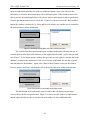
Figure 5-1: Example of a text based menu ......................................................................................... 28
Figure 5-2: Example of a graphic based menu. ................................................................................... 28
Figure 5-3: Concept rendition 1 ......................................................................................................... 30
Figure 5-4: Concept rendition 2 ......................................................................................................... 30
Figure 5-5: Concept rendition 3 ......................................................................................................... 31
Figure 5-6: Front view of the Sony ACX075AKM-7. ............................................................................. 33
Figure 5-7: Front view of the Hantronix HG 3202040. .......................................................................... 33
Figure 5-8: Top side of the OMAP5912 OSK with I/O ports labelled...................................................... 34
Figure 5-9: Backside of the OMAP5912 OSK with I/O ports labelled ..................................................... 35
Figure 5-10: Example layout of a wireless system ............................................................................... 42
Figure 5-11: Airborne WLNG-ET-DP101 ............................................................................................ 45
Figure 5-12: Integrated wireless module options ................................................................................. 45
Figure 6-1: Data Transmission Flow Chart.......................................................................................... 47
Figure 6-2: Complete System Block Diagram...................................................................................... 48
Figure 6-3: Module Integration Diagram ............................................................................................. 48
Figure 6-4: Pull down/up resistor configuration.................................................................................... 50
Figure 6-5: Bounce time for mechanical switches................................................................................ 51
Figure 6-6: User input schematic ....................................................................................................... 52
Figure 6-7: Sample of positive LCD display ........................................................................................ 53
Figure 6-8: Sample negative LCD display image................................................................................. 53
Figure 6-9: Power Circuit Schematic. ................................................................................................. 56
Figure 6-10: Pin Designation for LP324M. .......................................................................................... 57
Figure 6-11: Suggested Voltage Reference Circuit .............................................................................. 57
Figure 6-12: Voltage Reference Circuit............................................................................................... 57
Figure 6-13: Pyramid of Software in Embedded Systems..................................................................... 62
Figure 6-14: Screenshot of FreeStyle Connect Data Management software. ......................................... 64
Figure 6-15: Screenshot of Advanced Serial Port Monitor application.................................................... 65
Figure 6-16: Screenshot of Minicom application. ................................................................................. 67
Figure 6-17: Screenshot of Glad development environment. ................................................................ 68
Figure 6-18: Functionality flowchart for GUI. ....................................................................................... 69
Figure 7-1: Simulation Layout for LCD Driver Circuit............................................................................ 71
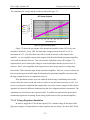
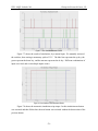
Figure 7-2: Chart of DC Sweep Outputs ............................................................................................. 72
- vii -
WPI – MQP Ireland A’06
Enterprise Research Centre, UL
Figure 7-3: Internal Schematic for LP2966.......................................................................................... 73
Figure 7-4: DC Sweep for LP2966M .................................................................................................. 74
Figure 7-5: Simulation layout for voltage reference.............................................................................. 74
Figure 7-6: User Interface Simulation Layout ...................................................................................... 75
Figure 7-7: User Interface Simulation Results ..................................................................................... 76
Figure 7-8: User Interface Timed Simulation Results ........................................................................... 76
Figure 7-9: User Interface Timed Momentary Simulation Results.......................................................... 77
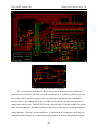
Figure 7-10: ExpressSCH and ExpressPCB linked files indicating connections...................................... 78
Figure 7-11: Trace examples............................................................................................................. 80
Figure 7-12: LCD PCB version two with top and bottom traces as well as solder mask. .......................... 81
Figure 7-13: Topside of LCD driver circuit PCB version two with components........................................ 81
Figure 7-14: Backside of LCD driver circuit PCB version two................................................................ 82
Figure 7-15: User input PCB Design and layout with components......................................................... 82
Figure 7-16: LCD PCB as seen in ExpressPCB .................................................................................. 83
Figure 7-17: User Input PCB as seen in ExpressPCB.......................................................................... 83
Figure 7-18: Voltage regulator ........................................................................................................... 85
Figure 7-19: Full Descriptive Schematic for LP324M ........................................................................... 85
Figure 7-20: LP324M Functionality Test 1 .......................................................................................... 87
Figure 7-21: Severed HiRose Trace................................................................................................... 87
Figure 7-22: Op-amp railing characteristic chart .................................................................................. 88
Figure 7-23: Temporary Solution for LP324M ..................................................................................... 89
Figure 7-24: Update LCD Driver Circuit .............................................................................................. 89
Figure 7-25: Example of bounce on user input pushbuttons ................................................................. 90
Figure 7-26: Graphical User Interface Functionality Diagram................................................................ 92
Figure 7-27: Screenshot of PyGlucoRdr's main window and Get Data window....................................... 93
Figure 7-28: Screenshot of main window and Send Data window. ........................................................ 93
Figure 7-29: Screenshot of main window and Messages window.......................................................... 94
Figure 7-30: Tables in glucoRdrDB. ................................................................................................... 95
Figure 7-31 Selection of table from Hitachi giving LCD terminology ...................................................... 97
Figure 7-32 Selection of table from Hitachi giving LCD terminology ...................................................... 97
Figure A7-1: Etching Machine ......................................................................................................... 147
Figure A7-2: Cutting PCB board to size............................................................................................ 148
Figure A7-3: Photo-resist board diagram .......................................................................................... 149
Figure A7-4: Removing Photo-resist Protective Layer........................................................................ 149
Figure A7-5: Diagram of combining board with mask......................................................................... 149
Figure A7-6: Board insertion to Transparencies ................................................................................ 150
Figure A7-7: UV Exposure machine at the University of Limerick........................................................ 150
Figure A7-8: PCB board placed in Exposure Machine ....................................................................... 150
Figure A7-9: Board with Photo-resist................................................................................................ 151
Figure A7-10: Boards at the end of developer bath............................................................................ 151
Figure A7-11: Drying PCBs after bubble etching ............................................................................... 152
Figure A7-12: Smaller Drill .............................................................................................................. 152
Figure A7-13: Drilling holes on the LCD driver circuit. ........................................................................ 153
Figure A7-14: Drilling holes the user interface PCB. .......................................................................... 153
Figure A7-15: Large Drill................................................................................................................. 153
Figure A7-16: PCB Creation Flow Chart........................................................................................... 154
- viii -
WPI – MQP Ireland A’06
Enterprise Research Centre, UL
List of Tables
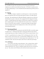
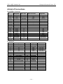
Table 3-1: Recommended Blood Glucose Range for People with Diabetes ........................................... 10
Table 3-2: Comparison chart for glucometer ....................................................................................... 15
Table 5-1: Display options for LCDs................................................................................................... 32
Table 5-2: Comparison of LCD pin connections. ................................................................................. 32
Table 5-3: Comparison of LCD power allotments. ............................................................................... 32
Table 5-4: Comparison of LCD prices. ............................................................................................... 33
Table 5-5: Wireless Chip Options for Embedded Design...................................................................... 44
Table 5-6: Integrated Wireless Systems ............................................................................................. 45
Table 6-1: LCD Viewing Modes ......................................................................................................... 54
Table 6-2: Pin Designation for LCD.................................................................................................... 55
Table 6-3: Results of spying on RS-232 communication. ..................................................................... 66
Table 6-4: Command to trigger FreeStyle Mini memory dump. ............................................................. 66
Table 7-1: Predicted values for the LP324M ....................................................................................... 71
Table 7-2: Measured Resistance and Expected Values ....................................................................... 86
Table 7-3: Actual and Expected Pin Values for LP324M ...................................................................... 86
Table 7-4: Op-amp railing characteristic ............................................................................................. 88
- ix -
WPI – MQP Ireland A’06
Enterprise Research Centre, UL
Executive Summary
Throughout the developed world, the spread of diabetes in the general populace is on the
rise. According to the World Health Organization (WHO), over 171 million people were
afflicted with Diabetes mellitus (i.e. hyperglycaemia or “elevated blood glucose levels”) in the
year 2000. King et al predict a 42% and 170% increase in patients diagnosed with the disease in
developed and developing countries, respectively, within the next twenty years in their 1998
article, “Global Burden of Diabetes, 1995-2025.” Such an increase in diabetic patients demands
technological advances to better facilitate the management, research, and analysis of diabetes in
the near future.
Ireland, with a population of just over four million, currently harbours over 200,000
diabetics. The Diabetes Federation of Ireland predicts that as many as 200,000 additional Irish
are unaware of their affliction with diabetes (“Ireland loosing in EU diabetes battle”). The
federation also claims that the number of people with diabetes in Ireland is to double by the year
2010, fuelled mainly by poor diet and the onset of sedentary lifestyles. With 10% of the total
healthcare budget of Ireland—over €350.5 million—dedicated to managing expensive and
preventable complications of diabetes (€210.3 million), emergency medical response and
ambulatory care (€87.6 million) for diabetic patients, and towards effective management of the
disease (€56 million), the need for the collection of accurate and reliable diabetic data (such as
blood glucose level readings) for statistical research and analysis geared towards reducing the
cost of quality healthcare for diabetics and focused upon improving the quality of life and life
expectancy of those afflicted with the disease is realized (Clarke, 2002).
General practitioners advise diabetics to regularly test and record their blood glucose
levels. Patients afflicted with Type I diabetes often need to adjust their blood glucose levels with
insulin injections. The review of these recorded logs by general practitioners occupies time that
could be better focused on providing healthcare to other patients. A device capable of collecting
and organizing data from existing and soon-to-be-developed glucose meters and storing this data
in a centralized database would allow for this reprioritization of general practitioner care without
placing the care of their diabetic patients in jeopardy. The ability for near real time
communication between patient and general practitioner could even reduce the number of checkups required because feedback is provided more frequently to the patient by the general
practitioner or healthcare professional. By storing diabetic data in a centralized database, the
-1-
WPI – MQP Ireland A’06
Enterprise Research Centre, UL
foundation for the statistical research and analysis of diabetes from a vantage point previously
unavailable is laid.
The Enterprise Research Centre (ERC) at the University of Limerick (UL), Ireland is
interested in the creation of this personal health monitor interface. In 2005, a student research
team from Worcester Polytechnic Institute (WPI), USA helped the ERC implement a proof-ofconcept device that could interface with an existing glucometer, the TheraSense FreeStyle Mini.
Our research builds upon the initial findings of 2005 team and aims to deliver an improved
prototype, a device comprising of a short-range wireless transmitter capable of interfacing with
existing glucometers, retrieving any data stored, and updating individual patient data on a remote
database. Our efforts were to focus on generating useful documentation to accompany our
product to enable future research teams to quickly pick-up development.
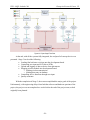
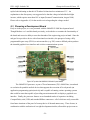
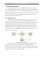
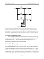
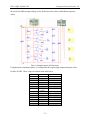
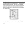
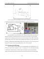
At the core of our proof-of-concept design is the OMAP5912 OSK development board,
as recommended by the 2005 student research team. The figure below illustrates how the
board’s capability to interface with numerous external devices through different means
contributes to our development platform.
System Level Diagram
-2-
WPI – MQP Ireland A’06
Enterprise Research Centre, UL
Our device’s hardware is comprised of four main subsections: a user input circuit, an
LCD driver circuit, a wireless module, and the OMAP5912 OSK development board. Each
subsystem is integral to the functionality of the product and was designed for the average
diabetic. The user input is limited to three selection buttons, which control a text-based
graphical user interface (GUI). We designed the LCD module to have a high level of clarity
while maintaining a small size. Wireless capability is enabled though the fully integrated
Airborne ABEB-10BT Wireless Ethernet Bridge. All of the software that controls this device is
located on the development board, which is powered by the open source Linux operating system.
In the end, we were able to provide the Engineering Research Centre with all of the
subsystems to create a working proof-of-concept device capable of interfacing with a glucose
meter. Our proof of concept included a functional graphical user interface and the ability to
successfully pull data from the glucose meter. Unfortunately, due to unforeseen difficulties with
enabling LCD support in the operating system, final compatibility testing with our LCD was
delayed. When the unit was finally connected to the system, it became apparent that the LCD
itself may not be functioning within normal parameters. We were, however, able to confirm that
all software was operational by making slight adjustments to use the 2005 student research
team’s LCD unit. Moreover, all of the documentation to recreate our development computer and
recreate our proof-of-concept design has been generated and left with ERC for future
development. Our research team is hopeful that research continues on this device and comes to
market one day in the near future to aid the study of diabetes and, more importantly, those
afflicted with the disease.
-3-
WPI – MQP Ireland A’06
Enterprise Research Centre, UL
1 Introduction
Throughout the developed world, the spread of diabetes in the general populace is on the
rise. According to the World Health Organization (WHO), over 171 million individuals were
afflicted with Diabetes mellitus (i.e. hyperglycaemia, elevated blood glucose levels) in the year
2000. In their 1998 article “Global Burden of Diabetes, 1995-2025,” King et al. use diabetes
research to estimate the impact of the disease on men and women in the developing world
(Aubert). They predict an increase of 42% and 170% in patients afflicted with diabetes in
developed and developing countries, respectively, within the next 20 years. Such an increase in
diabetic patients motivates technological advances in order to facilitate the future management,
research, and analysis of this disease.
The Republic of Ireland is feeling the growing affect of diabetes on its citizens. A WHO
census in 2000 reported an approximate 86 thousand Irish citizens afflicted with the disease. In
2006, the Diabetes Federation of Ireland estimated that at least 200 thousand known diabetics
resided in Ireland, with approximately 200 thousand additional persons unaware that they are
afflicted with the disease. In addition, there could another 250 thousand more people in Ireland
considered “pre-diabetic”—that is, people who will require insulin injections if lifestyle changes
are not made over the course of the next five years. With a population of just over 4 million and
17% of the population in danger of enduring a lifetime of diabetes, the collection of data from
Irish diabetic patients for research and analysis could aid in determining the most efficient manor
in which to deal with the disease.
Diabetic patients are advised to test their blood glucose levels periodically and in some
cases use injections of insulin to maintain healthy levels of glucose in their blood. Doctors
recommend that patients keep a record of blood glucose levels for review at routine
examinations. The review of handwritten logbooks is time consuming for both the patient and
the doctor. With the creation of a device capable of data collection and organization, and that is
compatible with present and future types of glucometers, the review of data logs will be easier
not only for the doctor, but for the patient as well. This device could provide physicians with a
means of real time communication to pass along advice to the patient for controlling their blood
glucose level. Furthermore, the device will lay the foundation both for statistical research and
for analysis of diabetic patients and allow for remote monitoring of a patient’s status by
healthcare providers.
-4-
WPI – MQP Ireland A’06
Enterprise Research Centre, UL
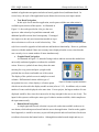
Few products are available for recording and graphically displaying blood glucose data
digitally or sending data to remote locations. Some glucometers like the Freestyle Mini (Abbot
Laboratories Ltd) can store past readings and upload data onto PCs so the user is not required to
enter data manually. The GlucoMON from Diabetech, LP, is the only device found that
interfaces with a glucometer and sends the information to a remote location. In 2005, a team of
student researchers from Worcester Polytechnic Institute (WPI) in conjunction with the
Enterprise Research Centre at the University of Limerick made significant progress towards
implementation of a proof-of-concept device capable of interfacing with standard, off-the-shelf
glucometers and synchronizing the stored data with an external database via a wireless network.
However, none of these programs or devices is yet capable of collecting reliable data for
statistical analysis. The 2005 student research team was not able to complete the proof-ofconcept device due to technical limitations of their wireless implementation and developed
firmware. A few research companies are currently trying to develop devices capable of
gathering data and transmitting it wirelessly to a central location, but currently no products are
available for this type of action.
The goal of this project is to create a proof-of-concept device able to transmit data
synchronised from a glucometer wirelessly to a remote database. Our project addresses the
problem of collecting reliable data from diabetic patients for statistical analysis, while making an
improvement to the lifestyle of said diabetic patient. This proof-of-concept product will be
capable of gathering, transmitting, and organizing blood glucose data in a central remote location
with little need of technical experience on the part of the user. The success of this proof-ofconcept would not only provide the data necessary to formulate an argument for the need for real
time data evaluation of all forms of health monitors, but also affirm the usefulness of wireless
medical telemetry in both the Irish and world markets.
-5-
WPI – MQP Ireland A’06
Enterprise Research Centre, UL
2 Project Description
The purpose of this chapter is to present the reader with the objectives of the project as
well as the initial product specifications. This should aid the reader in understanding the
direction of our project.
2.1 Project Objective
The following is an excerpt from the project description provided by John
Harris and Dr. Mark Southern of Enterprise Research Centre (ERC) University of Limerick
(UL); Appendix A1 contains the original text.
“The aim of the project is to develop and apply a wireless data transmission technology
for real-time data acquisition of remote patient data in a primary care environment. Possible
applications include the monitoring of diabetes, cardiovascular, asthma and chronic disease
management.
The objective is to deliver a prototype wireless interface device comprising of a shortrange wireless transmitter communicating over a proprietary wireless access point (WAP)
updating individual patient data in a remote database over the internet. The target output is a
microprocessor-based mobile RF transceiver interface” (Harris 2005).
2.2 Project Mission
Taking the above project objective, we established a project mission. Our project aims to
assist the Engineering Research Centre at the University of Limerick design, develop, and
implement a proof-of-concept wireless system capable of remote data monitoring and the realtime acquisition of remote patient data in a primary care environment with intent for future
statistical research and analysis on said data. We will fulfil our mission by:
1. Developing a device and its firmware with prior, current and soon to be developed
glucometer for data retrieval,
2. Making our device portable and use existing infrastructure (i.e. wireless) to report
readings to a database system for future analysis,
3. Constructing an externally-hosted, standards-based database system for use by general
practitioners and capable of supporting multiple patients while adhering to privacy
concerns,
-6-
WPI – MQP Ireland A’06
Enterprise Research Centre, UL
4. Designing and implementing an intuitive user interface for easy accessibility to our
device’s controls.
2.3 Project Specifications
Doing more research into the issues this project deals with, and through discussions with
our project advisors and liaisons, we made the following determinations:
•
Proof-of-concept device
o The end goal should not be to have a finalized marketable product. Miniaturization
and fine-tuning can happen at another time.
Functionality of the major subsystems is the most important aspect of this
project.
o Fit inside a metal case 45cm x 33cm x 15cm with a laptop computer.
o Complete documentation on how to recreate results.
o Use little to no proprietary software or hardware in the development of the device.
•
User Interface
o Large display
o Clear user commands
o Simple graphic user interface (GUI)
•
Microprocessor
o
o
o
o
•
Database
o
o
o
o
•
Ability to interface with glucometers for data transfers
Feedback on operations
Built-in memory for temporary data storage
Built-in clock
Secure location
Unique personal identification numbers
Easily accessible data for the user and doctor
Logical data organization
Wireless Characteristics
o Secure data transmission
o High encryption level
o Low cost – specific figures are not available as to cost, since this is a proof-ofconcept device
o Indoor and outdoor use
-7-
WPI – MQP Ireland A’06
Enterprise Research Centre, UL
3 Background
In this chapter, we present a brief overview of diabetes and its impact on the world
population. We then describe some of the devices used to keep control diabetes, and how
medical telemetry is a key element of simplifying the life of diabetic patients. Finally, we
explain how prior products and research in this field relate to our project.
3.1 Diabetes mellitus
Diabetes mellitus is a chronic disease that can be inherited (i.e. Type I Diabetes) or
acquired later in life (i.e. Type II Diabetes, a.k.a. late-onset diabetes). The disease causes a
deficiency in or impotency of insulin produced by the pancreas. Such a deficiency results in
increased concentrations of glucose in the blood. This, in turn, can damage many of the body's
systems, particularly the blood vessels and nerves composing much of the circulatory system
(“Diabetes Overview”). Diabetes is on the brink of becoming a worldwide epidemic, with over
one hundred million people estimated to be afflicted the disease. The fact that much of the
diabetic population is unaware of their condition is also of great concern.
Figure 3-1: The Prevalence of Diabetes
(“Diabetes: Facts & Figures”)
-8-
WPI – MQP Ireland A’06
Enterprise Research Centre, UL
As illustrated in Figure 3-1, diabetes is a condition that affects every nation. Diabetes
mellitus occurs throughout the world, but is more common (especially Type II) in developed
countries. The prevalence of diabetes is increasing the fastest in Asia and Africa, where the
highest concentration of patients will likely be found by 2030 (“Diabetes: Facts & Figures”).
The two main forms of diabetes are Type I and Type II. In Type I, the pancreas is unable
to produce an adequate amount of insulin, and thus a person who has Type I diabetes must take
insulin daily to live. Figure 3-2 illustrates and describes some of the mechanisms at work in the
body of a diabetic. The symptoms of Type I diabetes usually present over a short period,
although the destruction of the beta cells could have begun before any symptoms are ever
noticed. Main symptoms include increased thirst and urination, constant hunger, weight loss,
blurred vision, and extreme fatigue (“Diabetes Overview”).
Figure 3-2: Causes of Type I Diabetes
(“Diabetes Overview”)
Type II diabetes is the more common form of the disease. In Type II, or late onset
diabetes, the pancreas produces the correct amount of insulin; however, the body of the person
cannot effectively use the insulin. Symptoms of Type II diabetes develop gradually over the
course of the patient’s life. The symptoms may include fatigue or nausea, frequent urination,
unusual thirst, weight loss, blurred vision, frequent infections, and slow healing of wounds or
sores (“Diabetes Overview”). Once this condition is recognized patients keep track of their
blood glucose levels with a device called a glucometer.
-9-
WPI – MQP Ireland A’06
Enterprise Research Centre, UL
3.1.1 Glucose Monitoring
To regulate blood glucose levels naturally, doctors recommend that people maintain a
healthy lifestyle that includes regular exercise and a lean, well-balanced diet. In addition,
diabetics need to check their blood glucose levels with the aid of testing device, such as a
Time of Test
Goal Plasma Glucose
Before meals
90-130 mg/dL (milligrams per decilitre)
Before bedtime snack (1-2 hours after a
meal/postprandial)
less than 180mg/dL
Every three months
less than 7%
Table 3-1: Recommended Blood Glucose Range for People with Diabetes
(“All About Diabetes”)
glucometer. The frequency of blood glucose level checking varies between patients as it largely
depends on the severity of their condition.
The monitoring of blood glucose levels at home can occur either through a invasive or
non-invasive procedure. The most common method of testing blood glucose levels involves
pricking a specified part of the body with a small needle, in order to draw a small amount of
blood. The drop of blood is then collected on a test strip and inserted into a glucose meter. The
glucose meter analyses and then numerically displays the glucose concentration level in the
blood sample. Section 3.3.1 goes more in depth on the different types of glucometers on the
market, from older versions to the newer versions that implement the principles of medical
telemetry.
3.2 Medical Telemetry
In its simplest form, medical telemetry (or “telehealth,” for short) involves delivering
medicine or medical information to people from a distance (“Defining Telemedicine, Telehealth,
and the Consumer”). This allows the patient to stay at home, but still be able to communicate
with medical staff. Telemedicine is a subset of telehealth, which involves the implementation of
information technology and of communication principles (“Defining Telemedicine, Telehealth,
and the Consumer”). The research done on telemedicine includes two main parts: one deals with
wireless health monitors and the other with glucometers themselves (Section 3.2.1). With this
project focused on wireless collection of data from glucose monitoring instruments, we analyzed
the different techniques and technologies already available for wireless collection of information
for other types of health monitors.
- 10 -
WPI – MQP Ireland A’06
Enterprise Research Centre, UL
3.2.1 Wireless Health Monitoring
Several medical institutions have begun implementing modern day technology into
medical data logging - including web portals, electronic medical records, and virtual private
networks (VPNs). This modern day technology improves the speed, quality, safety, and cost
profile of healthcare. Figure 3-3 is an example of how wireless monitoring can work in a
medical institution.
Figure 3-3: Wireless data collection
(“Defining Telemedicine, Telehealth, and the Consumer”)
Patients use certain sensors that transfer their data to a server where the practitioner can
read and monitor their condition. This technology is an adaptation of wired technologies on
traditional personal computers (PCs), which require users to work from a computer physically
connected to a local network. The recently developed wireless capture of patient data reduces
the need for nursing staff to sit at computers and enter basic data. Such digital solutions offer
dramatic improvements over the days of paper files, chart-chasing, lengthy delays, and illegible
entries. Wireless deployments have made significant improvements to the quality of healthcare,
a positive impact felt both inside and outside the organization.
Increased intelligence and the lowered power consumption of the new generation of
microcontrollers and digital signal processors (DSPs) make a complete new range of intelligent
monitor applications possible. Further need for privacy protection and acceptance of implantable
- 11 -
WPI – MQP Ireland A’06
Enterprise Research Centre, UL
sensors and devices require the introduction of a wireless personal network. Different
applications of wireless personal area networks in telemedical environments include:
Intelligent portable health monitors, such as:
o ECG and
o epilepsy monitoring,
Intelligent control of medication delivery using:
o wireless sensing,
o dosing, and
o compliance monitoring
Breathing monitors for:
o sleeping disorders,
o stress monitoring,
o biofeedback techniques, and
o circadian rhythm analysis
Activity monitoring using accelerometer
Aids for disabled individuals.
Computer assisted rehabilitation.
Battlefield soldier monitoring.
These technologies could become an unseen part of patients’ daily lives. Theoretically, a
patient could simply wear and/or use a sensor with a wireless communication link that enables it
to receive instructions and transmit data (usually time stamped) to a remote database (“Defining
Telemedicine, Telehealth, and the Consumer”). The patient could also wear and/or use an
automatic medication-dosing device with a wireless link that transmits the dosing history (dose
amount and time) to a remote database.
For diabetics a remote intelligent control system could determine when a new blood
glucose measurement is necessary, and use the wireless link to signal the sensor, either
automatically make the measurement or request the patient make the measurement manually.
Then, the data could be transmitted wirelessly to a remote database where an algorithm could
recalculate the dosage level and administration timing. This new dosage schedule once received
by the dosing device/recorder is either automatically administered, or the patient uses the dosing
device/recorder to administer the dosage manually. The development of built in contingencies
would need to coincide with the development of these technologies. For example, if the
communication link were not available to deliver the new dosage schedule, the system would
need to recalculate a new dosage schedule on its own and try to transmit again. A key part of
this system would be the supervisory medical personnel who could access the database on a
regular basis to monitor the patient measurements and dosing levels. A supervisory algorithm
- 12 -
WPI – MQP Ireland A’06
Enterprise Research Centre, UL
would also be necessary to monitor operation of the system and alert medical personnel as
needed (“Defining Telemedicine, Telehealth, and the Consumer”).
Several new rehabilitation therapies could make use of such devices used by the patient
in their home environment during routine activity. Using wireless communication technologies
to monitor the patient and assess the effectiveness of therapy does not hinder the patient in any
way. This also allows the doctors and rehabilitators to adjust the patient’s regimen if necessary
without having the person leave home. All of these ideas are purely hypothetical and not yet
available to consumers, but are along the lines of what this project aims to make possible.
3.3 Prior Art and Research
In this section, we investigate products currently available to diabetics for control of their
disease, as well as some technology with attributes previously described in section 3.3. This
information indicates which customer needs are currently being filled and to what portions of the
market have been saturated. Exploring and comparing these products is advantageous because of
the different elements each employs. Since our project involves wireless communication and
wireless transmission of data, we researched different methods of communication as well as the
different elements that go into wireless communication. In 2005, a student research project from
WPI worked on a very similar project and learned many lessons that will be helpful in the
completion of this project.
3.3.1 Prior Art for Glucometers
A glucometer, as previously mentioned, is device used by diabetics to measure blood
glucose levels. The main principles a glucometer as described on WebMD are:
1. A chemical is presented on the test strip, which on contact with glucose, produces a colour.
The meter measures this colour intensity and the level of glucose present is expressed in
mg/dl.
2. The other type of glucometer measures the electric current in the blood, which depends on
the amount of glucose present. When blood is put on the test strip, an enzyme transfers
electrons from glucose to a chemical in the test strip and the meter measures the flow of the
electrons as current. The amount of current depends on the amount of glucose present and
the meter produces the reading in mg/dl.
(“Diabetes Overview”)
Glucometers, vary in features, readability (some having larger displays or even spoken
instructions for the visually impaired), portability, speed, size, and even cost. Current devices
provide results in less than 15 seconds and can store the information obtained for future use.
- 13 -
WPI – MQP Ireland A’06
Enterprise Research Centre, UL
These glucometers can also calculate an average blood glucose level over a period. Some meters
also feature software kits that retrieve information from the meter and display graphs and charts
of past test results (“Diabetic Meter Strips”). This software is either included in the package by
the manufacturer or can be bought as an additional accessory at anytime.
Using a glucose monitor regularly has many advantages for a person living with diabetes.
A glucometer enables diabetics to take care of themselves without visiting doctors and labs for
tests. Instead, they can monitor their own blood glucose levels. It also promotes the well-being
of the patient by allowing him/her to control the situation. Glucometers also provide a better
understanding of medications taken by patients and help them alter dosages as necessary. Each
glucometer has its own specialized type of test strip that only works with that type of glucometer
and no other. The test strip has a code, and before any test trip can be used, the glucometer must
be set to the correct code. We hope to interface our device with standard types of glucometers
and provide a wireless link to send recorded data to a central database. Ideally, the product will
one day be able to integrate with all types of glucometers. However, we will attempt to integrate
the Free Style Mini or the One Touch Ultra to our proof-of-concept device.
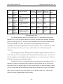
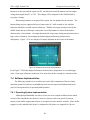
Figure 3-4: FreeStyle Mini Glucometer
The Free Style Mini and the One Touch Ultra are both common types of glucose meters that the
ERC had obtained for a past research project, and so were readily available for our team. Figure
3-4 above and Figure 3-5 below show the glucometers.
Figure 3-5: OneTouch Ultra Glucometer
- 14 -
WPI – MQP Ireland A’06
Enterprise Research Centre, UL
Understanding and examining currently available glucometers will help us understand what
elements of the device are important to the user. We are also interested in how the devices
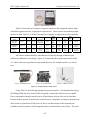
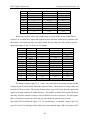
interface with personal computers for digital storage of glucose information. Table 3-2 shows
the different types of glucometers that are available on the market.
FreeStyle
Mini
One Touch
Basic
One Touch
Profile
Accu-Check
Advantage
Accu-Check
Complete
One Touch Ultra
Manufacturer
TheraSense
LifeScan
LifeScan
Roche/
Boehringer
Roche/
Boerhinger
LifeScan
Sample (min)
0.3uL
10uL
10uL
4uL
4uL
1.5uL
Lot
Calibration
Button
Button
Button
Chip
Chip
Button
Memory
250 tests with time
& date, 14d avg.
75 Tests with
Time and Date
250 tests with
time & date. 14
/30d averages 15
event codes
100 with time and
date
1000 with time &
date multiple data
management
functions
150 tests with
time and date and
14/30 day average
Download
cap.
Yes
Yes
Yes
yes
yes
Yes
Test Time
15 sec
45 sec
45 sec
up to 40 sec
up to 40 sec
5 Seconds
Battery
Two AAAA
Alkaline
Two AAA
alkaline
Two AAA
alkaline
Two AAA
Alkaline
Two AAA
Alkaline
3Volt Lithium Ion
Tests/Battery
~1000 tests
~1000 tests
~1000 tests
~700 tests
~1000 tests
~1000 tests
Auto Shut Off
2 minutes
5 minutes
5 minutes
5 minutes
3 minutes
2 minutes
Price Range
$$$
$$
$$$$
$$
$$$$
$
Size (in)/Wt.
2x3.8x1 2.1 oz
4.3x2.6x1.2
4.5oz
4.3x2.6x1.2 4.5
oz
3.6x2.3x0.6 3 oz
4.8x2.8x1.1 4.4 oz
3.1 x 2.25 x.85
1.5 oz
Comments
Very small sample
size. Samples from
arm. ***Coulometric measurement
New larger
display screen.
Display can be
set in 17
languages
Display can be
set in 19
languages. Voice
synthesizer
available
May add blood
during first 15
seconds. Voice
synthesizer
available
4 languages Blood
may be added to
strip during first
15 seconds
Can touch test
strip sample area
without affecting
results, alternative
site testing
Table 3-2: Comparison chart for glucometer
(“Diabetic Meter Strips”)
Many diabetics find taking measurements painful and annoying because they must
puncture their skin for a reading. This has inspired the development of alternative forms of
continuous glucose monitoring systems. The MiniMed Continuous Glucose Monitoring System
is a device consisting of a catheter inserted just below the surface of the skin. The catheter
collects small amounts of fluid and then measures the glucose level in the blood over a 72-hour
period (for more information see MiniMed.com). In 2001, the FDA approved the GlucoWatch, a
watch-like device that helps people with diabetes measure their blood glucose via tiny electric
currents. It draws small amounts of fluid from the skin and measures blood glucose levels three
times per hour for up to 12 hours (for more information see GlucoWatch.com).
- 15 -
WPI – MQP Ireland A’06
Enterprise Research Centre, UL
3.3.2 Prior Art for Wireless Transmission of Glucometer Data
Currently there are relatively few methods of transferring data from a glucometer to a
storage device over a wireless network. Secure data logging capabilities for glucometers are
exclusively though USB or RS232 to connect to a PC. One Windows Mobile based software
program allows users to manually input glucose readings.
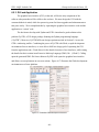
Figure 3-6: Microsoft Windows mobile glucose data logging interface
(“Glucose Tracker”).
This $20 software application developed by Handango is for a Windows enabled cell phone or
PDA (“Glucose Tracker”). It is possible to upload the recorded information onto a PC, but there
is no further functionality for sharing this information with a doctor. Since the information input
manually, the risk of incorrect or fabricated data exists. In addition, the upload of the
information onto a PC is a manual and sometimes complicated process requiring the user to have
a good deal of technical knowledge, as well as spending extra time to upload the information.
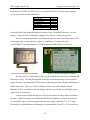
A transmitting glucose monitoring system developed for parents to monitor their
children’s glucose readings is the GlucoMON. This package offered by Diabetech is a
specialized glucometer and wireless technology package which requires very little thought on the
user’s part (“GlucoMON”). When the glucometer is placed in the package after taking a glucose
reading, it automatically retrieves the data and sends it to a location predetermined by the user or
administrator of the unit. It is possible to set the device to send the information to multiple cell
phones or email addresses. A monthly charge is associated with this device similar to any type
of two way paging service.
- 16 -
WPI – MQP Ireland A’06
Enterprise Research Centre, UL
Figure 3-7: GlucoMON package for the wireless transmission of glucose
(“GlucoMON”)
This device is currently in the test stage and costs $400 to become involved with the research
program not including the LifeScan® glucometer, lancer, or test strips. Diabetech offers some
other products that are two-way pagers for the transfer of glucose information; however, none of
these alternatives interface directly with a glucometer.
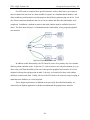
A Finnish company called eHIT, is proposing a concept product that is advertised to use
existing products with Bluetooth, WLAN, or infrared capabilities to tie together a network of
health monitoring systems (“Solutions”). eHit’s proposal is to develop all of the software
necessary for interfacing the products, however they are not interested in being part of the
development of such products.
Figure 3-8: eHIT product concept diagram
(“eHIT”)
The concept shown in Figure 3-8 connects all of the same concepts as we are aiming for
in this project. However, each of the category descriptions are quite vague, with the use of a
“personal wellbeing monitoring device” and a “smart phone PDA” and the “Wellbeing Portal”
- 17 -
WPI – MQP Ireland A’06
Enterprise Research Centre, UL
all of these elements will be integrated. The idea is to use all different types of existing wireless
technology to transmit the information, and then have data storage for all of the information.
These products are the technologies available on the market for glucose data record
keeping, as opposed to keeping hand written logs of the information. The Handango cell phone
software does not transmit, but allows the user to carry a digital log of glucose readings. The
main purpose behind GlucoMON is for families to keep track of their loved ones. There is no
database service or glucose tracking software to go along with GlucoMon as of yet. The eHIT
solution looks to be the product with the most similar mission to this project. However, by using
only wireless enabled technology the product is restricted to people who have the means to
purchase such products then configure them with the eHIT software.
3.3.3 Prior Student Research
In 2005, the Enterprise Research Centre (ERC) at the University of Limerick sponsored a
student research project to develop a wireless system capable of gathering data from many
different health information systems and transmitting the data wirelessly to a remote database.
The system was also to include the capability to receive information and display messages back
to the user regarding the analysis of the information gathered. The 2005 student team completed
the project with basic functionality of the product only. They recommended a follow up project
due to the potential of the product.
The 2005 student team obtained a development board in order to eliminate the need to
design an entire system from discrete components. They selected the TMD OMAP5912 OSK
development board for its processing abilities and versatility of expansion ports. Our research
project will use the OMAP board on the recommendation of the 2005 student team although it
has more processing and memory storage power than necessary for this project. After the proofof-concept is complete, the process of miniaturization can begin by eliminating the unnecessary
functionality.
One of the most important recommendations made by the 2005 student team was to be
aware of lead-time on parts. Due to some long delays and time constraints nearing the end of the
project, the 2005 team was forced to implement a proprietary wireless technology into their
design. Two problems arose from this solution. First, proprietary technology is not desirable in
a proof-of-concept design because the technology cannot be used in the final product without
causing a great impact on the cost of production. The second problem arose from the
- 18 -
WPI – MQP Ireland A’06
Enterprise Research Centre, UL
OMAP5912 OSK development board. The wireless capable USB dongle drew so much power
that the board would crash after only a few seconds of operation, and the distances for successful
transmissions was very short. We discovered that the USB port, which is integrated into the
OMAP5912 OSK development board, has non-standard wiring and cannot support any type of
WLAN technology due to the power requirements of such devices (“OSK”). Another challenge
that the 2005 team encountered because of long lead times on products was with their specially
designed PCB. Because the board was manufactured at UL, the pitch of the components used is
limited. UL has limited technology for PCB production, which caused a problem with the ribbon
cable header for the LCD selected by the team. The trouble creating the LCD driver circuit
compromised the capabilities of the LCD in the end. These lessons and recommendations were
taken into account as the development of this product was restarted.
The progress of the 2005 student research team at the University of Limerick illuminated
many issues present in the wireless health monitor project. The concepts that were formulated
were helpful in gaining a starting point; however, all the information was re-investigated and
confirmed. By doing this, a much more fully developed product was produced for the Enterprise
Research Centre at the University of Limerick.
- 19 -
WPI – MQP Ireland A’06
Enterprise Research Centre, UL
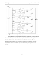
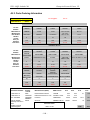
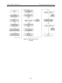
4 Project Planning
In order to approach this project in a systematic manner a step-by-step plan of action was
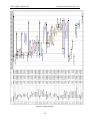
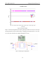
developed early in the effort. The top level Gantt chart shown in Figure 4-1 allowed for
advanced consideration of tasks in relation to both the compilation of this report and the
completion of the project.
- 20 -
WPI – MQP Ireland A’06
Enterprise Research Centre, UL
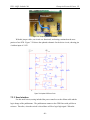
Figure 4-1: Top-level Gantt chart.
- 21 -
WPI – MQP Ireland A’06
Enterprise Research Centre, UL
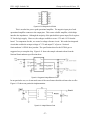
The project was divided into three main phase: research and design, implementation and
testing, and integration of all the subsystems. The hardware and software components of the
project were divided in the flow charts and Gantt chart in order to illustrate that parallel
development took place. Integration of the systems is implicit and occurs later in one of the
aforementioned stages.
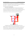
Stage 1 of the project is the research and design portion that lay the foundation of the
project by defining the functionality of each subsystem. This is the stage where the majority of
the planning and design occurred.
Figure 4-2: Project Stage 1 Flow Chart
Top-level diagrams and descriptions for the subsystems were created in this stage. By
the end of this stage, we had a good general understand of not only the project but also the
hardware and the software elements that were in the project. Based on the illustration above,
Stage 1 included the following key tasks:
Background research completion
o Prior art
o Customer needs
Designing
o LCD module
o User interface
o Wireless module
o Development board operating system
o Custom software applications
Parts selection
o LCD and driver
o User interface
o Wireless module
Establishing of the file system on the board
- 22 -
WPI – MQP Ireland A’06
Enterprise Research Centre, UL
Stage 2 of the project covered the individual implementation the major subsystems.
Once realized, each subsystem was tested for expected values and results individually before
being connected to any other part of the system. Stage 2 took the designs, plans, and ground
work from Stage 1 and put them into action.
Figure 4-3: Project Stage 2 Flow Chart
As Figure 4-3 shows, Stage 2 built upon Stage 1. The actual pieces of the subsystems
were built and tested. By the end of this stage, all of the major subsystems had been constructed.
This stage included the following key tasks:
Hardware manufacturing
o Driver for LCD
o User interface
Hardware testing
o Compare to simulations from design
Operating system compiled and loaded onto the development board
Glucometer protocol developed and functional
Graphical user interface functional
Stage 3 of the project covered the integration of the subsystems, assuring positive
connections, and testing the overall system. Taking each of the subsystems, which were
designed to work together, and integrating them into one working product was the goal of stage
3.
- 23 -
WPI – MQP Ireland A’06
Enterprise Research Centre, UL
Figure 4-4: Project Stage 3 Flow Chart
At the end, with all the systems fully integrated, the end proof-of-concept device was
presented. Stage 3 involved the following:
Loading final software revisions onto the development board
Connecting user input and LCD driver PCBs
Upload and logging of data on device from glucometer
Plugging wireless module into development board
o Making wireless transmission
o Making data entry in database
Controlling device functions through user input
Quality assurance
With the completion of Stage 3, the team accomplished the major goals of the project.
Unfortunately, with engineering delays from both the software and hardware portions of the
project, the project was not completed two weeks before the end of the project term, as had
originally been planned.
- 24 -
WPI – MQP Ireland A’06
Enterprise Research Centre, UL
5 Design Methodology
This section discusses the methods we used to design the proof-of-concept product. To
complete this process the product is broken up into several different subsystems. For each of the
subsystems we determine its requirements in relation to the needs of the user and our prior
research. After the system requirements have been established, the subsystem is fleshed out
along with some detail on how it will interface with the rest of the device.
5.1 User Interface Requirements
A user interface includes all the systems the user interacts with, and which affect how the
user experiences the product. The range of customers targeted for this product includes all
diabetic patients and it must be accessible for a range of people who have different technical
expertise, economic standing, and life style. Designing with this large range of customers in
mind, and hoping to make the product easily accessible to as many users as possible, we tried to
keep the end cost low, the need for technical experience limited, and the ease of use very high.
Clarity was the primary concern; we wanted to make the system self explanatory and simple to
use for any level user.
5.1.1 Customer Needs
The needs of the customer should dictate how a product is developed and eventually how
it comes to life. No product can be successful without a market; therefore, the customer is the
most important element in the development process. Through research into the life of diabetic
patients, we were able to establish the current issues diabetics experience in their everyday lives.
The discussion of products currently on the market in Chapter 3 helped identify elements, which
the users found pleasing, as well as the displeasing factors associated with the product. In
Chapter 8, we will make suggestions for features we were not able to incorporate in the proof-ofconcept, but envisioned as integral to the eventual success of the product. The division of this
project’s functional goals into two different groups allows for the distinction between what this
project aims to complete, and the elements identified as important and should be developed later
for a marketable product. The two lists are separated with elements which will be designed and
implemented in the first generation proof-of-concept product presented first, and the
requirements for a marketable product presented second.
- 25 -
WPI – MQP Ireland A’06
Enterprise Research Centre, UL
Proof-of-concept Device Features
•
Clear display - Diabetes can cause a decline in vision, so to accommodate both patients who
are elderly and or have poor vision a clear display capable of large text and images will allow
them to experience comfortably the capabilities of this product.
•
Simple to navigate - The menu system must be very clear and easy to navigate without
much familiarization; something that people feel like they understand immediately when they
start using it.
•
Ability to receive health related messages - The ability for doctors or health services to
send feedback messages to the user is a main feature of this device. The person must be able
to receive information from the internet as well as send and store information there.
•
Clear feedback about operation - Messages such as “Transmitting Now” or “Uploading
Data” will allow to user to see easily that the device is busy and not yet ready for additional
inputs. These informational queues to the user allow them to know what the processor is
thinking and relate to the transfer of information.
•
Secure transmission of information – Health information must be protected by the highest
level of security possible, so the highest levels of wireless security must be implemented. In
addition, the database on the internet must be a secure database only accessible to those who
should have access to the information.
Final Product Features
•
Portable with small form factor – The device needs to be battery powered and its overall
size should not exceed the size of a Personal Digital Assistant (PDA) and should easily fit
into a coat or pants pocket without causing discomfort.
•
Unobtrusive exterior design – The intention of this device is to make life easier for
diabetics and help them blend in with the rest of society. Designing the exterior of the
product to be similar in size and format to a PDA or MP3 player would achieve this goal.
•
Long battery life - One of the main elements of this product is simplifying the lifestyle of
diabetics; therefore, a long battery life is included to reduce the need to worry about whether
the device will keep working or not. A “long” battery life for this type of device would be
between 3-6 hours of continuous operation, because when used normally it will be turned on
- 26 -
WPI – MQP Ireland A’06
Enterprise Research Centre, UL
for short periods of time, then it is switched off, making the device usable for multiple days
without the need for recharging.
•
Easily accessible information - The information gathered and stored by the device should
be easily accessible over the internet by the user, and the doctor.
5.1.2 Display Module
The display, as the face of this product, will be the element the user interacts with the
most. Our main considerations for the display are size, colour capability, brightness, and touch
sensitivity. These characteristics are elements that greatly affect the user as well as limit the
possibilities from a design standpoint. Though small size is an element recommended for the
final product, we would like to incorporate as many of the final features into the proof-ofconcept as possible without causing delays or influencing the final functionality. A small screen
is one element that can be incorporated into the proof-of-concept to show that despite small
screen size the text can still be clear. A screen with a diagonal dimension between 2.5” and 3.0”
should be adequate to achieve this. The ability for the screen to display colour is not essential. It
is the contrast that is more important visually and not the presence of different colours.
Although the implementation of touch screen technology is increasing in markets such as
car audio and navigation systems, it is difficult for people who do not have previous experience
with touch screens to become comfortable with this type of system. Another way to implement
touch technology is to use a stylus like palmtop computers or PDAs use. This option, however,
raises the complexity of the unit greatly for both the user and the designer. In addition, constant
touching of the screen either by hand or by stylus generally leaves scratches and fingerprints on
the screen, which causes the clarity of the device to decline along with the lifespan of the
product. A simple black and white screen with a possibly coloured background to aid in clarity
of a small size between 6cm and 9cm would be adequate for this application. The discussion of
technical aspects of the display module can be found in section 5.2.
5.1.3 Application Layout
The application layout will influence how the user experiences the product either in a
positive or negative way. If the application layout is complicated and consequently hard to
understand, the user will be less likely to continue using the product. Some of the possible
- 27 -
WPI – MQP Ireland A’06
Enterprise Research Centre, UL
methods of application navigation include text based, graphic based, and button based. In
several ways, the style of the application layout dictates the necessary user input controls.
•
Text Based Navigation
In this style of user interface application, words queues tell the user what action is
available upon selection of that option. As illustrated in
Figure 5-1, the words provided in a list give the user
queues to what action lays beyond that command with
additional possible actions listed consequently. If arranged
in a single row, the only user interactions needed are up or
Figure 5-1: Example of a text based menu
down selections as well as an overall selection key. This
style leaves room for upgrades in both software and hardware functionality. However, problems
can arise with this method if there are too many items displayed on the screen, since then the
user can only view a certain number of items simultaneously.
•
Graphic Based Navigation
As illustrated in Figure 5-2, instead of using words to indicate actions this method uses
universally understood graphics to indicate the available
action. However, symbols do not always have the same
meaning for every person and poor eyesight could
preclude the user from comfortable use of the system.
The display of the symbols occurs in multiple rows and
columns. Differentiated colours aid this type of
navigation; however, colour display is a feature option
Figure 5-2: Example of a graphic based menu.
which was not selected in the display module section (refer to 5.1.2). In addition, only a certain
number of icons can be displayed at the same time. For our project, the largest number of icons
displayed would be four, since the icons need to be large enough for the user to see clearly. The
input for this system would require some type of sidewise motion available, which complicates
the input unnecessarily.
•
Button Based Navigation
A simple approach to mode selection is to provide each action available to the user its
own button, which when pressed would take the user to that application. Similar to the graphic
based approach, it would be necessary to provide both pictorial and text based clues for the user
to indicate what action the button leads to. Although this method sounds simple and easy to
- 28 -
WPI – MQP Ireland A’06
Enterprise Research Centre, UL
envision, for a user buttons can be confusing and frustrating. At first, navigation would be very
slow because the button actions are unknown and strange.
Careful consideration of each application design method including the extra factors of the
customers’ needs and limitations, along with the characteristics of the display module chosen led
to the selection of text based navigation. To accommodate the users who have poor eyesight the
text will be large. By using a text system, commonly understood words will lead the users
through the systems features. This method of navigation allows easy software upgrades and
allows the user to select their preferred language. People who are not familiar with technology
may not interpret symbols in the same way a technology user would, so words eliminate this
barrier. It will be necessary to limit the options available and make each option as explicit as
possible with few words.
5.1.4 User Input Controls
There are numerous different ways to implement controls into a device. The two viable
options considered for user control on this device use either pushbuttons or a joystick. Other
possibilities include a trackball corresponding to a pointer on the screen, or a stylus for a touch
sensitive screen. However, those two options were eliminated due to the complexity of the
hardware and software required for the integration into the system.
The ability of a joystick to house a multi-direction capable control inside a single module
is favoured since it keeps the complexity of the hardware system low. However, with a textbased system this type of input provides excess functionality. A two-way joystick could be
integrated into the system to be used with the application layout. We decided not to use a
joystick because users may become confused when using it. In addition, we are unsure whether
the OMAP OSK would accept joystick controls to the GPIO ports.
We decided to design the user inputs with buttons as the controllers. Clearly labelled
buttons made to be flush with the unit casing will provide a familiar and common type of input
for the device. Because there is no need for movement other than up and down, the inputs can be
limited to just three buttons. Many everyday systems use arrow and selection keys, common
examples are elevators and power windows in cars. For this application one button is dedicated
to moving the selection bar upwards on the text based menu, another button is dedicated to
moving the selection bar downwards on the menu, and a third button selects the desired action.
The only other control necessary on the system would be a control to turn the device power on
- 29 -
WPI – MQP Ireland A’06
Enterprise Research Centre, UL
and off. As a person carries this device with them it is necessary to have a power control that
cannot be easily jostled into the on position. Having a toggle switch could allow for a sleep
mode position in addition to the power on and power off settings.
5.1.5 Concept Renditions
With guidelines on the product’s physical parameters and an idea of how the user will
interact with the product, we produced a rough estimate of how the product might eventually
materialize. As the design process progresses it was important for us to have an end goal in
mind to keep all the systems being developed in parallel headed in the same direction.
Figure 5-3: Concept rendition 1
The first generation concept model shown in Figure 5-3 integrates the straightforward
three-button control system for the user input along with the text bases menu system for the user
interface. The case of the device is just big enough to accommodate the LCD to keep the size of
the produce as small as possible. While, the overall system is small, the text on the screen is
large to accommodate any users whom are visually impaired.
Figure 5-4: Concept rendition 2
Figure 5-4 is simply a variation on original concept with the buttons moved around to the
side of the unit to reduce the overall size.
- 30 -
WPI – MQP Ireland A’06
Enterprise Research Centre, UL
Figure 5-5: Concept rendition 3
There are many different possibilities for the button arrangement, which all three of the
concept renditions illustrate. In Figure 5-5 the buttons remain on the front face of the unit;
however, positioned along the length of the screen to reduce the vertical height of the device. In
addition, indication LEDs are shown as a possibility for an addition to the product. These
indication lights would allow the user to be sure of the devices status at any given time.
5.2 Choosing an LCD
The display specified in “Design of a Health Monitor System” by Broders et al. is the
Sony ACX705AKM. Upon inspection of this system, we discovered problems that had arisen
with the ribbon cable connector of this model of display. As a result, we decided to investigate
this model as well as other display options in terms of the characteristics required by the
customer. We considered both aesthetic components of the display and technical requirements
of the driver circuit to choose an appropriate LCD.
Several determining factors were involved in the selection of an LCD for this project.
Because diabetes patients will be the main users of this product the probability of the user having
some sort of visual impairment is higher than in other products. To aid in clarity we assessed
both the display area of the LCD and the image quality. The first major decision involved the
colour capabilities of the device. The choice between a full colour display, black and white with
integrated backlight, and a colour capable backlight for the display, though not a major factor,
does affect the overall power consumption of the device. Through discussions with Dr.
Southern, we decided that having a colour screen is not critical for the user’s experience of the
product. Dependence on colour schemes to help the user navigate the device could preclude
some colour-blind patients from use of the device. These factors contributed to our decision to
- 31 -
WPI – MQP Ireland A’06
Enterprise Research Centre, UL
put the most weight on the dot format for clarity. Table 5-1 shows the different display options
for the LCDs under consideration.
Sharp LM24022
Sharp LM 32019T
Sony ACX705AKM
Hantronix HDG320240
Seiko G321EV
Microtips MTF-T022BHNLN
Optrex F-51373GNC- FW-AH
Display Area
60 mm x 42mm
115.2 mm x 86.4 mm
57.6mm x 38.4mm
79.8mm x 60.6mm
96mm x 72mm
33.9mm x 45.1mm
59mm x 80.3 mm
Backlight
LED
1CCFT(E)
None
None
Blue
LED
CCFL
Dot Format
240x160
320x240
242x162
320x240
320x240
240x320
240x320
Colour
B/W
Blue
512
Gray STN / Yellow STN / FSTN
B/W
262k
TFT
Table 5-1: Display options for LCDs
The cable connector length and style was the next consideration taken into account.
Table 5-2 shows the different dimensions of the connection cables as well as the number of pins
associated with that particular module.
Sharp LM24022
Sharp LM 32019T
Sony ACX705AKM
Hantronix HDG320240
Seiko G321EV
Microtips MTF-T022BHNLN
Optrex F-51373GNC- FW-AH
Number of Pins
18
12
22
18
14
39
22
Number of Backlight Pins
2
3
3
Screen Width
13.6 mm
16.25mm
11.5mm
17mm
32.5mm
12mm
22mm
Contact Location
bottom
side
Side
Connection Cable Length
50mm
39mm
26.4 (curved)
32mm
4.5mm
18.6mm
7.6 mm
Table 5-2: Comparison of LCD pin connections.
Though power consumption in the proof-of-concept product is not a large factor, the final
product should use a low power screen. Because it will not cost extra development time to
incorporate this feature, we will place emphasis on selecting a low power LCDs. Because the
development of this system is ongoing with the OMAP5912 OSK, we had to keep in mind the
available 3.3V supply. Choosing a display requiring a supply voltage above this level creates the
need for extra control circuitry in the driver circuit. Table 5-3 demonstrates the different
requirements of each LCD.
Sharp LM24022
Sharp LM 32019T
Sony ACX705AKM
Hantronix HDG320240
Seiko G321EV
Microtips MTF-T022BHNLN
Optrex F-51373GNC- FW-AH
Power Consumption
32mW
1482mW
47mW
21mW
45mW
24mW
100mW
Power Supply
3V
3V
Minimum
4V
10V
2.55V, 3.5V
2.75V
4.75V
1.65V
2.7V
Max
7V
12.5V
3.15V, 4.2V
3.25V
5.25V
3.3V
5.5V
Average
5.6V
3V, 3.8V
3V
5V
1.8V
Table 5-3: Comparison of LCD power allotments.
Take special notice of the power consumption column. Some of the models clearly draw more
power than would be acceptable. We eliminated all of the LCDs above 40mW, which leaves
three viable models. Cost is another factor in this decision, yet because we will only purchase a
single LCD for our proof-of-concept, cost is not a main consideration. The previous research
- 32 -
WPI – MQP Ireland A’06
Enterprise Research Centre, UL
team chose an LCD that was $59; however, as illustrated in Table 5-4 prices for the modules
vary as much as the modules themselves.
Sharp LM24022
Sharp LM 32019T
Sony ACX705AKM
Hantronix HDG320240
Seiko G321EV
Microtips MTF-T022BHNLN
Optrex F-51373GNC-FW-AH
Price
39.00 USD
79.00 USD
59.00 USD
46.14 USD
98.35 USD
46.30 USD
99.15 USD
Table 5-4: Comparison of LCD prices.
It was difficult to find European suppliers for many of the LCD modules; therefore, we used
Mouser, a large electronics distribution company in the USA, to validate price points.
After reviewing the possibilities, the Hantronix came out as the clear choice for the LCD
in this application, as opposed to the. Figure 5-6 and Figure 5-7 contrast the Sony
ACX705AKM-7 chosen by Broders et al. and the Hantronix HDG320240 we selected.
Figure 5-7: Front view of the Hantronix HG 3202040.
Figure 5-6: Front view of the Sony ACX075AKM-7.
The Sony LCD is a colour display; however, the Hantronix provides better resolution and
has a larger screen. The final determination is that users need sharper images, not necessarily
images in colour. The Hantronix LCD has a large connection pitch that will make mounting the
header much easier. The Sony LCD is a reflective colour active matrix display, and the
Hantronix LCD is a transflective positive display, which creates a better overall display design
with a wider viewing angle.
A major concern when choosing our LCD was the amount of voltage that was needed as
the input. Upon first looking at the Hantronix HDG320240 datasheet, it showed an estimated
15V needed for input. Our development board can only supply a limited 4.2V or 3.3V input.
We emailed several distributors and Hantronix, the manufacturer of the LCD. We received two
- 33 -
WPI – MQP Ireland A’06
Enterprise Research Centre, UL
replies both informing us that this LCD indeed is functional at a minimum of 3V. An
explanation to the discrepancy was suggested to be that the voltage included the backlight
inverter, which requires more than 10V as input (Personal Communication, August 2006).
Please refer to Appendix A3, for the emails received regarding the voltage needed.
5.3 Choosing a Development Board
Early on in the project, we were presented with the OMAP5912 OSK development board.
Though Broders et al. used this board previously, we decided to re-examine the functionality of
the board and assess its ability to meet the demands of the engineering project at hand. Since the
end goal is to provide a device with a functional user interface, the prospect of using a fully
programmable gate array (FPGA) or microcontroller (e.g. PIC) seems a difficult path to produce
the intended graphical user interface and wireless communications system.
Figure 5-8: Top side of the OMAP5912 OSK with I/O ports labelled
The OMAP5912 processor, as part of Texas Instruments (TI)’s OMAP line, is marketed
as a solution for portable medical devices that supports the execution of Java bytecode (an
application programming option) natively and is capable of running various operating systems
that would be more than capable of providing an environment able to display a graphical user
interface. Finally, the processor features several standard modes of expansion--including
CompactFlash, serial, USB, and standard HiRose connectors—all of which are easily removable
from future iterations of the proof-of-concept device if deemed unnecessary. These factors, in
combination with the realisation of our tight development timeline, allowed the project team to
- 34 -
WPI – MQP Ireland A’06
Enterprise Research Centre, UL
confirm the OMAP5912 OSK development board as a suitable environment for the development
of our interface to personal health monitors.
Figure 5-9: Backside of the OMAP5912 OSK with I/O ports labelled
Of particular importance on the backside of the OSK development board are the standard HiRose
connectors and the Compact Flash card slot. Expansion Slot C will be our interface to the
board’s LCD controller and also serve to deliver signal from the buttons of our external user
controls.
5.4 Software Engineering
The following sections serve to outline the design considerations and specifications
followed to choose a board-specific operating system, an embedded graphics system to render
our graphical user interface (GUI), and a suitable language for engineering our software.
5.4.1 Choosing an Operating System
Although the team is using the OMAP5912 OSK development board, which has
considerably more on-board flash (32-Mbytes ROM) and memory (32-Mbytes DDR) than most
embedded computers, we took the design perspective of a marketable product; namely, keeping
the memory requirements of the device to a minimum in the interest of overall product
development cost. With this in mind, we turn our attention to choosing an appropriate scalable
proof-of-concept operating system.
- 35 -
WPI – MQP Ireland A’06
Enterprise Research Centre, UL
An embedded operating system varies greatly from an operating system developed for
use in a desktop or server environment. Issues not considered during normal operating system
development become important to the embedded software engineer, particularly compactness of
design. An embedded operating system’s target is often a device with limited on-board flash and
physical memory, further underscoring the need to streamline an operating system and keep its
overall footprint small. Similarly, because many embedded devices operate independently of an
always-on power source, efficiency of the operating system is directly proportional to battery
life, the longer a microprocessor has to execute an instruction, the greater is the overall power
consumption.
With that said, there are three types of embedded operating systems to choose from: real
time operating systems (RTOSs), embedded Windows-based operating systems (e.g. Windows
CE), and embedded Unix-based operating systems. A real time operating system is intended for
devices that must operate in real or near-real time (also called “soft” real time). The
effectiveness of a device needing such an operating system is gauged by how quickly a specific
task can be completed. The control options on a digital thermostat, of everyday kitchen
appliances, or even of mobile telephone are layered on an RTOS. Often the device is designed to
act upon certain sensed data gathered from its surroundings before initiating a function. A
thermostat, for example, will remain in a low power-consuming idle loop while awaiting its
specific task of raising or lowering the temperature. For our personal health monitor interface, a
real time operating system acting on well-defined triggers is unnecessary.
Opposing RTOSs are passive operating systems. A passive OS relies on user input for
functions to occur, rather than environmental triggers. There are two forms of passive operating
systems currently dominating the marketplace: embedded Windows-based and embedded Unixbased systems. Cost is a concern in our development project, not only for the development of
the product, but also looking to projected costs to the end user. The licensing fees associated
with Microsoft products, particularly for development with an embedded operating system (i.e.
Windows CE, PocketPC OS, or Embedded Windows XP) would be large. In addition, choosing
such an operating system would limit the portability of the proof-of-concept design to other
processors and/or architectures.
Our options for implementation in an embedded design quickly narrowed to look upon
Unix-based operating systems, from which there are literally hundreds to choose. To avoid the
- 36 -
WPI – MQP Ireland A’06
Enterprise Research Centre, UL
licensing and vendor lock-in issues discussed previously in relation to embedded Windowsbased operating systems, we have also decided to avoid Unix-based proprietary solutions. With
good documentation and an active online support community available behind the GNU/Linux
operating system, we decided that working with a custom-compiled GNU/Linux operating
system would provide both the feature-set and small footprint for which we were looking.
5.4.1.1 Choosing a Build Environment
With the decision made to pursue an open source, custom-compiled version, of the
GNU/Linux operating system, the question of choosing a software development tools becomes
an issue. Development of an operating system and custom applications for an embedded
environment takes place on a “development machine”, usually an x86 or x86-64 based machine
running a similar operating system to the device. We realized that our device would need to be a
machine running a suitable Linux distribution. Further research revealed that the action of crosscompiling for an embedded device requires a cross-compile toolchain, patched to meet the
requirements of the microprocessor. At the time of this writing, there are four options available
for successfully building a cross-compile toolchain and development environment: using
‘crosstool’, using ‘bitbake’ with an up-to-date OpenEmbedded repository, using ‘buildroot’ and
an updated uClib C Language repository, and finally by hand.
Getting a working cross-compile toolchain and build environment is a complicated
process that can take a lot of time. Although there are relatively few applications required to get
a toolchain built, not all revisions of each of the applications are interoperable or guaranteed to
produce a working toolchain and/or filesystem upon setup completion. With this in mind, the
path of creating a toolchain and build environment completely by hand, from source, was simply
not an option for our team.
The ‘crosstool’ utility was the first polished application capable of constructing a crosscompile toolchain. Written by Dan Kegel in 2003, the application is capable of compiling the
toolchain automatically if all the other necessary packages and dependencies are compiled and
patched. The process of getting all necessary tools and ensuring they are patched correctly is a
daunting task for any first-time embedded software developer that can consume lots of time.
Although a more sophisticated method than the by-hand method, it still does not fit into the rapid
development model. (“Building”)
- 37 -
WPI – MQP Ireland A’06
Enterprise Research Centre, UL
The ‘buildroot’ tool is very near to what the team requires to build a cross-compile
toolchain and development environment rapidly. The application accounts for dependencies and
patches that may be unknown to the user and is capable of retrieving said items to complete a
build successfully. Unfortunately, the use of makefiles by ‘buildroot’ provides a level of
flexibility—and complication—unnecessary for our planned device. (“Buildroot”)
Where ‘buildroot’ does not work, an OpenEmbedded repository coupled with ‘bitbake’
works. The ‘bitbake’ application uses easily designed and parsed text files to build toolchains
and applications for embedded environments. The OpenEmbedded development repository is
also known for supporting many different processors and embedded architecture, providing an
opportunity to move development to a different processor later with little difficulty. Finally, the
active OpenEmbedded community provides a great deal of support—a feature that is very
valuable when working on a rapid development project such as ours. Thus, the use of
OpenEmbedded and ‘bitbake’ to get our GNU/Linux cross-compile toolchain and development
environment up-and-running is best suited for our project team. (“OpenEmbedded”)
5.4.2 Choosing an Embedded Windowing Environment
With a development board and target operating system chosen for the development of our
interface to a personal health monitor, our attention turned to focus on the needs of our graphical
user interface (GUI). Keeping in line with the parameters used to choose an operating system
(i.e. open source, freely available) and acknowledging the need to stick to well-documented,
popular solutions to adhere to our limited engineering development time, our research produced
four different embedded windowing environments from which to choose: Qt/Embedded, Fast
Light Toolkit (FLTK), and GTK+. In actuality, these graphical widgets will run on a windowing
environment or write directly to a device’s framebuffer.
Trolltech develops Qt/Embedded and its sister, Qt, which is an accepted graphical widget
at the heart of the KDE desktop environment for GNU/Linux. Qt/Embedded produces output
displayable on a standard windowing environment (i.e. X-Windows, Microwindows) or directly
on a device’s framebuffer, the latter being preferred for application development in an embedded
environment. The graphical widget is not without its drawbacks, though. Trolltech has gone to
great lengths to develop Qt and Qt/Embedded and, although the software is released freely, its
source code remains closed to public viewing—leaving future modifications up to Trolltech. In
addition to limiting the support options available to the project team during development, this
- 38 -
WPI – MQP Ireland A’06
Enterprise Research Centre, UL
could pose a problem for future development of our proof-of-concept product—particularly
streamlining efforts related to the graphical user interface. (“Qt/Embedded”)
Through research, we learned the Fast Light Toolkit (FLTK, pronounced “fulltick”) is
designed to support three-dimensional graphics via OpenGL. Since our device is being designed
with only two-dimensional graphic support in mind, increasing our overall system footprint size
for support of graphical enhancements never to be used we consider to be poor engineering
design; therefore, we decided against using FLTK for our GUI. (“Fast Light Toolkit”)
GTK+ is a graphical toolkit released under the auspices of the GNU Project. We learned
that GTK+ is suited for rapid application development as it does not restrict developers to
C/C++, but allows the use of languages more suited to rapid development (e.g. Perl, Python, etc).
An engineering research project by Blue Mug, Inc revealed that GTK+ development with XWindows could produce for an embedded device. The flexibility and promise for future
streamlining of X-Windows and the GTK+ environment, coupled with the support of the open
source community responsible for the widget’s deployment will provide the basis for our
device’s graphical user interface. (“GTK+)
5.4.3 Choosing an Application Design Language
With an operating system and a suitable embedded windowing toolkit selected for use on
our OMAP5912 OSK development board, it became necessary to explore the possibilities for
rapid application development. The team, having a background in the C and Java languages, was
familiar with the complexities associated with each language. Although being an industry
favourite, rapid application development in C can be slow going. In addition, error generation in
C is vague and prone to memory allocation issues; thus, we ruled out the use of C for our main
application design language.
Although memory management is controlled in Java, the software development kit and
runtime environment is quite large and would influence our overall software footprint greatly.
The ability of the OMAP5912 OSK to execute Java bytecode natively does initially seem
helpful, but the potential for design problems in the still developing embedded Java toolkit and
untested interaction with our chosen windowing environment provides us with enough reason to
avoid using the programming language.
Further research revealed rising interest in moving the Python language to the embedded
computing market. (“Extending and Embedding”) Touted as being an adaptable language to
- 39 -
WPI – MQP Ireland A’06
Enterprise Research Centre, UL
programmers familiar with C and Java, Python was a language the team was capable of learning
and implementing in the short time available. In addition, the likelihood of future developers
having C or Java experience is high, and would provide an easy entry point for future
development. Moreover, successful research stories of embedded computing with Python—such
as the experience of Carmannah Technologies Corp—and the ease with which external
monitoring applications and graphics can be created, the language appears to be a well-suited
match for our device. The team acknowledged the initial footprint of the Python development
library may be on the large side, but with embedded adaptations of the language being
developed, it did not seem unreasonable that future engineering work could be dedicated to
reducing the footprint of the language’s use with little-to-no difficulty.
5.5 Wireless Module
Though the wireless transceiver system is a portion of the system that the user will not
see or interact with directly, this system will have a big impact the user’s experience of the
product. Connecting to wireless network to transfer glucometer data is one of the major goals of
this project, and might seem daunting to a non-technical person, so the system chosen must be
easy to use to eliminate barriers that could arise from this technically complicated portion of the
system. Currently wireless networks are expanding, becoming more common and available to
the general population. Along with this increase in wireless availability has been an increase in
the types of wireless networks.
The technical design elements of a wireless system include hardware style, type of
interface, necessary range, transmission method, amount of data transmitted, and level of
encryption. There is no discussion of cell phone or two-way pager wireless technology, which
we eliminated at an earlier stage of design. Dependence on a service that would require a
monthly service charge is not a desirable feature of this system. The transfer of information
through wireless technology allows product users mobility and freedom from entangling cords.
Giving health-monitoring devices the capability to communicate with a database though wireless
means is the ultimate goal of this project. This is why the technical aspects of several different
types of wireless protocol were investigated, to select the technology best suited for this
application.
- 40 -
WPI – MQP Ireland A’06
Enterprise Research Centre, UL
5.5.1 Choosing a Wireless Network Type
The Institute of Electrical and Electronics Engineers (IEEE) has set forth standards for
wireless protocol. Currently the three main IEEE standards of wireless communication are
802.11 commonly called WiFi, 802.15 commonly called Bluetooth, and 802.16 commonly called
WiMAX. The numbers are the IEEE specification number, which set the requirements of the
device for certification under that code.
As discussed in previous sections, the goal is to produce a wireless attachment for a
health monitor system that requires the user to obtain very little to no extra equipment in order to
use the device. This specific demand for the product made the choice of the type of wireless
quite simple. Bluetooth technology is a fast growing, low power, short distance, personal area
network technology. Bluetooth allows users to connect several Bluetooth capable products
together almost automatically. Because the transmissions range is just a 30ft radius, it is possible
to run the technology on very low power. Conversely, the developing technology called WiMax,
is a new long distance wireless for use in supplanting cable internet. With a 30mi radius, WiMax
can offer entire metropolitan areas with wireless network coverage. However, WiMax is not
common currently and development continues in order to provide the highest efficiency possible.
In 1997, IEEE released the first version of the 802.11 specification for wireless local area
networks (WLAN). This standard allowed information transfer rates of 1 and 2 Mbps in the
2.4GHz unlicensed frequency bandwidth. Since that time, the IEEE 802.11 work group has
come out with many different 802.11 variations and advances. Offering a transmission radius of
300ft, and a quickly developing, widespread support base, WiFi fit our criterion for the
integration of wireless technology into a personal health monitor.
Another reason we selected WiFi for this application is that free access points are
becoming more and more prevalent in airports, coffee shops, libraries, and hotels. Some of these
access points are provided as a free service, locations around the world can be can be searched at
anchorfree.com.
- 41 -
WPI – MQP Ireland A’06
Enterprise Research Centre, UL
Figure 5-10: Example layout of a wireless system
Though Figure 5-10 shows the transmission to a WiFi tower, this most likely will not be
the case. As explained previously many free access points are available to the public in
metropolitan areas and this is spreading out around the world. It is possible to enable a personal
WiFi network inside a home, but if the customer does not have the means to do this, it is possible
to find free access points.
5.5.2 Selection of an 802.11 Specification
Within 802.11, there are several different grades of transmission. The most widely used
are 802.11a, 802.11b, and 802.11g. The first standard available to the market place was 802.11b,
which is the slowest and least expensive. As the new standards are released with faster
transmission rates, 802.11b is becoming less common. However, 802.11g is compatible with
802.11b because they use the same 2.4GHz band for transmission. Where 802.11b can transmit
at 11Mbps, 802.11g can transmit at 54Mbps. Mainly used for industrial needs, 802.11a uses the
5GHz bandwidth and is able to transmit at 54Mbps. For our application, the 802.11b/g
specification works because the amount of transmitted data will be relatively small and will be
compatible with the largest number of networks already in existence.
5.5.3 Wireless Security and Encryption
Another element to the 802.11 specification is the level of encryption available.
Currently there are two main types of encryption available. The older of the two encryption
methods, Wired Equivalent Privacy (WEP), is the standard encryption method for all technology
with 802.11 specifications. WEP is meant to be just as secure as any LAN; however, by
definition no wireless network can be as secure as a wired network because of the physical
constraints. Radio waves can be picked out of the air without much trouble, whereas a wired
- 42 -
WPI – MQP Ireland A’06
Enterprise Research Centre, UL
network must be plugged into to interception to be possible. Unfortunately, WEP does not offer
end-to-end security despite the use of encryption to protect data. The newer WiFi Protected
Access (WPA) was designed to improve upon WEP security with improved data encryption
though Temporal Key Internet Protocol (TKIP). WPA can work with products that are already
WEP enabled through a software update. Technical experts have expressed views consistent
with the Health Insurance Portability and Accountability Act (HIPAA), which set forth
guidelines on the transmission of health information over wireless networks. A HIPPA advisory
from Phoenix Health Systems states that WEP security is easily cracked and for health
information use, the more secure WPA method of encryption is secure enough to gain HIPPA
certification.
5.5.4 Selecting of Interface Method with the OMAP5912 OSK
With the many different connection types available on the OMAP5912 OSK there were a
wide variety of interface options available. Because the end goal of this project is to provide a
proof-of-concept device, and not a finished product, size is not a major concern and neither are
aesthetics. In the interest of time, we decided not to design and build a complicated wireless
transmission circuit. Instead, the wireless module will be a fully integrated system, which is
transmission ready upon receipt and capable of interfacing with one of the many expansion slots
available on the OMAP development board. Ports available for this type of module included,
USB, Serial 232, Compact Flash (CF), and Ethernet 10 base-T.
The wireless transmitting module, referred to in “Design of a Health Monitoring Device”
by Broders et al., uses the USB port of the development board. When the developers tried to use
the USB port, they discovered a problem with the amount of power being drawn from the board
when this solution was implemented. The demand of power by the wireless module caused the
entire board to crash after only a few seconds. The report does not mention why the USB port
did not support WLAN USB key. Learning about the power constraints, the team explored
alternate options. The next most viable option, which would allow for simply plugging in a
module, was to use the CF slot as a wireless port. Personal Digital Assistants (PDAs) make use
of CF cards. The small form factor of CF cards also made this choice practical. However, one
problem with using this technology is that it is proprietary, meaning that if used in the final
product we could not alter the technology in any way and it would be more expensive than using
a non-proprietary system.
- 43 -
WPI – MQP Ireland A’06
Enterprise Research Centre, UL
A Linux resource site (http://tree.celinuxforum.org/CelfPubWiki/OSK) for the
OMAP5912 OSK explains why the USB port did not work for WLAN. The USB host port on
the OMAP5912 development board is only for peripherals with non-standard cabling. The same
resource site states that the CF socket on the development board would have the same type of
problem as the USB port, and is designed to only support memory storage cards, not WLAN
cards. Since most glucometers interface through either the USB or Serial 232 port, the Ethernet
port is the most viable to leave those port free for data input.
5.5.5 Selecting a Wireless Module
Thus far, we have discussed the major elements involved in selecting the type of wireless
module suitable for our project. With the Ethernet and Serial 232 ports as the only viable
interface options, we did not limit our search to just one or the other. The security and
encryption feature of the device being either WEP or WPA enabled is an important feature for
the final product, but not a large limiting factor for our application. We left this feature optional
because the higher encryption level can be introduced later. The wireless modules in Table 5-5
were researched and selected on the misconception that they were fully integrated systems. This
table is presented as future reference for the design of a final product. These small transceivers
enable embedded systems with wireless capability; however, much design work is required to
support these modules. We would be forced to design a complicated printed circuit board (PCB)
to connect these devices with their interface type.
Interface
WiFi
Supply
Current
Ezurio WISMC02BI-01
UART full
RS232
802.11
b/g
3.3 5vdc +/5%
Airborne
WLNG-ANDP101
UART full
RS232
802.11
b
3.3vdc
Airborne
WLNBETDP101
10 Base-T
802.11
b/g
3.3vdc
~250mA
Tx Rx
avg.
420mA Tx
350mA
Rx
75mA
sleep
575mA Tx
375mA
Rx
Security
Data
speed
Antenna
Control
Price
Point
Special
WEP
2 Mbps
Internal
Remote
€155
Easily
switched to
Bluetooth
WEP
WPA
11, 5.5,
2, 1
Mbps
1
Coaxial
HTML
€112
Low power
mode
Very small
WEP
WPA
10Mbps
max
2
Coaxial
HTML
€112
Very small
Table 5-5: Wireless Chip Options for Embedded Design
If we had chosen to create our own embedded design the Airborne 10 Base-T wireless
Ethernet bridge chip would have been selected. The small size makes it an excellent choice for
integration into a future product making the form factor as small as possible while still holding
all the functionality.
- 44 -
WPI – MQP Ireland A’06
Enterprise Research Centre, UL
Figure 5-11: Airborne WLNG-ET-DP101
Table 5-6 shows the next evolution of options, which are fully integrated wireless chips
with all the support necessary to plug them in upon arrival. These systems are much larger than
the devices from Table 5-5, with have external power supplies to support the wireless capability.
Acksys
WLg-LINKOEM-RJ
Acksys
WLgBRIDGEOEM-RJ
Airborne
ABDB-ETDP101
Interface
WiFi
Supply
Current
Security
10/100
Base-T
802.11
a/b/g/h
3.3vdc
3.5W max
with power
saving mode
WEP
WPA
10 Base-T
802.11
b/g
3.3vdc
3W max
power
WEP
10 Base-T
802.11
b
5vdc
2W max
Power
WEP
WPA
w/LEAP
Data
speed
11, 5.5,
2, 1
Mbps
11, 5.5,
2, 1
Mbps
11, 5.5,
2, 1
Mbps
Antenna
Control
Internal
1 HiRose
UFL
Win
Linux
Unix
Win
Linux
Unix
Attached
3dB
Web
based
2 HiRose
UFL
Price
Point
Special
€252
Wireless
repeater
€252
Extreme
distance
capability
€212
Integrates
chip choice
Table 5-6: Integrated Wireless Systems
All of these modules interface with other devices directly through an Ethernet port
without any additional circuit design. Figure 5-12 depicts the three options presented in Table
5-6. Both of the Acksys products are open board; however, the Airborne model is in a closed
case.
Acksys - WL-BRIDGE-OEM
Acksys - WLg-LINK-OEM
Airborne - ABDB-ET-DP101
Figure 5-12: Integrated wireless module options
Using Table 5-6 the following elimination process took place. We eliminated the Acksys
WL-Bridge-OEM due to the lack of WPA encryption, of which the other devices are capable.
Power consumption, though a major factor in a final product, did not affect our decision here
because all three systems are powered by external sources. Originally, we hoped to keep the cost
of the wireless system below €100; however, due to our short amount of development time
available, the more expensive, fully integrated system was deemed the correct choice. The extra
- 45 -
WPI – MQP Ireland A’06
Enterprise Research Centre, UL
features offered by the Acksys WLg-LINK-OEM-RJ are unnecessary for our application and
driver the price of the unit above the Airborne product. The Airborne product is the least
expensive of these choices while including WPA encryption security and integrates the chip
chosen previously for an embedded solution. This device, is capable of interfacing with the
Ethernet port of the OMAP OSK board, was a cost effective choice, and greatly reduced our
development time.
- 46 -
WPI – MQP Ireland A’06
Enterprise Research Centre, UL
6 System Specifications
In this chapter, we will present each of the four hardware subsystems of our proof-ofconcept device and explain their importance as individual modules as well as their purpose in the
device. We will discuss our device at the top level and then go more in depth with each of the
subsystems, including descriptions of their circuitry and connectivity. Next, we give a technical
background on the software element, including the operating system, the communication
protocol, and the graphical user interface (GUI).
6.1 System Overview
The proof-of-concept product has four main subsystems: the user input circuit, the LCD
driver circuit, the wireless module, and the OMAP5912 OSK development board. Each
subsystem is integral to the functionality of the product. The main purpose of the overall system
is to transmit patient data from a glucometer to a secure remote database. The data enters
through the device and then wirelessly transmitted to a remote secure database. Figure 6-1
shows the anticipated flow of the data through the product. The flow and collection of data
begins with the glucometer and ends when the transmission of the data occurs to the secure
database via a wireless connection.
Figure 6-1: Data Transmission Flow Chart.
As seen in Figure 6-1, the data from the glucometer is passed to the proof-of-concept
product that has the ability to store a limited amount of information if transmission is
unavailable, or transmit the data immediately to a secure remote database. Figure 6-2 shows the
top-level block diagram of the entire proof-of-concept product. This includes the integration
with the glucometer as well as with the secure database.
- 47 -
WPI – MQP Ireland A’06
Enterprise Research Centre, UL
Figure 6-2: Complete System Block Diagram
The local device software drives the LCD, temporary stores uploaded data, reads user
input, and couples transmitted data with a unique personal identification for each patient. Figure
6-3 shows the different modules and their methods of communication with each other. This
figure also illustrates the actual components used in the design of the product.
Figure 6-3: Module Integration Diagram
- 48 -
WPI – MQP Ireland A’06
Enterprise Research Centre, UL
The user input circuit consists of three push buttons that serve for navigation through the
applications. The user input connects to the driver circuit though a six-line ribbon cable that
transfers power, ground, and GPIO line information. The LCD driver circuit consists of the LCD
module - a Hantronix HG 3202040 – a voltage regulator, and a voltage bias configuration. This
driver circuit connects not only to the user input circuit, but also with the OMAP5912 OSK
development board via an 80-pin HiRose connecter, which connects to the expansion slot on the
development board.
The OMAP5912 OSK development board is the centre module of the proof-of-concept
device. The board’s serial connector serves as the connection between the board and the
glucometers. From there the custom applications begin to run and display on the aforementioned
LCD module. The board’s physical 802.3 Ethernet port will serve as the connection to the
Airborne ABDB-ET-DP101, which is our wireless module. This wireless module will serve as a
temporary non-proprietary solution for wireless connectivity. For complete part and connection
details, please refer to Appendix A2.
6.2 User Input
In section 5.1 an abstract concept of the requirements for the user input was defined using
the needs of the customer to design how the system should eventually manifest itself. Here that
abstract concept is used to technically define what types of buttons are possible. Choosing and
developing a three-button user input system allows the final product to be user friendly and
intuitional. The following will describe the different type of buttons available and which are
suitable for our type of application. Also included is some technical information about electrical
bounce and creating a clear logic signal that the microprocessor can interpret as a change in
status.
6.2.1 Input Characteristics
To select buttons with the correct working action and capabilities we looked into some
switch terminology. For switches, a pole describes a set of contacts connected to a circuit and a
throw describes the number of positions it .can be in to connect the circuit. The actuator is the
mechanism though which the mechanical linkage is changed. Common types of actuators are
toggle, rocker, and pushbutton. Another option for switches is whether they hold the placed
- 49 -
WPI – MQP Ireland A’06
Enterprise Research Centre, UL
position once the user releases them (maintained contact) or return to the state before activation
(momentary contact).
The buttons for application in this project enable the user to select between a few items
on an ordered list. For this, only three keys are necessary. Two of the keys will move the
selected area up or down and the third key will serve as the selection key. This type of
application for a switch requires only a change in state signal. The microprocessor receives the
logic for the change in state between disconnected and connected and then interprets the signal
and creates a change on the visual display. We chose the momentary contact single pole single
throw push button switch because there are only two states for the switch to be in and because
the microprocessor is looking for the change in state alone.
6.2.2 Pushbutton Circuitry
With the action type selected, we next investigated how to ensure the logic signal sent to
the microprocessor would be read clearly. In simple types of switching circuits, like this one, the
switch connects the logic source either to power or to ground. To create these signals use either
a pull up resistor configuration or a pull down resistor configuration.
Pull Down Resistor
Pull Up Resistor
VCC
VCC
Logic
Sample
Logic
Sample
Figure 6-4: Pull down/up resistor configuration
Despite the name of the configuration, the pull down resistor provides a positive signal to
the microprocessor and the pull up resistor provides a ground or null signal to the processor. In
either case, the information of the constant state is programmed to the processor, and then is told
to look for a change in state. Mechanical switches, however, do not make the change between
states cleanly. On the other hand, they tend to make and break contact several times before
- 50 -
WPI – MQP Ireland A’06
Enterprise Research Centre, UL
settling into the final position. The bounce time is the amount of time that the signal takes to
level out after the actuator has been depressed or released.
Figure 6-5: Bounce time for mechanical switches
As can be seen from Figure 6-5, the intended output is very different from the actual
input that the processor receives. The bounces illustrated by Figure 6-5 could cause the
processor to read switch activation multiple times when the user only touched the button a single
time, and the same would be true upon release. By integrating either a mechanical circuit or a
software solution for the bounces, this problem can be eliminated. One can fix this problem
mechanically with a capacitor across the switch; however, this can create high current levels
through the switch and leakage. By solving the problem using software, there is no electrical
waste and the hardware remains as simple as possible. The simplest implementation of a
software de-bouncer is to have the microprocessor count a certain amount of time before
recognizing another signal.
Figure 6-6 shows the layout of the user input circuit. The OMAP development board is
the source of the 3.3V input needed by the user input circuit. Choosing the pull down resistor
configuration allows for the sending of a positive logic signal when the activating the button.
The 10k ohm resistors are used in this circuit as suggested by Broders et al.
- 51 -
WPI – MQP Ireland A’06
Enterprise Research Centre, UL
SW3
R3
Input
Up Arrow
10kΩ
SW2
R2
Dow n Arrow
10kΩ
SW1
R1
Select Button
10kΩ
GPIO2
GPIO7
GPIO9
Figure 6-6: User input schematic
Depicted in Figure 6-6 is the schematic used for the user input. In the state shown by the
schematic the GPIO lines will be reading a low voltage because they are simply connected to
ground. However, when a switch is activated the GPIO line will register a high voltage because
of the resistors, which are pulling the voltage from high on the left side to low on the right side.
6.3 Liquid Crystal Display (LCD)
This section details the portion of the product that deals with the visual interaction of the
user with the product. The LCD displays the information and menu allowing the user to see their
selection prior to choosing it. This section provides technical background as well as the
application and design details of our LCD circuit integration.
6.3.1 Technical Background
A liquid crystal display (LCD) is a thin, flat display device made up of any number of
colour or monochrome pixels (Liquid Crystal Display 2006). An LCD is made of two sheets of
a flexible polarizing material with a layer of liquid crystal solution between the two. LCDs can
differ in a variety of different ways, from their viewing modes to the type of display, and the type
of technology that is used. There are three main types of viewing modes for LCDs: transmissive,
reflective, and transflective. There are two types of images created by an LCD: positive mode,
- 52 -
WPI – MQP Ireland A’06
Enterprise Research Centre, UL
or negative mode. A positive imagine displays the image darker than the background. Figure
6-7 shows a sample positive image on an LCD.
Figure 6-7: Sample of positive LCD display
This mode of operation is favoured in an application where ambient light is high and it will help
with the contrast of the display, especially for a display using a reflective rear polarizer. Below
are several typical Operational Mode & Viewing Mode combinations and the resulting images
(assuming no backlighting which can colour the background):
TN: Black characters on a Gray background
STN-Green: Dark Violet / Black characters on a Green background
STN-Silver: Dark Blue / Black characters on a Silver background
FSTN: Black characters on a White / Gray background
(LCD Display Modes 2006)
A negative image displays the image area smaller than the background. When there is a
backlight present and the lighting is medium to dim, you would use this mode. Figure 6-8 shows
a sample negative image on an LCD.
Figure 6-8: Sample negative LCD display image
Below are several typical Operational Mode & Viewing Mode combinations and the resulting
images (assuming a backlight with the specified coloration listed):
•
TN: Glowing Green-Yellow characters on a light Gray background (Green-Yellow
Backlight)
•
STN ("Blue-Negative"): Glowing Green-Yellow characters on an light Blue background
(Green-Yellow Backlight)
•
FSTN: Glowing White characters on a Black background (White Backlight)
(LCD Display Modes 2006)
Different combinations of the LCD elements affect the type of display that is show. Table 6-1
shows the different type of LCD viewing, and their interactions with different types.
- 53 -
WPI – MQP Ireland A’06
Viewing
Mode
Display
Description
Reflective
Positive
Image
Transflective
Positive
Image
Transflective
Negative
Image
Transmissive
Negative
Image
Transmissive
Positive
Image
Dark
segments
on light
background
Dark
segments
on grey
background
Light grey
segments
on dark
background
Backlit
segments
on dark
background
Dark
segments
on backlit
background
Enterprise Research Centre, UL
Application Comments
Quality of
Viewing with
Direct Sunlight
Quality of
Viewing with
Office Light
Quality of
Viewing with
Subdued Light
Quality of
Viewing with
Very Low
Light
Not backlit. Provides best headon contrast and environmental
stability
Excellent
Very Good
Average
Poor
Can be viewed by reflected
ambient light or with
backlighting
Excellent
No backlight
Good
No backlight
Good
Backlit
Very good
Needs high ambient light or
backlighting. Frequently used
with colour and multicolour
transflector
Good
No backlight
Fair
No backlight
Good
Backlit
Very good
Cannot be read by reflection
Poor
Backlit
Good
Backlit
Very Good
No backlight
Excellent
Designed for very low light
conditions, yet able to be read
in bright ambient lights
Good
No backlight
Good
Backlit
Very Good
Backlit
Excellent
Table 6-1: LCD Viewing Modes
(Pacific Display Devices. 2006)
A backlight illuminates the back of a transmissive LCD. Applications requiring high
luminance levels, such as computer displays, televisions, personal digital assistants, and mobile
phones, use this type of LCD. The device used to illuminate the LCD usually consumes much
more power than the LCD itself. The absence of a lamp significantly reduces power
consumption, allowing for longer battery life in battery-powered devices; small reflective LCDs
consume so little power that they can rely on a photovoltaic cell, as often found in pocket
calculators.
External light reflected by a diffusing reflector behind the display illuminates reflective
LCDs. This type of LCD can produce darker 'blacks' than the transmissive type. The reason for
this is that light must pass through the liquid crystal layer twice. Contrast is poorer in reflective
LCDs since the attenuation of the light is double.
Transflective LCDs are a compromise between both transmissive and reflective LCDs. A
transflective display will look better than a transmissive display during the day, and will look
better than a reflective display at night. A passive matrix display or a dual scan display consists
of a row of transistors that are running across both the top and sides of the screen. With passive
matrix, you are unable to see the screen unless you are directly in front of it. Generally, the
display is going to be dimmer than a passive matrix.
- 54 -
WPI – MQP Ireland A’06
Enterprise Research Centre, UL
Active matrix has transistors for each pixel, generating their own light, creating a brighter
and crisp display. Because of this method used for display, multiple viewers can also view the
screen. While the active matrix does have a crisp display because each pixel has its own
transistor, power will drain more quickly than a dual scan.
6.3.2 Integration
Satisfying all of the constraints needed by the LCD was the next step in integrating the
display into the system. Our LCD, the Hantronix HDG320240, has 18 pins, each pertaining to a
particular need or constraint for the display. Table 6-2 displays the pin assignments for the LCD,
which are from the Hantronix HDG320240 specification sheet.
Table 6-2: Pin Designation for LCD
Pins 1-8 and 14 are voltage inputs. The voltages at pins 1-5 has to increment; according to the
data sheet for the LCD, the voltages follow this comparison V1>V6>V3>V4>V5>V2. The
design of a power circuit occurred to create this output of voltages. The specification sheet
provided a sample power circuit that would satisfy the voltage conditions of the LCD. Figure
6-9 illustrates this circuit.
- 55 -
WPI – MQP Ireland A’06
Enterprise Research Centre, UL
Figure 6-9: Power Circuit Schematic.
The LCD datasheet provided us with the values for the resistors, and a range of values for
the capacitors. Having a basis for the values, we preformed simulations and testing in order to
determine which capacitor values would be the most efficient for our circuit. The four
operational amplifiers shown in the schematic are condensed into an integrated circuit, the
National Semiconductor IC LP324M. Figure 6-10 illustrates the pin designations for the
LP324M.
- 56 -
WPI – MQP Ireland A’06
Enterprise Research Centre, UL
Figure 6-10: Pin Designation for LP324M.
This is an ultra low power quad operational amplifier. The negative input pin of each
operational amplifier connects to the output pins. This creates a buffer amplifier, which helps
interface the impedances. Although the majority of the pins had their power input, Pin 8 requires
3V for the logic supply. However, the voltages available to us are 3.3V and 4.19V from the
board. To compensate for this, we created a voltage reference circuit. We needed an integrated
circuit that would take an input voltage of 3.3V and output 3V of power. National
Semiconductor’s LP2966 does just that. The specification sheet for the LP2966 gave a
suggested way to setup the chip. Figure 6-11 shows the sample schematic taken from the
National Semiconductor specification sheet.
Figure 6-11: Suggested Voltage Reference Circuit
In our particular case, we do not need some of the extra features that this reference has to offer.
Figure 6-12 shows our particular implementation.
Figure 6-12: Voltage Reference Circuit
- 57 -
WPI – MQP Ireland A’06
Enterprise Research Centre, UL
The particular chip that we chose has two output voltages, and both of them are 3V, unlike what
Figure 6-11. As shown in Figure 6-12, the active low shutdown pins (pin 2) SD1 and (pin 3)
SD2 are connected to the input voltage since we will not be using them. The error pins ERROR1
(pin 7) and ERROR2 (pin 8) are grounded. We will be using pin 5 (Vout1) as our 3V output,
therefore we will be leaving pin 5 (Vout1).
6.4 Wireless Technology Background
This section will elaborate on some of the terminology of protocols and security types
used in the wireless module. Although our wireless module is fully integrated, the different
elements of wireless technology should be known as to understand the potentials of the wireless
system for our proof-of-concept device.
6.4.1 Terminology
The following descriptions provide the reader with a further understanding of wireless
systems vocabulary, which will be used to further explicate the system block. All of the
following information can be found at http://en.wikipedia.org.
•
Open System Interconnection (OSI) Reference Model – an abstract description of how
communications and computer network protocol are designed. There are seven layers of
which each layer using only the functions of the layer below, and exporting functionality to
the layer above.
•
Media Access Control (MAC) – part of the OSI network model in the data link layer. This
dictates who can access physical memory at any time. Also acts as an interface between the
Logic Link Control and the physical layer of the OSI network model.
•
Carrier Sense Multiple Access with Collision Avoidance (CSMA/CA) – type of MAC
protocol which senses the carrier scheme, transmits a jam signal when information is to be
transmitted, waits for sufficient time then sends a data frame, if a jam signal is received after
the frame has been sent transmission stops for random amount of time then is retried.
•
Transmission Control Protocol (TCP) – part of internet protocol which guarantees that all
information packets arrive and maintain original order. Ability to request a packet over again
if one is lost. Where TCP is not appropriate (as in real time operations) usually, UDP is.
•
User Datagram Protocol (UDP) – part of internet protocol where programs on networked
computers can send short messages sometimes known as datagrams to one another. Unlike,
- 58 -
WPI – MQP Ireland A’06
Enterprise Research Centre, UL
TCP, UDP does not provide ordering guarantees or assurance that information was received.
Without checking all information, data transfer can occur much more quickly.
•
Direct-Sequence Spread Spectrum (DSSS) – a modulation technique for signal
transmissions. This method phase modulates a sine wave pseudo-randomly with a
continuous string of pseudo-sine code. Each modulation is much shorter than the
information bit. The receiver knows the modulation code prior to reception and is able to
demodulate the signal using that same modulation code.
•
Orthogonal Frequency-Division Multiplexing (OFDM) – a more complex modulation
technique, also called discrete multitone modulation based on frequency-division
multiplexing (FDM), where each frequency channel modulates with a simpler modulation.
The difference from FDM is that each of the frequencies used are arranged to be orthogonal
with each other, which eliminates interference between the channels.
•
Complementary Code Keying (CCK) – an improvement over M-ary Orthogonal Keying
and uses ‘polyphase complementary codes. Polyphase complementary codes are codes
where each element is a complex number of unit magnitude and arbitrary phase, or more
specifically for 802.11b is one of [1,-1, j,-j]. The CCK modulation used by 802.11b
transmits data in symbols of eight chips, where each chip is a complex QPSK bit-pair at a
chip rate of 11Mchip/s. In 5.5 Mbit/s and 11 Mbit/s modes respectively 4 and 8 bits are
modulated onto the eight chips.
•
Request to Send / Clear to Send (RTS/CST) – used in communications between 802.11b
and 802.11g. The transmitter sends a RTS frame. The destination replies with a CTS frame.
•
Wired Equivalent Privacy (WEP) - uses the stream cipher RC4 for confidentiality. A
stream cipher is a symmetric cipher in which the plaintext digits are encrypted one at a time,
and in which the transformation of successive digits varies during the encryption. The use of
the cyclic redundancy check, CRC-32 checksum, ensures the integrity of the data.
•
WiFi Protected Access (WPA) - data is encrypted using the RC4 stream cipher, with a
128bit key and a 48bit initialization vector (IV). WPA uses Temporal Key Integrity Protocol
(TKIP), which dynamically changes keys as the system is used.
•
Counter Mode with Cipher Block Chaining Message Authentication Code Protocol
(CCMP) – is an encryption protocol, which uses the Advanced Encryption Standard (AES)
algorithm. In the CCMP, unlike TKIP, key management and message integrity is handled by
- 59 -
WPI – MQP Ireland A’06
Enterprise Research Centre, UL
a single component built around AES. Data is encrypted using Counter (CTR) mode AES.
One achieves authentication by using a Cipher Block Chaining Message Authentication Code
(CBC-MAC).
6.4.2 802.11 b
802.11b was the first widespread IEEE wireless specification to be widely used in the
consumer marketplace. Using the unlicensed medical scientific band at 2.4GHz 802.11b runs
into interference from microwave ovens, Bluetooth devices, and cordless phones. 802.11b has a
maximum raw data rate of 11 Mbit/s and uses the same CSMA/CA MAC method defined in the
original 802.11 standard. The requirements of CSMA/CA protocol cause the actual performance
of the device to be quite a bit lower, however. The type of internet protocol used also makes a
difference with TCP being slower but reliable and UDP quite a bit fast but less reliable. An
802.11b device can operate at 11 Mbit/s, but as the quality of signal becomes a problem, a
feature called Adaptive Rate Selection will scale transmission back to 5.5, then 2, then 1 Mbit/s.
At 5.5 and 11Mbit/s, CCK is the modulation scheme, and at one and 2Mbit/s, DSSS is used.
Since the lower data rates use less complex and more redundant methods of encoding the data,
they are less susceptible to corruption due to interference and signal attenuation. (IEEE 802.11)
6.4.3 802.11g
802.11g works in the 2.4 GHz band (like 802.11b) but operates at a maximum raw data
rate of 54 Mbit/s. 802.11g hardware is compatible with 802.11b hardware. The modulation
scheme used in 802.11g is OFDM for the data rates of 6, 9, 12, 18, 24, 36, 48, and 54 Mbit/s, and
reverts to (like the 802.11b standard) CCK for 5.5 and 11 Mbit/s and DSSS for 1 and 2 Mbit/s.
Even though 802.11g operates in the same frequency band as 802.11b, it can achieve higher data
rates because of its similarities to 802.11a. In order for an 802.11g device to transmit to an
802.11b device the RTS/CTS communication scheme must be used because 802.11b cannot see
the signals which are modulated with OFDM. The process of using RTS/CTS in
communications slows the process down. This problem only happens in older networks where
the receiver is a strictly 802.11b device.
6.4.4 Security
The original security for wireless networks was WEP. This security encryption style
does not protect very well against nodes that are inside the network, and when working with
- 60 -
WPI – MQP Ireland A’06
Enterprise Research Centre, UL
radio waves it is hard to keep people out of the network. The major failing of this security
occurs because RC4 is a stream cipher; hence same traffic key cannot be used twice. The
purpose of an IV, transmitted as plaintext, is to prevent any repetition, but a 24-bit IV is not long
enough to ensure this on a busy network. Using the IV in that way opened WEP to a related key
attack. For a 24bit IV, there is a 50% probability the same IV will repeat after 5000 packets. To
counter this, WEP2 was released enforcing a 128-bit encryption key and an enlarged IV value.
However, this did not fix all the problems and it still leaves the network vulnerable to WEP type
attacks.
WPA was developed to interface with all WEP enabled hardware though a simple
software upgrade. Designed for use with an IEEE 802.1X authentication server, different keys
for WPA were distributed to each user. One major improvement in WPA over WEP is the TKIP,
which dynamically changes keys as the system is used. When combined with the much larger
IV, this defeats the well-known key recovery attacks on WEP. An even more robust form of
security was released early in 2005 called WPA2. WPA2, in addition to TKIP and the Michael
algorithm, introduces a new AES-based algorithm, CCMP that is considered fully secure by the
WiFi Alliance.
6.4.5 Wireless for Development Application
Drawing on the attributes of the previous system characteristics, the wireless module
chosen for the proof-of-concept application incorporates 802.11 b technology as well as WEP
and WPA security for transmissions. Although the ABDB-ET-DP101 is not an 802.11g product,
it can communicate with 802.11g networks by using the RTS/CTS communication protocol. The
outstanding attribute of the ABDB-ET-DP101 is the capability to interface directly with the
OMAP5912 OSK development board upon arrival. The 802.3 physical Ethernet connection
allows the wireless module to immediately interface with the development board leaving only
software drivers to be installed before complete functionality is obtained.
6.5 Software Background and Specifications
The following text serves to illustrate the specific software requirements of the personal
health monitor interface and outline the theory underlying the application design and
development.
- 61 -
WPI – MQP Ireland A’06
Enterprise Research Centre, UL
6.5.1 Pyramid of Software in Embedded Systems
The visual model of a pyramid illustrates software development in microcomputers—a
complex structure completed in layers. Figure 6-13 illustrates the different levels of embedded
software directly related to the personal health monitor interface. The foundation is rooted in an
operating system and its library files, a middle layer consisting of both a core application and a
communications protocol that must work in tandem, and finally a graphical user interface (GUI)
that will act as the final layer—the capstone—of our embedded software design pyramid.
Figure 6-13: Pyramid of Software in Embedded Systems
6.5.1.1 Operating System
The OMAP5912 OSK development board lends itself for use with the Linux open source
operating system. Reasons for the team’s decision to use the software were previously discussed
in Section 5.4. Since Linux is considered a general-purpose operating system, there are several
different versions (i.e. distributions) and package types available for use. Our decision to use the
OpenEmbedded project’s libraries to construct our operating system base ensured that not only
would we be using the latest available stable releases of all software, but also that we would be
generating a kernel and root filesystem (the components that makeup a Linux operating system)
that is functional.
Building an operating system for an embedded platform requires what is referred to as a
cross-compile toolchain, specific compilers and library files configured for building software for
the desired platform. In our case, the OMAP5912 processor is from the ARM9 family and our
software will need to be compiled by an appropriate toolchain. OpenEmbedded is capable of
producing the toolchain and build environment for the OMAP5912 OSK development board
using the org.openembedded.dev database. The toolchain and development environment are
- 62 -
WPI – MQP Ireland A’06
Enterprise Research Centre, UL
built within OpenEmbedded via the following command (for more detailed build info please see
Appendix A5):
$ bitbake linux-omap1
The toolchain specifically consists of the following software packages:
•
•
•
GNU Binutils (a collection of binary tools, including a linker and assembler),
GNU Compiler Collection (GCC – an open source C/C++ compiler), and
GNU C Library (gLibC – an open source, standards-focused C library),
which are used to build the packages and libraries necessary for compiling the kernel and root
filesystem with the necessary patches for an ARM9 class microprocessor.
Once the toolchain has been constructed, development can move forward with the build
of both the kernel and root filesystem via the following OpenEmbedded command (again,
Appendix A5 reveals more detailed build information):
$ bitbake bootstrap-image
The build produces three binary image files:
•
•
•
Das U-Boot (a Linux bootloader, similar to LiLo or Grub for desktops),
Linux Kernel, and the
Root Filesystem (in JFFS2 file format).
These three files can then be transferred sequentially via an 802.3 (Ethernet) or RS-232 (Serial)
connection to the OMAP5912 OSK development board’s RAM and later burned to the on-board
Flash ROM. Once burned, each time the development board is powered it will call upon Das UBoot, in the master boot record (MBR), which will boot the device via the Linux kernel and
mount the root filesystem.
The total size of the build image is 1.1-Mbytes, much smaller than a typical desktoporiented operating system build, which often can exceed a few gigabytes when packaging
software is included. As the foundation of our software pyramid, not only is the operating
system guilty of the largest footprint, but it is also responsible for supporting the needs of the
additional layers.
6.5.2 Communications Protocol
The idea of a communications protocol—that is, a series of rules for interaction between
two (or more) devices—is twofold for the development of our glucometer interface. Not only
does our device use a communications protocol to transfer data to a database, but also for the
- 63 -
WPI – MQP Ireland A’06
Enterprise Research Centre, UL
communication between itself and the glucometer. The former protocol, formally referred to as
the TCP/IP protocol, is a widely accepted standard in the computing industry. Thus, native
support for communications via the TCP/IP protocol finds itself in the Linux operating system.
The communications link between our device and the glucometer, however, requires some
“development” to start.
6.5.2.1 Reverse Engineering the TheraSense FreeStyle Mini Glucose Meter
Learning how the TheraSense FreeStyle Mini Glucose Meter interacts with its Windowsbased host application was a key step in the development of our glucometer interface. Without
this knowledge, there would be no method for extracting the data from the glucometer, which
would—in turn—prevent us from proceeding with the delivery of this information to a database
and ultimately from fulfilling our mission. The process for reverse engineering the glucometer
was twofold: (1)identifying the command issued by the Windows host application to retrieve the
data from the glucometer and (2) duplicating the command and its results in both Windows and
our Linux development environment.
The TheraSense FreeStyle Mini is distributed with a custom application, the FreeStyle
Connect Data Management System, designed to retrieve and process data from the glucometer
via its RS-232 (serial) connection to a personal computer. The application will also allow the
user to generate reports (e.g. standard day reports, 14-day reports, etc) based on his or her
glucose readings.
Figure 6-14: Screenshot of FreeStyle Connect Data Management software.
(Free Style Connect, 2003)
- 64 -
WPI – MQP Ireland A’06
Enterprise Research Centre, UL
As previously mentioned, we were primarily interested in how the FreeStyle Connect
software gets the glucometer to transmit its memory contents over the serial connection to the
computer. To do this, we employed the Advanced Serial Port Monitor for Windows application
to “spy” on the communication of the FreeStyle Mini and the FreeStyle Connect application.
The Advanced Serial Port Monitor acts as a virtual serial port, sitting between the actual serial
port and any application attempting to access it. This permits the logging of any commands
and/or data across the port.
Figure 6-15: Screenshot of Advanced Serial Port Monitor application.
We started by connecting our FreeStyle Mini glucometer to our personal computer via
the serial port connector. Next, we opened the Advanced Serial Port Monitor application and set
it to “spy” on COM1, the first serial port as named by Windows. Next, the FreeStyle connect
software is opened and the “Read Meter” button is selected. The Advanced Serial Port Monitor
returns the communication between the glucose meter and the Windows application. In Table X,
the output is presented with comments on the left and without on the right. By default, the
Advanced Serial Port Monitor application includes ASCII comments to assist the user with
protocol identification. Please note that only line feeds (LFs) are displayed in the commented
output, not carriage returns (CRs).
- 65 -
WPI – MQP Ireland A’06
Enterprise Research Centre, UL
Readout with ASCII Comments
Readout without ASCII Comments
<NUL><NUL>mem
[len=0]
<LF>T-F360-62439 [len=13]
T-F360-62439
1.0000 -P
<LF>1.0000 -P [len=14]
Sep 20 2006 12:13:11
<LF>Sep 20 2006 12:13:11 [len=22]
<LF>002 [len=4]
002
<LF>
<LF>105 Oct 07 2005 19:08 18 0x00 [len=33] 105 Oct 07 2005 19:08 18 0x00
<LF>120 Oct 07 2005 19:06 18 0x00 [len=32] 120 Oct 07 2005 19:06 18 0x00
0x1746 END
<LF>0x1746 END [len=12]
<LF>
Table 6-3: Results of spying on RS-232 communication.
The first line of the commented readout, <NUL><NUL>mem, is the command the
FreeStyle Connect software issues across the serial port to the glucometer. The lines thereafter
are output by the glucose meter to the application for further processing. Equipped with this
information, we could then go about deciphering which ASCII characters produce <NUL>
responses in a terminal setting—that is, deciphering which characters produce no visible output
when issued. Consulting an ASCII table revealed that line feeds and carriage returns produce
<NUL> outputs. Confirming the findings of Broders et al, we learned the command
<CR><NL>mem is responsible for clearing the line to the glucometer and having it deliver its
memory contents via the RS-232 connection. This finding allowed us to arrive repeatedly at the
shown output by sending the following command to the glucometer via the RS-232 connection:
Command with ASCII Comments Command without Comments
\r <CR> [len=0]
\r
\n <CR> [len=0]
\n
mem <CR> [len=3]
mem
Table 6-4: Command to trigger FreeStyle Mini memory dump.
At this point, we now ventured to repeat the issuing of this command across the serial
port on our Linux-based development machine. Using Minicom, a serial port monitoring
application for Linux, we needed to make some adjustments our definition of the protocol. The
Advanced Serial Port Monitor application had the ability to detect automatically the transfer
parameters (i.e. baud rate, parity, flow control, etc) used by the glucose meter and the FreeStyle
Connect application. Drawing from common serial port parameters and the findings of Broders
et al, we were able to setup Minicom for communication with the FreeStyle Mini glucose meter.
We confirmed that sending the same command from Table 6-4 under Linux would produce the
output previously shown in Table 6-3.
- 66 -
WPI – MQP Ireland A’06
Enterprise Research Centre, UL
Figure 6-16: Screenshot of Minicom application.
The information learned from this reverse engineering process was applied to formulate
the connection rules, or protocol, for interfacing with the FreeStyle Mini glucometer. It is our
belief that this process will need to take place for each additional glucometer make/model we (or
another development team) wish to interact with our interface. The defined protocol is as
follows:
RS-232 Port Setup: 19,200 baud, 8 data bits, 1 stop bit, no parity, no flow control
FreeStyle Mini Protocol:
command ::= <CR> + <LF> | 'mem'
<CR> + <LF> command:
Device Response ::= None.
Side Effects ::= Device's serial buffer is cleared.
'mem' command:
Device Response ::= <LF><Serial Number><LF><Software Revision><LF><Current Date/Time>
<LF><Number of Entries><LF><LF><Log><LF>'END'
Serial Number ::= [A-Z'-'A-Z000-999'-'00000-99999]
Current Date/Time ::= [Jan-Dec' '1-31' '0000-9999' '00:00:00-23:59:59]
Log ::= 'LOG EMPTY' | <Log Entries>
Log Entries ::= <Log Entry><LF><Log Entries> | <Log Entry>
Log Entry ::= <Reading><Date/Time><EOL>
Reading ::= 000-999
Date/Time ::= [Jan-Dec' '1-31' '0000-9999' '00:00:00-23:59:59]
End of Line ::= 0x00
Side Effects: None.
Using this information, we will then be able to design an application that will download
the contents of the FreeStyle Mini’s glucose monitor, write the contents to a local file, and then
parse the contents of the file for data we wish to send to our database. Section 7.4.2 further
defines the application developed for this component of the overall design.
- 67 -
WPI – MQP Ireland A’06
Enterprise Research Centre, UL
6.5.3 GUI and Application
The graphical user interface (GUI), in the end, will be the only component of the
software subsystem that will be visible to the end user. We must design the GUI with the
common diabetic in mind, while also preserving room for future upgrades and enhancements to
take place easily. We accomplished this by separating the graphical user interface code and the
application or “action” code.
The decision to develop with Python and GTK+ introduced a good solution to this
problem: PyGTK, a GUI design package featuring the Python programming language.
(“PyGTK”) Moreover, PyGTK fulfils our design requirement cited in Section 5.4 to use the
GTK+ windowing toolkit. Combining the power of PyGTK with Glade, a rapid development
environment for user interfaces, we were able to fulfil our design goal of separating the GUI
from the application code. Glade allows for the detailed creation of user interfaces, while storing
the details for their creation in an Extensive Mark-up Language (XML) file. (“Glade”) Calling
upon the generated XML file from within our PyGTK code opens the graphical user interface
and allows us to map buttons on-screen to actions. Figure 6-17 illustrates the Glade development
environment on a Linux platform.
Figure 6-17: Screenshot of Glad development environment.
- 68 -
WPI – MQP Ireland A’06
Enterprise Research Centre, UL
Our GUI needs to complete three specific functions: retrieve data from a given glucose
meter, transmit data retrieved in a form suitable for capture in a standards-based database, and
allow healthcare professionals to send messages to their diabetic patients using our device. Each
one of these functions should take the user to a new window and allow the functionality to be
completed. In addition, a method to return to the main window must be available from each
menu. The flow chart in Figure 6-18 demonstrates the functionality of our proposed graphical
user interface.
Figure 6-18: Functionality flowchart for GUI.
In addition to this functionality, the GUI must be aware of its primary user, the common
diabetic patient, and their needs. In Section 5.1.4, the decision to use only three buttons (e.g. up,
down, okay) will limit the ability of the user to navigate the graphical user interface if it is not
designed with top-down progression in mind. Likewise, it is beneficial to have each window
default to a button used often. Finally, all text of the GUI needs to be relatively large, keeping in
mind that some diabetics are vision impaired.
These design requirements, in addition to the previously described functionality, are
achieved by the Python application code that sits underneath the graphical user interface.
- 69 -
WPI – MQP Ireland A’06
Enterprise Research Centre, UL
7 Implementation and Results
After designing the hardware components of the device, we began testing and integration
of the different modules to create one functioning proof-of-concept device. In this chapter, we
present the results of our preliminary simulations, our response to them, the printed circuit board
(PCB) designs, the methods of testing hardware, and the results.
7.1 Simulation
With parts ordered and PCB creation underway, we conducted computer-aided
simulations. Schematics we created using MultiSim used features from the electronic
workbench that allowed us to test the circuit under particular conditions and monitor outputs as
well as power dissipation. Simulation is a mathematical way of emulating the behaviour of a
circuit. With simulations, it is possible to predict a circuit’s performance characteristics without
physically constructing the circuit or using actual test instruments. Because the LCD driver
circuit combines two different sub-systems these systems were broken up into individual
simulations along with the user input circuit. Each of these sub-systems interconnects, so
individual testing allowed us to determine complete functionality before integration.
7.1.1 LCD Driver
The LCD driver circuit is the circuit responsible for providing several different bias
voltage levels to the LCD and powering it. This complete circuit has two main portions; the
voltage regulator takes an input of 3.3V and outputs a steady 3V to the LCD as VDD, and the
quad op-amp provides four different bias voltages, which are proportional to one another.
7.1.1.1 Quad Op-Amp Voltage Bias Simulation
The first section of the LCD Driver is the Quad Operational Amplifier, the LP324M.
One problem encountered when creating the circuits for simulation was that there would be no
actual LCD connected to the circuit. Therefore, we would not know exactly how the LCD would
react to the given voltages; we can only base that knowledge on what we read in the datasheet
and on our conversations with Hantronix technical support staff. To validate voltages, we
connected measurement probes at each of the nodes where the LCD would eventually connect as
shown in Figure 7-1. This gave a sample output voltage reading for the different points at the
input of the quad op-amp and the outputs. This gives us a view of the voltage flow throughout
- 70 -
WPI – MQP Ireland A’06
Enterprise Research Centre, UL
the circuit for different input voltage levels, different resistor values, and different capacitor
values.
Figure 7-1: Simulation Layout for LCD Driver Circuit
Using that basic simulation layout, we could predict the expected pin outputs and input values
for the LP324M. These values are shown in the table below.
Pin Number Specification Expected Value (V)
Output
1
0.273
-Input
2
0.273
+Input
3
0.271
Power
4
3.3
+Input
5
0.542
-Input
6
0.544
Output
7
0.544
Output
8
2.76
-Input
9
2.76
+Input
10
2.76
Ground
11
0
+Input
12
3.03
-Input
13
3.03
Output
14
3.03
Table 7-1: Predicted values for the LP324M
- 71 -
WPI – MQP Ireland A’06
Enterprise Research Centre, UL
We simulated a DC sweep, and the results are shown in Figure 7-2.
9
8.
1
7.
2
6.
3
5.
4
4.
5
3.
6
2.
7
1.
8
0.
9
10
9
8
7
6
5
4
3
2
1
0
0
Pin 14
Pin 7
Pin 1
Pin 8
Voltage (V)
DC Sweep Outputs
Input Voltage (V)
Figure 7-2: Chart of DC Sweep Outputs
Figure 7-2 shows the pin outputs of the operational amplifier when a DC Sweep was
simulated. In this DC sweep, VEE, the main input voltage increases from 0V to 10V in
increments of 0.3V. This chart shows the effect of such an increase on the outputs of the
amplifier. As was originally expected, the outputs of the third and fourth operational amplifiers
were much less than the first two. This is because the 180kOhm resistor (R3 in Figure 7-1)
separates them, and is reducing the voltage at a rate much higher than the previous two 4.7k
resistors. Pin 14 is the output that is the largest since it does not get much of a voltage drop
between the VEE rail and the input for the operational amplifier. However, as more resistors are
between in the input rail and the input for that particular operational amplifier, one notices that
the input voltage decreases in comparison to pin 14.
If the purchased resistors were not within the desired range, establishing what at what
resistor values the circuit would still work at would save not only time but money as well. As a
result, we preformed a simulation that outputted the worst-case scenario outputs for the resistors.
Appendix A6 shows the different simulation logs that were outputted and later commented. The
simulations served a basis for the expected results. A problem encountered later involved the
simulation program not accounting for the railing characteristics of the operational amplifier.
7.1.1.2 Voltage Regulator Simulation
In order to supply the LCD with the required 3.0V constant voltage for the input of the
logic power supply, we implemented a voltage regulator into our design. We chose the LP2966
- 72 -
WPI – MQP Ireland A’06
Enterprise Research Centre, UL
from National Semiconductor to provide us with the necessary 3.0V. This component, however,
does not exist in MultiSim component library. Instead of using a similar component, which
would not behave the same the LP2966, we created the component using the internal diagram
shown in Figure 7-3 which comes directly from the datasheet. The components within the
integrated circuit combined to form a ‘box’ with the respective input and output pins, and that
‘box’ represents the LP2966.
Figure 7-3: Internal Schematic for LP2966
Once the above circuit had been constructed, simulations went underway to establish the
functionality of the particular parts. We connected the inputs and outputs according to guided
design in Figure 6-12. We preformed a DC Sweep on the circuit, and Figure 7-4 shows the
output.
- 73 -
WPI – MQP Ireland A’06
Enterprise Research Centre, UL
LP2966M DC Sweep
3.5
3
2.5
Voltage
2
Vout1
Vout2
Error 1
Error2
1.5
1
0.5
0
-0.5
6.
9
6.
6
6.
3
6
5.
7
5.
4
5.
1
4.
8
4.
5
4.
2
3.
9
3.
6
3.
3
3
2.
7
-1
Inputed Voltage
Figure 7-4: DC Sweep for LP2966M
Figure 7-5 shows the integrated circuit with the connections needed for our circuit, as well as the
measurement probes in order to obtain reading. Through the measurement probes, we were able
to view the same results that were outputted through the DC Sweep.
Figure 7-5: Simulation layout for voltage reference
- 74 -
WPI – MQP Ireland A’06
Enterprise Research Centre, UL
The voltage reference did use an input of 3.3V to create an output of 3V. This configuration
takes an input of 3.3V and outputs 3V at both Vout1 and Vout2. SD1 and SD2 are both tied to the
high voltage at Vin, and both Error1 and Error2 are tied low to ground.
7.1.2 User Input Circuit Simulation
The user input circuit takes input from the user and relays either a high voltage over a
GPIO line to signal the button has been pressed, or a low voltage to signal inactivity to the
microprocessor, which then causes a reaction on the LCD screen. The simulations looked for the
voltage readings on the GPIO lines at the moment of activation and then the moment of
deactivation. Figure 7-6 shows the user interface along with the testing equipment.
XSC1
Tektronix
P
G
SW3
1 2 3 4
T
R3
Input
Up Arrow
10kΩ
SW2
R2
Dow n Arrow
10kΩ
SW1
R1
Select Button
10kΩ
GPIO2
GPIO7
GPIO9
Figure 7-6: User Interface Simulation Layout
The simulations of the user interface tested single switch activation, the circuit’s
reactions to different combinations of buttons activations simultaneously, as well as the effect of
different resistor values. The first test we conducted was to ensure that the 10K-Ohm resistor
was the correct choice to implement with the circuit. It turns out that without the 10K-Ohm
resistors the actual lifespan of the buttons would decrease and cause internal problems.
- 75 -
WPI – MQP Ireland A’06
Enterprise Research Centre, UL
Figure 7-7: User Interface Simulation Results
Figure 7-7 shows the results of simulations, by a manual input. We manually activated
the switches, thus causing a momentary spike of 3.3V. The blue line represents the up key, the
green represent the down key, and the maroon represents the ok key. Different combinations of
input were tried, and even multiple inputs at once.
Figure 7-8: User Interface Timed Simulation Results
Figure 7-8 shows the automatic simulation script output. In this simulation one button
was activated and then 500ms later the next button was activated without the deactivation of the
previous button.
- 76 -
WPI – MQP Ireland A’06
Enterprise Research Centre, UL
Figure 7-9: User Interface Timed Momentary Simulation Results
In this simulation, only one button can be active at a time. The output graph of Figure
7-9 does not show the graphs superimposed on one another to illustrate the deactivation
characteristic of each switch.
The above-mentioned simulations provide a general overview of the functionality of the
buttons. However, the interaction between the buttons and the software could not be simulated.
Therefore, the outcome of pressing two buttons at the same time is still something that needs to
be fixed in the software.
7.2 PCB Design
With the simulations of the circuits complete, we were confident in the circuit design as a
whole and ready to layout the LCD driver and user input on printed circuit boards (PCBs).
Under different circumstances, the creation of a test circuit on a solderless breadboard with
gathered components occurs before transferring the circuit to a PCB. However, due to the
number of connections involved for the HiRose 80 pin header for the OMAP5912 OSK and the
18-pin header for the LCD, it would have made this task very difficult and time consuming.
7.2.1 Computer Aided PCB Layout
Having very little experience in the production of PCBs we decided to try out a few
different free software packages. PCBPool and Target 3000 for PCB-Production were tested and
found to have little helpful documentation and non-intuitive user interfaces. We decided to use
- 77 -
WPI – MQP Ireland A’06
Enterprise Research Centre, UL
the program called ExpressPCB. Reviews of this program acclaimed it for short start up time
and helpful design tips for beginning users. In addition, ExpressPCB offers an easy online, wellpriced, professional manufacturing service. Because manufacturing facilities were available at
UL, we did not use this service.
The ExpressPCB software package comes with a schematic layout program called
ExpressSCH. Creating the circuit schematic in ExpressSCH before starting to use ExpressPCB
will help in the PCB layout because the files are linkable and the software will illuminates the
connections needed between components. Figure 7-10 shows how ExpressPCB highlights the
connected joints in blue as shown in the schematic of ExpressSCH.
Figure 7-10: ExpressSCH and ExpressPCB linked files indicating connections
7.2.2 Component Layout
The first step towards the creation of a PCB is a compilation of the component package
types. If we chose the incorrect package for a part, it may not be possible to place that part on
the board in the desired location. Through-hole components are larger and easier to handle than
surface mount components; however, through-hole components require holes drilled into the
PCB in order to mount them. Surface mount components can very small in size, but it is possible
to put many more of them in a small space than through-hole components. We selected a
mixture of through-hole and surface mount components for this proof-of-concept device.
Sometimes it is possible to use the through-hole components are bridges over copper traces
which need to change sides of the component, also they can accommodate traces on either side
of the board without drilling extra vias.
The component library in Express PCB is very limited in size. This means that the
footprint of any components not in the library must be custom crafted. All of the information
necessary for creating a custom footprint is contained in the components datasheet. To make the
custom footprints, three main factors were involved: the pitch of the package, the width of
- 78 -
WPI – MQP Ireland A’06
Enterprise Research Centre, UL
individual pins, and the total package size. The pitch of the component is the distance from the
centre line of one pin to the centre line of the next pin, the width or size of the individual pins
dictates the size of the copper pad on the PCB, and the distance from one side of the package to
the other indicates the space requirements for the component. ExpressPCB provides a coordinate
system in which the exact position of the cursor is displayed bottom of the screen and allows the
user to input the desired coordinates for a component. By placing the first pad at the origin and
entering the coordinates for each successive pad, it is possible to construct a footprint very
accurately. This process took place for the 80-pin HiRose connector, the 18-pin LCD connector,
and six pin micro-match ribbon cable headers. ExpressPCB lets the user specify the exact
dimensions of vias and surface mount copper pads, which makes creating custom footprints
relatively easy.
The first component placed on the LCD PCB was the HiRose connector because it
determines where the board will be in relation to the OMAP board, so we placed it in the upper
right hand corner of the board so the LCD circuit would be completely visible with no hidden
components. The next component placed was the LCD connector because it determines which
direction the LCD is facing. We then placed the pinned packages in the beginning in order to
keep adequate distances from each other so there would be plenty of room to solder them onto
the board.
We started with the default trace size of 0.25mm. This size if electrically adequate for
our purposes, and if the board were being produced professionally then the traces would not be
etched away; however when manufacturing a PCB in house small traces can be etched away very
easily, which was a concern of ours when manufacturing our board. When the space is not
critical on the PCB, it is acceptable to use large traces. The second revision on the circuit
included 0.38mm traces and the third revision increased the trace size yet again to 0.51mm
except at connection points to smaller surface mount part like the LCD header where the trace
narrows down to 0.38mm. This larger trace size allows for a margin of error in case the board is
etched for too long. This same principle applies for the via holes and copper ring surrounding
the hole. We used the default size at first, but then increased it to a hole size of 0.74mm with a
2.1mm diameter surrounding copper pad. This pad size creates a comfortable buffer for the hole
being drilled off centre and for over etching. We have made the holes for drilling to be 0.6mm,
larger than what is required. This is in case if we drill off centre it would not damage or tear the
- 79 -
WPI – MQP Ireland A’06
Enterprise Research Centre, UL
copper pad surrounding the hole. Copper plates the vias on PCBs when produced professionally;
however, this capability is not available at UL, so a 0.6mm diameter wire is passes through the
hold and soldered on either end to transfer the conductivity from one side of the board to the
other. When making the traces the recommended design is to
round corners and avoid right angles and sharp corners whenever
possible. Rounding the corner as shown in the bottom picture of
Figure 7-11 will reduce noise in the line; however, in this
application, noise is not a problem, but it is better practice to round
Figure 7-11: Trace examples
the corners on the traces.
7.2.3 Error Checking
To ensure that the circuit came out as expected, we printed a test page of the circuit at
actual size. We then placed all the components on the paper as if it was the PCB we were
placing it on. Doing this, we found a few errors with our second draft PCB. Examples of
mistakes had to do with:
•
•
Package size – The quad op-amp on the first draft of this circuit had an incorrect
package size and the thru hole capacitor holes were not placed far enough apart
Pin configuration – the six line Micro-Match header pins were offset in the incorrect
direction, the two tracks of the HiRose connector were not far enough apart
Shown in Figure 7-12 is the full LCD PCB circuit with top and bottom traces along with
the top layer solder mask, which if professionally produced are printed on the circuit in ink. The
mistakes mentioned above were corrected, and were not implemented in the figure. To get these
images we printed the circuit to a PDF file from ExpressPCB.
- 80 -
WPI – MQP Ireland A’06
Enterprise Research Centre, UL
Figure 7-12: LCD PCB version two with top and bottom traces as well as solder mask.
With all of the traces on the same paper, it is hard to determine which traces are on the
top side and which are on the backside of the board, so an option can be selected in ExpressPCB
to show only the top copper layer or only show the bottom copper layer. Figure 7-13 is an
example of printing the circuit out and placing the components on the paper to see how the
layout looks. Figure 7-14 is the bottom side of the board; no components are being placed on the
back so this just to note the connections.
Figure 7-13: Topside of LCD driver circuit PCB version two with components
- 81 -
WPI – MQP Ireland A’06
Enterprise Research Centre, UL
Figure 7-14: Backside of LCD driver circuit PCB version two
The user input PCB is a much simpler circuit, but it was still important to lay out all the
components to ensure they fit in their footprints and did not interfere with each other.
Figure 7-15: User input PCB Design and layout with components
One main problem occurred with this circuit. The Micro-Match ribbon cable header is a
thru-hole component; normally this would not be a problem, but the plastic casing around the
header makes it so soldering to the pins on the top side of the board is not possible. Fortunately,
the simple nature of this circuit allowed for the transferring of all the traces to the bottom side of
the board. Both the buttons and the ribbon cable header are thru-hole so they will remain on the
top side of the board, but the resistors and the traces will be on the underside.
7.2.4 Finalizing the PCB Design
After three major revisions and one round of manufacturing to find additional errors, the
PCBs were ready for final construction. Figure 7-16 and Figure 7-17 show the finalized designs
for the PCBs. Included in these are all the changes described previously and an additional
change for a hardware interference problem encountered after the first round of manufacturing.
- 82 -
WPI – MQP Ireland A’06
Enterprise Research Centre, UL
Figure 7-16: LCD PCB as seen in ExpressPCB
Figure 7-17: User Input PCB as seen in ExpressPCB
If we were going to have these PCBs professionally manufactured, this would be the
point when we would have sent them off to the manufacturers. For in house production, the top
layer copper and bottom layer copper traces are printed onto transparent paper individually.
Because there is only a single side to the user input circuit, only one transparency needs to be
printed out for this circuit. The LCD PCB circuit uses both sides of a double-sided PCB so both
sides must be printed out, and then to make sure the sides are lined up the two transparencies are
stapled together. This step can cause problems. If stapled with the wrong page, on the top, the
whole circuit can come out as a mirror image and will not work with the integrated circuits pin
- 83 -
WPI – MQP Ireland A’06
Enterprise Research Centre, UL
outs. In addition, the page must exactly line up so the vias line up and transferring of
conductivity occurs from one side of the board to the other. If all of this is correct, the circuits
are ready for manufacturing. For more information about the manufacturing of PCBs, please see
Appendix A7.
7.3 Testing
The hardware testing we completed was a multi-step process. Upon receiving all the
parts, we measured the value of each resistor and capacitor to ensure it was within expected
value range. After manufacturing, the PCBs and soldering the components on we tested each
individual part once again, to ensure none of the components had been damaged while being
soldered. A detailed inspection of the both the LCD PCB and user input PCB was conducted
under a magnifying glass to check for possible shorts between pins or traces. Unintentional
shorts were removed by using a razor knife. We commenced testing by checking voltages,
currents, and outputs at key nodes and comparing observed values to the expected values
obtained through simulations.
7.3.1 Development Board
Before connecting the newly constructed to the OMAP5912 OSK, we tested the outputs
of expansion slot C. Checking the outputs before connecting the PCBs let us know that the
expected signals and power actually are making it to the PCBs in the expected locations. Pins 14 of slot C are ground and tested at a voltage of 0.00V confirming ground. Pins 5-8 are VDC,
but have a specific expected value of 4.2V; our measurements established VDC at 4.19V. Pins
9-12 are to provide our circuit with 3.3V, and the measured value confirmed this at 3.31V. The
confirmation of these values shows the inputs to the PCBs to be within the expected ranges.
7.3.2 LCD Driver
The LCD Driver circuit has two main subsystems. One is a voltage reference, and the
other is the quad operational amplifier, which provides current stabilization for several bias
voltages required by the LCD. These are completely separate and do not rely on each other in
any way. They connect to the LCD header, and do not draw from the same power source.
- 84 -
WPI – MQP Ireland A’06
Enterprise Research Centre, UL
7.3.2.1 Voltage Reference
The LP266 dual output voltage regulator supplies a
constant reliable 3V for the LCD logic power supply. The
input line for this device comes from pin 11 of the HiRose
connector, which is a 3.3V power terminal. This input
lines actual value is 3.33V, which is within tolerance, and
close to the 3.3V used for simulations. Though this device
is a dual output, only one of the outputs is used; the other
Figure 7-18: Voltage regulator
remains disconnected. We measured the output of pin 5 (Vout1) as 3.01V. This same voltage
was recorded at VDD pin 8 of the LCD connector confirming a solid connection between the
regulator and the connector.
7.3.2.2 Quad Operational Amplifier
The LP324M quad operational amplifier regulates the current for a series of bias voltages
provided to the LCD. Figure 7-19 shows the schematic this section of the driver circuit, along
with component, pin, and nodal identifiers. It also shows terminating location of each line in the
LCD connector.
Figure 7-19: Full Descriptive Schematic for LP324M
Each resistor was tested individually to ensure continuity and value. Table 7-2 shows the
expected and actual resistor values.
- 85 -
WPI – MQP Ireland A’06
Resistor
R1
R2
R3
R4
R5
R6
R7
R8
R9
Enterprise Research Centre, UL
Expected Value (kΩ) Recorded Value (kΩ) Percent Accuracy
22
21.99
0.05
22
21.95
0.23
180
179.11
0.5
22
21.935
0.3
22
21.99
0.05
4.7
4.71
0.21
4.7
4.702
0.04
4.7
4.702
0.04
4.7
4.965
5.64
Table 7-2: Measured Resistance and Expected Values
With correct resistor values, the voltage drops over each of the resistors should be as
expected, so we checked the inputs and outputs knowing that there should be no problems with
the resistors. Measurements represent values found directly at the pins of the quad op-amp for
inputs and outputs; Table 7-3 shows all 14 readings.
Pin Number
1
2
3
4
5
6
7
8
9
10
11
12
13
14
Specification Expected Value (V) Actual Value (V)
Output
0.273
0.281
-Input
0.273
0.28
+Input
0.271
0.274
Power
3.3
3.336
+Input
0.542
0.547
-Input
0.544
0.553
Output
0.544
0.553
Output
2.76
2.63
-Input
2.76
2.63
+Input
2.76
2.778
Ground
0
0
+Input
3.03
3.055
-Input
3.03
2.61
Output
3.03
2.61
Table 7-3: Actual and Expected Pin Values for LP324M
Difference (mV)
0.8
0.7
0.3
3.6
0.5
0.9
0.9
-13
-13
1.8
0
2.5
-42
-42
The output voltages at pins 14, 8, 7, and 1 were expected be decreasing voltages, but the
voltages at pins 14 and 8 did not follow the expected values. These incorrect voltage values can
cause the LCD not to work. The op-amp is rated to have up to a 2mV drop from the input to the
output so all other readings are within tolerance. The problem so far has been isolated to the opamp chip; all of the external circuitry so far has checked out to be as expected. The first option
that we considered was that one of the four op-amps inside the quad op-amp is faulty,
specifically U2D as labelled in Figure 7-19. To test this theory, we inputted voltage to pin 12 is
to pin 10 as well. By shorting out R1 and directly connecting the input of R1 to the input of R2,
- 86 -
WPI – MQP Ireland A’06
Enterprise Research Centre, UL
the voltage is passed to R2 and the output of at pin 8 should now mimic that of pin 14 if U2D is
fully functional. Figure 7-20 is a picture of the experiment set up.
Figure 7-20: LP324M Functionality Test 1
Once it was set up accordingly, we connected the development board as the power source
as before. At node 6, there was a voltage of 2.45V, which was observed at V6 previously. The
result shows the U2D to be functional as far as U2C showed the same output when given the
same input.
As an additional test, we raised the voltage of VCC from 3.3V to 4.19V. This was done
by severing the connection (see Figure 7-21) from pin 12 of the HiRose connector and
connecting that line instead to pin 6, which supplies 4.2VDC as in section 7.3.1.
Figure 7-21: Severed HiRose Trace
Using a wire connection from pin 6 to the trace used for both powering the op-amp and
as the input value to R1. Once we plugged the LCD PCB back into expansion slot C, we noticed
similar behaviour occurring at the new voltage level. The input voltage of the op-amp at pin 4
now measured 4.19V along with the input to R1 and a drop to 3.839V at node one. However, the
- 87 -
WPI – MQP Ireland A’06
Enterprise Research Centre, UL
op-amp output at pin 14 being 3.3V showed that this problem was indeed railing and not just a
lack of power problem.
By raising the power up voltage of the op-amp in small increments, and replacing the
3.3V input to R1, we viewed the railing characteristics of the LP324M. We cut the connection
between the op-amp’s pin 4, which is the power pin, and C1. Once separated we powered the
op-amp with an external power source at pin 4 and connected the ground to the board ground,
this setup allowed for small adjustments of power up voltage over a range of values.
Pin 4 (V)
5.03
4.52
4.21
4.12
4.02
3.06
3.83
3.72
3.61
3.52
Pin 14 (V)
3.06
3.06
3.06
3.061
3.062
3.06
3.24
3.14
2.76
2.6
6
5.5
Pin 4 (V)
5
Voltage
Supply (V)
5V
4.5
4.19
4.1
4
3.9
3.8
3.7
3.6
3.5
Pin 14 (V)
4.5
4
3.5
3
2.5
2
1
2
3
4
5
6
7
8
9
10
Trial Number
Figure 7-22: Op-amp railing characteristic chart
Table 7-4: Op-amp railing characteristic
The 10mV increments give a good picture of the railing characteristics of our op-amp. Below
3.9V the op-amp does not have a reliable follower output for 3.3V; after 3.9V, however, the
voltage follower worked well.
Based on the results we transferred the op-amp power to the OMAP board’s VDC or
4.19V line, which provided adequate voltage. Figure 7-23 shows the short term solution, which
was in a later revision of the LCD driver, circuit PCB.
- 88 -
WPI – MQP Ireland A’06
Enterprise Research Centre, UL
Figure 7-23: Temporary Solution for LP324M
With this jumper cable, our circuit was functional, and testing continued on the next
portion of our PCB. Figure 7-24 shows the updated schematic for the driver circuit, showing pin
4 with an input of 4.19V.
Figure 7-24: Update LCD Driver Circuit
7.3.3 User Interface
For this small circuit, testing included the power transfer over the ribbon cable and the
logic change of the pushbuttons. The pushbuttons connect to the GPIO lines with pull down
resistors. Therefore, when the switch is closed there will be a logic high signal. When the
- 89 -
WPI – MQP Ireland A’06
Enterprise Research Centre, UL
buttons were not activated the signal was 0V, and when activated, the buttons reach an output
voltage that ranged from 2V to 3.4V. This change will be adequate for the OMAP board to
recognize a change.
Debouncing hardware is not part of this system, but was planned for the software. The
buttons being used are supposed to have a bounce time of 5 milli seconds or less, and this
behaviour should be viewable on an oscilloscope. With the user input circuit powered by the
OMAP board and an oscilloscope connected to one of the buttons we observed the bounce
characteristics of our buttons. On single shot mode the scope starts, taking measurements after a
target value is obtained. Interestingly the buttons displayed bouncing characteristics
infrequently. Figure 7-25 is an example of a bounce obtained on the release of the button.
Figure 7-25: Example of bounce on user input pushbuttons
Even Figure 7-25 did not display bad bounce characteristics, though there is a second trigger
value. Some type of buttons can bounce 50 or more times before coming to a consistent value.
7.4 Software Implementation
The following sections serve to outline how each of the components of the previously
described pyramid of software in embedded systems was developed and implemented in our
proof-of-concept interface for personal health monitors.
7.4.1 Operating System Implementation
Although OpenEmbedded was able to create our cross-compile toolchain and an initial
version of the embedded Linux kernel, it lacks two features vital to our proof-of-concept;
namely, frame buffer support and software to recognize our user interface controls. Frame buffer
support is easily enabled in the kernel’s configuration file (please see Appendix A4 for our
- 90 -
WPI – MQP Ireland A’06
Enterprise Research Centre, UL
kernel configuration file). To meet the needs of some LCDs, code alteration may be required of
the files ‘lcdc.c’ and ‘omap_fbuffer.c’ in ‘../drivers/video/omap’ of the kernel source code.
The General Purpose Input/Output (GPIO) lines that our buttons use are controlled by the
source file ‘gpio-switch.c’ in ‘../arch/arm/plat-omap’ of the Linux kernel source. The
appropriate lines simply need to have their attributes modified such that when one of our buttons
is pressed the action maps to an appropriate key that you would find on a standard keyboard. For
our purposes, we selected the up/down arrows and the ‘Enter’ key to map to our buttons, as
appropriate. Please see Appendix 8 for the full code of ‘gpio-switch.c’ where our modifications
are clearly commented and detailed.
With these changes made to the kernel source files, the kernel is compiled with the
following commands:
$ make
$ arm-linux-objcopy -O binary vmlinux vmlinux.bin
$ gzip -f -9 vmlinux.bin
$ mkimage -A arm -O linux -T kernel -C none -a 0x10008000 -n "OE Linux Kernel 2.6.18-omap" -d
vmlinux.bin.gz uImage.bin.gz
$ rm vmlinux.bin.gz
The resulting compressed kernel image (e.g. 'vmlinux.bin.gz') can be moved to the
development board, and later copied to the device’s flash along with its respective root
filesystem, as compiled by OpenEmbedded and discussed in Section 6.5.1. Please consult
Appendix A5 for the detailed procedures followed to copy the developed kernel and root
filesystem to the OMAP5912 OSK.
7.4.2 Protocol Implementation
Building upon the findings of Section 6.5 and the “Serial Programming Guide for POSIX
Operating Systems”, we were able to formulate a script, written in C, which could successfully
open a serial connection with defined parameters, issue the command to have the FreeStyle Mini
glucose meter send its data, and record the sent data to a plain text file. We tested the script on
our Linux development computer and then compiled it for use on our development board using
the tools OpenEmbedded had helped create in the following command:
$ arm-linux-gcc -g -Wall FreeStyleMini.c
- 91 -
WPI – MQP Ireland A’06
Enterprise Research Centre, UL
The full source, with descriptive comments, to our script is found in Appendix A8. It
serves as a template for the other scripts that will be developed as the library of supported
glucose meters increases for our device.
7.4.3 Implementation of GUI and Application
The main application window to PyGlucoRdr – the Python Glucometer Reader – consists
of three buttons: a get data button, a send data button, and a check on messages button. Each
button is mapped with PyGTK code to open its respective window. The text on all of the buttons
has been kept large to facilitate the use of this device by those suffering from visual impairment.
Figure 7-26 further illustrates the style the main window was constructed in and the functionality
of each of the three buttons.
Figure 7-26: Graphical User Interface Functionality Diagram
As previously mentioned in section 6.2, the first of the three main buttons is used to open
the window that will pull data from a given glucometer. As shown in Figure 7-27, the button
- 92 -
WPI – MQP Ireland A’06
Enterprise Research Centre, UL
opens a window that greets the user with two additional options: retrieve the data from the
glucometer, or return to the main menu to select a different option. If the button to retrieve the
data is pressed, the underlying Python code calls the glucose meter protocol code to get the data
from the glucometer and write it to a local file. If, however, the user selects the “Back to Main”
button, the window is destroyed (i.e. closes and frees its memory use) and the user is returned to
the main window to select another task.
Figure 7-27: Screenshot of PyGlucoRdr's main window and Get Data window.
The second of the three main buttons opens a window dedicated to allowing the user to
send the glucose meter data to the database via the supplied wireless link. Again, when pressed
as in Figure 7-28, the button opens a window that gives the user two options: send the data to the
database, or return to the main menu. If the user selects the send button, the data file is parsed
and transmitted to the database. Again, if the “Back to Main” button is selected, the window
frees its memory and closes, returning the user to the main window for further task selection.
Figure 7-28: Screenshot of main window and Send Data window.
The third button of the main menu opens a window that will display any messages
received from a health care professional. Figure 7-29 shows how the window is implemented
and the option that the user has to return to the main window to select additional tasks.
- 93 -
WPI – MQP Ireland A’06
Enterprise Research Centre, UL
Figure 7-29: Screenshot of main window and Messages window.
This last bit of functionality is beyond the scope of our proof-of-concept, as it would
require the development or adaptation of some form of message transmission similar to that of email. It is also necessary to determine how the messages would be received by the device--either
checked for or received when readings are transmitted to the database or as a separate process.
These recommendations—and others—are discussed further in Chapter 9.
7.4.4 Database Implementation
The MySQL database creation requires both the server and client software to be installed
on our Linux development computer. Both are easily installed in Fedora Core 5 with the
following commands:
# yum install MySQL*
With the server and client software downloaded and installed, it is necessary to run the
server (or MySQL daemon) before attempting to create/access the database with the following
command:
$ /etc/rc.d/init.d/MySQLd start
Our database is tailored to meet the needs of our proof-of-concept and will require
additional data fields to be created and automatically populated in future revisions. Please see
the Code appendix for the MySQL code necessary to re-create our database.
- 94 -
WPI – MQP Ireland A’06
Enterprise Research Centre, UL
Figure 7-30: Tables in glucoRdrDB.
Our simplified database design, depicted in Figure 7-30, focuses on providing the basic
table design. The two tables, ‘patients’ and ‘entries’, share a common field ‘patient_id’. The
‘patient_id’ field currently represents an 11-digit, randomly generated number unique to each
patient. This identifier would be unique to the patient and programmed into our proof-ofconcept device on their behalf. Moreover, the identifier allows the two tables to exist
separately—even in separate databases—while still providing a means for linking the data to the
patient. This “separateness” of data and identity would allow for statistical analysis of data
collected over the long term—the analysis of information in the ‘entries’ table—while still
providing a means for health care professionals to look at the “big picture” on an individual basis
when necessary—the analysis of the ‘entries’ table and an entry from the ‘patient’ table.
7.5 Wireless Module
When our wireless module, the Airborne - ABDB-ET-DP101, arrived we immediately
began testing. Due to the proxy system set up at the University of Limerick, we were limited to
testing the module with our personal wireless system at home. We plugged the Ethernet cable
that came with the module into our Ethernet port, disabled our existing wireless card, and we
were wirelessly connected to the internet. This established that our wireless module worked.
We continued streaming music from the internet using the module for approximately 2 hours
without disruptions.
7.6 LCD Troubleshooting
The following section serves to outline the difficulties encountered in getting the LCD
up-and-running after frame buffer support was successfully enabled in the operating system
- 95 -
WPI – MQP Ireland A’06
Enterprise Research Centre, UL
kernel. In addition, further experimentation techniques are offered to isolate the LCD’s
operational malfunction.
7.6.1 LCD Module Malfunction
The LCD driver circuit generates all of the expected values at this point; however, we
have not been able to get it to reliably display. All of the bias voltages are in the range we
expected and all of the lines from the LCD to the OMAP development board are as specified.
Currently, there is no response from the Hantronix LCD when is it hooked up to the LCD driver
circuit and plugged into the OMAP board, even when a command to fill all data lines with
information is give. It seems that the board is simply not turning on at all. There are still several
hardware possibilities for the Hantronix LCD not functioning.
7.6.2 LCD Module Malfunction Possibilities
1. VLCD is not at the correct level:
Upon first looking at the Hantronix HDG320240 datasheet, it showed an estimated 15V
needed for input. Our development board can only supply a limited 4.2V or 3.3V input. We
emailed several distributors and Hantronix, the manufacturer of the LCD. We received two
replies both informing us that this LCD indeed is functional at a minimum of 3V. An
explanation to the discrepancy was suggested to be that the voltage included the backlight
inverter, which requires more than 10V as input (Personal Communication, August 2006).
Please refer to Appendix A3, for the emails received regarding the voltage needed.
2. The correct signals are not being sent to the LCD:
Originally, we had a hard time determining which lines on the OMAP5912 OSK to
connect to the Hantronix LCD. Several of the inputs are named using a different convention
than the development board uses. The lines we had trouble with on the LCD are pin9 FLM,
pin10CL2, pin11 M, and pin12 CL1. According to a Hitachi site, that has a glossary related to
LCDs the following terminology can be used interchangeably. (“Display Product: Product
Information”).
46 What is the 'M'
signal ?
47 What is the FLM
signal ?
49 What is the CL1
signal ?
50 What is the CL2
The ‘M’ signal is a square wave of 50% duty which is used by the LCD to switch the
polarity of the display driver voltage to ensure there is no DC component applied across the
LC cell. Some LCD’s generate this internally and some require it to be supplied
First Line Marker. The signal is required at the start of every display frame. Other names for
this signal can be: FRAME, Vertical sync, YD.
Data latch signal. Other names for this signal can be: LP, Horizontal sync, Load, Line clock.
Data shift signal. Other names for this signal can be: Clock, XCK, Shift clock, Pixel clock.
- 96 -
WPI – MQP Ireland A’06
Enterprise Research Centre, UL
signal ?
Figure 7-31 Selection of table from Hitachi giving LCD terminology
(“Display Product: Product Information”).
We found several other references for the FLM signal being also the vertical synchronization
signal, and M being the AC signal. We did not find the other terms defined in other resources.
3. OMAP5912 OSK not configured correctly for 4bit data
The OMAP development board is set up to drive a 16bit colour LCD from factory
settings. However, this setting can be changed along with all of the other parameters of the LCD
controller. Because this element of the project was completed so late in the term, we did not
have enough time to test changing the settings on the pixel clock, the size, or changing the
settings to the 4bit data setting.
4. LCD is blown or is not getting the correct ON command:
This is a possibility for the following reason also found at the Hitachi site, on the same
table as the other definitions.
54 Why is the Power
On/Off sequence
important ?
It is important to achieve the correct timing to ensure that the LCD does not become
damaged especially when switching ON. The basic requirement is to ensure that the display
is not enabled without the supply and timing signals being present. For the ON t
Figure 7-32 Selection of table from Hitachi giving LCD terminology
(“Display Product: Product Information”).
Originally, we had the ON/OFF pin of the LCD connected to a GPIO line on the development
board. However, when the software developer determined it would be complicated to hold that
GPIO line high for extended periods of time, we simply re routed the wire and connected the
ON/OFF to a 3.3V line. The theory behind this action is that a high signal would always be sent
to the LCD and therefore we would not have to worry about turning it ON/OFF. This could have
blown the LCD.
7.6.3 Experiments to Reveal Problem
We have conducted a few experiments on the LCD circuit to try to reveal the problem
with the circuit. As a measure in caution, the first step to every experiment is a re-checking of
the bias voltage levels. Once we confirm bias voltages, we continue with the experiment.
1. DC on Data Lines
We severed three of the four data lines so we could manually place DC voltage on the
lines at different levels. The measured level supplied to these lines by the OMAP board is
1.2VDC. Once the lines were severed, we used an external voltage supply to vary the DC
voltage on lines 15, 17, and 18 of the LCD, between 1.2V and 3.3V. No reaction was generated
from this experiment.
- 97 -
WPI – MQP Ireland A’06
Enterprise Research Centre, UL
2. Pixel Loading
We tried using a command to load all of the control data lines on the development with
junk, just so every data line would be pulled high in some way. This command was tested on the
LCD and driver from the 2005 student research team, and it produced the result of all the pixels
receiving and displaying some type of information. When this same test was done with the
Hantronix LCD and corresponding driver there was no response.
3. Connection Failure
There is a possibility that all of the signals are correct, yet the information is not making
it to the LCD because of some connection malfunction. This experiment has very little scientific
value; however, it was conducted anyway. Using a small piece of left over PCB, we attempted
to connect the LCD outside of its connection header. By lining up the contacts on the LCD’s
ribbon cable with the surface mount connection on the outside of the header casing, we pressed
the ribbon cable contacts onto the header surface mount pins. One time the LCD produced a
response of black lines going across the screen. This result did not reoccur again after repeated
attempts.
7.6.4 LCD Module Solution
To allow testing of the latest version of the software with frame buffer support we used
the LCD module developed by the 2005 student team. This LCD and driver were proven to
work with the OMAP5912 OSK board during the 2005 project term. The use of the past team’s
LCD and driver circuit allowed for confirmation that the current software revision does support
loading a display onto an LCD.
- 98 -
WPI – MQP Ireland A’06
Enterprise Research Centre, UL
8 Recommendations
The final deliverable of our project was the development of a proof-of-concept device.
Modifying our device will turn the proof-of-concept into a marketable product. More than one
generation of this product will be necessary to produce before it is market ready. To address
this, we have formulated recommendations for both the next generation health monitor interface,
which will build on and modify our final product; as well as recommendations for the final
marketable product.
8.1 Proof-of-concept Recommendations
Our proof-of-concept device accomplished most of the objective set out for us by the
Enterprise Research Centre. However, we recommend the following modifications be made to
our device in order to demonstrate what this type of product is truly capable of.
Display: We recommend a study on the optimum screen size for diabetic users with
impaired vision. The Hantronix LCD described throughout this report ended up not
functioning, but its selection for visible clarity remains important to our device.
Wireless module: The integrated Airborne ABDB-ET-DP101 Wireless Ethernet Bridge is
not a proprietary product, so it may be disassembled and re-engineered as necessary. The
Airborne module was selected partially because of the transceiver chip used in the system
and its potential for being used in embedded applications. We recommend designing a
system to integrate this chip into the embedded system. Some type of control will need to be
either programmed or designed into this system so it does not consume power when its
services are not required. The system should be designed to turn on for a period long enough
to search for a network, make any necessary data transfer, and then power down.
Battery powered: While using the OMAP development board and the integrated wireless
system, making the device battery powered is not feasible. However, as the development
goes further, we recommend that the system’s power needs be monitored closely to
maximize battery time.
Programming:
o Ability to receive health related messages – Two-way transfer of information is not
enabled on our device. We recommend that this capability be developed and that a
history of at least 10 messages be kept for the user to review. The messages should
- 99 -
WPI – MQP Ireland A’06
Enterprise Research Centre, UL
be categorized by date sent instead of the date received to ensure different headings
for the messages.
o Clear feedback about operation – We recommend there be a clear indicator for the
user as to the status of the device. As illustrated in the concept drawings of the
product in Chapter 5, LEDs could be implemented on the device to alert the user there
has been a change in status of the device. Another option is to display messages such
as “Transmitting Now” or “Uploading Data” on the screen; these would serve the
same purpose.
o Database – The database currently is a basic MySQL application. We recommend
that this database be bolstered, and backed up with a more secure application because
the medical information it contains should be secure. PostgreSQL could be used as
the back end of the MySQL application to make it more secure.
8.2 Final Product Recommendations
The following recommendations are suggested for implementation, as the product is
getting ready for the market. These developments are likely to come into account only when the
device is fine-tuned for market.
Development board: The OMAP5912 OSKis a good platform for the development of this
type of product, but it does contain many features unnecessary for our embedded device. We
recommend that these unnecessary subnets be removed, leaving only those necessary to
control the device.
Message alert: When a new message is received, it would be helpful display an icon in the
corner of the screen to alert the user to the presence of a new message.
Casing: We recommend that the final device not exceed the size of a Personal Digital
Assistant (PDA) so that it fits in a person’s pocket comfortably. The casing should have
smooth edges and avoid having connectors that protrude from its casing.
Connection to glucometer: We recommend the development of a new form of interfacing with
the glucometer. Currently, glucometers interface with the OMAP board through the serial port.
The data output connection on most common glucometers is a simple stereo plug; by integrating
a stereo plug connection into the device the bulky serial port component can be eliminated.
- 100 -
WPI – MQP Ireland A’06
Enterprise Research Centre, UL
9 Conclusion
The final system presented to the Enterprise Research Centre fulfils most of our project’s
original missions and objectives. Referring back to Chapter 2, our research aimed to assist the
Enterprise Research Centre at the University of Limerick design, develop, and implement a
proof-of-concept wireless system capable of remote data monitoring and the real-time
acquisition of remote patient data in a primary care environment with intent for future statistical
research and analysis on said data. We will fulfil our mission by:
1. Developing a device and its firmware with prior, current and soon to be developed
Glucometers for data retrieval,
We were able to develop a device that downloads data from the TheraSense FreeStyle
Mini glucose meter. Our application then takes that data and parses it in order for it to be
sent to the database, and places it in the appropriate columns. We have left
documentation on the methods behind creating the protocol for interfacing with different
types of glucose meters.
2. Making our device portable and use existing WiFi infrastructure to report readings
to a database system for future analysis,
Our device meets the needs of our sponsors in regards to portability. Our device fits into
a case, in which it can be transported for demonstrations. The type of wireless network
used, IEEE 802.11b, is common in public areas, and is a service that is becoming more
and more widespread.
3. Constructing an externally-hosted, standards-based database system for general
practitioner’s use and capable of supporting multiple patients while adhering to
privacy concerns,
We used MySQL to create a small example database. We did not create an interface for
the general practitioner to use when accessing the database. The privacy concern has not
yet been addressed.
4. Designing and implementing an intuitive user interface for easy accessibility to our
device’s controls.
Our device features an intuitive text based graphical user interface. The software
smoothly integrates with the designed user input circuit, which consists of three tactile
pushbuttons. The low number of controls available to the user is easy to handle and
control.
- 101 -
WPI – MQP Ireland A’06
Enterprise Research Centre, UL
Our research team produced several “how-to guides” that are provided in the Appendix
of this report that will aid the next team of researchers in making significant forward progress
without the need to re-explore work completed by our research team. The “Guide to Open
Embedded”, provided in Appendix A5, is specifically intended to allow future software
engineering get a development computer up-and-running in a relatively short period.
It is our hope that our proof-of-concept device will be a solid base upon which future
researchers can develop a market-friendly product. The future of this product could:
1. Aid in diabetic research,
This device will provide an opportunity for data collected to be used in further statistical
research and analysis.
2. Help general practitioners monitor their diabetic patients in near real time,
This device will help general practitioners make changes to their patients’ treatment plan
easier, and provide suggestions and recommendations as to what things the patient should
or should not be doing.
3. Simplify blood glucose monitoring for diabetic patients.
As a result of this device, there will be no need to maintain logs of their levels.
Furthermore, the frequency with which diabetics equipped with this device will need to
meet with their general practitioner may be reduced as the communication abilities of this
device are used.
We hope that the Enterprise Research Centre at the University of Limerick finds our
research, documentation, and developed proof-of-concept device useful and a good starting point
for the development of a market-friendly device.
- 102 -
WPI – MQP Ireland A’06
Enterprise Research Centre, UL
References
“About Diabetes.” Diabetes Federation of Ireland. 30 Sept. 2006.
<http://www.diabetesireland.ie/view.asp?ID=907>
“All About Diabetes.” American Diabetes Association. 14 Aug. 2006.
<http://www.diabetes.org/about-diabetes.jsp>
America H King, RE Aubert, and WH Herman. Global burden of diabetes, 1995-2025:
prevalence, numerical estimates, and projections. Diabetes Care 21: 1414-1431.
http://care.diabetesjournals.org/cgi/reprint/21/9/1414
Brian, Marshall and Wilson, Tracy V. “How WiFi Works.” How Stuff Works Inc.
http://computer.howstuffworks.com/wireless-network.htm 23 August 2006.
“Building and Testing gcc/glibc Cross Toolchains.” 20-Feb-2006. Dan Kegel.
http://www.kegel.com/crosstool
“Buildroot.” 1999-2005. Erik Andersen.
http://buildroot.uclibc.org/about.html
Clarke, Anna ed. "Diabetes Care:Securing the Future".2002
<http://media.novonordisk.com/media/GetMedia.asp?mb_GUID=EE3CB527-EF7B-418DADAA-63D19B9BB53D.pdf>
“Defining Telemedicine, Telehealth, and the Consumer.” Telemedicine Information Exchange. 3
Nov. 2005. Telemedicine Research Center. 16 Aug. 2006.
<http://tie.telemed.org/consumer/whatis.asp>
“Diabetes.” U.S. Food and Drug Administration. 15 Aug. 2006.
<http://www.fda.gov/opacom/lowlit/diabetes.html>
“Diabetic Meter Strips.” DiabetesStore.com. 14 Aug. 2006. <www.diabatesstore.com>
“Diabetes Overview.” WebMD. 1 January 2005. National Institute of Diabetes and Digestive and
Kidney Diseases. 17 Aug. 2006. < http://www.webmd.com/content/article/101/106221.htm>
“Diabetes: Facts & Figures.” World Health Organization. 17 Aug. 2006.
<http://www.who.int/diabetes/facts/en>
“Extending and Embedding the Python Interpreter.” 19 Sep 2006. Fred L. Drake, Jr.
http://docs.python.org/ext/ext.html
“Fast Light Toolkit (FLTK)”. 1998-2006. Bill Spitzak.
http://www.fltk.org
- 103 -
WPI – MQP Ireland A’06
Enterprise Research Centre, UL
“Glade User Interface Builder.” Accessed September 2006.
http://glade.gnome.org
“GlucoMON”. Diabetic. 21 Aug. 2006. < http://www.diabetech.net/glucomon.html>
“Glucose Tracker”. Handango. 20 Aug. 2006.
<http://handango.com/PlatformProductDetail.jsp?siteId=1&jid=C6467BXX7B8FBA>
“GTK+ - The GIMP Toolkit”. Accessed Septemer 2006.
http://www.gtk.org
“IEEE 802.11” Institute of Electronic and Electrical Engineers. 15 May 2006
standards.ieee.org/getieee802/ 5 September 2006.
“Ireland loosing in EU diabetes battle.” Irish Health.com. 30 Sept 2006.
<http://www.irishhealth.com/index.html?level=4&id=9027>
Kessler, Gary C. "An Overview of TCP/IP Protocolsand the Internet." 29 Dec 2004. InterNIC. 1
Sep 2006 <http://www.garykessler.net/library/tcpip.html>.
LCD Display Modes. Altadox LCD Manufacturer.
http://www.altadox.com/lcd/knowledge/lcd_display_modes.htm 4 September 2006.
Liquid Crystal Display. Wikipedia. http://en.wikipedia.org/wiki/Liquid_crystal_display 4
September 2006.
“OpenEmbedded | Metadata for Building Distributions.” Accessed August 2006.
http://www.openembedded.org
“OSK” CE Linux Forum. http://tree.celinuxforum.org/CelfPubWiki/OSK#head16b6dbb4cee71a80c4600dac44d7a25a7f8856f8
Pacific Display Devices. LCD Viewing Modes and Polarizers. August 2005:
http://www.pacificdisplay.com/lcd_polarizers.htm 4 September 2006.
“PyGTK.” Accessed September 2006.
http://www.pygtk.org/
“Qt/Embedded Overview – Trolltech.” Accessed September 206.
http://www.trolltech.com/products/qt/qt3/embedded
“Serial Programming Guide for POSIX Operating Systems.” 1994-2005. Michael R. Sweet.
http://www.easysw.com/~mike/serial/serial.html
- 104 -
WPI – MQP Ireland A’06
Enterprise Research Centre, UL
“Solutions” eHIT Oy. 2005. http://www.ehit.fi/index.jsp?pid=1
“WPA2 Security Now Mandatory for Wi-Fi CERTIFIED® Products” WiFi Alliance. 2006.
http://www.wifialliance.com/news/pressrelease-031306-wpa2mandatory/
“Display Product: Product Information” Hitachi. 2004.
http://80.93.161.114/faqs/pinfo2.asp?faq=1
- 105 -
WPI – MQP Ireland A’06
Enterprise Research Centre, UL
A1 Project Description
Scope
The aim of the project is to develop and apply a wireless data transmission technology for real-time data acquisition of remote
patient data in a primary care environment. Possible applications include the monitoring of diabetes, cardiovascular, asthma and
chronic disease management.
Objective
The objective is to deliver a prototype wireless interface device comprising of short-range wireless transmitter communicating
over a proprietary wireless access point (WAP) updating individual patient data in a remote database over the internet.
A microprocessor-based mobile RF transceiver interface, with the following facilities:
•
RS-232 and USB interfaces for connection to various Glucometers (and over which firmware may be optionally
uploaded)
•
Built-in clock for real-time data logging with access to the Rugby atomic clock transmission (60 KHz) for accurate
calibration.
•
Programmable ID
•
Built-in memory for extensive data storage
•
Large LCD display
•
Eight user-interface buttons (with debounce, etc.) directly interfaced to the microprocessor to enable functionality to be
assigned through software.
•
Bluetooth transceiver module interfaced to microprocessor.
Outline of Phases
Possible phases may include, but are not confined to, the following:
Phase 1: Design of interface circuitry to digitally interface with a proprietary Glucometer to record and store routine glucometer
data in memory.
Phase 2: Design of a circuit to drive Bluetooth transceiver for data transmission to wireless access point.
Phase 3: Develop microprocessor-based software to control overall functionality and protocols of the user interface, RS-232 and
USB connections.
Phase 4: Develop related software to interface securely between the interface device and the Internet based database. This
should utilize internationally recognized encryption.
Phase 5: Design and integrate clock, memory storage and unique ID configuration for each patient’s unique interface device.
Phase 6: Design and construct a database using commercially available software (e.g. Microsoft SQL, MySQL, etc for storage of
patient-related data)
General Requirements
•
•
•
•
Issues of noise and co-channel interference should be considered in the design of the RF circuitry (transmitter and
receiver).
The interface device components can be based on commercially available components.
The proposed system must incorporate a rechargeable battery-circuit and power consumption minimization should be
prominent in the system design.
Through-Hole Technology may be used to build ‘breadboard’ prototypes, but Double-sided Surface-Mount technology
(SMT) should be used to build the final circuitry, especially for the “interface device”, where miniaturization is
important.
Other Consideration and Options
•
•
System expansion should be taken into consideration and components specified should incorporate at least a 25%
increase in functionality (e.g. by provision of redundant I/O pins on microprocessor chip, etc).
The database application must support significant scalability.
- 106 -
WPI – MQP Ireland A’06
Enterprise Research Centre, UL
A2 Complete Parts List
Below are the parts used for the circuits. The part reference numbers refer to the way they
appear on the PCB.
A2.1 LCD Driver Circuit
Part Reference
R1
R2
R3
R4
R5
R6
R7
R8
R9
C1
C2
C3
C4
C5
C6
C7
U1
U2
J1
J2
Description
RESISTOR_SMT, 22.0K-SMT
RESISTOR_SMT, 22.0K-SMT
RESISTOR_SMT, 22.0K-SMT
RESISTOR_SMT, 22.0K-SMT
RESISTOR_SMT, 180K-SMT
RESISTOR_SMT, 4.70K-SMT
RESISTOR_SMT, 4.70K-SMT
RESISTOR_SMT, 4.70K-SMT
RESISTOR_SMT, 4.70K-SMT
CAP_ELECTROLIT_SMT, 4.7uF-SMT
CAP_ELECTROLIT_SMT, 4.7uF-SMT
CAP_ELECTROLIT_SMT, 4.7uF-SMT
CAP_ELECTROLIT_SMT, 4.7uF-SMT
CAP_ELECTROLIT_SMT, 4.7uF-SMT
CAP_ELECTROLIT_SMT, 2.2uF-SMT
CAP_ELECTROLIT_SMT, 2.2uF-SMT
OPAMP, LP324M
REGULATOR, LP2966
6 Line ribbon connector
LCD Connector
HiRose Connector
A2.2 User Interface Circuit
Part Reference
R1
R2
R3
SW1
SW2
SW3
J1
Description
RESISTOR_SMT, 10K-SMT
RESISTOR_SMT, 10K-SMT
RESISTOR_SMT, 10K-SMT
SWITCH, PB_DPST
SWITCH, PB_DPST
SWITCH, PB_DPST
6 LINE RIBBON CONNECTOR
- 107 -
WPI – MQP Ireland A’06
Enterprise Research Centre, UL
A2.3 Parts Ordering Information
Farnell Total =
€ 53.69
Total with tax =
$64.43
Vat Tax @20%
$10.74
User Input Circuit
PF Part
Number:
Manufacturer:
Manufacturer
Part Number:
Number
of units
Price per
Unit Euro
Total Price
Button
Ribbon Cable
Headers
Resistors
PCB
1499270
3784381
148519
9332391
141303
OMRON
TYCO
TYCO
KELAN
B3F-1000.
1483351-1
7-215079-6
MULTICOMP
MC 0.1W
0805 1% 10K
6
2
10
50
1
0.75
1.05
0.63
0.03
12.26
€ 4.50
€ 2.10
€ 6.30
€ 1.50
€ 12.26
141303
LCD Driver Circuit
IC
2.2uF Cap
4.7uF Cap
22k Res
180k Res
PF Part
Number:
9486941
9418644
913285
9332820
9332731
Manufacturer:
National
Semiconductor
MULTICOMP
MULTICOMP
MULTICOMP
MULTICOMP
MC 0.1W 0805 1% 180K
Manufacturer
Part Number:
Number
of units
Price per
Unit Euro
Total Price
lp324m
LV2R2M2AB-0513(E)
913-285.
MC 0.1W
0805 1% 22K
4
10
10
50
50
1.37
0.145
0.152
0.03
0.03
€ 5.48
4.7k Res
9333266
€ 1.45
LCD connector
1079942
€ 1.50
1uF Cap
967233
€ 1.50
MULTICOMP
MOLEX
€ 1.52
Voltage Regulator
3024349
National
Semiconductor
MC 0.1W
0805 1% 4R7
50
0.03
€ 1.50
Distributor Number
1-800-552-170
1-800-552-170
817- 804-3898
353-91-840838
Monitary Units are in
Euro
Digikey products
quoted together
Part No.
LP324MNDD
H2252-ND
HD320240
ABDB-ETDP101
MULTICOMP
522071885
LP2966IMM-3030
MCCTA104M035
2
4
5
1.46
€ 2.92
2.04
€ 8.16
0.6
€ 3.00
Unit
Sub
Total
Cost
Manufacturerer (MFG)
MFG Part No.
S+H
National Semiconductor
HiRose Electronics Co. LTD
Hantronix
LP324M
FX2-80S-1.27SV
HDG320240
0.64
5.42
59.00
0.64
5.42
59.00
31
37.0
24.77
83.7
QuaTech
ABDB-ET-DP101
206.92
206.92
10
216.9
Conversion Rate
1 USD = 0.782
- 108 -
Total
337.7
WPI – MQP Ireland A’06
Enterprise Research Centre, UL
A3 LCD Correspondences
These are correspondences between ULIE A’06 team member Vanessa Castro and two
separate sources, concerning the voltage listed in the Hantronix HDG320240 LCD datasheet.
The information contained in these emails details that the datasheet has a misprint in the driving
voltage level (VLCD). On the datasheet, the necessary VLCD is around 15V, but this appears to
be a misprint, and the true value should be around 3V.
A3.1 Correspondence with Mouser Electronics
From: [email protected] [[email protected]]
Sent: Tue 8/22/2006 9:59 AM
To: Castro, Vanessa M
Cc:
Subject: FW: Technical Question regarding LCDs
Attachments:
Hello Vanessa,
Yes, you should be fine using the Hantronix.
The specification sheet lays people astray. It works with a minimum of 3V.
My only reasoning behind the misprint is that Hantronix is steering people to purchase the backlight inverter,
which does require more than 10V of input.
If you require further information, or to place an order, please contact me.
VANESSA BECK
MOUSER ELECTRONICS
800-298-5076 EXT 2033
[email protected]
TECHNICAL SUPPORT
-----Original Message----From: Castro, Vanessa M [mailto:[email protected]]
Sent: Tuesday, August 22, 2006 5:37 AM
To: [email protected]
Subject: Technical Question regarding LCDs
I am interested in finding out more information about this LCD Module Hantronix HDG320240. What is the minimum voltage input that the LCD would work on?
I am going to be using a development board which supplies 3.3V and 4.2 V.
Would I still be able to use this LCD?
Any information you can send me will be greatly appreciated.
Thank you!
Sincerely,
Vanessa Castro
- 109 -
WPI – MQP Ireland A’06
Enterprise Research Centre, UL
A3.2 Correspondence with Solar Technologies
From: George Lim / Solar Technologies [[email protected]]
Sent: Thu 8/17/2006 2:59 PM
To: Castro, Vanessa M Cc: Subject:
RE: Inquiry from Information Search page HDG320240 Data Sheet Requested | Display
Electronics Requested
Attachments: HDG320240 (Device Specification).pdf(826KB)
Dear Vanessa. Attached is the data sheet you requested.
This particular LCD does work on 3V.The data sheet is incorrect. Based on my
communication with Hantronix, and customer reviews, it works on low power
circuits. If you require any more assistance, or to place an order, please
contact me.
Thank you,
George S. Lim
Solar Technologies, Inc
Tel 949-458-1080
Fax 949-458-1081
Email: [email protected]
www.lcdsolar.com
-----Original Message----From: [email protected] [mailto:[email protected]]
Sent: Thursday, August 17, 2006 4:15 AM
To: [email protected]; [email protected]
Subject: Inquiry from Information Search page HDG320240 Data Sheet Requested |
Display Electronics Requested
Below is the result of your feedback form. It was submitted by
([email protected]) on Thursday, August 17, 2006 at 07:14:57
--------------------------------------------------------------------------referer: http://www.lcdsolar.com/index.htm
page_name: http://www.lcdsolar.com/verify_info.php
form_name: verify_info
- 110 -
WPI – MQP Ireland A’06
Enterprise Research Centre, UL
A4 List of Connections
From HiRose Connector
HiRose
Pin
1
Designation
GND
9
3.3v
11
3.3v
18 Pin LCD
6,7,14
Other connection
.-C8, J1p4, -C9
1, 8 via C9
Designation
UIgnd
J1p2
Uipow
IC2p1
Vref Vin
12
3.3v
R1, +C7, +C6, IC1p4
Vref Vin
15
GPIO7
J1p6
Sw3up
17
GPIO2
J1p5
Sw1ok
19
GPIO9
J1p1
Sw2down
21
GPIO12
13
GPIO
43
LCD.P2
15
DB3
45
LCD.P4
16
DB2
47
49
LCD.P6
LCD.P8
17
18
DB1
DB0
57
58
LCD.PCLK
LCD.AC
10
11
Dshift/PCLK
M/AC
59
LCD.VSYNC
9
FLM/VSYNC
60
LCD.HSYNC
12
79
GND
Dlatch/HSYNC
.-C5, -C6, R5, IC1p11
LCD Header
18 Pin LCD
Designation
HiRose Pin
Designation
1
VL (3.3v)
11
3.3v
2
V6
Bias
.-C1 / +C2
3
V3
Bias
.-C2 / +C3
4
5
6
7
8
9
V4
V5
VSS/ GND
VSS / GND
VDD (3.0v)
FLM / VSYNC
.-C3 / +C4
.-C4 / +C5
.-C9 / p14
.-C9 / p14
Pin 7 Vref
59
Bias
Bias
GND
GND
V2 out Vref
LCD.VSYNC
10
DATA SHIFT / PCLK
57
LCD.PCLK
1
1
11
M / AC
58
LCD.AC
12
DATA LATCH / HSYNC
60
LCD.HSYNC
13
INHX ON/OFF
21
GPIO 12
14
VSS / GND
1
GND
15
DB3
44
LCD.P3
16
DB2
43
LCD.P2
17
DB1
42
LCD.P1
18
DB0
41
LCD.P0
- 111 -
Other Connection
.-C9 / p6
WPI – MQP Ireland A’06
Enterprise Research Centre, UL
A5 Guide to OpenEmbedded for OMAP5912 OSK
The following is a guide designed to document the steps necessary for getting an
OpenEmbedded filesystem and toolchain built in an effort to accelerate the time required to start
working with the OMAP5912 OSK development board from Digital Spectrum.
A5.1 System Requirements
The preferred development environment for OpenEmbedded is a dedicated machine
running a variant of the Unix operating system—preferably a flavor of Linux. Early on, the team
was still deciding which operating system to use on the OMAP5912 OSK development board;
the decision was to setup a development machine using a recommended operating system for
development between multiple operating systems. MontaVista Linux prefers a development
environment on a Red Hat-based system and other development options listed Red Hat as a
suitable development environment; that is, Red Hat Package Manager (RPM) files are available
to ease into first-time setup. Thus, the decision was to use the latest free distribution from Red
Hat as a development operating system—Fedora Core 5 built with the 2.6.17 Linux kernel. It
should be noted that the decision to use Fedora Core 5 was made simply out of flexibility and
that any Linux distribution (i.e. Ark, Debian, Gentoo, SuSE, Ubuntu, etc.) should be capable of
OpenEmbedded development.
A5.1.1
Hardware Requirements
Although OpenEmbedded and BitBake can run on virtually any machine capable of
running a Unix-based operating system, it is important to note that the speed of a well-equipped
machine is preferred in a development system. It is recommended that future development
machines meet-or-beat the project team's primary development machine at this time: a Compaq
Presario 2105US notebook computer with the following specifications:
z
AMD AthlonXP Mobile Processor @ 1.5-GHz
z
512-MBytes of DDR266 SDRAM
z
15-GByte Linux Partition (from Standard 40-GByte, 5400 RPM, Notebook HDD)
z
ATI Radeon IGP Graphics
A5.1.2
Software Requirements
OpenEmbedded requires certain software be present in order to build applications and
filesystems directly related to your development board—in our case, the OMAP5912 OSK. As
such, it is necessary to ensure that the proper development packages are downloaded and
installed before proceeding to acquire OpenEmbedded. Most modern Linux installation utilities
will offer an option for a standard development build of the operating system—if possible, this
option should be selected. In most cases, these options will automatically download, install, and
update the most common development packages for use on your machine. Alternatively, a bare
bones installation of Linux could be installed and the following required development packages
installed and updated manually:
- 112 -
WPI – MQP Ireland A’06
Enterprise Research Centre, UL
Tools to Download Source Files
wget
curl
ftp
cvs
monotone
subversion
Tools to Unpack Source Files
tar
bzip2
gzip
unzip
psyco
ccache
Perl
texinfo
texi2html
diffstat
Tools to Build Various Document Packages
jade
Docbook
sgmltools
docbook-utils
Other Packages
sed
Bison
bc
glibc
pcre
It is important to note that this is a partial list that is continuously being updated by the
OpenEmbedded project. It is strongly recommended that the official OpenEmbedded Wiki
(http://www.openembedded.org/wiki/RequiredSoftware) be consulted to confirm that all
required software is gathered. Further information related to the preferred method of setup on a
particular Linux distribution is also available at the official OpenEmbedded Wiki
(http://www.openembedded.org/wiki/OEandYourDistro).
A5.2 Getting Started with OpenEmbedded
The following sections aim to summarize the official Getting Started guide available at
the OpenEmbedded Wiki (http://www.openembedded.org/wiki/GettingStarted). In addition, this
guide will tailor its advice and recommendations to that of the OMAP5912 OSK development
board.
A5.2.1
Initial Setup
With your development computer now up-and-running with all of the required software
(see Section 1.2) installed and updated, it is necessary to begin the process of building the
working directory structure that will be used to maintain downloads and unpacked source
required for our development environment. Please note that all development should be done
from a standard user account (i.e. not from a root account). This is not only for the security of
the development machine or to fulfill standard practices of development in a Unix-based
operating system, but also to fulfill certain dependencies that OpenEmbedded requires when
creating and for writing to cache files. In addition, it is also useful to have access to a true
${HOME} variable, as only created under a user account.
To create the proper directory structure, please issue the following commands from a user
account logged into a valid terminal:
- 113 -
WPI – MQP Ireland A’06
Enterprise Research Centre, UL
$ cd ~
$ mkdir -p /stuff/build/conf
$ cd /stuff
The first command ensures that you are in the HOME directory of your user account.
The second command creates the directory structure: a folder 'conf' within a folder 'build' within
a folder 'stuff'. This directory structure will be expanded upon as we further develop our
OpenEmbedded development environment. Finally, the last command changes the current
directory to 'stuff', where we will be issue most of our commands to build the toolchain and
filesystem for our development board.
A5.2.2
Installing BitBake
BitBake is the build tool of choice for working with OpenEmbedded development
environments. Originally created as a spin off of Portage, the preferred package manager for the
Gentoo Linux distribution, it is still being updated and maintained by the berliOS
(http://developer.berlios.de/projects/bitbake) development team. At the time of this writing, the
current version of BitBake is 1.6.0 and is highly recommended over the previous 1.4.2 stable
release.
The installation of BitBake requires the 'subversion' tool (see Section 1.2) to download
the source tree. Please make sure this application is installed and updated on your machine
before proceeding. Then, issue these commands from a valid user account logged into a terminal
to download the appropriate source files:
$ cd ~/stuff
$ svn co svn://svn.berlios.de/bitbake/branches/`svn ls svn://svn.berlios.de/bitbake/branches/ |grep[0-9] |tail -n 1`
bitbake
The first command switches us to the 'stuff' directory, which we created in our initial
directory structure setup in Section 2.1, within our user account's HOME directory. The second
command is responsible for grabbing the BitBake application from a valid repository. Checking
the contents of your 'stuff' directory should reveal the presence of a new 'bitbake' directory.
A5.2.2.1 Updating BitBake
As previously mentioned, BitBake is constantly being updated. Thus, it is important to
check periodically that you are running the latest stable release. To update BitBake, simply issue
the following command from the terminal of a valid local user account:
$ cd ~/stuff/bitbake
$ svn update
The first command switches us to the directory in which BitBake has been installed,
while the second command uses the 'subversion' tool to check for any updates to the source tree.
- 114 -
WPI – MQP Ireland A’06
Enterprise Research Centre, UL
If updates are present, it will automatically update your local BitBake repository.
A5.2.3
Getting the OpenEmbedded Development Tree
The OpenEmbedded development tree stores all the build files, packages, and
configuration files necessary for working with any of the supported development boards. In
order to obtain the database, an updated installation of 'monotone' is required (see Section 1.2).
The acquisition of the OpenEmbedded database is a two-part process involving the (1) initial
downloading and updating of the database and (2) the decompression of the database into our
working directory structure. The following commands are required to complete both steps:
$ cd ~/stuff
$ wget http://www.openembedded.org/snapshots/OE.mtn.bz2
$ bunzip2 OE.mtn.bz2
$ mtn --db=OE.mtn pull monotone.openembedded.org org.openembedded.dev
$ mtn --db=OE.mtn checkout --branch=org.openembedded.dev
The first command moves us to the root of our development hierarchy, the 'stuff'
directory. The second command uses the 'wget' tool to download the latest snapshot (i.e.
archived copy) of the OpenEmbedded development tree's database. Because this database is
compressed, the third command uses the 'bunzip2' decompression utility to expand the file.
Finally, the fourth and fifth commands update the database and download the necessary branches
of the development tree for further development. In the end, we are left with an up-to-date
'org.openembedded.dev' development tree that has been copied to our local development
computer.
A5.2.3.1 Updating the OpenEmbedded Development Tree
Since the development tree of the OpenEmbedded project is updated quite frequently, it
is desirable to synchronize your local copy of the development tree at least once per day. Using
a valid local user account, execute the following commands from a terminal to update your local
OpenEmbedded repositories:
$ cd ~/stuff/org.openembedded.dev
$ mtn pull
$ mtn update
The first command bring us to our working 'stuff' directory, while the second and third
commands download the latest snapshot of the OpenEmbedded database and synchronize our
local expanded repository, respectfully.
A5.2.4
Creating a Local Configuration File
OpenEmbedded uses a local configuration file 'local.conf' as a location for you to store
the type of processor you are developing for, along with a host of other specification
possibilities. By default, BitBake will look at your PATH for any 'local.conf' file to execute off
- 115 -
WPI – MQP Ireland A’06
Enterprise Research Centre, UL
of, but it is always safe to simply put your 'local.conf' file in the
~/stuff/org.openembedded.dev/conf directory providing it is appropriately backed up before
performing any updates to your local OpenEmbedded repository.
Since this is intended to be a guide, the 'local.conf' file will be included with a little
explanation. More detailed information about each of the fields is available in the
org.openembedded.dev/conf/local.conf.sample text file. Please copy and paste the following text
into your 'local.conf' file as it is pre-configured for use with the OMAP5912 OSK development
board:
# local.conf for OMAP5912 OSK
# Authored by SRS on 28-Aug-2006
DL_DIR = "${HOME}/stuff/sources"
BBFILES = "${HOME}/stuff/org.openembedded.dev/packages/*/*.bb"
TMPDIR = /${HOME}/stuff/build/tmp
PREFERRED_PROVIDERS = "virtual/qte:qte virtual/libqpe:libqpe-opie"
PREFERRED_PROVIDERS += " virtual/libsdl:libsdl-qpe"
PREFERRED_PROVIDERS += " virtual/${TARGET_PREFIX}gcc-initial:gcc-cross-initial"
PREFERRED_PROVIDERS += " virtual/${TARGET_PREFIX}gcc:gcc-cross"
PREFERRED_PROVIDERS += " virtual/${TARGET_PREFIX}g++:gcc-cross"
MACHINE = "omap5912osk"
TARGET_ARCH = "arm"
TARGET_OS = "linux"
DISTRO = "openomap"
IMAGE_FSTYPES = "jffs2 tar ext2"
BBINCLUDELOGS = "yes"
CVS_TARBALL_STASH = "http://www.oesources.org/source/current/"
A5.2.5
Setting Up the Local Environment
BitBake is primarily a command line utility and, as is common in Unix-based
environments, it is necessary to specify the location at which your BitBake source is accessible
as well as the location of the repository from which BitBake will be building things. Both of
these variables need to be applied at the start of each session; therefore, it is in our best interest to
include these environment variables in the shell profile of our user account. Since our
development machine is a Fedora Core 5 machine, the default shell is the Bourne Again Shell
(i.e. bash), which uses the text file ~/.bash_profile to store its settings. Depending on your Linux
distribution and chosen shell, you may need to edit a text file like ~/.profile or something similar.
Likewise, the syntax for the implementation of the environment variables may vary from shellto-shell (i.e. 'bash' uses export whereas 'tcsh' uses setenv).
Once you have your profile's configuration file opened in a standard text editor, simply
append the following lines into the file:
- 116 -
WPI – MQP Ireland A’06
Enterprise Research Centre, UL
export PATH=~/stuff/bitbake/bin:$PATH
export BBPATH=~/stuff/build:~/stuff/org.openembedded.dev
A5.2.6
Building with BitBake and OpenEmbedded
Now that BitBake and OpenEmbedded have both been setup, you are ready to begin the
process of building a toolchain and filesystem for use with the OMAP5912 OSK development
board. It is important to note that BitBake should always be run from within the ~/stuff/build
directory. This will help keep things organized and speed up future build operations, since your
sources will remain intact.
Since we are dealing with the OMAP5912 OSK development board, we will want to
build a filesystem for the board using the OpenOMAP distribution of Linux with the stable
release of the v2.6 Linux kernel. At the time of this writing, that is the 2.6.12 version of the
kernel—despite 2.6.17 being the current stable release for x86-based machines. The following
commands can be executed to begin the build process:
$ cd ~/stuff/build
$ bitbake linux-omap1
You should now be successfully downloading and installing the necessary packages to
build the toolchain and filesystem for the OMAP5912 OSK development board. It should be
noted that this process will take quite a bit of time to complete—nearly three hours on our team's
build machine when starting from a clean ~/stuff/tmp directory. The speed of your Internet
connection will greatly impact the speed at which you can download and patch files from various
online repositories and, as such, will effect your overall build time significantly.
Upon successful completion of the build, it will be necessary to build the actual image
file that will be copied to the development board. To build the file, issue the following
command:
$ cd ~/stuff/build
$ bitbake bootstrap-image
The first command ensures that we are still in our build directory, while the second
executes the BitBake command necessary to build the image file. At this point, you are now able
to move on to flashing the development board with your newly made image file.
A5.2.7
Cleaning Files to Achieve Successful Build
It is not uncommon to need to re-build the toolchain, filesystem, or even the image file
throughout the development phase of an engineering project. Rather than completely removing
the ~/stuff/tmp directory each time a change is made to a build file to ensure a successful rebuild, simply execute the BitBake clean instruction for that particular BitBake build command.
For example:
- 117 -
WPI – MQP Ireland A’06
Enterprise Research Centre, UL
$ cd ~/stuff/build
$ bitbake -c clean linux-omap1
The first command will ensure that we are still in our build directory, while the second
will execute a cleaning loop specificed in the BitBake file. It will automatically remove the
necessary directories from your ~/stuff/tmp directory. When it has successfully completed,
simple re-execute the BitBake command you wished to execute.
Please note that although this method is successful a majority of the time, it may be
necessary to completely remove the ~/stuff/tmp directory from time-to-time to solve a build
problem. In some cases, it may even be necessary to remove the ~/stuff/sources directory, too.
A5.3 Solutions to Problems Encountered Building OE
The following section will serve to document problems encountered and the solutions
used to successfully build a toolchain and filesystem for the OMAP5912 OSK development
board using BitBake and the OpenEmbedded repository. It is important to read the full error
messages encountered during any build, as it inevitably points to a text file (or two) that contains
more information that may be useful to resolving your issue.
A5.3.1
Preferred Version of Binutils
If you have used the 'local.conf' file presented in Section 2.4, you should not be
encountering this problem. If, however, you notice that as BitBake attempts to compile various
pieces of the toolchain (i.e. the GNU C Library) it may fail. Thus, it becomes necessary to
include the following lines of code your 'local.conf' file before proceeding:
PREFERRED_VERSION_binutils-cross = "2.15.94.0.1"
PREFERRED_VERSION_binutils = "2.15.94.0.1"
With this change made, you will now need to clear the temporary directory that was
holding the current filesystem and toolchain build. This task can be completed by the following
command:
$ rm -rf ~/stuff/build/tmp
When the forced, recursive removal of the 'tmp' directory has been completed, the
BitBake build can be attempted once more.
A5.3.2
Modifying the ARM9 Configuration File
The OMAP5912 OSK uses an ARM9 microprocessor and, as such, BitBake relies upon
the 'TUNE-ARM926EJS.CONF' file for compilation instructions. The tune file, located in
~/stuff/org.openembedded.dev/conf/machine/include, has a suggestion to add a hyphen to the
- 118 -
WPI – MQP Ireland A’06
Enterprise Research Centre, UL
tuned architecture name if it fails a build. In our case, this resolved the issue. Please make sure
that your ARM9 tune file contains the following two, uncommented lines of code:
TARGET_CC_ARCH = "-march=armv5te -mtune=arm926ej-s"
PACKAGE_ARCH = "armv5te"
A5.3.3
Modifying the OMAP BitBake File
Finally, it may be necessary to alter the BitBake configuration file called by the 'bitbake
linux-omap1' command. The file linux-omap1_2.6.12-rc2.bb is located in
~/stuff/org.openembedded.dev/packages/linux and can be opened with any standard text editor.
A5.3.3.1 Trouble with Das U-Boot
The first error encountered was in relation to the 'mkimage' application, which is
depended on 'uboot'--the application responsible for putting the filesystem on our development
board. To resolve this error, simply make sure the following line is uncommented:
DEPENDS = “uboot”
A5.3.3.2 Configuring for OMAP5912 OSK
It is possible that another error will appear that is directly related to your 'local.conf' file.
Although we have specified the 'omap5912osk' in the 'local.conf' file of Section 2.4, it may still
be possible that it does not execute the proper deployment loop in this BitBake file. Thus, if
another error is encountered, please try modifying the do_deploy_omap5912osk() loop to look
like:
do_deploy_omap5912osk() {
install -d ${DEPLOY_DIR_IMAGE}
arm-linux-objcopy -O binary -R .note -R .comment -S arch/arm/boot/compressed/vmlinux
${DEPLOY_DIR}/linux.bin
gzip -f -9 ${DEPLOY_DIR}/linux.bin
mkimage -A arm -O linux -T kernel -C gzip -a 0x10c08000 -e 0x10c08000 -n "OE" -d
${DEPLOY_DIR}/linux.bin.gz ${DEPLOY_DIR}/uImage_bb.cc
cp ${DEPLOY_DIR}/uImage_bb.cc /tftpboot
#
install -m 0644 arch/${ARCH}/boot/${KERNEL_IMAGETYPE}
${DEPLOY_DIR_IMAGE}/${KERNEL_IMAGETYPE}-${MACHINE}-${DATETIME}.bin
}
A5.3.4
Resources for Additional Help
It is possible that, since this is only a compilation of errors encountered by the project
team on a specific development machine, that you may encounter other errors during your build.
- 119 -
WPI – MQP Ireland A’06
Enterprise Research Centre, UL
Thus, it is important to know where to turn for help outside of this basic guide.
OpenEmbedded's documentation is currently divided between a wiki (i.e. an online
resource that allows users to add and edit content collectively) and a developing user manual.
There is also an online video that shows how to setup a generic OpenEmbedded development
machine; however, the details within this guide are far more precise and tuned to the OMAP5912
OSK development board. These resources should be consulted first, in an effort to solve any
new problems encountered.
z
OpenEmbedded Wiki: http://www.openembedded.org/wiki
z
OpenEmbedded User Manual: http://www.openembedded.org/user-manual
z
Video Tutorial: http://www.openembedded.org/screencasts/org.openembedded.htm
A5.3.4.1 Live Help
If none of the resources listed in this guide prove helpful, you may always find it useful
to turn to a live representative for further assistance with OpenEmbedded and BitBake. Internet
Relay Chat (IRC) is still the preferred mode of communication in the open source community
and, as such, the OpenEmbedded developers and other enthusiasts can be found on:
z
#oe on irc.freenode.net
A5.4 Updating Das U-Boot
At this point, you should now have successfully completed a 'bitbake linux-omap1' build.
During that process, an updated version of Das U-boot, the bootloader for the OMAP5912 OSK
development board, should have been downloaded, patched, and had its binary generated. This
binary can be transferred to the development board and copied to flash memory.
A5.4.1
RS-232 Communication with Development Board
The development board is capable of communication with your development computer in
several different ways—including RS-232 (serial), 802.3 (Ethernet), and USB. For ease of initial
setup (i.e. updating U-Boot), a serial connection has been selected. For proper communication,
your development computer requires a valid communications monitoring tool. Since your
development machine should be running Linux, the C-Kermit application
(http://www.columbia.edu/kermit) is ideal. At the time of this writing, v8.0.211 is the latest
release and is the version used throughout this document.
With C-Kermit (not G-Kermit) installed on your development computer, we can proceed
to setup the necessary parameters for interaction with the OMAP5912 OSK development board.
Because we will be accessing the RS-232 port (i.e. /dev/ttyS0), we will require 'root' access on
our development machine. Alternatively, the user account (or a group the user account is in) can
be granted privileges over the /dev/ttyS0 device. With the appropriate privileges in place, simply
execute 'kermit' from a valid Linux terminal window to launch a C-Kermit terminal. The
following parameters should be set manually, one at a time, from the 'kermit' terminal window:
- 120 -
WPI – MQP Ireland A’06
Enterprise Research Centre, UL
C-Kermit> set line /dev/ttyS0
C-Kermit> set speed 115200
C-Kermit> set carrier-watch off
C-Kermit> set handshake none
C-Kermit> set flow-control none
C-Kermit> robust
C-Kermit> set file type bin
C-Kermit> set file name lit
C-Kermit> set rec pack 1000
C-Kermit> set send pack 1000
C-Kermit> set window 5
These parameters establish communication over the serial port at a baud rate of 115,200
with no flow control. Alternatively, these parameters can be set permanently by modifying your
~/.kermit file accordingly. At this point, you can proceed to attach the OMAP5912 OSK to your
development computer via a standard null serial cable (female-to-female). Before powering on
the development board, type the following at your C-Kermit console:
C-Kermit> connect
Connecting to /dev/ttyS0, speed 115200
Escape character: Ctrl-\ (ASCII 28, FS): enabled
Type the escape character followed by C to get back,
or followed by ? to see other options.
---------------------------------------------------If a successful connection has taken place, you should see text similar to that above. All
incoming communication across the serial port will be displayed below the dotted line. Go
ahead and power on the OMAP5912 OSK at this time by connecting the 5-V line from the power
supply. If successful, you should see U-Boot load and begin counting down to load the kernel or
simply be brought to a U-Boot terminal. Press any key to cancel the countdown and be brought
to a U-Boot terminal.
A5.4.2
Flashing with New U-Boot Version
We now want to enter a state in which we can receive new files and store them in
memory on the development board. At the U-Boot terminal, enter the following command:
OMAP5912 OSK # loadb
## Ready for binary (kermit) download to 0x10000000 at 115200 bps...
- 121 -
WPI – MQP Ireland A’06
Enterprise Research Centre, UL
The 'loadb' command sets the development board in receiving mode, using the kermit
protocol. It is now necessary to return focus to C-Kermit to setup the U-Boot binary to be sent
across the serial connection. To return focus to C-Kermit, type the escape sequence: Ctrl-\ then
'c'. At the C-Kermit terminal, enter the following to prepare the U-Boot binary file for transfer:
C-Kermit> add send-list ~/stuff/build/tmp/deploy/images/u-boot-omap5912osk-LABEL.2006.06.30.2020-r0.bin
C-Kermit> send
Please note that the specific file name for your U-Boot binary file may vary as the
application and its deployment package are updated over time. After executing the 'send'
command, C-Kermit should begin sending the package to the OMAP5912 OSK, where the data
will be stored in RAM at memory location 0x10000000. If the send fails, please follow any onscreen suggestions for dealing with the send errors. When the send is completed, you will be
returned to a C-Kermit command prompt. Issue the 'connect' command again to transfer focus to
the development board and the U-Boot terminal. At the U-Boot terminal, you should test the
downloaded U-Boot image with the following comand:
OMAP5912 OSK # go 0x10000000
The 'go' command will move the process counter to that memory location and begin
executing. If the binary transfer was successful, you should see similar loading text and an
updated U-Boot version number displayed. It will be necessary to reset the development board
(type 'reset' at the terminal or use the reset button) and be using the on-board U-Boot before
proceeding with the update. The following commands can be issued at the U-Boot terminal to
flash the newly downloaded U-Boot binary onto the board:
OMAP5912 OSK # protect off 1:0
OMAP5912 OSK # erase 1:0
OMAP5912 OSK # cp.b 0x10000000 0x0 $(filesize)
The first command disables protection on the master boot record (MBR) of the
development board, while the second command erases the previous U-Boot installation. The
third command copies the binary file we previously transferred to memory location 0x10000000
to the first sector of flash. Upon a successful flash, the board can be reset and you should see the
new U-Boot working much like when we issued the 'go' command earlier.
A5.5 Loading a Linux Kernel
The second component of setting up the OMAP5912 OSK development board is loading
a working Linux kernel onto the device. Your successful execution of the BitBake builds should
have produced a kernel binary file in your ~/stuff/build/tmp/deploy/sources directory (if not, just
execute 'bitbake virtual/kernel' from within your build directory). Just as we did with the U-Boot
binary file, we will want to transfer the Linux kernel binary file to memory on the development
- 122 -
WPI – MQP Ireland A’06
Enterprise Research Centre, UL
board, verify the file, and then write it to its appropriate location in flash. With the development
board set to receive files and focus returned to C-Kermit, issue the following commands:
C-Kermit> clear send-list
C-Kermit> add send-list ~/stuff/build/tmp/deploy/images/zImage-omap5912osk-20060906100754.bin
C-Kermit> send
Again, the specific file name for your Linux kernel binary file may be slightly different.
Upon completion of the transfer, we will want to again switch focus to U-Boot on the
development board by issuing the 'connect' command. The contents now stored in RAM at
memory location 0x10000000 can now be written to the flash with the following commands:
OMAP5912 OSK # erase 1:8-16
OMAP5912 OSK # cp.b 0x10000000 0x100000 $(filesize)
The first command erases the appropriate locations in the first memory bank for where
the compressed Linux kernel will reside, while the second command copies the binary file in
memory to the kernel's appropriate location in flash (0x100000). Upon successful completion of
the copy, you can test the kernel by trying to boot with the following command:
OMAP5912 OSK # bootm 0x10000
The kernel should successfully uncompress itself, load itself into memory, and then begin
to boot. The next step is to setup the root filesystem for the Linux kernel to boot to and then
establish any necessary environment boot variables.
A5.6 Loading a Root Filesystem
The successful execution of our original BitBake builds should have also generated a root
filesystem compressed into a binary file. With the development board set to receive files and
focus returned to C-Kermit, we can issue the following commands to transfer the root filesystem
to the OMAP5912 OSK development board:
C-Kermit> clear send-list
C-Kermit> add send-list ~/stuff/build/tmp/deploy/images/bootstrap-image-omap5912osk20060906093446.rootfs.jffs2
C-Kermit> send
The first command will clear the send list, while the second and third commands queue
the root filesystem and complete the send, respectively. Please note that your root filesystem
name may vary, just like the binary file name may have varied for U-Boot and the Linux kernel
before. Returning focus to the development board and the U-Boot terminal, we can execute the
- 123 -
WPI – MQP Ireland A’06
Enterprise Research Centre, UL
following commands to install the root filesystem to flash:
OMAP5912 OSK # erase 1:128-255
OMAP5912 OSK # cp.b 0x10000000 0x1000000 $(filesize)
The first command erases the necessary space in the filesystem block while the second
command copies the binary image from memory to its appropriate location in flash (
0x1000000).
A5.7 Setting-up Environment Variables
At this point, you should have successfully updated U-Boot, installed the Linux kernel to
flash, and mounted the filesystem to flash on your OMAP5912 OSK development board. You
have noticed at this point that when using C-Kermit to monitor the board, the initial boot still
only brings you to the U-Boot terminal rather than booting the Linux kernel immediately. This
can be easily remedied with the setup of a few environment variables. From the U-Boot
terminal, enter the following commands to set our recommended list of environment variables:
OMAP5912 OSK # setenv ethaddr xx-xx-xx-xx-xx-xx
OMAP5912 OSK # setenv bootcmd bootm 0x100000
OMAP5912 OSK # seenv bootdelay 10
OMAP5912 OSK # setenv bootfile uImage
OMAP5912 OSK # bootargs console=ttyS0,115200 noinitrd rw ip=on rootfstype=jffs2 root=/dev/mtdblock3
OMAP5912 OSK # saveenv
These environment variables will establish the MAC address of the development (usually
found printed on the board and set it to boot after a 10-second delay to the pre-installed kernel
and root filesystem. The bootdelay can be adjusted to reach the desired performance of the
development board; however, during development, it is usually helpful to have a 10-second
window available to allow sufficient time for an interrupt to be passed to gain control of the
board from the U-Boot terminal level.
- 124 -
WPI – MQP Ireland A’06
Enterprise Research Centre, UL
A6 Simulation Results & Logs
Below are the outputted logs and results of the simulations preformed. These simulations
are the basis for the circuitry. Also included are comments explaining the results. Those can be
seen in italics.
A6.1 Driver Sensitivity Results
---- Page: "Sensitivity"
---- Chart: Sensitivity Analysis
Sensitivity Analysis
These results show the DC operating-point sensitivity for each component.
----------------------------------------------------rr7
2.76002 p
rr3
-3.03235 u
rr2
9.28264 u
rr1
9.28443 u
rr9
-0.27280 p
rr8
0.00000
rr6
0.00000
rr5
9.27762 u
rr4
-3.03184 u
-------------------------------------------------------- End Chart: Sensitivity Analysis
---- End Page: "Sensitivity"
- 125 -
WPI – MQP Ireland A’06
Enterprise Research Centre, UL
A6.2 Worst Case Scenarios
The below results are the worst case scenarios. It gives a nominal value for the running of the
system, and then right below it gives the value for the worst case run. Then, it gives the nominal
value for the component during that run, and then for the worst case run what that component
value would be. This continues for each of the particular components. The components are
referenced by their reference number in the schematics.
---- Page: "Worst Case"
---- Chart: Worst Case Analysis
----------------------------------------------------$12, Nominal Run
272.79724 m
$12, Worst Case Run
297.45151 m
0.00000
0.00000
-------------------------------------------------------- End Chart: Worst Case Analysis
---- Chart: Run Log Descriptions
Descriptions of the runs
Worst Case Run
DC operating point for all devices: 0.0246543 (9.03758% of nominal)
Tolerance changes needed to achieve worst case:
rr5 resistance increased to 24200
rr9 resistance decreased to 4230
--------------------------------------------------------------------------------------------------------------------$11, Nominal Run
543.64130 m
$11, Worst Case Run
582.64954 m
0.00000
- 126 -
WPI – MQP Ireland A’06
Enterprise Research Centre, UL
0.00000
-------------------------------------------------------- End Chart: Worst Case Analysis
---- Chart: Run Log Descriptions
Descriptions of the runs
Worst Case Run
DC operating point for all devices: 0.0390082 (7.17536% of nominal)
Tolerance changes needed to achieve worst case:
rr8 resistance decreased to 4230
rr3 resistance decreased to 162000
------------------------------------------------------------------------------------------------------------------------ Page: "Worst Case"
---- Chart: Worst Case Analysis
$10, Nominal Run
3.03097
$10, Worst Case Run
3.05605
0.00000
0.00000
-------------------------------------------------------- End Chart: Worst Case Analysis
---- Chart: Run Log Descriptions
Descriptions of the runs
Worst Case Run
DC operating point for all devices: 0.0250809 (0.827487% of nominal)
Tolerance changes needed to achieve worst case:
- 127 -
WPI – MQP Ireland A’06
Enterprise Research Centre, UL
rr1 resistance decreased to 19800
rr6 resistance decreased to 4230
----------------------------------------------------- End Chart: Run Log Descriptions
---- End Page: "Worst Case"
------------------------------------------------------------------------------------------------------------------------ Page: "Worst Case"
---- Chart: Worst Case Analysis
$7, Nominal Run
2.76003
$7, Worst Case Run
2.78286
0.00000
0.00000
-------------------------------------------------------- End Chart: Worst Case Analysis
---- Chart: Run Log Descriptions
Descriptions of the runs
Worst Case Run
DC operating point for all devices: 0.0228378 (0.82745% of nominal)
Tolerance changes needed to achieve worst case:
rr1 resistance decreased to 19800
rr6 resistance increased to 5170
---- End Chart: Run Log Descriptions
---- End Page: "Worst Case"
---------------------------------------------------------------------------------------------------------------------
A6.3 DC Analysis Results
DC Analysis determines the dc operating point of the circuit with inductors shorted and
capacitors opened. Doing a DC analysis prior to the transient analysis determines the transient
initial conditions. If requested, the dc small-signal value of a transfer function (ratio of output
variable to input source), input resistance, and output resistance is also computed as a part of
the dc solution. The dc analysis can also be used to generate dc transfer curves: a specified
- 128 -
WPI – MQP Ireland A’06
Enterprise Research Centre, UL
independent voltage or current source is stepped over a user-specified range and the dc output
variables are stored for each sequential source value.
Instrument operation performed (2006, September 11, Monday, 13:44:40)
| Instrument Analysis: DC Analysis
| | Plot title:
| | Analysis settings
| | | Initial Conditions: Automatically generate initial conditions
| | | Starting time (TSTART): 0
| | | Stop time (TSTOP): 1e+030
| | | Plotting increment (TSTEP): automatically calculated (less than: 1e+030)
| | | Maximum time step (TMAX): automatically calculated (less than: 1e+030)
| | Perform consistency check
| | Variables from analysis
| | | Show device values at the end of the simulation
| | Representation as SPICE commands
| | | begin-scope page
| | | checknodes 3
| | | save all
| | | iplot all
| | | set trtol = 7
| | | set itl4 = 100
| | | set convlimit
| | | set rshunt = 1e+012
| | | -param hrange 0 1e+030
| | | save
| | | tran -env-options 1e-005 1e+030 0 1e-005 auto_ic auto_tstep auto_tmax
| | | if-error end-scope audit-log-show
| | | show all
| | | showmod all
| | | end-scope
| | Multisim Default Analysis Options
| | | Truncation error overestimation factor: 7
| | | Upper transient iteration limit: 100
| | | Enable convergence assistance for code models
| | | Shunt resistance from analog nodes to ground: 1e+012
| Output from instrument analysis
| | BJT: Bipolar Junction Transistor
| | device
q2:xu2 qsc:xu2 q3:xu2 q1:xu2
| | model
qn:xu2 qn:xu2 qp:xu2 qp:xu2
| |
ic -0.000118 -3.01e-015 -1.35e-005 -5.56e-005
| |
ib 0.000135 -3.01e-018 6.77e-006 2.78e-005
| |
ie -1.61e-005 3.01e-015 6.77e-006 2.78e-005
| |
vbe
0.666 -0.0029 -0.666 0.0366
| |
vbc
0.663
0
0.585
0.622
| |
gm 0.000617 -4.1e-015 -0.000262 -0.00108
| |
gpi 5.82e-006 1.03e-015 1e-015 1.16e-015
- 129 -
WPI – MQP Ireland A’06
|
|
|
|
|
|
|
|
|
|
|
|
|
|
|
|
|
|
|
|
|
|
|
|
|
|
|
|
|
|
|
|
|
|
|
|
|
|
|
|
|
|
|
|
|
|
|
|
|
|
|
|
|
|
|
|
|
|
|
|
|
|
|
|
|
|
|
|
|
|
|
|
|
|
|
|
|
|
|
|
|
|
|
|
|
|
|
|
|
|
|
|
Enterprise Research Centre, UL
gmu 0.0052 1.04e-012 0.000262 0.00108
gx
0
0
0
0
go 0.0052 1.04e-012 0.000262 0.00108
cpi
0
0
0
0
cmu
0
0
0
0
cbx
0
0
0
0
ccs
0
0
0
0
Capacitor: Fixed capacitor
device
c2:xu2 c1:xu2 cn:xu2
model
C
C
C
capacitance 1.59e-013 3.18e-010 5e-011
i 4.62e-021 -2.55e-016 -9.45e-022
p -9.3e-021 5.14e-016 7.85e-029
CCCS: Current controlled current source
device
fsc:xu2 fsy:xu2
i 3.3e-012 0.00247
v -0.622
-1.25
p -2.05e-012 -0.00309
Diode: Junction Diode model
device
d1:xu2 dn2:xu2 dn1:xu2
model
dx:xu2 den:xu2 den:xu2
vd
0.738
0.39
0.39
id 0.00247 3.53e-006 3.53e-006
gd 0.0953 0.000136 0.000136
cd
0
0
0
Inductor: Inductors
device
lo:xu2
model
L
inductance 1e-007
flux 2.29e-012
v 1.25e-016
i 2.29e-005
p 2.86e-021
Isource: Independent current source
device
i2:xu2 isy:xu2 i1:xu2
dc 0.0001 0.00035 0.00121
acmag
0
0
0
v
0.666
1.25
1.21
p -6.66e-005 -0.000438 -0.00148
Resistor: Simple linear resistor
- 130 -
WPI – MQP Ireland A’06
|
|
|
|
|
|
|
|
|
|
|
|
|
|
|
|
|
|
|
|
|
|
|
|
|
|
|
|
|
|
|
|
|
|
|
|
|
|
|
|
|
|
|
|
|
|
|
|
|
|
|
|
|
|
|
|
|
|
|
|
|
|
|
|
|
|
|
|
|
|
|
|
|
|
|
|
|
|
|
|
|
|
|
|
|
|
|
|
|
|
|
|
Enterprise Research Centre, UL
device
r8:xu2 r7:xu2
r6:xu2 r5:xu2 rsc:xu2 r4:xu2
model
R
R
R
R
R
R
resistance 4.05e+003 4.28e+003 8.33e+003 1.67e+004
24.5 5e+004
i -0.000309
0
0
0 -0.000118 -1.24e-005
p 0.000386
0
0
0 3.44e-007 7.74e-006
Resistor: Simple linear resistor
device
r3:xu2 r2:xu2 r1:xu2
model
R
R
R
resistance 1e+006 1e+008 1e+003
i -2.01e-006 -2.01e-008 0.00121
p 4.05e-006 4.05e-008 0.00148
VCCS: Voltage controlled current source
device
g4:xu2 g3:xu2 g2:xu2 g1:xu2
i -4.03e-005 -2.01e-006 0.00247 -3.04e-008
v
0.622
2.01
2.01
-1.21
p -2.5e-005 -4.05e-006 0.00496 3.69e-008
VCVS: Voltage controlled voltage source
device
en:xu2
i 3.06e-008
v -8.31e-008
p -2.55e-015
Vsource: Independent voltage source
device
vs2:xu2 vs1:xu2 vsc:xu2 v1:xu2 vn2:xu2 vn1:xu2
dc
0
0
0
1.5
2
2
acmag
0
0
0
0
0
0
i 6.77e-006 -1.61e-005 3.3e-012 -0.00247 -3.53e-006 -3.53e-006
p
0
0
0 0.0037 7.05e-006 7.05e-006
Vsource: Independent voltage source
device
vssvss
dc
3.3
acmag
0
i -5.07e-011
p 1.67e-010
poly: 2g6 compatible polynomial controlled source
device a_poly_f1:x
model a_poly_f1:x
acgains p5 6 {ù>p5
BJT models (Bipolar Junction Transistor)
model
qn:xu2 qp:xu2
- 131 -
WPI – MQP Ireland A’06
|
|
|
|
|
|
|
|
|
|
|
|
|
|
|
|
|
|
|
|
|
|
|
|
|
|
|
|
|
|
|
|
|
|
|
|
|
|
|
|
|
|
|
|
|
|
Enterprise Research Centre, UL
|
|
type
npn
pnp
|
is 1e-015 1e-015
|
bf 1e+003 1e+003
|
nf
1
1
|
vaf
0
0
|
ikf
0
0
|
ise
0
0
|
ne
1.5
1.5
|
br
1
1
|
nr
1
1
|
var
0
0
|
ikr
0
0
|
isc
0
0
|
nc
2
2
|
rb
0
0
|
irb
0
0
|
rbm
0
0
|
re
0
0
|
rc
0
0
|
cje
0
0
|
vje
0.75
0.75
|
mje
0.33
0.33
|
tf
0
0
|
xtf
0
0
|
vtf
0
0
|
itf
0
0
|
ptf
0
0
|
cjc
0
0
|
vjc
0.75
0.75
|
mjc
0.33
0.33
|
xcjc
1
1
|
tr
0
0
|
cjs
0
0
|
ccs
0
0
|
vjs
0.75
0.75
|
mjs
0
0
|
xtb
0
0
|
eg
1.11
1.11
|
xti
3
3
|
fc
0.5
0.5
|
tnom
27
27
|
kf
0
0
|
af
0
0
|
| Capacitor models (Fixed capacitor)
- 132 -
WPI – MQP Ireland A’06
|
|
|
|
|
|
|
|
|
|
|
|
|
|
|
|
|
|
|
|
|
|
|
|
|
|
|
|
|
|
|
|
|
|
|
|
|
|
|
|
|
|
|
|
|
|
|
|
|
|
|
|
|
|
|
|
|
|
|
|
|
|
|
|
|
|
|
|
|
|
|
|
|
|
|
|
|
|
|
|
|
|
|
|
|
|
|
|
|
|
|
|
model
Enterprise Research Centre, UL
C
cj
0
cjsw
0
defw 1e-005
narrow
0
tc1
0
tc2
0
vc1
0
vc2
0
cmult
1
t_measured
27
t_abs
-273
t_rel_global
-273
t_rel_local
-273
Diode models (Junction Diode model)
model
dx:xu2 den:xu2
is 1e-015 1e-012
rs
0 4.56e+005
n
1
1
tt
0
0
cjo
0
0
vj
1
1
m
0.5
0.5
eg
1.11
1.11
xti
3
3
kf
0 2.81e-017
af
1
1
fc
0.5
0.5
bv
0
0
ibv
0.001
0.001
ibvl
0
0
ikf 1e+030 1e+030
isr
0
0
nbv
1
1
nbvl
1
1
nr
2
2
tbv1
0
0
tbv2
0
0
tikf
0
0
trs1
0
0
trs2
0
0
Inductor models (Inductors)
- 133 -
WPI – MQP Ireland A’06
|
|
|
|
|
|
|
|
|
|
|
|
|
|
|
|
|
|
|
|
|
|
|
|
|
|
|
|
|
|
|
|
|
|
|
|
|
|
|
|
|
|
|
|
|
|
|
|
|
|
|
|
|
|
|
|
|
|
|
|
|
|
|
|
|
|
model
Enterprise Research Centre, UL
L
tc1
0
tc2
0
il1
0
il2
0
lmult
1
t_measured
27
t_abs
-273
t_rel_global
-273
t_rel_local
-273
Resistor models (Simple linear resistor)
model
R
rsh
0
narrow
0
tc1
0
tc2
0
defw 1e-005
tnom
27
tce
0
rmult
1
t_abs
-273
t_rel_global
-273
t_rel_local
-273
poly models (2g6 compatible polynomial controlled source)
model
a_poly_f1:x
coef
0
2.43e-005
2.43e-005
- 134 -
WPI – MQP Ireland A’06
Enterprise Research Centre, UL
A6.4 Transient Analysis Results
Below are the transient analysis results. In these simulations, MultiSim takes a collection of
resistive and energy-storage components, then finds its time response to an arbitrary input
waveform. Below is the log and results of this analysis.
Instrument operation performed (2006, September 14, Thursday, 13:44:04)
| Instrument Analysis: Transient Analysis
| | Plot title:
| | Analysis settings
| | | Initial Conditions: Automatically generate initial conditions
| | | Starting time (TSTART): 0
| | | Stop time (TSTOP): 1e+030
| | | Plotting increment (TSTEP): automatically calculated (less than: 1e+030)
| | | Maximum time step (TMAX): automatically calculated (less than: 1e+030)
| | Perform consistency check
| | Variables from analysis
| | | Show device values at the end of the simulation
| | Representation as SPICE commands
| | | begin-scope page
| | | checknodes 3
| | | save all
| | | iplot all
| | | set trtol = 7
| | | set itl4 = 100
| | | set convlimit
| | | set rshunt = 1e+012
| | | -param hrange 0 1e+030
| | | save
| | | tran -env-options 1e-005 1e+030 0 1e-005 auto_ic auto_tstep auto_tmax
| | | if-error end-scope audit-log-show
| | | show all
| | | showmod all
| | | end-scope
| | Multisim Default Analysis Options
| | | Truncation error overestimation factor: 7
| | | Upper transient iteration limit: 100
| | | Enable convergence assistance for code models
| | | Shunt resistance from analog nodes to ground: 1e+012
| Output from instrument analysis
| | BJT: Bipolar Junction Transistor
| | device
q2:xu2 qsc:xu2 q3:xu2 q1:xu2
| | model
qn:xu2 qn:xu2 qp:xu2 qp:xu2
| |
ic -0.000118 -3.01e-015 -1.35e-005 -5.56e-005
| |
ib 0.000135 -3.01e-018 6.77e-006 2.78e-005
| |
ie -1.61e-005 3.01e-015 6.77e-006 2.78e-005
- 135 -
WPI – MQP Ireland A’06
|
|
|
|
|
|
|
|
|
|
|
|
|
|
|
|
|
|
|
|
|
|
|
|
|
|
|
|
|
|
|
|
|
|
|
|
|
|
|
|
|
|
|
|
|
|
|
|
|
|
|
|
|
|
|
|
|
|
|
|
|
|
|
|
|
|
|
|
|
|
|
|
|
|
|
|
|
|
|
|
|
|
|
|
|
|
|
|
|
|
|
|
Enterprise Research Centre, UL
vbe
0.666 -0.0029 -0.666 0.0366
vbc
0.663
0
0.585
0.622
gm 0.000617 -4.1e-015 -0.000262 -0.00108
gpi 5.82e-006 1.03e-015 1e-015 1.16e-015
gmu 0.0052 1.04e-012 0.000262 0.00108
gx
0
0
0
0
go 0.0052 1.04e-012 0.000262 0.00108
cpi
0
0
0
0
cmu
0
0
0
0
cbx
0
0
0
0
ccs
0
0
0
0
Capacitor: Fixed capacitor
device
c2:xu2 c1:xu2 cn:xu2
model
C
C
C
capacitance 1.59e-013 3.18e-010 5e-011
i -3.21e-022 1.99e-016 -9.45e-022
p 6.47e-022 -4e-016 7.85e-029
CCCS: Current controlled current source
device
fsc:xu2 fsy:xu2
i -3.01e-015 0.00247
v -0.622
-1.25
p 1.87e-015 -0.00309
Diode: Junction Diode model
device
d1:xu2 dn2:xu2 dn1:xu2
model
dx:xu2 den:xu2 den:xu2
vd
0.738
0.39
0.39
id 0.00247 3.53e-006 3.53e-006
gd 0.0953 0.000136 0.000136
cd
0
0
0
Inductor: Inductors
device
lo:xu2
model
L
inductance 1e-007
flux 2.29e-012
v -1.01e-016
i 2.29e-005
p -2.3e-021
Isource: Independent current source
device
i2:xu2 isy:xu2 i1:xu2
dc 0.0001 0.00035 0.00121
acmag
0
0
0
- 136 -
WPI – MQP Ireland A’06
|
|
|
|
|
|
|
|
|
|
|
|
|
|
|
|
|
|
|
|
|
|
|
|
|
|
|
|
|
|
|
|
|
|
|
|
|
|
|
|
|
|
|
|
|
|
|
|
|
|
|
|
|
|
|
|
|
|
|
|
|
|
|
|
|
|
|
|
|
|
|
|
|
|
|
|
|
|
|
|
|
|
|
|
|
|
|
|
|
|
|
|
Enterprise Research Centre, UL
v
0.666
1.25
1.21
p -6.66e-005 -0.000438 -0.00148
Resistor: Simple linear resistor
device
r8:xu2 r7:xu2
r6:xu2 r5:xu2 rsc:xu2 r4:xu2
model
R
R
R
R
R
R
resistance 4.05e+003 4.28e+003 8.33e+003 1.67e+004
24.5 5e+004
i -0.000309
0
0 -6.04e-021 -0.000118 -1.24e-005
p 0.000386
0
0 6.08e-037 3.44e-007 7.74e-006
Resistor: Simple linear resistor
device
r3:xu2 r2:xu2 r1:xu2
model
R
R
R
resistance 1e+006 1e+008 1e+003
i -2.01e-006 -2.01e-008 0.00121
p 4.05e-006 4.05e-008 0.00148
VCCS: Voltage controlled current source
device
g4:xu2 g3:xu2 g2:xu2 g1:xu2
i -4.03e-005 -2.01e-006 0.00247 -3.04e-008
v
0.622
2.01
2.01
-1.21
p -2.5e-005 -4.05e-006 0.00496 3.69e-008
VCVS: Voltage controlled voltage source
device
en:xu2
i 3.06e-008
v -8.31e-008
p -2.55e-015
Vsource: Independent voltage source
device
vs2:xu2 vs1:xu2 vsc:xu2 v1:xu2
dc
0
0
0
1.5
2
acmag
0
0
0
0
0
i 6.77e-006 -1.61e-005 -3.01e-015 -0.00247
p
0
0
0 0.0037 7.05e-006
Vsource: Independent voltage source
device
vssvss
dc
0
acmag
0
i -4.46e-012
p
0
poly: 2g6 compatible polynomial controlled source
device a_poly_f1:x
model a_poly_f1:x
- 137 -
vn2:xu2 vn1:xu2
2
0
-3.53e-006 -3.53e-006
7.05e-006
WPI – MQP Ireland A’06
|
|
|
|
|
|
|
|
|
|
|
|
|
|
|
|
|
|
|
|
|
|
|
|
|
|
|
|
|
|
|
|
|
|
|
|
|
|
|
|
|
|
|
|
|
|
Enterprise Research Centre, UL
|
acgains p5 6 {ù>p5
|
| BJT models (Bipolar Junction Transistor)
| model
qn:xu2 qp:xu2
|
|
type
npn
pnp
|
is 1e-015 1e-015
|
bf 1e+003 1e+003
|
nf
1
1
|
vaf
0
0
|
ikf
0
0
|
ise
0
0
|
ne
1.5
1.5
|
br
1
1
|
nr
1
1
|
var
0
0
|
ikr
0
0
|
isc
0
0
|
nc
2
2
|
rb
0
0
|
irb
0
0
|
rbm
0
0
|
re
0
0
|
rc
0
0
|
cje
0
0
|
vje
0.75
0.75
|
mje
0.33
0.33
|
tf
0
0
|
xtf
0
0
|
vtf
0
0
|
itf
0
0
|
ptf
0
0
|
cjc
0
0
|
vjc
0.75
0.75
|
mjc
0.33
0.33
|
xcjc
1
1
|
tr
0
0
|
cjs
0
0
|
ccs
0
0
|
vjs
0.75
0.75
|
mjs
0
0
|
xtb
0
0
|
eg
1.11
1.11
|
xti
3
3
|
fc
0.5
0.5
|
tnom
27
27
- 138 -
WPI – MQP Ireland A’06
|
|
|
|
|
|
|
|
|
|
|
|
|
|
|
|
|
|
|
|
|
|
|
|
|
|
|
|
|
|
|
|
|
|
|
|
|
|
|
|
|
|
|
|
|
|
|
|
|
|
|
|
|
|
|
|
|
|
|
|
|
|
|
|
|
|
|
|
|
|
|
|
|
|
|
|
|
|
|
|
|
|
|
|
|
|
|
|
|
|
|
|
kf
af
0
0
Enterprise Research Centre, UL
0
0
Capacitor models (Fixed capacitor)
model
C
cj
0
cjsw
0
defw 1e-005
narrow
0
tc1
0
tc2
0
vc1
0
vc2
0
cmult
1
t_measured
27
t_abs
-273
t_rel_global
-273
t_rel_local
-273
Diode models (Junction Diode model)
model
dx:xu2 den:xu2
is 1e-015 1e-012
rs
0 4.56e+005
n
1
1
tt
0
0
cjo
0
0
vj
1
1
m
0.5
0.5
eg
1.11
1.11
xti
3
3
kf
0 2.81e-017
af
1
1
fc
0.5
0.5
bv
0
0
ibv
0.001
0.001
ibvl
0
0
ikf 1e+030 1e+030
isr
0
0
nbv
1
1
nbvl
1
1
nr
2
2
tbv1
0
0
tbv2
0
0
tikf
0
0
- 139 -
WPI – MQP Ireland A’06
|
|
|
|
|
|
|
|
|
|
|
|
|
|
|
|
|
|
|
|
|
|
|
|
|
|
|
|
|
|
|
|
|
|
|
|
|
|
|
|
|
|
|
|
|
|
|
|
|
|
|
|
|
|
|
|
|
|
|
|
|
|
|
|
|
|
|
|
|
|
|
|
|
|
|
|
trs1
trs2
0
0
Enterprise Research Centre, UL
0
0
Inductor models (Inductors)
model
L
tc1
0
tc2
0
il1
0
il2
0
lmult
1
t_measured
27
t_abs
-273
t_rel_global
-273
t_rel_local
-273
Resistor models (Simple linear resistor)
model
R
rsh
0
narrow
0
tc1
0
tc2
0
defw 1e-005
tnom
27
tce
0
rmult
1
t_abs
-273
t_rel_global
-273
t_rel_local
-273
poly models (2g6 compatible polynomial controlled source)
model
a_poly_f1:x
coef
0
2.43e-005
2.43e-005
A6.5 User Defined Simulation Results
In this simulation, we ran all given initial conditions and examined the circuitry at different
locations. Below is the log of the results.
Instrument operation performed (2006, September 15, Friday, 13:48:47)
| Instrument Analysis: User Defined
- 140 -
WPI – MQP Ireland A’06
|
|
|
|
|
|
|
|
|
|
|
|
|
|
|
|
|
|
|
|
|
|
|
|
|
|
|
|
|
|
|
|
|
|
|
|
|
|
|
|
|
|
|
|
|
|
Enterprise Research Centre, UL
| Plot title:
| Analysis settings
| | Initial Conditions: Automatically generate initial conditions
| | Starting time (TSTART): 0
| | Stop time (TSTOP): 1e+030
| | Plotting increment (TSTEP): automatically calculated (less than: 1e+030)
| | Maximum time step (TMAX): automatically calculated (less than: 1e+030)
| Perform consistency check
| Variables from analysis
| | Show device values at the end of the simulation
| Representation as SPICE commands
| | begin-scope page
| | checknodes 3
| | save all
| | iplot all
| | set trtol = 7
| | set itl4 = 100
| | set convlimit
| | set rshunt = 1e+012
| | -param hrange 0 1e+030
| | save
| | tran -env-options 1e-005 1e+030 0 1e-005 auto_ic auto_tstep auto_tmax
| | if-error end-scope audit-log-show
| | show all
| | showmod all
| | end-scope
| Multisim Default Analysis Options
| | Truncation error overestimation factor: 7
| | Upper transient iteration limit: 100
| | Enable convergence assistance for code models
| | Shunt resistance from analog nodes to ground: 1e+012
Output from instrument analysis
| BJT: Bipolar Junction Transistor
| device
q2:xu2 qsc:xu2 q3:xu2 q1:xu2
| model
qn:xu2 qn:xu2 qp:xu2 qp:xu2
|
ic -0.000118 -3.01e-015 -1.35e-005 -5.56e-005
|
ib 0.000135 -3.01e-018 6.77e-006 2.78e-005
|
ie -1.61e-005 3.01e-015 6.77e-006 2.78e-005
|
vbe
0.666 -0.0029 -0.666 0.0366
|
vbc
0.663
0
0.585
0.622
|
gm 0.000617 -4.1e-015 -0.000262 -0.00108
|
gpi 5.82e-006 1.03e-015 1e-015 1.16e-015
|
gmu 0.0052 1.04e-012 0.000262 0.00108
|
gx
0
0
0
0
|
go 0.0052 1.04e-012 0.000262 0.00108
|
cpi
0
0
0
0
- 141 -
WPI – MQP Ireland A’06
|
|
|
|
|
|
|
|
|
|
|
|
|
|
|
|
|
|
|
|
|
|
|
|
|
|
|
|
|
|
|
|
|
|
|
|
|
|
|
|
|
|
|
|
|
|
|
|
|
|
|
|
|
|
|
|
|
|
|
|
|
|
|
|
|
|
|
|
|
|
|
|
|
|
|
|
|
|
|
|
|
|
|
|
|
|
|
|
|
|
|
|
cmu
cbx
ccs
0
0
0
Enterprise Research Centre, UL
0
0
0
0
0
0
0
0
0
Capacitor: Fixed capacitor
device
c2:xu2 c1:xu2 cn:xu2
cc1
cc2
model
C
C
C
C
C
capacitance 1.59e-013 3.18e-010 5e-011 1e-006 1e-006
i -4.48e-021 -7.66e-017 2.03e-021
0
0
p 9.01e-021 1.54e-016 -1.69e-028
0
0
CCCS: Current controlled current source
device
fsc:xu2 fsy:xu2
i 3.3e-012 0.00247
v -0.622
-1.25
p -2.05e-012 -0.00309
Diode: Junction Diode model
device
d1:xu2 dn2:xu2 dn1:xu2
model
dx:xu2 den:xu2 den:xu2
vd
0.738
0.39
0.39
id 0.00247 3.53e-006 3.53e-006
gd 0.0953 0.000136 0.000136
cd
0
0
0
Inductor: Inductors
device
lo:xu2
model
L
inductance 1e-007
flux 2.29e-012
v 1.22e-016
i 2.29e-005
p 2.79e-021
Isource: Independent current source
device
i2:xu2 isy:xu2 i1:xu2
dc 0.0001 0.00035 0.00121
acmag
0
0
0
v
0.666
1.25
1.21
p -6.66e-005 -0.000438 -0.00148
Resistor: Simple linear resistor
device
r8:xu2 r7:xu2
r6:xu2 r5:xu2 rsc:xu2 r4:xu2
model
R
R
R
R
R
R
resistance 4.05e+003 4.28e+003 8.33e+003 1.67e+004
24.5 5e+004
i -0.000309
0
0
0 -0.000118 -1.24e-005
- 142 -
WPI – MQP Ireland A’06
|
|
|
|
|
|
|
|
|
|
|
|
|
|
|
|
|
|
|
|
|
|
|
|
|
|
|
|
|
|
|
|
|
|
|
|
|
|
|
|
|
|
|
|
|
|
|
|
|
|
|
|
|
|
|
|
|
|
|
|
|
|
|
|
|
|
|
|
|
|
|
|
|
|
|
|
|
|
|
|
|
|
|
|
|
|
|
|
|
|
|
|
p 0.000386
Enterprise Research Centre, UL
0
0
0 3.44e-007 7.74e-006
Resistor: Simple linear resistor
device
r3:xu2 r2:xu2 r1:xu2
model
R
R
R
resistance 1e+006 1e+008 1e+003
i -2.01e-006 -2.01e-008 0.00121
p 4.05e-006 4.05e-008 0.00148
VCCS: Voltage controlled current source
device
g4:xu2 g3:xu2 g2:xu2 g1:xu2
i -4.03e-005 -2.01e-006 0.00247 -3.04e-008
v
0.622
2.01
2.01
-1.21
p -2.5e-005 -4.05e-006 0.00496 3.69e-008
VCVS: Voltage controlled voltage source
device
en:xu2
i 3.06e-008
v -8.31e-008
p -2.55e-015
Vsource: Independent voltage source
device
vs2:xu2 vs1:xu2 vsc:xu2 v1:xu2 vn2:xu2 vn1:xu2
dc
0
0
0
1.5
2
2
acmag
0
0
0
0
0
0
i 6.77e-006 -1.61e-005 3.3e-012 -0.00247 -3.53e-006 -3.53e-006
p
0
0
0 0.0037 7.05e-006 7.05e-006
Vsource: Independent voltage source
device
vssvss vvss_0v_126 vvss_0v_126 vvss_0v_126
dc
3.3
0
0
0
acmag
0
0
0
0
i -6.06e-011 2.29e-005 -3.3e-012 3.3e-012
p 2e-010
0
0
0
poly: 2g6 compatible polynomial controlled source
device a_poly_f1:x
model a_poly_f1:x
acgains p5 6 {ù>p5
BJT models (Bipolar Junction Transistor)
model
qn:xu2 qp:xu2
type
npn
is 1e-015
bf 1e+003
pnp
1e-015
1e+003
- 143 -
WPI – MQP Ireland A’06
|
|
|
|
|
|
|
|
|
|
|
|
|
|
|
|
|
|
|
|
|
|
|
|
|
|
|
|
|
|
|
|
|
|
|
|
|
|
|
|
|
|
|
|
|
|
Enterprise Research Centre, UL
|
nf
1
1
|
vaf
0
0
|
ikf
0
0
|
ise
0
0
|
ne
1.5
1.5
|
br
1
1
|
nr
1
1
|
var
0
0
|
ikr
0
0
|
isc
0
0
|
nc
2
2
|
rb
0
0
|
irb
0
0
|
rbm
0
0
|
re
0
0
|
rc
0
0
|
cje
0
0
|
vje
0.75
0.75
|
mje
0.33
0.33
|
tf
0
0
|
xtf
0
0
|
vtf
0
0
|
itf
0
0
|
ptf
0
0
|
cjc
0
0
|
vjc
0.75
0.75
|
mjc
0.33
0.33
|
xcjc
1
1
|
tr
0
0
|
cjs
0
0
|
ccs
0
0
|
vjs
0.75
0.75
|
mjs
0
0
|
xtb
0
0
|
eg
1.11
1.11
|
xti
3
3
|
fc
0.5
0.5
|
tnom
27
27
|
kf
0
0
|
af
0
0
|
| Capacitor models (Fixed capacitor)
| model
C
|
|
cj
0
|
cjsw
0
- 144 -
WPI – MQP Ireland A’06
|
|
|
|
|
|
|
|
|
|
|
|
|
|
|
|
|
|
|
|
|
|
|
|
|
|
|
|
|
|
|
|
|
|
|
|
|
|
|
|
|
|
|
|
|
|
|
|
|
|
|
|
|
|
|
|
|
|
|
|
|
|
|
|
|
|
|
|
|
|
|
|
|
|
|
|
|
|
|
|
|
|
|
|
|
|
|
|
|
|
|
|
Enterprise Research Centre, UL
defw 1e-005
narrow
0
tc1
0
tc2
0
vc1
0
vc2
0
cmult
1
t_measured
27
t_abs
-273
t_rel_global
-273
t_rel_local
-273
Diode models (Junction Diode model)
model
dx:xu2 den:xu2
is 1e-015 1e-012
rs
0 4.56e+005
n
1
1
tt
0
0
cjo
0
0
vj
1
1
m
0.5
0.5
eg
1.11
1.11
xti
3
3
kf
0 2.81e-017
af
1
1
fc
0.5
0.5
bv
0
0
ibv
0.001
0.001
ibvl
0
0
ikf 1e+030 1e+030
isr
0
0
nbv
1
1
nbvl
1
1
nr
2
2
tbv1
0
0
tbv2
0
0
tikf
0
0
trs1
0
0
trs2
0
0
Inductor models (Inductors)
model
L
tc1
tc2
0
0
- 145 -
WPI – MQP Ireland A’06
|
|
|
|
|
|
|
|
|
|
|
|
|
|
|
|
|
|
|
|
|
|
|
|
|
|
|
|
|
|
|
|
|
|
|
|
|
|
|
|
|
|
|
|
|
|
|
|
|
|
|
|
|
|
|
|
|
|
|
|
Enterprise Research Centre, UL
il1
0
il2
0
lmult
1
t_measured
27
t_abs
-273
t_rel_global
-273
t_rel_local
-273
Resistor models (Simple linear resistor)
model
R
rsh
0
narrow
0
tc1
0
tc2
0
defw 1e-005
tnom
27
tce
0
rmult
1
t_abs
-273
t_rel_global
-273
t_rel_local
-273
poly models (2g6 compatible polynomial controlled source)
model
a_poly_f1:x
coef
0
2.43e-005
2.43e-005
- 146 -
WPI – MQP Ireland A’06
Enterprise Research Centre, UL
A7 Guide to PCB Manufacturing
At the University of Limerick, there is a PCB manufacturing centre where we were able
to manufacture our PCB in house. If all of the necessary facilities and equipment is available,
manufacturing your PCB in house, it will reduce prototyping costs of the project. This guide will
lead you through the systematic processes in order to create your own PCB.
A7.1 Materials
To make PCBs in house, you will require the following raw materials, which you will have to
buy:
One (1) double sided UV-sensitive photoresist coated PCB, 1.5mm thick, with 35microns
copper cladding
Overhead projector transparency sheets (one sheet per side of board)
It is necessary to have access to the following materials in order to successfully produce a PCB.
These include:
Printer
Running water
The following machinery/ chemicals are required to complete a PCB:
1kg of NaOH pellets
1kg of Iron chloride pellets
UV PCB exposure box with timer
Developer trays
Drill press
Drill bits (0.6mm and 1mm)
The material available to us at the University of Limerick
included the above mentioned. The University had a machine,
which included all of the trays in one convenient location, along
with control features for each of the baths as shown by Figure
A7-1.
Figure A7-1: Etching Machine
A7.2 Preparation
After completing the design and inspection of your printed circuit board, print the design
onto transparencies. However, you will have to invert your design onto the transparency if your
design is double sided. When printing the design, make sure that your printer is on the highest
- 147 -
WPI – MQP Ireland A’06
Enterprise Research Centre, UL
resolution possible. Remember that one sheet of transparency is for each side of your board.
Once the transparencies are printed, review them once again. You will see that the images are
inverted, which is correct since during exposure the ink side of the transparency will be touching
the PCB. Allow the transparencies to dry for at least an hour before working with them again.
Once dried, align the two sheets of the transparencies together. To do this, one must ensure that
the ink sides of the transparencies are facing each other. Ensure that the top and bottom of the
board transparency align, as you want them on PCB. Staple each corner of the aligned
transparencies to ensure they will not move and alter the board layout.
Take the PCB and cut it to size using an industrial strength cutter, which you can find in
many labs. Do not cut the board exactly to size allow some space for mistakes. Illustrated in
Figure A7-2.the cutter that we used to cut the side of the boards.
Figure A7-2: Cutting PCB board to size
Now that the transparencies are set up for the insertion of the board, it is time to develop
the necessary solutions. Most labs will have the solutions already prepared; however, if it were
necessary to prepare the solutions from scratch it is possible to do so. To prepare the developer
solution, you must dissolve one tablespoon of NaOH pellets.
WARNING: Dissolving NaOH in water produces a large amount of heat, which may
cause the NaOH solution to burn your skin or damage clothing.
Take one litre of water into one of the developer trays and sprinkle the NaOH evenly into
the water, ensuring that the entire bottom of the tray is coated evenly. Ensure that all the
‘sprinkles’ are dissolved into the water, since if there are still chunks of NaOH than that will
cause overdevelopment in certain regions of the board.
Now that the developer solution is created, an etching solution needs to be created.
Using a litre of warm water, dissolve about 1 kilogram of iron chloride. The warm water should
be about 50 degrees centigrade, however, if you prepared the solution ahead of time, than you
- 148 -
WPI – MQP Ireland A’06
Enterprise Research Centre, UL
will need to heat up the developed solution to 45 degrees centigrade. Do this not by stove, but
by running hot water around the tray.
A7.3 Manufacturing
The preparation process allows the manufacturing process to go much easier. First step
in the manufacturing process is to expose the PCB. The PCB that you purchased should have
come with a blue or black, self-adhesive protective layer
as shown in Figure A7-4. This layer must be removed
before exposure and processing. Remove this layer by
peeling it off. Do so carefully ensuring not to scratch the
UV-sensitive resist layer, which is beneath.
Figure A7-4 shows the
Figure A7-3: Photo-resist board diagram
(PCB 2006)
careful process of peeling
back the protective layer.
As you can see, it is
important not to touch the UV-sensitive resist layer, since
fingerprints will leave smudges on the board and will impair the
quality of the PCB. Once you have removed both sides of the
Figure A7-4: Removing Photo-resist
Protective Layer
protective layer, slip the PCB into the slot of the transparency packet created previously. Ensure
that you do not touch the board in the process. Figure A7-5 shows a diagram illustrating the
sensitive side of the board being place to the transparency or the PCB mask.
Figure A7-5: Diagram of combining board with mask
(PCB 2006)
- 149 -
WPI – MQP Ireland A’06
Enterprise Research Centre, UL
Figure A7-6 shows the physical implementation of the board to the transparency packet
or PCB mask created previously.
Figure A7-6: Board insertion to Transparencies
Now place the packet into the UV-exposure machine. Figure A7-7 shows the UV-exposure box
that was available to us at UL.
Figure A7-7: UV Exposure machine at the
University of Limerick
The machine shown in Figure A7-7 has florescent bulbs on the top and bottom. Placing
the packet onto the bottom layer and then lowering the top layer down will commence the
process. This machine has clips, which fasten for an airtight seal. If the machine that you are
using does not have such a mechanism, then placing books on the top of the machine will work
just as well. Figure A7-8 shows our boards on the machine
Fasten the clamps on the machine and set the machine for 300
seconds (which is equal to 5 minutes). Once the buzzer alarms that the 5
minutes are up, remove the boards, and examine the PCB. If you look
carefully at the exposed PCB, you can see the traces in the resin coat as a
slight discoloration. This discoloration can be darker or lighter than the
- 150 -
Figure A7-8: PCB board placed in
Exposure Machine
WPI – MQP Ireland A’06
Enterprise Research Centre, UL
surrounding area.
Now that the PCB design is on the board, it is time to develop the design. Place the
PCBs in the NaOH solution. Figure A7-9 shows the PCB boards in the tray being placed in the
solution. The green outer layer is the photo-resist
of the board. You have to stir and move the PCB
at regular intervals. If nothing is happening within
2 minutes than the board is underexposed. On the
other hand, if within two minutes the
photosensitive resin comes off completely, then the
board was overexposed. With a correctly exposed
Figure A7-9: Board with Photo-resist
PCB, the resin partially comes off, and the traces
become much easier to see. With many PCBs, a thin
layer of photo resist still covers the PCB, even though
the development seemed complete. We
recommended that after you think the development is
finished, you leave the board in for an extra 2
minutes. We left our boards in the solution for 5
minutes. Figure A7-10 shows an example of some
Figure A7-10: Boards at the end of developer bath
boards, which are ready to be removed from the
developer solution. The traces are clear and the photo
resist is gone everywhere it was exposed to the UV light.
Now, you place the developed boards in the iron chloride solution. This solution should
have a temperature of about 45 degrees centigrade. Temperature plays a large part in the
development and etching of the boards. If the temperature is too high, it can ruin the PCB in two
ways. One, it can cause strong under etching of the tracks or it can deteriorate the photosensitive
resist layer. On the other hand, if the temperature is too low than it can cause the traces to be
under etched. If you start with fresh enchant of about 45 degrees centigrade, you will be able to
etch a PCB in about half an hour without reheating. The end temperature of the solution is about
30 degrees centigrade then, depending amongst others on room temperature, volume, and rate of
agitation. If the temperature becomes lower than about 25 degrees centigrade etching will be
slow. Another factor in the length of time needed for etching is movement of the solution. If the
- 151 -
WPI – MQP Ireland A’06
Enterprise Research Centre, UL
solution is stirred or has a bubble, making mechanism the length of the process will be much
shorter. The equipment at UL has a bubble etcher, where there is a pump and produces bubbles.
However, when production of our PCB occurred the pump was broken, and we did not manually
agitate the solution. This process usually takes about 15
minutes; however, since the bubbler was not working and we
did not agitate the solution, it took 30 minutes. Boards with
thin traces must be watched closely because the traces can be
etched away from the sides where the photo resist does not
cover the copper. If possible, design a board with thick traces
to allow for as much error time as possible. After etching is
complete rinse and scrub the PCB in warm running water for at
Figure A7-11: Drying PCBs after
bubble etching
least two minutes to remove all chemicals. It is important to
check the PCB for any open connections or broken traces. Our PCB can be seen in Figure A7-11
this is after it was placed through the running water. These can be very small, but if they are
present on the board, will cause the board to malfunction.
When drilling the holes wear protective glasses. The machinery we used at UL was a
solid table mounted miniature drill press. The small holes were drilled first using a 0.6mm drill
bit and the corners were drilled with the larger drill bit. Figure A7-12 shows the small drill that
was used to make the holes.
Figure A7-12: Smaller Drill
- 152 -
WPI – MQP Ireland A’06
Enterprise Research Centre, UL
Precision and accuracy is very important when drilling these holes. Since there is only
tenths of millimetres to spare, it is important that we accurately drill our holes. Figure A7-13
and Figure A7-14 illustrate the drilling of the holes into the boards.
Figure A7-13: Drilling holes on the LCD driver circuit.
Figure A7-14: Drilling holes the user interface PCB.
We also had to switch drills, in order to drill the 1mm holes. Figure A7-15 shows the drill used.
Figure A7-15: Large Drill.
Creating a PCB in house is a complicated task; however, with the right machinery available, it is
possible to create one. Figure A7-16 shows a flow chart of the PCB creation process.
- 153 -
WPI – MQP Ireland A’06
Enterprise Research Centre, UL
Figure A7-16: PCB Creation Flow Chart
(PCB 2006)
- 154 -
WPI – MQP Ireland A’06
Enterprise Research Centre, UL
A8 Source Code
Due to the size of the various source code and configuration files, please consult the CD that
accompanied this report or contact the project team directly at [email protected] for more
information.
- 155 -