1
AN-004 (v1.0): Connecting an LCD or VFD to the PiXi (2.0)
Page 1 of 9
Application Note AN-004 (v1.0)
Connecting an LCD or VFD to the PiXi (2.0)
Summary
The PiXi add-on board is designed to expand the general-purpose I/O capabilities of the
Raspberry Pi and provide a low cost means of introducing the user to the world of digital
electronics and FPGA technology as well as giving the 'Pi Enthusiast' a few more features
to play with. The low product cost and feature-packed specification of the PiXi makes it
ideal for applications in computing, hobby-electronics, education, training and product
development.
This application note explains how to quickly connect a simple 16 character x 2 line (or
similar) LCD or Vacuum Fluorescent Display (VFD) to the PiXi and use the Raspberry Pi to
write text to the display.
Astro Designs Ltd
Registered Office – Marlborough, UK
AN004.DOC 07/04/2014
AN-004 (v1.0): Connecting an LCD or VFD to the PiXi (2.0)
Page 2 of 9
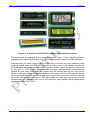
Figure 1: A Vacuum Fluorescent Display connected to the prototype PiXi
One of the initial design requirements of the PiXi was that it should be relatively easy to
connect an LCD or Vacuum Fluorescent Display (VFD) to one of the GPIO ports so that the
user can quickly use the Raspberry Pi to write text messages to a display. There are a
large number of small, low-cost LCD & VFD modules available of varying formats (e.g. 16
character x 2 line, 40 character x 2 line). Figure 1 shows a typical 2 line x 80 character
vacuum fluorescent display connected to the PiXi using an IDC cable and two IDC sockets.
The interfaces to these modules can vary widely, typically including parallel, asynchronous
serial, SPI & I2C interfaces. The LCD interface supported by the PiXi is the parallel
interface as it is one of the most widely available interfaces found on these modules. This
is not to say that LCD or VFD modules with SPI, I2C or other serial interfaces cannot be
used with the PiXi, in fact they can be used relatively easily but this example focuses on
the parallel interface variety.
The parallel interface tends to have two basic physical variations as illustrated in Figure 2,
one of which has the interface connected arranged as two rows of seven pins, the other is
arranged as one row by fourteen pins. There are also extensions to these formats that use
two extra pins (pins 15 & 16) to provide power to an LED back-light.
Astro Designs Ltd
Registered Office – Marlborough, UK
AN004.DOC 07/04/2014
AN-004 (v1.0): Connecting an LCD or VFD to the PiXi (2.0)
Page 3 of 9
Figure 2: A selection of LCD & VFD modules with parallel interfaces
The format that is supported in this example is the 2 rows x 7 pins with the option of
supporting two additional pins (pins 15 & 16) that can provide power to an LED backlight.
Important note: It's worth noting at this point that there is at least one other variation of this
interface format where the two pins used to provide power to the display module are
reversed while the remaining pins remain identical. Please check the power connections
for any LCD or VFD module are compatible with this interface before connecting the
module. It’s also worth noting that this variation can still be used with the PiXi, with a fairly
simple modification. Simply fitting the header on the display module to the opposite side of
the circuit board effectively swaps the odd & even pins on the connector, thereby reversing
the power and ground connections. This also swaps the data pins too but this can be
compensated for by setting a bit in the LCD control & data register which swaps these
signals back within the FPGA.
Astro Designs Ltd
Registered Office – Marlborough, UK
AN004.DOC 07/04/2014
AN-004 (v1.0): Connecting an LCD or VFD to the PiXi (2.0)
Page 4 of 9
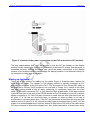
Figure 3: Location of the power connections on the PiXi and various LCD modules.
The only customisation that might be required is that the 2x7 pin header on the display
module usually needs to be fitted on the underside of the board to ensure that the power is
orientated correctly. Getting this wrong can cause the power connections to the display
module to be reversed which could damage the display module if not detected quickly so
it’s important to make sure this is right.
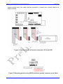
Making up the cable
There are a few options for making up the cable. Figure 4 illustrates three options for
making up the cable. The header on the display module is typically arranged as 2x7
whereas the connector at the PiXi end is 2x13. The first option is for a 26-way IDC cable to
be used with a 26-way (2x13) socket at one end and a 14-way (2x7) socket at the other
end after having peeled a strip of cable containing 14 conductors away from the main
cable. Or the same connector (2x7 or 2x8) could be fitted at both ends. If the latter method
is chosen then two of the pins of the GPIO3 header on the PiXi need to be cut off to allow a
shorter connector to fit. If the 2x8 way connector is used then the pins that need to be cut
off (pins 17 & 18) are not used and have no signals on them so there is no loss in
functionality in removing these pins. If the 2x7 way connector is fitted then the two pins that
need to be cut off (pins 15 & 16) normally provide power to the back-light (if used). For this
reason it is recommended that a 2x8 way socket is fitted at the PiXi end of the cable and a
2x7 way connector is fitted at the display end. As a further alternative, the connector at the
Astro Designs Ltd
Registered Office – Marlborough, UK
AN004.DOC 07/04/2014
AN-004 (v1.0): Connecting an LCD or VFD to the PiXi (2.0)
Page 5 of 9
display module end of the cable could be changed to a header with a socket fitted to the
display module.
Figure 4: Some examples of how to connect an LCD to the PiXi
Figure 5: Removing pins from the GPIO3 to allow a smaller connector to be fitted.
Astro Designs Ltd
Registered Office – Marlborough, UK
AN004.DOC 07/04/2014
AN-004 (v1.0): Connecting an LCD or VFD to the PiXi (2.0)
Page 6 of 9
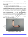
For this example, a 2x8 way IDC socket is fitted at the PiXi end of the cable and a 2x7 way
IDC socket is fitted to the display end of the cable. The following parts can be used to
make such a cable:
1. 1 x 2x8 terminal IDC socket (e.g. RS 192-7467 or Farnell 3003590);
2. 1 x 2x7 terminal IDC socket (e.g. RS 192-7451 or Farnell 3003589);
3. 1 length of 0.05” pitch, 14-way ribbon cable (typically cut shorter than 30cm) (e.g. RS 289-9852 or
Farnell 297290);
When assembling the ribbon cable into the 2x8 way socket that goes at the PiXi end of the
cable assembly, care should be taken to ensure that the coloured strand of the cable
(indicating terminal 1) is connected to terminal 1of the socket. Terminals 15 & 16 of the 2x8
way socket should have no connection in this case. Similarly, the coloured strand should
connect to pin 1 of the connector that goes at the display end of the cable assembly.
Pins 17 & 18 of the GPIO3 connector on the PiXi need to be cut-off so that a shorter 2x8
terminal IDC socket can be plugged on to the GPIO3 header. These pins are not
connected to anything on the board so this does not damage the functionality of the PiXi. If
a shorter 2x7 terminal socket is used at the PiXi end of the cable then pins 15 & 16 need to
be cut-off. Note however that by cutting off these pins the GPIO3 header will no longer be
able to provide power to a backlight.
If the display module doesn’t have a header fitted then one should be fitted. For a 2x7 way
header RS 473-8355 or Farnell 2310055 may be suitable or for a 2x8 way header RS 4738276 or Farnell 2308473 may be suitable.
Figure 6: Completed LCD / VFD cable assembly
Astro Designs Ltd
Registered Office – Marlborough, UK
AN004.DOC 07/04/2014
AN-004 (v1.0): Connecting an LCD or VFD to the PiXi (2.0)
Page 7 of 9
Using the Display
The PiXi FPGA includes an interface that allows the display to be configured and written to
using the SPI interface from the Raspberry Pi. The FPGA also has the ability to initialise
the display and write an initial message to the display immediately after the FPGA has
been configured, however this initialisation function is designed into the FPGA and can
therefore only be modified by changing the FPGA design. There is an example of how to
do this in application note AN-003 "FPGA Development on the PiXi". The default initial
message looks like this
PiXi FPGA
V. hhmmssDDMMYY
"hhmmssDDMMYY" describes the design signature for the FPGA which is based on the
time & date at which the installed design was last changed.
Character, graphics & configuration data can be written to the display by performing a
single write over the Raspberry Pi's SPI interface. The PiXi-Tools libraries, which can be
downloaded from www.astro-designs.com, provide a simple SPI read / write function that
can be executed from the command line which can be used to configure the display and
write text and potentially graphic data to the display. Other SPI interface routines may also
be used. More information on the PiXi-Tools package can be found in AN-020 "Installing
PiXi-Tools on the Raspberry Pi". In this example PiXi-Tools is used to communicate with
the display.
The full register map for the SPI interface on the PiXi FPGA can be found in AN-025
however for the purpose of using the LCD display interface only four registers are needed.
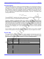
Register Map
The standard FPGA on the PiXi provides two register-mapped control & status registers for
the LCD / VFD interface which can be accessed through the SPI interface on the
Raspberry Pi. Two further registers are needed to setup the operating mode of the GPIO3
port. The display interface can be accessed over SPI at the following addresses:
Address:
0x25 [37]
0x26 [38]
0x38 [56]
0x39 [57]
Read / Write
W
W
W
W
Register Function
GPIO3 Port Configuration Register
GPIO3 Port Configuration Register
LCD / VFD Control & Data Register
LCD / VFD Configuration Register
GPIO3 Port Configuration Register
Bit(s)
Function:
(0x25) 15:0
GPIO3 bits(7:0) function select
(0x26) 31:16 GPIO3 bits(15:8) function select
LCD / VFD Control & Data Register
Bit(s)
Function:
7:0
LCD Data
8
RS
Astro Designs Ltd
Registered Office – Marlborough, UK
AN004.DOC 07/04/2014
AN-004 (v1.0): Connecting an LCD or VFD to the PiXi (2.0)
Page 8 of 9
LCD / VFD Configuration Register
Bit(s)
Function:
7:0
Not used
8
PIN_SWAP (Set this bit to swap odd/even pin functions)
15:9
Not used
The GPIO3 port can operate in several modes. Each bit can be separately configured as
input, output or a number of special functions. The LCD / VFD interface mode is one of the
special functions. The GPIO3 Port Configuration Register needs be set to a fixed value of
0x0000AAAA to select this mode, where register 0x26 should be set to 0x0000 and 0x25
should be set to 0xAAAA. This value configures all 16 bits of the GPIO3 port to the LCD /
VFD interface mode, however five bits of GPIO3 are not used for the LCD / VFD interface
mode so these bits could actually be separately configured to be used for another function.
Once the display is connected, the first thing that needs to be done is to setup the GPIO3
port to communicate with the LCD or VFD module. The following PiXi-Tools commands do
this:
pio spi-set 0 0x25 0xAAAA
pio spi-set 0 0x26 0x0000
A typical LCD display module will require an initialisation string to be sent to it to configure
the interface, position the cursor or 'write pointer' before any text can be written to the
display. The datasheet for the LCD module being used will usually describe the
configuration codes for the display. These can change from one display to another so
always check the datasheet for the display that's being used.
The following example uses PiXi-Tools "spi-set" function to send a string of data to an LCD
display to configure it prior to writing the first text:
pio spi-set 0 0x38 0x030
pio spi-set 0 0x38 0x030
pio spi-set 0 0x38 0x030
pio spi-set 0 0x38 0x038
pio spi-set 0 0x38 0x102 (Note that this sets the 'RS' bit to '1' for this command)
pio spi-set 0 0x38 0x00C
pio spi-set 0 0x38 0x001
pio spi-set 0 0x38 0x006
pio spi-set 0 0x38 0x002
And to write a message to the display:
pio spi-set 0 0x38 0x048 ("H")
pio spi-set 0 0x38 0x045 ("E")
pio spi-set 0 0x38 0x04C ("L")
pio spi-set 0 0x38 0x04C ("L")
pio spi-set 0 0x38 0x04F ("O")
pio spi-set 0 0x38 0x020 (" ")
pio spi-set 0 0x38 0x057 ("W")
pio spi-set 0 0x38 0x04F ("O")
pio spi-set 0 0x38 0x052 ("R")
pio spi-set 0 0x38 0x04C ("L")
pio spi-set 0 0x38 0x044 ("D")
Astro Designs Ltd
Registered Office – Marlborough, UK
AN004.DOC 07/04/2014
AN-004 (v1.0): Connecting an LCD or VFD to the PiXi (2.0)
Page 9 of 9
pio spi-set 0 0x38 0x021 ("!")
If all went well then the display should show:
HELLO WORLD!
PiXi-Tools also provides a more convenient way of writing to a display. The following
command writes "PiXi-Tools" to the display:
pio lcd-init
pio lcd-write "PiXi-Tools"
Or to print a message at an particular x-y position on the display, the following command
positions the same message in the centre of the first line of a 16 character wide display:
pio lcd-print 0 3 "PiXi-Tools"
Further Reading
The PiXi User Manual (UM-002) has complete information on the pin functions for GPIO3
and other interfaces on the PiXi.
If you want to learn more about programming the FPGA on the PiXi to customise the
welcome message, please take a look at application notes AN-002 "Programming the
FPGA on the PiXi" and AN-003 "FPGA Development on the PiXi".
PiXi-Tools is described in more detail in application note AN-020 "Installing PiXi-Tools on
the Raspberry Pi".
The full register map for the PiXi can be found in application note AN-025 "PiXi SPI & I2C
Register Map".
All of these documents are available for download from www.astro-designs.com.
Acknowledgements
“Raspberry Pi” is a trademark of the Raspberry Pi Foundation.
Astro Designs Ltd
Registered Office – Marlborough, UK
AN004.DOC 07/04/2014