1
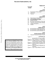
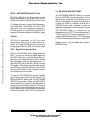
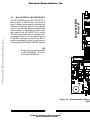
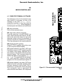
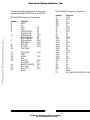
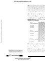
Freescale Semiconductor, Inc.
MOTOROLA
SEMICONDUCTOR
SECTION 1
TECHNICAL DATA
GENERAL DESCRIPTION
1.1 ORGANIZATION OF DATA SHEET
Advance Information
This document is composed of 4 sections. Section 1 is intended to introduce the
MC145537EVK ADPCM Codec Evaluation Kit with a brief description of the evaluation
board and a list of key features. Section 2 introduces the hardware comprising each
functional block of the MC145537EVK and the computer terminal interface. Section 3
describes the stand alone hardware operating mode and indicates a recommended
jumper positioning for this mode. It also discusses the back-to-back full duplex modes of
operation using two MC145537EVKs or one MC145537EVK with one MC145536EVK.
Section 4 describes the software interface for the computer terminal and the subroutine
commands available via the on-board MC68HC705C8P microcontroller.
Freescale Semiconductor, Inc...
MC145540 ADPCM C
EVALUATION KIT
+5V
GN
NOTE
This User's Manual - MC145537EVK ADPCM Codec
Evaluation Kit, corresponds with MC145537EVK Printed
PIEZO
Circuit Board REVISION C (XMOJOX1X92X).
SPEAKER
CLOCK GENE
CIRCUIT
1.2 INTRODUCTION
5V/3V
The MC145537EVK is the primary tool for evaluation and demonstration
of the
LEVEL SHIFT
MC145540 ADPCM Codec. The MC145537EVK provides the user with the necessary
hardware and software interface needed to access the many features and operational
modes of the MC145540 ADPCM Codec.
Figure 1-1 on the following page is a functional block diagram of the MC145537EVK.
The MC145537EVK is comprised of the MC145540 ADPCM Codec which
can operate
MC145540
Analog
from 2.7 to 5.25 volts, the 5 volt circuitry that includes the clock generation
circuitry,
ADPCM
CODECthe
Interface
MC68HC705C8P microcontroller and the MC145407 EIA232 interface, and the logic
level shifters which interface the ADPCM Codec to the clock generator and
microcontroller.
3V/5
SCP
LEVEL S
5V/3
User I/O to the board is provided via a number of convenient connectors. There are five
analog interfaces for the device: an industry standard 4-pin RJ-11 handset jack (P3) is
provided to connect the included handset, the BNC connector (P2) for the line level
transmit analog input, the BNC connector (P4) for the line level receive analog output,
the wire clamp connector (P5) for access to the auxiliary
output, and the Piezo loud
This document contains information on a new product. Specifications an
speaker which is jumper selectable to be driven by the auxiliary output. There are three
digital interfaces including the DB25 connector (P6) for the serial EIA232 interface for
the computer terminal, a 2x20 pin header (P9) for access to the ADPCM serial data and
MC145537EVK
MOTOROLA
© MOTOROLA INC., 1992
1-1
For More Information On This Product,
Go to: www.freescale.com
Freescale Semiconductor, Inc.
Freescale Semiconductor, Inc...
Paragraph
Number
TABLE OF C
Tit
1.1
1.2
1.3
SECT
GENERAL DE
Organization Of Data Sheet..................
Introduction..............................................
Features...................................................
2.1
2.2
2.3
2.4
2.5
2.6
2.7
2.8
SECT
HARDWARE D
Power Supply Configurations ...............
Clock Generation Circuitry....................
MC145540 ADPCM Codec...................
MC68HC705C8P....................................
MC145407 and EIA232 Port Descripti
Computer Terminal Interface Descript
Jumper Descriptions ..............................
Handset....................................................
3.1
3.2
3.3
SECT
OPERATING CO
MC145537EVK Single Board Analog
MC145537EVK to MC145537EVK Fu
MC145537EVK to MC145536EVK Fu
4.1
SECT
MICROCONTROLLER SOF
Computer Terminal Software Comma
Figure 1-1.
LIST OF ILLU
MC145537EVK Functional Block
Figure 2-1.
DSW1
Settings
for Transcoding
Motorola reserves the right to make changes without further
notice
to any
products
Figure
2-2.
Jumper
Positions
herein to improve reliability, function, or design. Motorola does not assume any liabilityfor Switching T
EIA-232
Serial
Computer Termin
arising out of the application or use of any product or circuit described
herein;
neither
Figure
3-1.
Jumper
Settings
for Digital Loopb
does it convey any license under its patent rights nor the rights of others. Motorola
Figure
3-2. devices
Recommended
Configuration for
products are not authorized for use as components in life
support
of systems
Operation
........................................
intended for surgical implant into the body or intended to support or sustain life. Buyer
Figure
3-3. Recommended
Configuration for
agrees to notify Motorola of any such intended end use
whereupon
Motorola shall
Operation
........................................
determine availability and suitability of its product or products for the use intended.
Figure
4-1. Input
Modes of the MC1
Motorola and µ are registered trademarks of Motorola, Inc.
Motorola,
Inc./ Output
is an Equal
Employment Opportunity/Affirmative Action Employer
MC145537EVK
MOTOROLA
MOTOROLA
ii
i
For More Information On This Product,
Go to: www.freescale.com
Freescale Semiconductor, Inc.
the controlling clocks, and a 2x16 header
SECTION 2
signals.
HARDWARE DESCRIPTION
The MC145537EVK is powered by the three
at the top of the circuit board. This evaluatio
clock generator, microcontroller and EIA232
NOTE
be powered
by this 5 volt supply as selected
Please refer to the MC145537EVK Schematic
for discussion
2.7
volts
to
5.25
volts that is also applied at P
of the hardware.
Freescale Semiconductor, Inc...
2.1 POWER SUPPLY CONFIGURATIONS
+5V
The MC145537EVK is powered by the three terminal wire clamp connector, P7 located
at the top of the circuit board. This evaluation board requires a +5V supply to power the
clock generator, microcontroller and EIA232 port. The MC145540 ADPCM Codec may
be powered by this 5 volt supply as selected by jumper J2 or by an additional supply of
PIEZO
2.7 volts to 5.25 volts that is applied at the third terminal of P7.
SPEAKER
The MC145540 powers-up from a hardware reset (S3) in a mode with the on-chip
charge pump running. This allows the device to operate with a power supply as low as
2.7 volts to as high as 5.25 volts. For 5 volt operation, jumper J2 should be left in the 5V
position. This selects the 5 volt power supply terminal of P7 to be connected to the
VEXT pin of the MC145540. The charge pump may be turned off or left running. 5V/3V
CLOCK G
CIRC
LEVEL SHIFT
For lower voltage applications (i.e. 3 volts), jumper J2 should be moved to the 3V
position, and jumper J1 should be in the position marked 3EXT. This jumper
configuration connects the MC145540 VEXT pin and the logic level shifting circuitry to
the third terminal of P7 so that the MC145540 may be powered from an off-board lower
voltage power supply.
Analog
MC145540
Jumper J12 allows the MC145540 to be connected to eitherInterface
of the 5 volt supply
ADPCM(VCC),
CODEC
or the lower voltage supply (VDD). This jumper should be left in the VDD position
except to insert an ammeter for measuring the current of the MC145540 only.
S
LEV
Jumper J13 connects the MC145540 VDD pin (VDDA) to the VEXT pin for 5 volt
applications with the charge pump turned off.
Figure 1-1. MC145537EVK
2.2 CLOCK GENERATION CIRCUITRY
A 20.48 MHz crystal oscillator is used as the System Clock for the MC145537EVK.
From this 20.48 MHz crystal, Frame Sync (FSYNC), Bit Clock (BCLK), and Signal
Processor Clock (SPC) are derived for use by the MC145540.
MC145537EVK
MOTOROLA
MOTOROLA
1-2
2-1
For More Information On This Product,
Go to: www.freescale.com
Freescale Semiconductor, Inc.
MC145540 Features (cont.)
1.3 FEATURES
•
Low Noise, High Gain, Three T
Interface
•
Push-Pull 300Ω Power Drivers
Interface
Freescale Semiconductor, Inc...
GENERAL
•
Provides Stand Alone Evaluation on Single Board
•
The kit provides analog to analog, analog to digital• (64 kbps
PCM, 300Ω Auxiliary Outpu
Push-Pull
32 kbps ADPCM, 24 kbps ADPCM, CCITT G.726 16 kbps ADPCM and
Motorola proprietary 16 kbps ADPCM), or digital (64
PCM, Regulated
32 kbps Charge Pum
• kbps
Voltage
ADPCM, 24 kbps ADPCM, CCITT G.726 16 kbps ADPCM
and
Motorola
Voltage Applications
proprietary 16 kbps ADPCM) to analog connections.
•
Receive Side Noise Burst Dete
+5 Volt Only Power Supply or 5 Volts Plus 2.7 to 5.25 Volt Supply.
•
Custom DSP Engine Optimized
Easily Interfaced to Test Equipment, Customer System, Second
MC145537EVK or MC145536EVK (for 5 volt operation only) for Full
Duplex Operation.
•
•
•
Convenient Access to Key Signals
•
Piezo Loud Speaker
•
EIA232 Serial Computer Terminal Interface for Control of the MC145540
ADPCM Codec Features.
•
Compatible Handset Provided
•
Schematics, Data Sheets, and User's Manual Included
MC145540 Features
•
Single 2.7 to 5.25 Volt Power Supply
•
Typical 3 Volt Power Dissipation of 65 mW, Power Down of 0.1 mW
•
Differential Analog Circuit Design for Lowest Noise
•
Complete Mu-Law and A-Law Companding PCM Codec/Filter
•
Conforms to CCITT and ANSI Standards for ADPCM Transcoding at 64,
32, 24 and 16 kbps data rates
•
Universal Programmable Dual Tone Generator
•
Programmable Transmit Gain, Receive Gain and Sidetone Gain
MC145537EVK
MOTOROLA
MOTOROLA
1-4
1-3
For More Information On This Product,
Go to: www.freescale.com
Freescale Semiconductor, Inc.
2.4 MC68HC705C8P
FSYNC - Frame Synchronization Pulse
DSW1 allows
thethat
userare
to select
the "width
The MC145537EVK is designed to accommodate additional
features
not
cycles.
The the
individual
switches
currently supported by the resident software. Three examples
include
two LEDs
(D6 of DSW1
resistors
areaccess
connected
and D7), the push button switch (S1) and the 2x16 header
(P8). P8that
gives
to theto the inputs o
of parallel
DSW1 is
loaded into the shift r
MC145540 reset pin, the MCU reset pin, SCP control portThe
and value
an 8-bit
port.
BCLK signal. The inputs of this shift r
microcontroller using the FW (Frame sync
section 3 for the software command set. NO
be in the open position and that the microc
open to this node for the clock circuit to oper
Figure 2-1 below indicates the proper dip sw
and 16 kbps long frame clocking, and 32 kb
For 64 kbps operation, switches 1, 2 and 3
output of the shift register has only one ris
load / shift cycle. Refer to the MC145540 Da
64kbps
32kbps
24k
DSW1
--->
DSW1
--->
DS
-1 2
ON
1 2
ON
1 2
3
4 5
6
7
8
8
8
7
7
6
6
4 5
4 5
3
3
Freescale Semiconductor, Inc...
Sync (FSYNC)
thea 8 kHz signa
The MC68HC705C8P is one of Motorola's popular 8-bitFrame
microcontrollers
which ishas
(PCM) words. The
ADPCMThe
transcoding rate
Serial Peripheral Interface port (SPI) and an asynchronous
interface.
controlled bySerial
the width
of the
MC145537EVK utilizes the SPI port for interface to the MC145540's
Control
Portframe sync me
pins9600
respectively.
and FSR signals
(SCP). The asynchronous interface is used for the EIA-232
bps serialThe
portFST
for the
ADPCM
Codec routine
to determine
computer terminal interface. The microcontroller executes
a monitor
which the sample r
analog conversions.
FSYNC
is presented to
supports sixteen commands for programming and monitoring
the status
of the
the MC145540 for FSR pin and FST pin resp
MC145540 ADPCM Codec.
The position of this
switch is Open / Off.
Figure 2-1. DSW1 Setting
MC145537EVK
MOTOROLA
MOTOROLA
2-2
2-5
For More Information On This Product,
Go to: www.freescale.com
Freescale Semiconductor, Inc.
2.3 MC145540 ADPCM CODEC
Freescale Semiconductor, Inc...
BCLK - ADPCM/PCM Data Bit Clock
The MC145540 ADPCM Codec is a single
Bit Clock (BCLK) is the Clock that controls the ADPCM/PCM
bit ADPCM
transfers.encoder/decoder
The BCLK
and an
and th
signal is presented to J6-B and J6-C for selected use by the
MC145540
ADPCM
Codec
applications requiring the digitization and
for bit clock receive (BCLKR) and for bit clock transmit (BCLKT)
devicerespectively.
is designed to operate over a wide vo
is ideal for battery powered as well as A
P1 allows the user to select the frequency of BCLK. The ADPCM
jumper selectable
frequencies
Codec also
includes a serial co
are 2.048 MHz, 1.024 MHz, 512 kHz, 256 kHz, 128 kHz,registers
and 64 kHz.
It
is
important
to
that permit a microcomputer
to exe
note that only one frequency should be selected at any time. The duration of the
FSYNC signal is controlled by the BCLK clock cycles, but
theADPCM
frequency
of FSYNC
is
The
Codec
is designed
to me
always 8 kHz when either of the BCLK frequencies is selected.
requirements of CCITT Recommendation G
T1.303 and CCITT Recommendation G.72
256kHz
16 kbps ADPCM standard, CCITT Recomme
PCM conformance specification of the CCITT
256 kHz is presented to J6-A for connection to BCLKR for use as the internal
sequencing clock for the codec-filter and charge pumpPlease
functions
of to
thethe
device.
The data sheet f
refer
included
option for using BCLKR as the source for the internal 256
kHz sequencing
clock must
ADPCM
Codec.
be programed via the SCP port at byte register zero, bit 7.
SPC - Signal Processing Clock
SPC is a 20.48 MHz clock signal presented to the MC145540 signal processor clock
(SPC, 21) pin for use as its digital signal processor clock. There are several options for
the SPC which are controlled by jumpers J17, J8 and J18. It is important to note that J8
should not be selected when J18 is selected, only one of these jumpers should be on
the evaluation board at the same time. J17 selects the on-board 20.48 MHz clock to
drive the SPC pin of the MC145540. J8 selects a buffered 20.48 MHz to be output to the
P9 header. This allows the on-board oscillator to be used off of the board. J18 connects
the SPC pin of the MC145540 to the P9 header pins to allow an external SPC clock to
drive the MC145540. If an off-board clock is used for SPC, then both J17 and J8 should
be removed from the board.
To use two MC145537EVK boards together for full duplex audio, J17 is used and J8
and J18 are removed from the boards. This configuration is also good for use with an
MC145536EVK which has the MC145480 5 volt PCM Codec-Filter and MC145532
ADPCM Transcoder. When two MC145537EVK boards are connected together with a
ribbon cable that is about 2 inches (about 5 centimeters), one 20.48 MHz clock may be
used for both evaluation boards. The jumpers will not be the same for both boards. The
20.48 MHz clock may feed-through to the other board via the ground circuit and cause
noise, which may be eliminated by externally connecting a wire to one side of R3 of one
board to the other side of R3 of the other board.
MC145537EVK
MOTOROLA
MOTOROLA
2-4
2-3
For More Information On This Product,
Go to: www.freescale.com
Freescale Semiconductor, Inc.
J10
J11
J12
J14
J15A,B
J16
J18
Connects the SPC pin of the MC145540 to the 40 pin header connecter,
P9. This jumper must be removed if jumper J8 is connected.
C31
Connects the level shifted 3 volt 20.48 MHz on-board oscillator to the
MC145540 SPC pin and to the buffers for off-board use. This jumper must
be removed if the SPC pin is to be driven by an external clock.
P6
C30
J17
C33
C35
C34
C32
MC145407
Freescale Semiconductor, Inc...
J13
Invert TX and RX circuits to / from EIA-232 connecter
2.5 MC145407
(P6) for
and
proper
EIA232 PORT DESCRIP
operation
The MC145407 is a single 5 volt power sup
Forces the microcontroller into a continuous receivers
reset state.
in addition to an on-chip voltage
develops the drive voltages to satisfy the E
Connects the VEXT pin of the MC145540 to the
the level
powershifting
supply and signal conditioning to
independent of the level shifters and MC145540
resetanpull-up
resistor.
produce
EIA-232
serial This
port which operat
accommodates current measurements for the
MC145540.
This
jumper
controlled
by the
microcontroller's
crystal.
should usually be connected to the VDD position.
MC145540 configuration and control da
Connects the MC145540 pin VDD to its power
supply pin VEXT.
is
MC145537EVK
via aThis
computer
terminal. An
used only when the MC145540 is used at 5 volts
and the
on-chip
charge
connector
(board
side)
and the appropriate
pump must be disabled by programming theserial
MC145540
at byte
registeris the 3 wire minim
computer
interface
zero, bit 2.
data, receive data and signal ground. Only
connected. Upon turning on the board, or p
Connects either RO or PO- as analog outputmessage
from MC145540
to the BNC
should appear
on the screen:
connecter P4
Motorola MC145537EVK Evaluation KI
J15A connects the AXO- signal to wire clamp
connector P5. J15B
MC145540>
connects the AXO- signal to the piezo speaker SP1.
Where X.X represents the software revision
This jumper is a control input to the microcontroller. It is intended to tell the
microcontroller that two MC145537EVK boards
are
connected
together
at
If the
computer
terminal
is configured
correc
the 32 pin header connecter P8 so that one microcontroller
control
the MCU reset may
switch
is released, then the t
both MC145540 ADPCM Codecs, thus eliminating
the need
for more
than
the DB-25
connecter)
may
need to be exch
one computer terminal. This option is not presently
supported
thejumpers J10-A, J10-B
This may
be donebyby
microcontroller software. The user may use this
a control
input for options.
two as
jumper
configuration
software development.
-->
J10ABCD
MCU RESET
R
1
7
C
2
6
C10
Figure 2-2. Jumper Positions for Switch
EIA-232 Serial Compu
MC145537EVK
MOTOROLA
MOTOROLA
2-6
2-9
For More Information On This Product,
Go to: www.freescale.com
Freescale Semiconductor, Inc.
2.6 COMPUTER TERMINAL INTERFACE DESCRIPTION2.7 JUMPER DESCRIPTIONS
The serial computer terminal interface uses only transmitThe
data,
following
receive table
data and
shows
signal
all on-board jum
ground. These signals are on circuits 2, 3 and 7 of the DB-25.
Please See
reference
the section
the schematic
on the for additiona
MC145407 and EIA-232 port for reconfiguring the circuits for pin 2 and pin 3. The
Jumper
Functionality
computer terminal should be configured for:
1. 9600 bps (bits per second or 9600 baud)
J1
If VDD is selected for 3 volts by
+3 volt power supply input of P
from the 5 volt supply.
J2
Sets VDD power supply of the
power supply wire clamp conne
for the logic level shifters and t
J3
Connects the on-board 20.48 M
generate the 8 kHz FST, bit clo
allows these clocks to be deriv
J4
Connects the on-board 20.48 M
logic level shifter for driving the
MC145540. This jumper allows
oscillator to clock the SPC pin
J5A,B
Connects the 8 kHz FSYNC on
respectively of the MC145540.
J6A,B,C
J6A connects the on-board 256
MC145540 for use as the intern
pin as the input for an external
be selected by programming th
and J6C connect the on-board
J7A,B
Connects the on-board 256 kH
40 pin header connecter, P9. T
PCM Codec-Filter on an MC14
MCLK function is similar to the
of the MC145540.
J8
Connects a buffered on-board
pin header connecter, P9 for of
connected if Jumper J18 is con
SPC pins of P9.
J9
Connects the ADPCM / PCM o
ADPCM / PCM input (DR pin)
operation.
2. Full-duplex
Freescale Semiconductor, Inc...
3. 8-Bit data words
4. 1 stop bit
5. Parity should be turned off
6. Linefeed automatic with return
MC145537EVK
MOTOROLA
MOTOROLA
2-8
2-7
For More Information On This Product,
Go to: www.freescale.com
Freescale Semiconductor, Inc.
3.2
MC145537EVK to MC145537EVK Full-Duplex Analog
2.8 HANDSET
End-to-End
Freescale Semiconductor, Inc...
The compatible
handset
included with th
The MC145537EVK evaluation boards were designed to connect
back-to-back.
A 2x20
W3-K-EM-80,
reverse
polarity.
The hands
header connecter with a ribbon cable, 36 inches (about one meter) maximum in length,
The handset
incorporates a low
makes the necessary electrical connections allowing a fullconnector.
"analog-to-analog",
"handsetequipped
a hearing aid coil and
to-handset" path to be established. The three volt supply isreceiver
not connected
to with
the ribbon
cable and therefore the MC145537EVK should be operated at 5 volts for logic level
TRANSMITTER
compatibility with maximum digital noise immunity between
the two MC145540 ADPCM
Codecs.
Transmit Output Level @ 1000 Hz: -46 dBV
Output Impedance @ 100 Hz: 1000 ± 300Ω
NOTE
Power (5 volt) and Ground are bussed from one
RECEIVER
MC145537EVK to the second MC145537EVK.
Do not
connect a second power supply to the second
Receive Output Level @ 1000 Hz: 79 dBSPL
MC145537EVK!
Receive Input Impedance @ 100 Hz: 150 Ω
For more detailed characteristics of the W3
Equipment Corporation in North America at 1
MC145537EVK
MOTOROLA
MOTOROLA
2-10
3-3
For More Information On This Product,
Go to: www.freescale.com
Freescale Semiconductor, Inc.
C10
J11
C8
C7
C6
J4
J3
C3
U3
CLK
GEN
C5
5V
3V
J2 VDD
C1
DSW1
RP1
--->
U1
D2
C2
U2
+5V GND +3V
D4
3EXT
3REG
J1
C11
AXO>P5
AXO>SP
J15AB
R26
P2
(enables digital loopback)
(EIA-232 cable dependent, swaps Tx
and Rx pins to DB-25 connector)
P5
PIEZO
SPEAKER
OUT
C9
MCU RES
VDD
VDDA
RO
AXO>P5
AXO>SP1
BACK TO BACK
SPC CLK
SPC OFF
2048
RN1
R D
1 1
J11
J12
J13
J14
J15A
J15B
J16
J17
J18
P1
MC74HC393
REVISION-C
XMOJOX1X92X
IN
IN
IN
IN
OUT
IN
IN
OUT
OUT
OUT
IN
MC145537EVK
CLK GEN
SPC
FSYNC>FSR
FSYNC>FST
256k>BCLKR
BCLK>BLKCR
BCLK>BCLKT
BCLK>MCLK
256k>MCLK
SPC>P6
DT>DR
TOP ROW
MC74HC390N
UT
J3
J4
J5A
J5B
J6A
J6B
J6C
J7A
J7B
J8
J9
J10
MC145537EVK
Notes
(dependent on +3V source)
(dependent on desired MC145540
supply voltage)
048
024
512
256
128
64
Position
3EXT
5V
SPC
MC74HC165N
The following table shows all on-board jumpers and their corresponding positions for
MC74HCU04
digital loopback which accommodates analog end-to-end operation.
Jumper
J1
J2
R
C
2
6
R R
3 2
0 9
C12
D DR
3 5 2
U4
R4
R3
S2
J10ABCD
C13
MC145537EVK SINGLE BOARD ANALOG END-TO-END OPERATION
C4
C30
C32
20.48
MHZ
R R
2 2 -->
8 7
C34
Y1
MCU RESET
C31
C33
Freescale Semiconductor, Inc...
R
1
7
C35
The following information describes the "most common" configurations that the
MC145537EVK may operate. There are many configurations of operation that have not
MC145407
been described in this document that the user may find useful. Please
familiarize
yourself with the included schematic diagram as this may provide insight into a
configuration that may prove beneficial for evaluating these parts in your application. If
there are specific questions on a particular configuration that is not documented, do not
hesitate to contact your local Motorola Representative, or call the factory for assistance.
3.1
P8
P6
P9
SECTION 3
OPERATING CONFIGURATIONS
OUT
OUT
IN
OUT
IN
OUT
Figure 3-1. Jumper Settings for Digital L
MOTOROLA
MOTOROLA
3-2
3-1
For More Information On This Product,
Go to: www.freescale.com
Freescale Semiconductor, Inc.
MC145537EVK to MC145536EVK Full-Duplex Analog End-to-End
MC145537EVK
Board #1
Freescale Semiconductor, Inc...
3.3
The MC145536EVK and MC145537EVK evaluation boards were designed to connect
back-to-back. A 2x20 header connecter with a ribbon cable, 2-3 inches maximum in
length, makes the necessary electrical connections allowing a full "analog-to-analog",
"handset-to-handset" path to be established. The 20.48 MHz oscillators may cause
noise in the grounds between these boards resulting in a beat frequency tone in the
audio channel. To eliminate this noise, use a jumper clip wire to connect one terminal of
the crystal on the MC145537EVK to one terminal of the crystal on the MC145536EVK.
This will synchronize the two crystals and eliminate the beat component. This noise is
not present when a 36 inch (about one meter) ribbon cable is used and the on-board
20.48 MHz oscillator is used for the SPC on the MC145536EVK. The MC145537EVK
must be operated at 5 volts for logic level compatibility between the MC145540 ADPCM
Codec and the MC145532 ADPCM Transcoder.
NOTE
Power and Ground are bussed from the MC145537EVK to
the MC145536EVK. Do not connect a second power supply
to the MC145536EVK!
Figure 3-2. Recommended Cabling
Oper
MC145537EVK
MOTOROLA
MOTOROLA
3-4
3-7
For More Information On This Product,
Go to: www.freescale.com
Freescale Semiconductor, Inc...
Freescale Semiconductor, Inc.
The following table shows all on-board jumpers and their corresponding positions for
connecting one MC145537EVK to a second MC145537EVK
full-duplexfor
analog
Jumper for
Configuration
second (clock rece
operation.
Jumper
Position
Jumper Configuration for first (clock generator) MC145537EVK.
J1
3EXT
J2
5V
J3
CLK
IN
Jumper
Position
Notes
J4
SPC
IN
J1
3EXT
Not applicable
J5
FSYNC>FSR
OUT
J2
5V
5 volt operation
recommended
FSYNC>FST
OUT
J3
CLK
IN
J6
256>BCLKR
OUT
J4
SPC
IN
BCLK>BLKCR
OUT
J5
FSYNC>FSR
IN
BCLK>BCLKT
OUT
FSYNC>FST
IN
J7
BCLK>MCLK
OUT
J6
256>BCLKR
OUT
256>MCLK
OUT
BCLK>BLKCR
IN
J8
SPC>P6
OUT
BCLK>BCLKT
IN
J9
DT>DR
OUT
J7
BCLK>MCLK
OUT
J10
TOP ROW
256>MCLK
OUT
J8
SPC>P6
OUT
J11
MCU RES
OUT
J9
DT>DR
OUT
J12 dependent,
VDDswaps Tx
J10
TOP ROW
(EIA-232 cable
J13
VDDA
OUT
and Rx pins
to DB-25 connector)
J14
RO
J11
MCU RES
OUT
J15
AXO>P5
OUT
J12
VDD
AXO>SP1
IN
J13
VDDA
OUT
J16
BACK TO BACK
OUT
J14
RO
J17
SPC CLK
IN
J15
AXO>P5
OUT
J18
SPC OFF
OUT
AXO>SP1
IN
P1
2048
J16
BACK TO BACK
OUT
J17
SPC CLK
IN
J18
SPC OFF
OUT
P1
2048
MC145537EVK
MOTOROLA
MOTOROLA
3-6
3-5
For More Information On This Product,
Go to: www.freescale.com
Freescale Semiconductor, Inc.
Freescale Semiconductor, Inc...
4.1 COMPUTER TERMINAL SOFTWARE COMMAND SET
MC145536EVK
Board #2
SECTION 4
MICROCONTROLLER SOFTWARE COMMAND SET
The following is a list of all commands currently available, along with an explanation on
their function. In all cases, an error in the command entry will be signalled by the
message on the CRT: Error: unknown command. In addition, if the number of
parameters specified is less than what the command requires, the message Error:
parameter(s) input will be displayed on the computer terminal display. The monitor
routine expects all numbers and coefficients to be in hexadecimal form.
HE (Help command)
Print out the command menu.
RE <logic state> (Reset command)
Force the reset line to the MC145540 to whichever state has been specified by logic
state. Recall that the reset line into the MC145540 is an active low line, i.e., the part is
held in the reset state when the logic state is specified as zero. For a valid reset and
reactivate cycle to occur,this command must be executed twice. Once for setting the
reset pin low (RE 0), followed by a command to take the reset pin high again (RE FF)
This is an alternative to the reset pushbutton switch, S3.
DR (Display all SCP registers)
Read all 10 SCP registers (plus silicon mask register BR15) and display their contents
on the computer terminal display.
SC [register address] <scp data> (SCP access command)
Execute an access to SCP register specified by register address. If scp data is included,
it is written to the register; otherwise, the access is to read the register. In either case,
the contents of the register after the access is completed are displayed at the computer
terminal display. This command allows full manipulation of the control registers. To
display the status of byte register 2, (SC 2). To turn on the AXO+ and AXO- driver pair,
(SC 2 40). This command will also program the dc bias voltage for the RO, PO-, PO+,
PO-, AXO+ and AXO- outputs to half of the VEXT voltage. This command will always
program all of the accessed byte register's functions.
SS [register address] <scp data> (SCP access command)
Same as the SC command explained above, except it continuously accesses the SCP
interface, whether for read or write. This is useful in debugging situations, in which it is
necessary to synchronize some test equipment with an access
the Recommended
SCP interface. Configuratio
Figureon3-3.
This successive read is terminated when the Tone Demo switch, S1 or the
Oper
microcontroller reset switch, S2 is depressed.
MC145537EVK
MOTOROLA
MOTOROLA
3-8
4-1
For More Information On This Product,
Go to: www.freescale.com
Freescale Semiconductor, Inc...
Freescale Semiconductor, Inc.
The following table shows all on-board jumpers and their corresponding
MC145536EVKpositions
Jumper for
Configuration
connecting an MC145537EVK to an MC145536EVK for full-duplex operation.
Jumper
Position
MC145537EVK Jumper Configuration
J1
OUT
J2A
OUT
J2B
IN
Jumper
Position
Notes
J3A
OUT
J1
3EXT
Not applicable
J3B only
IN
J2
5V
5 volt operation
*J4
OUT
J3
CLK
IN
J5
OUT
J4
SPC
IN
J6
OUT
J5
FSYNC>FSR
IN
J7
IN
FSYNC>FST
IN
J8
IN
J6
256>BCLKR
OUT
*J9
OUT
BCLK>BLKCR
IN
*J10
OUT
BCLK>BCLKT
IN
J11A
IN
J7
BCLK>MCLK
OUT
J11B
OUT
256>MCLK
OUT
J12A
IN
J8
SPC>P6
OUT
J12B
OUT
J9
DT>DR
OUT
J13A dependent,
IN swaps Tx
J10
TOP ROW
(EIA-232 cable
J13B
OUT
and Rx pins
to DB-25 connector)
J14A
OUT
J11
MCU RES
OUT
J14B
IN
J12
VDD
J15A
IN
J13
VDDA
OUT
J15B
OUT
J14
RO
J16
IN
J15
AXO>P5
OUT
J17
IN
AXO>SP1
IN
J18
IN
J16
BACK TO BACK
OUT
J19
IN
J17
SPC CLK
IN
J20
OUT
J18
SPC OFF
OUT
P1
2048
P1
2048
S1
ALL SWITCHES OPEN / CLOC
MC145537EVK
MOTOROLA
MOTOROLA
3-10
3-9
For More Information On This Product,
Go to: www.freescale.com
Freescale Semiconductor, Inc.
Freescale Semiconductor, Inc...
ME [memory address] <memory data> (Mem
Access the memory location specified by m
microcontroller operates in internal memor
goes from 0 to HEX 1FFF. If the address sp
and a memory data field has been includ
location, otherwise the memory location is re
memory location after the access has been c
TG [coefficient] [attenuation] [tone generator
Program the tone generation function of the
field, with the coefficient and attenuation i
debugging aide, all SCP accesses required
displayed on the screen. e.g. TG 100 200
generator to a frequency of 697 hertz at an
amplitude would be (TG 6D5 200 1). Th
sequence of SC commands:
SC 7
'REM Read BR7
(SC 7) OR HEX 08 'REM Logical OR
'REM Let BR7=H
SC 7 08
'REM Write HEX
SC 4 D5
'REM Write lower
SC 5 06
'REM Write to ton
'REM write the m
'REM coefficient i
SC 7
'REM Read BR7.
Is (SC 7) < HEX 80 'REM Check that
'REM read BR4 a
SC 4 00
'REM Write the le
'REM coefficient i
SC 5 42
'REM Write to ton
'REM write the m
'REM coefficient i
SC 7
'REM Read BR7.
Is (SC 7) < HEX 80 'REM Check that
'REM read BR4 a
SC 7 0A
'REM Turn on ton
MA <encoding mode> (Encoding law comma
If an encoding mode field is specified, set th
or A-law encoding (encoding mode = 1). O
used.
E2 [256 kHz clock option] (External 256 kHz
Literature Distribution Centers:
Set
or reset the external 256 kHz clock op
USA: Motorola Literature Distribution; P.O. Box 20912; Phoenix, Arizona
85036.
EUROPE: Motorola Ltd.; European Literature Center; 88 Tanners Drive,
Blakelands,
Milton
Keynes, MK14 1
5BP,
clock
option
parameter:
toEngland.
set the option, 0
ASIA PACIFIC: Motorola Semiconductors H.K. Ltd.; P.O. Box 80300; Cheung Sha Wan Post Office; Kowloon Hong Kong.
JAPAN: Nippon Motorola Ltd.; 3-20-1 Minamiazabu, Minato-ku, Tokyo 106 Japan.
MOTOROLA
4-2
For More Information On This Product,
Go to: www.freescale.com
Freescale Semiconductor, Inc.
Freescale Semiconductor, Inc...
IO <I/O mode>
status of the DSW1 and if any of DSW1's s
Set or display the I/O mode of the part, represented by anot
twotry
bittonumber,
drive the
IOMode(1:0).
shift register. If the param
This command allows easy access to the four I/O modesmicrocontroller
of the MC145540.
will not
Thetrytable
to program the s
below summarises these modes. Please refer to the
open
data
the sheet
clock circuit
for additional
will generate an FSYN
information.
The microcontroller may be used to shorten
the value of the FW parameter to other than
load that parameter into the shift register, p
closed. The value of Frame sync pulse wi
I/O Mode(1:0)
MC145540 Mode
HEX 80 to HEX FF, or else the number 0. A
kbps; HEX F0 puts the board into 32 kbps;
00
ADPCM Codec
C0 puts the board into 16 kbps; HEX 80 puts
01
PCM Codec
10
CCITT Test
11
Battery Test
Figure 4-1. Input / Output Modes of the MC145540 ADPCM Codec
CD <Charge pump option>
Set or reset the charge pump disable option via an SCP write access. CD 0 will enable
the operation of the charge pump; CD 1 will disable it.
ST <Sidetone Gain>
Set or display the gain factor to be applied to the sidetone signal from the transmit filter
of the Codec section of the part to the sample & hold register in the receive path of the
Codec. Numbers in the range of 0 to 7 are expected.
XG <Transmit Gain>
Set or display the gain factor to be applied to the transmit signal before it is input to the
transmit filter. Numbers in the range of 0 to 7 are expected.
AG <Analog Receive Gain>
Set or display the gain factor to be applied to the receive signal before in is input to the
receive filter of the Codec section of the part. Numbers in the range of 0 to 7 are
expected.
DG <Digital Receive Gain>
Set or display the gain factor to be applied to the received data, after it has been
processed by the decoder function in the DSP engine. Numbers in the range of 0 to
HEX 7F are expected.
FW [Frame sync pulse width]
The width of the sync pulse to be applied to the MC145540 can be set by either the DIP
switch DSW1, or by the on-board microcontroller. DSW1 and the microcontroller have
access to the input of the parallel loaded shift register. The microcontroller reads the
MC145537EVK
MOTOROLA
MOTOROLA
4-4
4-3
For More Information On This Product,
Go to: www.freescale.com