1
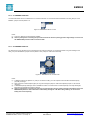
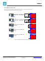
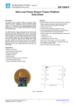
EM MICROELECTRONIC - MARIN SA EM8500 EMEVB8500 EVALUATION BOARD USER MANUAL Description The EMEVB8500 board is targeted at rapid evaluation and prototyping of integrated energy harvesting solutions based on EM8500 family of devices. The evaluation board offers a set of features to show the performance of EM8500 hardware applications. The EMEVB8500 board allows flexibility with various configuration, external harvester input, internal or external storage elements and user connections. Main Features Hardware Software Long Term storage selection (on-board Supercap or external) EMPB85xx Software is available when the configuration tool EMPB85xx is used. Supercap discharge path Refer to EMPB85xx User Manual. Short term storage selection (on-board capacitor or external) External harvester selection Expansion header for prototyping and external connection Configurable wake-up line with push-button EM8500 I2C pull-up selection Copyright 2015, EM Microelectronic-Marin SA EMEBV8500-MN01, Version 1.0, 28-Sep-15 1 PRELIMINARY www.emmicroelectronic.com 420005-A01, 2.0 EM8500 1. OVERVIEW The architecture of the EMEVB8500 is based on the following block diagram S1 J2A J1 LX1 User HRV VDD_LTS VDD_HRV EM8500 H3 Miscs STS VDD_USB I2C pull J6A-J6B H2 Com Ctrl WAKE-UP CONFiG Push-button JA4-J4B J5A-J5B VDD_STS VSS VSS_DCDC I2C - SPI BAT_LOW HRV_LOW WAKE_UP VAUX_GND2 VAUX_GND1 VAUX_GND0 VSUP VAUX2 VAUX1 VAUX0 J2B J3 S2 Supercap User LTS S3 STS User STS UserH1STS STS Supply User extension connector User extension screw terminal block Configuration area Figure 1-1 EMEVB8500 System Architecture Copyright 2015, EM Microelectronic-Marin SA EMEBV8500-MN01, Version 1.0, 28-Sep-15 2 PRELIMINARY www.emmicroelectronic.com 420005-A01, 2.0 EM8500 2. EMEVB8500 BOARD 2.1. DESCRIPTION The board is equipped with: EM8500 core design consisting of the EM8500 devices and required external components. Extension header (H1) used to supply the application Extension header (H2) used to interface the communication and control signals between application and EM8500. Extension header (H3) used to expose other signals (STS, LTS, HRV, USB ...) Extension header (PRG) used to configure the EM8500 Terminal block (S1) to connect any external harvester Terminal block (S2) to connect an external Long Term Storage to LTS (primary or secondary storage) Terminal block (S3) to connect an external Short Term Storage to STS Supercap (SC) as LTS with a dedicated discharge path Different jumper areas to select the terminal blocks or internal board resources and configure I2C lines or Wake-up line Push button (K2) used for the Supercap discharging Polarity configurable push button (K1) used for Wake-up control line. The board dimension is 65 x 65 mm. H1, H2 and H3 are male headers 2x10 pins (2.54 mm pitch). PRG is male headers 2x4 pins (2.54 mm pitch). S1, S2 and S3 are 2 pins screw terminal block (3.5 mm pitch). Copyright 2015, EM Microelectronic-Marin SA EMEBV8500-MN01, Version 1.0, 28-Sep-15 3 PRELIMINARY www.emmicroelectronic.com 420005-A01, 2.0 EM8500 PRG 8500 VSS CS VSUP SCL AVDD_STS MISO WAKE_UP MOSI_SDA K2 Press K2 for Supercap (SC) safe discharge 1 2 3 4 5 6 7 8 S1 – J1 Place jumper on J1 to connect the external Harvester (S1) S2 – SC – J2A – J2B Place jumper on J2A to connect the external LTS (S2) Place jumper on J2B to connect the internal LTS Supercap (SC) S3 – J3 B Configuration for Wake-up button (K1) - rising edge Configuration for Wake-up button (K1) - falling edge 1,2 3,4 5,6 7,8 9,10 11,12 13,14 15,16 17,18 19,20 WAKE-UP H3 VSS AVDD_STS VSS AVDD_LTS VSS AVDD_USB AVDD_REG AVDD_HRV VSS VSS Place jumper on J3 to connect the external STS (S3) 1,2 3,4 5,6 7,8 9,10 11,12 13,14 15,16 17,18 19,20 H1 VSS VSUP VAUX_2 VAUX_1 VAUX_0 VSS VAUX_GND_0 VAUX_GND_1 VAUX_GND_2 VSS 1,2 3,4 5,6 7,8 9,10 11,12 13,14 15,16 17,18 19,20 H2 VSS CS SCL (SCK) MISO (SDO) MOSI_SDA (SDI) WAKE_UP BAT_LOW HRV_LOW VSUP VSS I2C - J6A – J6B Place jumpers on J6A and J6B to add pull-ups on SDA and SCK Configuration for Wake-up pull-down Configuration for Wake-up pull-up Figure 2-1: EMEVB8500 Description Copyright 2015, EM Microelectronic-Marin SA EMEBV8500-MN01, Version 1.0, 28-Sep-15 4 PRELIMINARY www.emmicroelectronic.com 420005-A01, 2.0 EM8500 2.2. FEATURES DESCRIPTION 2.2.1. H1 EXTENSION CONNECTOR H1 connects the supply lines VSUP, VAUX and VAUX_GND lines to the application I/O TYPE NO. PIN NAME DIRECTION(*) DESCRIPTION SUPPLY 1 VSS Supply System ground connection (EM8500 device ground) 2 VSS Supply System ground connection (EM8500 device ground) 3 VSUP Output Main supply 4 VSUP Output Main supply 5 VAUX[2] Output Auxiliary 2 supply connection 6 VAUX[2] Output Auxiliary 2 supply connection 7 VAUX[1] Output Auxiliary 1 supply connection 8 VAUX[1] Output Auxiliary 1 supply connection 9 VAUX[0] Output Auxiliary 0 supply connection 10 VAUX[0] Output Auxiliary 0 supply connection 11 VSS Supply System ground connection (EM8500 device ground) 12 VSS Supply System ground connection (EM8500 device ground) 13 VAUX_GND[0] Output Auxiliary 0 ground supply connection 14 VAUX_GND[0] Supply Auxiliary 0 ground supply connection 15 VAUX_GND[1] Output Auxiliary 1 ground supply connection 16 VAUX_GND[1] Output Auxiliary 1 ground supply connection 17 VAUX_GND[2] Output Auxiliary 2 ground supply connection 18 VAUX_GND[2] Output Auxiliary 2 ground supply connection 19 VSS Supply System ground connection (EM8500 device ground) 20 VSS Supply System ground connection (EM8500 device ground) Table 2-1 H1 Pin-out description Copyright 2015, EM Microelectronic-Marin SA EMEBV8500-MN01, Version 1.0, 28-Sep-15 5 PRELIMINARY www.emmicroelectronic.com 420005-A01, 2.0 EM8500 2.2.2. H2 EXTENSION CONNECTOR H2 connects the SPI/I2C communication lines and BT_LOW and HRV_LOW control lines I/O TYPE NO. PIN NAME DIRECTION(*) DESCRIPTION SUPPLY 1 VSS Supply System ground connection (EM8500 device ground) 2 VSS Supply System ground connection (EM8500 device ground) 3 CS Input VSUP SPI chip select and SPI/I2C selection mode (when at ‘1’) 4 CS Input VSUP SPI chip select and SPI/I2C selection mode (when at ‘1’) 5 SCL(SCK) Input VSUP I2C/SPI clock connection 6 SCL(SCK) Input VSUP I2C/SPI clock connection 7 MISO (SDO) Output VSUP SPI MISO data connection 8 MISO (SDO) Output VSUP SPI MISO data connection 9 MOSI (SDA) Input (Inout) VSUP SPI MOSI input (SDA I2C inout) data connection 10 MOSI (SDA) Input (Inout) VSUP SPI MOSI input (SDA I2C inout) data connection 11 WAKE_UP Input All (STS) Wake-up pin 12 WAKE_UP Input All (STS) Wake-up pin 13 BAT_LOW Output VSUP Battery low indicator (when at ‘1’) 14 BAT_LOW Output VSUP Battery low indicator (when at ‘1’) 15 HRV_LOW Output VSUP Energy harvester cell low indicator (when at ‘1’) 16 HRV_LOW Output VSUP Energy harvester cell low indicator (when at ‘1’) 17 VSUP Output Main supply 18 VSUP Output Main supply 19 VSS Supply System ground connection (EM8500 device ground) 20 VSS Supply System ground connection (EM8500 device ground) Table 2-2 H1 Pin-out Description Copyright 2015, EM Microelectronic-Marin SA EMEBV8500-MN01, Version 1.0, 28-Sep-15 6 PRELIMINARY www.emmicroelectronic.com 420005-A01, 2.0 EM8500 2.2.3. H3 EXTENSION CONNECTOR H3 connects/monitors several other signals I/O TYPE NO. PIN NAME DIRECTION(*) DESCRIPTION SUPPLY 1 VSS Supply System ground connection (EM8500 device ground) 2 VSS Supply System ground connection (EM8500 device ground) 3 VDD_STS I/O Connection for the Short Term energy Storage element 4 VDD_STS I/O Connection for the Short Term energy Storage element 5 VSS Supply System ground connection (EM8500 device ground) 6 VSS Supply System ground connection (EM8500 device ground) 7 VDD_LTS I/O Connection for the Long Term energy Storage element 8 VDD_LTS I/O Connection for the Long Term energy Storage element 9 VSS Supply System ground connection (EM8500 device ground) 10 VSS Supply System ground connection (EM8500 device ground) 11 VDD_USB Input USB power supply connection 12 VDD_USB Input USB power supply connection 13 VREG Output Regulated voltage connection 14 VREG Output Regulated voltage connection 15 VDD_HRV Input Connection for energy harvester 16 VDD_HRV Input Connection for energy harvester 17 VSS Supply System ground connection (EM8500 device ground) 18 VSS Supply System ground connection (EM8500 device ground) 19 VSS Supply System ground connection (EM8500 device ground) 20 VSS Supply System ground connection (EM8500 device ground) Table 2-3 H3 Pin-out Description Copyright 2015, EM Microelectronic-Marin SA EMEBV8500-MN01, Version 1.0, 28-Sep-15 7 PRELIMINARY www.emmicroelectronic.com 420005-A01, 2.0 EM8500 2.2.4. PRG EXTENSION CONNECTOR A dedicated connector is available to access all required lines used to configure the EM8500 (EEPROM or access to registers). The communications (SPI/I2C) lines are also available on the H2 extension connector (for the application). To avoid conflicts, the connections to the application should be disconnected during accesses through PRG. I/O TYPE NO. PIN NAME DIRECTION(*) DESCRIPTION SUPPLY 1 VSS Supply System ground connection (EM8500 device ground) 2 CS Input 3 VSUP Output 4 SCL(SCK) Input 5 VDD_STS I/O 6 MISO (SDO) Output VSUP SPI MISO data connection 7 WAKE_UP Input All (STS) Wake-up pin 8 MOSI (SDA) Input (Inout) VSUP SPI MOSI input (SDA I2C inout) data connection SPI chip select and SPI/I2C selection mode (when at ‘1’) VSUP Main supply VSUP I2C/SPI clock connection Connection for the Short Term energy Storage element Table 2-4 PRG Pin-out Description Copyright 2015, EM Microelectronic-Marin SA EMEBV8500-MN01, Version 1.0, 28-Sep-15 8 PRELIMINARY www.emmicroelectronic.com 420005-A01, 2.0 EM8500 2.2.5. S1 TERMINAL AND HRV An external harvester can be connected to the S1 screw block terminal. To connect the external harvester to the VDD_HRV pin of the EM8500, a jumper must be placed on J1. Figure 2-2: EMEVB8500 HRV & S1 View Notes: (1) (2) There is no default on-board harvester available. Observe polarity when connecting the input external harvester. Reverse polarity generates high leakage current across the EM8500 ESD protection diode connected to VSS. 2.2.6. S2 TERMINAL AND LTS The external Long Term Storage can be connected to the S2 screw block terminal. To connect the external Long Term Storage to the VDD_LTS pin of the EM8500, a jumper must be placed on J2A (Jumper on J2B must be removed). Figure 2-3: EMEVB8500 LTS, S2 & K2 View Notes: (1) (2) (3) (4) A default on board LTS capacitor C7 (10uF) is connected on VDD_LTS. This capacitor cannot be disconnected except by physically removing it. When using the on-board Supercap (SC) as Long Term Storage a jumper on J2B must be placed (Jumper on J2A must be removed). A dedicated Supercap discharge circuit is available on board. To ensure that the on board Supercap is correctly discharged, keep button K2 pressed for at least 15 seconds. Observe polarity when connecting the external Long Term Storage. Reverse polarity generates high leakage across the EM8500 ESD protection diode connected to VSS and may damage the LTS. When using a battery, do not connect battery with reversed polarity. Copyright 2015, EM Microelectronic-Marin SA EMEBV8500-MN01, Version 1.0, 28-Sep-15 9 PRELIMINARY www.emmicroelectronic.com 420005-A01, 2.0 EM8500 2.2.7. S3 TERMINAL AND STS The external Short Term Storage can be connected to the S3 screw block terminal. To connect the external Short Term Storage to the VDD_STS pin of the EM8500, a jumper must be placed on J3. Figure 2-4: EMEVB8500 STS & S3 View Notes: (1) (2) A default on-board STS capacitor C6 (100uF) is connected on VDD_STS. This capacitor cannot be disconnected except by physically removing it. Observe polarity when connecting the external Short Term Storage. Reverse polarity generates high leakage across the EM8500 ESD protection diodes connected to VSS and may damage the device. Copyright 2015, EM Microelectronic-Marin SA EMEBV8500-MN01, Version 1.0, 28-Sep-15 10 PRELIMINARY www.emmicroelectronic.com 420005-A01, 2.0 EM8500 2.2.8. WAKE-UP CONTROL LINE The WAKE_UP pin of the EM8500 is available for external connection or can be driven by push button K1. Its configuration is determined by jumpers J4A, J4B, J5A and J5B. Configuration for Wake-up button (K1) - falling edge VSS EM8500 VDD_STS 1M WAKE_UP Configuration for Wake-up button (K1) - rising edge VSS EM8500 VDD_STS 1M WAKE_UP VSS Configuration for Wake-up pull-down EM8500 1M WAKE_UP EM8500 VDD_STS Configuration for Wake-up pull-up 1M WAKE_UP Configuration for Wake-up floating EM8500 VDD_STS WAKE_UP Figure 2-5: EMEVB8500 WAKE-UP multiple Configuration Examples Copyright 2015, EM Microelectronic-Marin SA EMEBV8500-MN01, Version 1.0, 28-Sep-15 11 PRELIMINARY www.emmicroelectronic.com 420005-A01, 2.0 EM8500 2.2.9. I2C LINES CONFIGURATION The I2C communication pins (SCL and MOSI_SDA) do not incorporate internal pull-ups. It is possible to add external 10Kohms pull-ups resistors (R2 and R3) by adding jumpers on J6A and JPB. Figure 2-6: EMEVB8500 I2C Pull-ups Configuration Copyright 2015, EM Microelectronic-Marin SA EMEBV8500-MN01, Version 1.0, 28-Sep-15 12 PRELIMINARY www.emmicroelectronic.com 420005-A01, 2.0 EM8500 2.3. GOOD PRACTICES AND RECOMMENDATIONS Find below a check-list of common recommendations that should not be overlooked CS Line When using I2C communication, ensure that the CS line is kept low (either use a pull-down resistor on CS or tied directly to ground). If CS is floating the SPI bus might erroneously be selected instead of the I2C and I2C communication cannot be established. Communication Lines When using EM8500 without a microcontroller or other hardware to control the communication lines, the floating lines (and their respective input buffers) might consume significant energy which may reduce the efficiency of your system (especially when the harvester source provides low levels of energy). Keep the MOSI (SDA), SCl(SCK) and CS lines to defined levels (no floating lines). Use pull resistors or direct connection to a well-defined level (‘0’ or ‘1’) Note: Depending on your WAKE-UP configuration, also apply the same rule for WAKE-UP line. Copyright 2015, EM Microelectronic-Marin SA EMEBV8500-MN01, Version 1.0, 28-Sep-15 13 PRELIMINARY www.emmicroelectronic.com 420005-A01, 2.0 EM8500 2.4. SCHEMATIC Figure 2-7: EMEVB8500 Schematic Copyright 2015, EM Microelectronic-Marin SA EMEBV8500-MN01, Version 1.0, 28-Sep-15 14 PRELIMINARY www.emmicroelectronic.com 420005-A01, 2.0 EM8500 2.5. BOM Designator Part Description C1,C2,C3,C4 Capacitor SMD 2012 1uF C5 Capacitor SMD 2012 470nF C6 Capacitor SMD 3216 100uF C7,C8 Capacitor SMD 2012 10uF EM8500 EM harvester controller QFN24 H1,H2,H3 Header 2x10 2.54mm J1,J2A,J2B,J3,J4A,J4B,J5A,J6A,J6B Jumper 2.54mm K1,K2 Button C&K KSR211GLFS L1 Coil 47uH TDK VLS3012ET-470M PRG Header 2x4 2.54mm R1 Resistor SMD 2012 1M R2,R3 Resistor SMD 2012 10K R4 Resistor SMD 3216 22 S1,S2,S3 Screw Terminal TE Connectivity 1776275-2 SC Supercap Kemet FC0H104ZFTBR24 0.1F Table 2-5 Bill of Material Copyright 2015, EM Microelectronic-Marin SA EMEBV8500-MN01, Version 1.0, 28-Sep-15 15 PRELIMINARY www.emmicroelectronic.com 420005-A01, 2.0 EM8500 3. TABLE OF CONTENTS 1. Overview ................................................................................................................................................................................................ 2 2. EMEVB8500 BOARD ............................................................................................................................................................................. 3 2.1. Description ............................................................................................................................................................................................. 3 2.2. Features description............................................................................................................................................................................... 5 2.2.1. H1 extension connector ..................................................................................................................................................................... 5 2.2.2. H2 extension connector ..................................................................................................................................................................... 6 2.2.3. H3 extension connector ..................................................................................................................................................................... 7 2.2.4. PRG extension connector.................................................................................................................................................................. 8 2.2.5. S1 terminaL and HRV ....................................................................................................................................................................... 9 2.2.6. S2 terminal and LTS.......................................................................................................................................................................... 9 2.2.7. S3 terminaL and STS ...................................................................................................................................................................... 10 2.2.8. WAKE-UP control line ..................................................................................................................................................................... 11 2.2.9. I2C lines configuration ..................................................................................................................................................................... 12 2.3. Good practices and recommendations ................................................................................................................................................. 13 2.4. Schematic ............................................................................................................................................................................................ 14 2.5. BOM .................................................................................................................................................................................................... 15 3. Table of contents ................................................................................................................................................................................. 16 3.1. List of Figures ...................................................................................................................................................................................... 17 3.2. List of Tables ....................................................................................................................................................................................... 17 Copyright 2015, EM Microelectronic-Marin SA EMEBV8500-MN01, Version 1.0, 28-Sep-15 16 PRELIMINARY www.emmicroelectronic.com 420005-A01, 2.0 EM8500 3.1. LIST OF FIGURES Figure 1-1 EMEVB8500 System Architecture ....................................................................................................................................................... 2 Figure 2-1: EMEVB8500 Description .................................................................................................................................................................... 4 Figure 2-2: EMEVB8500 HRV & S1 View ............................................................................................................................................................. 9 Figure 2-3: EMEVB8500 LTS, S2 & K2 View ........................................................................................................................................................ 9 Figure 2-4: EMEVB8500 STS & S3 View ............................................................................................................................................................ 10 Figure 2-5: EMEVB8500 WAKE-UP multiple Configuration Examples ................................................................................................................ 11 Figure 2-6: EMEVB8500 I2C Pull-ups Configuration ........................................................................................................................................... 12 Figure 2-7: EMEVB8500 Schematic ................................................................................................................................................................... 14 3.2. LIST OF TABLES Table 2-1 H1 Pin-out description........................................................................................................................................................................... 5 Table 2-2 H1 Pin-out Description .......................................................................................................................................................................... 6 Table 2-3 H3 Pin-out Description .......................................................................................................................................................................... 7 Table 2-4 PRG Pin-out Description ....................................................................................................................................................................... 8 Table 2-5 Bill of Material .................................................................................................................................................................................... 15 EM Microelectronic-Marin SA (“EM”) makes no warranties for the use of EM products, other than those expressly contained in EM's applicable General Terms of Sale, located at http://www.emmicroelectronic.com. EM assumes no responsibility for any errors which may have crept into this document, reserves the right to change devices or specifications detailed herein at any time without notice, and does not make any commitment to update the information contained herein. No licenses to patents or other intellectual property rights of EM are granted in connection with the sale of EM products, neither expressly nor implicitly. In respect of the intended use of EM products by customer, customer is solely responsible for observing existing patents and other intellectual property rights of third parties and for obtaining, as the case may be, the necessary licenses. Important note: The use of EM products as components in medical devices and/or medical applications, including but not limited to, safety and life supporting systems, where malfunction of such EM products might result in damage to and/or injury or death of persons is expressly prohibited, as EM products are neither destined nor qualified for use as components in such medical devices and/or medical applications. The prohibited use of EM products in such medical devices and/or medical applications is exclusively at the risk of the customer. Copyright 2015, EM Microelectronic-Marin SA EMEBV8500-MN01, Version 1.0, 28-Sep-15 17 PRELIMINARY www.emmicroelectronic.com 420005-A01, 2.0