1
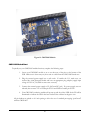
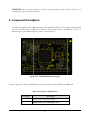
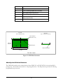
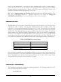
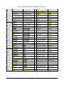
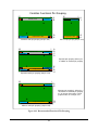
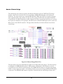
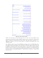
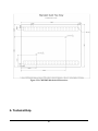
ALTERA® EP4CE115/55/30 MODULE
CMCS1003 Quick Start Guide
801 East Plano Parkway, Suite 158
Plano, TX 75074
www.dallaslogic.com
Version 1.0- May 2012
©2010 by Dallas Logic Corporation. All rights reserved.
1
This document is the property of, and is maintained by Dallas Logic Corporation. Please submit any
questions, corrections, or suggestions to [email protected]. Dallas Logic Corporation shall under
no circumstances be liable for damages or related expenses resulting from the use of this document. Your
use of this information indicates your understanding of, and agreement with the disclaimer located on the
last page of this document.
Table of Revisions
Revision
Author
1.0
JT
Date
Description
05-29-2012 Released
2
Table of Contents
1.
Introduction ............................................................................... 5
CMCS1003 Quick Start ................................................................................................ 6
2.
Component Descriptions ......................................................... 7
Altera Cyclone IV Device Resources ........................................................................... 8
CMCS1003 Devices ..................................................................................................... 9
EPCS64 serial flash ............................................................................................................... 9
64M X 16 DDR-2 Memory .................................................................................................... 10
USB Interface ....................................................................................................................... 10
JTAG and ASMI Programming Headers ............................................................................... 10
Reset Circuit......................................................................................................................... 11
FPGA User IO Bank Voltage ................................................................................................ 11
Indicator LED ....................................................................................................................... 11
3.
Setup and Programming ........................................................ 11
CMCS1003 Module Setup ......................................................................................... 11
Altera Software and FPGA Programmer............................................................................... 12
CMCS1003 FPGA Programming Instructions ....................................................................... 12
Cyclone IV Pin Voltage Sensitivity (over-shoot and under-shoot) ......................................... 13
5V Interfacing With Cyclone IV ............................................................................................. 13
CMCS1003 Module Power ................................................................................................... 14
Cardstac Support – CMCS1003 Design ............................................................................... 14
Altera Reference Documents ............................................................................................... 15
4.
CMCS1003 Design Information ............................................. 15
Pin Function Mapping ................................................................................................ 15
Quartus II Starter Design ........................................................................................... 18
Quartus II Tutorial Instructions.............................................................................................. 20
CMCS1003 Design Schematic ............................................................................................. 20
5.
Mechanical Dimensions ......................................................... 20
6.
Technical Help ........................................................................ 21
3
CMCS1003 Module Technical Help ...................................................................................... 22
Warranty Information ............................................................................................................ 23
7.
Disclaimer ................................................................................ 23
List of Figures
Figure 1-1 CMCS1003 Module ............................................................................. 6
Figure 2-2-1 CMCS1003 Silkscreen Legend ........................................................ 7
Figure 2-2-2 PCB Pin Orientation ......................................................................... 8
Figure 4-4-1 Recommended Functional Pin Grouping ........................................ 17
Figure 4-4-2 Starter Design Block View .............................................................. 18
Figure 4-4-3 Nios II block symbol ....................................................................... 19
Figure 5-5-1 CMCS1003 Mechanical Dimensions .............................................. 21
List of Tables
Table 2-1 Designator Identification ....................................................................... 7
Table 2-2 EP4CE30/55/115 FPGA Resources ..................................................... 9
Table 2-3 Nios II Performance and Resource Utilization ...................................... 9
Table 3-1 CMCS1003 Power Input Fusing ......................................................... 14
Table 4-1 Recommended Pin Mapping (16 bit interface) .................................... 16
4
1. Introduction
The purpose of this document is to provide users of the CMCS1003 module a guide for performing
power up, programming, and general circuit and connector identification. The CMCS1003 is primarily
intended as an FPGA module (Altera EP4CE30/55/115),
/115), but also provides support circuits to enable
operation as an Altera Nios II controller. The following list identifies the primary feature set of the
CMCS1003 module:
•
•
•
•
•
•
•
•
•
•
•
Altera® EP4CE30/55/115
/115 FPGA, in –C8
C8 speed grade and 484 pin BGA package.
Separate programming ports (ASMI flash interface and JTAG interface).
Reset and voltage monitor IC which provides 400mS reset pulse.
Reset push-button switch.
109 input/output
tput pins available on stack
stack-through header.
3 discrete indicator LED (red, yellow, green).
Clock oscillator (25 MHz) TCXO
TCXO.
compatible design. Populated with stack-through connector.
EPCS64 (64Mbit) serial flash for FPGA configuration and Nios II ssoftware.
64M x 16 bit (1Gbit) DDR2 SDRAM for Nios II program execution and dynamic data storage.
USB 2.0 High speed port (FT232H).
The CMCS1003 FPGA kit has everything you need to start designing with and evaluating the powerful
features of Altera® Cyclone IVTM FPGA devices. The kit provides an Altera Byte Blaster II or USB Blaster
FPGA programmer and a 3.3V power supply. Individual CMCS1003 modules (no kit components) are
also available. Whether you want to learn about FPGA design, or have a specific design implementation
to complete, this FPGA module will jum
jump-start your own Cyclone IVTM design efforts. Your CMCS1003
kit includes the following items:
CMCS1003 module
Wall mount type 3.3VDC/2A switching power supply ((US
US or Asian/European model,
depending on geographic location)
Altera® ByteBlaster II or USB Blaster FPGA programmer
5
Figure 1-1 CMCS1003 Module
CMCS1003 Quick Start
To quickly see your CMCS1003 module function, complete the following steps:
1. Locate your CMCS1003 module so as to not short any of the pins on the bottom of the
PCB. Make sure to clean away any loose wire or solder from the CMCS1003 bench area.
2. Plug the external power-supply into a wall outlet. If outside the U.S., make sure you
received the Asian/European model and have an appropriate plug adapter (supply input
voltage is 230V AC, 50/60Hz in some areas overseas).
3. Connect the external power supply to P1 (0.65 mm DC jack). If a power supply was not
ordered, then connect 3.3V to header pin P3-H1 and GND to header pin P3-H2.
4. Your CMCS1003 evaluation module will power-up and the yellow LED device D3 will be
illuminated to indicate the FPGA has been load and the software has begun to run.
All pin headers are placed on 0.1 inch spacing to allow the use of standard prototyping “perf-board”
with the CMCS1003.
6
WARNING!! Do not directly connect 5V devices to the CMCS
CMCS1003
003 IO pins. See the section on 5V
interfacing
erfacing for proper connection methods.
2. Component Descriptions
The following diagrams show a silkscreen image of the CMCS1003 PCB, as well as a pin location diagram.
You can use these images to help locate electronic devices and connector pin locations.
loc
Pin A1 is
indicated by the yellow silkscreen square (white on the actual PCB).
Figure 2-2-1 CMCS1003 Silkscreen Legend
Using the figure above and the table below the major components on the CMCS1003 are identified.
Table 2-1 Designator Identification
Designator
Description
U8
FPGA Cyclone IV EP4CE115/55/30
U2
64Mbit Serial Flash (FPGA program store)
7
U5
32Mx16 DDR2 DRAM
U9
25MHz. Oscillator
U6
FTDI FT232H High Speed USB Transceiver
P1
Altera ASMI programming Interface
P4
Altera JTAG programming Interface
P5
DC Jack, 3.3V, 2.5A Max (.65mm center pin positive,
2.8mm outer diameter)
P2
USB Mini B Connector
Top View
(from component side)
32
End View
(top or component side up)
1
Pin A1 indicator
(PCB silk-screen)
A
B
2.34 inch
59.4 mm
Mounting Hole
G
H
Bottom Side Spacer
3.44 inch
87.4 mm
Full Card, 128 pin
Figure 2-2-2 PCB Pin Orientation
Altera Cyclone IV Device Resources
The CMCS1003 module can be ordered with an Altera EP4CE115 or EP4CE30 FPGA in the 484 pin BGA
package (U5). The module comes with the –C8 speed grade device. The 484 pin device provides the following
programmable logic resources:
8
Table 2-2 EP4CE30/55/115 FPGA Resources
FPGA
EP4CE30
EP4CE55
EP4CE115
Logic Elements (approx. 50 gates per LE)
28,848
55,856
114,480
M9K RAM Blocks (9216 bits per block)
66
260
432
RAM (K bits)
594
2,340
3,888
PLLs
4
4
4
18bit x 18bit multipliers
66
154
266
Consult Altera’s Cyclone IV Device Handbook for detailed information on internal device timing and
design speed estimation. Some benchmark numbers for Altera’s Nios II processor are also shown in the
table below. These numbers are taken directly from Altera’s “Nios II Performance Benchmarks”
document (not from our own benchmarks). Note that the LE utilization for the Nios II does not include
items such as a UART or timer. Both of these devices require approximately 75 LE each.
Table 2-3 Nios II Performance and Resource Utilization
Device
Maximum
Frequency
/MIPS Nios
IIe
Maximum
Frequency
/MIPS Nios
IIf
EP3C40-C6
215 MHz/ 30
MIPS
175 MHz/194
MIPS
LE
utilization
Nios IIe
650
LE
utilization
Nios IIf
1800
LE
utilization
UART
75
CMCS1003 Devices
EPCS64 serial flash
The EPCS64 (M25P64) serial flash device (U2) is used to load the FPGA hardware configuration data.
The EPCS64 device is a 64 Mbit device and contains 67,108,864 bits of program space. The EP4CE115
FPGA requires 28.6 Mbits (non-compressed) for its configuration load, which leaves 38.5 Mbits for
9
processor software images or user data. The EP4CE30 FPGA requires 9.5 Mbits (non-compressed) for its
configuration load, which leaves 57.6 Mbits for processor software images or user data. Cyclone IV
devices support compression of FPGA configuration loads. Compression will typically provide 35% 50% reduction in space requirements of the configuration load. This can be implemented if more user
data space is required. Note that the size of the compressed FPGA load is not fixed, and will vary from
compile to compile. The EPCS64 device supports byte or buffer moves of data, and also has software
driver and interface support via Altera’s SOPC builder.
64M X 16 DDR-2 Memory
The 64M x16 DDR-2 SDRAM device (U5) is located on the top of the PCB. This device is primarily
provided for Nios II or other CPU program and data storage. For Nios II processors (32 bit instruction),
two SDRAM access are required to fetch a single instruction. This is automatically handled by Nios II
using dynamic bus sizing. The device is a Micron MT47H64M16HR-25E:H (or equivalent), which is an
DDR-2 SDRAM device. On the CMCS1003 design, the DDR-2 has a dedicated address and data bus.
To disable the SDRAM device, drive the DDR2_PWR_OFF- pin low in your FPGA design. This pin is
tied a high in the CMCS1003 reference design.
USB Interface
The CMCS1003 board provides an FTDI FT232H device to support serial communications to your
design. This device will allow terminal communications, or data transfer under program control. The
FT232H supports full or high speed operating modes and data transfer rates up to 480Mbit/s. A driver
for the FT232H can be downloaded from the FTDI website. For more information on the FT232H, visit
the manufacturer’s web page at: http://www.ftdichip.com/Products/ICs/FT232H.htm
JTAG and ASMI Programming Headers
Two separate 10 pin programming headers are provided on the CMCS1003 module. One header is for
the ASMI flash interface (P1) on the EPCS64/Cyclone IV devices, and the other is for the Cyclone IV
JTAG port (P4). Two separate programming ports allows the CMCS1003 design to support Flash reads
and writes at the same time the JTAG port is being used for operations like Altera SignalTap logic analyzer
(Quartus II feature), or in-circuit debug. The ASMI port is used to program the FPGA flash image (.pof
file)
into the EPCS64 flash device.
The JTAG port is used to program the DDRII RAM image directly into the FPGA (.sof file). Note that pins 1 of both the JTAG (P4) and ASMI (P1)
connectors are located towards the “top” of the PCB assembly (silkscreen “1” indicates pin 1 on each
connector). When plugging in the Byte Blaster II or USB Blaster programmer, the white line identifies pin
1 and the ribbon connector should be plugged in with the white line towards the “top” (towards pin 1) on
both P4 and P1. See section “CMCS1003 FPGA Programming Instructions” for more details on ASMI
and JTAG programming procedures.
10
Reset Circuit
The CMCS1003 module provides a TPS3802 voltage monitor (U4). The reset input of this device is active
low and the device reset output drives the dedicated reset pin on the Cyclone IV FPGA device. A
Quartus II setting defines this Cyclone IV FPGA pin to be either a dedicated chip wide reset or a user IO.
Even if the pin is defined as user IO, the signal can still be used to reset individual circuits within a given
design.
The TPS3802 will provide a 400mS reset pulse for the following events:
Module power up
Press of S1 push-button
3.3V power out of range
Following FPGA configuration and loading
During FPGA initialization, the conf_done (open drain) pin from the FPGA asserts the MR- (manual
reset) input pin of the TPS3802 and causes a logic reset to the FPGA. Once the FPGA has finished
loading, conf_done will float high, and reset will de-assert approximately 400ms after FPGA configuration
has finished. Note that this reset signal is driven locally to the FPGA only and is not connected to the
PCB pin header (Cardstac reset). The FPGA must drive reset on the external pin via your design.
FPGA User IO Bank Voltage
There are eight separate IO banks on the EP4CE30 / 115 Cyclone IV devices. On the CMCS1003
module, six banks are powered by 3.3V and two banks (Bank 7 & 8) are powered with 1.8V. Bank 7 & 8
provide the DDR-2 Interface and are configured for SSTL-18 Class I.
Indicator LED
The CMCS1003 module provides three general purpose LED outputs (green, yellow, red).
3. Setup and Programming
CMCS1003 Module Setup
Steps to setup and run your CMCS1003 module are:
1. Locate the PCB and module so as to not short any of the pins on the bottom of the PCB.
Make sure to clean away any loose wire or solder from the CMCS1003 bench area.
2. Connect the ByteBlaster II or USB Blaster cable to P4 (JTAG) programming header.
3. Plug the external power-supply into a wall outlet. If outside the U.S., make sure you
received the Asian/European model and have an appropriate plug adapter (supply input
voltage is 230V AC, 50/60Hz in some areas overseas).
11
4. Connect the external 3.3V power supply to P5 (0.65mm DC jack). If a power supply was
not ordered, then connect 3.3V to header pin P3-H1 and GND to header pin P3-H2.
The CMCS1003 module will run and will illuminate the yellow LED device.
Note that the CMCS1003 module can accept 3.3V input voltage via the 0.65mm DC jack (P5-center pin
positive). It can also be powered by using pin H1 (3.3V) and pin H2 (GND) of P3. Pin H2 is a ground
pin, and pin H1 is a 3.3V power pin. P3-H1 can be used to input power to the CMCS1003, or if the DC
JACK is attached to the CMCS1003, then pin H1 can provide power to external circuits. Do not connect
the DC JACK to the CMCS1003 if you have 3.3V attached to pin H1 from another power source. Note
that pins H1, G2, B31, and A32 are all 3.3V power pins. The current limit for each pin is 2 Amps. The
CMCS1003 is designed to operate at 3.14 – 3.46V (3.3V +/- 5%) and requires approximately 500 mA of
current with a minimal FPGA design. Do not exceed this voltage specification when applying external
power.
Altera Software and FPGA Programmer
Your CMCS1003 requires Altera’s Quartus II development software, and an FPGA programming device
(included in the kit). Quartus II should be installed on your PC to provide FPGA design and Nios
II/SOPC support (Nios II/SOPC install is optionall). Quartus II is used to compile your design files and
Program the Cyclone IV FPGA on the CMCS1003 module (via the FPGA programmer cable). Nios
II/SOPC installation is required only to support implementation of Nios II processor designs. Quartus II
version 11.0 SP1 for Windows requires Microsoft Windows XP or Windows 7. If using the web edition,
you will be required to request a web edition license from Altera, even though the software is free of
charge.
Web edition Quartus II provides incredible design capability and fully supports the Cyclone IV line of
FPGA devices (web edition has limited compile functionality for Stratix and higher end FPGA devices).
The web edition of Nios II/SOPC builder is a trial version and implements a “tether” limitation for Nios
II processors. This means that a Nios II processor instantiated with trial software will quit functioning if
disconnected from the Altera programmer. For learning or testing on the CMCS1003 module this is not a
serious limitation, but to implement working Nios II designs for your own products, you will have to
acquire a full Nios license.
The ByteBlaster II cable is connected to the LPT (printer) port of your Windows/Linux PC. The USB
Blaster is connected to a USB port. For detailed information on Quartus II/Blaster installation, setup, and
requirements access www.altera.com and reference their online documentation.
CMCS1003 FPGA Programming Instructions
The CMCS1003 FPGA device can be programmed at any time using the JTAG port (using a .sof file), or
by the EPCS64 serial flash device at board power up. A non-volatile flash image is loaded into the
EPCS64 device (using a .pof file) by the user via the ASMI port. The two possible methods for
programming the CMCS1003 Cyclone IV FPGA device are:
12
1. Use a .sof file and program the FPGA directly. To do this, connect the Byte-blaster to the JTAG
port. Open the Altera programmer software and be sure “JTAG” Mode is selected. Next, click
the “Auto Detect” button. Right click on the FPGA device that is listed and select “Change file”.
This will allow you to select a .sof file and assign it to the listed device. Finally, click the “Start”
button to program the FPGA device. This is a temporary load. If power is removed the FPGA
must be re-programmed.
2. Use a .pof file and permanently flash a new load into the EPCS64 device via the ASMI interface.
To do this, attach the Byte-blaster to the ASMI port. Open the Altera programmer software and
change to “Active Serial Programming” Mode. Select “Add file” and browse to your project .pof
file. Finally, make the desired programming selections (check mark) and press the “Start” button.
This will store the FPGA load in the serial flash device. Cycle power on the CMCS1003 board to
load the flash image into the FPGA device. Note that you cannot "auto-detect" on the ASMI
port. Important: when the project file was compiled, you must have selected the EPCS64 as the
target device and the mode as “Active Serial Programming”. Other selections such as “Generate
compressed bit-streams” must also be assigned at this time. These selections are found under the
“Assignments – Device” menus in Quartus II (click the “Device and Pin Options” button and
select the “Configuration” tab).
Cyclone IV Pin Voltage Sensitivity (over-shoot and under-shoot)
Cyclone IV FPGA device IO pins are sensitive to over-voltage and under-voltage conditions (under 0V
and over 3.3V). This includes over-shoot and under-shoot from un-terminated signal lines. Make sure to
include series termination where possible, and check over-shoot and under-shoot on all IO pins. Also, if
driving signals to the Cyclone IV FPGA from another FPGA device, reduce the amount of drive current
that is programmed in the driving FPGA design to a minimum. Refer to Altera application note AN-4472.0, Interfacing Cyclone III and Cyclone IV Devices with 3.3/3.0/2.5-V LVTTL/LVCMOS I/O
Systems for more information. Cyclone IV devices implement PCI clamping diodes on pins which are
not configured for device programming to protect against over-voltage conditions. For example, active
serial configuration pins ASDO and nCSO do not provide clamping diodes when used for programming
operations. Clamping diodes are connected between the signal pin, and the VCCIO rail of the board
(3.3V on the CMCS1003). Usually, series resistors can be implemented to protect device inputs (clamping
diodes) from over-current damage. The Cyclone III clamping diodes have a sink current limit of 10 mA
DC.
5V Interfacing With Cyclone IV
WARNING!! Do not directly connect 5V devices to the CMCS1003 IO pins. Read further for proper 5V
connection methods.
Cyclone IV devices do not directly support 5V VIO and therefore 5V interfacing techniques must be
implemented. All Cyclone IV devices use PCI clamping diodes on pins which are not configured for
device programming (for example, active serial configuration pins, ASDO, nCSO). Normally, series
13
resistors can be implemented to protect device inputs (clamping diodes) from over-current damage.
Cyclone IV devices, however, are very sensitive to over-voltage and under-voltage, even from conditions
like signal ringing on un-terminated lines. Because of the sensitive nature of Cyclone IV devices, a 5V
translator IC should be utilized when interfacing to 5V devices.
Make sure you properly translate any 5V circuits that are connected to the CMCS1003 module to 3.3V
levels using an appropriate translator IC. Improper connection of 5V circuits can damage the
CMCS1003 Cyclone IV FPGA or the external components that you are interfacing to.
CMCS1003 Module Power
The CMCS1003 3.3V power plane is sourced from pin groups H1/G2 and B31/A32. Each pin on the
CMCS1003 is rated at 2 Amps. Each pin group (H1/G2 and B31/A32) is fused at 4 Amp. The
CMCS1003 3.3V power rail should operate in the range of 3.14V - 3.46V. Pin group H1/G32 is protected
with fuse F3, pin group B31/A32 is protected with fuse F1, and the 3.3V DC jack input P1 is protected by
fuse F2 (2.5A). The CMCS1003 kit power supply (via P5 DC jack) can be used to supply 3.3V power to
circuits external to the CMCS1003 module (via pin header pins). If the opposite scenario is implemented,
and power is to be supplied to the CMCS1003 module via the header pins (3.3V), do not plug the external
power supply into the DC jack (power applied by both header pins and the DC jack). Make sure you do
not exceed the fuse limitation of the CMCS1003 module when connecting and powering external devices.
Table 3-1 CMCS1003 Power Input Fusing
3.3V Input
Current Limit
DC Jack (P1)
2.5 A
Pin Group H1/G2
4A
Pin Group B31/A32
4A
Even though two separate pin groups are implemented which uses two fuses, both of these pin groups are
connected to the same 3.3V rail on the CMCS1003 (to support installation of two separate Cardstac half
cards). This implies that the effective current limit on all four pins (H1, G2, B31, A32) is 8 Amps. These
four pins MUST be connected to the same external 3.3V supply.
Cardstac Support – CMCS1003 Design
The CMCS1003 was designed to support the Cardstac specification. The following header pins on P3
have 1.8K Ohm pull-up resistors attached:
Pin H3 (RST-), R9
14
Pin A2 (1I2C_SCL), R11
Pin A3 (1I2C_SDA), R10
Pin A5 (IRQ4B-), R7
Pin H28 (IRQ0A-), R5
Pin H30 (0I2C_SDA), R3
Pin H31 (0I2C_SCL), R1
These resistors can be removed if pull-ups are not required. For more information on Cardstac, download
the specification located at www.dallaslogic.com.
Altera Reference Documents
This User Manual is a guide to the CMCS1003 reference design as well as a guide for basic Quartus II
programming operations. It is not intended to replace the standard set of Altera documentation that is
necessary for detailed design of Cyclone IV FPGA systems. All of Altera’s documentation is available
online at www.altera.com.
4. CMCS1003 Design Information
Pin Function Mapping
For additional information on CMCS1003 pin function mapping, refer to the Cardstac specification
available for download from www.dallaslogic.com. Because the CMCS1003 is an FPGA based module, all
signal pins can be programmed as IO (both input and output). The Quartus II starter design defines
FPGA pin locations. The CMCS1003 module is a Cardstac standard card (128 pins on two stack-through
pin headers). The stack-through pin headers provides four 3.3V power pins, six GND pins, and 110 signal
pins. There are also 2 pin locations that are reserved for 12V power input (not implemented on
CMCS1003). The following two diagrams show recommended pin function mapping for the
CMCS1003M module. Note that the gray highlighted pins indicate synchronous FIFO bus functions.
Yellow highlighted pins clock, reset, and power functions.
15
Table 4-1 Recommended Pin Mapping (16 bit interface)
PIN
ROW A
ROW B
ROW G
ROW H
1
GND
1SPI_CLK
VAUX0 / +12V
+3.3V
2
1I2C_SCL
1SPI_MOSI/5TX
+3.3V
GND
3
1I2C_SDA
1SPI_MISO/5RX
CS0-
RST-
4
IRQ5B- / 4CTS
1SPI_SSN3-/4TX
CS1-
ADD0
5
IRQ4B- / 3CTS
1SPI_SSN2-/3TX
CS2-
ADD1
6
S-CLK4
1SPI_SSN1-/4RTS
CS3-
ADD2
7
GND
1SPI_SSN0-/3RTS
CS4-
CLK0
8
S-CLK3
IRQ7B- / 4RX
DATA0
GND
9
S-DP1
IRQ6B- / 3RX
DATA1
WRITE-
10
S-DP0
S-D15 / IO7B
DATA2
ADD3
11
S-STAT9
S-D14 / IO6B
DATA3
ADD4
12
S-SYNC-
S-D13 / IO5B
DATA4
ADD5
13
GND
S-D12 / IO4B
DATA5
READ-
14
S-CLK2
S-D11 / IO3B
DATA6
GND
15
S-STAT8
S-D10 / IO2B
DATA7
ADD6
16
S-STAT7
S-D9 / IO1B
DATA8 / IO0A
ADD7
17
S-STAT6
S-D8 / IO0B
DATA9 / IO1A
ADD8
18
S-CLK1
S-D7
DATA10 / IO2A
ADD9
19
GND
S-D6
DATA11 / IO3A
ADD10
20
S-READ-
S-D5
DATA12 / IO4A
GND
21
S-STAT5
S-D4
DATA13 / IO5A
ADD11
22
S-STAT4
S-D3
DATA14 / IO6A
ADD12
23
S-STAT3
S-D2
DATA15 / IO7A
ADD13
24
S-WRITE-
S-D1
IRQ2A- / 0RX
ADD14 /WAIT-
25
GND
S-D0
IRQ3A- / 1RX
ADD15 /BE0-
26
CLK1 (S-CLK0)
S-SEL4
0SPI_SSN0-/0RTS
GND
27
S-STAT2
S-SEL3
0SPI_SSN1-/1RTS
ADD16 /BE1-
28
S-STAT1
S-SEL2
0SPI_SSN2-/0TX
IRQ0A- /0CTS
29
S-STAT0
S-SEL1
0SPI_SSN3-/1TX
IRQ1A- /1CTS
30
RST-
S-SEL0
0SPI_MISO/2RX
0I2C_SDA
31
GND
+3.3V
0SPI_MOSI/2TX
0I2C_SCL
32
+3.3V
VAUX0 / +12V
0SPI_CLK
GND
16
Cardstac Functional Pin Grouping
32
1
FIFO bus-16 bit
V+
Serial bus
Serial bus
Peripheral bus-16 bit
V+
A
B
G
H
Standard 16 bit pin grouping (128 pin card)
32
FIFO bus-32 bit
1
Serial bus
Peripheral bus-8 bit
V+
A
B
G
H
Half card pin grouping (60 pin card)
1
V+
Serial bus
15
Serial bus
V+
A
B
C
D
Expanded pin grouping defines pins
in addition to standard pin grouping.
V+
Serial bus
Serial bus
Peripheral bus-32 bit
V+
Expanded 32 bit pin grouping (256 pin card)
32
E
F
G
H
1
Serial bus
V+
A
B
Alternate pin grouping is defined as a
substitution for standard pin grouping.
It is for designs that require a 32 bit
peripheral bus on a 128 pin card.
Serial bus
V+
Peripheral bus-32 bit
G
H
Alternate 32 bit pin grouping (128 pin card)
Figure 4-4-1 Recommended Functional Pin Grouping
17
Quartus II Starter Design
The starter design was created to provide a board level functional test for the CMCS1003. The design
includes a Nios II soft controller, PLL, IO Control Block, DDR-II RAM interface and Cardstac pin
definitions. The design exercises the onboard DDR-II RAM, LEDS and UART by executing a program
from onboard memory. The Cardstac I/O pins are driven using the NIOS II soft controller and the IO
Control Blocks, the NIOS II firmware routine is designed for using a special test board that cross connects
the IO pins for verification of IO operation. The PLL uses the onboard 25 MHz input clock to create a 20
MHz clock for the NIOS II controller. The figure below identifies the functional blocks located in the
starter design.
NIOS II
DDR2
UART Pins
IO Control Blocks
Cardstac Pins
Figure 4-4-2 Starter Design Block View
The figure below shows the NIOS II block symbol for the CMCS1003 starter design. The Nios II design
is comprised of a DDR-II RAM interface, UART interface, LED interface, PIO Interfaces to the IO
Control Blocks and an EPCS controller interface. The DDR-II RAM interface was designed using SOPC
builder’s custom component wizard. All remaining interfaces were created using predefined SOPC builder
components. The DDR-II RAM interface component is included with the starter design reference files.
18
Figure 4-4-3 Nios II block symbol
NOTE: The starter design was created using Quartus II ver. 11.0 SP1. Some user modification of the
starter design may be required to support compilation under later versions of Quartus II. Quartus II "web
edition" is available for download from the Altera website. This starter design is provided "as is".
Modification or support of the Nios II starter design is not included in the purchase price of the
CMCS1003 module.
Your CMCS1003 module comes with the CMCS1003 starter design stored in the EPCS64 flash device.
After applying power to the module, the Yellow LED device will illuminate, and the module IO pins will
be toggled by a CMCS1003 NIOS-II soft processor firmware. All of the FPGA IO pins are defined
making it an easy job to connect nets of your own logic circuits to external pins. To modify and add to the
design, you will need to obtain the starter design Quartus II project archive (.qar file). This file is available
upon request from us at [email protected]. This file should be “de-archived” to a project folder
located on your PC.
19
For the CMCS1003 starter design, Altera “mega-function” blocks were instantiated for logic circuit
functionality, and then graphical representations of those blocks (.bdf files) were “stitched” together using
Altera’s graphic schematic editor. This creates the top-level graphical “.bdf” design file (hierarchical
design) from which, it is very easy to analyze and interpret design intent. Quartus II supports VHDL, and
Verilog HDLs. The graphical representations of these HDL blocks can also be added to the top-level
design file.
Quartus II Tutorial Instructions
After installation of the Quartus II web edition toolset, it is highly recommended that you go through
Altera’s Quartus II tutorial. The tutorial will help you to become comfortable with the QII development
environment.
Launching QII:
•
Double click the Quartus II shortcut (icon) found on the desktop of your computer (or navigate
to the Altera folder and double click the Quartus II program icon).
•
Allow the computer to search the Altera site for updates. This will ensure that you have the latest
copy of web edition.
•
Under the Help menu on the top toolbar, select getting started tutorial.
•
At the top of the tutorial window push the Next button this will take you through tutorial basics
and into the design sections.
Once you have completed the tutorial sections you will be ready to explore the CMCS1003 design.
The CMCS1003 design project can be opened from the “CMCS1003.qpf” file located in the CMCS1003
project directory. The CMCS1003 design top level module (top.bdf) was created using Altera’s schematic
editor. The schematic allows the user to create graphical block representations for sub-modules. These
sub-modules can then be stitched together using “wires” for connectivity.
CMCS1003 Design Schematic
CMCS1003 schematic pages should be referenced for details on circuit design or when connecting devices
to the supplied pin-headers. The schematic (.pdf file) pages are available upon request. Please send us an
email at [email protected] to receive a copy of the schematic.
5. Mechanical Dimensions
The mechanical dimensions for the CMCS1003 module are shown in the diagram below.
20
Figure 5-5-1 CMCS1003 Mechanical Dimensions
6. Technical Help
21
CMCS1003 Module Technical Help
Being an “internet-centric” company, Dallas Logic provides manned 24hr email and web forum support.
The best way to obtain help with problems is to post questions to our online support forum. We are
prompt about replying, and there is also a good chance you will find your question has already been
answered online in the forum.
If you prefer email support, we can be reached at
[email protected]. We will generally reply within 24hrs of receiving an inquiry or request for help
with problems that are related to the operation of your CMCS1003 module. Before contacting us with
inquiries, please make sure you have:
1. Verified fuses F1, F2, and F3 (located on the top side of the PCB) and checked the 3.3V input level at
header pin P3-H1.
2. Removed any test circuits from connection to the CMCS1003 PCB and restored it to its original design
state (remove any modifications and restore original circuits).
3. Re-programmed and tested your CMCS1003 module with the original reference design file.
For questions related specifically to Altera software tools or FPGA devices, we can sometimes be of
assistance, but will generally refer you to the Altera online knowledge base or online support web pages.
22
Warranty Information
Your un-modified CMCS1003 assembly is guaranteed to be free of defects in material and workmanship for a period of
ninety days from the date of purchase. If your CMCS1003 module stops working during the ninety day period, and is in its
original, un-modified state, first contact us at [email protected]. If the problem cannot be resolved, you must return
the PCB assembly and power supply, postage prepaid to Dallas Logic Corporation. All repairs and return ship will be made
within 10 days of receipt of package. During the warranty period, Dallas Logic will, at its option, repair, replace, or refund
the purchase price. Products that have been damaged or modified from their original design state are not covered by
warranty. No warranty is implied with respect to the software or firmware files.
7. Disclaimer
Information in this document concerning the devices, applications, or technology described is intended to suggest possible
uses and may be superseded. Customers are advised to obtain the latest version of device specifications before relying on
any published information. Dallas Logic Corporation DOES NOT ASSUME LIABILITY FOR OR PROVIDE A
REPRESENTATION OF ACCURACY OF THE INFORMATION, DATA FILES, DEVICES, OR TECHNOLOGY described in
this document. Dallas Logic Corp. also does not assume liability for intellectual property infringement related in any manner
to use of information, devices, or technology described herein or otherwise. Dallas Logic Corp. makes no warranty of
merchantability or fitness for any purpose and does not assume liability for damages incurred to property due to the use of
this product or implementation of information or procedures listed in this document. Use of information or technology as
critical components of life support systems is not authorized. No licenses are conveyed, implicitly or otherwise, by this
document under any intellectual property rights.
23