1
an
on
TM501, TM502, TM503
RIGID DISK DRIVES
"
.
PRODUCT SPECIFICATION AND USER'S MANUAL
TM501, TM502, TM503
345 TRACKS PER INCH
PRODUCT SPECIFICATION AND USER'S MANUAL
!
I an i:fii'n CORPORATION
20320 PRAIRIE STREET
CHATSWORTH, CALIFORNIA 91311
© COPYRIGHT 1983 TANDON CORPORATION
CONTENTS
Section
Number
Title
SECTION 1
GENERAL DESCRIPTION
Page
Number
1.4
1.5
Introduction............................ ......................................................
Scope Of The Document...................................................................
Purpose Of The Drive.......... ................................. . ...... ...... ..............
Major Features...............................................................................
Microprocessor ControL ............................................... , . . . . . .. . . ... . . . .
Daisy Chain Capability ...... ....... ..................... , .. . . . . . . . .. ... ... . . ... . .. . . . . ..
Industry Standard Interface Compatibility..... ....................................
Activity Indicator.. . . . . .. . .... . . . . . . . . .. . . . .. . .. .. .. . . .. . .. .. . . .. . . . .. . . . . . . .. . . . . .. . . . . ..
Air Filtration............................. ....... ............. ........................... ..
Functional Description. ......................................... ....... ..... ............. ..
Physical Description.......................... ............. .......................... ... ....
SECTION 2
PRODUCT SPECIFICATIONS
2. 1
2.2
2.3
2.4
Introduction..................................................................................
Mechanical Specifications................................................ .................
Electrical and Operational Specifications.......................... ........ ...... ......
Reliability Specifications............................. ........................ ....... .......
Environmental Specifications............. .. .. ...... ..... . ................................
SECTION 3
OPERATION
1.1
1.2
1.3
3.1
3.2
3.3
3.4
3.5
3.6
3.7
Introduction..... ............. ..... .................................. ....... ....... ...........
Unpacking The Drive....... .. .......... ... . ................................................
Preinstallation Checkout...... ..... .................. .....................................
Mounting The Drive............................. ........ ....... ..... .......................
Dust Cover.......................... . ....... ...... . ....................... ............... ..
Free Air Flow..............................................................................
Confined Environment.. ..... .. ..... ...... .......................... ....................
Interface Connectors.................................... ..... . .............................
J1/P1 Connector.........................................................................
J2/P2 Connector ........ ...... ...... . ...... ... .... ....... ... .......... ....... ,'...........
J3/P3 Connector ................. ............................ . ..... ......... :............
Frame Ground Connector. ....................................... ......................
Interface Line Descriptions................................. ..... ..........................
Input Control Signals....... .. ................................ ...... .. ...... .............
Output Control Signals ............... ...................................................
Data Transfer Signals ......... ............................. ............ ..................
Drive Address and Option Selection .... .................................................
Shipping Pack and Handling ............................................ ..................
1-1
1-1
1-1
1-1
1-1
1-1
1-1
1-2
1-2
1-2
1-2
2-1
2-1
2-1
2-1
2-1
3-1
3-1
3-1
3-1
3-3
3-3
3-3
3-3
3-3
3-3
3-6
3-6
3-6
3-6
3-12
3-13
3-14
3-14
ILLUSTRATIONS
FIGURES
Figure
Number
1-1
2-1
2-2
3-1
3-2
3-3
3-4
3-5
3-6
3-7
3-8
3-9
3-10
3-11
3-12
3-13
3-14
Page
Number
Title
Disk Drive............................... ........ .... ..... .. ...................................
Disk Drive Outline Drawing.................... .................................... .......
Typical Starting Currents................................... .... ........................ ...
Four Pack Shipping Container............... ............................................
Jl Edge Connector Dimensions....................... ....... ...... ........ ............ ..
J2 Edge Connector Dimensions......... .............................................. ...
J3 Power Connector........................................................... .............
Radial Configuration............................. ..........................................
Daisy Chain Control Lines. ........ .......................................................
Control Signal/Driver Receiver
Circuit Combination............... ..... ........................................ ............
Step Mode Timing........................................ .. .............. ............. .. ....
Buffered Seek Step Pulses ........ . ........................................................
Data Transfer Line Driver Receiver .....................................................
Recommended Shipping Pack Design,
Configuration 1........................ ......................................................
Recommended Shipping Pack Design,
Configuration 2 ..............................................................................
Recommended Shipping Pack Design,
Configuration 3............................... ............................. . .................
Load Graph...................................................................................
1-2
2-2
2-5
3-2
3-4
3-4
3-4
3-7
3-8
3-9
3-11
3-11
3-13
3-16
3-18
3-19
3-21
TABLES
Table
Number
2-1
2-2
2-3
3-1
3-2
3-3
Page
Number
Title
Electrical and Operational Specifications.................................. .......... ..
Reliability Specifications................ ............... ......................... ...........
Environmental Specifications.................. ...........................................
Drive Interface Signals and Pin Assignments ...............................,...........
Head Select Lines ................................................................ '............
Option Programming Guide ............ ............... ...................................
ii
2-3
2-6
2-7
3-5
3-10
3-15
l
SECTION 1
GENERAL DESCRIPTION
INTRODUCTION
1. 3
This manual provides useful information to assist
the customer when incorporating the Tandon rigid
disk drive into a system.
MICROPROCESSOR CONTROL
MAJOR FEATURES
The TMSOO series of drives feature an onboard
microprocessor. The microprocessor provides five
major functions:
Tandon Corporation's TMSOO series of drives are
full feature, S-1I4-inch, rigid disk drives. They are
compact data storage devices that contain one or
more 130-millimeter plated aluminum platters
within a sealed housing.
1. Self-calibration on power-up.
2. Buffered seek timing for improved access
times.
The TMSOO series includes Model Numbers
TMSOl, TMS02, and TMS03, which have one,
two, and three recording platters, and use two,
four, and six recording heads, respectively.
3. Improved positioning with reduced
hysteresis.
4. Write current switching for optimal recording quality.
1.1
SCOPE OF THE DOCUMENT
S. Power and track fault detection.
Section 1 of this manual contains a general
description of the disk drives. Section 2 contains
the product specifications. Section 3 provides information on operation of the drives.
1.2
DAISY CHAIN CAPABILITY
The drive provides the address selection and gating
functions necessary to daisy chain a maximum of
four units at the user's option. The last drive on
the daisy chain terminates the interface. The terminations are accomplished by a resistor array
plugged into a DIP socket.
PURPOSE OF THE DRIVE
The S-1I4-inch disk drive is a rotating disk
memory device designed for random access data
storage and retrieval. Typical applications include
word processing systems, entry level
microprocessor systems, intelligent calculators,
program storage, small business computer
systems, and any application in which low cost,
random access data storage is required.
INDUSTRY STANDARD IN,TERFACE
COMPATIBILITY
The drive is compatible with controllers that use
an industry standard interface.
1-1
ACTIVITY INDICATOR
2. An index sensor, which consists of a
magnetic pick-up and index hole positioned to provide an analog signal when an index hole is detected.
The activity indicator is located on the front panel
of the drive. It is automatically illuminated when
the drive is selected.
1.5
PHYSICAL DESCRIPTION
AIR FILTRATION
The TM500 drive is shown in Figure 1-1. The
drives contain 130 millimeter storage media that
rotate at 3600 RPM, using a direct drive, brushless
D. C. motor. The recording is accomplished by
noncontact standard recording heads that are
moved by a precision split band positioning device
and stepper motor.
A self-contained, recirculating air filtration system
supplies clean air through a 0.3-micron filter. A
secondary absolute filter is provided to allow
pressure equalization with the ambient atmosphere without contamination. The entire
head-disk-actuator compartment is maintained at
a slightly positive pressure to further ensure an
ultraclean environment.
1.4
FUNCTIONAL DESCRIPTION
The drive is fully self-contained and requires no
operator intervention during normal operation.
During the power-up sequence, the spindle motor
reaches 3600 RPM, and the positioning
mechanism recalibrates the recording heads back
to Track O. At this time, a Ready signal on the interface indicates the drive is ready for operation.
The head is postioned over the desired track by
means of a four-phase stepper motor/band
assembly and its associated electronics. This positioner uses a one-step rotation to cause a one-track
radial movement. Subsequently, the recording
heads can be positioned over the desired cylinders,
and the data can be read or written from the appropriate track by selecting the desired head.
FIGURE 1·1
DISK DRIVE
The Head Disk Assembly is enclosed in a sealed
cast aluminum housing, which includes an air
filtration system to ensure a contamination-free
environment. The housing is shock mounted to a
metal frame that has the front panel attached, and
threaded holes on the sides and bottom for mounting the drive onto a chassis.
Typically, the drive uses MFM write and read data
recording methods. Data recovery electronics include a low-level read amplifier, differentiator, a
zero-crossover detector, and digitizing Circuits. No
data decoding feature is provided on the drives.
The drive has the following sensor systems:
In addition, the drive includes the read/write control electronics, the servo spindle control electronics, an index sensor, a brake assembly, and a
front panel indicator.
1. An optical Track 0 switch senses when the
Head/Carriage Assembly is positioned at
Track O.
1-2
SECTION 2
PRODUCT SPECIFICATIONS
INTRODUCTION
This section contains the mechanical, electrical and operational, reliability, and environmental
specifications for the TM501, TM502, and TM503 disk drives.
2.1
MECHANICAL SPECIFICATIONS
The mechanical and physical dimensions are contained in Figure 2-1.
2.2
ELECTRICAL AND OPERATIONAL SPECIFICATIONS
The electrical and operational specifications are contained in Table 2-1. Typical starting current requirements at nominal voltage are contained in Figure 2-2.
2.3
RELIABILITY SPECIFICATIONS
The reliability specifications are contained in Table 2-2.
2.4
ENVIRONMENTAL SPECIFICATIONS
The environmental specifications are contained in Table 2-3 .
Ia n
aD n
17904-3·001
CORPORATION. CHATSWORTH, CALIFORNIA 91311
2-1
REV. A
I
O.OS ± 0.01 in.
(1.S ± 0.3 mm)
jfoo.-------
8.00 in. maximum
(203.2 mm)
-------1'1
I
SIDE VIEW
3.38 ± 0.01 in.
85.9 ± 0.3 mm)
3.25 ± 0.01 in.
(82.6 ± 0.3 mm)
l_LJ----.-.I
J l,.,.,m.
. , . • •01 ;.
(4.8 ± 0.3 mm)
(47.5:1: 0.5 mml
3.12 ± 0.02 in.
(79.2 ± 0.5 mm)
TAPPED MOUNTING HOLES FOUR
ON BOTTOM. TWO ON EACH SIDE
6-32 UNC X .31 tn. a 9 mml DeEP 8
PLACES.
II
5.75 ± .02 in.
(146.1 ± 0.3 mm)
5.88 ± 0.01 in.
(149.4 ± 0.3 mm)
BOTTOM VIEW
5.50 ± .02 in.
(139.7±0.5 mm)
0.06 ± 0.01 in.
(1.8 ± 0.3 mm)
Note: Weight is 3.0 kilograms, 6.5 pounds maximum
/
FIGURE 2·1
DISK DRIVE OUTLINE DRAWING
Ia n
aD n
179043·001
CORPORATION. CHATSWORTH, CALIFORNIA 91311
2-2
REV. A
TABLE 2·1
ELECTRICAL AND OPERATIONAL SPECIFICATIONS
Media
Lubricated, 130 millimeter, plated
aluminum disk
Tracks Per Inch
345 TPI
Spacing, Track to Track
2.9 milinches
Number of Cylinders
306 cylinders
Number of Tracks
TM501
612 tracks
TM502
1224 tracks
TM503
1836 tracks
Disk Speed
3600 RPM ± 1 percent
Average Latency
8.33 milliseconds
Start Time
15 seconds maximum
Stop Time
15 seconds maximum
Seek Time
3 milliseconds track to track
Head Settling Time
15 milliseconds, last track accessed
Average Access Time,
Including Head Settling Time,
3 Millisecond Step Rate
321 milliseconds
Average Access Time
Using Buffered Seek,
Including Head Settling Time
85 milliseconds
Transfer Rate
5 megabits per second
Ia n
aD n
...
179043·001
CORPORATION. CHATSWORTH, CALIFORNIA 91311
2-3
REV. A
TABLE 2·1 (CONTINUED)
ELECTRICAL AND OPERATIONAL SPECIFICATIONS
Maximum Flux Reversal Density
9090 FRPI
Unformatted Capacity Per Drive
TM501
6.38 megabytes
TM502
12.76 megabytes
TM503
19.14 megabytes
Unformatted Capacity Per Surface
3.19 megabytes
Unformatted Capacity Per Track
10.4 kilobytes
POWER REQUIREMENTS
+ 12 volts D. C. ± 10 percent, 1.5 amperes typical, 5 amperes maximum during motor start-up, not to
exceed 12 seconds, 2 amperes maximum running, with no more than 50 millivolts Periodic and Random
Deviation (PARD).
+ 5 volts D. C. ± 5 percent, 0.8 amperes typical, 1.2 amperes maximum running, with no more than 50
millivolts PARD.
There are no restrictions in sequencing power supplies on or off.
"
Ia n
aD n
179043·001
CORPORATION. CHATSWORTH, CALIFORNIA 91311
2-4
REV. A
>
>
N
ID
~
+
~
~
('I)
~
N
~
~
~
0
~
Ol
$
0
Z
II)
,....
co
0
()
W
~
Z
c;>
z
a:::
::J
I-
a:::
W
lll)
LL
<
w
::2:
~
i=
------~~------~o
N
o
FIGURE 2·2
TYPICAL STARTING CURRENTS
lanCien
119043"001
CORPORATiON. CHATSWORTH, CALIfORNIA !lla'ii
2-5
REV. A
TABLE 2·2
RELIABILTY SPECIFICATIONS
SOFT AND HARD READ ERROR RATES, EXCLUSIVE OF MEDIA DEFECTS
For data that has been verified previously as error free, and when used in conjunction with a data
separator and phase lock loop of good design, the10recoverable (soft) read error rate for any subsequent
read operation shall not exceed one error in 1 X 10 bits transferred. A recoverable read error is an error
that may be corrected within five attempts to reread the data.
•
12
•
The nonrecoverable (hard) read error rates shall not exceed one error III 1 X 10 bIts transferred. A
nonrecoverable read error is an error that may not be corrected within five attempts to reread data, providing that the writing of the data previously has been verified as correct. The seek error rate is not to
exceed one error in 1 X 10 6 seeks.
MEDIA DEFECTS
Any defects on the media surface will be identified on a defect map provided with each drive. This
defect map will indicate the head number, track number, and number of bytes from index for each
defect. Each defect shall be no longer than 16 bits. Cylinders 000 and DOl are guaranteed error free.
The map is offered as a guide only. The number of defects and their location can change due to
customer system variations such as data separators.
Mean Time Between Failures
11,000 power on hours
Mean Time To Repair
30 minutes
Component Design Life
5 years
Preventative Maintenance
Not required
Ia n
aD'n
179043·001
CORPORATION. CHATSWORTH, CALIFORNIA 91311
2-6
REV. A
TABLE 2·3
ENVIRONMENTAL SPECIFICATIONS
Ambient Temperature
Operating
4°C to 50°C, 39°F to 122°F
Nonoperating
-40°C to 60°C, _40°F to 1400p
Temperature Gradient
Operating
10°C per hour, 18°F per hour
Nonoperating
Below that causing condensation
8-to-80 percent, noncondensing
Relative Humidity
Relative Humidity Gradient
Operating
20 percent per hour
Nonoperating
Below that causing condensation
2(ilC, 78.8°F, without condensation
Maximum Wet Bulb Temperature
Elevation
Operating
Density Altitude: -457 to 2,972 meters,
-1,500 to 9,750 feet
Nonoperating
Sea level to 3,650 meters,
Sea level to 12,000 feet
!
Ia n
aD n
179043·001
CORPORATION. CHATSWORTH, CALIFORNIA 91311
2-7
REV. A
SECTION 3
OPERATION
INTRODUCTION
sure to use prior steps in reverse order, and ensure
the foam stiffeners are in the proper location, with
the cardboard dividers properly in place between
the drives (see Figure 3-1).
This section contains information pertinent to the
handling, inspection, installation, and operation
of the TM500 series of drives.
3.2
3. 1
UNPACKING THE DRIVE
PREINSTALLATION
CHECKOUT
Before applying power to the drive, inspect for the
following:
Each drive is shipped in a protective container
which, when bulk packaged, minimizes the
possibility of damage during shipment.
1. Ensure the front panel is secure.
Visually examine the shipping container for possible damage. Notify the carrier immediately if any
damage is found.
2. Ensure the circuit board is secure.
3. Ensure the connectors are firmly seated.
The following procedure is recommended for unpacking the drive .
4. Ensure there is no debris or foreign
material between the frame and the
head!disk casting.
1. Place the shipping container on a flat work
surface.
5. Ensure the head! disk housing can move
freely on the shock mounts of the frame.
2. Cut the tape on the shipping container.
6. Ensure the termination resistor pack and
jumper blocks are firmly seated and in the
correct configuration.
3. Remove the foam lid and pads from the
shipping container.
4. Remove the inner container.
MOUNTING THE DRIVE
5. Remove the drive from the inner container.
3.3
6. Place the drive on a foam lined surface.
The drive can be mounted in any vertical or
horizontal plane. Eight 6-32 tapped holes are provided for mounting: two on eaclJ. side and four on
the bottom of the frame (see Figure 2-1, page 2-2).
The drive is manufactured with some critical internal alignments that must be maintained. Hence, it
is important the mounting hardware does not introduce significant stress on the drive.
CAUTION
Do not manually rotate the stepper
motor or spindle motor. Damage
to the heads and disk may result.
NOTE
The inside chamber of the drive is a
sealed compartment that must not
be opened.
Any mounting scheme in which the drive is part of
the structural integrity of the enclosure is not permitted. Mounting schemes should allow for adjustable brackets or incorporate resilient members
to accommodate tolerances.
When returning the drive to the service center, be
3-1
DIVIDER -----(4) DRIVES
INNER
CONTAINER
FOAM
FOAM
FOAM-......
,
' - - - - SHIPPING CONTAINER
FIGURE 3·1
FOUR PACK SHIPPING CONTAINER
3-2
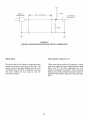
DUST COVER
data signals (see Figure 3-3). 13 provides for D.C.
power (see Figure 3-4).
The design of an enclosure should incorporate a
means to prevent contamination from loose items,
e.g., dust, lint, and paper chad since the drive does
not have a dust cover.
Table 3-1 contains interface lines. The interface
description of the connectors, and the location of
each, is contained in this section.
J1/P1 CONNECTOR
FREE AI R FLOW
Connection to 11 is through a thirty-four-pin circuit board connector. Figure 3-2 contains the
dimensions of this connector. The pins are
numbered 1 through 34. The even pins are located
on the component side of the circuit board. Pin 2
is located on the end of the circuit board connector closest to the D. C. power connector 13IP3,
and is labeled. A key slot is provided between Pins
4 and 6. The recommended mating connector for
PI is 3M ribbon connector PIN 3463-0001,
without ears.
When the drive is mounted so the components
have access to the free flow of air, normal convection cooling allows operation over the specified
temperature range (see Table 2-3, page 2-7).
CONFINED ENVIRONMENT
When the drive is mounted in a confined environment, air flow must be provided to maintain
specified air temperatures in the vicinity of the
motors and the circuit boards.
3.4
J2/P2 CONNECTOR
Connection to 12 is through a 20-pin circuit board
edge connector. Figure 3-3 contains the dimensions of this connector. The pins are numbered 1
through 20. The even pins are located on the component side of the circuit board. The recommended mating connector for P2 is 3M ribbon connector PIN 3461-0001, without ears. A key slot is provided between Pins 4 and 6.
INTERFACE CONNECTORS
The electrical interface between the drive and the
host system is via three connectors. 11 provides
control signals for the drive (see Figure 3-2). 12
provides for the radial connection of readlwrite
/
3-3
lr
2
f~
0.036 ± 0.004 in ..
(0.91 ± 0.1 mm)
4
f
- -0.450
- in. (11.4 mm)...;.....-- --- -
0.400 ± 0.010 in.
(10.2 ± 0.25 mm)
i
'~~~_L
II
--+-j
______
I
I
L __ _ _ _ _ _ _ _ _ _ _ _ _ _ _ _ _ _ _ _~II~I~I~/I
r
IIII
~(1.27mm)
~
0.050 in.
I
0.050 in. (1 .27 mm)
0.100 in. (2.54 mm)
...._ _ _ _ _ __ _ 1.775 ± 0.010 in. ______________---1~~
(45.1 ± 0.25 mm
BOARD THICKNESS
0.062 ± 0.007 in.
(1.59 mm ± 0.18 rnm)
FIGURE 3·2
J1 EDGE CONNECTOR DIMENSIONS
.
0.036 ± 0.004 in.1~
(0.91 ± 0.1 mm)
-.j
I
-r--~J
2
I
--~
t
0.063 in.
(1.6 mm)
20
")
BOARD THICKNESS
0.062 ± 0.007 in.
(1.59 mm ± 0.18 mm)
0.400 ± 0.010 in.
10.2 ± 0.25 mm)
t
......-
-
0.050 in. (1 .27 mm)
0.100 in. (2.54 mm)
FIGURE 3·3
J2 EDGE CONNECTOR DIMENSIONS
FIGURE 3·4
J3 POWER CONNECTOR
3-4
TABLE 3·1
DRIVE INTERFACE SIGNALS AND PIN ASSIGNMENTS
Interface
Pin Number
Connector
PI
I
34-Pin
Ribbon
Daisy
Chain
PI
P2
I
20-Pin
Ribbon
Radial
Ground
Signal Type
I/O
2
4
(1)
(3)
(5)
(7)
(9)
S
S
S
S
S
S
S
I
I
I
0
0
0
I
(15)
(17)
(19)
(21)
(23)
(25)
(27)
(29)
(31)
(33)
-
-
S
S
S
S
S
S
S
S
S
I
0
0
I
I
I
I
I
I
(2)
(4)
(6)
(8)
S
S
6
8
10
12
14
16
18
20
22
24
26
28
30
32
34
1
3
5
7
9
11
13
14
15
17
18
19
j
P2
P3
t
Radial
P3
NOTES:
1. S 2. D 3. I 4. 0 -
Signal
(11)
(13)
-
-
D
D
0
0
-
-
+ 12 volts D. C.
+ 12 volts D. C.
+ 5 volts D. C.
+ 5 volts' D. C.
~
(10)
-
(12)
-
D
D
(16)
-
(20)
1
2
3
4
Single Ended
Differential
Drive Input
Drive Output
3-5
Spare
Head Select i
Write Gate
Seek Complete
Track 0
Fault
Head Select 2°
Reserved (To 12 - 7)
Head Select t
Index
Ready
Step
Drive Select 0
Drive Select 1
Drive Select 2
Drive Select 3
Direction In
Drive Select
Spare
Reserved
Reserved (To J1-16)
Spare
Ground
+ Write Data
- Write Data
Ground
+ Read Data
- Read Data
Ground
-
-
Name of Signal
0
-
I
I
In
Return
Return
In
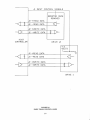
The interface may be connected in the radial or
daisy chain configuration (see Figures 3-5 and
3-6).
J3/P3 CONNECTOR
D. C. power connector 13 is a four-pin AMP
Mate-N-Lok connector, PIN 350211-1, mounted
on the solder side of the circuit board. The recommended mating connector, P3, is AMP PIN
1-480424-0, utilizing AMP pins PIN 60619-4. 13
pins are labeled on the 13 connector (see Figure
3-4). 13 cabling must be 18 AWG, minimum.
INPUT CONTROL SIGNALS
The input control signals are of two kinds: those
to be multiplexed in a mUltiple drive system and
those that do the multiplexing. The input control
signals to be multiplexed are: Reduced Write Current, Write Gate, Head Select Line 2°, Head Select
2
Line i, Head Select Line 2 , Step, and Direction
In. The multiplexing signal is Drive Select 0, Drive
Select 1, Drive Select 2 or Drive Select 3.
FRAME GROUND CONNECTOR
The frame ground connector is Faston AMP PIN
61761-2. The recommended mating connector is
AMP PIN 62187-1. To realize error rates (see
Table 2-2), it must be connected directly to the
centrally located system ground via an 18 AWG,
minimum, cable.
3.5
The input signals have the following electrical
specifications, as measured at the drive. Figure 3-7
illustrates the recommended circuit.
INTERFACE LINE
DESCRIPTIONS
True: 0.0 volt D. C. to 0.4 volt D. C. at I =
-40 milliamperes, maximum
False: 2.5 volts D. C. to 5.25 volts D. C. at I
250 microamperes, maximum (open) L
The interface for the TM500 series drive is
available in one configuration. It is compatible
with industry standard drives. Compatibility is
defined as using the same pin assignment where
the signal and function are common. Table 3-1
contains pin assignments.
All input signals share a 220/330 ohm resistor
pack for line termination. Only the last drive in the
chain should have the resistor pack installed.
!
3-6
+5 VOLTS
Jl INPUT CONTROL
SIGNALS
J2 +READ DATA
-
J2 -READ DATA
J2 +WRITE DATA
J2 -WRITE DATA
DRIVE
HOST
CONTROLLER
¢
+5 VOLTS
Jl INPUT CONTROL SI GNALS
J2 +READ DATA
J2 -READ DATA
J2 +WRITE DATA
J2 - WR ITE DATA
DR IVE 1
!
FIGURE 3·5
RADIAL CONFIGURATION
3-7
Jl INPUT CONTROL SIGNALS
RESISTOR PACK
REMOVED
J2
+ READ
DATA
J2 - READ DATA
J2 +WRITE DATA
J2 -WRITE DATA
HOST
CONTROLLER
DR I VE ¢
+5
VOLTS
J2 +READ DATA
J2 -READ DATA
J2 +WRITE DATA
J2 -WRITE DATA
DRIVE 1
FIGURE 3·6
DAISY CHAIN CONTROL LINES
3-8
+ 5V
7438 OR
EQUIVALENT
220.0
20 FT. MAXIMUM-1
74LS14OR
EQUIVALENT
3300
FIGURE 3·7
CONTROL SIGNAUDRIVER RECEIVER CIRCUIT COMBINATION
WRITE GATE
HEAD SELECT LINES 2°, 2\ 22
The active state of this signal or logical zero level
enables write data to be written on the disk. The
inactive state of this signal enables the data to be
transferred from the drive. In addition, the inactive state enables the step pulse to step the
read/write actuator.
These three lines provide for the selection of each
read/write head in a binary coded sequence. Head
Select Line t is the least significant line. The
heads are numbered 0 through 5. When all Head
Select Lines are false, Head 0 is selected. Table 3-2
describes which head is selected for the head select
lines.
3-9
TABLE 3·2
HEAD SELECT LINES
Head Selected
Head Select Line
i
i
2°
Jumper
3 PW13 OUT
TM501, TM502
1
1
1
1
0
0
0
0
1
1
0
0
1
1
0
0
1
0
1
0
1
0
1
0
0
1
2
3
0
1
2
3
Head recovery time (head-to-head select, write-toread recovery, or read-to-write recovery) is 2.4
microseconds maximum.
Jumper
3 PW13 IN
TM503
0
1
2
3
4
5
0
1
to-logical false transition or the trailing edge of
this signal pulse. Any change in the Direction In
line must be made at least 100 nanoseconds before
the true-to-false edge of the step pulse. The quiescent state of this line should be held logically false.
STEP
The read/write head moves at the rate of the incoming step pulses. The minimum time between
successive steps is three milliseconds, except during execution of a buffered s~ek. The minimum
pulse width is one microsecond. Figure 3-8 illustrates the step timing.
This interface line is a control signal that causes
the read/write heads to move with the direction of
motion defined by the Direction In line.
The access motion is initiated at the logical true-
3-10
...
DIRECTION IN
f/'/Z///I
100 NS MINIMUM, 200 US MAXIMUM
--"'1
f \-\---------.-------\)
~ 3.0 MS MINIMUM
1_ _ _
~r----
1.0 US MINIMUM
- STEP
. - STEP LOGIC
ENERGIZED
500 NS MAXIMUM
15
+3
MS
TYPICAL~
I4 - -
,.--- - -- - - - - - 1 )
-SEEK COMPLETE - - - --------'.
FIGURE 3·8
STEP MODE TIMING
BUFFERED SEEK
The buffered seek uses an onboard microprocessor that calculates the most efficient seek algorithm for the user.
The user need only issue step pulses in accordance with the timing shown (see Figure 3-9). Step pulses are issued in
a 1: 1 ratio to the cylinders moved. If more pulses are issued than there are cylinders left to move, the heads soft
stop at the last cylinder.
----l
1 MICROSECOND
MIN IMUM r - - - - - 1 MICROSECOND
MINIMUM
I
I
I
~
.
I
,
5 MICROSECONDS MINIMUM,
200 MICROSECONDS MAXIMUM
FIGURE 3·9
BUFFERED SEEK STEP PULSES
3-11
-
-
-
----.....1
I
DIRECTION IN
SEEK COMPLETE
This signal defines the direction of motion of the
read/write head when the Step line is pulsed. An
open circuit or logical false defines the direction as
"out". If a pulse is applied to the Step line, the
read/write heads move away from the center of
the disk. If this line is true, the direction is defined
as "in", and the read/write heads move in toward
the center of the disk.
The Seek Complete signal goes true when the
read/write heads have settled on the final track at
the end of a seek. Reading or writing should not be
attempted when Seek Complete is false.
Seek complete goes false:
1. When a recalibration sequence is initiated
by the microprocessor at power on because
the read/write heads are not over Track O.
Seek Complete must be true prior to changing
directions and the application of additional step
pulses.
2. 500 nanoseconds, maximum, after the
trailing edge of a step pulse or a series of
step pulses.
REDUCED WRITE CURRENT
3. When power is momentarily lost, Seek
Complete is false when power is restored
and remains false until an automatic
recalibration is completed.
The Reduced Write Current input line is terminated, but is not used in the TM500 series
drives. The microprocessor automatically switches
write current.
TRACK 0
DRIVE SELECT 0 THROUGH DRIVE SELECT 3
The Track 0 signal indicates a true state only when
the drive's read/write heads are positioned at
Track 0, the outermost data track.
These control signals enable the selected drive's input receivers and output drivers. When logically
false, the output drivers are open circuits and the
input receivers do not acknowledge signals
presented to them.
FAULT
The Fault signal is used to indicate a condition exists in the drive that could cause improper writing
on the disk. When this line is true, further writing
is inhibited, as are other drive functions, until the
condition is corrected.
Selecting the appropriate jumper block at W9
through W12 determines which select line activates
the drive.
NOTE
Only one drive may be selected at a time.
This condition is caused by either the + 12 volt or
+ 5 volt supply dropping below the specified
limits, and on power up until a successful
recalibration sequence is completed.
OUTPUT CONTROL SIGNALS
The output control signals are driven with an open
collector output stage capable of sinking a maximum of 40 milliamperes in a true state, with a
maximum voltage of 0.4 volt measured at the
driver. When the line driver is in the false state, the
driver transistor is off, and the collector cutoff is a
maximum of 250 microamperes.
INDEX
The Index signal is provided once each revolution,
16.7 milliseconds nominal, to indicate the beginning of the track. Normally, this signal is false and
makes the transition to true to indicate Index. Only the transition from logical false to logical true is
valid.
All 11 output lines are enabled by the respective
Drive Select lines.
3-12
The Drive Selected line is driven by a TTL open
collector drive (see Figure 3-7). This signal goes active only when the drive is programmed as Drive
X, X = 0, 1,2, or 3, by programming the shunt on
the drive, and the Drive Select X line at 11/Pl is
activated by the host system.
READY
When true, the Ready signal, together with Seek
Complete, indicates that the drive is ready to read,
write or seek, and the 110 signals are valid. When
this line is false, all controller-initiated functions
are inhibited.
DATA TRANSFER SIGNALS
The typical time after power on for Ready to be
true is fifteen seconds. Track 0, Seek Complete,
and Ready come true sequentially during power
on.
All lines associated with the transfer of data between the drive and the host system are differential
in nature and may be multiplexed. These lines are
provided at the J2/P2 connector on all drives.
Signal levels are defined by RS-422A.
SELECT STATUS
Two pairs of balanced lines are used for the
transfer of data: MFM Write Data and MFM
Read Data. Figure 3-10 illustrates the
driver Ireceiver combination used with the drive
for data transfer signals.
A Status line is provided at the J2IP2 connector to
inform the host system of the selection status of
the drive.
20 FT.
~A~~~i:M~~
~I
T~~TED
I
PAIR C::LE
+ SIGNAL
>-_ _ HIGH
HIGH _ _-I
TRUE
TRUE
SIGNAL
26LS31 OR
EQUIVALENT
26LS32 OR
EQUIVALENT
FIGURE 3·10
DATA TRANSFER LINE DRIVER RECEIVER
3-13
MFM WRITE DATA
The option programming guide is contained in
Table 3-3
This is a differential pair of lines that define the
flux transition to be written on the track. The transition of the + MFM Write Data line going more
positive than the -MFM Write Data line causes a
flux reversal on the track if Write Gate is active.
This signal must be driven to an inactive state,
+ MFM Write Data more negative than -MFM
Write Data, by the host system when in a read
mode.
3.7
SHIPPING PACK AND
HANDLING
Figures 3-11 through 3-13 provide basic information on recommended design guidelines for packaging systems.
From various drop tests conducted, it has been
established that drives sUbjected to shock loads in
excess of twenty G's may be damaged and consequently not meet published performance specifications for data reliability, margins, and function.
The delay from the leading edge of Write Gate to
the Write Data pulse is 400 nanoseconds, maximum.
MFM READ DATA
In order to avoid media or head damage, it is
recommended that:
The data recovered by reading a prerecorded track
is transmitted to the host system via the differential
pair of MFM Read Data lines. The transition of the
+ MFM Read Data line going more positive than
the -MFM Read Data line represents a flux reversal
on the track of the selected head.
3.6
1. Drive mounting designs incorporate some
type of shock dampening consideration.
2. Shipping cartons protect the drive within
the system to withstand twenty G's.
3. Individual drives are handled carefully,
e.g., receiving and in-process personnel are
properly trained, surface mats are used on
working surfaces to prevent the possibility
of "handling shock," and padding is placed on racks and carts.
DRIVE ADDRESS AND
OPTION SELECTION
The drive address and option selection is determined by the programmable jumper blocks located on
the logic circuit board. If jumper configurations are
changed, power should be cycled off and on, so
that the microprocessor can recognize the new configuration.
Please emphasize the critical aspects of handling
these drives to all concerned people. In addition,
Tandon provides technical assistance on packing
and handling to customers upon request.
!
3-14
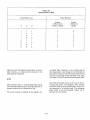
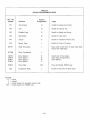
TABLE 3·3
OPTION PROGRAMMING GUIDE
WI-W3
Jumper
Function
Factory
Programmed
Usage
WI
Track Fault
0
Install for excess track fault.
W2
Test
0
Install for factory test.
W3
Disable Limit
0
Install to disable soft limits.
W4
Spin Select
0
Install for spin select.
W5
Tracks
S
Install for standard version only.
W6
Motor Type
-
Install for Type 1. gO motor.
RTW7
Read Terminator
I
WTWg
Write Terminator
I
S4W9
S3WlO
S2Wll
S1W12
Drive
Drive
Drive
Drive
0
3PW13
Three Disk
U22
Select 4
Select 3
Select' 2
Select 1
Close only at end drive of daisy chain data.
Closed for radial data.
Install one of four plugs
only. Plug corresponds to
drive address.
0
0
I
503
Terminator Pack
Install in end drive of daisy chain.
I
NOTES:
o
=
I
S
503
=
=
=
Close for Model TM503 only.
Omit
Install
Close jumper for standard version only.
Close jumper for TM503 only.
3-15
STEP A.
ENCLOSE UN IT IN POLY BAG
TO AVOID SURFACE
SCRATCHES AND
OTHER DAMAGE
STEP 8.
MOLD POLYURETHANE
"CLAMSHELL" TO ·CUBE" UNIT
FIGURE 3·11
RECOMMENDED SHIPPING PACK DESIGN,
CONFIGURATION 1
3-16
I NNER CARDBOARD
CONTA INER
CLAMSHEL L
STEP C.
FOAM COVER
STEP
0.1
AFTER CLOSI NG,
TAPE BOX ON ALL
R
SEAMS WITH 2 OR ' 3
WIDE FIBERGLASS
RE INFORCED
SHIPPING TAPE
I
I
INNER CONTAINER
,
OUTER CARDBOARD
CONTAINER
FIGURE 3·11 (CONTINUED)
RECOMMENDED SHIPPiNG PACK DESIGN,
CONFIGURATION 1
3-17
f1
STEP A.
ENCLOSE UNIT IN POLY BAG
TO AVOID SURFACE
SCRATCHES AND
OTHER DAMAGE
FOAM COVER
STEP B.
FOAM
AFTER CLOSI NG/
TAPE BOX ON ALL
SEAMS WITH 2" OR 3"
WIDE FIBERGLASS
REINFORCED
SHIPPING TAPE
OUTER CARDBOARD
CONTAINER
FIGURE 3·12
RECOMMENDED SHIPPING PACK DESIGN,
CONFIGURATION 2
3-18
STEP A.
ENCLOSE UNIT IN POLY BAG
TO AVOID SURFACE
SCRATCHES AND
OTHER DAMAGE
STEP B.
MOLDED POLYURETHANE
"CLAMSHELL# TO \'CUBEN UNIT
FIGURE 3·13
RECOMMENDED SHIPPING PACK DESIGN,
CONFIGURATION 3
3-19
CLAMSHELL /INNER CARDBOARD
CONTAINER
STEP C.
FOAM COVER
FOAM
STEP
AFTER CLOSI NG,
TAPE BOX ON ALL
SI DES WITH 2'.1 OR 3"
WIDE FIBERGLASS
REI NFORCED
SH I PPI NG TAPE
INNER CONTAINER
~-
OUTER CARDBOARD
CONTAINER
FIGURE 3·13 (CONTINUED)
RECOMMENDED SHIPPING PACK DESIGN
CONFIGURATION 3
3-20
P
0
L
Y
E
T
H
E
/
P
0
L
Y
E
S
T
E
R
14
FOAM DENSITY
1-1/4 LBS.
12
10
FOAM DENSITY
2-1;2 LBS.
8
6
4
2
F
0
A
M
*
.10
.20
.30
LOAD
FACTOR
**
.40
.50
NOTE
THE GRAPH GIVES FOAM THICKNESSES TO
SATISFY 10 G MINIMUM SHOCK LOADS ON
STANDARD 30 INCH DROP TEST
HENCE,ALL PACKAGE DESIGNS
SHOULD BE TESTED TO VERI FY · THEI R
ULTI MATE PERFORMANCE .
.*
THICKNESS IS IN INCHES.
**THE LOAD FACTOR IS IN LBS. PER SQ. INCH.
THE FORMULA IS : LOAD FACTOR = UNIT'S WEIGHT (LBS)
SMALLEST SIDE OF
UNIT (SO. INCHES)
FIGURE 3·14
LOAD GRAPH
3-21
,I
lani:liiii
CORPORATE OFFICES
20320 PRAIRIE STREET
CHATSWORTH, CA 91311
TEL. NO.: (213) 993-6644
TELEX NO.: 194794
TWX NO.: 910-494-1721
PIN 179043-00IA (T5002 A 1-83)
PRINTED IN U.S.A.