1
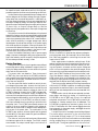
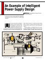
An Example of Intelligent Power-Supply Design B y KKeith eith CCuu rrtis tis tis,, Principal Applications Engineer, Microchip Technology, Chandler, Ariz. A low pin-count microcontroller enhances the features and functionality of a switching regulator. dard features common to a switching power-supply design. However, this design exploits the power of the microcontroller to add a number of novel programmable features. One such feature is an adaptive current limit control that lets the designer specify separate current limit values for different phases of the power supply’s operation. It’s possible to program an elevated current limit at startup 1 uF C3 R16 1 0.1 uF R20 3 In Vcc Out 10R 4 U74 IRF7493 TPS2818 2 CT1 U4 BAT54S CT321-100 U8 2 1 BZX84C20 3 A K D9 R22 1k C15 R23 100 pF 10 R 10 k R14 1k J3 6.8 k Cal R10 C2 R11 33 k 1 uF 10 k PICkit 1 Flash programming connector P5 1 2 3 4 5 6 7 8 9 10 11 12 13 14 HDR1314 P4 1 2 3 Vpp 4 5 6 7 ICSPDAT 8 ICSPCLK 9 10 11 12 13 14 HDR1314 P3 1 2 3 4 5 6 7 8 9 10 11 12 13 14 RA5 RA4 RA3 RC5 RC4 RC3 RA0 RA1 RA2 RC0 RC1 RC2 D5 D6 5 80SQ040 U3 IRF7493 4 10R 5, 6, 7, 8 1, 2, 3 68 k C11 C4 1.5 nF R15 R17 3.3 k 0.1 nF C10 2.2 nF C9 5 C8 C12 1 0.1 uF 3 In Vcc Out U74 R21 TPS2818 2 C5 0.47 uF C7 0.01 uF 3 D7 L1 80SQ040 T1 1 6 270 uH 2 5 PCV-2-274-10 3 4 D8 80SQ040 R9 47 k D4 Vdd C20 C21 C22 C23 1 nF 1 nF 0.1 uF 0.1 uF J1 C16 C18 C17 C19 100 uF 100 uF 100 uF 100 uF T4953107M016AS +5 V out J2 R7 5.1 k J6 +5 V LL4148 C1 0.1 uF U1 1 PIC16F684 2 Vdd 8 3 RA5 RC2 9 4 RA4 RC1 10 5 RA3 RC0 11 6 RC5 RA2 12 7 RC4 RA1 13 RC3 RA0 Vss 14 R5 R4 2 9 8 5 6 7 R19 U5 UC3847 Vin Sync 10 Vref Vc 13 Rt Aout 11 4 Ct +C/S +E/A B out 14 3 -E/A -C/S Comp CS SS 1 Sh-dh GND 16 12 15 10 k +5 V 2.2 k R12 0.47 uF C14 2200 uF 25 V GND Vdd 5A +24 V supply C13 2200 uF 25 V J5 80SQ040 F1 GND Vdd J4 +5 V C6 0.1 uF 1 U2 TC1047 Vdd R8 Out 2 5.1 k Gnd P8 22 k Trigger supply P9 R6 U 10 k sing a microcontroller to manage the operation of a switching power supply allows designers to implement new programmable features previously unavailable from stand-alone controller chips. Many of these features can be demonstrated with the design of a 24-V to 5-V dc-dc buck regulator. This design may seem generic because it has many of the stan- 3.3 k R2 Power good Temperature Overcurrent GND D1 Power good D1 Temperature 3.3 k R1 D1 Overcurrent R3 3.3 k Vdd HDR1314 Fig. 1. Hardware schematic of the power supply. Power Electronics Technology September 2004 28 www.powerelectronics.com POWER-SUPPLY DESIGN for capacitive loads, a reduced current limit for high-temperature operation and the normal operating current limit. Another feature is programmable output voltage, which lets the designer set the output voltage through programming rather than a manual adjustment. A calibration option also allows the designer to do an automated setting of the output voltage by simply connecting a reference voltage to the output and powering up the supply with a jumper in place. Also, an output voltage ramp-up lets the designer specify the speed at which the output voltage rises on power up. Using the microcontroller allows designers to implement supervisory features, such as a programmable undervoltage lockout, that makes the minimum supply-voltage requirements a programmed value rather than a manual adjustment. Another possibility is a trigger voltage input, which lets designers coordinate the startup of the power supply with other supplies in the system. Other options are an output overcurrent detect that doesn’t use a high-side current sense, an automatic power-up restart in the event of a serious fault and a retry counter to limit restarts. Most of the features listed aren’t new to power-supply design. However, the designer’s ability to program and configure the features, as well as specify complex sequences for the startup and fault recovery, is new. Fig. 2. Power-supply test hardware. 10 bits of resolution to generate the reference voltage input to the power chain, and a second 6-bit to 8-bit resolution PWM was needed for controlling the current limit input to the UC3847. Other requirements included a multiple-input 10-bit analog-to-digital converter for monitoring the various levels in the power chain, and an EEPROM memory for storing configuration constants and the output-voltage set point. Low-current operation also would be sought, so the microcontroller could be powered from the reference voltage in the UC3847. Because of the microcontroller’s scaling of the reference voltage, it would be necessary for the PWM output driver to be powered by the reference. Also, the ability to reprogram and configure the microcontroller required that the device have Flash program memory. The microcontroller selected to fit the requirements was a Microchip PIC16F684. In addition to meeting the design requirements, its small size (14 pins), low cost and the availability of low-cost development tools recommended it for the design. Once the main control devices were selected, the hardware design was simply a matter of interfacing the PIC16F684 to the UC3847 and filling in the required peripheral components. The UC3847 and its power chain are based on a design example from its datasheet. The PIC16F684’s programming interface is taken from the PICkit 1 Flash Starter Kit user’s manual. Fig. 1 shows the final schematic for the power supply, and Fig. 2 shows the final development board. A couple of points in the design should be highlighted. The power-supply connection to the microcontroller is connected through jumper J6. This is done because the power supply for the microcontroller must be isolated during programming so the programmer can properly reset the part. The bypass capacitance on the microcon- Design Overview Once specifications for the buck regulator were defined, the next step was to design hardware to support them. For clarity, the design was broken into two sections: the power chain and the microcontroller. The power chain was based on Texas Instruments’ UC3847 chip. Not a new device, the UC3847 provided access to several internal signals required for the features described above. Specifically, it allowed access to the Vref input of the error amplifier. The microcontroller had to be able to control the output voltage of the power chain. Access to the Vref input of the error amplifier was needed so the microcontroller could inject its own variable reference voltage in place of the UC3847’s reference. Access to the UC3847’s voltage reference also provided a convenient supply voltage for the microcontroller and gave the microcontroller’s variable reference voltage the same stability as the original reference. Another feature of the UC3847, an external currentlimit input, allowed the microcontroller to set the limit for the power chain. The UC3847 also offered access to the output of the error amplifier. Measuring this voltage allowed the microcontroller to determine the average output current of the power chain. The combination of the UC3847’s easy access to internal signals and the general controllability of the device made it a good candidate for the power-chain controller. The choice of a microcontroller also was influenced by the features required for the design. Two PWM outputs were needed. One output would require a minimum of www.powerelectronics.com 29 Power Electronics Technology September 2004 POWER-SUPPLY DESIGN prudent for any design that uses a Crnt_lmt_sm0 Current microcontroller limit Vsupply with in-circuit Vtrigger Control_sm0 Temperature Monitor_sm0 programming. Verror amp Many features Vout Out_volts_sm0 Output associated with the voltage power supply are implemented in Fig. 3. Software control and dataflow diagram. software. This is advantageous in that changes and uptroller supply must also be below 0.5 grades are just a matter of reprogramµF for proper programming. ming. The disadvantage is that the Also noteworthy is the combinasoftware design becomes more comtion of an isolation diode and a pullplex, requiring the ability to handle up resistor on pin RA3 of the multiple simultaneous operations. microcontroller. These components Handling simultaneous operation prevent the leakage of the 12-V proor multitasking is accomplished by gramming voltage into the 5-V supbuilding the software using state maply during programming. Furtherchine constructs. Much like hardware more, all control pins on the UC3847 state machines, software state mathat are driven by the microcontroller chines use a counter to sequence their are biased to their inactive states with operation. Based on the value, or state, a large-value resistor to keep the deof the counter, the state machine exvice inactive until the microcontroller ecutes different software functions. exits reset following power up. These The current state and external inputs design precautions are reasonable and Cal jumper Yokogawa's SignalExplorer and ScopeCorder families of digital oscilloscopes may be the best kept secret in test & measurement. However, it becomes less of a secret every year as more engineers discover the unique capabilities that Yokogawa's scopes offer. Request a two week, no-commitment evaluation of one of our scopes and discover for yourself the secret to making your most complicated measurements easier. K E Y F E A T U R E S of the SignalExplorer and ScopeCorder Families ■ Lots of Channels - Both Analog and Logic ■ Long Memory ■ I 2C, CAN and SPI - Triggering / Analysis ■ Power Analysis ■ Full-size and Portable Scopes ■ Easy PC Interface To discover more about Yokogawa’s scopes, contact your local Yokogawa representative or go to: promo.us.yokogawa.com and enter key code AD9409. are then combined to determine the next state to be executed. Multitasking is done by building separate state machines for the various functions that operate simultaneously, and calling them, one after the other, inside an infinite loop. This system allows each state machine to execute one state each time through the loop. The overall effect is that all state machines appear to be operating simultaneously, although slower than if executed individually. For this power-supply controller design, four state machines were written: Monitor_sm(), Control_sm(), Crnt_lmt_sm() and Out_volt_sm(). Control_sm() coordinates the activity of the other state machines and sets the overall operational “mood” of the system. Monitor_sm() performs all of the analog-to-digital conversion for the system, monitoring the supply, output, error amplifier and trigger voltages, as well as the temperature of the power MOSFET. Crnt_lmt_sm() controls the loop timing for the system and generates the current limit control voltage. Finally, Out_volt_sm() controls the output voltage of the power supply and generates the ramp-up function on power up. Fig. 3 shows how the control and data flows through the state machines. Monitor_sm() is a simple state machine that continuously cycles through the various analog signals, converting each into a 10-bit number for storage in the measured[] array. The sequence is supply voltage, trigger voltage, transistor temperature, error amplifier, and output voltage, before looping back to the supply voltage. The exception to the sequence is for the calibration mode. When calibrating, Monitor_sm() repeatedly converts only the output voltage signal, as the power chain is inactive. Control_sm() directs the activity of all the other state machines through its state-variable mood. The state machine’s states correspond to the six moods of the system. Based on the value of the mood state variable, the system’s other state machines alter their states accordingly to coordinate CIRCLE 225 on Reader Service Card or freeproductinfo.net/pet Power Electronics Technology September 2004 30 www.powerelectronics.com No one makes better tantalum capacitors and inductors. NEC TOKIN Tantalum Capacitors NEC TOKIN SMD Chip Inductors Innovation, performance, product quality and reliability. NEC TOKIN is the first and the best. We introduced the world’s first tantalum capacitors in 1955. We led the way in innovation and development. Now we offer you some of the smallest lead-free, largecapacitance capacitors for your high density, high frequency applications. Our power inductors feature some of the lowest profiles and best performance characteristics of the industry in a large selection of inductance values. You can rely on us, because we make your components from our own raw materials. Contact us now to receive the latest NEC TOKIN catalog. www .nec-tokinamerica.com Devices thru Material Innovation NEC TOKIN America, Inc. UNION CITY, CA / SAN DIEGO, CA / CHICAGO, IL / TAMPA, FL 32950 Alvarado-Niles Rd., Suite 500 Union City, CA 94587 Tel: 510-324-4110 Fax: 510-324-1762 NEC TOKIN Corporation Global Sales Headquarters: Tokyo, Japan Tel: 81-3-3402-6179 or visit www.nec-tokin.com Offices in Germany, UK, Hong Kong, Shenzhen, Shanghai, Taipei, Singapore, Malaysia, Bangkok, and Seoul CIRCLE 227 on Reader Service Card PowerorElectronics Technology September 2004 freeproductinfo.net/pet POWER-SUPPLY DESIGN their activity with the Control_sm(). The states of Control_sm() are Shutdown, Start, Normal, Iomax, Error and Cal. Shutdown is active when the power supply is waiting for the supply and trigger voltages to climb into their nominal ranges. Start is active when the output voltage is ramping up to its preset output voltage. Normal is active during all normal operation. Either Iomax or error is active during fault conditions. Iomax is for output overcurrent and Error is for an overtemperature condition. Cal is active in response to a request for calibration. But note that Cal is a dead-end state, requiring a powerdown to exit. Fig. 4 shows the states of Control_sm() and the possible state transitions, with their causes. The circles denote the specific state, with the arrow denoting a transition. The tag on each arrow notes the specific condition causing the transition. Crnt_lmt_sm() performs three functions. It synchronizes the start of each pass through the loop by delaying until the hardware timer Timer0 rolls over from FF to 00. Then, Crnt_lmt_sm() generates the current limit PWM output pulse before moving on to execute the current state. The Crnt_lmt_sm() has four possible states: Shutdown, Boost, Normal and Reduce. The Shutdown state holds the current limit PWM output at a duty cycle of zero, forcing the UC3847 to shut down the output of the power supply. The Boost state increases the current-limit duty cycle during the ramp-up of the output voltage. The Normal state sets the current limit duty cycle to the steadystate current limit. Reduce reduces the current limit duty cycle in response to a high-temperature condition in the power chain transistors. The transitions from state to state in the Cnrt_lmt_sm() state machine occur in response to changes in the systems, as indicated by the mood state variable. Fig. 5 shows the transition diagrams for the Crnt_lmt_sm() state machine. Out_volt_sm() operates in much the same way as Crnt_lmt_sm(), with 32 Powerup Shutdown Vsupply good Vtrigger good Cal jumper present Cal Vsupply low Rampup complete Normal Over current Hot Current OK IOmax Start Cool Error Hi temperature Fig. 4. Control_sm() state transition diagram. Powerup Shutdown Error Shutdown start cal Reduce Shutdown cal Start Normal Boost Error Normal error Normal Fig. 5. Crnt_lmt_sm() state transition diagram. a few exceptions. It doesn’t contain the timer monitoring or pulse generation sections, and it uses three states, not four: Shutdown, Ramp and Normal. Shutdown and Normal behave like the Shutdown and Normal states in Crnt_lmt_sm(), driving the output voltage PWM to zero for Shutdown, and to the preprogrammed setpoint during Normal operation. The new state is Ramp, in which Out_volt_sm() ramps up the output voltage over time, using increment and delay values set by the designer. Once the ramp up of the output is complete, Control_sm() is notified and the mood of the system and its state machines change to Normal. Fig. 6 diagrams Out_volt_sm(). When combined, the four state machines create a single management system that monitors and controls the operation of the power supply, rewww.powerelectronics.com POWER-SUPPLY DESIGN Shutdown Shutdown cal Start Normal error Shutdown Ramp start cal Normal error Normal Fig. 6. Out_volt_sm() state transition diagram. sponding to both internal and external events based on configuration values stored in the microcontroller’s EEPROM memory. Another issue in power-supply design is reliability. With the inclusion of a managing microcontroller, additional mechanisms must exist within the hardware and software design of the microcontrollers for handling fault conditions. Hardware reliability involves two concerns—the behavior of the microcontroller at power-up/ power-down and its response to EMI/ RFI. Software concerns are limited to detecting and correcting fault conditions that arise from corrupted data and/or programming memory. To manage the behavior of the microcontroller during power-up and power-down conditions, two systems are built into the microcontroller hardware: the power on reset (POR) circuit and the brownout reset (BOR) circuit. The POR circuit holds the microcontroller in reset during power-up until the supply voltage for the microcontroller reaches the minimum safe operating voltage and the main oscillator has stabilized. The BOR operates during powerdown, generating and holding a reset when the microcontroller power-supply voltage drops below the user-defined minimum supply voltage. Together, these two systems combine to hold the microcontroller in reset, whenever the power supply for the microcontroller is insufficient for stable operation of the device. Managing the microcontroller’s www.powerelectronics.com Intelligent MotionControl Enlarged View: 4x Size: 6mm2 the MC73110 Brushless MotorControllerIC • Ultra high-performance • Low cost • Sinusoidal or 6-step commutation • Internal profile generation • High-speed index capture • 6 signal PWM with shoot through protection • Digital current loop • Velocity loop The Best Engineered Products in Motion PERFORMANCEMOTIONDEVICES www.pmdcorp.com CIRCLE 228 on Reader Service Card or freeproductinfo.net/pet Author’s Note Thank you to Datatronics and Wirebenders for supplying the magnetic components in the design. For more information on this article, CIRCLE 334 on Reader Service Card 33 MOTORDRIVES AMPLIFIERS CONTROLLERS Power Electronics Technology © 2004 Performance Motion Devices, Inc. Powerup response to EMI and RFI is a matter of combining proper static protection for the device, proper selection of bypass capacitors and good layout. Good software design is important because EMI and RFI events can corrupt data and program memory. Although safeguards are implemented in software, they shouldn’t be taken as a license to neglect proper hardware protection. Two important software safeguards have been incorporated into this design to prevent unpredictable behavior by the software. The watchdog timer (WDT) is enabled and set for a time-out that is slightly longer than the worst-case timing for the main loop in the program. In addition, a clear WDT instruction exists in only one place, and that is in the main software loop. This protects the system from lockup conditions in the software by creating a means for the software to recover from a fault serious enough to have corrupted the program counter in the microcontroller. Another safeguard is the inclusion of a default state in all of the state decoding in the state machines. The default state is to be called whenever the state variable doesn’t decode to a valid state. Within the default state is a routine to reset all of the critical state machine data variables, including the state counter variable. Together, the hardware and software systems help the microcontroller recover from unpredictable behavior. Careful consideration of their use should be part of any design incorporating microcontroller management of a power-supply system. Those interested in building the power-supply design presented within the text of this article may visit http:// techtrain.microchip.com/downloads/ pet_0904.zip for a zipped file with source listings, a hex file, gerber files PETech and a bill of materials. September 2004