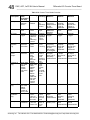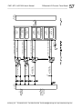
1
Series PMC424, APC424, AcPC424
24 Differential I/O and
16 TTL I/O with
4 Counter Timers
USER’S MANUAL
ACROMAG INCORPORATED
30765 South Wixom Road
P.O. BOX 437
Wixom, MI 48393-7037 U.S.A.
Copyright 2003, Acromag, Inc., Printed in the USA.
Data and specifications are subject to change without notice.
Tel: (248) 624-1541
Fax: (248) 624-9234
8500-709-D10B008
2
PMC, APC, AcPC424 User’s Manual
Differential I/O Counter Timer Board
__________________________________________________________________
TABLE OF
CONTENTS
IMPORTANT SAFETY CONSIDERATIONS
You must consider the possible negative effects of power, wiring,
component, sensor, or software failure in the design of any type of
control or monitoring system. This is very important where property
loss or human life is involved. It is important that you perform
satisfactory overall system design and it is agreed between you and
Acromag, that this is your responsibility.
1.0 General Information
The information of this manual
may change without notice.
Acromag makes no warranty
of any kind with regard to this
material, including, but not
limited to, the implied
warranties of merchantability
and fitness for a particular
purpose. Further, Acromag
assumes no responsibility for
any errors that may appear in
this manual and makes no
commitment to update, or
keep current, the information
contained in this manual. No
part of this manual may be
copied or reproduced in any
form without the prior written
consent of Acromag, Inc.
KEY 424 FEATURES……………………………………
PCI INTERFACE FEATURES……...…… ……… … ..
SIGNAL INTERFACE PRODUCTS..…… ……… … ..
Board DLL Control Software...……………….........
Board VxWORKS Software….………....…...………
Board QNX Software…......………….………...........
4
6
6
7
7
7
2.0 PREPARATION FOR USE
UNPACKING AND INSPECTION...…………………...
CARD CAGE CONSIDERATIONS.........……………..
BOARD CONFIGURATION..........................………...
Default Hardware Jumper Configuration.……
Front Panel I/O...…………………………………..
Rear J4 Field I/O Connector (PMC Only)……..
Non-Isolation Considerations...........................
8
8
8
8
9
10
10
3.0 PROGRAMMING INFORMATION
PCI CONFIGURATION ADDRESS SPACE.....……...
Configuration registers....…………………..…..
MEMORY MAP..............................................………...
Interrupt Register...............................................
Interrupt Status/Clear Counter/Timer…………
Interrupt Status/Clear Differential I/O…………
Interrupt Status/Clear Digital I/O…….…………
Differential Input/Output Registers..………….
Digital Input/Output Registers………………….
Direction Control Register………………...........
Interrupt Enable Registers..…………………….
Interrupt Type Configuration Registers..........
Interrupt Polarity Registers..……..…………….
Debounce Duration Select & Enable……...….
Counter Trigger Register....…………………….
Counter Stop Register.……………………….....
Counter Readback Registers....………………..
Counter Constant A Registers.………………...
Counter Constant B Registers..........................
Counter Control Registers..........……...............
Pulse Width Modulation......……...……...……...
Watchdog Timer Operation.……………...……..
Event Counting Operation..........................…...
11
11
12
14
15
15
16
16
17
17
18
18
19
20
21
21
22
22
22
23
24
26
28
_______________________________________________________________________________________
Acromag, Inc. Tel:248-624-1541 Fax:248-624-9234 Email:[email protected] http://www.acromag.com
PMC, APC, AcPC424 User’s Manual
Differential I/O Counter Timer Board
___________________________________________________________________
Frequency Measurement Operation.................
Input Pulse Width Measurement……………….
Input Period Measurement.……………………..
One-Shot Pulse Mode.........……………………..
PROGRAMMING EXAMPLES
Pulse Width Modulation Example....…...……...
Watchdog Timer Operation Example...............
Event Counting Operation Example.................
Frequency Measurement Operation Example.
Input Pulse Width Measurement Example.......
Input Period Measurement Example................
One-Shot Pulse Mode Example........................
30
32
34
36
38
38
39
40
42
43
45
46
3
TABLE OF
CONTENTS
4.0 THEORY OF OPERATION
LOGIC/POWER INTERFACE...…......………………...
PCI INTERFACE LOGIC...……………………………..
DIGITAL INPUT/OUTPUT LOGIC………………..……
COUNTER TIMER CONTROL LOGIC..........………...
49
49
49
49
5.0 SERVICE AND REPAIR
SERVICE AND REPAIR ASSITANCE...……………...
PRELIMINARY SERVICE PROCEDURE...…………..
WHERE TO GET HELP…………………………………
50
50
50
6.0 SPECIFICATIONS
PHYSICAL..................................................................
ENVIRONMENTAL....…….……………………………..
RELIABILITY PREDICTION……………………………
DIFFERENTIAL INPUT/OUTPUT.....................……...
DIGITAL INPUT/OUTPUT.................................……...
COUNTER CLOCK FREQUENCIES………………….
BOARD CRYSTAL OSCILLATOR.............................
PCI LOCAL BUS INTERFACE………………………
51
51
53
53
54
55
55
55
APPENDIX
CABLE: MODEL 5028-432.........................................
TERMINATION PANEL: MODEL 5025-288..………..
56
56
DRAWINGS
4501-959 424 BLOCK DIAGRAM.......………………..
4501-960 424 RESISTOR LOCATION……………….
4501-919 CABLE 5028-432 (SHIELDED)..................
4501-920 TERMINATION PANEL 5025-288.......……
57
58
59
60
Trademarks are the property of their respective owners.
_______________________________________________________________________________________
Acromag, Inc. Tel:248-624-1541 Fax:248-624-9234 Email:[email protected] http://www.acromag.com
4
PMC, APC, AcPC424 User’s Manual
Differential I/O Counter Timer Board
__________________________________________________________________
1.0 GENERAL
INFORMATION
The 424 board has 24 differential input/output and 16 digital input/output
channels. In addition, four 16-bit multifunction counter/timers are provided.
The 16 digital input/output channels can be programmed for input or
output on a channel basis and are used for counter timer control. The 24
differential input/output channels are programmed for input or output on a 4channel port basis. All input channels can be enabled for change of state,
low, or high level transition interrupts.
Four 16-bit multifunction counters/timers can be configured for pulse
width modulated output, watchdog timer, event counter, frequency
measurement, pulse width measurement, period measurement, or one shot
pulse output. The four 16-bit counters can also be configured into two 32-bit
counter/timers.
Signal input noise spikes can be filtered with use of the debounce logic
provided on each of the input channels.
Table 1.1: The 424 boards are
available in standard and
extended temperature ranges
MODEL
PCI Mezzanine
Card
PCI Mezzanine
Card (Rear I/O)
16-bit
Counter
I/O Type
OPERATING
TEMPERATURE
RANGE
24 Differ. 0°C to +70°C
16 TTL
24 Differ. 0°C to +70°C
PMC424R
Four
15 TTL
24
Differ. 0°C to +70°C
APC424
Short PCI
Four
16 TTL
24 Differ. 0°C to +70°C
AcPC424
3U CompactPCI
Four
16 TTL
PCI
Mezzanine
24 Differ. -40°C to +85°C
PMC424E
Four
Card
16 TTL
PCI
Mezzanine
24 Differ. -40°C to +85°C
PMC424CC
Four
Card (Rear I/O)
15 TTL
Conduction Cooled
24
Differ.
APC424E
Short PCI
Four
-40°C to +85°C
16 TTL
24 Differ. -40°C to +85°C
AcPC424E 3U CompactPCI
Four
16 TTL
Note: PMC424R and PMC424CC are rear field I/O models, only. All other
models have front I/O. The PMC424RE model is replaced by the
PMC424CC model.
PMC424
KEY 424 FEATURES
Board Form
Factor
Four
•
16 Digital Input/Output Channels – Interface with up to 16 input/output
channels (15 Rear I/O channels for PMCxxxR models) which can be
configured for input or output on an individual channel basis. Four of
these signals are used for each enabled counter/timer.
•
24 Differential Input/Output Channels – 24 channels of differential
RS422 can be configured for input or output in groups of 4-channels.
•
Programmable Change of State/Level Interrupts – Interrupts are
software programmable for any bit Change-Of-State or level on all input
channels.
•
Input Signal Filtering Debounce Logic – Input signals can be filtered
from noise spikes. Four programmable debounce filter durations from
1.6μs to 3.2ms can be selected.
_______________________________________________________________________________________
Acromag, Inc. Tel:248-624-1541 Fax:248-624-9234 Email:[email protected] http://www.acromag.com
PMC, APC, AcPC424 User’s Manual
Differential I/O Counter Timer Board
___________________________________________________________________
•
Pulse Width Modulation – Each counter can be programmed for pulse
width modulation. The duration of the logic high and low levels of the
output signal can be independently controlled. An external gate signal
can also be used to start/stop generation of the output signal.
•
Watchdog Timer – Each counter can be configured as a countdown
timer for implementation as a watchdog timer. A gate-off signal is
available for use to stop the count down operation. Interrupt generation
upon a countdown to zero condition is available.
•
Event Counter – Each counter can be configured to count input pulses
or events. A gate-off signal is provided to control count-up or count
down with each event. Interrupt generation upon programmed count
condition is available.
•
Frequency Measurement – Each counter can be configured to count
how many active edges are received during a period defined by an
external count enable signal. An interrupt can be generated upon
measurement complete.
•
Pulse-Width or Period Measurement – Each counter can be
configured to measure pulse-width or waveform period. In addition, an
interrupt can be generated upon measurement complete.
•
One-Shot and Repetitive One-Shot – A one-shot pulse waveform may
also be generated by each counter. The duration of the pulse and the
delay until the pulse goes active is user programmable. A repetitive
one-shot can be initiated with repetitive trigger pulses.
•
Power Up and System Reset is Failsafe – For safety, the digital
channels are configured for input upon power-up.
5
KEY 424
FEATURES
_______________________________________________________________________________________
Acromag, Inc. Tel:248-624-1541 Fax:248-624-9234 Email:[email protected] http://www.acromag.com
6
PMC, APC, AcPC424 User’s Manual
Differential I/O Counter Timer Board
__________________________________________________________________
PCI INTERFACE FEATURES
SIGNAL INTERFACE
PRODUCTS
•
High density - Target board.
•
Field Connections – All counter/timer, digital I/O, and power
connections are made through a single 68-pin SCSI front panel I/O
connector. Models PMC424R and PMC424CC, only use a 64 pin rear
I/O connector.
•
32, 16, 8-bit I/O - Register Read/Write is performed through data
transfer cycles in the PCI memory space. All registers can be accessed
via 32, 16, or 8-bit data transfers.
•
Compatibility – Complies to PCI Local Bus Specification Revision 2.2.
Provides one multifunction interrupt. Board is 5V signaling compliant
and 3.3V signaling tolerant.
The following signal interface products are for front I/O models which are
accessed via a 68 pin SCSI-3 front panel connector.
Cables and a termination panel are also available to interface with this
board.
See the Appendix for
further information on
these products.
Cable:
Model 5028-432: A 2-meter, round 68 conductor shielded cable with a
male SCSI-3 connector at both ends and 34 twisted pairs. The cable is
used for connecting the board to Model 5025-288 termination panels.
For optimum performance, use the shortest possible length of shielded
input cable.
Termination Panel:
Model 5025-288: DIN-rail mountable panel provides 68 screw terminals
for universal field I/O termination. Connects to Acromag board, via
SCSI-3 to twisted pair cable described above.
_______________________________________________________________________________________
Acromag, Inc. Tel:248-624-1541 Fax:248-624-9234 Email:[email protected] http://www.acromag.com
PMC, APC, AcPC424 User’s Manual
Differential I/O Counter Timer Board
___________________________________________________________________
7
Acromag provides a software product (sold separately) to facilitate the
development of Windows (98/Me/NT4/2000/XP®) applications accessing
Acromag PMC I/O board products, PCI I/O Cards, and CompactPCI I/O
Cards. This software (Model PCISW-API-WIN) consists of low-level drivers
and Windows 32 Dynamic Link Libraries (DLLs) that are compatible with a
number of programming environments including Visual C++™, Visual
Basic®, Borland C++ Builder® and others. The DLL functions provide a
high-level interface to boards eliminating the need to perform low-level
reads/writes of registers, and the writing of interrupt handlers.
BOARD DLL CONTROL
SOFTWARE
Acromag provides a software product (sold separately) consisting of
board VxWorks® software. This software (Model PMCSW-API-VXW) is
composed of VxWorks® (real time operating system) libraries for all
Acromag PMC I/O board products, PCI I/O Cards, and CompactPCI I/O
Cards. The software is implemented as a library of “C” functions which link
with existing user code to make possible simple control of all Acromag PMC
boards.
BOARD VxWORKS
SOFTWARE
Acromag provides a software product (sold separately) consisting of
board QNX® software. This software (Model PCISW-API-QNX) is
composed of QNX® (real time operating system) libraries for all Acromag
PMC I/O board products, PCI I/O Cards, and CompactPCI I/O Cards. The
software is implemented as a library of “C” functions which link with existing
user code to make possible simple control of all Acromag PMC boards.
BOARD QNX
SOFTWARE
_______________________________________________________________________________________
Acromag, Inc. Tel:248-624-1541 Fax:248-624-9234 Email:[email protected] http://www.acromag.com
8
PMC, APC, AcPC424 User’s Manual
Differential I/O Counter Timer Board
__________________________________________________________________
2.0 PREPARATION
FOR USE
UNPACKING AND
INSPECTION
Upon receipt of this product, inspect the shipping carton for evidence of
mishandling during transit. If the shipping carton is badly damaged or water
stained, request that the carrier's agent be present when the carton is
opened. If the carrier's agent is absent when the carton is opened and the
contents of the carton are damaged, keep the carton and packing material
for the agent's inspection.
For repairs to a product damaged in shipment, refer to the Acromag
Service Policy to obtain return instructions. It is suggested that salvageable
shipping cartons and packing material be saved for future use in the event
the product must be shipped.
WARNING: This board
utilizes static sensitive
components and should
only be handled at a staticsafe workstation.
CARD CAGE
CONSIDERATIONS
IMPORTANT: Adequate air
circulation or conduction
cooling must be provided to
prevent a temperature rise
above the maximum
operating temperature.
This board is physically protected with packing material and electrically
protected with an anti-static bag during shipment. However, it is
recommended that the board be visually inspected for evidence of
mishandling prior to applying power.
Refer to the specifications for loading and power requirements. Be sure
that the system power supplies are able to accommodate the power
requirements of the carrier/CPU board, plus the installed boards, within the
voltage tolerances specified.
Adequate air circulation must be provided to prevent a temperature rise
above the maximum operating temperature and to prolong the life of the
electronics. If the installation is in an industrial environment and the board is
exposed to environmental air, careful consideration should be given to airfiltering.
In a conduction cooled assembly, adequate thermal conduction must be
provided to prevent a temperature rise above the maximum operating
temperature.
BOARD
CONFIGURATION
Default Hardware Jumper
Configuration
Remove power from the system before installing board, cables,
termination panels, and field wiring.
The board may be configured differently, depending on the application.
When the board is shipped from the factory, it is configured as follows:
• J3 is open. Plus 3.3 volts is provided from an on board regulator.
• The default configuration of the programmable software control
register bits at power-up are described in section 3.
• The control registers must be programmed to the desired
configuration before starting data input or output operation.
_______________________________________________________________________________________
Acromag, Inc. Tel:248-624-1541 Fax:248-624-9234 Email:[email protected] http://www.acromag.com
PMC, APC, AcPC424 User’s Manual
Differential I/O Counter Timer Board
___________________________________________________________________
The front panel connector provides the field I/O interface connections. It
is a SCSI-3 68-pin female connector (AMP 787082-7 or equivalent)
employing latch blocks and 30 micron gold in the mating area (per MIL-G45204, Type II, Grade C). Connects to Acromag termination panel 5025288 from the front panel via round shielded cable (Model 5028-432).
9
Front Panel Field I/O
Connector
Differential channels 0 to 23 are controlled on an 4-bit port basis. Digital
channels 24 to 39 are controlled on an individual bit basis. The
counter/timer input and output control signals share Digital I/O channels 24
to 39. Each counter uses three input signals and one output signal. An
enabled counter/timer has its required input and output signals automatically
dedicated via the field connector. If the counter is not used then the ports
are available for independent channel digital I/O.
Pin Description
CH0+
CH0−
CH1+
CH1−
CH2+
CH2−
CH3+
CH3−
CH4+
CH4−
CH5+
CH5−
CH6+
CH6−
CH7+
CH7−
COMMON
COMMON
CH8+
CH8−
CH9+
CH9−
CH10+
CH10−
CH11+
CH11−
Digital CH24/Counter 1A
Digital CH25/Counter 1B
Digital CH26/Counter 1C
Digital CH27/Counter 1OUT
Digital CH28/Counter 2A
Digital CH29/Counter 2B
Digital CH30/Counter 2C
Digital CH31/Counter 2 OUT
Pin
1
2
3
4
5
6
7
8
9
10
11
12
13
14
15
16
17
18
19
20
21
22
23
24
25
26
27
28
29
30
31
32
33
34
Pin Description
COMMON
COMMON
CH12+
CH12−
CH13+
CH13−
CH14+
CH14−
CH15+
CH15−
CH16+
CH16−
CH17+
CH17−
CH18+
CH18−
CH19+
CH19−
CH20+
CH20−
CH21+
CH21−
CH22+
CH22−
CH23+
CH23−
Digital CH32/Counter 3A
Digital CH33/Counter 3B
Digital CH34/Counter 3C
Digital CH35/Counter 3 OUT
Digital CH36/Counter 4A
Digital CH37/Counter 4B
Digital CH38/Counter 4C
Digital CH39/Counter 4 OUT
Pin
35
36
37
38
39
40
41
42
43
44
45
46
47
48
49
50
51
52
53
54
55
56
57
58
59
60
61
62
63
64
65
66
67
68
Table 2.1: Board Field I/O Pin
Connections
The board has 4 TTL 16-bit
counters available. Two 16-bit
counters can be configured as
one 32-bit counter. If counters
1 and 2 were configured as a
32-bit counter, then the input
and output corresponding to
Counter 1 are used. Similarly,
counters 3 and 4 can also be
configured as 32-bit counters.
The signals corresponding to
the first counter in the pair will
be used.
_______________________________________________________________________________________
Acromag, Inc. Tel:248-624-1541 Fax:248-624-9234 Email:[email protected] http://www.acromag.com
10
PMC, APC, AcPC424 User’s Manual
Differential I/O Counter Timer Board
__________________________________________________________________
Rear J4 Field I/O Connector
On models with rear I/O, the J4 PMC connector provides the field I/O
interface connections. This connector is a 64-pin female receptacle header
(AMP 120527-1 or equivalent) which mates to the male connector on the
carrier/CPU board (AMP 120521-1 or equivalent).
Table 2.2: Board Rear Field
I/O Pin Connections
The board has 4 TTL 16-bit
counters available. Two 16-bit
counters can be configured as
one 32-bit counter. If counters
1 and 2 were configured as a
32-bit counter, then the input
and output corresponding to
Counter 1 are used. Similarly,
counters 3 and 4 can also be
configured as 32-bit counters.
The signals corresponding to
the first counter in the pair will
be used.
Non-Isolation
Considerations
Pin Description
Pin
Pin Description
CH0+
1
CH12+
CH0−
2
CH12−
CH1+
3
CH14+
CH1−
4
CH14−
CH2+
5
CH14+
CH2−
6
CH14−
CH3+
7
CH15+
CH3−
8
CH15−
CH4+
9
CH16+
CH4−
10
CH16−
CH5+
11
CH17+
CH5−
12
CH17−
CH6+
13
CH18+
CH6−
14
CH18−
CH7+
15
CH19+
CH7−
16
CH19−
CH8+
17
CH20+
CH8−
18
CH20−
CH9+
19
CH21+
CH9−
20
CH21−
CH10+
21
CH22+
CH10−
22
CH22−
CH11+
23
CH23+
CH11−
24
CH23−
Digital CH24/Counter 1A
25
Digital CH32/Counter 3A
Digital CH25/Counter 1B
26
Digital CH33/Counter 3B
Digital CH26/Counter 1C
27
Digital CH34/Counter 3C
Digital CH27/Counter 1OUT
28
Digital CH35/Counter 3 OUT
Digital CH28/Counter 2A
29
Digital CH36/Counter 4A
Digital CH29/Counter 2B
30
Digital CH37/Counter 4B
Digital CH30/Counter 2C
31
Digital CH38/Counter 4C
Digital CH31/Counter 2 OUT
32
COMMON
Note: On rear I/O models, Counter 4 Output is not connected to J4.
Pin
33
34
35
36
37
38
39
40
41
42
43
44
45
46
47
48
49
50
51
52
53
54
55
56
57
58
59
60
61
62
63
64
The board is non-isolated, since there is electrical continuity between the
logic and field I/O grounds. As such, the field I/O connections are not
isolated from the system. Care should be taken in designing installations
without isolation to avoid noise pickup and ground loops caused by multiple
ground connections. This is particularly important for analog inputs and
outputs when a high level of accuracy/resolution is needed.
_______________________________________________________________________________________
Acromag, Inc. Tel:248-624-1541 Fax:248-624-9234 Email:[email protected] http://www.acromag.com
PMC, APC, AcPC424 User’s Manual
Differential I/O Counter Timer Board
___________________________________________________________________
This Section provides the specific information necessary to program and
operate the board.
11
3.0 PROGRAMMING
INFORMATION
This board is a PCI Specification version 2.2 compliant PCI bus target
only board.
The PCI bus is defined to address three distinct address spaces: I/O,
memory, and configuration space. This board can be accessed via the PCI
bus memory space and configuration spaces, only.
The card’s configuration registers are initialized by system software at
power-up to configure the card. The board is a Plug-and-Play PCI card. As
a Plug-and-Play card the board’s base address and system interrupt request
line are not selected via jumpers but are assigned by system software upon
power-up via the configuration registers. A PCI bus configuration access is
used to read/write the PCI card’s configuration registers.
When the computer is first powered-up, the computer’s system
configuration software scans the PCI bus to determine what PCI devices are
present. The software also determines the configuration requirements of
the PCI card.
PCI Configuration
Address Space
The system software accesses the configuration registers to determine
how many blocks of memory space the carrier requires. It then programs
the board’s configuration registers with the unique memory base address.
The configuration registers are also used to indicate that the board
requires an interrupt request line. The system software then programs the
configuration registers with the interrupt request line assigned to the board.
Since this board is relocatable and not fixed in address space, its device
driver must use the mapping information stored in the board’s Configuration
Space registers to determine where the board is mapped in memory space
and which interrupt line will be used.
The PCI specification requires software driven initialization and
configuration via the Configuration Address space. This board provides 256
bytes of configuration registers for this purpose. It contains the
configuration registers, shown in Table 3.1, to facilitate Plug-and-Play
compatibility.
CONFIGURATION
REGISTERS
The Configuration Registers are accessed via the Configuration Address
and Data Ports. The most important Configuration Registers are the Base
Address Registers and the Interrupt Line Register which must be read to
determine the base address assigned to the board and the interrupt request
line that goes active on a board interrupt request.
_______________________________________________________________________________________
Acromag, Inc. Tel:248-624-1541 Fax:248-624-9234 Email:[email protected] http://www.acromag.com
12
PMC, APC, AcPC424 User’s Manual
Differential I/O Counter Timer Board
__________________________________________________________________
Table 3.1 Configuration
Registers
MEMORY MAP
Reg.
Num.
0
1
2
3
4
5 : 10
11
12
13,14
15
D31
D24
D23
D16
D15
D8
D7
D0
Device ID=4243
Vendor ID= 16D5
Status
Command
Class Code=118000
Rev ID=00
BIST
Header
Latency
Cache
32-bit Memory Base Address for 4K-Byte Block
Not Used
Subsystem ID=0000
Subsystem Vendor ID=0000
Not Used
Reserved
Max_Lat
Min_Gnt
Inter. Pin
Inter. Line
This board is allocated a 4K byte block of memory that is addressable in
the PCI bus memory space to control the boards multiple functions. Three
types of information are stored in the memory space: control, status, and
data.
The memory space address map for the board is shown in Table 3.2.
Note that the base address for the board in memory space must be added
to the addresses shown to properly access the board registers. Register
accesses as 32, 16, and 8-bit in memory space are permitted.
Table 3.2: Memory Map
1. The board will return 0 for
all addresses that are "Not
Used".
2. The board has 4 TTL 16-bit
counters available. Via
counter 1 control register, 16bit counters 1 and 2 can be
configured as one 32-bit
counter. This is also an option
for counter pairs 3 and 4.
3. The numbers in the left
most column represent the
User Manual page containing
a description of the
corresponding register
Base
Addr+
03
143
07
15
0B
15
0F
16
13
16
17
16
1B
17
1F
18
23
18
27
18
2B
18
2F
19
33
19
D31
D16
Interrupt Register
Not Used1
Counters 1 to 4 Interrupt
Status/Clear Reg.
Interrupt Status/Clear
15-0 Differential I/O
Interrupt Status/Clear
39-24 Digital TTL I/O
15-0 Differential I/O
Register
39-24 Digital TTL I/O
Register
Direction Register
Differential Channels 23-0
Interrupt Enable
Differential Channels 15-0
Interrupt Enable
Digital Channels 39-24
Interrupt Type
Differential Channels 15-0
Interrupt Type
Digital Channels 39-24
Interrupt Polarity
Differential Channels 15-0
Interrupt Polarity
Digital Channels 39-24
Not Used1
23-16 Differential
I/O Register
Not Used1
Direction Register
Dig. TTL Channels 39-24
Not
Interrupt Enable
Used1
Differential 23-16
Not Used1
Not
Used1
Interrupt Type
Differential 23-16
Not Used1
Not
Used1
D00
Not Used1
Interrupt Status/Clear
23-16 Differential I/O
Not
Used1
D15
Interrupt Polarity
Differential 23-16
Not Used1
Base
Addr+
00
04
08
0C
10
14
18
1C
20
24
28
2C
30
_______________________________________________________________________________________
Acromag, Inc. Tel:248-624-1541 Fax:248-624-9234 Email:[email protected] http://www.acromag.com
PMC, APC, AcPC424 User’s Manual
Differential I/O Counter Timer Board
___________________________________________________________________
37
21
23
23
23
23
22
223
22
22
22
20
20
20
20
20
Counter Trigger Register
34
3B
Counter 1 Control Register
(32-bit Counter Control Register)2
38
3F
Counter 2 Control Register
3C
43
Counter 3 Control Register
(32-bit Counter Control Register)2
40
47
Counter 4 Control Register
44
4B
Counter 2 Read Back
Counter 1 Read Back
Register
Register
Counter 4 Read Back
Counter 3 Read Back
Register
Register
Counter 2
Counter 1
Constant A Register
Constant A Register
Counter 4
Counter 3
Constant A Register
Constant A Register
Counter 2
Counter 1
Constant B Register
Constant B Register
Counter 4
Counter 3
Constant B Register
Constant B Register
Debounce Duration Select and Enable
Channels 0 to 7
Debounce Duration Select and Enable
Channels 8 to 15
Debounce Duration Select and Enable
Channels 16 to 23
Debounce Duration Select and Enable
Channels 24 to 31
Debounce Duration Select and Enable
Channels 32 to 39
4F
22
Counter Stop Register
53
57
5B
5F
63
67
6B
6F
73
77
Not Used1
48
4C
13
MEMORY MAP
When a 32-bit counter is
enabled, the readback and
constant registers of the two
16-bit counters that make the
32-bit counter become 32-bit
register values.
50
54
58
3. The numbers in the left
most column represent the
User Manual page containing
a description of the
corresponding register.
5C
60
64
68
6C
70
74
↓
FFF
Not Used1
FFC
This memory map reflects byte accesses using the “Little Endian” byte
ordering format. Little Endian uses even-byte addresses to store the loworder byte. The Intel x86 family of microprocessors uses “Little Endian” byte
ordering. Big Endian is the convention used in the Motorola 68000
microprocessor family and is the VMEbus convention. In Big Endian, the
lower-order byte is stored at odd-byte addresses.
_______________________________________________________________________________________
Acromag, Inc. Tel:248-624-1541 Fax:248-624-9234 Email:[email protected] http://www.acromag.com
14
PMC, APC, AcPC424 User’s Manual
Differential I/O Counter Timer Board
__________________________________________________________________
INTERRUPT
REGISTERS
Interrupt Register (Read/Write) – (Base + 00H)
This read/write register is used to enable board interrupt operation,
determine the pending status of interrupts, and release pending interrupts.
The function of each of the interrupt register bits is described in Table
3.3. This register can be read or written with either 8-bit, 16-bit, or 32-bit
data transfers. A power-up or system reset sets all interrupt register bits
to 0.
Table 3.3: Interrupt Register
BIT
FUNCTION
0
1
1. All bits labeled “Not Used”
will return logic “0” when read.
2 to 13
14
15
Board Interrupt Enable Bit. (Read/Write Bit)
0 = Disable Interrupt
1 = Enable Interrupt
If enabled via this bit an interrupt request from the board will
be issued to the system upon any of its interrupt conditions.
The interrupt request will remain active until the interrupt
release bit is set, or by disabling interrupts via this bit.
Board Interrupt Pending Status Bit. (Read Only Bit)
0 = Interrupt Not Pending
1 = Interrupt Pending
This bit can be read to determine the interrupt pending status
of the board. When this bit is logic “1” an interrupt is pending
and will cause an interrupt request if bit-0 of the register is
set. When this bit is a logic “0” an interrupt is not being
requested. Once the bit is in the pending status it will remain
until the pending interrupt is removed via the source of the
interrupt. This bit will remain active even if interrupts are
disabled via bit-0.
When this bit is set the pending interrupt can originate from
any of the 4 counter timers, the 24 differential I/O, or 16
digital I/O channels. To identify the source of the pending
interrupt base address plus 04H is read to identify a
Counter/Timer Interrupt, while base address plus 08H is read
to identify a differential input interrupt, and 0CH is read to
identify a digital input Interrupt.
Not Used1
Software Reset: The board is reset.
Not Used1
_______________________________________________________________________________________
Acromag, Inc. Tel:248-624-1541 Fax:248-624-9234 Email:[email protected] http://www.acromag.com
PMC, APC, AcPC424 User’s Manual
Differential I/O Counter Timer Board
___________________________________________________________________
Interrupt Status/Clear Counter/Timer Register (Read/Write)
– (Base + 04H)
15
INTERRUPT
REGISTERS
This read/write register is used to determine the pending status of
Counter/Timer interrupts, and release pending Counter/Timer interrupts.
The Counter/Timer interrupt status/clear bits 0 to 3 reflect the status of
each of the Counter/Timers. Read of this bit reflects the interrupt pending
status. Read of a “1” indicates that an interrupt is pending for the
corresponding counter/timer. Write of a logic “1” to this bit to release a
counter timer pending interrupt. Writing “0” to a bit location has no effect, a
pending interrupt will remain pending. The Counter/Timer and its
corresponding interrupt Pending/Clear bits are as shown in Table 3.4.
BIT
0
1
2
3
4-31
FUNCTION
Counter/Timer 1 Interrupt Pending/Clear
Counter/Timer 2 Interrupt Pending/Clear
Counter/Timer 3 Interrupt Pending/Clear
Counter/Timer 4 Interrupt Pending/Clear
Not Used1
Table 3.4: Board
Counter/Timer Interrupt
Status/Clear
1. All bits labeled “Not Used”
will return logic “0” when
read.
The board has 4 TTL 16-bit counters available. Two 16-bit counters can
be configured as one 32-bit counter. For example, counter 1 and 2 can be
combined to form a 32-bit counter. A counter configured as a 32-bit counter
has its interrupt status/clear function controlled via the odd counter. For
example, counter 3 and 4 when combined have their interrupt status/clear
function controlled via bit-2.
Interrupt Status/Clear Differential I/O (Read/Write) –
(Base + 08H)
This read/write register is used to determine the pending status of
Differential input interrupts, and release pending Differential input interrupts.
The Differential input interrupt status/clear registers reflect the status of
each of the Differential channels. Read of this bit reflects the interrupt
pending status. Read of a “1” indicates that an interrupt is pending for the
corresponding differential channel. Write of a logic “1” to this bit releases
the corresponding differential channel’s pending interrupt. Writing “0” to a
bit location has no effect, a pending interrupt will remain pending.
Differential input channel 0 interrupt status is identified via data bit-0
while Differential input channel 23 status is identified via data bit-23 at base
address plus 08H.
Reg.
Num.
08H
D31
D24
Not Used
D23
D16
D15
D8
D7
D0
23-0 Differential Input Interrupt Status/Clear Bits
_______________________________________________________________________________________
Acromag, Inc. Tel:248-624-1541 Fax:248-624-9234 Email:[email protected] http://www.acromag.com
16
PMC, APC, AcPC424 User’s Manual
Differential I/O Counter Timer Board
__________________________________________________________________
DIGITAL
INPUT/OUTPUT
REGISTERS
Interrupt Status/Clear Digital TTL (Read/Write) –
(Base + 0CH)
This read/write register is used to determine the pending status of Digital
TTL input interrupts, and release pending Digital TTL interrupts.
The Digital TTL interrupt status/clear registers reflect the status of each
of the Digital TTL channels. Read of this bit reflects the interrupt pending
status. Read of a “1” indicates that an interrupt is pending for the
corresponding Digital TTL channel. Write of a logic “1” to this bit releases
the corresponding Digital TTL channel’s pending interrupt. Writing “0” to a
bit location has no effect, a pending interrupt will remain pending.
Digital TTL input channel 24 interrupt status is identified via data bit-0
while Digital TTL input channel 39 status is identified via data bit-15 at base
address plus 0CH.
Reg.
Num.
0CH
D31
D24
D23
Not Used
D16
D15
D8
D7
D0
39-24 Digital TTL Interrupt
Status/Clear Bits
Differential Input/Output Register (Read/Write) –
(Base + 10H)
Twenty-four differential channels numbered 0 through 23 may be
individually accessed via this register. Channels 23 to 0 are accessed at the
carrier base address +10H via data bits 23 to 0. Channel input signal levels
are determined by reading this register. Likewise, channel output signal
levels are set by writing to this register. Note the data direction, input or
output, must first be set via the Direction register at base address plus 18H.
Channel read/write operations use 8-bit, 16-bit, or 32-bit data transfers
with the lower ordered bits corresponding to the lower-numbered channels
for the register of interest. All input/output channels are configured as inputs
on a power-on or software reset.
_______________________________________________________________________________________
Acromag, Inc. Tel:248-624-1541 Fax:248-624-9234 Email:[email protected] http://www.acromag.com
PMC, APC, AcPC424 User’s Manual
Differential I/O Counter Timer Board
___________________________________________________________________
Digital Input/Output Registers (Read/Write) –
(Base + 14H)
Sixteen possible input/output channels numbered 24 through 39 may be
individually accessed via these registers. Channels 39 to 24 are accessed
at the carrier base address +14H via data bits 15 to 0. Channel input signal
levels are determined by reading this register. Likewise, channel output
signal levels are set by writing to this register. Note the data direction, input
or output, must first be set via the Direction register at base address plus
1AH.
17
DIGITAL
INPUT/OUTPUT
REGISTERS
Channel read/write operations use 8-bit, 16-bit, or 32-bit data transfers
with the lower ordered bits corresponding to the lower-numbered channels
for the register of interest. All input/output channels are configured as inputs
on a power-on or software reset.
Ch 31
D7
Ch 39
D15
Digital I/O Channel and Corresponding Register Bits
Ch 30
Ch 29
Ch 28
Ch 27
Ch 26
Ch 25
D6
D5
D4
D3
D2
D1
Ch 38
D14
Ch 37
D13
Ch 36
D12
Ch 35
D11
Ch 34
D10
Ch 33
D9
Ch 24
D0
Ch 32
D8
Direction Control Register (Read/Write) - (Base + 18H)
The data direction (input or output) of the 24 differential channels and 16
digital channels is selected via this register. The data direction of channels
0 to 23 is controlled as groups of 4 bits. Channels 0 to 23 are set/controlled
via bits 0 to 5 as shown below. The data direction of digital channels 24 to
39 is controlled on an individual channel basis via bits 16 to 31 as shown
below. Setting a bit low configures the corresponding channel data direction
for input. Setting the control bit high configures the corresponding channel
data direction for output.
The counter/timer input and output control signals share Digital I/O
channels 24 to 39. Each counter uses three input signals and one output
signal. An enabled counter/timer has its required input and output signals
automatically set by hardware and control via this register is disabled. If the
counter is not used, then the ports are available for independent channel
digital I/O.
Ch23 - 20
D5
Channels and Corresponding Register Bits
Ch19 - 16 Ch15 - 12
Ch11 - 8
Ch7 - 4
D4
D3
D2
D1
Ch3 - 0
D0
Ch 31
D23
Ch 30
D22
Ch 29
D21
Ch 28
D20
Ch 27
D19
Ch 26
D18
Ch 25
D17
Ch 24
D16
Ch 39
D31
Ch 38
D30
Ch 37
D29
Ch 36
D28
Ch 35
D27
Ch 34
D26
Ch 33
D25
Ch 32
D24
_______________________________________________________________________________________
Acromag, Inc. Tel:248-624-1541 Fax:248-624-9234 Email:[email protected] http://www.acromag.com
18
PMC, APC, AcPC424 User’s Manual
Differential I/O Counter Timer Board
__________________________________________________________________
The default power-up state of these registers is logic low. Thus, all
channels are configured as inputs on system reset or power-up. Register
bits D6 to D15 of this register are “Not Used” and will always read low (0’s).
Reading or writing to this register is possible via 32-bit, 16-bit or 8-bit data
transfers.
DIGITAL INTERRUPT
REGISTERS
Interrupt Enable Registers (Read/Write) –
(Base + 1CH and 20H)
The Interrupt Enable Registers provide a mask bit for each of the 40
channels. A “0” bit will prevent the corresponding input channel from
generating an external interrupt. A “1” bit will allow the corresponding
channel to generate an interrupt.
The Interrupt Enable register at the base address + offset 1CH is used to
control differential channels 0 through 23 via data bits 0 to 23. Digital
channels 39 to 24 are accessed at the carrier base address +20H via data
bits 15 to 0.
All channel interrupts are disabled (set to “0”) following a power-on or
software reset. Reading or writing to this register is possible via 32-bit, 16bit or 8-bit data transfers.
Interrupt Type (COS or H/L) Configuration Registers
(Read/Write) - (Base + 24H and 28H)
The Interrupt Type Configuration Registers determine the type of input
channel transition that will generate an interrupt for each of the 40 possible
interrupting channels. A “0” bit selects interrupt on level. An interrupt will be
generated when the input channel level specified by the Interrupt Polarity
Register occurs (i.e. Low or High level transition interrupt). A “1” bit means
the interrupt will occur when a Change-Of-State (COS) occurs at the
corresponding input channel (i.e. any state transition, low to high or high to
low).
The Interrupt Type Configuration register at base address + offset 24H is
used to control differential channels 0 through 23. For example, channel 0
is controlled via data bit-0. Digital channels 39 to 24 are accessed at the
carrier base address +28H via data bits 15 to 0. For example, channel 24 is
controlled via data bit-0.
All bits are set to “0” following a reset which means that, if enabled, the
inputs will cause interrupts for the levels specified by the digital input
channel Interrupt Polarity Register.
Channel read or write operations use 8-bit, 16-bit, or 32-bit data
transfers. Note that no interrupts will occur unless they are enabled by the
Interrupt Enable Register.
_______________________________________________________________________________________
Acromag, Inc. Tel:248-624-1541 Fax:248-624-9234 Email:[email protected] http://www.acromag.com
PMC, APC, AcPC424 User’s Manual
Differential I/O Counter Timer Board
___________________________________________________________________
Interrupt Polarity Registers (Read/Write) –
(Base + 2CH and 30H)
19
DIGITAL INTERRUPT
REGISTERS
The Interrupt Polarity Register determines the level that will cause a
channel interrupt to occur for each of the channels enabled for level
interrupts. A “0” bit specifies that an interrupt will occur when the
corresponding input channel is low (i.e. a “0” in the digital input channel data
register). A “1” bit means that an interrupt will occur when the input channel
is high (i.e. a “1” in the digital input channel data register). Note that no
interrupts will occur unless they are enabled by the Interrupt Enable
Register. Further, the Interrupt Polarity Register will have no effect if the
Change-of-State (COS) interrupt type is configured by the Interrupt Type
Configuration Register.
The Interrupt Polarity register at the carrier’s base address + offset 2CH
is used to control differential channels 0 through 23. Digital channels 39 to
24 are accessed at the carrier base address +30H via data bits 15 to 0. For
example, digital channel 24 is controlled via data bit-0.
All bits are set to “0” following a reset which means that the inputs will
cause interrupts when they are logic low (provided they are enabled for
interrupt on level).
_______________________________________________________________________________________
Acromag, Inc. Tel:248-624-1541 Fax:248-624-9234 Email:[email protected] http://www.acromag.com
20
PMC, APC, AcPC424 User’s Manual
Differential I/O Counter Timer Board
__________________________________________________________________
DEBOUNCE DURATION
REGISTERS
Debounce Duration Select and Enable Registers
(Read/Write) – (Base + 60H to 70H)
This register controls debounce enable and duration selection for each of
the 40 digital channels. Debounce, when enabled, will filter noise present
on a channel’s input line. All noise spikes with a duration less than the
debounce time, selected via Table 3.5, are ignored when present on the
input signal/channel.
Table 3.5a: Debounce
Duration Select
Not Used Bits: 3, 7, 11, 15,
19, 23, 27, and 31 will return
logic “0” when read.
Reg.
Bits
2,1,0
6,5,4
10,9,8
14,13,12
18,17,16
22,21,20
26,25,24
30,29,28
Channels and Corresponding Register Bits
Offset Address
60H
64H
68H
6CH
Ch0
Ch8
Ch16
Ch24
Ch1
Ch9
Ch17
Ch25
Ch2
Ch10
Ch18
Ch26
Ch3
Ch11
Ch19
Ch27
Ch4
Ch12
Ch20
Ch28
Ch5
Ch13
Ch21
Ch29
Ch6
Ch14
Ch22
Ch30
Ch7
Ch15
Ch23
Ch31
70H
Ch32
Ch33
Ch34
Ch35
Ch36
Ch37
Ch38
Ch39
The bits listed in the Register Bits column above must be set as shown in
the Debounce Duration Select Table 3.5b.
Table 3.5b: Debounce
Duration Select
BIT
000
001
010
011
100
101 ,110, 111
FUNCTION
Debounce Disabled
1.6μs
10.4μs
408.8μs
3.276ms
Reserved
For example, to enable channel 33 and channel 37 for a debounce level
of 10.4μs, and 3.276ms respectively, the value 400020H must be written to
base address plus 70H. Notice bits 3, 7, 11, 15, 19, 23, 27, and 31 are don’t
care bits and are represented by an “X” in the following table. Note that
writing 400020 Hex, to base address plus 70H, also disables debounce for
channels 32, 34, 35, 36, 38, and 39.
Ch39
X000
0
Disable
Ch38
Ch37
Bits 31 down to 16
X000
X100
0
4
Disable
3.27ms
Ch36
Ch35
X000
0
X000
0
Disable
Disable
Ch34
Ch33
Bits 15 down to 0
X000
X010
0
2
Disable
10.4μs
Ch32
X000
0
Disable
The Debounce Duration Select and Enable register bits are set to “0”
following reset. Thus, on reset and power-up debounce will be disabled by
default. These registers are read/write registers that can be accessed with
8-bit, 16-bit, or 32-bit data transfers.
_______________________________________________________________________________________
Acromag, Inc. Tel:248-624-1541 Fax:248-624-9234 Email:[email protected] http://www.acromag.com
PMC, APC, AcPC424 User’s Manual
Differential I/O Counter Timer Board
___________________________________________________________________
Counter Trigger Register (Write) - (Base + 34H)
21
COUNTER REGISTERS
This register is used to implement software triggering for all counter
timers. Writing a 1 to the counter’s corresponding trigger bit of this register
will cause the counter function to be triggered. Table 3.6 identifies the
trigger bit location corresponding to each of the counters. The contents of
this register are not stored and merely act to trigger the corresponding
counters.
BIT
0
1
2
3
4-15
FUNCTION
Counter 1 Trigger
Counter 2 Trigger
Counter 3 Trigger
Counter 4 Trigger
Not Used1
(32-bit Counter Trigger)
(32-bit Counter Trigger)
Table 3.6: Board Counter
Trigger Register
1. All bits will return logic “0”
when read
Triggering may be used to initiate pulse width modulation, watchdog
timer (initiates countdown), event counting, frequency measurement, pulsewidth measurement, period measurement, or one-shot.
Writing to this register is possible via 32-bit, 16-bit or 8-bit data transfers.
Counter Stop Register (Read/Write) - (Base + 36H)
This register is used to stop one or a group of Counter/Timers. Writing a
“1” to the counter’s corresponding stop bit of this register will cause the
counter to be disabled. That is, bits 2,1, and 0 of the counter control register
are cleared to “000”, thus disabling and stopping the counter. Table 3.7
identifies the stop bit location corresponding to each of the counters. The
bits of this register are not stored and merely act to stop the corresponding
counter when set to logic high.
Writing to this register is possible via 32-bit, 16-bit or 8-bit data transfers.
BIT
16
17
18
19
20-31
FUNCTION
Counter 1 Stop (32-bit Counter Stop)
Counter 2 Stop
Counter 3 Stop (32-bit Counter Stop)
Counter 4 Stop
Not Used1
Table 3.7: Board Counter
Stop Register
1. All bits will return logic “0”
when read
_______________________________________________________________________________________
Acromag, Inc. Tel:248-624-1541 Fax:248-624-9234 Email:[email protected] http://www.acromag.com
22
PMC, APC, AcPC424 User’s Manual
Differential I/O Counter Timer Board
__________________________________________________________________
COUNTER REGISTERS
Counter Readback Registers (Read Only) –
(Base + 48H and 4CH)
The Counter Readback register is a dynamic function register that
returns the current value held in the counter. It is updated with the value
stored in the internal counter, each time it is read.
The internal counter is generally initialized with the value in the Counter
Constant Register, and its value is incremented or decremented according
to the application.
The Counter Readback register at base address + offset 48H
corresponds to counters 1 and 2. Counters’ 3 and 4 Readback registers are
accessed at the carrier base address +4CH.
This register must be read using 32-bit long-word accesses for 32-bit
enabled counters, but it may be read using 16-bit accesses for 16-bit
enabled counters.
Note that the Counter
Constant Registers are
cleared (set to 0) following
a system or software reset.
Counter Constant A Registers (Write Only) –
(Base + 50H and 54H)
This write-only register is used to store the counter/timer constant A
value (initial value) for the various counting modes. Accesses to this
register are allowed on a 16-bit or 32-bit long-word basis, only. It is
necessary to load the constant value into the counter in one clock cycle.
Thus, for a 16-bit counter a 16-bit or 32-bit write access is required, while a
32-bit write access is required for a 32-bit counter.
Base address + offset 50H corresponds to the Counter Constant A
register for counters 1 and 2. Base address + offset 54H corresponds to the
Counter Constant A register for counters 3 and 4.
Counter Constant B Registers (Read/Write) –
(Base + 58H and 5CH)
This read/write register is used to store the counter/timer constant B
value. It is necessary to load the constant value into the counter in one
clock cycle. Thus, for a 16-bit counter a 16-bit or 32-bit write access is
required, while a 32-bit write access is required for a 32-bit counter.
Base address + offset 58H corresponds to the Counter Constant B
register for counters 1 and 2. Base address + offset 5CH corresponds to
the Counter Constant B register for counters 3 and 4.
_______________________________________________________________________________________
Acromag, Inc. Tel:248-624-1541 Fax:248-624-9234 Email:[email protected] http://www.acromag.com
PMC, APC, AcPC424 User’s Manual
Differential I/O Counter Timer Board
___________________________________________________________________
Counter Control Registers (Read/Write) –
(Base + 38H, 3CH, 40H, 44H)
23
COUNTER CONTROL
REGISTERS
This register is used to configure counter/timer functionality. It defines
the counter mode, output polarity, input polarity, clock source, counter size,
and interrupt enable.
The memory map addresses corresponding to the control registers are
given in Table 3.2. The Counter Control Register is cleared (set to 0)
following a reset, thus disabling the counter/timer. Reading or writing to this
register is possible via 32-bit, 16-bit, or 8-bit data transfers.
The board has four 16-bit Counter/Timers. A pair of counters can be
grouped to form a 32-bit counter. Control register bit-14 when set high
enables 32-bit counter mode. When a 32-bit counter is enabled it must be
selected via control register 1 for counters 1 and 2. Likewise, control
register 3 is used when counters 3 and 4 are enabled as a 32-bit counter.
The counter timer functions of the board provide seven modes of
operation: pulse width modulation, watchdog timer, event counting,
frequency measurement, pulse width measurement, period measurement,
and one-shot pulse mode. The following sections describe the features of
each method of operation and how to best use them.
_______________________________________________________________________________________
Acromag, Inc. Tel:248-624-1541 Fax:248-624-9234 Email:[email protected] http://www.acromag.com
24
PMC, APC, AcPC424 User’s Manual
Differential I/O Counter Timer Board
__________________________________________________________________
COUNTER CONTROL
REGISTERS
Pulse Width Modulation
Pulse width modulated waveforms may be generated at the counter
timer output. The pulse width modulated waveform is generated
continuously. Pulse Width Modulation generation is selected by setting
Counter Control Register bits 2 to 0 to logic “010”.
Counter Constant A value controls the time until the pulse goes active.
The duration of the pulse is set via the Counter Constant B register. Note
that a high pulse will be generated if active high output is selected while a
low pulse will be generated if active low output is selected.
The counter goes through a countdown sequence for each Counter
Constant value. When the 0 count is detected, the output toggles to the
opposite state. Then the second Counter Constant value is loaded into the
counter, and countdown resumes, decrementing by one for each rising edge
of the clock selected via Control Register bits 12, 11, and 10. For example,
a counter constant value of 3 will provide a pulse duration of 3 clock cycles
of the selected clock. Note, when the internal 20MHz clock is selected, a
delay of one extra clock cycle will be added to the counter constant value.
InA can be used as a Gate-Off signal to stop and start the counter and
thus the pulse-width modulated output. When InA is enabled via bits 5 and
4 of the control register for active low Gate-Off input, a logic low input will
enable pulse-width modulation counting while a logic high will stop PWM
counting. When InA is enabled for active high Gate-Off operation, a logic
high will enable PWM counting while a logic low will stop PWM counting.
InB can be used to input an external clock for use in PWM. Bits 7 and 6
must be set to either logic “01” or “10”. Additionally, the clock source bits
12, 11, and 10 must be set to logic “101” to enable external clock input.
PWM can alternatively be clocked via an internal 1.25MHz, 2.5MHz, 5MHz,
10MHz, or 20MHz clock as selected via control register bits 12, 11, and 10.
InC can be used to externally trigger Pulse Width Modulation generation.
Additionally PWM can be triggered internally via the Counter Trigger
Register at the base address + offset 34H. An initial trigger, software or
external, causes the pulse width modulated signal to be generated. After an
initial trigger, do not issue additional triggers. Triggers issued while running
will cause the Constant A and B values to load at the wrong time. In
addition, changing the Control register setting while running can also cause
the Constant A and B values to load at the wrong time.
If the Interrupt Enable bit of the Counter Control Register is set (bit 15)
and bit-0 of the Interrupt register is set, an interrupt is generated when the
output pulse transitions from low to high and also for transitions from high to
low. Thus, an interrupt is generated at each pulse transition.
_______________________________________________________________________________________
Acromag, Inc. Tel:248-624-1541 Fax:248-624-9234 Email:[email protected] http://www.acromag.com
PMC, APC, AcPC424 User’s Manual
Differential I/O Counter Timer Board
___________________________________________________________________
Bit(s)
2,1,0
3
5, 4
7, 6
9,8
12,11,10
13
14
15
FUNCTION
Specifies the Counter Mode:
010
Pulse Width Modulation
Output Polarity (Output Pin ACTIVE Level):
0
Active LOW (Default)
1
Active HIGH
InA Polarity / Gate-Off Polarity
00
Disabled (Default)
Active LOW
01
In A=0; Counter is Enabled
In A=1; Counter is Disabled
Active HIGH
10
In A=0 Counter is Disabled
In A=1 Counter is Enabled
11
Disabled
InB Polarity / External Clock Input
00
Disabled (Default)
01
External Clock Enabled
10
External Clock Enabled
11
Disabled
InC Polarity / External Trigger
00
Disabled (Default)
01
Active LOW External Trigger
10
Active HIGH External Trigger
11
Disabled
Clock Source
000
Internal @ 1.25MHz (Default)
001
Internal @ 2.5MHz
010
Internal @ 5MHz
011
Internal @ 10MHz
100
Internal @ 20MHz
101
External Clock (Up to 8MHz)
Not Used (bit is read as logic “0”)
Counter Size:
0
16-bit Counter (Default)1
1
32-bit Counter
Interrupt Enable
0
Disable Interrupt Service (Default)
1
Enable Interrupt Service
25
COUNTER CONTROL
REGISTERS
Pulse Width Modulation
Table 3.8: Counter Control
Register
(Pulse Width Modulation)
1. When two 16-bit counters
are selected to implement a
32-bit counter the control
register corresponding to the
first 16-bit counter is used for
control of the 32 bit counter.
_______________________________________________________________________________________
Acromag, Inc. Tel:248-624-1541 Fax:248-624-9234 Email:[email protected] http://www.acromag.com
26
PMC, APC, AcPC424 User’s Manual
Differential I/O Counter Timer Board
__________________________________________________________________
COUNTER CONTROL
REGISTERS
Watchdog Timer Operation
The watchdog operation counts down from a programmed (Counter
Constant A) value until it reaches 0. While counting, the counter output will
be in its active state (the output polarity is programmable). Upon time-out,
the counter output will return to its inactive state, and an optional interrupt
may be generated. Watchdog operation is selected by setting Counter
Control Register bits 2 to 0 to logic “011”.
A timed-out watchdog timer will not re-cycle until it is reloaded and then
followed with a new trigger. Failure to cause a reload would generate an
automatic time-out upon re-triggering, since the counter register will contain
the 0 it previously counted down to.
InA input can be used to reload the counter with the Constant A register
value. InA reload input is enabled via Control register bits 5 and 4. The
counter can also be reloaded via a software write to the Counter Constant A
register. Writing to the Counter Constant A register will load the value
directly into the counter even if watchdog counting is active.
InB can be used to input an external clock for watchdog timing. Bits 7
and 6 must be set to either logic “01” or “10”. Additionally, the clock source
bits 12, 11, and 10 must be set to logic “101” to enable external clock input.
The timer can alternatively be clocked via an internal 1.25MHz, 2.5MHz,
5MHz, 10MHz, or 20MHz clock as selected via control register bits 12, 11,
and 10.
InC can be used to either continue/stop watchdog counting or as an
external trigger input. When control register bits 9 and 8 are set to logic
“11”, InC functions as a Continue/Stop signal. When the Continue/Stop
signal is high the counter continues counting (when low the counter stops
counting). Alternately, when control register bits 9 and 8 are set to logic “01”
or “10”, the InC input functions as an external trigger input. The watchdog
timer may also be internally triggered (via the Trigger Control Register at the
base address + offset 34H).
When triggered, the counter/timer contents are decremented by one for
each clock cycle, until it reaches 0, upon which a watchdog timer time-out
occurs. For example, a counter constant value of 30 will provide a time-out
delay of 30 clock cycles of the selected clock. However, due to the
asynchronous relationship between the trigger and the selected clock, one
clock cycle of error can be expected. The counter can be read from the
Counter Readback register at any time during watchdog operation.
Upon time-out, the counter output pin returns to its inactive state. The
board will also issue an interrupt upon detection of a count value equal to 0,
if enabled via bit-15 of the Counter Control Register and bit-0 of the Interrupt
register. This could be useful for alerting the host that a watchdog timer
time-out has occurred and may need to be reinitialized. The interrupt will
remain pending until the watchdog timer is reinitialized and the interrupt is
released by setting the required bit of the Counter/Timer Interrupt
Status/Clear register.
_______________________________________________________________________________________
Acromag, Inc. Tel:248-624-1541 Fax:248-624-9234 Email:[email protected] http://www.acromag.com
PMC, APC, AcPC424 User’s Manual
Differential I/O Counter Timer Board
___________________________________________________________________
Bit(s)
2,1,0
3
5, 4
7, 6
9,8
12,11,10
13
14
15
FUNCTION
Specifies the Counter Mode:
011
Watchdog Function
Output Polarity (Output Pin ACTIVE Level):
0
Active LOW (Default)
1
Active HIGH
InA Polarity / Counter Reload
00
Disabled (Default)
Active LOW
01
In A=0 Counter Reinitialized
In A=1 Inactive State
Active HIGH
10
In A=0 Inactive State
In A=1 Counter Reinitialized
11
Disabled
InB Polarity / External Clock Input
00
Disabled (Default)
01
External Clock Enabled
10
External Clock Enabled
11
Disabled
InC Polarity / External Trigger
00
Disabled (Default)
01
Active LOW Trigger
10
Active HIGH Trigger
11
Gate-Off (Continue when high/Stop when low)
Clock Source
000
Internal @ 1.25MHz (Default)
001
Internal @ 2.5MHz
010
Internal @ 5MHz
011
Internal @ 10MHz
100
Internal @ 20MHz
101
External Clock (Up to 8MHz)
Not Used (bit is read as logic “0”)
Counter Size:
0
16-bit Counter (Default)1
1
32-bit Counter
Interrupt Enable
0
Disable Interrupt Service (Default)
1
Enable Interrupt Service
27
COUNTER CONTROL
REGISTERS
Watchdog Timer
Operation
Table 3.9: Counter Control
Register (Watchdog Timer)
1. When two 16-bit counters
are selected to implement a
32-bit counter the control
register corresponding to the
first 16-bit counter is used for
control of the 32 bit counter.
_______________________________________________________________________________________
Acromag, Inc. Tel:248-624-1541 Fax:248-624-9234 Email:[email protected] http://www.acromag.com
28
PMC, APC, AcPC424 User’s Manual
Differential I/O Counter Timer Board
__________________________________________________________________
COUNTER CONTROL
REGISTERS
Event Counting Operation
Positive or negative polarity events can be counted. Event Counting is
selected by setting Counter Control Register bits 2 to 0 to logic “100” and
setting bits 12 to 10 to logic “000”.
Input pulses or events occurring at the input InB of the counter will
increment the counter until it reaches the Counter Constant A value. Upon
reaching the count limit, an output pulse of 1.6μs will be generated at the
counter output pin, and an optional interrupt may be generated.
Additionally, the internal event counter is cleared. The counter will continue
counting, again from 0, until it reaches the Counter Constant A value. Once
triggered, event counting will continue until disabled via Control register bits
2 to 0.
InA can be used as a Gate-Off signal to stop and start event counting.
When InA is enabled via bits 5 and 4 of the control register for active low
Gate-Off input, a logic low input will enable event counting while a logic high
will stop event counting. When InA is enabled for active high Gate-Off
operation, a logic high will enable event counting while a logic low will stop
event counting.
InB is used as the event input signal. Active high or low input events can
be selected via Control register bits 7 and 6. A minimum event pulse width
(InB) of 100ns is required for correct pulse detection with input debounce
disabled. Programmable clock selection is not available in event counter
mode.
InC can be used to either control up/down counting or as an external
trigger input. When control register bits 9 and 8 are set to logic “11”, InC
functions as an Up/Down signal. When the Up/Down signal is high the
counter is in the count down mode (when low the counter counts up). The
counter will not count down below a count of zero. Alternately, when control
register bits 9 and 8 are set to logic “01” or “10”, the InC input functions as
an external trigger input. Event counting may also be internally triggered
(via the Trigger Control Register at the base address + offset 34H).
The Counter Constant A Register holds the count-to value (constant).
Reading the Counter Readback Register will return the current count
(variable). The Counter Constant A value must not be left as 0. The
counter upon trigger starts counting from 0 and since the counter would
match the count-to value the counter resets and starts counting from zero
again.
If the Interrupt Enable bit of the Counter Control Register is set (bit 15)
and bit-0 of the Interrupt register is set, an interrupt is generated when the
number of input pulse events is equal to the Counter Constant A register
value. The internal counter is then cleared and will continue counting
events until the counter constant A value is again reached and a new
interrupt generated. An interrupt will remain pending until released by
setting the required bit of the Counters Interrupt Status/Clear register at the
base address + offset 04H. A pending interrupt can also be cleared, by
setting Control register bit-15 to logic low.
_______________________________________________________________________________________
Acromag, Inc. Tel:248-624-1541 Fax:248-624-9234 Email:[email protected] http://www.acromag.com
PMC, APC, AcPC424 User’s Manual
Differential I/O Counter Timer Board
___________________________________________________________________
Bit(s)
2,1,0
3
5, 4
7, 6
9,8
12,11,10
13
14
15
FUNCTION
Specifies the Counter Mode:
100
Event Counting
Output Polarity (Output Pin ACTIVE Level):
0
Active LOW (Default)
1
Active HIGH
InA Polarity / Gate-Off
00
Disabled (Default)
Active LOW
01
In A=0: Continue Counting
In A=1: Stop Counting
Active HIGH
10
In A=0: Stop Counting
In A=1: Continue Counting
11
Disabled
InB Polarity / Event Input
00
Disabled (Default)
01
Active LOW Events
10
Active HIGH Events
11
Disabled
InC Polarity / External Trigger
00
Disabled (Default)
01
Active LOW Trigger
10
Active HIGH Trigger
11
Up when logic low /Down when logic high
Specifies the Counter Mode:
000
Event Counting
Not Used (bit is read as logic “0”)
Counter Size:
0
16-bit Counter (Default)1
1
32-bit Counter
Interrupt Enable
0
Disable Interrupt Service (Default)
1
Enable Interrupt Service
29
COUNTER CONTROL
REGISTERS
Event Counting
Operation
Table 3.10: Counter Control
Register
(Event Counting)
1. When two 16-bit counters
are selected to implement a
32-bit counter the control
register corresponding to the
first 16-bit counter is used for
control of the 32 bit counter.
_______________________________________________________________________________________
Acromag, Inc. Tel:248-624-1541 Fax:248-624-9234 Email:[email protected] http://www.acromag.com
30
PMC, APC, AcPC424 User’s Manual
Differential I/O Counter Timer Board
__________________________________________________________________
COUNTER CONTROL
REGISTERS
Frequency Measurement Operation
Frequency Measurement is selected by setting Counter Control Register
bits 2 to 0 to logic “100” and setting bits 12 to 10 to logic “111”. The counter
counts how many InB edges (low to high or high to low) are received during
the InA enable interval. The frequency is the number of counts divided by
the duration of the InA enable signal.
InA is used as an enable signal to start frequency measurement. The
InA signal must be a pulse of known width. When InA is configured (via bits
5 and 4 of the control register) as an active low enable input, a logic low
input will enable frequency measurement while a logic high will stop
frequency measurement. When InA is configured as an active high enable
signal, a logic high will enable frequency measurement while a logic low will
stop frequency measurement.
InB is used to input the signal whose frequency is to be measured. Input
pulses occurring at input InB of the counter are counted while the enable
signal present on InA is active. When the InA signal goes inactive, the
counter output will generate a 1.6μs output pulse and an optional interrupt.
InC can be used as an external trigger input. When control register bits
9 and 8 are set to logic “01” or “10”, the InC input functions as an external
trigger input. Frequency measurement may also be internally triggered (via
the Trigger Control Register at the base address + offset 34H). An initial
trigger, software or external, starts frequency measurement upon the active
edge of the InA enable signal. Retrigger is required for a new frequency
measurement.
The Counter Constant A Register is not used for frequency
measurement. Do not write to this register while the counter is actively
counting since this will cause the counter to be loaded with the Constant A
value.
Reading the Counter Readback Register will return the current count
(variable). A minimum event pulse width (InB) of 100ns is required for
correct pulse detection with input debounce disabled. Programmable clock
selection is not available for frequency measurement.
If the Interrupt Enable bit-15 of the Counter Control Register is set and
bit-0 of the Interrupt register is set, an interrupt is generated when the input
InA enable pulse goes inactive. An interrupt will remain pending until
released by setting the required bit of the Counters Interrupt Status/Clear
register at the base address + offset 04H. A pending interrupt can also be
cleared, by setting the Counter Control register bit-15 to logic low.
_______________________________________________________________________________________
Acromag, Inc. Tel:248-624-1541 Fax:248-624-9234 Email:[email protected] http://www.acromag.com
PMC, APC, AcPC424 User’s Manual
Differential I/O Counter Timer Board
___________________________________________________________________
Bit(s)
2,1,0
3
5, 4
7, 6
9,8
12,11,10
13
14
15
FUNCTION
Specifies the Counter Mode:
100
Frequency Measurement
Output Polarity (Output Pin ACTIVE Level):
0
Active LOW (Default)
1
Active HIGH
InA Polarity / Enable Pulse of Known Width
00
Disabled (Default)
01
Active LOW Pulse
10
Active HIGH Pulse
11
Disabled
InB Polarity / Signal Measured/Counted
00
Disabled (Default)
01
Active LOW Pulse Counted
10
Active HIGH Pulse Counted
11
Disabled
InC Polarity / External Trigger
00
Disabled (Default)
01
Active LOW Trigger
10
Active HIGH Trigger
11
Disabled (Default)
Specifies the Counter Mode:
111
Frequency Measurement
Not Used (bit is read as logic “0”)
Counter Size:
0
16-bit Counter (Default)1
1
32-bit Counter
Interrupt Enable
0
Disable Interrupt Service (Default)
1
Enable Interrupt Service
31
COUNTER CONTROL
REGISTERS
Frequency
Measurement
Operation
Table 3.11: Counter Control
Register
(Frequency Measurement)
1. When two 16-bit counters
are selected to implement a
32-bit counter the control
register corresponding to the
first 16-bit counter is used for
control of the 32 bit counter.
_______________________________________________________________________________________
Acromag, Inc. Tel:248-624-1541 Fax:248-624-9234 Email:[email protected] http://www.acromag.com
32
PMC, APC, AcPC424 User’s Manual
Differential I/O Counter Timer Board
__________________________________________________________________
COUNTER CONTROL
REGISTERS
Input Pulse Width Measurement
Setting bits 2 to 0 of the Counter Control Register to logic “101”
configures the counter for pulse-width measurement. After pulse-width
measurement is triggered, the first input pulse is measured.
InA is used to input the pulse to be measured. An active low or high
pulse can be measured.
InB can be used to input an external clock for Pulse-Width Measurement.
Bits 7 and 6 must be set to either logic “01” or “10”. Additionally, the clock
source bits 12, 11, and 10 must be set to logic “101” to enable external clock
input. Pulse Width Measurement can alternatively be clocked via an internal
1.25MHz, 2.5MHz, 5MHz, 10MHz, or 20MHz clock as selected via control
register bits 12, 11, and 10.
InC can be used to externally trigger Pulse Width Measurement.
Additionally, Pulse Width Measurement can be triggered internally via the
Counter Trigger Register at the base address + offset 34H. An initial trigger,
software or external, starts pulse width measurement at the beginning of the
next active pulse.
For pulse-width measurement, the pulse-width being measured serves
as an enable control for an up-counter whose value can be read from the
Counter Readback Register. When triggered, the counter is reset and then
increments by one for each clock pulse while the input signal level remains
in the active state (high or low according to the programmed polarity of input
InA). The resultant pulse-width is equivalent to the count value read from
the Counter Readback Register, multiplied by the clock period. An output
pulse will be generated at the counter output pin to signal the completion of
a given measurement. Note that the measured pulse may be in error by ± 1
clock cycle.
A counter value of 0xFFFF hex for a 16-bit counter or 0xFFFFFFFF for a
32-bit counter indicates that the pulse duration is longer than the current
counter size and clock frequency can measure. Upon read of this overflow
value you must select a slower clock frequency and re-measure.
An interrupt can be generated upon completion of a given pulse width
measurement (the pulse has returned to the opposite polarity), if enabled via
the interrupt enable bit of the Counter Control Register (bit 15) and bit-0 of
the Interrupt register. The interrupt will remain pending until released by
setting the required bit of the Counter’s Interrupt Status/Clear register at the
base address + offset 04H. A pending interrupt can also be cleared, by
setting the Counter Control register bit-15 to logic low.
_______________________________________________________________________________________
Acromag, Inc. Tel:248-624-1541 Fax:248-624-9234 Email:[email protected] http://www.acromag.com
PMC, APC, AcPC424 User’s Manual
Differential I/O Counter Timer Board
___________________________________________________________________
Bit(s)
2,1,0
3
5, 4
7, 6
9,8
12,11,10
13
14
15
FUNCTION
Specifies the Counter Mode:
101
Pulse-Width Measurement
Output Polarity (Output Pin ACTIVE Level):
0
Active LOW (Default)
1
Active HIGH
InA Polarity / Pulse Polarity to be Measured
00
Disabled (Default)
01
Active LOW Pulse is Measured
10
Active HIGH Pulse is Measured
11
Disabled
InB Polarity / External Clock Input
00
Disabled (Default)
01
External Clock Enabled
10
External Clock Enabled
11
Disabled
InC Polarity / External Trigger
00
Disabled (Default)
01
Active LOW Trigger
10
Active HIGH Trigger
11
Disabled
Clock Source
000
Internal @ 1.25MHz (Default)
001
Internal @ 2.5MHz
010
Internal @ 5MHz
011
Internal @ 10MHz
100
Internal @ 20MHz
101
External Clock (Up to 8MHz)
Not Used (bit is read as logic “0”)
Counter Size:
0
16-bit Counter (Default)1
1
32-bit Counter
Interrupt Enable
0
Disable Interrupt Service (Default)
1
Enable Interrupt Service
33
COUNTER CONTROL
REGISTERS
Input Pulse Width
Measurement
Table 3.12: Counter Control
Register
(Input Pulse Width
Measurement)
1. When two 16-bit counters
are selected to implement a
32-bit counter the control
register corresponding to the
first 16-bit counter is used for
control of the 32 bit counter.
_______________________________________________________________________________________
Acromag, Inc. Tel:248-624-1541 Fax:248-624-9234 Email:[email protected] http://www.acromag.com
34
PMC, APC, AcPC424 User’s Manual
Differential I/O Counter Timer Board
__________________________________________________________________
COUNTER CONTROL
REGISTERS
Input Period Measurement
The counter/timer may be used to measure the period of an input signal
at the counter input InA. Setting bits 2 to 0 of the Counter Control Register
to logic “110” configures the counter for period measurement. The first input
cycle after period measurement is triggered will be measured.
InA is used to input the signal to be measured. Period measurement can
be initiated on the active low or high portion of the waveform. The period of
signal is the time the signal is low added to the time the signal is high,
before it repeats.
InB can be used to input an external clock for period measurement. Bits
7 and 6 must be set to either logic “01” or “10”. Additionally, the clock
source bits 12, 11, and 10 must be set to logic “101” to enable external clock
input. Period measurement can alternatively be clocked via an internal
1.25MHz, 2.5MHz, 5MHz, 10MHz, or 20MHz clock as selected via control
register bits 12, 11, and 10.
InC can be used to externally trigger period measurement. Additionally,
Period Measurement can be triggered internally via the Counter Trigger
Register at the base address + offset 34H. An initial trigger, software or
external, starts period measurement at the beginning of the next active
period.
The period being measured serves as an enable control for an upcounter whose value can be read from the Counter Readback Register.
When triggered the counter is reset. Then, the active polarity of InA starts
period measurement. The counter increments by one for each clock pulse
during the input signal period (InA). The resultant period is equivalent to the
count value read from the Counter Readback Register, multiplied by the
clock period. A 1.6μs output pulse will be generated at the counter output
pin to signal the completion of a given measurement. Note that the
measured period may be in error by ± 1 clock cycle.
A counter value of 0xFFFF hex for a 16-bit counter or 0xFFFFFFFF for a
32-bit counter indicates that the period duration is longer than the current
counter size and clock frequency can measure. Upon read of this overflow
value you must select a slower clock frequency and re-measure.
An interrupt can be generated upon completion of a given period
measurement, if enabled via the interrupt enable bit of the Counter Control
Register (bit 15) and bit-0 of the Interrupt register. The interrupt will be
generated upon completion of the first complete waveform cycle after the
counter is triggered. The interrupt will occur even if an external clock is
selected but no clock signal is provided on InB. The count value will be zero
in this case. The interrupt, once driven active, will remain pending until
released by setting the required bit of the Interrupt Status/Clear register at
the base address + offset 04H. A pending interrupt can also be cleared, by
setting Counter Control register bit-15 to logic low.
_______________________________________________________________________________________
Acromag, Inc. Tel:248-624-1541 Fax:248-624-9234 Email:[email protected] http://www.acromag.com
PMC, APC, AcPC424 User’s Manual
Differential I/O Counter Timer Board
___________________________________________________________________
Bit(s)
2,1,0
3
5, 4
7, 6
9,8
12,11,10
13
14
15
FUNCTION
Specifies the Counter Mode:
110
Period Measurement
Output Polarity (Output Pin ACTIVE Level):
0
Active LOW (Default)
1
Active HIGH
InA Polarity / Signal Measured
00
Disabled (Default)
Active LOW portion of the signal starts period
01
measurement.
Active HIGH portion of the signal starts period
10
measurement.
11
Disabled
InB Polarity / External Clock Input
00
Disabled (Default)
01
External Clock Enabled
10
External Clock Enabled
11
Disabled
InC Polarity / External Trigger
00
Disabled (Default)
01
Active LOW Trigger
10
Active HIGH Trigger
11
Disabled
Clock Source
000
Internal @ 1.25MHz (Default)
001
Internal @ 2.5MHz
010
Internal @ 5MHz
011
Internal @ 10MHz
100
Internal @ 20MHz
101
External Clock (Up to 8MHz)
Not Used (bit is read as logic “0”)
Counter Size:
0
16-bit Counter (Default)1
1
32-bit Counter
Interrupt Enable
0
Disable Interrupt Service (Default)
1
Enable Interrupt Service
35
COUNTER CONTROL
REGISTERS
Input Period
Measurement
Table 3.13: Counter Control
Register
(Input Period Measurement)
1. When two 16-bit counters
are selected to implement a
32-bit counter the control
register corresponding to the
first 16-bit counter is used for
control of the 32 bit counter.
_______________________________________________________________________________________
Acromag, Inc. Tel:248-624-1541 Fax:248-624-9234 Email:[email protected] http://www.acromag.com
36
PMC, APC, AcPC424 User’s Manual
Differential I/O Counter Timer Board
__________________________________________________________________
COUNTER CONTROL
REGISTERS
One-Shot Pulse Mode
One-Shot pulse mode provides an output pulse that is asserted one time
or repeated each time it is re-triggered. One-Shot generation is selected by
setting Counter Control Register bits 2 to 0 to logic “111”.
The Counter Constant A value controls the time until the pulse goes
active. The duration of the pulse high or low is set via the Counter Constant
B value. Note that the Constant B value defines the logic high pulse width, if
active high output is selected, and a low pulse if active low output is
selected.
The counter goes through a full countdown sequence for each Counter
Constant value. When the 0 count is detected, on the next rising-edge of
the clock, the output toggles to the opposite state, and the Counter Constant
B value is loaded into the counter and countdown resumes, decrementing
by one each clock cycle. For example, a counter constant value of 7 will
provide a pulse duration of 7 clock cycles of the selected clock, then 50ns
will be added for the count detection of 0.
InA can be used as a Gate-Off signal to stop and start the counter and,
thus output. When InA is enabled via bits 5 and 4 of the control register for
active low Gate-Off input, a logic low input will enable the one-shot counter
while a logic high will stop the one-shot counter. When InA is enabled for
active high Gate-Off operation, a logic high will enable the one-shot counter
while a logic low will stop the one-shot counter.
InB can be used to input an external clock for use in one-shot. Bits 7
and 6 must be set to either logic “01” or “10”. Additionally, the clock source
bits 12, 11, and 10 must be set to logic “101” to enable external clock input.
InC can be used to externally trigger One-Shot pulse mode. Additionally,
a one-shot pulse can be triggered internally via the Counter Trigger Register
at the base address + offset 34H. An initial trigger, software or external,
causes the one-shot signal to be generated with no additional triggers
required. Additional triggers must not be input until the one shot pulse has
completed count down of the Constant B value.
If the Interrupt Enable bit-15 of the Counter Control Register is set, and
bit-0 of the Interrupt register is set, an interrupt is generated when the pulse
transitions from low to high and also when the pulse transitions from high to
low. The interrupt will remain pending until released by setting the required
bit of the Counters Interrupt Status/Clear register at the base address +
offset 04H. A pending interrupt can also be cleared, by setting the Counter
Control register bit-15 to logic low.
_______________________________________________________________________________________
Acromag, Inc. Tel:248-624-1541 Fax:248-624-9234 Email:[email protected] http://www.acromag.com
PMC, APC, AcPC424 User’s Manual
Differential I/O Counter Timer Board
___________________________________________________________________
Bit(s)
2,1,0
3
5, 4
7, 6
9,8
12,11,10
13
14
15
FUNCTION
Specifies the Counter Mode:
111
One-Shot Generation
Output Polarity (Output Pin ACTIVE Level):
0
Active LOW (Default)
1
Active HIGH
InA Polarity / Gate-Off Polarity
00
Disabled (Default)
Active LOW
01
In A=0 Output Enabled
In A=1 Output Disabled
Active HIGH
10
In A=0 Output Disabled
In A=1 Output Enabled
11
Disabled
InB Polarity / External Clock Input
00
Disabled (Default)
01
External Clock Enabled
10
External Clock Enabled
11
Disabled
InC Polarity / External Trigger
00
Disabled (Default)
01
Active LOW Trigger
10
Active HIGH Trigger
11
Disabled
Clock Source
000
Internal @ 1.25MHz (Default)
001
Internal @ 2.5MHz
010
Internal @ 5MHz
011
Internal @ 10MHz
100
Internal @ 20MHz
101
External Clock (Up to 8MHz)
Not Used (bit is read as logic “0”)
Counter Size:
0
16-bit Counter (Default)1
1
32-bit Counter
Interrupt Enable
0
Disable Interrupt Service (Default)
1
Enable Interrupt Service
37
COUNTER CONTROL
REGISTERS
One-Shot Pulse Mode
Table 3.14: Counter Control
Register
(One-Shot Pulse)
1. When two 16-bit counters
are selected to implement a
32-bit counter the control
register corresponding to the
first 16-bit counter is used for
control of the 32 bit counter.
_______________________________________________________________________________________
Acromag, Inc. Tel:248-624-1541 Fax:248-624-9234 Email:[email protected] http://www.acromag.com
38
PMC, APC, AcPC424 User’s Manual
Differential I/O Counter Timer Board
__________________________________________________________________
PROGRAMMING
EXAMPLES
The following section provides sample applications for each of the
counter modes of operation. This includes I/O pin assignments, register
settings, required calculations, and waveform diagrams.
Pulse Width Modulation Example
Since Counter 3 is a 32-bit
counter, Counter 4 cannot
be used.
The objective for this example is to create a pulse width modulated with
an active high pulse of 2μs and a low pulse of 6μs using 16-bit Counter 3.
The counter has an external active high gate-off, trigger, and clock signals.
The output is active high. Assume the external clock has a frequency of
500KHz. The Gate-Off signal will become active after 2 PWM cycles.
Additionally, interrupts are enabled.
1. Connect the inputs/output to the following pins (unpowered):
Table 3.17: PWM Pin
Assignments for Counter 3
Note: Make sure all inputs
and outputs are properly
grounded.
Pin #
61
62
63
64
Connection
In3_A(+)
In3_B(+)
In3_C(+)
Out3(+)
Description
Gate-Off
Ext. Clock
Ext. Trigger
Output
2. Write the following information, 966AH, to Counter 3 Control Register
located at base address plus an offset of 40H.
Table 3.18: PWM Counter
Control Register 3 Settings
1. Make sure that bit 0 at
base address plus an offset
0H is set to enable interrupts.
Bits
2,1,0
3
5,4
7,6
9,8
12,11,10
13
14
15
Logic
010
1
10
01
10
101
0
0
1
Operation
Sets the counter to Pulse Width Modulation mode.
Sets the output to active high.
Enable the Gate-Off input (InA) to active high.
Enables the external clock input (InB).
Enables the external Trigger Input (InC) to active high.
Sets the clock to an external source.
Not Used
Select a 16-bit counter size for use.
Enables interrupts.1
3. Write the 16-bit value 3H to Counter 3 Constant A Register located at
base address plus an offset 54H for the non-active portion of the pulse, and
1H to Counter 3 Constant B Register located at base address plus an offset
5CH for the active portion of the pulse.
In order to determine the necessary Counter Constant values first
calculate the period of the selected clock (internal or external). The period
is calculated by taking the inverse of the clock frequency. In this case,
1/500KHz is equal to 2μs. Then take the total time for the low portion of the
pulse and divide it by the clock period. For this example, 6μs/2μs is equal to
3. Convert this value to Hex and the result is the total count that is placed in
the appropriate Counter Constant Register. Since it has been stipulated
that the pulse is active high, 3H is written to Counter 3 Constant A Register,
which contains the value for the non-active (low) portion of the pulse. The
same procedure is used to calculate the Constant B value. Take the total
period of the high portion of the pulse and divide it by the period of the clock.
_______________________________________________________________________________________
Acromag, Inc. Tel:248-624-1541 Fax:248-624-9234 Email:[email protected] http://www.acromag.com
PMC, APC, AcPC424 User’s Manual
Differential I/O Counter Timer Board
___________________________________________________________________
Here 2μs/2μs is equal to 1. Converting to hex, 1H is written to Counter 3
Constant B Register since it contains the active (high) portion of the pulse.
39
PROGRAMMING
EXAMPLES
4. The following is a waveform diagram of this example.
Figure 3.3: PWM waveform
InA
InB
InC
Output
Interrupts
i
i
i
i
In the figure an “i”
represents an interrupt
Note that the InA and InC inputs run off the internal 20MHz clock. Those
signals may not be synchronous with an external clock. The delay after the
trigger on InC to the Output pulse going active can vary by one clock period.
With the 500KHz clock of this example the variance will be 2μs. That
means the delay from InC trigger to Output signal going active can be
between 6μs−2μs (4μs) and 6μs.
Watchdog Timer Operation Example
The objective for this example is to create a Watchdog Timer with a
countdown length of 10μs using 32-bit Counter 1 with an external active
high counter reload, clock, and active low trigger signals. The output is
active high. Assume the external clock has a frequency of 500KHz. The
counter reload and trigger signals are periodic. Additionally, interrupts are
enabled.
1. Connect the inputs/output to the following pins (unpowered):
Pin # Connection Description
27
In1_A(+)
Reload
28
In1_B(+)
Ext. Clock
29
In1_C(+)
Ext. Trigger
30
Out1(+)
Output
2. Write the following information, D56BH, to Counter 1 Control Register
located at base address plus an offset of 38H.
Bits
2,1,0
3
5,4
7,6
9,8
12,11,10
13
14
15
Logic
011
1
10
01
01
101
0
1
1
Operation
Sets the counter to Watchdog mode.
Sets the output to active high.
Enable the Counter Reload input (InA) to active high.
Enables the external clock input (InB).
Enables the external Trigger Input (InC) to active low.
Sets the clock to an external source.
Not Used
Select a 32-bit counter size for use.
Enables interrupts.1
Since Counter 1 is a 32-bit
counter, Counter 2 cannot
be used.
Table 3.19: Watchdog Pin
Assignments for Counter 1
Note: Make sure all inputs
and outputs are properly
grounded.
Table 3.20: Watchdog
Counter Control Register 1
Settings
1. Make sure that bit 0 at base
address plus an offset 0H is
set to enable interrupts.
_______________________________________________________________________________________
Acromag, Inc. Tel:248-624-1541 Fax:248-624-9234 Email:[email protected] http://www.acromag.com
40
PMC, APC, AcPC424 User’s Manual
Differential I/O Counter Timer Board
__________________________________________________________________
PROGRAMMING
EXAMPLES
Counter Constant B
Register is not used in
Watchdog mode.
3. Write the 32-bit value 5H to Counter 1 Constant A Register located at the
base address plus an offset of 50H.
In order to determine the correct Constant A Register value, first
calculate the period of the selected clock. The period is calculated by taking
the inverse of the clock frequency. In this case, 1/500KHz is equal to 2μs.
Then take the total duration of the watchdog timer and divide it by the clock
period. For this example, 10μs/2μs is equal to five. Converted to Hex, this
is the number to write to the Counter 1 Constant A Register.
4. The following is a waveform diagram of this example.
Figure 3.4: Watchdog
waveform
InA
InB
InC
In the figure each “i”
represents an interrupt
Output
i
Interrupts
i
In Watchdog mode, the counter must be loaded (InA) and then triggered
(InC) for each cycle. The counter can be loaded internally or externally.
Note that the InA and InC inputs run off the internal 20MHz clock. Those
signals may not be synchronous with an external clock. The delay after the
trigger on InC to the Output pulse going low can vary by one clock period.
With the 500KHz clock of this example the variance will be 2μs. That
means the delay from InC trigger to Output signal going low can be between
10μs−2μs (8μs) and 10μs.
Event Counting Operation Example
Since Counter 3 is a 32-bit
counter, Counter 4 cannot
be used.
The objective for this example is to create an Event Counter that will
count the number of active high events on InB using 32-bit Counter 3. The
output is active low. Additionally the counter has an active low Gate-Off and
an active low External Trigger. After every five events, the event counter
interrupts.
1. Connect the inputs/output to the following pins (unpowered):
Table 3.21: Event Counting
Pin Settings for Counter 3
Note: Make sure all inputs
and outputs are properly
grounded.
Pin #
61
62
63
64
Connection
In3_A(+)
In3_B(+)
In3_C(+)
Out3(+)
Description
Gate-Off
Event Input
Ext. Trigger
Output
`2. Write the following information, C194H, to Counter 3
Control Register located at base address plus an offset of 40H.
_______________________________________________________________________________________
Acromag, Inc. Tel:248-624-1541 Fax:248-624-9234 Email:[email protected] http://www.acromag.com
PMC, APC, AcPC424 User’s Manual
Differential I/O Counter Timer Board
___________________________________________________________________
Bits
2,1,0
3
5,4
7,6
9,8
12,11,10
13
14
15
Logic
100
0
01
10
01
000
0
1
1
Operation
Sets the counter to Event Counting mode.
Sets the output to active low.
Enable the Gate-Off input (InA) to active low.
Enables the Event input (InB) to active high.
Enables the external Trigger Input (InC) to active low.
Sets the counter to Event Counting mode.
Not Used
Select a 32-bit counter size for use.
Enables interrupts.1
41
PROGRAMMING
EXAMPLES
Table 3.22: Event Counter
Control Register 3 Settings
1. Make sure that bit 0 at base
address plus an offset 0H is
set to enable interrupts.
3. Write the 32-bit value 5H to Counter 3 Constant A Register located at the
base address plus an offset of 54H.
In Event Counting, when the Constant A Register is equal to the value in
the Read Back Register, in this case located at base address plus an offset
of 4CH, there is an output pulse and an interrupt. Furthermore, when this
condition occurs, the counter resets to zero and starts incrementing again.
For this example, an interrupt and output pulse will occur every five events.
Therefore 5H is written to the Counter 3 Constant A Register. Note that all
values are stored and read in Hex.
Counter Constant B
Register is not used in
Event Counting mode.
4. The following is a waveform diagram of this example.
InA
Figure 3.5: Event Counting
waveform
InB
InC
Output
Interrupts
i
i
In the figure each “i”
represents an interrupt
The Gate-Off signal is used in this example to pause the counter. While
the Gate-Off signal is non-active (logic high), the counter and output will
remain constant. Additionally, the output pulse is active for 1.6μs upon the
detection of the final event. For further information, see the Event Counting
Operation description.
_______________________________________________________________________________________
Acromag, Inc. Tel:248-624-1541 Fax:248-624-9234 Email:[email protected] http://www.acromag.com
42
PMC, APC, AcPC424 User’s Manual
Differential I/O Counter Timer Board
__________________________________________________________________
PROGRAMMING
EXAMPLES
Since Counter 1 is a 32-bit
counter, Counter 2 cannot
be used.
Table 3.23: Frequency
Measurement Pin
Assignments for Counter 1
Note: Make sure all inputs
and outputs are properly
grounded.
Table 3.24: Frequency
Measurement Control Register
1 Settings
1. Make sure that bit 0 at
base address plus an offset
0H is set to enable interrupts.
Frequency Measurement Operation Example
The objective for this example is to use the Frequency Measurement
Operation using 32-bit Counter 1. The enable signal and the signal
measured are active high. Additionally, the counter has an active low
External Trigger. The output of the counter is active low and interrupts are
enabled. Assume the enable pulse has a duration of 50μs.
1. Connect the inputs/output to the following pins (unpowered):
Pin #
27
28
29
30
Connection
In1_A(+)
In1_B(+)
In1_C(+)
Out1(+)
Description
Enable Input
Signal Input
Ext. Trigger
Output
2. Write the following information, DDA4H, to Counter 1 Control Register
located at base address plus an offset of 38H.
Bits
2,1,0
3
5,4
7,6
9,8
12,11,10
13
14
15
Logic
100
0
10
10
01
111
0
1
1
Operation
Sets the counter to Frequency Measurement.
Sets the output to active low.
Sets the Enable Pulse input (InA) to active high.
Enables the Signal input (InB) to active high.
Enables the external Trigger Input (InC) to active low.
Sets the counter to Frequency Measurement mode.
Not Used
Select a 32-bit counter size for use.
Enables interrupts.1
3. Do not write to either of the Counter 1 Constant Registers. They are not
required for frequency measurement and writing to them can cause errors.
4. The following is a waveform diagram of this example.
Figure 3.6: Frequency
Measurement waveform
InA
InB
InC
In the figure each “i”
represents an interrupt
Output
Interrupts
i
_______________________________________________________________________________________
Acromag, Inc. Tel:248-624-1541 Fax:248-624-9234 Email:[email protected] http://www.acromag.com
PMC, APC, AcPC424 User’s Manual
Differential I/O Counter Timer Board
___________________________________________________________________
The frequency of the signal is calculated by dividing the value in the
Counter 1 Read Back Register, located at base address plus an offset of
48H, by the duration of the InA enable signal. Note that the value in the
Read Back Register is stored in Hex and requires conversion to decimal for
calculations. In this case the pulse length is 50μs. The value in the Read
Back Register is 9, since there were nine high pulses during the enable
signal. Therefore, the frequency is 9/50μs, which is equal to 180KHz.
43
PROGRAMMING
EXAMPLES
Note that the counter must be re-triggered before the next frequency
measurement can take place. Additionally, the output pulse is active for
1.6μs. For further information, see the Frequency Measurement Operation
description.
Input Pulse-Width Measurement Example
The objective for this example is to use the Pulse-Width Measurement
Operation using 32-bit Counter 3. The pulse to be measured is active low.
Additionally the counter has an external clock and an active low External
Trigger. The output of the counter is active high and interrupts are enabled.
Assume the external clock has a frequency of 100KHz.
Since Counter 3 is a 32-bit
counter, Counter 4 cannot
be used.
1. Connect the inputs/output to the following pins (unpowered):
Pin #
61
62
63
64
Connection
In3_A(+)
In3_B(+)
In3_C(+)
Out3(+)
Description
Pulse Input
Ext. Clock
Ext. Trigger
Output
Table 3.25: Pulse-Width
Measurement Pin
Assignments for Counter 3
Note: Make sure all inputs
and outputs are properly
grounded.
2. Write the following information, D59DH, to Counter 3 Control Register
located at base address plus an offset of 40H.
Bits
2,1,0
3
5,4
7,6
9,8
12,11,10
13
14
15
Logic
101
1
01
10
01
101
0
1
1
Operation
Sets the counter to Pulse-Width Measurement.
Sets the output to active high.
Sets the Pulse input (InA) to active low.
Enables the external clock input (InB).
Enables the external Trigger Input (InC) to active low.
Sets the clock to an external source.
Not Used
Select a 32-bit counter size for use.
Enables interrupts.1
Table 3.26: Pulse-Width
Measurement Control Register
3 Settings
1. Make sure that bit 0 at
base address plus an offset
0H is set to enable interrupts.
3. Do not write to either of the Counter 3 Constant Registers. They are not
required for pulse-width measurement and writing to them can cause errors.
_______________________________________________________________________________________
Acromag, Inc. Tel:248-624-1541 Fax:248-624-9234 Email:[email protected] http://www.acromag.com
44
PMC, APC, AcPC424 User’s Manual
Differential I/O Counter Timer Board
__________________________________________________________________
PROGRAMMING
EXAMPLES
4. The following is a waveform diagram of this example.
InA
Figure 3.7: Pulse-Width
Measurement waveform
InB
InC
In the figure each “i”
represents an interrupt
Output
Interrupts
i
The length of the low portion of the InA pulse is calculated by multiplying
the number in the Counter 3 Read Back Register, located at base address
plus an offset of 4CH, by the period of the selected clock. Note that the
value in the Read Back Register is stored in Hex and requires conversion to
decimal for calculations. In this case the value in the Read Back Register is
9, since there were nine high pulses during the active InA signal. The
period of the clock is calculated by taking the inverse of the frequency of the
clock. For this example, the frequency was 100KHz. Therefore the clock
period is 1/100KHz, which is equal to 10μs. The clock period multiplied by
the Read Back Register 10μs x 9, is equal to 90μs, the duration of the active
low InA pulse. This value may be in error by ± 1 clock period.
Note that the InA and InC inputs run off the internal 20MHz clock. Those
signals may not be synchronous with the selected clock. The output pulse
is active for 1.6μs. Additionally, the counter must be re-triggered before any
further measurements take place. For more information, see the PulseWidth Measurement description.
_______________________________________________________________________________________
Acromag, Inc. Tel:248-624-1541 Fax:248-624-9234 Email:[email protected] http://www.acromag.com
PMC, APC, AcPC424 User’s Manual
Differential I/O Counter Timer Board
___________________________________________________________________
Input Period Measurement Example
The objective for this example is to use the Input Period Measurement
operation using 32-bit Counter 3. The high-to-low transition of the input
signal will begin measurement. Additionally, the counter has an external
clock and an active high External Trigger. The output of the counter is
active high and interrupts are enabled. Assume the external clock has a
frequency of 250KHz.
1. Connect the inputs/output to the following pins (unpowered):
Pin #
61
62
63
64
Connection
In3_A(+)
In3_B(+)
In3_C(+)
Out3(+)
45
PROGRAMMING
EXAMPLES
Since Counter 3 is a 32-bit
counter, Counter 4 cannot
be used.
Table 3.27: Input Period
Measurement Pin
Assignments for Counter 3
Description
Pulse Input
Ext. Clock
Ext. Trigger
Output
Note: Make sure all inputs
and outputs are properly
grounded.
2. Write the following information, D65EH, to Counter 3 Control Register
located at base address plus an offset of 40H.
Bits
2,1,0
3
5,4
7,6
9,8
12,11,10
13
14
15
Logic
110
1
01
01
10
101
0
1
1
Operation
Sets the counter to Input Period Measurement.
Sets the output to active high.
Sets the Pulse input (InA) to active low.
Enables the external clock input (InB).
Enables the external Trigger Input (InC) to active high.
Sets the clock to an external source.
Not Used
Select a 32-bit counter size for use.
Enables interrupts.1
Table 3.28: Input Period
Measurement Control Register
3 Settings
1. Make sure that bit 0 at base
address plus an offset 0H is
set to enable interrupts.
3. Do not write to either of the Counter 3 Constant Registers. They are not
required for input period measurement and writing to them can cause errors.
4. The following is a waveform diagram of this example.
Figure 3.8: Input Period
Measurement waveform
InA
InB
InC
Output
Interrupts
i
In the figure each “i”
represents an interrupt
_______________________________________________________________________________________
Acromag, Inc. Tel:248-624-1541 Fax:248-624-9234 Email:[email protected] http://www.acromag.com
46
PMC, APC, AcPC424 User’s Manual
Differential I/O Counter Timer Board
__________________________________________________________________
PROGRAMMING
EXAMPLES
The period of one cycle of the InA waveform is calculated by multiplying
the number in the Counter 3 Read Back Register, located at the base
address plus an offset of 4CH, by the period of the selected clock. Note that
the value in the Read Back Register is stored in Hex and requires
conversion to decimal for calculations. In this case the value in the Counter
3 Read Back Register is 8, since there were eight high pulses during one
InA period. The period of the clock is calculated by taking the inverse of the
frequency of the clock. For this example, the frequency was 250KHz.
Therefore, the clock period is 1/250KHz, which is equal to 4μs. The clock
period multiplied by the Read Back Register 4μs x 8, is equal to 32μs (the
period of the InA waveform). This value may be in error by ± 1 clock period.
Note that the InA and InC inputs run off the internal 20MHz clock. Those
signals may not be synchronous with the selected clock. The output pulse
is active for 1.6μs. Additionally, the counter must be re-triggered before any
further measurements take place. For more information, see the Input
Period Measurement description.
One-Shot Pulse Mode Example
Since Counter 1 is a 32-bit
counter, Counter 2 cannot
be used.
The objective for this example is to use the One-Shot Pulse mode using
32-bit Counter 1. The output pulse is active high with the low portion 20μs
long and the high portion 5 μs long. Additionally, the counter has an
external clock, an active high Gate-off signal, and an active high External
Trigger. Interrupts are enabled. Assume the external clock has a frequency
of 200KHz.
1. Connect the inputs/output to the following pins (unpowered):
Table 3.29: One-Shot Pulse
Pin Assignments for Counter 9
Note: Make sure all inputs
and outputs are properly
grounded.
Table 3.30: One-Shot Pulse
Control Register 1 Settings
1. Make sure that bit 0 at
base address plus an offset
0H is set to enable interrupts.
Pin #
27
28
29
30
Connection
In1_A(+)
In1_B(+)
In1_C(+)
Out1(+)
Description
Gate-Off
Ext. Clock
Ext. Trigger
Output
2. Write the following information, D66FH, to Counter 1 Control Register
located at base address plus an offset of 38H.
Bits
2,1,0
3
5,4
7,6
9,8
12,11,10
13
14
15
Logic
111
1
10
01
10
101
0
1
1
Operation
Sets the counter to One-Shot Pulse generation mode.
Sets the output to active high.
Sets the Gate-Off input (InA) to active high.
Enables the external clock input (InB).
Enables the external Trigger Input (InC) to active high.
Sets the clock to an external source.
Not Used
Select a 32-bit counter size for use.
Enables interrupts.1
_______________________________________________________________________________________
Acromag, Inc. Tel:248-624-1541 Fax:248-624-9234 Email:[email protected] http://www.acromag.com
PMC, APC, AcPC424 User’s Manual
Differential I/O Counter Timer Board
___________________________________________________________________
3. Write the 32-bit value 4H to Counter 1 Constant A Register located at
base address plus an offset 50H for the non-active portion of the pulse, and
1H to Counter 1 Constant B Register located at base address plus an offset
58H for the active portion of the pulse.
47
PROGRAMMING
EXAMPLES
In order to determine the necessary Counter Constant values first
calculate the period of the selected clock (internal or external). The period
is calculated by taking the inverse of the clock frequency. In this case,
1/200KHz is equal to 5μs. Then take the total time for the low portion of the
pulse and divide it by the clock period. For this example, 20μs/5μs is equal
to 4. Convert this value to Hex and the result is the total count that is placed
in the appropriate Counter Constant Register. Since it has been stipulated
that the pulse is active high, 4H is written to the Counter 1 Constant A
Register, which contains the value for the non-active (low) portion of the
pulse. The same procedure is used to calculate the Constant B value.
Take the total period of the high portion of the pulse and divide it by the
period of the clock. For this example 5μs/5μs is equal to 1. Converting to
hex, 1H is written to Counter 1 Constant B Register since it contains the
active (high) portion of the pulse.
4. The following is a waveform diagram of this example.
Figure 3.9: One-Shot Pulse
waveform
InA
InB
InC
Output
Interrupts
i
i
i
i
In the figure each “i”
represents an interrupt
The Gate-Off signal (InA) is used as a pause mechanism. The counter
register and output remain constant while the Gate-Off signal is active. In
this example, this occurs when InA is logic low.
Note that the InA and InC inputs run off the internal 20MHz clock. Those
signals may not be synchronous with an external clock (InB). The delay
after the trigger on InC to the Output pulse going low can vary by one clock
period. With the 200KHz clock of this example, the variance will be 5μs.
That means the delay from InC trigger to Output signal going low can be
between 20μs−5μs (15μs) and 20μs.
_______________________________________________________________________________________
Acromag, Inc. Tel:248-624-1541 Fax:248-624-9234 Email:[email protected] http://www.acromag.com
48
PMC, APC, AcPC424 User’s Manual
Differential I/O Counter Timer Board
__________________________________________________________________
Table 3.15: Counter Timer Modes Overview
Function
Description
Pulse
Width
Modulation/
One-Shot
Gate-Off for
start/stop
control
Watchdog
Event
Counting
Frequency
Measure
Pulse
Measure
Period
Measure
Counter
Reload
Gate-Off
for
start/stop
control
InB Input
External
Clock
External
Clock
Event
Input
Next
complete
pulse after
trigger is
measured.
External
Clock
Next
complete
period after
trigger is
measured.
External
Clock
InC Input
External
Trigger
External
Trigger or
Up/Down
Count
Control
External
Trigger
External
Trigger
Internal
Software
Trig
Starts
Waveform
Generation
External
Trigger or
Gate-Off
for
start/stop
control
Starts
Count
Down
Enable
Frequency
Measurement
for Set
Duration
Signal
Measured/
Counted
External
Trigger
Next
complete
pulse after
trigger is
measured.
Next
complete
period after
trigger is
measured.
Counter
Timer
Output
Output
Waveform
1.6μs pulse
is output
upon end of
period
measurement
Count down
from value
loaded.
Defines
duration
until active
pulse
1.6μs
pulse is
output
upon
reaching
the count
limit
Count
Limit.
Input
events
are
counted
up to the
count
limit.
1.6μs pulse
is output
upon end of
pulse
measurement
Constant A
Reg
Output is
active
from
trigger
until
terminal
count.
Counts
down from
value
loaded.
Must
always
load
before
trigger.
Note that
InA input
can be
used to
reload.
Start
Frequency
Measurement
on next
active edge
of InA signal.
1.6μs pulse
is output
upon end of
frequency
measurement
Constant B
Reg
Count down
from value
loaded.
Defines
duration of
active pulse
Gives the
Count
value at
the time of
the read.
On
Terminal
Count of 0
Gives the
Count
value at
the time
read.
Upon
reach of
count
limit
Gives count
value
reflecting
measurement
Gives count
value
reflecting
pulse
measured
Upon end of
pulse
measurement
Gives count
value
reflecting
period
measured
Upon end of
period
measurement
InA Input
Counter
Readback
Reg
Interrupt
On Edge
Transitions
Start
Event
Counting
Upon end of
enable pulse
_______________________________________________________________________________________
Acromag, Inc. Tel:248-624-1541 Fax:248-624-9234 Email:[email protected] http://www.acromag.com
PMC, APC, AcPC424 User’s Manual
Differential I/O Counter Timer Board
___________________________________________________________________
This section contains information regarding the hardware of the board. A
description of the basic functionality of the circuitry used on the board is also
provided. Refer to the Block Diagram shown in Drawing 4501-959 as you
review this material.
49
4.0 THEORY OF
OPERATION
A Field Programmable Gate-Array (FPGA) installed on the board
provides an interface to the carrier/CPU board per PCI Local Bus
Specification 2.2. The interface to the carrier/CPU board allows complete
control of all board functions.
This is a target only board, with the PCI bus interface logic imbedded
within the FPGA. This logic includes support for PCI commands, including:
configuration read/write, and memory read/write. In addition, the PCI target
interface performs parity error detection, uses a single 4K base address
register, and implements target abort, retry, and disconnect. The logic also
implements interrupt requests via interrupt line INTA#.
PCI INTERFACE LOGIC
The digital field I/O interface to the board is provided through Field I/O
Connector (refer to Table 2.2). Field I/O points are NON-ISOLATED. This
means that the field return and logic common have a direct electrical
connection to each other. As such, care must be taken to avoid ground
loops. Ignoring this effect may cause operation errors, and with extreme
abuse, possible circuit damage.
DIGITAL
INPUT/OUTPUT LOGIC
Digital input/output signals to the FPGA are buffered using buffered line
drivers. Field inputs to these buffers include transient protection devices on
each line. Differential channels 0 to 23 contain socketed 120Ω termination
resistors while TTL channels 24 to 39 contain socketed 4.7KΩ pullup
resistor to +5V. Output operation is considered ‘Fail-safe’. That is, the
Digital Input/Output signals are always configured as input upon power-up
reset or software reset. This is done for safety reasons to ensure reliable
control under all conditions.
Digital channels of this model can be configured to generate interrupts
for Change-Of-State (COS) and input level (polarity) match conditions on all
channels (channels 0-15). The interrupt is released via a write to the
corresponding bit of the Digital Interrupt Status register.
Debounce logic is available to filter noise present on individual input
signals. Debounce filters of 1.6μs, 10.4μs, 408.8μs, and 3.276ms can be
individually enabled for each input signal. For example if the 10.4μs
debounce duration is enabled, noise spikes less than 10.4μs in duration are
removed from the input signal by the internal FPGA logic.
The counter/timer input and output control signals are TTL logic level and
are available on Digital I/O channels 24 to 39. Each counter uses three
input signals and one output signal. An enabled counter/timer has its
required input and output signals automatically dedicated via the field
connector. See Table 2.1 for the list of these signals and their
corresponding pin assignments.
COUNTER TIMER
CONTROL LOGIC
_______________________________________________________________________________________
Acromag, Inc. Tel:248-624-1541 Fax:248-624-9234 Email:[email protected] http://www.acromag.com
50
PMC, APC, AcPC424 User’s Manual
Differential I/O Counter Timer Board
__________________________________________________________________
5.0 SERVICE AND
REPAIR
SERVICE AND REPAIR
ASSISTANCE
Surface-Mounted Technology (SMT) boards are generally difficult to
repair. It is highly recommended that a non-functioning board be returned to
Acromag for repair. The board can be easily damaged unless special SMT
repair and service tools are used. Further, Acromag has automated test
equipment that thoroughly checks the performance of each board. When a
board is first produced and when any repair is made, it is tested, placed in a
burn-in room at elevated temperature, and retested before shipment.
Please refer to Acromag's Service Policy Bulletin or contact Acromag for
complete details on how to obtain parts and repair.
PRELIMINARY
SERVICE PROCEDURE
CAUTION: POWER MUST
BE TURNED OFF
BEFORE REMOVING OR
INSERTING BOARDS
WHERE TO GET HELP
www.acromag.com
Before beginning repair, be sure that all of the procedures in Section 2,
Preparation For Use, have been followed. Also, refer to the documentation
of your carrier/CPU board to verify that it is correctly configured.
Replacement of the board with one that is known to work correctly is a good
technique to isolate a faulty board.
If you continue to have problems, your next step should be to visit the
Acromag worldwide web site at http://www.acromag.com. Our web site
contains the most up-to-date product and software information.
Go to the “Support” tab to access:
• Application Notes
• Frequently Asked Questions (FAQ’s)
• Product Knowledge Base
• Tutorials
• Software Updates/Drivers
An email question can also be submitted from within the Knowledge Base or
directly from the “Contact Us” tab.
Acromag’s application engineers can also be contacted directly for
technical assistance via telephone or FAX through the numbers listed at the
bottom of this page. When needed, complete repair services are also
available.
_______________________________________________________________________________________
Acromag, Inc. Tel:248-624-1541 Fax:248-624-9234 Email:[email protected] http://www.acromag.com
PMC, APC, AcPC424 User’s Manual
Differential I/O Counter Timer Board
___________________________________________________________________
Single PMC Board
Height
Stacking Height
Depth
Width
Board Thickness
13.5 mm (0.531 in)
10.0 mm (0.394 in)
149.0 mm (5.866 in)
74.0 mm (2.913 in)
1.59 mm (0.062 in)
Short PCI Board
Height
Depth
Board Thickness
Max Component Height
Card Spacing
106.68 mm (4.2 in)
167.64 mm (6.6 in)
1.59 mm (0.062 in)
14.48 mm (0.57 in)
20.32 mm (0.8 in)
3UCompactPCI Board
Height
Depth
Board Thickness
Max Component Height
Card Spacing
100.0 mm (3.937 in)
160.0 mm (6.299 in)
1.59 mm (0.062 in)
13.97 mm (0.55 in)
20.32 mm (0.8 in)
•
PMC424: PCI Local Bus Interface: Two 64-pin female receptacle
header (AMP 120527-1 or equivalent).
•
AcPC424: PCI Local Bus Interface: Type “A” right angle female
connector, 110 contacts with upper shield. A 5 volt coding key is
inserted into J1 connector to allow this card to be plugged into a 5 volt
backplane system only.
•
APC424: 3.3 V and 5V card “finger” edge spacing.
•
Front Field I/O: 68-pin, SCSI-3, female receptacle header (AMP
787082-7 or equivalent) for all front I/O models
•
Rear Field I/O: 64-pin female receptacle header (AMP 120527-1 or
equivalent) for PMC rear I/O models only.
Power
Requirements
5V (±5%)
+/-12V (±5%)
PMC424, APC424, AcPC424
Typical
216mA
Max.
275mA
Not used
Operating Temperature: 0 to +70°C. –40°C to +85°C (E Version)
Conduction Cooled PMC424CC: Complies with ANSI/VITA 20-2001
(R2005).
Relative Humidity: 5-95% Non-Condensing.
Storage Temperature: -55°C to 125°C. (-55°C to 105°C for PMC Models)
Non-Isolated: Logic and field commons have a direct electrical connection.
51
6.0
SPECIFICATIONS
PHYSICAL
Connectors
Table 6.1: Power
Requirements
5V Maximum rise time of
100m seconds
ENVIRONMENTAL
_______________________________________________________________________________________
Acromag, Inc. Tel:248-624-1541 Fax:248-624-9234 Email:[email protected] http://www.acromag.com
52
PMC, APC, AcPC424 User’s Manual
Differential I/O Counter Timer Board
__________________________________________________________________
ENVIRONMENTAL
CE MARK
FCC
CE Mark: All models are designed to comply with EMC Directive
89/336/EEC per European Standard EN 61000-6-1:2001 Electromagnetic
compatibility (EMC) – Part 6-1: Generic standards - Immunity for residential,
commercial and light-industrial environments and European Standard EN
61000-6-3:2001 Electromagnetic compatibility (EMC) – Part 6-3: Generic
standards - Emission standard for residential, commercial and lightindustrial environments.
Note: Only the APC Models have the CE Mark.
FCC: Only the APC Models are compliant to standard FCC PART 15,
Subpart.
NOTE: This equipment has been tested and found to comply with the limits for a Class B digital
device, pursuant to part 15 of the FCC Rules. These limits are designed to provide reasonable
protection against harmful interference in a residential installation. This equipment generates,
uses, and can radiate radio frequency energy and, if not installed and used in accordance with
the instruction manual, may cause harmful interference to radio communications. However,
there is no guarantee that interference will not occur in a particular installation. If this
installation does cause harmful interference to the radio or television reception, which can be
determined by turning the equipment off and on, the user is encouraged to try to correct the
interference by one or more of the following measures:
•
Reorient or relocate the receiving antenna.
•
Increase the separation between the equipment and receiver.
•
Connect the equipment into an outlet on a circuit different from that to which the receiver is
connected.
•
Consult the dealer or experienced radio/TV technician for help.
_______________________________________________________________________________________
Acromag, Inc. Tel:248-624-1541 Fax:248-624-9234 Email:[email protected] http://www.acromag.com
PMC, APC, AcPC424 User’s Manual
Differential I/O Counter Timer Board
___________________________________________________________________
53
SPECIFICATIONS
Mean Time Between Failure: MTBF = 1,596,123 hours @ 25°C, Using
MIL-HDBK-217F, Notice 2.
Reliability Prediction
Channel Configuration: 24 Bi-directional differential signals are controlled
as a group of 4-bits (Channels 0 to 23)
Differential Input/Output
•
2 V Minimum, 5V Maximum: Differential Driver Output Voltage with 50Ω
load:
3 V Maximum: Common Mode Output Voltage.
Differential Output Electrical
Characteristics
Channels 0 to 23
Differential Input Electrical
Characteristics
•
•
-0.2 Min to 0.2 Max: Differential Input Threshold Voltage with –7V ≤ VCM
≤ 12V
70mV Typical: Input Hysteresis
12KΩ Minimum Input Resistance
•
•
Driver Input to Output Delay = 30ns Typical
Receiver Input to Output Delay = 50ns Typical
•
•
Differential Propagation
Delay
Termination Resistors: 120Ω termination resistor networks are installed in
sockets. Networks of 4 resistors each are used for the differential
signals.
• R51 for Differential Channels (0 to 3)
• R54 for Differential Channels (4 to 7)
• R52 for Differential Channels (8 to 11)
• R53 for Differential Channels (12 to 15)
• R55 for Differential Channels (16 to 19)
• R56 for Differential Channels (20 to 23)
_______________________________________________________________________________________
Acromag, Inc. Tel:248-624-1541 Fax:248-624-9234 Email:[email protected] http://www.acromag.com
54
PMC, APC, AcPC424 User’s Manual
Differential I/O Counter Timer Board
__________________________________________________________________
SPECIFICATIONS
Digital Input/Output
Digital I/O DC Electrical
Characteristics
Channels 24 to 39
Propagation Delay
Channels 24 to 39
Channel Configuration: 16 Bi-directional TTL Transceivers Direction
controlled as 16 independent channels (Channels 24-39)
•
•
•
•
•
•
VOH:
VOL:
IOH:
IOL:
VIH:
VIL:
•
Driver/Receiver Input to Output Delay = 20ns Typical
3.8V minimum
0.55V maximum
-32.0mA
32mA
3.5V minimum
1.5V maximum
Pull-up Resistors: 4.7KΩ pull-up resistor networks are installed in sockets.
eight networks of 8 resistors each are utilized for the Digital I/O.
• R28 for Digital I/O (24 to 31)
• R27 for Digital I/O (32 to 39)
Reset/Power Up Condition: All Channels Default to Input.
16 or 32-Bit Counters
Counter Functions: Pulse Width Modulation, Watchdog Timer, Event
Counting, Frequency Measurement, Period Measurement, Pulse-Width
Measurement, and One Shot/Repetitive
Configuration
Four 16-Bit counters: - A pair of 16-bit counters can be configured into a
32-bit counter. A total of two 32-bit counters can be enabled.
Counter Input
Each Counter has an InA, InB, and InC input port. These TTL input
signals are used to control Start/Stop, Reload, Event Input, External
Clock, Trigger, and Up/Down operations.
Counter Output
Each Counter has one Output Signal. The TTL output signal is used for
waveform output, watchdog active indicator, or1.6μs pulse upon counter
function completion. Counter output is programmable as active high or
low.
Programmable Debounce
Programmable Debounce Intervals:
• 1.6μs, 10.4μs, 408.8μs or, 3.276ms
Controlled via Debounce Duration Select and Enable Register
_______________________________________________________________________________________
Acromag, Inc. Tel:248-624-1541 Fax:248-624-9234 Email:[email protected] http://www.acromag.com
PMC, APC, AcPC424 User’s Manual
Differential I/O Counter Timer Board
___________________________________________________________________
55
SPECIFICATIONS
Selectable Counter Clock Frequencies: 20MHz, 10MHz, 5MHz, 2.5MHz,
1.25MHz or External up to 8MHz
Minimum I/P Event: 100ns (debounce disabled)
Minimum Pulse Measurement: 100ns (debounce disabled)
Minimum Period Measurement: 200ns (debounce disabled)
Minimum Gate/Trigger Pulse: 100ns (debounce disabled)
Board Crystal Oscillator: 20MHz
Frequency Stability: 25ppm. This is ±1.25ps for each clock cycle. For
example, if you were to measure a pulse with a half second duration,
using the counter measurement function, your accuracy would be
±12.5μs.
PMC424 Compatibility: Conforms to PCI Bus Specification, Revision 2.2
and PMC Specification, P1386.1
Counter Clock Frequencies
Board Crystal
Oscillator
PCI Local Bus
Interface
APC424 Compatibility: Conforms to PCI Bus Specification, Revision 2.2
AcPC424 Compatibility: Conforms to PCI Bus Specification, Revision 2.2
and CompactPCI Specification PICMG 2.0 R2.1
PCI Target: Implemented by Altera FPGA
4K Memory Space Required: One Base Address Register
PCI commands Supported: Configuration Read/Write memory
Read/Write, 32,16, and 8-bit data transfer types supported.
Signaling: 5V Compliant, 3.3V Tolerant
INTA#: Interrupt A is used to request an interrupt. Source of interrupt can
be from the Digital I/O, or Counter/Timer Functions.
Access Times: 8 PCI Clock Cycles for all register accesses.
_______________________________________________________________________________________
Acromag, Inc. Tel:248-624-1541 Fax:248-624-9234 Email:[email protected] http://www.acromag.com
56
PMC, APC, AcPC424 User’s Manual
Differential I/O Counter Timer Board
__________________________________________________________________
APPENDIX
CABLE: MODEL 5028432 (SCSI-3 to Round,
Shielded)
Type: Round shielded cable, 68-wires (SCSI-3 male connector at both
ends). The cable length is 2 meters (6.56 feet). This shielded cable is
recommended for all I/O applications (both digital I/O and precision
analog I/O).
Application: Used to connect Model 5025-288 termination panel to the
Board.
Length: Standard length is 2 meters (6.56 feet). Consult factory for other
lengths. It is recommended that this length be kept to a minimum to
reduce noise and power loss.
Cable: 68 conductors, 28 AWG on 0.050 inch centers (permits mass
termination for IDC connectors), foil/braided shield inside a PVC jacket.
Connectors: SCSI-3, 68-pin male connector with backshell.
Keying: The SCSI-3 connector has a “D Shell”.
Schematic and Physical Attributes: See Drawing 4501-919.
Electrical Specifications: 30 VAC per UL and CSA (SCSI-3 connector
spec.’s). 1 Amp maximum at 50% energized (SCSI-3 connector
spec.’s).
Operating Temperature: -30°C to +80°C.
Storage Temperature: -40°C to +85°C.
Shipping Weight: 1.0 pound (0.5Kg), packed.
TERMINATION PANEL:
MODEL 5025-288
Type: Termination Panel For 68 Pin SCSI-3 Cable Connection
Application: To connect field I/O signals to the board. Termination
Panel: Acromag Part 4001-066. The 5025-288 termination panel
facilitates the connection of up to 68 field I/O signals and connects to the
board (connectors only) via a round shielded cable (Model 5028432). Field signals are accessed via screw terminal strips. The terminal
strip markings on the termination panel (1-68) correspond to field I/O
(pins 1-68) on the board. Each board has its own unique
pin assignments. Refer to the board manual for correct wiring
connections to the termination panel.
Schematic and Physical Attributes: See Drawing 4501-920.
Field Wiring: 68-position terminal blocks with screw clamps. Wire range
12 to 26 AWG.
Mounting: Termination panel is snapped on the DIN mounting rail.
Printed Circuit Board: Military grade FR-4 epoxy glass circuit board, 0.063
inches thick.
Operating Temperature: -40°C to +100°C.
Storage Temperature: -40°C to +100°C.
Shipping Weight: 1.0 pounds (0.5kg) packaged.
_______________________________________________________________________________________
Acromag, Inc. Tel:248-624-1541 Fax:248-624-9234 Email:[email protected] http://www.acromag.com
16
INDEPENDENT
DIGITAL TTL
INPUT/OUTPUT
CHANNELS
24
DIFFERENTIAL
INPUT/OUTPUT
CHANNELS
I/O
INTERFACE
4.7K
+5V
4.7K
+5V
120
120
SOCKETED
R27 (D32-D39)
SOCKETED
R28 (D24-D31)
SOCKETED
SOCKETED
20MHZ
CRYSTAL
CHANNEL 39
CHANNEL 39 DIRECTION CONTROL
CHANNEL 24
CHANNEL 24 DIRECTION CONTROL
CHANNEL 23
PORT DIRECTION CONTROL
CHANNEL 0
PORT DIRECTION CONTROL
32-BIT COUNTER
16-BIT
COUNTER #4
16-BIT
COUNTER #3
32-BIT COUNTER
16-BIT
COUNTER #2
16-BIT
COUNTER #1
DIGITAL INPUT
DEBOUNCE
LOGIC
DIGITAL INPUT
OUTPUT INTERRUPT
LOGIC
PCI BUS
LOGIC
FPGA
PCI BUS
INTERFACE
PMC, APC, AcPC424 User’s Manual
Differential I/O Counter Timer Board
___________________________________________________________________
57
_______________________________________________________________________________________
Acromag, Inc. Tel:248-624-1541 Fax:248-624-9234 Email:[email protected] http://www.acromag.com
58
PMC, APC, AcPC424 User’s Manual
Differential I/O Counter Timer Board
__________________________________________________________________
_______________________________________________________________________________________
Acromag, Inc. Tel:248-624-1541 Fax:248-624-9234 Email:[email protected] http://www.acromag.com
68
67
66
65
64
63
62
61
60
59
58
57
56
55
54
53
52
51
50
49
48
47
46
45
44
43
42
41
40
39
38
37
36
35
34
33
32
31
30
29
28
27
26
25
24
23
22
21
20
19
18
17
16
15
14
13
12
11
10
9
8
7
6
5
4
3
2
1
68
67
66
65
64
63
62
61
60
59
58
57
56
55
54
53
52
51
50
49
48
47
46
45
44
43
42
41
40
39
38
37
36
35
34
33
32
31
30
29
28
27
26
25
24
23
22
21
20
19
18
17
16
15
14
13
12
11
10
9
8
7
6
5
4
3
2
1
SCHEMATIC
P1
P2
PIN 1
PIN 34
P2
FRONT VIEW
PIN 35
PIN 68
TOP VIEW
2 METERS
(78.72 INCHES, +4.0 / -0.0 INCHES)
PIN 1
PIN 34
MODEL 5028-432
SCSI-3 68 PIN CABLE ASSEMBLY, SHIELDED
P2
4501-919C
P1
PIN 35
PIN 68
P1
PMC, APC, AcPC424 User’s Manual
Differential I/O Counter Timer Board
___________________________________________________________________
59
_______________________________________________________________________________________
Acromag, Inc. Tel:248-624-1541 Fax:248-624-9234 Email:[email protected] http://www.acromag.com
1
TB1
2
2
3
4
5
6
7
8
7.1"
(180.34)
TB1
9 10 11 12 13 14 15 16 17 18 19 20 21 22 23 24 25 26 27 28 29 30 31 32 33 34
TOP VIEW
PIN 1
PIN 68
FRONT VIEW
TERMINATION
MARKINGS
SIDE VIEW
NOTE:
DIMENSIONS ARE IN
PLACE MODEL/ SERIAL
LABEL HERE.
ModeL:
Serial:
35 36 37 38 39 40 41 42 43 44 45 46 47 48 49 50 51 52 53 54 55 56 57 58 59 60 61 62 63 64 65 66 67 68
1
1 2
J1
MODEL 5025-288 TERMINATION PANEL SCHEMATIC
4501-920B
INCHES.
(MILLIMETERS)
TB2
6 7 8 9 10 11 12 13 14 15 16 17 18 19 20 21 22 23 24 25 26 27 28 29 30 31 32 33 34 35 36 37 38 39 40 41 42 43 44 45 46 47 48 49 50 51 52 53 54 55 56 57 58 59 60 61 62 63 64 65 66 67 68
6 7 8 9 10 11 12 13 14 15 16 17 18 19 20 21 22 23 24 25 26 27 28 29 30 31 32 33 34 35 36 37 38 39 40 41 42 43 44 45 46 47 48 49 50 51 52 53 54 55 56 57 58 59 60 61 62 63 64 65 66 67 68
TB2
3 4 5
2 3 4 5
282-222
2.7"
(68.58)
3.40"
(86.36)
1
J1
60
PMC, APC, AcPC424 User’s Manual
Differential I/O Counter Timer Board
__________________________________________________________________
_______________________________________________________________________________________
Acromag, Inc. Tel:248-624-1541 Fax:248-624-9234 Email:[email protected] http://www.acromag.com