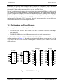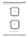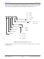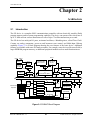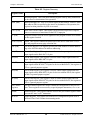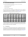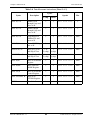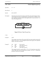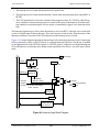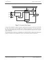
1
www.ubicom.com
™
Ubicom
SX Family
User’s Manual
SX User’s Manual Rev. 3.1
© 2000 Ubicom, Inc. All rights reserved.
www.ubicom.com
Revision History
REVISION
RELEASE DATE
SUMMARY OF CHANGES
2.0
February 11, 1999
2.01
June 14, 1999
Conyents the same as Rev 2.0 but removed the
last chapter (Device Programming)
2.1
May 19, 1999
Updated to reflect the new revision of the
SX18/20/28 AC devices (datecode Axyywwxx)
2.2
June 4, 1999
Deleted the recommended component values
associated with resonator/crystal oscillator. This
information is available in the datasheets.
3.0
January 21, 2000
Updated to reflect the latest revision of the
SX48/52BD (Production Part)
3.1
August 24, 2000
Updated to correct errata sheet items.
Updated to include SX48/52BD devices
©2000 Ubicom, Inc. All rights reserved. No warranty is provided and no liability is assumed by
Ubicom with respect to the accuracy of this documentation or the merchantability or fitness of the
product for a particular application. No license of any kind is conveyed by Ubicom with respect to its
intellectual property or that of others. All information in this document is subject to change without
notice.
Ubicom products are not authorized for use in life support systems or under conditions where failure
of the product would endanger the life or safety of the user, except when prior written approval is
obtained from Ubicom.
Ubicom™ and the Ubicom logo are trademarks of Ubicom, Inc.
Virtual Peripheral™ is a trademark of Ubicom, Inc.
I2C™ is a trademark of Philips Corporation
All other trademarks mentioned in this document are property of their respective companies.
Ubicom Inc., 1330 Charleston Road, Mountain View, CA 94043, USA
Telephone: +1 650 210 1500, Fax: +1 650 210 8715, Web site: www.ubicom.com,
E-mail: [email protected]
© 2000 Ubicom, Inc. All rights reserved.
SX User’s Manual Rev. 3.1
www.ubicom.com
Contents
Contents
Chapter 1
1.1
1.2
1.3
1.4
1.5
1.6
1.7
1.8
1.9
Overview
Introduction . . . . . . . . . . . . . . . . . . . . . . . . . . . . . . . . . . . . . . . . . . . . . . . . . . . . . . . . 11
Key Features . . . . . . . . . . . . . . . . . . . . . . . . . . . . . . . . . . . . . . . . . . . . . . . . . . . . . . . 11
Architecture . . . . . . . . . . . . . . . . . . . . . . . . . . . . . . . . . . . . . . . . . . . . . . . . . . . . . . . . 13
The Virtual Peripheral Concept . . . . . . . . . . . . . . . . . . . . . . . . . . . . . . . . . . . . . . . . . 13
The Communications Controller . . . . . . . . . . . . . . . . . . . . . . . . . . . . . . . . . . . . . . . . 14
Programming and Debugging Support . . . . . . . . . . . . . . . . . . . . . . . . . . . . . . . . . . . 14
Applications . . . . . . . . . . . . . . . . . . . . . . . . . . . . . . . . . . . . . . . . . . . . . . . . . . . . . . . . 14
Part Numbers and Pinout Diagrams . . . . . . . . . . . . . . . . . . . . . . . . . . . . . . . . . . . . . . 15
Pin Descriptions . . . . . . . . . . . . . . . . . . . . . . . . . . . . . . . . . . . . . . . . . . . . . . . . . . . . . 19
Chapter 2
2.1
2.2
2.3
Architecture
Introduction . . . . . . . . . . . . . . . . . . . . . . . . . . . . . . . . . . . . . . . . . . . . . . . . . . . . . . . . 21
Program Memory . . . . . . . . . . . . . . . . . . . . . . . . . . . . . . . . . . . . . . . . . . . . . . . . . . . . 22
Data Memory . . . . . . . . . . . . . . . . . . . . . . . . . . . . . . . . . . . . . . . . . . . . . . . . . . . . . . . 22
2.3.1
Banks . . . . . . . . . . . . . . . . . . . . . . . . . . . . . . . . . . . . . . . . . . . . . . . . . . . . 22
2.3.2
SX18/20/28AC and SX18/20/28AC75 Addressing Modes and
FSR Register . . . . . . . . . . . . . . . . . . . . . . . . . . . . . . . . . . . . . . . . . . . . . . . 23
2.3.3
SX48/52BD Addressing Modes and FSR Register . . . . . . . . . . . . . . . . . 25
2.3.4
Register Access Examples . . . . . . . . . . . . . . . . . . . . . . . . . . . . . . . . . . . . 28
Special-Function Registers . . . . . . . . . . . . . . . . . . . . . . . . . . . . . . . . . . . . . . . . . . . . 29
2.4.1
W (Working Register) . . . . . . . . . . . . . . . . . . . . . . . . . . . . . . . . . . . . . . . 31
2.4.2
INDF (Indirect through FSR) . . . . . . . . . . . . . . . . . . . . . . . . . . . . . . . . . 31
2.4.3
RTCC (Real-Time Clock/Counter) . . . . . . . . . . . . . . . . . . . . . . . . . . . . . 31
2.4.4
PC (Program Counter) . . . . . . . . . . . . . . . . . . . . . . . . . . . . . . . . . . . . . . . 31
2.4.5
STATUS (Status Register) . . . . . . . . . . . . . . . . . . . . . . . . . . . . . . . . . . . . 32
2.4.6
FSR (File Select Register) . . . . . . . . . . . . . . . . . . . . . . . . . . . . . . . . . . . . 34
2.4.7
RA through RE (Port Data Registers) . . . . . . . . . . . . . . . . . . . . . . . . . . . 34
2.4.8
Port Control Registers and MODE Register . . . . . . . . . . . . . . . . . . . . . . 34
2.4.9
OPTION (Device Option Register) . . . . . . . . . . . . . . . . . . . . . . . . . . . . . 37
Instruction Execution Pipeline . . . . . . . . . . . . . . . . . . . . . . . . . . . . . . . . . . . . . . . . . . 39
2.5.1
Clocking Modes . . . . . . . . . . . . . . . . . . . . . . . . . . . . . . . . . . . . . . . . . . . . 39
2.5.2
Pipeline Delays . . . . . . . . . . . . . . . . . . . . . . . . . . . . . . . . . . . . . . . . . . . . 40
2.5.3
Read-Modify-Write Considerations . . . . . . . . . . . . . . . . . . . . . . . . . . . . 40
Program Counter . . . . . . . . . . . . . . . . . . . . . . . . . . . . . . . . . . . . . . . . . . . . . . . . . . . . 41
2.6.1
Test and Skip . . . . . . . . . . . . . . . . . . . . . . . . . . . . . . . . . . . . . . . . . . . . . . 41
2.6.2
Jump Absolute . . . . . . . . . . . . . . . . . . . . . . . . . . . . . . . . . . . . . . . . . . . . . 41
2.6.3
Jump Indirect and Jump Relative . . . . . . . . . . . . . . . . . . . . . . . . . . . . . . . 42
2.6.4
Call . . . . . . . . . . . . . . . . . . . . . . . . . . . . . . . . . . . . . . . . . . . . . . . . . . . . . . 43
2.6.5
Return . . . . . . . . . . . . . . . . . . . . . . . . . . . . . . . . . . . . . . . . . . . . . . . . . . . . 44
Stack . . . . . . . . . . . . . . . . . . . . . . . . . . . . . . . . . . . . . . . . . . . . . . . . . . . . . . . . . . . . . . 45
2.4
2.5
2.6
2.7
© 2000 Ubicom, Inc. All rights reserved.
3
SX User’s Manual Rev. 3.1
Contents
www.ubicom.com
2.8
Device Configuration Options . . . . . . . . . . . . . . . . . . . . . . . . . . . . . . . . . . . . . . . . . . 47
Chapter 3
3.1
3.2
3.3
Instruction Set
Introduction . . . . . . . . . . . . . . . . . . . . . . . . . . . . . . . . . . . . . . . . . . . . . . . . . . . . . . . . 55
Instruction Operands . . . . . . . . . . . . . . . . . . . . . . . . . . . . . . . . . . . . . . . . . . . . . . . . . 55
Instruction Types . . . . . . . . . . . . . . . . . . . . . . . . . . . . . . . . . . . . . . . . . . . . . . . . . . . . 56
3.3.1
Logic Instructions . . . . . . . . . . . . . . . . . . . . . . . . . . . . . . . . . . . . . . . . . . 56
3.3.2
Arithmetic and Shift Instructions . . . . . . . . . . . . . . . . . . . . . . . . . . . . . . . 56
3.3.3
Bitwise Operation Instructions . . . . . . . . . . . . . . . . . . . . . . . . . . . . . . . . 57
3.3.4
Data Movement Instructions . . . . . . . . . . . . . . . . . . . . . . . . . . . . . . . . . . 57
3.3.5
Program Control Instructions . . . . . . . . . . . . . . . . . . . . . . . . . . . . . . . . . . 57
3.3.6
System Control Instructions . . . . . . . . . . . . . . . . . . . . . . . . . . . . . . . . . . . 59
Instruction Summary Tables . . . . . . . . . . . . . . . . . . . . . . . . . . . . . . . . . . . . . . . . . . . 59
Equivalent Assembler Mnemonics . . . . . . . . . . . . . . . . . . . . . . . . . . . . . . . . . . . . . . 64
Detailed Instruction Descriptions . . . . . . . . . . . . . . . . . . . . . . . . . . . . . . . . . . . . . . . 64
3.6.1
ADD fr,W
Add W to fr . . . . . . . . . . . . . . . . . . . . . . . . . . . . . 67
3.6.2
ADD W,fr
Add fr to W . . . . . . . . . . . . . . . . . . . . . . . . . . . . . 68
3.6.3
AND fr,W
AND of fr and W into fr . . . . . . . . . . . . . . . . . . . 69
3.6.4
AND W,fr
AND of W and fr into W . . . . . . . . . . . . . . . . . . . 70
3.6.5
AND W,#lit
AND of W and Literal into W . . . . . . . . . . . . . . . 71
3.6.6
BANK addr8
Load Bank Number into FSR(6:4) . . . . . . . . . . . . 72
3.6.7
CALL addr8
Call Subroutine . . . . . . . . . . . . . . . . . . . . . . . . . . 74
3.6.8
CLR fr
Clear fr . . . . . . . . . . . . . . . . . . . . . . . . . . . . . . . . . 76
3.6.9
CLR W
Clear W . . . . . . . . . . . . . . . . . . . . . . . . . . . . . . . . 77
3.6.10
CLR !WDT
Clear Watchdog Timer . . . . . . . . . . . . . . . . . . . . . 78
3.6.11
CLRB fr.bit
Clear Bit in fr . . . . . . . . . . . . . . . . . . . . . . . . . . . . 79
3.6.12
DEC fr
Decrement fr . . . . . . . . . . . . . . . . . . . . . . . . . . . . 80
3.6.13
DECSZ fr
Decrement fr and Skip if Zero . . . . . . . . . . . . . . . 81
3.6.14
INC fr
Increment fr . . . . . . . . . . . . . . . . . . . . . . . . . . . . . 82
3.6.15
INCSZ fr
Increment fr and Skip if Zero . . . . . . . . . . . . . . . 83
3.6.16
IREAD
Read Word from Instruction Memory . . . . . . . . . 84
3.6.17
JMP addr9
Jump to Address . . . . . . . . . . . . . . . . . . . . . . . . . . 86
3.6.18
MOV fr,W
Move W to fr . . . . . . . . . . . . . . . . . . . . . . . . . . . . 87
3.6.19
MOV M,#lit
Move Literal to MODE Register . . . . . . . . . . . . . 88
3.6.20
MOV M,W
Move W to MODE Register . . . . . . . . . . . . . . . . 89
3.6.21
MOV !OPTION,W Move W to OPTION Register . . . . . . . . . . . . . . . 90
3.6.22
MOV !rx,W
Move Data Between W and Control Register . . . 91
3.6.23
MOV W,fr
Move fr to W . . . . . . . . . . . . . . . . . . . . . . . . . . . . 93
3.6.24
MOV W,/fr
Move Complement of fr to W . . . . . . . . . . . . . . . 94
3.6.25
MOV W,fr-W
Move (fr-W) to W . . . . . . . . . . . . . . . . . . . . . . . . 95
3.6.26
MOV W,--fr
Move (fr-1) to W . . . . . . . . . . . . . . . . . . . . . . . . . 96
3.6.27
MOV W,++fr
Move (fr+1) to W . . . . . . . . . . . . . . . . . . . . . . . . . 97
3.6.28
MOV W,<<fr
Rotate fr Left through Carry and Move to W . . . 98
3.6.29
MOV W,>>fr
Rotate fr Right through Carry and Move to W . . 99
3.6.30
MOV W,<>fr
Swap High/Low Nibbles of fr and Move to W . 100
3.6.31
MOV W,#lit
Move Literal to W . . . . . . . . . . . . . . . . . . . . . . . 101
3.4
3.5
3.6
SX User’s Manual Rev. 3.1
4
© 2000 Ubicom, Inc. All rights reserved.
www.ubicom.com
Chapter 4
4.1
4.2
4.3
4.4
4.5
Contents
3.6.32
3.6.33
3.6.34
3.6.35
3.6.36
3.6.37
3.6.38
3.6.39
3.6.40
3.6.41
3.6.42
3.6.43
MOV W,M
MOVSZ W, --fr
MOVSZ W, ++fr
NOP
NOT fr
OR fr,W
OR W,fr
OR W,#lit
PAGE addr12
RET
RETI
RETIW
3.6.44
3.6.45
3.6.46
3.6.47
3.6.48
3.6.49
3.6.50
3.6.51
3.6.52
3.6.53
3.6.54
3.6.55
3.6.56
3.6.57
RETP
RETW lit
RL fr
RR fr
SB fr.bit
SETB fr.bit
SLEEP
SNB fr.bit
SUB fr,W
SWAP fr
TEST fr
XOR fr,W
XOR W,fr
XOR W,#lit
Move MODE Register to W . . . . . . . . . . . . . . . 102
Move (fr-1) to W and Skip if Zero . . . . . . . . . . 103
Move (fr+1) to W and Skip if Zero . . . . . . . . . . 104
No Operation . . . . . . . . . . . . . . . . . . . . . . . . . . . 105
Complement of fr into fr . . . . . . . . . . . . . . . . . . 106
OR of fr and W into fr . . . . . . . . . . . . . . . . . . . . 107
OR of W and fr into W . . . . . . . . . . . . . . . . . . . 108
OR of W and Literal into W . . . . . . . . . . . . . . . 109
Load Page Number into STATUS(7:5) . . . . . . . 110
Return from Subroutine . . . . . . . . . . . . . . . . . . . 111
Return from Interrupt . . . . . . . . . . . . . . . . . . . . . 112
Return from Interrupt and Adjust RTCC with
W . . . . . . . . . . . . . . . . . . . . . . . . . . . . . . . . . . . . 113
Return from Subroutine Across Page Boundary 114
Return from Subroutine with Literal in W . . . . . 115
Rotate fr Left through Carry . . . . . . . . . . . . . . . 116
Rotate fr Right through Carry . . . . . . . . . . . . . . 117
Test Bit in fr and Skip if Set . . . . . . . . . . . . . . . 118
Set Bit in fr . . . . . . . . . . . . . . . . . . . . . . . . . . . . . 119
Power Down Mode . . . . . . . . . . . . . . . . . . . . . . 120
Test Bit in fr and Skip if Clear . . . . . . . . . . . . . . 121
Subtract W from fr . . . . . . . . . . . . . . . . . . . . . . . 122
Swap High/Low Nibbles of fr . . . . . . . . . . . . . . 124
Test fr for Zero . . . . . . . . . . . . . . . . . . . . . . . . . . 125
XOR of fr and W into fr . . . . . . . . . . . . . . . . . . . 126
XOR of W and fr into W . . . . . . . . . . . . . . . . . . 127
XOR of W and Literal into W . . . . . . . . . . . . . . 128
Clocking, Power Down, and Reset
Introduction . . . . . . . . . . . . . . . . . . . . . . . . . . . . . . . . . . . . . . . . . . . . . . . . . . . . . . . 129
Clocking Options . . . . . . . . . . . . . . . . . . . . . . . . . . . . . . . . . . . . . . . . . . . . . . . . . . . 129
4.2.1
Clock/Instruction Rate Option (Compatible or Turbo Mode) . . . . . . . . 129
4.2.2
Internal RC Oscillator . . . . . . . . . . . . . . . . . . . . . . . . . . . . . . . . . . . . . . 130
4.2.3
External RC Oscillator . . . . . . . . . . . . . . . . . . . . . . . . . . . . . . . . . . . . . . 130
4.2.4
External Crystal/Resonator (XT, LP, or HS Mode) . . . . . . . . . . . . . . . . 131
4.2.5
External Clock Signal . . . . . . . . . . . . . . . . . . . . . . . . . . . . . . . . . . . . . . 132
Power Down Mode . . . . . . . . . . . . . . . . . . . . . . . . . . . . . . . . . . . . . . . . . . . . . . . . . 133
4.3.1
Entering the Power Down Mode . . . . . . . . . . . . . . . . . . . . . . . . . . . . . . 133
4.3.2
Waking Up from the Power Down Mode . . . . . . . . . . . . . . . . . . . . . . . 134
Multi-Input Wakeup/Interrupt . . . . . . . . . . . . . . . . . . . . . . . . . . . . . . . . . . . . . . . . . 134
4.4.1
Port B Configuration for Multi-Input Wakeup/Interrupt . . . . . . . . . . . . 134
4.4.2
Reading and Writing the Wakeup Pending Bits . . . . . . . . . . . . . . . . . . 137
Reset . . . . . . . . . . . . . . . . . . . . . . . . . . . . . . . . . . . . . . . . . . . . . . . . . . . . . . . . . . . . . 138
4.5.1
Register States Upon Different Resets . . . . . . . . . . . . . . . . . . . . . . . . . . 138
4.5.2
Power-On Reset . . . . . . . . . . . . . . . . . . . . . . . . . . . . . . . . . . . . . . . . . . . 140
4.5.3
Wakeup from the Power Down Mode . . . . . . . . . . . . . . . . . . . . . . . . . . 141
4.5.4
Brown-Out Reset . . . . . . . . . . . . . . . . . . . . . . . . . . . . . . . . . . . . . . . . . . 142
© 2000 Ubicom, Inc. All rights reserved.
5
SX User’s Manual Rev. 3.1
Contents
www.ubicom.com
4.5.5
4.5.6
Watchdog Timeout . . . . . . . . . . . . . . . . . . . . . . . . . . . . . . . . . . . . . . . . 142
MCLR Input Signal (Master Clear Reset) . . . . . . . . . . . . . . . . . . . . . . . 142
Chapter 5
5.1
5.2
5.3
Input/Output Ports
Introduction . . . . . . . . . . . . . . . . . . . . . . . . . . . . . . . . . . . . . . . . . . . . . . . . . . . . . . . 143
Reading and Writing the Ports . . . . . . . . . . . . . . . . . . . . . . . . . . . . . . . . . . . . . . . . . 143
Port Configuration . . . . . . . . . . . . . . . . . . . . . . . . . . . . . . . . . . . . . . . . . . . . . . . . . . 144
5.3.1
Accessing the Port Control Registers . . . . . . . . . . . . . . . . . . . . . . . . . . 145
5.3.2
MODE Register . . . . . . . . . . . . . . . . . . . . . . . . . . . . . . . . . . . . . . . . . . . 145
5.3.3
Port Configuration Example . . . . . . . . . . . . . . . . . . . . . . . . . . . . . . . . . 147
5.3.4
Port Configuration Registers . . . . . . . . . . . . . . . . . . . . . . . . . . . . . . . . . 147
5.3.5
Port Configuration Upon Reset . . . . . . . . . . . . . . . . . . . . . . . . . . . . . . . 149
5.3.6
Port Block Diagram . . . . . . . . . . . . . . . . . . . . . . . . . . . . . . . . . . . . . . . . 149
Chapter 6
6.1
6.2
Timers and Interrupts
Introduction . . . . . . . . . . . . . . . . . . . . . . . . . . . . . . . . . . . . . . . . . . . . . . . . . . . . . . . 151
Real-Time Clock/Counter . . . . . . . . . . . . . . . . . . . . . . . . . . . . . . . . . . . . . . . . . . . . 151
6.2.1
Prescaler Register . . . . . . . . . . . . . . . . . . . . . . . . . . . . . . . . . . . . . . . . . 152
6.2.2
Maximum Count . . . . . . . . . . . . . . . . . . . . . . . . . . . . . . . . . . . . . . . . . . 152
6.2.3
RTCC Operation as a Real-Time Clock or Timer . . . . . . . . . . . . . . . . . 153
6.2.4
RTCC Operation as an Event Counter . . . . . . . . . . . . . . . . . . . . . . . . . . 153
6.2.5
RTCC Overflow Interrupts . . . . . . . . . . . . . . . . . . . . . . . . . . . . . . . . . . 153
Watchdog Timer . . . . . . . . . . . . . . . . . . . . . . . . . . . . . . . . . . . . . . . . . . . . . . . . . . . 154
6.3.1
Watchdog Timeout Period . . . . . . . . . . . . . . . . . . . . . . . . . . . . . . . . . . . 154
6.3.2
Watchdog Operation in the Power Down Mode . . . . . . . . . . . . . . . . . . 155
Interrupts . . . . . . . . . . . . . . . . . . . . . . . . . . . . . . . . . . . . . . . . . . . . . . . . . . . . . . . . . 155
6.4.1
Single-Level Interrupt Operation . . . . . . . . . . . . . . . . . . . . . . . . . . . . . . 156
6.4.2
Interrupt Sequence . . . . . . . . . . . . . . . . . . . . . . . . . . . . . . . . . . . . . . . . . 156
6.4.3
RTCC Interrupts . . . . . . . . . . . . . . . . . . . . . . . . . . . . . . . . . . . . . . . . . . 157
6.4.4
Port B Interrupts . . . . . . . . . . . . . . . . . . . . . . . . . . . . . . . . . . . . . . . . . . . 157
6.4.5
Device-Specific Interrupts . . . . . . . . . . . . . . . . . . . . . . . . . . . . . . . . . . . 158
6.4.6
Return-from-Interrupt Instructions . . . . . . . . . . . . . . . . . . . . . . . . . . . . 159
6.4.7
Interrupt Example . . . . . . . . . . . . . . . . . . . . . . . . . . . . . . . . . . . . . . . . . 159
6.3
6.4
Chapter 7
7.1
7.2
7.3
Analog Comparator
Introduction . . . . . . . . . . . . . . . . . . . . . . . . . . . . . . . . . . . . . . . . . . . . . . . . . . . . . . . 161
Comparator Enable/Status Register (CMP_B) . . . . . . . . . . . . . . . . . . . . . . . . . . . . 161
7.2.1
Accessing the CMP_B Register . . . . . . . . . . . . . . . . . . . . . . . . . . . . . . . 162
Comparator Operation . . . . . . . . . . . . . . . . . . . . . . . . . . . . . . . . . . . . . . . . . . . . . . . 162
SX User’s Manual Rev. 3.1
6
© 2000 Ubicom, Inc. All rights reserved.
www.ubicom.com
Chapter 8
8.1
8.2
8.3
8.4
Contents
Multi-Function Timers
Introduction . . . . . . . . . . . . . . . . . . . . . . . . . . . . . . . . . . . . . . . . . . . . . . . . . . . . . . . 165
Timer Operating Modes . . . . . . . . . . . . . . . . . . . . . . . . . . . . . . . . . . . . . . . . . . . . . . 166
8.2.1
PWM Mode . . . . . . . . . . . . . . . . . . . . . . . . . . . . . . . . . . . . . . . . . . . . . . 166
8.2.2
Software Timer Mode . . . . . . . . . . . . . . . . . . . . . . . . . . . . . . . . . . . . . . 166
8.2.3
External Event Mode . . . . . . . . . . . . . . . . . . . . . . . . . . . . . . . . . . . . . . . 167
8.2.4
Capture/Compare Mode . . . . . . . . . . . . . . . . . . . . . . . . . . . . . . . . . . . . . 167
Timer Pin Assignments . . . . . . . . . . . . . . . . . . . . . . . . . . . . . . . . . . . . . . . . . . . . . . 168
Timer Control Registers . . . . . . . . . . . . . . . . . . . . . . . . . . . . . . . . . . . . . . . . . . . . . . 168
8.4.1
Timer T1 Control A Register (T1CNTA) . . . . . . . . . . . . . . . . . . . . . . . 169
8.4.2
Timer T1 Control B Register (T1CNTB) . . . . . . . . . . . . . . . . . . . . . . . 170
8.4.3
Timer T2 Control A Register (T2CNTA) . . . . . . . . . . . . . . . . . . . . . . . 171
8.4.4
Timer T2 Control B Register (T2CNTB) . . . . . . . . . . . . . . . . . . . . . . . 172
© 2000 Ubicom, Inc. All rights reserved.
7
SX User’s Manual Rev. 3.1
www.ubicom.com
Contents
List of Figures
Figure 1-1
Figure 1-2
Figure 1-3
Figure 2-1
Figure 2-2
Figure 2-3
Figure 2-4
Figure 2-5
Figure 2-6
Figure 2-7
Figure 3-1
Figure 3-2
Figure 3-3
Figure 3-4
Figure 3-5
Figure 4-1
Figure 4-2
Figure 4-3
Figure 4-4
Figure 4-5
Figure 4-6
Figure 4-7
Figure 4-8
Figure 4-9
Figure 5-1
Figure 6-1
Figure 6-2
Figure 7-1
Figure 8-1
SX18/20/28 Pin Assignments . . . . . . . . . . . . . . . . . . . . . . . . . . . . . . . . . . . . . . . . 15
SX48/52BD Pin Assignments. . . . . . . . . . . . . . . . . . . . . . . . . . . . . . . . . . . . . . . . 16
Part Numbering Reference Guide. . . . . . . . . . . . . . . . . . . . . . . . . . . . . . . . . . . . . 18
SX28AC Block Diagram . . . . . . . . . . . . . . . . . . . . . . . . . . . . . . . . . . . . . . . . . . . 21
Register Access Modes . . . . . . . . . . . . . . . . . . . . . . . . . . . . . . . . . . . . . . . . . . . . . 27
Program Counter Loading for Jump Instruction. . . . . . . . . . . . . . . . . . . . . . . . . . 43
Program Counter Loading for Call Instruction. . . . . . . . . . . . . . . . . . . . . . . . . . . 43
Stack Operation for a “Call” Instruction. . . . . . . . . . . . . . . . . . . . . . . . . . . . . . . . 46
Stack Operation for a “Return” Instruction . . . . . . . . . . . . . . . . . . . . . . . . . . . . . 46
Device Configuration Register Formats . . . . . . . . . . . . . . . . . . . . . . . . . . . . . . . . 48
Program Counter Loading for Call Instruction. . . . . . . . . . . . . . . . . . . . . . . . . . . 84
Rotate fr Left Through Carry into W . . . . . . . . . . . . . . . . . . . . . . . . . . . . . . . . . . 98
Rotate fr Right Through Carry into W . . . . . . . . . . . . . . . . . . . . . . . . . . . . . . . . . 99
Rotate fr Left Through Carry . . . . . . . . . . . . . . . . . . . . . . . . . . . . . . . . . . . . . . . 116
Rotate fr Right Through Carry . . . . . . . . . . . . . . . . . . . . . . . . . . . . . . . . . . . . . . 117
External RC Oscillator Connections. . . . . . . . . . . . . . . . . . . . . . . . . . . . . . . . . . 131
Crystal or Ceramic Resonator Connections . . . . . . . . . . . . . . . . . . . . . . . . . . . . 132
External Clock Signal Connection . . . . . . . . . . . . . . . . . . . . . . . . . . . . . . . . . . . 133
Multi-Input Wakeup/Interrupt Block Diagram. . . . . . . . . . . . . . . . . . . . . . . . . . 135
On-Chip Reset Circuit Block Diagram . . . . . . . . . . . . . . . . . . . . . . . . . . . . . . . . 138
Power-On Reset Timing, Fast VDD Rise Time . . . . . . . . . . . . . . . . . . . . . . . . . 140
Power-On Reset Timing, VDD Rise Time Too Slow . . . . . . . . . . . . . . . . . . . . 141
External Power-On MCLR Signal . . . . . . . . . . . . . . . . . . . . . . . . . . . . . . . . . . . 141
Power-On Reset Timing, Separate MCLR Signal . . . . . . . . . . . . . . . . . . . . . . . 141
Port B Pin Block Diagram . . . . . . . . . . . . . . . . . . . . . . . . . . . . . . . . . . . . . . . . . 150
RTCC Block Diagram . . . . . . . . . . . . . . . . . . . . . . . . . . . . . . . . . . . . . . . . . . . . 152
Interrupt Logic Block Diagram. . . . . . . . . . . . . . . . . . . . . . . . . . . . . . . . . . . . . . 158
Comparator Block Diagram . . . . . . . . . . . . . . . . . . . . . . . . . . . . . . . . . . . . . . . . 163
Multi-Function Timer Block Diagram . . . . . . . . . . . . . . . . . . . . . . . . . . . . . . . . 165
© 2000 Ubicom, Inc. All rights reserved.
8
SX User’s Manual Rev. 3.1
www.ubicom.com
Contents
List of Tables
Table 1-1
Table 1-2
Table 2-1
Table 2-2
Table 2-3
Table 2-4
Table 2-5
Table 2-6
Table 2-7
Table 2-8
Table 2-9
Table 2-10
Table 2-11
Table 2-12
Table 3-1
Table 3-2
Table 3-3
Table 3-4
Table 3-5
Table 3-6
Table 3-7
Table 3-8
Table 4-1
Table 5-1
Table 5-2
Table 6-1
Table 8-1
Table 8-2
Table 8-3
Table 8-4
Table 8-5
Device Package Names ...............................................................................................17
Pin Descriptions ..........................................................................................................20
SX18/20/28AC and SX18/20/28AC75 RAM Register Map ......................................24
Register Summary .......................................................................................................30
STATUS Register Bits ................................................................................................32
MODE Register Settings for SX18/20/28AC and SX18/20/28AC75 ........................35
MODE Register Settings for SX48/52BD ..................................................................36
Prescaler Divide-By Factors .......................................................................................38
Pipeline Execution Sequence ......................................................................................39
Return-from-Subroutine/Interrupt Instructions ...........................................................45
FUSE Word Register Configuration Bits for SX18/20/28AC ....................................49
FUSEX Word Register Configuration Bits for SX18/20/28AC &
SX18/20/28AC75 ........................................................................................................51
FUSE Word Configuration Bits for SX48/52BD .......................................................52
FUSEX Word Register Configuration Bits for SX48/52BD ......................................54
Logic Instructions .......................................................................................................60
Arithmetic and Shift Instructions ................................................................................60
Bitwise Operation Instructions ...................................................................................61
Data Movement Instructions .......................................................................................61
Program Control Instructions ......................................................................................63
System Control Instructions ........................................................................................63
Equivalent Assembler Mnemonics .............................................................................64
Key to Abbreviations and Symbols ............................................................................66
Register States Upon Different Resets ......................................................................139
MODE Register Settings for SX18/20/28AC and SX18/20/28AC75 ......................146
MODE Register Settings for SX48/52BD ................................................................146
Watchdog Timeout Settings ......................................................................................155
Timer T1/T2 Pin Assignments ..................................................................................168
T1CNTA Register Bits .............................................................................................169
T1CNTB Register Bits ..............................................................................................170
T2CNTA Register Bits .............................................................................................171
T2CNTB Register Bits ..............................................................................................172
© 2000 Ubicom, Inc. All rights reserved.
9
SX User’s Manual Rev. 3.1
Contents
SX User’s Manual Rev. 3.1
www.ubicom.com
10
© 2000 Ubicom, Inc. All rights reserved.
www.ubicom.com
Chapter 1
Overview
1.1
Introduction
The Ubicom SX family of configurable communications controllers are fabricated in an advanced
CMOS process technology. The advanced process, combined with a RISC-based architecture, allows
high-speed computation, flexible I/O control, and efficient data manipulation. Throughput is enhanced
by operating the device at frequencies up to 100 MHz and by optimizing the instruction set to include
mostly single-cycle instructions. In addition, the SX architecture is deterministic and totally
reprogramable. The unique combination of these characteristics enables the device to implement realtime functions as software modules (Virtual PeripheralTM) to replace traditional hardware functions.
On-chip core functions include a general-purpose 8-bit timer with prescaler, an analog comparator, a
brown-out detector, a watchdog timer, a power-save mode with multi-source wakeup capability, an
internal R/C oscillator, user-selectable clock modes, and high-current outputs. Additional features are
provided by individual members of the SX family according to the system requirements, such as PWM
timers and additional I/O ports.
1.2
Key Features
50/75/100 MIPS Performance
• DC - 100 MHz operation
• 10 ns instruction cycle, 30 ns internal interrupt response at 100 MHz
• 1 instruction per clock (branches 3)
EE/FLASH Program Memory and SRAM Data Memory
• Access time of < 10 ns provides single cycle access
• EE/Flash rated for > 10,000 rewrite cycles
• SX18/20/28AC and SX18/20/28AC75:
– 2048 words of EE/Flash program memory
– 136 bytes of SRAM data memory
• SX48/52BD:
– 4096 words of EE/Flash program memory
– 262 bytes of SRAM data memory
SX User’s Manual Rev. 3.1
11
© 2000 Ubicom, Inc. All rights reserved.
Chapter 1 Overview
www.ubicom.com
CPU Features
• Compact instruction set
• All instructions are single cycle except branch
• Eight-level push/pop hardware stack for subroutine linkage
• Fast table lookup capability through run-time readable code (IREAD instruction)
• Predictable program execution flow for hard real-time applications
Fast and Deterministic Interrupt
• Jitter-free 3-cycle internal interrupt response
• Hardware context save/restore of key resources such as PC, W, STATUS, and FSR within the 3cycle interrupt response time
• External wakeup/interrupt capability on Port B (8 pins)
Flexible I/O
• All pins individually programmable as I/O
• Inputs are TTL or CMOS level selectable
• All pins have selectable internal pull-ups
• Selectable Schmitt Trigger inputs on Ports B, C, D, and E
• All outputs capable of sourcing/sinking 30 mA
• Port A outputs have symmetrical drive
• Analog comparator support on Port B (RB0 OUT, RB1 IN-, RB2 IN+)
• I/O operation synchronous to the oscillator clock (user selectable)
Hardware Peripheral Features
• Two 16-bit timers with 8-bit prescalers supporting (SX48/52BD devices only):
–
–
–
–
•
•
•
•
•
•
•
Software Timer mode
PWM mode
Simultaneous PWM/Capture mode
External Event mode
One 8-bit Real Time Clock/Counter (RTCC) with programable 8-bit prescaler
Watchdog Timer (shares the RTCC prescaler)
Analog comparator
Brown-out detector
Multi-Input Wakeup logic on 8 pins
Internal RC oscillator with configurable rate from 31.25 KHz to 4 MHz
Power-On-Reset
Packages
• SX18/2028AC and SX18/20/28AC75: 18pin SO/DIP, 20-pin SSOP, 28-pin SO/DIP
• SX48/52BD family: 48-pin Tiny PQFP, and 52-pin PQFP
• SX52BD75: 52-pin PQFP
• SX52BD100: 52-pin PQFP
SX User’s Manual Rev. 3.1
12
© 2000 Ubicom, Inc. All rights reserved.
www.ubicom.com
Chapter 1 Overview
Programming and Debugging Support
• On- chip in-system programming support through serial or parallel interface
• In-system serial programming via oscillator pins
• On-chip in-system debugging support logic
• Real-time emulation, full program debug, and integrated development environment offered by third
party tool vendors
Software Support
• Library of off-the-shelf Virtual Peripheral modules
• Examples of Virtual Peripheral integration
• Evaluation Kits for communication intensive applications
1.3
Architecture
The SX devices use a modified Harvard architecture. This architecture uses two separate memories
with separate address buses, one for the program and one for data, while allowing transfer of data
from program memory to SRAM. This ability allows accessing data tables from program memory.
The advantage of this architecture is that instruction fetch and memory transfers can be overlapped
with a multi-stage pipeline, which means the next instruction can be fetched from program memory
while the current instruction is being executed using data from the data memory.
Ubicom has developed a revolutionary RISC-based architecture and memory design techniques that
is 20 times faster than conventional MCUs, deterministic, jitter free, and totally reprogramable.
The SX family implements a four-stage pipeline (fetch, decode, execute, and write back), which
results in execution of one instruction per clock cycle. At the operating frequency of 100 MHz,
instructions are executed at the rate of one per 10-ns clock cycle.
1.4
The Virtual Peripheral Concept
Virtual Peripheral concept enables the “software system on a chip” approach. Virtual Peripheral, a
software module that replaces a traditional hardware peripheral, takes advantage of the Ubicom architecture’s high performance and deterministic nature to produce same results as the hardware peripheral with much greater flexibility.
The speed and flexibility of the Ubicom architecture complemented with the availability of the Virtual Peripheral library, simultaneously address a wide range of engineering and product development
concerns. They decrease the product development cycle dramatically, shortening time to production
to as little as a few days.
Ubicom’s time-saving Virtual Peripheral library gives the system designers a choice of ready-made
solutions, or a head start on developing their own peripherals. So, with Virtual Peripheral modules
handling established functions, design engineers can concentrate on adding value to other areas of the
application.
The concept of Virtual Peripheral combined with in-system re-programmability provides a powerful
development platform ideal for the communications industry because of the numerous and rapidly
evolving standards and protocols.
© 2000 Ubicom, Inc. All rights reserved.
13
SX User’s Manual Rev. 3.1
Chapter 1 Overview
www.ubicom.com
Overall, the concept of Virtual Peripheral provides benefits such as using a more simple device,
reduced component count, fast time to production, increased flexibility in design, customization to
your application, and ultimately overall system cost reduction.
Some examples of Virtual Peripheral modules are:
• Communication interfaces such as I2C™, Microwire/Plus™ , SPI, IrDA stack, UART, and Modem
functions
• Internet Connectivity protocols such as UDP, TCP/IP stack, HTTP, SMTP, POP3
• Frequency generation and measurement
• PPM/PWM generation
• Delta/Sigma ADC
• DTMF generation/detection
• PSK/FSK generation/detection
• FFT/DFT based algorithms
1.5
The Communications Controller
The combination of the Ubicom hardware architecture and the Virtual Peripheral concept create a
powerful, creative platform for the communications design communities: SX communications controller. Its high processing power, re-cofigurability, cost-effectiveness, and overall design freedom
give the designer the power to build products for the future with the confidence of knowing that they
can keep up with innovation in standards and other areas.
1.6
Programming and Debugging Support
The SX devices are currently supported by third party tool vendors. On-board in-system debug capabilities have been added, allowing tools to provide an integrated development environment including
editor, macro assembler, debugger, and programmer. Un-obtrusive in-system programming is provided through the OSC pins. For emulation purposes, there is no need for a bond-out chip, so the user
does not have to worry about the potential variations in electrical characteristics of a bond-out chip
and the actual chip used in the target application. The user can test and revise the fully debugged code
in the actual SX, in the actual application, and get to production much faster.
1.7
Applications
Emerging applications and advances in existing ones require higher performance while maintaining
low cost and fast time-to-production.
The SX device provides solutions for many familiar applications such as process controllers, electronic appliances/tools, security/monitoring systems, consumer automotive, sound generation, motor
control, and personal communication devices. In addition, the device is suitable for applications that
require DSP-like capabilities, such as closed-loop servo control (digital filters), digital answering
machines, voice notation, interactive toys, and magnetic-stripe readers.
SX User’s Manual Rev. 3.1
14
© 2000 Ubicom, Inc. All rights reserved.
www.ubicom.com
Chapter 1 Overview
Furthermore, the growing Virtual Peripheral library features new components, such as the Internet
Protocol stack, and communication interfaces, that allow design engineers to embed Internet connectivity into all of their products at extremely low cost and very little effort.
Ubicom’s complete network connectivity protocol stack implementation (SX-Stack), enables singlechip Web servers and E-mail appliances in embedded applications. The implementation includes the
physical layer interface with the TCP/IP network connectivity protocols, enabling system designers to
produce cost-effective embedded Internet devices without external physical access or a gateway PC.
The hardware platform for SX-Stack is the SX52BD communications controller. The device allows
implementation of the entire TCP/IP protocols, physical interface, and other relevant high-speed
communication interfaces as Virtual Peripheral modules.
1.8
Part Numbers and Pinout Diagrams
This user’s guide describes the following Ubicom SX devices:
•
SX18AC/SX20AC/ SX28AC and SX18AC75/SX20AC75/SX28AC75 devices (with 2K program memories)
•
SX48BD/SX52BD devices (with 4K program memories and multi-function timers)
The SX18AC/20AC/28AC and SX18AC75/SX20AC75/SX28AC75 devices are available in the pin
configurations shown in Figure 1-1. These devices are functionally the same except that the 18-pin and
20-pin devices do not have the port pins RC0 through RC7. Therefore, Port C cannot be used in the
smaller packages.
SX 28-PIN
SX 20-PIN
SX 18-PIN
RA2
RA3
RTCC
MCLR
Vss
RB0
RB1
RB2
RB3
1
2
3
4
5
6
7
8
9
18
17
16
15
14
13
12
11
10
RA2
RA1
RA3
RA0 RTCC
OSC1 MCLR
OSC2
Vss
Vdd
Vss
RB7
RB0
RB6
RB1
RB5
RB2
RB4
RB3
DIP/SOIC
1
2
3
4
5
6
7
8
9
10
20
19
18
17
16
15
14
13
12
11
SSOP
RTCC
Vdd
RA1
n.c.
RA0
Vss
OSC1
n.c.
OSC2
RA0
Vdd
RA1
Vdd
RA2
RB7
RA3
RB6
RB0
RB5
RB1
RB4
RB2
RB3
RB4
1
2
3
4
5
6
7
8
9
10
11
12
13
14
28
27
26
25
24
23
22
21
20
19
18
17
16
15
SX 28-PIN
MCLR
Vss
OSC1 RTCC
OSC2
Vdd
RC7
Vdd
RC6
RA0
RC5
RA1
RC4
RA2
RC3
RA3
RC2
RB0
RC1
RB1
RB2
RC0
RB3
RB7
RB4
RB6
Vss
RB5
DIP/SOIC
1
2
3
4
5
6
7
8
9
10
11
12
13
14
28
27
26
25
24
23
22
21
20
19
18
17
16
15
MCLR
OSC1
OSC2
RC7
RC6
RC5
RC4
RC3
RC2
RC1
RC0
RB7
RB6
RB5
SSOP
Figure 1-1 SX18/20/28 Pin Assignments
© 2000 Ubicom, Inc. All rights reserved.
15
SX User’s Manual Rev. 3.1
Chapter 1 Overview
www.ubicom.com
_
_
_
_
_
_
_
_
_
_
_
_
RTCC
Vss
Vdd
RE7
RE6
RE5
RE4
RE3
RE2
RE1
RE0
RD7
The SX48/52BD devices are available in the pin configurations shown in Figure 1-2. These devices
are functionally the same except that the 48-pin device does not have the port pins RA4 through RA7.
Therefore, the upper four pins of Port A are not available in the smaller package.
48 47 46 45 44 43 42 41 40 39 38 37
_
MCLR
_
OSC1
_
OSC2
_
Vdd
_
Vss
_
RA0
_
RA1
_
RA2
_
RA3
_
RB0
_
RB1
RB2 _
1
2
3
4
5
6
7
8
9
10
11
12
48 - PIN
TQFP
36
35
34
33
32
31
30
29
28
27
26
25
_
_
_
_
_
_
_
_
_
_
_
_
RD6
RD5
RD4
Vss
Vdd
RD3
RD2
RD1
RD0
RC7
RC6
RC5
_
_
_
_
_
_
_
_
_
_
_
_
_
RD7
RD6
RD5
RD4
Vss
Vdd
RD3
RD2
RD1
RD0
RC7
RC6
RC5
RB3
RB4
RB5
RB6
RB7
Vdd
Vss
RC0
RC1
RC2
RC3
RC4
_
_
_
_
_
_
_
_
_
_
_
_
13 14 15 16 17 18 19 20 21 22 23 24
_
_
_
_
_
_
_
_
_
_
_
_
_
RA5
RA4
RTCC
Vss
Vdd
RE7
RE6
RE5
RE4
RE3
RE2
RE1
RE0
Top View
_
_
_
_
_
_
_
_
_
_
_
_
_
52 51 50 49 48 47 46 45 44 43 42 41 40
1
39
2
38
3
37
4
36
5
35
6
34
52 - PIN
PQFP
7
33
8
32
9
31
10
30
11
29
12
28
13
27
14 15 16 17 18 19 20 21 22 23 24 25 26
RB2
RB3
RB4
RB5
RB6
RB7
Vdd
Vss
RC0
RC1
RC2
RC3
RC4
_
_
_
_
_
_
_
_
_
_
_
_
_
RA6
RA7
MCLR
OSC1
OSC2
Vdd
Vss
RA0
RA1
RA2
RA3
RB0
RB1
Top View
Figure 1-2 SX48/52BD Pin Assignments
SX User’s Manual Rev. 3.1
16
© 2000 Ubicom, Inc. All rights reserved.
www.ubicom.com
Chapter 1 Overview
Table 1-1 is a list of the available SX device packages and the corresponding number of pins, number
of I/O pins, program (flash) memory size, and general-purpose RAM size. Use this table as a guide for
ordering the parts that fit your requirements.
Table 1-1 Device Package Names
Pins
I/O
Operating
Frequency (MHz)
EE/Flash
(Words)
RAM
(Bytes)
Operating
Temp. (°C)
SX18AC/SO
SX18AC-I/SO
SX18AC75/SO
18
18
18
12
12
12
50
50
75
2K
2K
2K
136
136
136
0°C to +70°C
-40°C to +85°C
0°C to +70°C
SX18AC/DP
SX18AC-I/DP
SX18AC75/DP
18
18
18
12
12
12
50
50
75
2K
2K
2K
136
136
136
0°C to +70°C
-40°C to +85°C
0°C to +70°C
SX20AC/SS
SX20AC-I/SS
SX20AC75/SS
20
20
20
12
12
12
50
50
75
2K
2K
2K
136
136
136
0°C to +70°C
-40°C to +85°C
0°C to +70°C
SX28AC/SO
SX28AC-I/SO
SX28AC75/SO
28
28
28
20
20
20
50
50
75
2K
2K
2K
136
136
136
0°C to +70°C
-40°C to +85°C
0°C to +70°C
SX28AC/DP
SX28AC-I/DP
SX28AC75/DP
28
28
28
20
20
20
50
50
75
2K
2K
2K
136
136
136
0°C to +70°C
-40°C to +85°C
0°C to +70°C
SX28AC/SS
SX28AC-I/SS
SX28AC75/SS
28
28
28
20
20
20
50
50
75
2K
2K
2K
136
136
136
0°C to +70°C
-40°C to +85°C
0°C to +70°C
SX48BD/TQ
48
36
50
4K
262
0°C to +70°C
SX52BD/PQ
52
40
50
4K
262
0°C to +70°C
SX48BD-I/TQ
48
36
50
4K
262
-40°C to +85°C
SX52BD-I/PQ
52
40
50
4K
262
-40°C to +85°C
SX52BD75/PQ
52
40
75
4K
262
0°C to +70°C
SX52BD100/PQ
52
40
100
4K
262
0°C to +70°C
Device
© 2000 Ubicom, Inc. All rights reserved.
17
SX User’s Manual Rev. 3.1
Chapter 1 Overview
www.ubicom.com
Figure 1-3 is a diagram showing the general naming conventions for SX family devices. The part
number consists of several fields that specify the manufacturer, pin count, feature set, memory size,
supply voltage, operating temperature range, and package type, as indicated in Figure 1-3.
SX18A CXX-I/SO
P ackage Type
DP =
SDIP
SO =
SOP
SS =
SSOP
TQ =
Tiny PQFP
PQ =
PQFP
E xtended Tem perature
Blank =
0°C to +70°C
I=
-40°C to +85°C
S peed
M em ory S ize
F eature S et
P in C ount
S ceniX
Blank =
50 MHz
75 =
75 MHz
100 =
100 MHz
A=
512 word
B=
1k word
C=
2k word
D=
4k word
Figure 1-3 Part Numbering Reference Guide
Throughout this manual, the term “SX” refers to all the devices listed in Table 1-1, except where
indicated otherwise.
SX User’s Manual Rev. 3.1
18
© 2000 Ubicom, Inc. All rights reserved.
www.ubicom.com
1.9
Chapter 1 Overview
Pin Descriptions
Table 1-2 describes the SX device pins. For each pin, the table shows the pin type (input, output, or
power), the input voltage levels (TTL, CMOS, or Schmitt trigger), and the pin function. Note that not
all of these pins are available on all the devices. For example, some devices have fewer I/O pins. Also
note that only the core functions of the pins are shown in the table. Some pins have additional functions
in certain SX devices.
The following abbreviations are used in the table:
•
I = device input
•
O = device output
•
I/O = bidirectional I/O pin
•
P = power supply pin
•
NA = not applicable
•
TTL = TTL input levels
•
CMOS = CMOS input levels
•
ST = Schmitt trigger input
•
MIWU = Multi-Input Wakeup
© 2000 Ubicom, Inc. All rights reserved.
19
SX User’s Manual Rev. 3.1
Chapter 1 Overview
www.ubicom.com
Table 1-2 Pin Descriptions
Name
Pin
Type
Input
Levels
RA0-RA7
I/O
TTL/CMOS
Port A bidirectional I/O pin; symmetrical source / sink
capability
RB0
I/O
TTL/CMOS/ST
Port B bidirectional I/O pin; MIWU input; comparator
output
RB1
I/O
TTL/CMOS/ST
Port B bidirectional I/O Pin; MIWU input; comparator
negative input
RB2
I/O
TTL/CMOS/ST
Port B bidirectional I/O pin; MIWU input; comparator
positive input
RB3-RB7
I/O
TTL/CMOS/ST
Port B bidirectional I/O pins; MIWU inputs
RC0-RC7
I/O
TTL/CMOS/ST
Port C bidirectional I/O pins
RD0-RD7
I/O
TTL/CMOS/ST
Port D bidirectional I/O pins
RE0-RE7
I/O
TTL/CMOS/ST
Port E bidirectional I/O pins
RTCC
I
ST
Input to Real Time Clock/Counter
MCLR
I
ST
Master Clear reset input – active low
OSC1/In/Vpp
I
ST
Crystal oscillator input - external clock source input
OSC2/Out
O
CMOS
Vdd
P
NA
Positive supply pins
Vss
P
NA
Ground pins
SX User’s Manual Rev. 3.1
Description
Crystal oscillator output – in R/C mode, internally
pulled to Vdd through weak pullup
20
© 2000 Ubicom, Inc. All rights reserved.
www.ubicom.com
Chapter 2
Architecture
2.1
Introduction
The SX device is a complete RISC communications controller with an electrically erasable (flash)
program memory and in-system programming capability. The device can operate with a clock rate of
up to 75 MHz and can execute instructions at a rate of up to 75 million instructions per second.
The SX device has multi-pin I/O ports, an internal oscillator, a Watchdog timer, a Real-Time Clock/
Counter, an analog comparator, power-on and brownout reset control, and Multi-Input Wakeup
capability. Figure 2-1 is a block diagram showing the core features of the basic device. Additional
features are available with some SX family members. For example, some devices offer more RAM, a
larger EEPROM program memory, or additional peripheral modules such as multi-function timers.
RTCC
OSC1 OSC2
O SC
8-bit W atchdog
8-bit T im er
D river
C lock
RTCC
T im er (W D T )
S
elect
4M H z
Internal
÷ 4 or ÷ 1
RC OSC
Interrupt Stack
System C lock
8
M C LR
Prescaler for R T C C
P ow er-O n
Analog
3
or
R eset
Interrupt
R E SE T
M IW U
P ort B
C om p
P rescaler for W D T
Brow n-O ut
8
8
8
M IW U S ystem
C lock
Internal D ata B us
8
8
8
8
8 8
8
8
W
In-System
PC
D ebugging
Port A Port C
3 Level
8
A LU
F SR
A
ddress
S
tack
Fetch
In-System
4
8
In structio n
PC
P rogram m ing
D ecod e
P ip e line
136 Bytes
S TAT U S
SR AM
Executive
2k W ords
A ddress 12
E EP R O M
O PTIO N
W rite Back
MODE
8
W rite D ata
R ead D ata
8
Instruction
12
IR EA D
Figure 2-1 SX28AC Block Diagram
SX User’s Manual Rev. 3.1
21
© 2000 Ubicom, Inc. All rights reserved.
Chapter 2 Architecture
www.ubicom.com
The SX device uses a modified Harvard architecture, in which the program and data are stored in
separate memory spaces. The advantage of this architecture is that instruction fetches and data
transfers can be overlapped with a multi-stage pipeline, which means the next instruction can be
fetched from program memory while the current instruction is being executed uses data from the data
memory. This device has a “modified” Harvard architecture because instructions are available for
transferring data from the program memory to the data memory.
2.2
Program Memory
The program memory holds the application program for the device. It is an electrically erasable, flashprogrammed memory containing 2,048 words for the SX18/20/28AC and SX18/20/28AC75 devices
or 4,096 words for the SX48/52BD, with 12 bits per word. Each memory location holds a single 12bit instruction opcode or 12 bits of fixed data that can be accessed by the program. The memory can
be programmed and reprogrammed through the device oscillator pins, even with the device installed
in the target system.
The program memory is addressed by the program counter, a register of 11 bits for the SX18/20/28AC
and SX18/20/28AC75 or 12 bits for the SX48/52BD. Operation of the program counter is described in
detail in Section 2.6.
2.3
Data Memory
The data memory is a RAM-based register set consisting of general-purpose registers and dedicatedpurpose registers. The number of registers depends on the SX device type. The SX18/20/28AC and
SX18/20/28AC75 devices have 136 general-purpose registers and eight dedicated-purpose registers.
The SX48/52BD has 262 general-purpose registers and ten dedicated-purpose registers. All of these
registers are eight bits wide. The registers are organized into banks, allowing the SX instructions to
address the registers using just five bits of the 12-bit instruction opcode.
Because the registers are organized into banks or “files,” these memory-mapped registers are called
“file registers.” In the descriptions of the SX instructions in Chapter 3, the abbreviation “fr” represents
a 5-bit register selection value encoded into the instruction opcode.
2.3.1
Banks
The SX device can be programmed to use any one of the data memory banks at any given time. The
high-order bits in the File Select Register (FSR) specify the current bank number. To change from one
bank to another, the program can either write an eight-bit value to the FSR register or use the “bank”
instruction. The “bank” instruction writes the three high-order bits in the FSR register without affecting
the other bits in the register.
SX User’s Manual Rev. 3.1
22
© 2000 Ubicom, Inc. All rights reserved.
www.ubicom.com
Chapter 2 Architecture
The organization of the data memory banks is somewhat different for the various SX family 8
members:
•
SX18/SX20/SX28AC and SX18/20/28AC75: eight banks of 16 bytes per bank, with 8 global
registers mapped to bank 0
•
SX48BD/SX52BD: 16 banks of sixteen bytes per bank, with 16 global registers mapped into a
separate bank
The following sections describe the bank organization in detail.
2.3.2
SX18/20/28AC and SX18/20/28AC75 Addressing Modes and FSR Register
The data memory of the SX18AC, SX20AC, SX28AC, SX18AC75, SX20AC75, or SX28AC75 is a
RAM-based register set consisting of 136 general-purpose registers and eight dedicated-purpose
registers. All of these registers are eight bits wide. The registers are organized into eight banks,
designated Bank 0 through Bank 7.
Each SX instruction that accesses a data memory register contains a 5-bit field in the instruction
opcode that specifies the register to be accessed. The abbreviation “fr” represents the 5-bit register
address designator. For example, the instruction description “mov fr,W” means that a 5-bit value or
label must be substituted for “fr” in the instruction, such as “mov $0F,W” (to move the contents of the
working register W into file register 0Fh).
The SX device can be programmed to use any one of the eight banks at any given time. The three highorder bits in the File Select Register (FSR) specify the current bank number. To change from one bank
to another, the program can either write an eight-bit value to the FSR register or use the “bank”
instruction. The “bank” instruction writes the three bank-selection bits in the FSR register without
affecting the other bits in the register. Bank 0 is selected by default upon power-up or reset.
Within each bank, there are 32 available addresses, ranging from 00h to 1Fh. Table 2-1 shows the
organization of file registers in the memory-mapped address space. The numbers along the left side the
table (ranging from $00 to $1F) show the 32 possible register addresses that can be specified in the
instruction. The bank numbers listed across the top (ranging from 0 to 7) are the numbers that can be
programmed into the three high-order bits of the FSR register. The entries inside the table show the
registers accessed by each combination of register address and bank selection.
The 5-bit register addresses along the left side are shown as they are written in the syntax of the SX
assembly language, using a dollar sign ($) indicating the beginning of a hexadecimal value. Inside the
table, the register addresses are shown as 8-bit hexadecimal values.
© 2000 Ubicom, Inc. All rights reserved.
23
SX User’s Manual Rev. 3.1
Chapter 2 Architecture
www.ubicom.com
Table 2-1 SX18/20/28AC and SX18/20/28AC75 RAM Register Map
Bank 0
Bank 1
Bank 2
Bank 3
Bank 4
Bank 5
Bank 6
Bank 7
$00
INDF
INDF
INDF
INDF
INDF
INDF
INDF
INDF
$01
RTCC
RTCC
RTCC
RTCC
RTCC
RTCC
RTCC
RTCC
$02
PC
PC
PC
PC
PC
PC
PC
PC
$03
Status
Status
Status
Status
Status
Status
Status
Status
$04
FSR
FSR
FSR
FSR
FSR
FSR
FSR
FSR
$05
RA
RA
RA
RA
RA
RA
RA
RA
$06
RB
RB
RB
RB
RB
RB
RB
RB
$07
RC
RC
RC
RC
RC
RC
RC
RC
$08
08h
08h
08h
08h
08h
08h
08h
08h
$09
09h
09h
09h
09h
09h
09h
09h
09h
$0A
0Ah
0Ah
0Ah
0Ah
0Ah
0Ah
0Ah
0Ah
$0B
0Bh
0Bh
0Bh
0Bh
0Bh
0Bh
0Bh
0Bh
$0C
0Ch
0Ch
0Ch
0Ch
0Ch
0Ch
0Ch
0Ch
$0D
0Dh
0Dh
0Dh
0Dh
0Dh
0Dh
0Dh
0Dh
$0E
0Eh
0Eh
0Eh
0Eh
0Eh
0Eh
0Eh
0Eh
$0F
0Fh
0Fh
0Fh
0Fh
0Fh
0Fh
0Fh
0Fh
$10
10h
30h
50h
70h
90h
B0h
D0h
F0h
$11
11h
31h
51h
71h
91h
B1h
D1h
F1h
$12
12h
32h
52h
72h
92h
B2h
D2h
F2h
$13
13h
33h
53h
73h
93h
B3h
D3h
F3h
$14
14h
34h
54h
74h
94h
B4h
D4h
F4h
$15
15h
35h
55h
75h
95h
B5h
D5h
F5h
$16
16h
36h
56h
76h
96h
B6h
D6h
F6h
$17
17h
37h
57h
77h
97h
B7h
D7h
F7h
$18
18h
38h
58h
78h
98h
B8h
D8h
F8h
$19
19h
39h
59h
79h
99h
B9h
D9h
F9h
$1A
1Ah
3Ah
5Ah
7Ah
9Ah
BAh
DAh
FAh
$1B
1Bh
3Bh
5Bh
7Bh
9Bh
BBh
DBh
FBh
$1C
1Ch
3Ch
5Ch
7Ch
9Ch
BCh
DCh
FCh
$1D
1Dh
3Dh
5Dh
7Dh
9Dh
BDh
DDh
FDh
$1E
1Eh
3Eh
5Eh
7Eh
9Eh
BEh
DEh
FEh
$1F
1Fh
3Fh
5Fh
7Fh
9Fh
BFh
DFh
FFh
SX User’s Manual Rev. 3.1
24
© 2000 Ubicom, Inc. All rights reserved.
www.ubicom.com
Chapter 2 Architecture
For the first 16 addresses that can be specified in an instruction (00h through 0Fh), the same 16
registers are accessed, irrespective of the bank setting. Therefore, these 16 “global” registers are
always accessible. The first eight are dedicated-purpose registers (INDF, RTCC, PC, and so on), and
the next eight are general-purpose registers. In Table 2-1, these registers are shown shaded in Bank 1
through Bank 7 to indicate that they are the same registers as in Bank 0.
For the upper 16 addresses that can be specified in an instruction (10h through 1Fh), a different set of
registers is accessed in each bank. This allows as many as 128 different registers to be accessed in this
memory range, although only 16 are accessible at any given time.
The total number of general-purpose registers is 24 in Bank 0 (from 08h to 1Fh) and 16 in each of the
remaining seven banks (from 10h to 1Fh in each bank), for a total of 136 registers. In the SX18AC/
SX18AC75 and SX20AC/SX20AC75 devices, an additional general-purpose register is available at
address 08h because there is no Port C register occupying that address.
There are two addressing modes for the SX18/20/28AC and SX18/20/28AC75 devices, called the
indirect and direct modes. The addressing mode used for register access depends on the 5-bit “fr” value
used in the instruction:
•
indirect mode: fr = 00h
•
direct mode: fr = 01h through 1Fh
For indirect addressing (fr=00), the File Select Register (FSR) specifies the register to be accessed.
FSR is an 8-bit, memory-mapped register (at address 04h) which serves as an 8-bit pointer into data
memory for indirect addressing.
For direct addressing with bit 4 of “fr” equal to 0 (fr=01-0F), Bank 0 is accessed and the value of “fr”
itself specifies the register to be accessed. In this case, a “global” register in Bank 0 is accessed (01h
through 0Fh) and the FSR register is ignored.
For direct addressing with bit 4 of “fr” equal to 1 (fr=10-1F), the three high-order bits of the FSR
register specify the bank number accessed, and the five bits of “fr” specify which register in that bank
is accessed. In this case, the upper half of a bank is accessed.
2.3.3
SX48/52BD Addressing Modes and FSR Register
Each SX instruction that accesses a data memory register contains a 5-bit field in the instruction
opcode that specifies the register to be accessed. The abbreviation “fr” (file register) represents the 5bit register address designator. For example, the instruction description “mov fr,W” means that a 5-bit
value or label must be substituted for “fr” in the instruction, such as “mov $0F,W” (to move the contents of the working register W into file register 0Fh).
There are three different addressing modes, called the indirect, direct, and semi-direct modes. The
addressing mode used for register access depends on the 5-bit “fr” value used in the instruction:
• indirect mode: fr = 00h
• direct mode (fr bit 4 = 0): fr = 01h through 0Fh
• semi-direct mode (fr bit 4 = 1): fr = 10h through 1Fh
Figure 2-2 illustrates the data memory addressing scheme.
For indirect addressing (fr=00), the File Select Register (FSR) specifies the register to be accessed.
FSR is an 8-bit, memory-mapped register (at address 04h) which serves as an 8-bit pointer into data
© 2000 Ubicom, Inc. All rights reserved.
25
SX User’s Manual Rev. 3.1
Chapter 2 Architecture
www.ubicom.com
memory for indirect addressing. In this mode, the global register bank and Bank 1 through Bank F are
accessible. Bank 0 is not accessible.
For direct addressing (fr=01-0F), the value of “fr” itself specifies the register to be accessed, and the
FSR register is ignored. For this addressing mode, only the global register bank is accessible. To gain
access to any other bank, you must use either indirect or semi-direct addressing.
For semi-direct addressing (fr=10-1F), the bank number is selected by the four high-order bits of
FSR, and the register within that bank is selected by the four low-order bits of “fr.” In other words, the
register address is obtained by combining the four high-order bits of FSR with the four low-order bits
of “fr”. In this addressing mode, the low-order bits of FSR are ignored. Bank 0 through Bank F are
accessible, but the global register bank is not accessible.
Figure 2-2 shows how register addressing works in the indirect, direct, and semi-direct modes. The 16
global registers are always accessible by direct addressing, regardless of what is contained in the FSR
register. The global registers are also accessible with indirect addressing, but they are not accessible
with semi-direct addressing. Of the 16 global registers, nine are special-purpose registers (RTCC, PC,
STATUS, and so on), and six are general-purpose registers. Location 00 is used for indirect addressing (INDF). All of the registers in Bank 0 though Bank F are general-purpose registers.
To change the contents of the FSR register, the program can either write an eight-bit value to the FSR
register or use the “bank” instruction. The “bank” instruction writes the three high-order bits (4, 5,
and 6) in the FSR register. Bit 7 of FSR is used to select the upper or lower “bank” of memory banks.
Thus, to change from one upper bank to another, only a single “bank” instruction is required. To
change from one upper bank to a lower bank, the “bank” instruction must be followed by “setb
FSR.7”.
SX User’s Manual Rev. 3.1
26
© 2000 Ubicom, Inc. All rights reserved.
www.ubicom.com
5-Bit “fr” Value
of Instruction
00h
01h
02h
03h
04h
05h
06h
07h
08h
09h
0Ah
0Bh
0Ch
0Dh
0Eh
0Fh
10h
11h
12h
13h
14h
15h
16h
17h
18h
19h
1Ah
1Bh
1Ch
1Dh
1Eh
1Fh
Chapter 2 Architecture
FSR bits 7:0 select one of
the registers in the global
register set or a register
in Bank 1 through Bank
F. Bank 0 is not
accessible.
FSR
Indirect Addressing
“fr” bits 3:0 select one of 15
registers in the global
register set. The FSR
register is ignored. Bank 0
through Bank F are not
accessible.
0
fr
Direct Addressing
00
01
02
03
04
05
06
07
08
09
0A
0B
0C
0D
0E
0F
00 INDF
01 RTCC
02 PC
03 STATUS
04 FSR
05 RA
06 RB
07 RC
08 RD
09 RE
0A
0B
0C
0D
0E
0F
Global
Registers
User
Configured
10
11
12
13
14
15
16
17
18
19
1A
1B
1C
1D
1E
1F
Bank 0
20
21
22
23
24
25
26
27
28
29
2A
2B
2C
2D
2E
2F
Bank 1
Bank 2
E0
E1
E2
E3
E4
E5
E6
E7
E8
E9
EA
EB
EC
ED
EE
EF
F0
F1
F2
F3
F4
F5
F6
F7
F8
F9
FA
FB
FC
FD
FE
FF
Bank E
Bank F
Modified by BANK instruction
FSR
X X X X
1
fr
FSR bits 7:4 select one of
16 banks, and “fr” bits 3:0
select one of 16 registers
in that bank. The four
low-order bits of FSR are
ignored. All 256 registers
in Bank 0 through Bank F
are accessible. The
global registers are not
accessible.
Semi-Direct Addressing
Figure 2-2 Register Access Modes
© 2000 Ubicom, Inc. All rights reserved.
27
SX User’s Manual Rev. 3.1
Chapter 2 Architecture
www.ubicom.com
2.3.4
Register Access Examples
Here is an example of an instruction that uses direct addressing:
inc $0F
;increment file register 0Fh
This instruction increments the contents of file register 0Fh in the global register bank. It does not
matter what is contained in the FSR register.
To gain access to any register outside of the global register bank, it is necessary to use semi-direct or
indirect addressing. In that case, you need to make sure that the FSR register contains the correct
value for accessing the desired bank.
Here are 2 examples that use semi-direct addressing:
mov W,#$F0
mov FSR,W
inc $1F
;load W with F0h
;load W into FSR (Bank F)
;increment file register FFh
Or, to access bank 0,
mov W,#$00
mov FSR,W
inc $1F
;load W with 00h
;load W into FSR (Bank 0)
;increment file register 0Fh
In these examples, “FSR” is a label that represents the value 04h, which is the address of the FSR register in the global register bank. Note that the FSR register is itself a memory-mapped global register,
which is always accessible using direct addressing.
The “banked” data memory is divided into upper and lower blocks, each consisting of 8 banks of data
memory. The range for the lower block is from $00 to $7F, while the range for the upper block is from
$80 to $FF. Bit 7 of the FSR is used to select the upper or lower block. The BANK instruction is used
to select the bank within that block.
To use the “bank” instruction, in the syntax of the assembly language, you specify an 8-bit value that
corresponds to the desired bank number. The assembler encodes bits 4, 5, and 6 of the specified value
into the instruction opcode and ignores bit 7 and the low-order bits. For example, if another lower
bank was being used to increment file register 2Fh, you could use the following instructions:
bank $20
inc $1F
;select Bank 2 in FSR
;increment register 2F
Note that the “bank” instruction only modifies bits 4, 5, and 6 the FSR register. Therefore, to change
from a lower block to an upper block bank, the “bank” instruction will not work. Instead, you need to
write the whole FSR register using code such as the following:
mov W,#$80
mov FSR,W
;load W with 80h
;select Bank 8 in FSR
Another approach is to set bit 7 of the FSR register individually after the “bank” instruction to address
an upper block bank.
bank $80
setb FSR.7
;set bits in 4, 5, and 6 FSR
;select Bank 8 in FSR
SX User’s Manual Rev. 3.1
28
© 2000 Ubicom, Inc. All rights reserved.
www.ubicom.com
Chapter 2 Architecture
To change from an upper block to a lower block bank, bit 7 of FSR must be cleared.
With indirect addressing, you specify the full 8-bit address of the register using FSR as a pointer. This
addressing mode provides the flexibility to access different registers or multiple registers using the
same instruction in the program.
You invoke indirect addressing by using fr=00h. For example:
mov
mov
mov
mov
W,#$F5
$04,W
W,#$01
$00,W
;load
;move
;load
;move
W with F5h
value F5h into FSR
W with 01h
value 01h into register F5h
In the second “mov” instruction, FSR is loaded with the desired 8-bit register address. In the fourth
“mov” instruction, fr = 00, so the device looks at FSR and moves the result to the register addressed
by FSR, which is the register at F5h (Bank F, register number 5).
A practical example that uses indirect addressing is the following program, which clears the upper
eight registers in the global register bank and the upper 8 registers in all banks from Bank 1 through
Bank F:
clr FSR
clear FSR to 00h (at address 04h)
:loop setb FSR.3
;set FSR bit 3
clr $00
;clear register pointed to by FSR
incsz FSR
;increment FSR and test
;skip jmp if 00h
jmp:loop
;jump back and clear next reg.
This program initially clears FSR to 00h. At the beginning of the loop, it sets bit 3 of FSR so that it
starts at 08h. The “clr $00” instruction clears the register pointed to by FSR (initially, the file register
at 08h in the global register bank). Then the program increments FSR and clears consecutive file registers, always in the upper half of each bank: (08h, 09h, 0Ah... 0Fh, 18h, 19h... FFh). The loop ends
when FSR wraps back to 00h.
For addresses from 01h through 0Fh, the global register bank is accessed. For higher addresses, Bank
1 through Bank F are accessed. This program does not affect Bank 0, which is not accessible in the
indirect addressing mode. Bank 0 can be accessed only using the semi-direct mode.
2.4
Special-Function Registers
The SX instructions can access a set of dedicated file registers at the bottom of the data memory and
the general-purpose file registers at higher addresses. Many instructions can also access certain nonmemory-mapped registers: the Working register (W), the port control registers, the MODE register,
and the OPTION register. All of these registers are eight bits wide.
Table 2-2 lists and briefly describes the dedicated file registers and non-memory-mapped registers that
are accessible to SX instructions.
© 2000 Ubicom, Inc. All rights reserved.
29
SX User’s Manual Rev. 3.1
Chapter 2 Architecture
www.ubicom.com
Table 2-2 Register Summary
Register Name
Description
W
Working Register. This is the main working register used by many instructions
as the source or destination of the operation.
INDF (00h)
Indirect through FSR. There is no actual register at this memory location. When
this address (00h) is specified as the source or destination of an operation, the
register location pointed to by FSR is accessed.
RTCC (01h)
Real-Time Clock/Counter. This register can be used to keep track of elapsed
time or occurrences of transitions on the RTCC input pin.
PC (02h)
Program Counter. Only the lower eight bits of the program counter are available
at this register location.
STATUS (03h)
Status. This register contains the status bits for the device such as the C bit, Z
bit, and program memory page selection bits.
FSR (04h)
File Select Register. This register specifies the bank number for direct addressing or the full 8-bit address for indirect addressing.
RA (05h)
Port A Data Register. This register is used to control output signals and read
input signals on the RA0-RA7 I/O pins.
RB (06h)
Port B Data Register. This register is used to control output signals and read
input signals on the RB0-RB7 I/O pins.
RC (07h)
Port C Data Register. This register is used to control output signals and read
input signals on the RC0-RC7 I/O pins. In devices without Port C, the register at
07h is a general-purpose register.
RD (08h)
Port D Data Register. This register is used to control output signals and read
input signals on the RD0-RD7 I/O pins. In devices without Port D, the register
at 08h is a general-purpose register.
RE (09h)
Port E Data Register. This register is used to control output signals and read
input signals on the RE0-RE7 I/O pins. In devices without Port E, the register at
09h is a general-purpose register.
Port Control
Registers
The port control registers are used to control the configuration of the port I/O
pins. These registers are accessed by a special-purpose instruction, “mov !rx,W”.
MODE
MODE Register. This register controls access to the port control registers when
you use the “mov !rx,W” instruction.
OPTION
Option Register. This register sets some device configuration options such as
the Real-Time Clock/Counter incrementing mode.
SX User’s Manual Rev. 3.1
30
© 2000 Ubicom, Inc. All rights reserved.
www.ubicom.com
2.4.1
Chapter 2 Architecture
W (Working Register)
The W register is the main working register used by many instructions as the source or destination of
the operation. It is often used as a temporary storage area for intermediate operations. For example, to
add the contents of two file registers, you must first move the contents of one file register to W and
then execute an “add” instruction to perform an addition between W and the other file register.
For SX18/20/28AC and SX18/20/28AC75 devices, in the default device configuration, W is not
memory-mapped and can only be accessed by instructions that work specifically with W as the source
or destination. However, you can optionally make the W available as a memory-mapped register at
address 01h. To do this, first program the OPTIONX bit to 0 in the FUSEX word in the program
memory. Then have your program clear the RTW bit in the OPTION register. If you do this, the RTCC
register normally at address 01h becomes unavailable.
2.4.2
INDF (Indirect through FSR)
The INDF register location (address 00h) is used for indirect addressing. Whenever this address is
specified as the source or destination of an operation, the device uses the register pointed to by the FSR
register (address 04h). There is no actual register or data stored at address 00h.
For more information on indirect addressing, see Section 2.3.
2.4.3
RTCC (Real-Time Clock/Counter)
The RTCC register (address 01h) is an 8-bit Real-Time Clock/Counter used to keep track of elapsed
time or to keep a count of transitions on the RTCC input pin. The timer operating configuration is
determined by control bits in the OPTION register.
To keep track of time, you configure the timer register to be incremented once per instruction cycle or
once per multiple of the instruction cycle. To count external events, you configure the timer register to
be incremented once per rising edge or falling edge on the RTCC input pin.
The program can read or write the register at any time. A rollover from FFh to 00h generates an
interrupt to the CPU if that condition is enabled as an interrupt.
For more information on the operation of the timer, see Section 6.2.
In the Sx18/20/28AC and Sx18/20/28AC75 devices, if you do not need to use the RTCC register, you
can optionally make the working register (W) available as a memory-mapped register at address 01h.
For details, see the description of the W register.
2.4.4
PC (Program Counter)
The PC register (address 02h) contains the lower eight bits of the 11-bit or 12-bit program counter. The
program counter is a pointer register that points to the current instruction being executed in the 2,048word or 4,096-word program memory. During regular program execution, the program counter is
incremented automatically once per instruction cycle. This regular sequence is altered in order to
perform skips, jumps, and subroutine calls in the application program.
© 2000 Ubicom, Inc. All rights reserved.
31
SX User’s Manual Rev. 3.1
Chapter 2 Architecture
www.ubicom.com
For detailed information on program counter operation, see Section 2.6.
2.4.5
STATUS (Status Register)
The STATUS register (address 03h) contains the device status bits, which are automatically set or
cleared by the device when certain events occur. The program can read this register at any time to
determine the status of the device. The format of the register is shown below, and Table 2-3 briefly
describes each of the register bit fields.
PA2
PA1
PA0
TO
PD
Z
DC
Bit 7
C
Bit 0
Table 2-3 STATUS Register Bits
Status Bits
Description
PA2:PA0
Program memory page selection bits. You set or clear these bits to specify the program memory page number for a jump or call instruction.
TO
Watchdog timeout bit. This bit is set to 1 upon power-up and cleared to 0 when a
Watchdog timeout occurs.
PD
Power Down bit. This bit is set to 1 upon power-up and cleared to 0 when the
“SLEEP” instruction is executed.
Z
Zero bit. This bit is set when the result of an operation is zero.
DC
Digit Carry bit. This bit is set when there is a carry out from bit 3 to bit 4 in an
addition operation and cleared when there is a borrow out from bit 3 to bit 4 in a
subtraction operation.
C
Carry bit. This bit is set when there is a carry out of bit 7 in an addition operation
and cleared when there is a borrow out of bit 7 during a subtraction operation. It is
also affected by the rotate-through-carry instructions.
The STATUS register is a read/write register except for the TO and PD bits, which are read-only bits.
Those two bits cannot be changed by writing to the STATUS register address.
When you write to the STATUS register, it is recommended that you use the “setb” (set bit) and “clrb”
(clear bit) instructions to control the individual bits rather than “mov” (move) instructions to move
whole register values. This is because the CPU often modifies the STATUS register bits, possibly
resulting in register values that are different from what you expect.
SX User’s Manual Rev. 3.1
32
© 2000 Ubicom, Inc. All rights reserved.
www.ubicom.com
Chapter 2 Architecture
The individual bits of the STATUS register are described below.
PA2:PA0 (Program Memory Page Selection Bits)
PA2:PA0 are the program memory page selection bits. They are used to set the high-order bits of the
program counter for jump and call instructions. You can set them without affecting the other bits in the
STATUS register by using the “page” instruction. For details, see Section 2.6.
T0 (Watchdog Timeout Bit)
T0 is the Watchdog Timeout bit. It is set to 1 upon power-up and cleared to 0 when a watchdog timeout
occurs. It is set back to 1 upon execution of the “clrwdt” (clear Watchdog timer) instruction or
“SLEEP” instruction. For details, see Section 6.3.
PD (Power Down Bit)
PD is the Power Down bit. It is set to 1 upon power-up and cleared to 0 upon execution of the “SLEEP”
instruction. It is set back to 1 upon execution of the “clrwdt” (clear Watchdog timer) instruction. For
details, see Section 4.3.
Z (Zero Bit)
Z is the Zero bit. This bit is affected by the execution of many types of instructions (add, subtract,
increment, decrement, move, logic operations, and so on). When one of these instructions is executed,
the Z bit is set to 1 if the result is zero or cleared to 0 if the result is nonzero.
DC (Digit Carry Bit)
DC is the digit carry bit. This bit is affected by the execution of instructions that add or subtract. For
an instruction that performs addition, the C bit is set to 1 if a carry occurs out of bit 3 to bit 4, or is
cleared to 0 otherwise. For instructions that perform subtraction, the C bit is cleared to 0 if a borrow
occurs out of bit 3 to bit 4, or is set to 1 otherwise. This bit can be used to implement carry-bit functions
with single hexadecimal digits.
C (Carry Bit)
C is the carry bit. This bit is affected by the execution of the addition, subtraction, and rotate-throughcarry instructions. For an instruction that performs addition, the C bit is set to 1 if overflow occurs (a
carry out of bit 7), or is cleared to 0 otherwise. For an instruction that performs subtraction, the C bit
is cleared to 0 if underflow occurs (a borrow out of bit 7), or is set to 1 otherwise.
The device can be configured either to use or not use the C bit as an implicit input to addition and
subtraction operations. This option is controlled by the CF bit in the FUSEX Word (a word that is
programmed at the same time as the program memory). An implicit addition of the C bit can be used
to implement multiple-byte addition and subtraction algorithms.
© 2000 Ubicom, Inc. All rights reserved.
33
SX User’s Manual Rev. 3.1
Chapter 2 Architecture
www.ubicom.com
In the default configuration, the carry bit is not used as an input to addition and subtraction operations.
In that case, the carry bit can still be added or subtracted explicitly by using a separate “test carry bit
and skip” instruction in conjunction with an “increment” or “decrement” instruction.
For rotate (RR or RL) instructions, the carry bit is loaded with the bit 0 or bit 7 respectively.
2.4.6
FSR (File Select Register)
The FSR register (address 04h) is the File Select Register used to specify the bank number for semidirect addressing of file registers, or the full 8-bit address for indirect addressing of file registers. The
file registers are addressed as follows:
•
For semi-direct addressing, the high-order bits of FSR specify the bank number, and the instruction opcode specifies the register within the selected bank. The low-order bits of FSR are ignored
in this addressing mode.
•
For indirect addressing, the FSR register specifies the full 8-bit address of the register being accessed. To invoke this mode, the instruction specifies address 00h (INDF) as the source or destination of the operation.
For more information on using the FSR register for addressing the data registers, see Section 2.3.
2.4.7
RA through RE (Port Data Registers)
The RA, RB, RC, RD, and RE registers (addresses 05h, 06h, 07h, 08h, and 09h) are the I/O port data
registers for Port A through Port E. When a port is configured to operate as an output, writing to its
port data register sets the output values of the port pins. In the default operating mode, reading from
one of these register locations reads the port pins directly (not necessarily returning the values
contained in the port data register).
For the SX48/52BD, a control bit called PORTRD in the T2CNT2 register determines how the device
reads data from its I/O ports. Set this bit to 1 to have the device read data directly from the port I/O
pins (the default operating mode). Clear this bit to 0 to have the device read data from the port data
registers.
For detailed information on configuring and using the I/O ports, see Chapter 5.
2.4.8
Port Control Registers and MODE Register
The MODE register controls access to the port control registers for subsequent uses of the “MOV
!rx,W” instruction. For example, there are three registers for controlling Port A: the RA Direction
register, the PLP_A (pullup enable A) register, and the LVL_A (level selection A) register. One of these
three registers is accessed by the “MOV !RA,W” instruction, depending on the value contained in the
MODE register. For the SX48/52BD, use MODE values of 0Fh, 0Eh, or 0Dh, respectively to read the
RA Direction, PLP_A, and LVL_A registers; or 1Fh, 1Eh, or 1Dh, respectively to write these same
registers. On the SX18/20/28AC and SX18/20/28AC75 devices, the port control registers are writeonly registers, and bit 4 of the MODE register is a “don’t care” bit.
SX User’s Manual Rev. 3.1
34
© 2000 Ubicom, Inc. All rights reserved.
www.ubicom.com
Chapter 2 Architecture
Upon reset, the MODE register is initialized to 0Fh for the SX18/20/28AC and SX18/20/28AC75 or
to 1Fh for the SX48/52BD. This makes the port direction registers write-accessible to the “MOV
!rx,W” instructions. In order to access the other port control registers, you first need to write the
appropriate value into the MODE register, as indicated in Table 2-4 for the SX18/20/28AC and SX18/
20/28AC75 or in Table 2-5 for the SX48/52BD. MODE register values not listed in the tables are
reserved for future expansion.
Table 2-4 MODE Register Settings for SX18/20/28AC and SX18/20/28AC75
MODE
Reg.
Register Written by
mov !RA,W
Register Written by
mov !RB,W
Register Written by
mov !RC,W
X8h
Exchange CMP_B
X9h
Exchange WKPND_B
XAh
WKED_B
XBh
WKEN_B
XCh
ST_B
ST_C
XDh
LVL_A
LVL_B
LVL_C
XEh
PLP_A
PLP_B
PLP_C
XFh
RA Direction
RB Direction
RC Direction
© 2000 Ubicom, Inc. All rights reserved.
35
SX User’s Manual Rev. 3.1
Chapter 2 Architecture
www.ubicom.com
Table 2-5 MODE Register Settings for SX48/52BD
MODE Reg.
mov !RA,W
mov !RB,W
mov !RC,W
mov !RD,W
mov !RE,W
00h
Read T1CPL
Read T2CPL
01h
Read T1CPH
Read T2CPH
02h
Read T1R2CML
Read T2R2CML
03h
Read T1R2CMH
Read T2R2CMH
04h
Read T1R1CML
Read T2R1CML
05h
Read T1R1CMH
Read T2R1CMH
06h
Read T1CNTB
Read T2CNTB
07h
Read T1CNTA
Read T2CNTA
08h
Exchange CMP_B
09h
Exchange WKPND_B
0Ah
Write WKED_B
0Bh
Write WKEN_B
0Ch
Read ST_B
Read ST_C
Read ST_D
Read ST_E
0Dh
Read LVL_A
Read LVL_B
Read LVL_C
Read LVL_D
Read LVL_E
0Eh
Read PLP_A
Read PLP_B
Read PLP_C
Read PLP_D
Read PLP_E
0Fh
Read RA
Direction
Read RB
Direction
Read RC
Direction
Read RD
Direction
Read RE
Direction
Clear Timer T1
Clear Timer T2
12h
Write T1R2CML
Write T2R2CML
13h
Write T1R2CMH
Write T2R2CMH
14h
Write T1R1CML
Write T2R1CML
15h
Write T1R1CMH
Write T2R1CMH
16h
Write T1CNTB
Write T2CNTB
17h
Write T1CNTA
Write T2CNTA
18h
Exchange CMP_B
19h
Exchange WKPND_B
1Ah
Write WKED_B
1Bh
Write WKEN_B
1Ch
Write ST_B
Write ST_C
Write ST_D
Write ST_E
10h
11h
1Dh
Write LVL_A
Write LVL_B
Write LVL_C
Write LVL_D
Write LVL_E
1Eh
Write PLP_A
Write PLP_B
Write PLP_C
Write PLP_D
Write PLP_E
1Fh
Write RA
Direction
Write RB
Direction
Write RC
Direction
Write RD
Direction
Write RE
Direction
After you write a value to the MODE register, that setting remains in effect until you change it by
writing to the MODE register again. For example, you can write the value 1Eh to the MODE register
just once, and then write to each of the three pullup configuration registers using the three “mov !rx,W”
instructions shown at the top of Table 2-4.
For detailed information on configuring and using the I/O ports, see Chapter 5.
SX User’s Manual Rev. 3.1
36
© 2000 Ubicom, Inc. All rights reserved.
www.ubicom.com
2.4.9
Chapter 2 Architecture
OPTION (Device Option Register)
The OPTION register sets several device configuration options, mostly related to operation of the
Real-Time Clock/Counter. The format of the register is shown below. Upon reset, all bits in this
register are set to 1.
RTW
Bit 7
NOTE:
RTE_IE
RTS
RTE_ES
PSA
PS2
PS1
PS0
Bit 0
For SX18/20/28AC and SX18/20/28AC75 devices, the upper 2 bits (RTW and RTE-IE)
of the OPTION register are available only when the OPTIONS bit in the FUSEX register
is cleared. For SX48/52BD devices, these bits are always available.
RTW Bit: RTCC or W at address 01h
For SX18/20/28AC and SX18/20/28AC75 devices, clear the RTW bit to 0 to make W available as a
memory-mapped register at address 01h. Set the RTW bit to 1 for the default register configuration,
with RTCC at address 01h. Before you can clear the RTW bit, the option must be enabled by
programming the OPTIONX bit to 0 in the FUSEX word in the program memory.
For SX48/52BD devices, the RTW function is always available.
RTE_IE Bit: RTCC Rollover Interrupt Enable
Clear the RTE_IE bit to 0 to enable the interrupt that occurs upon rollover of the RTCC counter, or set
this bit to 1 to disable the interrupt. Before you can clear the RTE_IE bit, the option must be enabled
by programming the OPTIONX bit (SX18/20/28AC and SX18/20/28AC75 devices only) to 0 in the
FUSEX word register. For SX48/52BD devices, the RTE-IW function is always available.
RTS Bit: RTCC Trigger Selection
Clear the RTS bit to 0 to have the RTCC counter incremented automatically with each instruction cycle
(or a specified number of instruction cycles). This mode can be used to implement a real-time clock.
Set the RTS bit to 1 to have the RTCC counter incremented once each time a transition is detected on
the RTCC input pin (or a specified number of transitions). This mode can be used as an external event
counter.
RTE_ES: RTCC Input Edge Select
When the RTCC counter is configured to count transitions received on the RTCC pin (when RTS=1),
the RTCC bit specifies the type of signal edges detected on the RTCC pin. Set RTE_ES to 1 to detect
high-to-low transitions on the RTCC pin. Clear RTE_ES to 0 to detect low-to-high transitions on the
RTCC pin.
© 2000 Ubicom, Inc. All rights reserved.
37
SX User’s Manual Rev. 3.1
Chapter 2 Architecture
www.ubicom.com
PSA Bit: Prescaler Assignment
Clear the PSA bit to 0 to have the internal prescaler operate with the Real-Time Clock/Counter. In that
case, the RTCC counter is incremented once every n instruction cycles, with the number n determined
by the PS2:PS0 bits; and the Watchdog timer operates at the default rate.
Set the PSA bit to 1 to have the internal prescaler operate with the Watchdog timer. In that case, a
Watchdog reset is generated after n timeouts of the Watchdog timer register, with the number n
determined by the PS2:PS0 bits; and the RTCC register is incremented once per instruction cycle or
external event.
PS2:PS0 Field: Prescaler Divide-By Factor
Use this bit field in conjunction with the PSA bit to specify an operating rate for the RTCC timer or
Watchdog timer that is lower than the default rate. Table 2-6 shows the clock divide-by factors
determined by these bits. Note that for a given setting, the divide-by factor depends on whether you
use the prescaler register with the RTCC timer (PSA=0) or with the Watchdog timer (PSA=1). For the
RTCC timer, the timer is incremented once every 2, 4, 8, ... or 256 instruction cycles or external events.
For the Watchdog timer, a Watchdog reset is triggered after 1, 2, 4, ... or 128 overflows of the Watchdog
timer register.
Table 2-6 Prescaler Divide-By Factors
PS2:PS0
RTCC Timer Input
Divide-By Factor (PSA=0)
Watchdog Timer Output
Divide-By Factor (PSA=1)
000
2
1 (timeout = 0.016 sec)
001
4
2 (timeout = 0.032 sec)
010
8
4 (timeout = 0.064 sec)
011
16
8 (timeout = 0.128 sec)
100
32
16 (timeout = 0.256 sec)
101
64
32 (timeout = 0.5 sec)
110
128
64 (timeout = 1.0 sec)
111
256
128 (timeout = 2.0 sec)
For detailed information on the Real-Time Clock/Counter and Watchdog timer, see Chapter 6.
SX User’s Manual Rev. 3.1
38
© 2000 Ubicom, Inc. All rights reserved.
www.ubicom.com
2.5
Chapter 2 Architecture
Instruction Execution Pipeline
The CPU executes in program in a 4-stage pipeline consisting of the following stages:
•
Fetch the instruction from program memory.
•
Decode the instruction opcode.
•
Execute the operation.
•
Write the result to destination register.
Each execution stage requires one instruction cycle. Although it takes four cycles to complete the
execution of each instruction, an overall throughput of one instruction per clock cycle is achieved by
overlapping successive operations in the pipeline. For example, Table 2-7 shows the sequence of
operations carried out as the CPU executes the first six instructions of a program.
Table 2-7 Pipeline Execution Sequence
Program
Instruction
1st instruction
Clock
Cycle 1
Clock
Cycle 2
Clock
Cycle 3
Clock
Cycle 4
Fetch
Decode
Execute
Write
Fetch
Decode
Execute
Write
Fetch
Decode
Execute
Write
Fetch
Decode
Execute
...
Fetch
Decode
...
Fetch
...
2nd instruction
3rd instruction
4th instruction
5th instruction
6th instruction
Clock
Cycle 5
Clock
Cycle 6
etc.
As long as the normal flow of the program is not interrupted, the device performs four pipeline
operations in parallel, thus achieving an overall throughput of one instruction per clock cycle, or 50
MIPS with a 50 MHz clock in the “turbo” clocking mode.
2.5.1
Clocking Modes
The SX device can be configured to operate in either the “turbo” or “compatible” mode. In the “turbo”
mode, instructions are executed at the rate of one per clock cycle, and one clock cycle is the same as
one instruction cycle. In the “compatible” mode (SX18/20/28AC and SX18/20/28AC75 devices only),
instructions are executed at the rate of one per four clock cycles, and four device clock cycles are
required for each instruction cycle. For more information on these clocking modes, see Section 4.2.1.
© 2000 Ubicom, Inc. All rights reserved.
39
SX User’s Manual Rev. 3.1
Chapter 2 Architecture
2.5.2
www.ubicom.com
Pipeline Delays
Any instruction or interrupt condition that alters the normal program flow will take at least one
additional instruction cycle. For example, when a test-and-skip instruction is executed and the tested
condition is true, the next instruction in the program is skipped. The next instruction occupies space
and takes up time in the pipeline whether or not it is skipped. As a result, a skipped instruction causes
a delay of one instruction cycle when a skip occurs. The test-and-skip instruction is described as taking
one cycle if the tested condition is false or two cycles if the tested condition is true.
The call, jump, and return-from-interrupt instructions reload the program counter and cause the
program to jump to an entirely new location in program memory. As a result, the instructions in the
pipeline are discarded, causing a multi-cycle delay in program execution. Each call, jump, and returnfrom-interrupt instruction takes two, three, or four cycles for execution, depending on the specific
instruction and the device clocking mode. For details, see the instruction descriptions in Chapter 3.
For the same reason, the triggering of an interrupt causes a pipeline delay. For an RTCC interrupt, the
delay is three cycles. For a Multi-Input Wakeup interrupt, the delay is five cycles (two cycles for
interrupt synchronization and a three-cycles pipeline delay).
2.5.3
Read-Modify-Write Considerations
A “read-modify-write” instruction is an instruction that operates by reading a register, modifying the
value, and writing the result back to the register. Any instruction that writes a new value to a register
that depends on the existing value is a read-modify-write instruction. Some examples are “clrb fr.bit”
(clear bit), “setb fr.bit” (set bit), “add fr,w” (add W to file register), and “dec fr” (decrement file
register). The “set bit” instruction, for example, does not simply set one bit and ignore the others.
Instead, it reads the whole register, sets the specified bit to “1”, and writes the whole result back to the
register.
When you use successive read-modify-write instructions on a port data register, you might get
unexpected results at very high clock rates (such as 50/75 MHz). When you write to an I/O port, you
write to the port data register; but when you read a port, you read the actual voltage on the I/O port pin
(in the default operating mode). There is a slight delay from the time that the data port is written and
the time that the output voltage changes to the programmed level.
When you use two successive read-modify-write instructions on the same I/O port, the “write” part of
one instruction might not occur soon enough before the “read” part of the very next instruction,
resulting in getting “old” data for the second instruction. (Remember that successive instructions are
executed in parallel, one behind the next in the pipeline.)
To ensure predictable results, avoid using two successive read-modify-write instructions that access
the same port data register. For example, you can insert a “nop” instruction between two such
instructions in the program.
SX User’s Manual Rev. 3.1
40
© 2000 Ubicom, Inc. All rights reserved.
www.ubicom.com
2.6
Chapter 2 Architecture
Program Counter
The program counter is an 11-bit or 12-bit register that points to the current instruction being executed
in the 2,048-word or 4,096-word program memory (depending on the SX device type). The eight loworder bits of the program counter are directly accessible as a file register called the PC register, at
address 02h. The higher-order bits are not directly accessible, except through the STATUS register.
During regular program execution, the whole 11-bit or 12-bit program counter is incremented
automatically once per instruction cycle. This regular sequence is altered in order to perform skips,
jumps, subroutine calls, and interrupt processing.
Upon power-up or reset, the program counter is loaded with the highest program address (7FFh or
FFFh). This memory location typically contains an instruction to jump to an initialization routine.
All interrupts cause the program counter to be loaded with 000h, the bottom program address.
Therefore, if interrupts are used, the bottom memory segment must contain the interrupt service
routine.
2.6.1
Test and Skip
There are several instructions that test a condition and cause the next instruction to be skipped if the
condition is true. For example, the “SB fr.bit” instruction tests a bit in a file register and skips the next
instruction if that bit is set to 1.
When a skip occurs, the program counter is incremented by two rather than one upon conclusion of the
test-and-skip instruction, and the skipped instruction (which is already being processed in the pipeline)
is canceled. There is a delay of one clock cycle caused by the skip operation.
2.6.2
Jump Absolute
The “JMP addr9” instruction causes the program to jump to a new location by loading a new value into
the program counter. The lower nine bits of the new value come from a 9-bit field in the instruction
opcode. The upper bits of the new value come from the PA2:PA0 bits of the STATUS register.
Therefore, the PA2:PA0 bits of the STATUS register must be pre-loaded with the desired 512-word
page number before the jump instruction is executed.
For example, if the jump destination is address 7E0h in the program memory, the PA2:PA0 bits in the
STATUS register must be set to 011 before you execute the “JMP addr9” instruction. You can use the
following sequence of instructions to perform the jump:
setb
setb
clrb
jmp
$03.5
$03.6
$03.7
$1E0
;set bit 5 in STATUS register (PA0)
;set bit 6 in STATUS register (PA1)
;clear bit 7 in STATUS register (PA2)
;jump to program memory address 7E0h
In this example, the desired jump address is 7E0h. The lower nine bits of this address are specified by
the “JMP addr9” instruction as 1E0h, and the upper three bits are obtained from the PA2:PA0 bits (bits
7:5) in the STATUS register, which are set to 011 prior to the “jmp” instruction.
© 2000 Ubicom, Inc. All rights reserved.
41
SX User’s Manual Rev. 3.1
Chapter 2 Architecture
www.ubicom.com
Another way to achieve the same effect faster and with fewer instructions is to use the “page”
instruction to set the PA2:PA0 bits in the STATUS register:
page $600
jmp $1E0
;set page to 600h (PA2:PA0 = 011 binary)
;jump to program memory address 7E0h
The “page” instruction sets the values of the PA2:PA0 bits without affecting other bits in the STATUS
register. It does this in just one clock cycle. You specify a 12-bit value in the instruction and the
assembler encodes the three high-order bits of the value into the instruction (and ignores the lowerorder bits). When you execute the instruction, it sets the PA2:PA0 bits in the STATUS register
accordingly.
Note that is necessary to set the PA2:PA0 bits prior to the “jmp” instruction only if they do not already
contain the desired page number. You can set them just once and then use any number of “jmp”
instructions as long as you stay within the same 512-word page in the program memory.
A “JMP addr9” instruction takes two clock cycles in the “compatible” clocking mode (SX18/20/28AC
and SX18/20/28AC75 devices only) or three clock cycles in the “turbo” clocking mode. (For
information on clocking modes, see Section 4.2).
2.6.3
Jump Indirect and Jump Relative
Instead of using the “JMP addr9” to specify an absolute jump destination, you can cause a jump by
modifying the PC register (file register address 02h), which holds the lower eight bits of the program
counter.
For example, to perform an indirect jump, you can move a new value from W to PC, as in the following
example:
mov
mov
W,$0B
$02,W
;load W with 8-bit jump address from file reg.
;load PC with new address (lower 8 bits only)
To perform an indirect relative jump (a jump of a certain number of memory locations forward or
backward from the next instruction), you can add W to PC or subtract W from PC, as in the following
example:
mov
add
W,#$04 ;load W with the immediate value 04h
$02,W
;increase PC by 4 (jump forward 5 instructions)
You can use an indirect jump to implement a multiple-branch conditional jump (for example, to jump
to one of four different routines based on a calculation result).
If you perform a jump by modifying the PC register, you can only jump to a location within the same
256-word segment in the program memory. This is because you can only modify the lower eight bits
of the program counter. To jump across a 256-word boundary, use the “PAGE addr12” and “JMP
addr9” instructions.
A jump performed by modifying the PC register with a “mov” or “add” instruction takes four clock
cycles in the “compatible” clocking mode (SX18/28/28AC and SX18/20/28AC75 devices only) or
three clock cycles in the “turbo” clocking mode.
SX User’s Manual Rev. 3.1
42
© 2000 Ubicom, Inc. All rights reserved.
www.ubicom.com
2.6.4
Chapter 2 Architecture
Call
The “CALL addr8” instruction calls a subroutine. It works just like a “JMP addr9” instruction, with
the following differences:
•
The “call” instruction saves the full program counter value, incremented by one, on the program
stack. This allows the program to later return from the subroutine and continue execution with
the instruction immediately following the call.
•
The “call” instruction only specifies the lower eight bits (rather than the lower nine bits) of the
jump address. The ninth bit (bit 8) of the jump address is always 0. Therefore, the subroutine must
start in the bottom half of a 512-word page in the program memory (000h to 0FFh, 200h to 2FFh,
etc.).
Figures 2-3 and 2-4 show how the program counter is loaded for a “jmp” instruction and for “call”
instruction, respectively. In either case, the PA2:PA0 bits must contain the desired 512-word page of
the program memory before the “jmp” or “call” instruction is executed. These bits can be easily
changed with the “page” instruction.
PA2
PA1
PA0
TO
PD
Z
DC
STATUS REGISTER
C
9-BIT VALUE IN
JMP INSTRUCTION
PROGRAM COUNTER
BITS 11:8 OF
PROGRAM COUNTER
PC (7:0)
Figure 2-3 Program Counter Loading for Jump Instruction
PA2
PA1
PA0
TO
PD
Z
DC
STATUS REGISTER
C
8-BIT VALUE IN
CALL INSTRUCTION
ZERO
PROGRAM COUNTER
BITS 11:8 OF
PROGRAM COUNTER
PC (7:0)
Figure 2-4 Program Counter Loading for Call Instruction
© 2000 Ubicom, Inc. All rights reserved.
43
SX User’s Manual Rev. 3.1
Chapter 2 Architecture
www.ubicom.com
When a “call” instruction is executed, the CPU does the following:
•
Increments the stack pointer and stores the full program counter contents on the program stack.
•
Loads the lower eight bits of the program counter (the PC register) with the 8-bit value specified
in the instruction opcode.
•
Clears the ninth bit (bit 8) of the program counter to 0.
•
Copies the PA2:PA0 bits into the high-order bit positions of the stack pointer (bits 11:9).
Like the “jmp” instruction, the “call” instruction takes two clock cycles in the “compatible” mode
(SX18/20/28AC and SX18/20/28AC75 devices only) or three clock cycles in the “turbo” clocking
mode.
2.6.5
Return
A subroutine called by the “call” instructions is terminated by a “return” instruction. The “return”
instruction restores the full value to the program counter from the stack. This causes the program to
jump back to the instruction immediately following the “call” instruction that called the subroutine.
It is not necessary to set the PA2:PA0 bits in the STATUS register in order to return to the correct place
in the program. This is because the full program address is saved on the stack in a “call” instruction
and fully restored by a “return” instruction. Therefore, the program always returns to the instruction
immediately following the “call” instruction, even for a subroutine call across page boundaries. The
PA2:PA0 bits are ignored by “return” instructions.
There are several different “return” type instructions available in the instruction set. Some are for
returning from subroutines and other are for returning from interrupts. All of them are listed and
described in Table 2-8. For more information on interrupts, see Chapter 6.
SX User’s Manual Rev. 3.1
44
© 2000 Ubicom, Inc. All rights reserved.
www.ubicom.com
Chapter 2 Architecture
Table 2-8 Return-from-Subroutine/Interrupt Instructions
Option Bits
Description
RET
Return from Subroutine. This is an ordinary return from subroutine. It does not
affect any registers or bits.
RETP
Return from Subroutine Across Page Boundary. This instruction works like the
RET instruction, but also writes bits 11:9 of the return address (the address of the
instruction immediately following the CALL instruction) to the PA2:PA0 bits of
the STATUS register. This automatically configures the PA2:PA0 bits to select
the current page, allowing a subsequent same-page jump or call to be executed
without another “page” instruction.
RETW #lit
Return from Subroutine with Literal in W. This instruction works like the RET
instruction, except that it loads a literal value into W before returning from the
subroutine. A sequence of these instructions can be used in conjunction with a
PC-adjustment instruction to implement a data-lookup table.
RETI
Return from Interrupt. This instruction restores the program counter and the W,
STATUS, and FSR registers that were saved upon occurrence of the interrupt.
(Note that the program stack is not used for interrupt processing.)
RETIW
Return from Interrupt and Adjust RTCC with W. This instruction works like the
RETI instruction, but also adds W to the RTCC register. This can be used to
adjust the RTCC counter back to the value in contained upon occurrence of the
interrupt.
2.7
Stack
When a “call” instruction is executed, the full address of the instruction immediately following the
“call” instructions is pushed onto the program stack. Upon return from the subroutine, the full address
is popped from the stack and restored to the program counter, causing execution to resume with the
instruction immediately following the “call” instruction.
The stack is a last-in, first-out (LIFO) data buffer, 12 bits wide (11 bits wide for the SX18/20/28AC
and SX18/20/28AC75) and eight levels deep. The eight levels of the stack allow subroutines be nested,
one within another, up to eight levels deep.
For the SX18/20/28AC and SX18/20/28AC75 devices, in the default device configuration, the stack is
limited to two levels. In general, however, the stack should be configured to eight levels because there
is no reason to limit the stack size. This option is controlled by the STACKX bit in the FUSEX word
register (a register programmed at the same time as the program memory).
© 2000 Ubicom, Inc. All rights reserved.
45
SX User’s Manual Rev. 3.1
Chapter 2 Architecture
www.ubicom.com
The stack is not memory-mapped and there are no “push” or “pop” instructions in the instruction set.
Therefore, the program stack is not directly accessible to the program and is not used for any purpose
other than to save and restore program memory addresses, which is done implicitly by “call” and
“return” instructions.
There is no “stack pointer” for this stack. Instead, the device simply moves all the data words down or
up the stack for each “call” or “return” instruction executed, as indicated in Figures 2-5 and 2-6.
PROGRAM COUNTER (11:0)
STACK 1
STACK 2
STACK 3
STACK 4
STACK 5
STACK 6
STACK 7
STACK 8
STACK 8 CONTENTS
ARE DISCARDED
Figure 2-5 Stack Operation for a “Call” Instruction
PROGRAM COUNTER (11:0)
STACK 1
STACK 2
STACK 3
STACK 4
STACK 5
STACK 6
STACK 7
STACK 8
STACK 8 CONTENTS
ARE LEFT UNCHANGED
Figure 2-6 Stack Operation for a “Return” Instruction
For a “call” instruction, the device copies the contents of the whole program counter to the top stack
location, and existing words in the stack are moved down by one stack location. Any data word in the
bottom stack location is lost.
For any type of return-from-subroutine instruction (RET, RETP, or RETW lit), the device copies the
contents of the top-level stack location into the program counter, and existing words in the stack are
moved up by one stack location. The bottom stack location is left unchanged.
SX User’s Manual Rev. 3.1
46
© 2000 Ubicom, Inc. All rights reserved.
www.ubicom.com
Chapter 2 Architecture
If you attempt to nest subroutines beyond eight levels, or if you execute a return-from-subroutine
instruction without a prior corresponding “call” instruction, unpredictable results will occur because
an incorrect address will be copied to the program counter.
The stack is not used for interrupt processing and is therefore not involved in the return-from-interrupt
instructions (RETI and RETIW). For information on interrupt processing, see Chapter 6.
2.8
Device Configuration Options
The SX device has three 12-bit configuration registers that can be read or written at the same time that
the instruction memory is programmed:
•
FUSE word register, accessible by a device programming command
•
FUSEX word register, accessible by a device programming command
•
DEVICE word register, a read-only word accessible by a device programming command
These registers are not accessible to the application program at run time. They can only be read or
written when the device is set up for programming the instruction memory.
The register formats are shown in Figure 2-7 and the configuration fields within the registers are
explained in Table 2-9, Table 2-10, Table 2-11 and Table 2-12. Note that the format of the FUSEX
register depends on the SX device type (SX18/20/28AC and SX18/20/28AC75 or SX48/52BD).
© 2000 Ubicom, Inc. All rights reserved.
47
SX User’s Manual Rev. 3.1
Chapter 2 Architecture
www.ubicom.com
FUSE Word for SX18/20/28AC and SX18/20/28AC75
TURBO SYNC Reserved Reserved IRC DIV1/IFBD DIV0/FOSC2 Reserved CP WDTE FOSC1 FOSC0
Bit 11
Bit 0
FUSE Word for SX48/52BD
Unused SYNC Unused Unused IRC DIV1/IFBD DIV0/FOSC2 XTLBUF_EN CP WDTE FOSC1 FOSC0
Bit 11
Bit 0
FUSEX Word for SX18/20/28AC and SX18/20/28AC75
IRCTRIM2 PINS IRCTRIM1
IRCTRIM0
OPTIONX/
CF BOR1 BOR0 BORTRIM1
STACKX
BORTRIM0 BP1 BP0
Bit 11
Bit 0
FUSEX Word for SX48/52BD
IRCTRIM2 SLEEPCLK IRCTRIM1 IRCTRIM0 Unused CF BOR1 BOR0 BORTR1 BORTR0 DRT1 DRT0
Bit 11
Bit 0
DEVICE Word (Hard-Wired Read-Only)- Part ID
Part ID Code: FCEh for the SX18/20/28AC or 001h for the SX48/52BD
Bit 11
Bit 0
Figure 2-7 Device Configuration Register Formats
SX User’s Manual Rev. 3.1
48
© 2000 Ubicom, Inc. All rights reserved.
www.ubicom.com
Chapter 2 Architecture
Table 2-9 FUSE Word Register Configuration Bits for SX18/20/28AC (Sheet 1 of 2)
Option Bits
Description
TURBO
Turbo Mode. Set to 1 for “compatible” mode, in which the instruction rate operates at one-fourth the oscillator clock rate. Set to 0 for the turbo mode, in which
the instruction rate is equal to the oscillator clock rate.
SYNC
Synchronous Input Mode (for turbo mode operation). Set to 1 to disable or clear
to 0 to enable.This bit allows an input signal to be synchronized with internal
clock through two internal flip-flops.
IRC
Internal RC Oscillator. Set to 1 to disable the internal oscillator and have the
OSC1 and OSC2 pins operate as defined by the FOSC2:FOSC0 bits. Clear to 0 to
enable the internal oscillator, and to have the OSC1 pin pulled low by weak pullup and the OSC2 pin pulled high by weak pullup.
DIV2:DIV0
Internal RC Oscillator Divider. This field sets the divide-by factor for generating
the instruction clock from the internal oscillator when the internal oscillator is
enabled (IRC = 0). The nominal instruction rate is determined by DIV1:DIV0 as
follows:
00 = 4 MHz
01 = 1 MHz
10 = 128 KHz
11 = 32 KHz
IFBD
Internal Feedback Disable. If IRC = 1, and IFBD = 1, the crystal/resonator oscillator can rely on the internal feedback resistor between the OSC1 and OSC2 pins.
If IFBD = 0, an external feedback resistor is required between the OSC1 and
OSC2 pins.
CP
Code Protection. Set to 1 for no code protection. Clear to 0 for code protection.
With code protection, the program code and configuration registers read back as
scrambled data. This prevents reverse-engineering of your proprietary code and
configuration options.
© 2000 Ubicom, Inc. All rights reserved.
49
SX User’s Manual Rev. 3.1
Chapter 2 Architecture
www.ubicom.com
Table 2-9 FUSE Word Register Configuration Bits for SX18/20/28AC (Sheet 2 of 2)
Option Bits
Description
WDTE
Watchdog timer enable. Set to 1 to enable the Watchdog timer. Clear to 0 to disable the Watchdog timer.
FOSC1:
FOSC0
External Oscillator Configuration. This combination of three register bits sets up
the device to operate with a particular type of external oscillator when the device
is configured to operate with an external oscillator (IRC = 1). Note that bit 5, the
DIV0/FOSC2 bit, operates as DIV0 with IRC=0, or as FOSC2 with IRC=1. The
type of external oscillator is determined by FOSC2:FOSC0 as follows:
000 = LP1 – low-power crystal (32 KHz)
001 = LP2 – low-power crystal/resonator (32 KHz to 1 MHz)
010 = XT1 – low-power crystal/resonator (32 KHz to 10 MHz)
011 = XT2 – normal crystal/resonator (1 MHz to 24 MHz)
100 = HS1 – normal crystal/resonator (1 MHZ to 50 MHz)
101 = HS2 – normal crystal/resonator (1 MHZ to 50 MHz)
110 = HS3 – normal crystal/resonator (1 MHZ to 50 MHz)
111 = External RC (OSC2 is pulled high with a weak pullup (no CLKOUT output)
Note: The frequency ranges have not been characterized. These are target values.
SX User’s Manual Rev. 3.1
50
© 2000 Ubicom, Inc. All rights reserved.
www.ubicom.com
Chapter 2 Architecture
Table 2-10 FUSEX Word Register Configuration Bits for SX18/20/28AC & SX18/20/28AC75
Option Bits
Description
PINS
Selects the number of pins.
IRCTRIM2:
IRCTRIM
Internal RC Oscillator Trim. This 3-bit field adjusts the operation of the internal
RC oscillator to make it operate within the target frequency range of 4.0 MHz
(typical) plus or minus 8%. Parts are shipped from the factory untrimmed. The
device relies on the programming tool to provide the trimming function.
000b = minimum frequency
111b = maximum frequency
OPTIONX/
STACKX
OPTION Register Extension and Stack Extension. Set to 1 to disable the programmability of bit 6 and bit 7 in the OPTION register, the RTW and RTE_IE
bits (in other words, to force these two bits to 1); and to limit the program stack
size to two locations. Clear to 0 to enable programming of the RTW and RTE_IE
bits in the OPTION register, and to extend the stack size to eight locations.
CF
Carry bit Input. Set to 1 to ignore the carry bit as an input to addition and subtraction operations. Clear to 0 to add the carry bit into all addition operations (ADD
fr,W means fr = fr + W + C); and to subtract the complement of the carry bit from
all subtraction operations (SUB fr,W means fr = fr – W – /C).
BOR1:
BOR0
Brown-Out Reset. The BOR1:BOR0 bits enable or disable the brown-out reset
function and set the brown-out threshold voltage as follows:
00 = 4.2V
01 = 2.6V
10 = 2.2V
11 = Disable Brown-Out Reset
BORTRIM1:
BORTRIM0
Brown-Out trim bits (parts are shipped out of the factory untrimmed).
BP1:
BP0
Configured Memory Size. These two factory-configured bits should not be
changed unless you want to reduce the configured amount of program memory in
the device. To do so, use one the following BP1:BP0 settings:
00 = 1 page, 1 bank
01 = 1 page, 2 banks
10 = 4 pages, 4 banks
11 = 4 pages, 8 banks (default)
© 2000 Ubicom, Inc. All rights reserved.
51
SX User’s Manual Rev. 3.1
Chapter 2 Architecture
www.ubicom.com
Table 2-11 FUSE Word Configuration Bits for SX48/52BD
Option Bits
Description
SYNC
Synchronous Input Mode Enable. Set to 1 to disable or clear to 0 to enable.This
bit allows an input signal to be synchronized with internal clock through two
internal flip-flops. If enabled, port data must be read more than 2 cycles after a
change to the input level mode or Schmitt trigger mode.
0 = enabled
1 = disabled
IRC
Internal RC oscillator enable:
0 = enabled - OSC1 is pulled low by a weak pullup, OSC2 is pulled high by a
weak pullup
1 = disabled - OSC1 and OSC2 behave according to FOSC2: FOSC0
DIV1: DIV0
Internal RC oscillator divider (if IRC = 0):
00b = 4 MHz
10b = 1 MHz
01b = 125 KHz
11b = 31.25 KHz
IFBD
Internal crystal/resonator oscillator feedback resistor (10 M):
0 = Internal feedback resistor disable (external feedback required for crystal/resonator operation)
1 = Internal feedback resistor enabled (valid only when IRC = 1)
XTLBUF_EN
Crystal Buffer enable (disable when not using a resonator/crystal to reduce Idd):
0 = Crystal/resonator Buffer disabled
1 = Crystal/resonator Buffer enabled
CP
Code protect enable:
0 = enabled (FUSE, code, and ID memories read back as scrambled data)
1 = disabled (FUSE, code, and ID memories can be read normally)
SX User’s Manual Rev. 3.1
52
© 2000 Ubicom, Inc. All rights reserved.
www.ubicom.com
Chapter 2 Architecture
Option Bits
Description
WDTE
Watchdog timer enable:
0 = disabled
1 = enabled
FOSC2:
FOSC0
External oscillator configuration (valid when IRC = 1):
000b = LP1 – low power crystal (32KHz)
001b = LP2 – low power crystal (32KHz - 1MHz)
010b = XT1 – normal crystal (32KHz - 8MHz)
011b = XT2 – normal crystal (1MHz - 24MHz)
100b = HS1 – high speed crystal (1MHz - 32MHz)
101b = HS2 – high speed crystal (1MHz - 50MHz)
110b = HS3 – high speed crystal (1MHz - 100MHz)
111b = RC network - OSC2 is pulled high by a weak pullup (no CLKOUT output)
Note: The frequency ranges indicate target values.
© 2000 Ubicom, Inc. All rights reserved.
53
SX User’s Manual Rev. 3.1
Chapter 2 Architecture
www.ubicom.com
Table 2-12 FUSEX Word Register Configuration Bits for SX48/52BD
Option Bits
Description
IRCTRIM2:
IRCTRIM0
Internal RC Oscillator Trim. This 3-bit field adjusts the operation of the internal
RC oscillator to make it operate within the target frequency range of typically 4.0
MHz plus or minus 8% (typical). Parts are shipped from the factory untrimmed.
The device relies on the programming tool to provide trimming.
100 = maximum frequency
111 = typical
011 = minimum frequency
SLEEPCLK
Sleep Clock Disable.
0 = enable crystal/resonator based clock operation during power down mode (to
allow fast start-up).
1 = disable crystal/resonator based clock operation during power down mode (to
reduce power consumption).
CF
Carry Flag ADD/SUB enable
0 = carry bit input to ADD and SUB instructions
1 = ADD and SUB without carry
BOR1: BOR0
Sets the Brown Out Reset threshold voltage
00b = 4.1V
01b = 2.4V
10b = 2.2V
11b = BOR disabled
BORTR1:
BORTR0
Brown-Out trim bits (parts are shipped out of factory untrimmed).
00b = minimum threshold voltage
11b = maximum threshold voltage
WDRT1:
WDRT0
Delay Reset Timer (DRT) timeout period
10b = 0.25 msec
11b = 18 msec
00b = 60 msec
01b = 1 sec
SX User’s Manual Rev. 3.1
54
© 2000 Ubicom, Inc. All rights reserved.
www.ubicom.com
Chapter 3
Instruction Set
3.1
Introduction
The Ubicom SX configurable communications controllers use a RISC (Reduced Instruction Set
Computer) architecture. In this type of architecture, the instruction set is limited in complexity and
diversity, but the instructions can be executed very fast, typically at a rate of one instruction per clock
cycle. High performance is achieved by executing many simple instructions very fast.
The instruction set consists entirely of single-word (12-bit) instructions, most of which can be executed
at a rate of one instruction per clock cycle, for a total throughput of up to 50 MIPS (million instructions
per second) when the device operates with a 50 MHz clock. The only common instructions that take
more than one clock cycle to execute are those that control program flow, such as call and return
instructions, and test-and-skip instructions that result in a skip.
3.2
Instruction Operands
An SX program consists of a sequence of instructions stored in the device program memory. Each
instruction, when executed, changes the data contained in one or more device registers. All data
registers are eight bits wide.
Most of the device registers are memory-mapped. Each memory-mapped register occupies an address
in the data memory address space, and can be accessed by the “mov” instructions of the SX instruction
set. An instruction refers to a memory-mapped register by specifying a 5-bit “fr” (file register) value
in the instruction. Multiple sets or “banks” of registers are available, as specified by the File Select
Register (FSR). For more information on register addressing modes, see Section 2.3.
The W (Working) register is used in many of the instructions but is not memory-mapped. It is often
used as the source or destination of an operation. The letter “W” represents this register in the syntax
of the assembly language.
There are several dedicated-purpose registers and many general-purpose registers in the data memory
address space, organized as described in Chapter 2. The exact number of registers and their
organization depend on the specific SX device type.
The source data for an operation can be provided by the instruction opcode itself rather than a register.
An operand provided this way is called an “immediate” operand. In the syntax of the assembly
language, the “number” or “pound” character (#) indicates an immediate value. Here is one example:
mov
W,#$0F
SX User’s Manual Rev. 3.1
;move immediate value 0Fh into W
55
© 2000 Ubicom, Inc. All rights reserved.
Chapter 3 Instruction Set
www.ubicom.com
The immediate value 0Fh is loaded into the W register. The 8-bit immediate value occupies an eightbit field in the instruction opcode.
3.3
Instruction Types
The instructions are divided into the following categories:
•
Logic Instructions
•
Arithmetic and Shift Instructions
•
Bitwise Operation Instructions
•
Data Movement Instructions
•
Program Control Instructions
•
System Control Instructions
The following subsections describe the characteristics of the instructions in these categories.
3.3.1
Logic Instructions
Each logic instruction performs a standard logical operation (AND, OR, exclusive OR, or logical
complement) on the respective bits of the 8-bit operands. The result of the logic operation is written to
W or to a file register.
All of these instructions take one clock cycle for execution.
3.3.2
Arithmetic and Shift Instructions
Each arithmetic or shift instruction performs an operation such as add, subtract, rotate left or right
through carry, increment, decrement, clear to zero, or swap high/low nibbles.
The device can be configured either to use or not use the carry bit as an implicit input to addition and
subtraction operations. This option is controlled by the CF bit in the FUSEX Word (a word that is
programmed at the same time as the program memory). In the default configuration, the carry bit is not
used as an input to these operations. In that case, the carry bit can still be added or subtracted explicitly
by using a separate “test carry bit” instruction in conjunction with an “increment” or “decrement”
instruction.
There are instructions are available that increment or decrement a register and simultaneously test the
result. If the 8-bit result is zero, the next instruction in the program is skipped. These instructions can
be used to make program loops.
All of the arithmetic and shift instructions take one clock cycle for execution, except in the case of the
test-and-skip instructions when the tested condition is true and a skip occurs.
SX User’s Manual Rev. 3.1
56
© 2000 Ubicom, Inc. All rights reserved.
www.ubicom.com
3.3.3
Chapter 3 Instruction Set
Bitwise Operation Instructions
There are four bitwise operation instructions:
•
“setb” sets a single bit to 1 in a data register without affecting other bits
•
“clrb” clears a single bit to 0 in a data register without affecting other bits
•
“sb” tests a single bit in a data register and skips the next instruction if the bit is set to 1
•
“snb” tests a single bit in a data register and skips the next instruction if the bit is cleared to 0
Any bit in any memory-mapped register can be set, cleared, or tested individually, including bits in the
program counter, FSR register, and STATUS register. These instructions are often used to set, clear,
and test bits in the STATUS register.
All of the bitwise operation instructions take one clock cycle for execution, except in the case of the
test-and-skip instructions when the tested condition is true and a skip occurs. If a skip instruction is
immediately followed by a PAGE or BANK instruction (and the tested condition is true) then two
instructions are skipped and the operation consumes three cycles. This is useful for conditional
branching to another page where a PAGE instruction precedes a JMP. If several PAGE and BANK
instructions immediately follow a skip instruction then they are all skipped plus the next instruction
and a cycle is consumed for each.
3.3.4
Data Movement Instructions
Each data movement instruction moves a byte of data from one register to another, or performs an
operation on the contents of a source register and simultaneously moves the result into W (without
affecting the source register). The following operations can be performed simultaneously with data
movement into W: add, subtract, complement, increment, decrement, rotate left, rotate right, and swap
high/low nibbles.
Instructions are also available that simultaneously increment or decrement the contents of a register,
move the result into W, and test the result. If the 8-bit result is zero, the next instruction in the program
is skipped.
Additional data movement instructions are provided to access the port control registers, the MODE
register, and the OPTION register, which are not accessible as ordinary file registers.
All of the data movement instructions take one clock cycle for execution, except in the case of the testand-skip instructions when the tested condition is true and a skip occurs.
3.3.5
Program Control Instructions
Each program control instruction alters the flow of the program by changing the contents of the
program counter. Included in this category are the jump, call, and return-from-subroutine instructions.
The “jmp” instruction has a single operand that specifies the new address at which to resume execution.
The new address is typically specified as a label, as in the following example:
© 2000 Ubicom, Inc. All rights reserved.
57
SX User’s Manual Rev. 3.1
Chapter 3 Instruction Set
snb STATUS.0
jmp do_carry
...
do_carry
...
www.ubicom.com
;check carry bit and skip next if C=0
;jump to do_carry routine if C=1
;jump destination label
;program execution continues here
If the carry bit is set to 1, the “jmp” instruction is executed and program execution continues where the
“do_carry” label appears in the program.
The “call” instruction works in a similar manner, except that it saves the contents of the program
counter before jumping to the new address. Therefore, it calls a subroutine that can be terminated by
any of several “return” instructions, as shown in the following example:
...
call add_2bytes
...
add_2bytes
...
ret
;call subroutine add_carry
;subroutine results used here
;subroutine label
;subroutine code here
;return from subroutine
Returning from a subroutine restores the saved program counter contents, which causes program to
resume execution with the instruction immediately following the “call” instruction.
A program memory address contains 12 bits (or 11 bits for the SX18/20/28AC and SX18/20/28AC75).
The “jmp” instruction specifies only the lowest nine bits of the jump address and the “call” instruction
specifies only the lowest eight bits of the call address. For information on how the device handles the
higher-order program address bits, see Section 2.6.
An indirect (register-specified) jump can be accomplished by moving the desired jump address from
W to the PC register (mov $02,W). An indirect relative jump can be accomplished by adding W to the
PC register (add $02,W).
Program control instructions such as “jmp,” “call,” and “ret” alter the normal program sequence.
Therefore, when one of these instructions is executed, the execution pipeline is automatically cleared
of pending instructions and refilled with new instructions, starting at the new program address.
Because the pipeline must be cleared, multiple clock cycles are required for execution. The typical
execution time for one of these instructions is two or three clock cycles, depending on the specific
instruction and the device configuration mode (“compatible” or “turbo” clocking mode). The
“compatible” mode is available only in the SX18/20/28AC and SX18/20/28AC75 devices. For the
exact number of clock cycles required, see the instruction set summary tables or the detailed instruction
descriptions.
SX User’s Manual Rev. 3.1
58
© 2000 Ubicom, Inc. All rights reserved.
www.ubicom.com
3.3.6
Chapter 3 Instruction Set
System Control Instructions
A system control instruction performs a special-purpose operation that sets the operating mode of the
device or reads data from the program memory. Included in this category are the following
instructions:
•
“bank” loads a bank number into the FSR register
•
“iread” reads a word from the program memory
•
“page” writes the page number bits in the STATUS register
•
“sleep” places the device in the power down mode
All of these instructions take one clock cycle for execution, except in the case of the “iread” instruction
in the “turbo” device clocking mode, which takes four clock cycles.
3.4
Instruction Summary Tables
Tables 3-1 through 3-6 list all of the SX instructions, organized by category. For each instruction, the
table shows the instruction mnemonic (as written in assembly language), a brief description of what
the instruction does, the number of instruction cycles required for execution, the binary opcode, and
the status Bits affected by the instruction.
The “Cycles” column typically shows a value of 1, which means that the overall throughput for the
instruction is one per clock cycle. In some cases, the exact number of cycles depends on the outcome
of the instruction (such as the test-and-skip instructions).
The instruction execution time is derived by dividing the oscillator frequency be either one (Turbo
mode) or four (Compatible mode). The divide-by-four option is available only in the SX18/20/28AC
and SX18/20/28AC75 devices. This option is selected through the FUSE Word register
The detailed instruction descriptions in Section 3.5 fully explain the operation of each instruction,
including the Bits affected, the number of cycles required for execution, and usage examples.
© 2000 Ubicom, Inc. All rights reserved.
59
SX User’s Manual Rev. 3.1
Chapter 3 Instruction Set
www.ubicom.com
Table 3-1 Logic Instructions
Cycles
Syntax
Description
Comp.
Turbo
Opcode
Bits
AND fr, W
AND of fr and W into fr
1
1
0001 011f ffff
Z
AND W, fr
AND of W and fr into W
1
1
0001 010f ffff
Z
AND W,#lit
AND of W and Literal into W
1
1
1110 kkkk kkkk
Z
NOT fr
Complement of fr into fr
1
1
0010 011f ffff
Z
OR fr,W
OR of fr and W into fr
1
1
0001 001f ffff
Z
OR W,fr
OR of W and fr into fr
1
1
0001 000f ffff
Z
OR W,#lit
OR of W and Literal into W
1
1
1101 kkkk kkkk
Z
XOR fr,W
XOR of fr and W into fr
1
1
0001 101f ffff
Z
XOR W,fr
XOR of W and fr into W
1
1
0001 100f ffff
Z
XOR W,#lit
XOR of W and Literal into W
1
1
1111 kkkk kkkk
Z
Table 3-2 Arithmetic and Shift Instructions (Sheet 1 of 2)
Cycles
Syntax
Description
Comp.
Turbo
Opcode
Bits
ADD fr,W
Add W to fr
1
1
0001 111f ffff
C, DC, Z
ADD W,fr
Add fr to W
1
1
0001 110f ffff
C, DC, Z
CLR fr
Clear fr
1
1
0000 011f ffff
Z
CLR W
Clear W
1
1
0000 0100 0000
Z
CLR !WDT
Clear Watchdog Timer
1
1
0000 0000 0100
TO, PD
DEC fr
Decrement fr
1
1
0000 111f ffff
Z
DECSZ fr
Decrement fr and Skip if
Zero
INC fr
Increment fr
INCSZ fr
Increment fr and Skip if
Zero
RL fr
Rotate fr Left through Carry
SX User’s Manual Rev. 3.1
1 or
2 (skip)
1
1 or
2 (skip)
1
60
1 or
0010 111f ffff
2 (skip)
1
0010 101f ffff
1 or
0011 111f ffff
2 (skip)
1
0011 011f ffff
none
Z
none
C
© 2000 Ubicom, Inc. All rights reserved.
www.ubicom.com
Chapter 3 Instruction Set
Table 3-2 Arithmetic and Shift Instructions (Sheet 2 of 2)
Cycles
Syntax
Description
Comp.
Turbo
Opcode
Bits
RR fr
Rotate fr Right through
Carry
1
1
0011 001f ffff
C
SUB fr,W
Subtract W from fr
1
1
0000 101f ffff
C, DC, Z
SWAP fr
Swap High/Low Nibbles of
fr
1
1
0011 101f ffff
none
Table 3-3 Bitwise Operation Instructions
Cycles
Syntax
Description
CLRB fr.bit
Clear Bit in fr
SB fr.bit
Test Bit in fr and Skip if Set
SETB fr.bit
Set Bit in fr
SNB fr.bit
Test Bit in fr and Skip if Clear
Opcode
Bits
1
0100 bbbf ffff
none
1 or
2 (skip)
1 or
2 (skip)
0111 bbbf ffff
none
1
1
0101 bbbf ffff
none
1 or
2 (skip)
1 or
2 (skip)
0110 bbbf ffff
none
Comp.
Turbo
1
Table 3-4 Data Movement Instructions (Sheet 1 of 2)
Cycles
Syntax
Description
Comp.
Turbo
Opcode
Bits
MOV fr,W
Move W to fr
1
1
0000 001f ffff
none
MOV W,fr
Move fr to W
1
1
0010 000f ffff
Z
MOV W,fr-W
Move (fr-W) to W
1
1
0000 100f ffff
C, DC, Z
MOV W,#lit
Move Literal to W
1
1
1100 kkkk kkkk
none
MOV W,/fr
Move Complement
of fr to W
1
1
0010 010f ffff
Z
MOV W,--fr
Move (fr-1) to W
1
1
0000 110f ffff
Z
MOV W,++fr
Move (fr+1) to W
1
1
0010 100f ffff
Z
© 2000 Ubicom, Inc. All rights reserved.
61
SX User’s Manual Rev. 3.1
Chapter 3 Instruction Set
www.ubicom.com
Table 3-4 Data Movement Instructions (Sheet 2 of 2)
Cycles
Syntax
Description
Comp.
Turbo
Opcode
Bits
MOV W,<<fr
Rotate fr Left
through Carry and
Move to W
1
1
0011 010f ffff
C
MOV W,>>fr
Rotate fr Right
through Carry and
Move to W
1
1
0011 000f ffff
C
MOV W,<>fr
Swap High/Low
Nibbles of fr and
move to W
1
1
0011 100f ffff
none
MOV W,M
Move MODE Register to W
1
1
0000 0100 0010
none
MOVSZ W,--fr
Move (fr-1) to W
and Skip if Zero
1 or
2 (skip)
1
2 (skip)
0010 110f ffff
none
MOVSZ W,++fr
Move (fr+1) to W
and Skip if Zero
1 or
2 (skip)
1
2 (skip)
0011 110f ffff
none
MOV M,W
Move W to MODE
Register
1
1
0000 0100 0011
none
MOV M,#lit
Move Literal to
MODE Register
1
1
0000 0101 kkkk
none
MOV !rx,W
Move W to Port Rx
Control Register
1
1
0000 0000 ffff
none
MOV !OPTION, W
Move W to
OPTION Register
1
1
0000 0000 0010
none
TEST fr
Test fr for Zero
1
1
0010 001f ffff
Z
SX User’s Manual Rev. 3.1
62
© 2000 Ubicom, Inc. All rights reserved.
www.ubicom.com
Chapter 3 Instruction Set
Table 3-5 Program Control Instructions
Cycles
Syntax
Description
Comp.
Turbo
Opcode
Bits
CALL addr8
Call Subroutine
2
3
1001 kkkk kkkk
none
JMP addr9
Jump to Address
2
3
101k kkkk kkkk
none
NOP
No Operation
1
1
0000 0000 0000
none
RET
Return from Subroutine
2
3
0000 0000 1100
none
RETP
Return from Subroutine
Across Page Boundary
2
3
0000 0000 1101
PA1,
PA0
RETI
Return from Interrupt
2
3
0000 0000 1110
all Status
RETIW
Return from Interrupt and
Add RTCC to W
2
3
0000 0000 1111
all Status
RETW lit
Return from Subroutine
with Literal in W
2
3
1000 kkkk kkkk
none
Table 3-6 System Control Instructions
Cycles
Syntax
Description
Comp.
Turbo
Opcode
Bits
BANK addr8
Load Bank Number into
FSR(7:5)
1
1
0000 0001 1nnn
none
IREAD
Read Word from Instruction Memory
1
4
0000 0100 0001
none
PAGE addr12
Load Page Number into
STATUS(7:5)
1
1
0000 0001 0nnn
PA2,
PA1, PA0
SLEEP
Power Down Mode
1
1
0000 0000 0011
TO, PD
© 2000 Ubicom, Inc. All rights reserved.
63
SX User’s Manual Rev. 3.1
Chapter 3 Instruction Set
3.5
www.ubicom.com
Equivalent Assembler Mnemonics
Some assemblers support additional instruction mnemonics that are special cases of existing
instructions or alternative mnemonics for standard ones. For example, an assembler might support the
mnemonic “CLC” (clear carry), which is interpreted the same as the instruction “clrb $03.0” (clear bit
0 in the STATUS register). Some of the commonly supported equivalent assembler mnemonics are
described in Table 3-7.
Table 3-7 Equivalent Assembler Mnemonics
Syntax
Description
Equivalent
Cycles
CLC
Clear Carry Bit
CLRB $03.0
1
CLZ
Clear Zero Bit
CLRB $03.2
1
JMP W
Jump Indirect W
MOV $02,W
4 or 3 (note 1)
JMP PC+W
Jump Indirect W Relative
ADD $02,W
4 or 3 (note 1)
MODE imm4
Move Immediate to MODE Register
MOV M,#lit
1
NOT W
Complement W
XOR W,#$FF
1
SC
Skip if Carry Bits Set
SB $03.0
1 or 2 (note 2)
SKIP
Skip Next Instruction
SNB $02.0 or SB $02.0
4 or 2 (note 3)
NOTES: 1.
The JMP W or JMP PC+W instruction takes 4 cycles in the “compatible” clocking mode or 3 cycles in the “turbo” clocking mode. “Compatible” mode is available only in the SX18/20/28AC and SX18/20/28AC75 devices.
2.
The SC instruction takes 1 cycle if the tested condition is false or 2 cycles if the
tested condition is true.
3.
The assembler converts the SKIP instruction into a SNB or SB instruction that
tests the least significant bit of the program counter, choosing SNB or SB so that
the tested condition is always true. The instruction takes 4 cycles in the “compatible” clocking mode or 2 cycles in the “turbo” clocking mode. “Compatible”
mode is available only in the SX18/20/28AC and SX18/20/28AC75 devices.
3.6
Detailed Instruction Descriptions
Each instruction in the SX instruction set is described in detail in the following pages. The instructions
are described in alphabetical order by mnemonic name.
Each description starts on a new page of the manual. The heading at the top of the page shows the
syntax of the command and a brief description of what the command does.
SX User’s Manual Rev. 3.1
64
© 2000 Ubicom, Inc. All rights reserved.
www.ubicom.com
Chapter 3 Instruction Set
In the syntax description, the parts that are to be used literally are shown in upper case and the variable
parts are shown in lower case. For example, the “add W to file register” command is shown as follows:
ADD fr,W
The “ADD” and “W” should be used exactly as shown in the command syntax, whereas the lower-case
notation “fr” means that you should use a file register address, which can be any value from $00 to $1F,
or an equivalent symbol. In an actual program, you can use either upper-case or lower-case characters.
Here is an example of an actual “add W to register” command:
add
$0F,W
;add contents of W to file register 0Fh
The text after the semicolon is a comment, which is ignored by the assembler.
Each instruction description includes the following information:
•
Operation. This section describes the effects of the command in equation form. For example, the
“add W to file register” command shows the operation as “fr = fr + W” (fr is set equal to the sum
of fr plus W).
•
Bits affected. This is a list of the status bits that are affected by execution of the command, such
as the carry (C) and zero (Z) bits.
•
Opcode. This is the 12-bit opcode of the encoded instruction, shown in binary format. Bits that
depend on variables are shown as letters rather than 0 or 1. For example, the opcode for the “ADD
fr,W” instruction is shown as 0001 110f ffff. The sequence of five “f” characters represents the
five-bit file register address specified in the instruction. The letter “k” or “n” is similarly used to
represent the constant or number specified in the instruction.
•
Description. This is a verbal description of what the instruction does.
•
Cycles. This is the number of clock cycles required to execute the instruction. In cases where this
number depends on certain conditions, those conditions and the resulting numbers are explained.
In some cases, the number depends on the clocking mode (“turbo” or “compatible” mode). In the
“compatible” mode, the number shown is the number of regular instruction cycles required for
execution, each cycle consisting of four device clocks. The “compatible” mode is only offered in
the SX18/20/28AC and SX18/20/28AC75 devices.
•
Example. At least one example of the instruction is provided, together with an explanation of
how the example operates.
In some cases, there is an additional section called “Config. Option,” which explains how the behavior
of the instruction is affected by the device configuration.
Some assemblers support additional instruction mnemonics that are special cases of existing
instructions. Also, some assemblers support “macro” mnemonics, which are assembled into multiple
instructions. These additional assembler mnemonics are beyond the scope of this section. For more
information, see the documentation provided with the assembler.
Table 3-8 is a quick reference to the abbreviations and symbols used in the instruction descriptions.
© 2000 Ubicom, Inc. All rights reserved.
65
SX User’s Manual Rev. 3.1
Chapter 3 Instruction Set
www.ubicom.com
Table 3-8 Key to Abbreviations and Symbols
Symbol
W
fr
PC
STATUS
FSR
C
DC
Z
PD
TO
PA2:PA0
OPTION
WDT
MODE
rx
!
f
k
n
b
.
#
lit
addr8
addr9
addr12
/
|
^
&
<>
<<
>>
-++
Description
Working register
File register value (a 5-bit file register address specified in the instruction)
Lower eight bits of program counter (global file register 02h)
STATUS register (global file register 03h)
File Select Register (global file register 04h)
Carry bit in STATUS register (bit 0)
Digit Carry bit in STATUS register (bit 1)
Zero bit in STATUS register (bit 2
Power Down bit in STATUS register (bit 3)
Watchdog Timeout bit in STATUS register (bit 4)
Page select bits in STATUS register (bits 7:5)
OPTION register (not memory-mapped)
Watchdog Timer register (not memory-mapped)
MODE register (not memory-mapped)
Port control register pointer (RA, RB, RC, RD, or RE)
Non-memory-mapped register designator
File register address bit in opcode
Constant value bit in opcode
Numerical value bit in opcode
Bit position selector bit in opcode
File register / bit selector separator in assembly language instruction
Immediate literal designator in assembly language instruction
Literal value in assembly language instruction
8-bit address in assembly language instruction
9-bit address in assembly language instruction
12-bit address in assembly language instruction
Logical 1’s complement
Logical OR
Logical exclusive OR
Logical AND
Swap high and low nibbles (4-bit segments)
Rotate left through carry bit
Rotate right through carry bit
Decrement file register
Increment file register
SX User’s Manual Rev. 3.1
66
© 2000 Ubicom, Inc. All rights reserved.
www.ubicom.com
3.6.1
Chapter 3 Instruction Set
ADD fr,W
Add W to fr
Operation:
fr = fr + W
Bits affected:
C, DC, Z
Opcode:
0001 111f ffff
Description:
This instruction adds the contents of W to the contents of the specified file register
and writes the 8-bit result into the same file register. W is left unchanged. The register contents are treated as unsigned values.
If the result of addition exceeds FFh, the C bit is set and the lower eight bits of the
result are written to the file register. Otherwise, the C bit is cleared.
If there is a carry from bit 3 to bit 4, the DC (digit carry) bit is set. Otherwise, the
bit is cleared.
If the result of addition is 00h, the Z bit is set. Otherwise, the bit is cleared. An
addition result of 100h is considered zero and therefore sets the Z bit.
Config. Option:
If the CF bit in the FUSEX configuration register has been programmed to 0, this
instruction also adds the C bit as a carry-in input:
fr = fr + W + C
Cycles:
1
Example:
add
$12,W
This example adds the contents of W to file register 12h. For example, if the file
register contains 7Fh and W contains 02h, this instruction adds 02h to 7Fh and
writes the result, 81h, into the file register; and clears the C and Z bits. It sets the
DC bit because of the carry from bit 3 to bit 4.
© 2000 Ubicom, Inc. All rights reserved.
67
SX User’s Manual Rev. 3.1
Chapter 3 Instruction Set
3.6.2
www.ubicom.com
ADD W,fr
Add fr to W
Operation:
W =W + fr
Bits affected:
C, DC, Z
Opcode:
0001 110f ffff
Description:
This instruction adds the contents of the specified file register to the contents of W
and writes the 8-bit result into W. The file register is left unchanged. The register
contents are treated as unsigned values.
If the result of addition exceeds FFh, the C bit is set and the lower eight bits of the
result are written to W. Otherwise, the C bit is cleared.
If there is a carry from bit 3 to bit 4, the DC (digit carry) bit is set. Otherwise, the
bit is cleared.
If the result of addition is 00h, the Z bit is set. Otherwise, the bit is cleared. An
addition result of 100h is considered zero and therefore sets the Z bit.
Config. Option:
If the CF bit in the FUSEX register has been programmed to 0, this instruction also
adds the C bit as a carry-in input:
W = W + fr + C
Cycles:
1
Example:
add
W,$12
This example adds the contents of file register 12h to W. For example, if the file
register contains 81h and W contains 82h, this instruction adds 81h to 82h and
writes the lower eight bits of the result, 03h, into W. It sets the C bit because of the
carry out of bit 7, and clears the DC bit because there is no carry from bit 3 to bit 4.
The Z bit is cleared because the result is nonzero.
SX User’s Manual Rev. 3.1
68
© 2000 Ubicom, Inc. All rights reserved.
www.ubicom.com
3.6.3
Chapter 3 Instruction Set
AND fr,W
AND of fr and W into fr
Operation:
fr = fr & W
Bits affected:
Z
Opcode:
0001 011f ffff
Description:
This instruction performs a bitwise logical AND of the contents of the specified file
register and W, and writes the 8-bit result into the same file register. W is left unchanged. If the result is 00h, the Z bit is set.
Cycles:
1
Example:
and
$10,W
;perform logical AND and overwrite fr
This example performs a bitwise logical AND of the working register W with a
value stored in file register 10h. The result is written back to the file register 10h.
For example, suppose that the file register 10h is loaded with the value 0Fh and W
contains the value 13h. The instruction takes the logical AND of 0Fh and 13h and
writes the result, 03h, into the same file register. The result is nonzero, so the Z bit
is cleared.
© 2000 Ubicom, Inc. All rights reserved.
69
SX User’s Manual Rev. 3.1
Chapter 3 Instruction Set
3.6.4
www.ubicom.com
AND W,fr
AND of W and fr into W
Operation:
W = W & fr
Bits affected:
Z
Opcode:
0001 010f ffff
Description:
This instruction performs a bitwise logical AND of the contents of W and the specified file register, and writes the 8-bit result into W. The file register is left unchanged. If the result is 00h, the Z bit is set.
Cycles:
1
Example:
and
W,$0B
;perform logical AND and overwrite W
This example performs a bitwise logical AND of the value stored in file register
0Bh with W. The result is written back to W.
For example, suppose that the file register 0Bh is loaded with the value 0Fh and W
contains the value 13h. The instruction takes the logical AND of 0Fh and 13h and
writes the result, 03h, into W. The result is nonzero, so the Z bit is cleared.
SX User’s Manual Rev. 3.1
70
© 2000 Ubicom, Inc. All rights reserved.
www.ubicom.com
3.6.5
Chapter 3 Instruction Set
AND W,#lit
AND of W and Literal into W
Operation:
W = W & lit
Bits affected:
Z
Opcode:
1110 kkkk kkkk
Description:
This instruction performs a bitwise logical AND of the contents of W and an 8-bit
literal value, and writes the 8-bit result into W. If the result is 00h, the Z bit is set.
Cycles:
1
Example:
and
W,#$0F
;mask out four high-order bits of W
This example performs a bitwise logical AND of W with the literal value #0Fh. The
result is written back to W.
For example, suppose that W contains the value 50h. The instruction takes the
logical AND of this value with 0Fh and writes the result, 00h, into W. The result is
zero, so the Z bit is set.
© 2000 Ubicom, Inc. All rights reserved.
71
SX User’s Manual Rev. 3.1
Chapter 3 Instruction Set
3.6.6
www.ubicom.com
BANK addr8
Load Bank Number into FSR(6:4)
Operation:
FSR(6:4) = addr8(6:4)
Bits affected:
none
Opcode:
0000 0001 1nnn
Description:
This instruction loads bits 4, 5, and 6 of the File Select Register (FSR). The highorder bits of FSR specify the data memory bank number for subsequent memory access instructions. You can specify any 3-bit value from 0 to 7.
In the syntax of the assembly language, you specify the bank using a full 8-bit data
memory address. The assembler encodes the three high-order bits of this address
into the instruction opcode and ignores the five low-order bits.
For the SX18/20/28AC, the bits 4:0 of FSR are left unchanged.
For the SX48/52BD, bit 7 and bits 3:0 of FSR are left unchanged. To switch
between upper and lower bank blocks, you need to set bit 7 of FSR by using the
instruction “setb $04.7” or clear bit 7 by using the instruction “clrb $04.7” after the
“bank” instruction.
If a skip instruction is immediately followed by BANK instruction (and tested
condition is true) then two instructions are skipped and the operation consumes
three cycles. This is useful for conditional branching to another page where a PAGE
instruction precedes a JMP. If several BANK instructions immediately follow a skip
instruction then they are skipped plus the next instruction and a cycle is consumed
for each. Special attention required when switching between upper and lower bank
blocks.
Cycles:
1
Example:
SX18/20/28AC and SX18/20/28AC75:
bank
$E0
;select highest bank
This example writes the three high-order bits of FSR with 111 and selects Bank 7,
the highest bank.
SX User’s Manual Rev. 3.1
72
© 2000 Ubicom, Inc. All rights reserved.
www.ubicom.com
Chapter 3 Instruction Set
SX48/52BD:
bank
setb
$07
$04.7
;select highest bank
This example wrires bits 4, 5, 6 of FSR with 111. The BANK instruction is immediately followed by “setb $04.7” to select the upper block of 8 banks.
© 2000 Ubicom, Inc. All rights reserved.
73
SX User’s Manual Rev. 3.1
Chapter 3 Instruction Set
3.6.7
www.ubicom.com
CALL addr8
Operation:
Call Subroutine
top-of-stack = program counter + 1
PC(7:0) = addr8
program counter (8) = 0
program counter (11:9) = PA2:PA0
Bits affected:
none
Opcode:
1001 kkkk kkkk
Description:
This instruction calls a subroutine. The full 12-bit address of the next program instruction is saved on the stack and the program counter is loaded with a new address, which causes a jump to that program address.
Bits 7:0 come from the 8-bit constant value in the instruction, bit 8 is always 0, and
bits 11:9 come from the PA2:PA0 bits in the STATUS register. Therefore, the
subroutine must start in the bottom half of a 512-word page in the program memory
(000h to 0FFh, 200h to 2FFh, etc.).
The subroutine is terminated by any one of the “return” instructions, which restores
the saved address to the program counter. Execution proceeds from the instruction
following the “call” instruction.
Cycles:
2 in “compatible” mode (SX18/20/28AC and SX18/20/28AC75 only), or 3 in “turbo” mode
Example:
page
call
mov
...
addxy
mov
add
...
ret
$600
addxy
$0C,W
W,$0E
W,$0F
;set page of subroutine in STATUS reg.
;call subroutine addxy
;use addxy subroutine results
;more of program (not shown)
;subroutine address label
;subroutine instructions start here
;return from subroutine
The “call” instruction in this example calls a subroutine called “addxy.” When the
“call” instruction is executed, the address of the following instruction (the “mov
$0C,W” instruction) is pushed onto the stack and the program jumps to the “addxy”
routine. When the “ret” instruction is executed, the 12-bit program address saved
on the stack is popped and restored to the program counter, which causes the
SX User’s Manual Rev. 3.1
74
© 2000 Ubicom, Inc. All rights reserved.
www.ubicom.com
Chapter 3 Instruction Set
program to continue with the instruction immediately following the “call”
instruction.
The “addxy” routine must start in the lower half of a 512-word page of the program
memory. This is because bit 8 of the subroutine address must be 0. The PA2:PA0
bits of the STATUS register must contain the three high-order bits of the subroutine
address prior to the “call” instruction. This is the purpose of the “page” instruction.
© 2000 Ubicom, Inc. All rights reserved.
75
SX User’s Manual Rev. 3.1
Chapter 3 Instruction Set
3.6.8
www.ubicom.com
CLR fr
Clear fr
Operation:
fr = 0
Bits affected:
Z
Opcode:
0000 011f ffff
Description:
This instruction clears the specified file register to zero. It also sets the Z bit unconditionally.
Cycles:
1
Example:
clr
$0A
This example clears file register 0Ah to 00h and sets the Z bit.
SX User’s Manual Rev. 3.1
76
© 2000 Ubicom, Inc. All rights reserved.
www.ubicom.com
3.6.9
Chapter 3 Instruction Set
CLR W
Clear W
Operation:
W = 00h
Bits affected:
Z
Opcode:
0000 0100 0000
Description:
This instruction clears W, the working register. It also sets the Z bit.
Cycles:
1
Example:
clr
W
This example clears W to 00h and sets the Z bit.
© 2000 Ubicom, Inc. All rights reserved.
77
SX User’s Manual Rev. 3.1
Chapter 3 Instruction Set
www.ubicom.com
3.6.10 CLR !WDT
Clear Watchdog Timer
Operation:
Clears Watchdog timer counter and prescaler counter
Bits affected:
Z, TO, PD
Opcode:
0000 011f ffff
Description:
This instruction clears the Watchdog Timer counter to zero. It also clears the Watchdog prescaler register to zero, and sets the Z, TO, and PD bits to 1 (the Zero, Watchdog Timeout, and Power Down bits in the STATUS register).
If the Watchdog circuit is enabled, the application software must execute this
instruction periodically in order to prevent a Watchdog reset.
Cycles:
1
Example:
clr
!WDT
This example clears the Watchdog Timer counter and the Watchdog prescaler
register to zero; and sets the Z, TO, and PD bits.
SX User’s Manual Rev. 3.1
78
© 2000 Ubicom, Inc. All rights reserved.
www.ubicom.com
3.6.11
Chapter 3 Instruction Set
CLRB fr.bit
Clear Bit in fr
Operation:
Clear a specified bit in fr
Bits affected:
none
Opcode:
0100 bbbf ffff
Description:
This instruction clears a bit in the specified file register to 0 without changing the
other bits in the register. The file register address (00h through 1Fh) and the bit
number (0 through 7) are the instruction operands.
Cycles:
1
Example:
clrb
$1F.7
This example clears the most significant bit of file register 1Fh.
© 2000 Ubicom, Inc. All rights reserved.
79
SX User’s Manual Rev. 3.1
Chapter 3 Instruction Set
www.ubicom.com
3.6.12 DEC fr
Decrement fr
Operation:
fr = fr -1
Bits affected:
Z
Opcode:
0000 111f ffff
Description:
This instruction decrements the specified register file by one.
If the file register contains 01h, it is decremented to 00h and the Z bit is set.
Otherwise, the bit is cleared.
If the file register contains 00h, it is decremented to FFh.
Cycles:
1
Example:
dec
$18
This example decrements file register 18h.
SX User’s Manual Rev. 3.1
80
© 2000 Ubicom, Inc. All rights reserved.
www.ubicom.com
Chapter 3 Instruction Set
3.6.13 DECSZ fr
Operation:
Decrement fr and Skip if Zero
fr = fr - 1
if 0, then skip next instruction
Bits affected:
none
Opcode:
0010 111f ffff
Description:
This instruction decrements the specified register file by one and tests the new register value. If that value is zero, the next program instruction is skipped. Otherwise,
execution proceeds normally with the next instruction.
Cycles:
1 if tested condition is false, 3 if tested condition is true
Example:
decsz
jmp
mov
$18
back1
$19,W
The “decsz” instruction decrements file register 18h. If the result is nonzero,
execution proceeds normally with the “jmp” instruction. If the result is zero, the
device skips the “jmp” instruction and proceeds with the “mov” instruction.
© 2000 Ubicom, Inc. All rights reserved.
81
SX User’s Manual Rev. 3.1
Chapter 3 Instruction Set
www.ubicom.com
3.6.14 INC fr
Increment fr
Operation:
fr = fr +1
Bits affected:
Z
Opcode:
0010 101f ffff
Description:
This instruction increments the specified register file by one.
If the file register contains FFh and is incremented to 00h, the Z bit is set.
Otherwise, the bit is cleared.
Cycles:
1
Example:
inc
$18
This example increments file register 18h.
SX User’s Manual Rev. 3.1
82
© 2000 Ubicom, Inc. All rights reserved.
www.ubicom.com
Chapter 3 Instruction Set
3.6.15 INCSZ fr
Operation:
Increment fr and Skip if Zero
fr = fr + 1
if 0, then skip next instruction
Bits affected:
none
Opcode:
0011 111f ffff
Description:
This instruction increments the specified register file by one and tests the new register value. If that value is zero, the next program instruction is skipped. Otherwise,
execution proceeds normally with the next instruction.
Cycles:
1 if tested condition is false, 2 if tested condition is true
Example:
incsz
jmp
mov
$18
back1
$17,W
The “incsz” instruction increments file register 18h. If the result is nonzero,
execution proceeds normally with the “jmp” instruction. If the result is zero, the
device skips the “jmp” instruction and proceeds with the “mov” instruction.
© 2000 Ubicom, Inc. All rights reserved.
83
SX User’s Manual Rev. 3.1
Chapter 3 Instruction Set
www.ubicom.com
3.6.16 IREAD
Read Word from Instruction Memory
Operation:
MODE:W = data at (MODE:W)
Bits affected:
none
Opcode:
0000 0100 0001
Description:
This instruction allows the device to transfer data from instruction memory into
data memory. It concatenates the lower four bits of the MODE register with W to
make a 12-bit address, using the MODE register bits for the high-order part and W
for the low-order part. It reads the 12-bit word from program memory at that address. Then it writes the four high-order bits of the word into the lower four bits of
the MODE register, and writes the eight low-order bits of the word into W. The four
high-order bits of the MODE register are cleared to zero.
Figure 3-1 shows how the MODE and W register are used to specify the program
memory address and to contain the 12-bit result.
Program Memory
Address Pointer
Upper 4 bits
12
Lower 8 bits
MODE
Register
Program
Memory
W
Register
Upper 4 bits
0
0
Lower 8 bits
12
0
Program Data
Hardwired to 0
for all devices
=
Hardwired to 0 for SX28AC
=
Programmable with MOV M, W for SX48/52BD
Figure 3-1 Program Counter Loading for Call Instruction
SX User’s Manual Rev. 3.1
84
© 2000 Ubicom, Inc. All rights reserved.
www.ubicom.com
Chapter 3 Instruction Set
Cycles:
3
Example:
mov
mov
mov
iread
mov
mov
mov
W,#$03
M,W
W,#$80
$0E,W
W,M
$0F,W
;load W with the value 03h
;move value 03h into MODE register
;load W with the value 80h
;read program address 380h into W & MODE
;move lower byte of data to reg 0Eh
;move upper 4 bits of data to W
;move upper 4 bits of data to reg 0Fh
This example reads the 12-bit data stored the program address 380h. The program
first loads the MODE register and W with the 12-bit program address, 380h. After
the “iread” instruction, the MODE register and W contain the 12-bit value stored in
the program memory at address 380h. The program then stores the lower eight bits
of the result into file register 0Eh and the upper four bits of the result into file
register 0Fh.
© 2000 Ubicom, Inc. All rights reserved.
85
SX User’s Manual Rev. 3.1
Chapter 3 Instruction Set
www.ubicom.com
3.6.17 JMP addr9
Operation:
Jump to Address
PC(7:0) = addr9(7:0)
program counter (8) = addr9(8)
program counter (11:9) = PA2:PA0
Bits affected:
none
Opcode:
101k kkkk kkkk
Description:
This instruction causes the program to jump to a specified address. It loads the program counter with the new address. The new 12-bit address is generated from two
different sources. Bits 8:0 come from the 9-bit constant value in the instruction and
bits 11:9 come from the PA2:PA0 bits in the STATUS register. The STATUS register
must contain the appropriate value prior to the jump instruction.
Cycles:
2 in “compatible” mode (SX18/20/28AC and SX18/20/28AC75 only), or 3 in “turbo” mode
Example:
page
snb
jmp
...
overflo
mov
...
$600
$03.0
overflo
W,$09
;set page of jump addr. in STATUS reg.
;test carry bit and skip if clear
;jump to overflo routine if C=1
;more of program (not shown)
;
;routine executed if C=1
This example shows one way to implement a conditional jump. The “jmp”
instruction, if executed, causes a jump to the address of the “overflo” program label.
The “snb” instruction (test bit and skip if clear) causes the “jmp” instruction to be
either executed or skipped, depending on the state of the carry bit.
The PA2:PA0 bits of the STATUS register must contain the three high-order bits
(bits 11:9) of the “overflo” routine address prior to the “jump” instruction. This is
the purpose of the “page” instruction.
SX User’s Manual Rev. 3.1
86
© 2000 Ubicom, Inc. All rights reserved.
www.ubicom.com
Chapter 3 Instruction Set
3.6.18 MOV fr,W
Move W to fr
Operation:
fr = W
Bits affected:
none
Opcode:
0000 001f ffff
Description:
This instruction moves the contents of W into the specified file register. W is left
unchanged.
Cycles:
1
Example:
bank
mov
$E0
$10,W
;select bank
;move W to reg. 10h in bank
This example moves the contents of W into file register 10h in Bank 7 (for the
SX18/20/28AC) or Bank E (for the SX48/52BD).
© 2000 Ubicom, Inc. All rights reserved.
87
SX User’s Manual Rev. 3.1
Chapter 3 Instruction Set
www.ubicom.com
3.6.19 MOV M,#lit
Move Literal to MODE Register
Operation:
MODE = lit
Bits affected:
none
Opcode:
0000 0101 kkkk
Description:
For SX18/20/28AC and SX18/20/28AC75 devices, this instruction writes a 4-bit
value to the lower four bits of the MODE register. For SX48/52BD devices, this instruction writes a 5-bit value to the lower five bits of the MODE register. These bits
select the port control registers accessed by the “MOV !rx,W” instructions. For information on the specific MODE register values to use for accessing the port control
registers, see Section 5.3.2.
Cycles:
1
Example:
mov
mov
mov
mov
mov
mov
mov
mov
mov
mov
W,#$1D ;1Dh to control level sensitivity
M,W ;put 1Dh into MODE register
W,#$00 ;W = 0000 0000
!RA,W ;select CMOS levels for Port A
M,#$E ;1Eh to control pullups
W,#$03 ;W = 0000 1111
!RA,W ;disconnect pullups for RA3:RA0
M,#$F ;1Fh to control data direction
W,#$0F ;W = 1111 0000
!RA,W ;make RA3:RA0 operate as outputs
This example sets the configuration of Port A pins: the level sensitivity, the pullup
connections, and the data direction. The “mov M,W” instruction is used to load the
MODE register the first time because it controls the four lower bits of the MODE
register ( SX18/20/28AC and SX18/20/28AC75 devices) and the five lower bitsof
the MODE register for the SX48/52BD devices. The two subsequent “mov M,#lit”
instructions change the lower four bits of the MODE register.
SX User’s Manual Rev. 3.1
88
© 2000 Ubicom, Inc. All rights reserved.
www.ubicom.com
Chapter 3 Instruction Set
3.6.20 MOV M,W
Move W to MODE Register
Operation:
MODE = W
Bits affected:
none
Opcode:
0000 0100 0011
Description:
This instruction moves the lower four bits of W register into the lower four bits of
the MODE register on the SX18/20/28AC and SX18/20/28AC75 devices. The instruction moves the lower five bits of W into the lower five bits of the MODE register on the SX48/52BD devices. W is left unchanged. The MODE register operates
as a pointer to the port control registers for subsequent accesses to those registers
using the “MOV !rx,W” instruction.
Cycles:
1
Example:
mov
mov
W,$0B
M,W
;move value from file reg 0Bh to W
;move W into MODE register
This example moves a value from file register 0Bh to W, and then from W into the
MODE register.
© 2000 Ubicom, Inc. All rights reserved.
89
SX User’s Manual Rev. 3.1
Chapter 3 Instruction Set
www.ubicom.com
3.6.21 MOV !OPTION,W
Move W to OPTION Register
Operation:
OPTION = W
Bits affected:
none
Opcode:
0000 0000 0010
Description:
This instruction moves W to the OPTION register. W is left unchanged. The OPTION register sets the Real-Time Clock/Counter (RTCC) configuration options
such as RTCC interrupt enable, RTCC increment event control, and prescaler assignment. For information on the format of the OPTION register, see Section 2.4.9.
Cycles:
1
Example:
mov
mov
W,#$3F
;load W with 3Fh
!OPTION,W ;write value to OPTION register
This example moves programs the OPTION register with the value 3Fh.
SX User’s Manual Rev. 3.1
90
© 2000 Ubicom, Inc. All rights reserved.
www.ubicom.com
Chapter 3 Instruction Set
3.6.22 MOV !rx,W
Move Data Between W and Control Register
Operation:
rx = W (move W to rx) or
W = rx (move rx to W) or
rx <=> W (exchange W and rx)
Bits affected:
none
Opcode:
0000 0000 ffff
Description:
This instruction moves data between W and one of the port control registers (rx).
The port control register is specified in the instruction mnemonic as !RA, !RB, !RC,
!RD, or !RE. This corresponds to a 4-bit field in the opcode that is set to 5, 6, 7, 8
or 9 to access a port control register for Port A, B, C, D, or E, respectively.
To access the port data register rather than a port control register, use the “MOV
fr,W” or similar instruction, addressing the port as “fr” rather than “!rx”.
Each port has a set of control registers: one each for setting the data direction, the
pullup configuration, the Schmitt trigger configuration, and so on. The MODE
register setting determines the port control register accessed by the “MOV !rx,W”
instruction, as well as the type of access (read, write, or exchange).
For information on the specific MODE register values to use for accessing the port
control registers, see Section 5.3.2.
Cycles:
1
Example 1:
mov
mov
mov
mov
mov
mov
W,#$1F
M,W
W,#$3F
!RB,W
W,#$FF
!RC,W
;1Fh to select data direction
;write 1Fh to MODE register
;pins 0-5 Hi-Z inputs, pins 6-7 outputs
;configure Port B pin data directions
;all pins Hi-Z inputs
;configure Port C pin data directions
This example configures the data direction for each pin of Port B and Port C. The
first two instructions program the MODE register to allow access to the port data
direction registers. The third instruction loads W with the value 3Fh. The fourth
instruction writes this value to the RB direction register, which configures pins 0
through 5 to operate as high-impedance inputs and pins 6 and 7 to operate as
outputs. The last two instructions configure all Port C pins to operate as inputs.
© 2000 Ubicom, Inc. All rights reserved.
91
SX User’s Manual Rev. 3.1
Chapter 3 Instruction Set
Example 2:
mov
clr
mov
www.ubicom.com
M,#$8
W
!RB,W
;load MODE register to select CMP_B
;clear W
;00h into CMP_B and old CMP_B into W
;enables comparator and its output pin
This example enables the comparator and its output pin. The “mov !RB,W”
instruction does an exchange of data between the CMP_B register and W. For
access to the CMP_B register, the four upper bits of the MODE register are all
“don’t care” bits, so the “mov M,#lit” instruction (which only affects the four lower
bits of the MODE register) is sufficient to select access to the CMP_B register.
SX User’s Manual Rev. 3.1
92
© 2000 Ubicom, Inc. All rights reserved.
www.ubicom.com
Chapter 3 Instruction Set
3.6.23 MOV W,fr
Move fr to W
Operation:
W = fr
Bits affected:
Z
Opcode:
0010 000f ffff
Description:
This instruction moves the contents of the specified file register into W. The file register is left unchanged.
If the value is 00h, the Z bit is set. Otherwise, the bit is cleared.
Cycles:
1
Example:
bank
mov
$E0
W,$1F
;select bank
;move register to W
This example moves the contents of a specific file register into W. The Z bit is set
if the value is zero or cleared if the value is nonzero.
© 2000 Ubicom, Inc. All rights reserved.
93
SX User’s Manual Rev. 3.1
Chapter 3 Instruction Set
www.ubicom.com
3.6.24 MOV W,/fr
Move Complement of fr to W
Operation:
W = fr ^ FFh
Bits affected:
Z
Opcode:
0010 010f ffff
Description:
This instruction loads the one’s complement of the specified file register into W.
The file register is left unchanged.
If the value loaded into W is 00h, the Z bit is set. Otherwise, the bit is cleared.
Cycles:
1
Example:
mov
W,/$0F
This example moves the one’s complement of global file register 0Fh into W. For
example, if the file register contains 75h, the complement of this value, 8Ah, is
loaded into W, and the Z bit is cleared. The file register is left unchanged.
SX User’s Manual Rev. 3.1
94
© 2000 Ubicom, Inc. All rights reserved.
www.ubicom.com
Chapter 3 Instruction Set
3.6.25 MOV W,fr-W
Move (fr-W) to W
Operation:
W = fr - W
Bits affected:
C, DC, Z
Opcode:
0000 100f ffff
Description:
This instruction subtracts the contents of W from the contents of the specified file
register and writes the 8-bit result into W. The file register is left unchanged. The
register contents are treated as unsigned values.
If the result of subtraction is negative (W is larger than fr), the C bit is cleared to 0
and the lower eight bits of the result are written to W. Otherwise, the C bit is set to 1.
If there is a borrow from bit 3 to bit 4, the DC (digit carry) bit is cleared to 0.
Otherwise, the bit is set to 1.
If the result of subtraction is 00h, the Z bit is set. Otherwise, the bit is cleared.
Config. Option:
If the CF bit in the FUSEX configuration register has been programmed to 0, this
instruction also subtracts the complement of the C bit as a borrow-in input:
W = fr - W - /C
Cycles:
1
Example:
mov
W,$0D-W
This example subtracts the contents of W from global file register 0Dh and moves
the result into W. For example, if the file register contains 35h and W contains 06h,
this instruction subtracts 06h from 35h and writes the result, 2Fh, into W. It also sets
the C bit, clears the DC bit, and clears the Z bit. The file register is left unchanged.
© 2000 Ubicom, Inc. All rights reserved.
95
SX User’s Manual Rev. 3.1
Chapter 3 Instruction Set
www.ubicom.com
3.6.26 MOV W,--fr
Move (fr-1) to W
Operation:
W = fr -1
Bits affected:
Z
Opcode:
0000 110f ffff
Description:
This instruction decrements the value in the specified register file by one and moves
the 8-bit result into W. The file register is left unchanged.
If the file register contains 01h, the value moved into W is 00h and the Z bit is set.
Otherwise, the bit is cleared.
Cycles:
1
Example:
mov
w,--$18
This example decrements the value in file register 18h and moves the result into W.
For example, if the file register contains 75h, the value 74h is loaded into W, and
the Z bit is cleared. The file register still contains 75h after execution of the
instruction.
SX User’s Manual Rev. 3.1
96
© 2000 Ubicom, Inc. All rights reserved.
www.ubicom.com
Chapter 3 Instruction Set
3.6.27 MOV W,++fr
Move (fr+1) to W
Operation:
W = fr + 1
Bits affected:
Z
Opcode:
0010 100f ffff
Description:
This instruction increments the value in the specified register file by one and moves
the 8-bit result into W. The file register is left unchanged.
If the file register contains FFh, the value moved into W is 00h and the Z bit is set.
Otherwise, the bit is cleared.
Cycles:
1
Example:
mov
w,++$18
This example increments the value in file register 18h and moves the result into W.
For example, if the file register contains 75h, the value 76h is loaded into W, and
the Z bit is cleared. The file register still contains 75h after execution of the
instruction.
© 2000 Ubicom, Inc. All rights reserved.
97
SX User’s Manual Rev. 3.1
Chapter 3 Instruction Set
www.ubicom.com
3.6.28 MOV W,<<fr
Rotate fr Left through Carry and Move to W
Operation:
W = << fr
Bits affected:
C
Opcode:
0011 010f ffff
Description:
This instruction rotates the bits of the specified file register left using the C bit and
moves the 8-bit result into W. The file register is left unchanged.
The bits obtained from the register are shifted left by one bit position. C is shifted
into the least significant bit position and the most significant bit is shifted out into
C, as shown in the diagram below.
File Register
W
Carry Bit
Figure 3-2 Rotate fr Left Through Carry into W
Cycles:
1
Example 1:
mov
W,<<$18
This example rotates the bits of file register 18h left through the C bit and moves
the result into W. If the file register contains 14h and the C bit is set to 1, after this
instruction is executed, W will contain 29h and the C bit will be cleared to 0. The
file register will still contain 14h after execution of the instruction.
SX User’s Manual Rev. 3.1
98
© 2000 Ubicom, Inc. All rights reserved.
www.ubicom.com
Chapter 3 Instruction Set
3.6.29 MOV W,>>fr
Rotate fr Right through Carry and Move to W
Operation:
W = >> fr
Bits affected:
C
Opcode:
0011 000f ffff
Description:
This instruction rotates the bits of the specified file register right using the C bit bit
and moves the 8-bit result into W. The file register is left unchanged.
The bits obtained from the register are shifted right by one bit position. C is shifted
into the most significant bit position and the least significant bit is shifted out into
C, as shown in the diagram below.
File Register
W
Carry Bit
Figure 3-3 Rotate fr Right Through Carry into W
Cycles:
1
Example 1:
mov
W,>>$0F
This example rotates the bits of file register 0Fh right through the C bit and moves
the result into W. If the file register contains 12h and the C bit is set to 1, after this
instruction is executed, W will contain 89h and the C bit will be cleared to 0. The
file register will still contain 12h after execution of the instruction.
© 2000 Ubicom, Inc. All rights reserved.
99
SX User’s Manual Rev. 3.1
Chapter 3 Instruction Set
www.ubicom.com
3.6.30 MOV W,<>fr
Swap High/Low Nibbles of fr and Move to W
Operation:
W = <> fr
Bits affected:
none
Opcode:
0011 100f ffff
Description:
This instruction exchanges the high-order and low-order nibbles (4-bit segments) of
the value in the specified file register and moves the result to W. The file register is
left unchanged.
Cycles:
1
Example:
mov
W,<>$0B
This example swaps the high-order and low-order nibbles of the value in file
register 0Bh and moves the result into W. For example, if the file register contains
A5h, after executing this instruction, W will contain 5Ah.
SX User’s Manual Rev. 3.1
100
© 2000 Ubicom, Inc. All rights reserved.
www.ubicom.com
Chapter 3 Instruction Set
3.6.31 MOV W,#lit
Move Literal to W
Operation:
W = lit
Bits affected:
none
Opcode:
1100 kkkk kkkk
Description:
This instruction loads an 8-bit literal value (a value specified within the instruction)
into W.
Cycles:
1
Example:
mov
W,#$75
This example loads the immediate value 75h into W.
© 2000 Ubicom, Inc. All rights reserved.
101
SX User’s Manual Rev. 3.1
Chapter 3 Instruction Set
www.ubicom.com
3.6.32 MOV W,M
Move MODE Register to W
Operation:
W = MODE
Bits affected:
none
Opcode:
0000 0100 0010
Description:
This instruction moves the contents of the MODE register into W. The MODE register is left unchanged. The MODE register operates as a pointer to the device port
registers for subsequent accesses to those registers using the “MOV !rx,W” instruction.
Cycles:
1
Example:
mov
mov
W,M
$10,W
;get MODE register contents
;save value to file register 10h
This example moves the contents of the MODE register into W, and then stores that
value into file register 10h.
SX User’s Manual Rev. 3.1
102
© 2000 Ubicom, Inc. All rights reserved.
www.ubicom.com
Chapter 3 Instruction Set
3.6.33 MOVSZ W, --fr
Move (fr-1) to W and Skip if Zero
Operation:
W = fr - 1; if 0, then skip next instruction
Bits affected:
none
Opcode:
0010 110f ffff
Description:
This instruction decrements the value in the specified file register and moves the result to W. The file register is left unchanged.
If the result is zero, the next instruction in the program is skipped. Otherwise,
program execution proceeds normally with the next instruction.
Cycles:
1 if tested condition is false; 2 if tested condition is true
Example:
movsz W,--$1F
ret
nop
;move register 1Fh -1 into W
;return from subroutine if 0
;execution continues here otherwise
This example takes the contents of file register 1Fh, decrements that value, and
moves the result to W. If the result is zero, the device skips the “ret” instruction and
proceeds with the “nop” instruction. If the result is nonzero, the device executes the
“ret” instruction.
© 2000 Ubicom, Inc. All rights reserved.
103
SX User’s Manual Rev. 3.1
Chapter 3 Instruction Set
www.ubicom.com
3.6.34 MOVSZ W, ++fr
Move (fr+1) to W and Skip if Zero
Operation:
W = fr + 1; if 0, then skip next instruction
Bits affected:
none
Opcode:
0011 110f ffff
Description:
This instruction increments the value in the specified file register and moves the result to W. The file register is left unchanged.
If the result is zero, the next instruction in the program is skipped. Otherwise,
program execution proceeds normally with the next instruction.
Cycles:
1 if tested condition is false; 2 if tested condition is true
Example:
movsz W,++$1F
ret
nop
;move register 1Fh +1 into W
;return from subroutine if 0
;execution continues here otherwise
This example takes the contents of file register 1Fh, increments that value, and
moves the result to W. If the result is zero, the device skips the “ret” instruction and
proceeds with the “nop” instruction. If the result is nonzero, the device executes the
“ret” instruction.
SX User’s Manual Rev. 3.1
104
© 2000 Ubicom, Inc. All rights reserved.
www.ubicom.com
Chapter 3 Instruction Set
3.6.35 NOP
No Operation
Operation:
none
Bits affected:
none
Opcode:
0000 0000 0000
Description:
This instruction does nothing except to cause a one-cycle delay in program execution.
Cycles:
1
Example:
sb
nop
sb
$05.4
$05.6
;set bit 4 in Port A
;no operation, 1-cycle delay
;set bit 5 in Port A
This example shows how a “nop” instruction can be used as a one-cycle delay
between two successive read-modify-write instructions that modify the same I/O
port. This delay ensures reliable results at high clock rates.
© 2000 Ubicom, Inc. All rights reserved.
105
SX User’s Manual Rev. 3.1
Chapter 3 Instruction Set
www.ubicom.com
3.6.36 NOT fr
Complement of fr into fr
Operation:
fr = fr ^ FFh
Bits affected:
Z
Opcode:
0010 011f ffff
Description:
This instruction complements each bit of the specified file register and writes the
result back into the same register. If the result is 00h, the Z bit is set.
Cycles:
1
Example:
not
$11
;complement file register 11h
Suppose that W contains the value 1Ch. This instruction takes the complement of
1Ch and writes the result, E3h, into the same register. The result is nonzero, so the
Z bit is cleared.
SX User’s Manual Rev. 3.1
106
© 2000 Ubicom, Inc. All rights reserved.
www.ubicom.com
Chapter 3 Instruction Set
3.6.37 OR fr,W
OR of fr and W into fr
Operation:
fr = fr | W
Bits affected:
Z
Opcode:
0001 001f ffff
Description:
This instruction performs a bitwise logical OR of the contents of the specified file
register and W, and writes the 8-bit result into the same file register. W is left unchanged. If the result is 00h, the Z bit is set.
Cycles:
1
Example:
or
$10,W
;perform logical OR and overwrite fr
This example performs a bitwise logical OR of the working register W with a value
stored in file register 10h. The result is written back to the file register 10h.
For example, suppose that the file register 10h is loaded with the value 0Fh and W
contains the value 13h. The instruction takes the logical OR of 0Fh and 13h and
writes the result, 1Fh, into the same file register. The result is nonzero, so the Z bit
is cleared.
© 2000 Ubicom, Inc. All rights reserved.
107
SX User’s Manual Rev. 3.1
Chapter 3 Instruction Set
www.ubicom.com
3.6.38 OR W,fr
OR of W and fr into W
Operation:
W = W | fr
Bits affected:
Z
Opcode:
0001 000f ffff
Description:
This instruction performs a bitwise logical OR of the contents of W and the specified file register, and writes the 8-bit result into W. The file register is left unchanged. If the result is 00h, the Z bit is set.
Cycles:
1
Example:
or
W,$0B
;perform logical OR and overwrite W
This example performs a bitwise logical OR of the value stored in file register 0Bh
with W. The result is written back to W.
For example, suppose that the file register 0Bh is loaded with the value 0Fh and W
contains the value 13h. The instruction takes the logical OR of 0Fh and 13h and
writes the result, 1Fh, into W. The result is nonzero, so the Z bit is cleared.
SX User’s Manual Rev. 3.1
108
© 2000 Ubicom, Inc. All rights reserved.
www.ubicom.com
Chapter 3 Instruction Set
3.6.39 OR W,#lit
OR of W and Literal into W
Operation:
W = W | lit
Bits affected:
Z
Opcode:
1101 kkkk kkkk
Description:
This instruction performs a bitwise logical OR of the contents of W and an 8-bit literal value, and writes the 8-bit result into W. If the result is 00h, the Z bit is set.
Cycles:
1
Example:
or
W,#$0F
;set four low-order bits of W
This example performs a bitwise logical OR of W with the literal value #0Fh. The
result is written back to W.
For example, suppose that W contains the value 50h. The instruction takes the
logical OR of this value with 0Fh and writes the result, 5Fh, into W. The result is
nonzero, so the Z bit is cleared.
© 2000 Ubicom, Inc. All rights reserved.
109
SX User’s Manual Rev. 3.1
Chapter 3 Instruction Set
www.ubicom.com
3.6.40 PAGE addr12
Load Page Number into STATUS(7:5)
Operation:
STATUS(7:5) = addr12(11:9)
Bits affected:
none
Opcode:
0000 0001 0nnn
Description:
This instruction writes a three-bit value into the PA2:PA0 bits of the STATUS register (bits 7:5). These bits select the program memory page for subsequent “jump”
and “call” instructions.
In the syntax of the assembly language, you specify the page using a full 12-bit
program memory address. The assembler encodes the three high-order bits of this
address into the instruction opcode and ignores the nine low-order bits. The three
high-order bits are written into the PA2:PA0 field of the STATUS register.
If a skip instruction is immediately followed by PAGE instruction (and tested
condition is true) then two instructions are skipped and the operation consumes
three cycles. This is useful for conditional branching to another page where a PAGE
instruction precedes a JMP. If several PAGE instructions immediately follow a skip
instruction then they are skipped plus the next instruction and a cycle is consumed
for each.
Cycles:
1
Example:
page
call
$400
home1
;set page bits PA2:PA0 to 010 binary
;jump to address in page 2
This example sets the PA2:PA0 bits in the STATUS register to 010. This means that
the subsequent “call” instruction calls a subroutine that starts in the bottom half of
page 2 of program memory (somewhere in the address range of 400h to 4FFh).
SX User’s Manual Rev. 3.1
110
© 2000 Ubicom, Inc. All rights reserved.
www.ubicom.com
Chapter 3 Instruction Set
3.6.41 RET
Return from Subroutine
Operation:
program counter = top-of-stack
Bits affected:
none
Opcode:
0000 0000 1100
Description:
This instruction causes a return from a subroutine. It pops the 12-bit value previously stored on the stack and restores that value to the program counter. This causes the
program to jump to the instruction immediately following the “call” instruction that
called the subroutine.
It is not necessary to set the PA2:PA0 bits in the STATUS register in order to return
to the correct place in the program. This is because the full 12-bit program address
is restored from the stack. The “ret” instruction does not use (and does not affect)
the PA2:PA0 bits. It also does not affect the W register.
If you want to automatically configure the PA2:PA0 bits to select the current page
(the page of the instruction following the call instruction), use RETP instead of
RET.
Cycles:
2 in “compatible” mode (SX18/20/28AC and SX18/20/28AC75 only), or 3 in “turbo” mode
Example:
page
call
mov
...
addxy
mov
add
...
ret
$000
addxy
$0C,W
W,$0E
W,$0F
;set page of subroutine in STATUS reg.
;call subroutine addxy
;use addxy subroutine results
;more of program (not shown)
;subroutine address label
;subroutine instructions start here
;return from subroutine
The “call” instruction in this example calls a subroutine called “addxy.” When the
“call” instruction is executed, the address of the following instruction (the “mov
$0C,W” instruction) is pushed onto the stack and the program jumps to the “addxy”
routine. When the “ret” instruction is executed, the saved program address is
popped from the stack and restored to the program counter, which causes the
program to continue with the instruction immediately following the “call”
instruction.
© 2000 Ubicom, Inc. All rights reserved.
111
SX User’s Manual Rev. 3.1
Chapter 3 Instruction Set
www.ubicom.com
3.6.42 RETI
Return from Interrupt
Operation:
restore W, STATUS, FSR, and program counter from shadow registers
Bits affected:
STATUS register restored, which affects all bits
Opcode:
0000 0000 1110
Description:
This instruction causes a return from an interrupt service routine. It restores the 12bit program counter value that was saved when the interrupt occurred. This causes
the program to return to the point in the program where the interrupt occurred. The
instruction also restores the contents of W, STATUS, and FSR registers that were
saved when the interrupt occurred.
Cycles:
2 in “compatible” mode (SX18/20/28AC and SX18/20/28AC75 only), or 3 in “turbo” mode
Example:
org
mov
clr
mov
and
mov
...
reti
0
M,#$09
W
!RB,W
W,#$0F
$1A,W
;interrupt routine at address 000h
;set up MODE register to access WKPND_B
;clear W
;exchange W and WKPND_B contents
;mask out unused bits of WKPND_B
;move pending bits to register 1Ah
;test pending bits perform service
;return from interrupt
This is an example of an interrupt service routine that services interrupts triggered
on the RB0, RB1, RB2, and RB3 pins. When an interrupt occurs, the device saves
the 12-bit contents of the program counter and the contents of the W, STATUS, and
FSR registers into a set of shadow registers. The program then jumps to the interrupt
service routine, which starts at address 000h. The interrupt service routine
determines the cause of the interrupt, clears the applicable interrupt pending bit,
performs the required task, and ends with the “reti” instruction.
The “reti” instruction restores the contents of the program counter and the W,
STATUS, and FSR registers. This causes the device to continue program execution
at the point where the program was interrupted.
SX User’s Manual Rev. 3.1
112
© 2000 Ubicom, Inc. All rights reserved.
www.ubicom.com
Chapter 3 Instruction Set
3.6.43 RETIW
Operation:
Return from Interrupt and Adjust RTCC with W
RTCC = RTCC + W
restore W, STATUS, FSR, and program counter from shadow registers
Bits affected:
STATUS register restored, which affects all bits
Opcode:
0000 0000 1111
Description:
Like the RETI instruction, the RETIW instruction causes a return from an interrupt
service routine. It restores the 12-bit program counter value that was saved when
the interrupt occurred. This causes the program to return to the point in the program
where the interrupt occurred.
Before it returns from the interrupt service routine, the RETIW instruction first adds
W to the Real-Time Clock Counter (RTCC). Then it restores the contents of the W,
STATUS, and FSR registers and the program counter that were saved when the
interrupt occurred.
Adding W to RTCC allows the interrupt service routine to restore the RTCC to the
value it contained at the time the main program was interrupted. To use this feature,
the interrupt service routine should check the RTCC at the beginning of the routine
and again at the end of the routine, and then put the adjustment value into W before
returning from the interrupt.
Cycles:
2 in “compatible” mode (SX18/20/28AC and SX18/20/28AC75 only), or 3 in “turbo” mode
Example:
...
...
...
...
...
...
...
retiw
;interrupt service routine at address 000h
;check RTCC
;check interrupt pending bits
;perform interrupt service
;check RTCC
;put adjustment value into W
;return from interrupt and adjust RTCC
© 2000 Ubicom, Inc. All rights reserved.
113
SX User’s Manual Rev. 3.1
Chapter 3 Instruction Set
www.ubicom.com
3.6.44 RETP
Return from Subroutine Across Page Boundary
Operation:
STATUS(PA2:PA0) = top-of-stack (11:9)
program counter = top-of-stack
Bits affected:
none
Opcode:
0000 0000 1101
Description:
Like the RET instruction, the RETP instruction causes a return from a subroutine.
It pops the 12-bit value previously stored on the stack and restores that value to the
program counter. This causes the program to jump to the instruction immediately
following the “call” instruction that called the subroutine.
Unlike the RET instruction, the RETP instruction also writes bit 11:9 of the return
address (the address of the instruction immediately following the “call” instruction)
into the PA2:PA0 bits of the STATUS register. This automatically configures the
PA2:PA0 bits to select the current page, allowing a subsequent same-page jump or
call to be executed without using another “page” instruction.
Cycles:
2 in “compatible” mode (SX18/20/28AC and SX18/20/28AC75 only), or 3 in “turbo” mode
Example:
org
...
page
call
...
call
...
addxy
...
ret
...
org
subxy
...
retp
$050
;start of program in page 0
$200
subxy
;set PA2:PA0 bits to 001 (different page)
;call subroutine in different page
addxy
;call subroutine in same page
;subroutine in same page as call
$200
;new memory segment at 200h
;subroutine address label at 200h
;return from subroutine (different page)
The first call crosses a 512-word page boundary (PA2:PA0 = 001). Upon return
from that subroutine, the PA2:PA0 bits are automatically returned to their original
values (PA2:PA0 = 00), allowing a subsequent same-page call to be done without
using the “page” instruction again.
SX User’s Manual Rev. 3.1
114
© 2000 Ubicom, Inc. All rights reserved.
www.ubicom.com
Chapter 3 Instruction Set
3.6.45 RETW lit
Operation:
Return from Subroutine with Literal in W
W = lit
program counter = top-of-stack
Bits affected:
none
Opcode:
1000 kkkk kkkk
Description:
This instruction causes a return from a subroutine and also puts an 8-bit literal value
into W. It pops the 12-bit value previously stored on the stack and loads that value
into the program counter. This causes the program to jump to the instruction immediately following the “call” instruction that called the subroutine.
You can use multiple “RETW lit” instructions to implement a data lookup table.
Cycles:
2 in “compatible” mode (SX18/20/28AC and SX18/20/28AC75 only), or 3 in “turbo” mode
Example:
mov W,$0A ;load W with value to be squared (0-7)
call square ;call lookup-table subroutine
mov $0B,W ;use subroutine results (in W)
...
;more of program (not shown)
square
;subroutine entry point
and W,#$07 ;ensure that W is less than 8
add $02,W ;add W to PC to jump to applicable retw
retw 0
;0 squared = 0, beginning of data table
retw 1
;1 squared = 1
retw 4
;2 squared = 4
retw 9
;3 squared = 9
retw 16
;4 squared = 16
retw 25
;5 squared = 25
retw 36
;6 squared = 36
retw 49
;7 squared = 49, end of data table
The “square” subroutine calculates the square of W and returns the result in W. To
use the subroutine, the program first loads W with the value to be squared, which
must be a value from 0 to 7. The subroutine adds the contents of W to the program
counter (the PC register at address 02h), which advances the program to the
applicable “RETW lit” instruction. The “RETW lit” instruction returns from the
subroutine with the appropriate result in W.
© 2000 Ubicom, Inc. All rights reserved.
115
SX User’s Manual Rev. 3.1
Chapter 3 Instruction Set
www.ubicom.com
3.6.46 RL fr
Rotate fr Left through Carry
Operation:
fr = << fr
Bits affected:
C
Opcode:
0011 011f ffff
Description:
This instruction rotates the bits of the specified file register left using the C bit. The
bits inside the register are shifted left by one bit position. C is shifted into the least
significant bit position and the most significant bit is shifted out into C, as shown in
the diagram below.
File Register
Carry Bit
Figure 3-4 Rotate fr Left Through Carry
Cycles:
1
Example 1:
rl $18
This example rotates the bits of file register 18h. If the register initially contains 14h
and the C bit is set to 1, after executing this instruction, the register will contain 29h
and the C bit will be cleared to 0.
Example 2:
clrb
rl
rl
$03.0
$18
$18
;clear carry bit
;rotate left, reg=reg*2
;rotate left, reg=reg*2
This example multiplies file register 18h by 4. The initial “clrb” instruction clears
the C bit, which ensures that 0 will be shifted into the least significant bit position.
The two “rl” instructions perform two successive multiply-by-2 operations.
SX User’s Manual Rev. 3.1
116
© 2000 Ubicom, Inc. All rights reserved.
www.ubicom.com
Chapter 3 Instruction Set
3.6.47 RR fr
Rotate fr Right through Carry
Operation:
fr = >> fr
Bits affected:
C
Opcode:
0011 001f ffff
Description:
This instruction rotates the bits of the specified file register right using the C bit bit.
The bits inside the register are shifted right by one bit position. C is shifted into the
most significant bit position and the least significant bit is shifted out into C, as
shown in the diagram below.
File Register
Carry Bit
Figure 3-5 Rotate fr Right Through Carry
Cycles:
1
Example 1:
rr $0F
This example rotates the bits of file register 0Fh. If the register initially contains 12h
and the C bit is set to 1, after executing this instruction, the register will contain 89h
and the C bit will be cleared to 0.
Example 2:
clrb
rr
clrb
rr
$03.0
$0F
$03.0
$0F
;clear carry bit
;rotate right, reg=reg/2
;clear carry bit
;rotate right, reg=reg/2
This example divides file register 0Fh by 4. The “clrb” instructions ensure that 0
will be shifted into the most significant bit positions. The two “rr” instructions
perform two divide-by-2 operations.
© 2000 Ubicom, Inc. All rights reserved.
117
SX User’s Manual Rev. 3.1
Chapter 3 Instruction Set
www.ubicom.com
3.6.48 SB fr.bit
Test Bit in fr and Skip if Set
Operation:
Test a specified bit in fr; if 1, skip next instruction
Bits affected:
none
Opcode:
0111 bbbf ffff
Description:
This instruction tests a bit in the specified file register. The file register address (00h
through 1Fh) and the bit number (0 through 7) are the instruction operands. If the
bit is 1, the next instruction in the program is skipped. Otherwise, program execution proceeds normally with the next instruction.
Cycles:
1 if tested condition is false, 2 if tested condition is true
Example:
sb
inc
mov
$1F.7
$1F
W,$1F
;test bit 7 of file register
;increment if bit=0
;move file register to W
This example tests the most significant bit of file register 1Fh. If that bit is 1, the
“inc” instruction is skipped. Otherwise, program execution proceeds normally with
the “inc” instruction.
SX User’s Manual Rev. 3.1
118
© 2000 Ubicom, Inc. All rights reserved.
www.ubicom.com
Chapter 3 Instruction Set
3.6.49 SETB fr.bit
Set Bit in fr
Operation:
Set a specified bit in fr
Bits affected:
none
Opcode:
0101 bbbf ffff
Description:
This instruction sets a bit in the specified file register to 1 without changing the other bits in the register. The file register address (00h through 1Fh) and the bit number
(0 through 7) are the instruction operands.
Cycles:
1
Example:
setb
$1F,7
This example sets the most significant bit of file register 1Fh.
© 2000 Ubicom, Inc. All rights reserved.
119
SX User’s Manual Rev. 3.1
Chapter 3 Instruction Set
www.ubicom.com
3.6.50 SLEEP
Operation:
Power Down Mode
WDT = 00h
STATUS(TO) = 1, STATUS(PD) = 0
stop oscillator
Bits affected:
none
Opcode:
0000 0000 0011
Description:
This instruction places the device in the power down mode. If the Watchdog timer
is enabled, the WDT register is cleared, the TO (timeout) bit in the STATUS register
is set to 1, and the PD (power down) bit in the STATUS register is cleared to 0.
There are three types of events that can cause an exit from the power down mode:
a Watchdog timer overflow, a transition on a Multi-Input Wakeup pin, or an external
reset on the MCLR pin. For more information on the power down mode, see
Section 4.3.
Cycles:
1
Example:
sleep
This example puts the device into the power down mode until a wakeup event
occurs.
SX User’s Manual Rev. 3.1
120
© 2000 Ubicom, Inc. All rights reserved.
www.ubicom.com
Chapter 3 Instruction Set
3.6.51 SNB fr.bit
Test Bit in fr and Skip if Clear
Operation:
Test a specified bit in fr; if 0, skip next instruction
Bits affected:
none
Opcode:
0110 bbbf ffff
Description:
This instruction tests a bit in the specified file register. The file register address (00h
through 1Fh) and the bit number (0 through 7) are the instruction operands. If the
bit is 0, the next instruction in the program is skipped. Otherwise, program execution proceeds normally with the next instruction.
Cycles:
1 if tested condition is false, 2 if tested condition is true
Example:
snb
dec
mov
$1F,5
$1F
W,$1F
;test bit 5 of file register
;decrement if bit=1
;move file register to W
This example tests bit number 5 of file register 1Fh. If that bit is 0, the “dec”
instruction is skipped. Otherwise, program execution proceeds normally with the
“dec” instruction.
© 2000 Ubicom, Inc. All rights reserved.
121
SX User’s Manual Rev. 3.1
Chapter 3 Instruction Set
www.ubicom.com
3.6.52 SUB fr,W
Subtract W from fr
Operation:
fr = fr - W
Bits affected:
C, DC, Z
Opcode:
0000 101f ffff
Description:
This instruction subtracts the contents of W from the contents of the specified file
register and writes the 8-bit result into the same file register. W is left unchanged.
The register contents are treated as unsigned values.
If the result of subtraction is negative (W is larger than fr), the C bit is cleared to 0
and the lower eight bits of the result are written to the file register. Otherwise, the
C bit is set to 1.
If there is a borrow from bit 3 to bit 4, the DC (digit carry) bit is cleared to 0.
Otherwise, the bit is set to 1.
If the result of subtraction is 00h, the Z bit is set. Otherwise, the bit is cleared.
Config. Option:
If the CF bit in the FUSEX configuration register has been programmed to 0, this
instruction also subtracts the complement of the C bit as a borrow-in input:
fr = fr - W - /C
See Example 2 below for a program example of multiple-byte subtraction with
borrow.
Cycles:
1
Example 1:
sub
$0D,W
This example subtracts the contents of W from file register 0Dh. For example, if the
file register contains 35h and W contains 06h, this instruction subtracts 06h from
35h and writes the result, 2Fh, into the file register. It also sets the C bit, clears the
DC bit, and clears the Z bit.
Example 2:
set $03.0 ;set carry bit for no borrow in
mov W,$0A ;load W from 0Ah (low-order byte)
sub $0C,W ;low-order subtraction, C=0 for borrow out
mov W,$0B ;load W from 0Bh (high-order byte)
sub $0D,W ;high-order subtraction, borrow in & out
SX User’s Manual Rev. 3.1
122
© 2000 Ubicom, Inc. All rights reserved.
www.ubicom.com
Chapter 3 Instruction Set
This example performs 16-bit subtraction of file registers 0Ah-0Bh from file
registers 0Ch-0Dh. For this example, the CF bit in the FUSEX configuration
register is programmed to 0 in order to implement subtraction with borrow.
The first “sub” instruction subtracts the contents of 0Ah from 0Ch and clears the C
bit if a borrow occurs out of bit 7, or sets the C bit otherwise. The second “sub”
instruction subtracts the contents of 0Bh from 0Dh with borrow-in using the C bit.
This algorithm can also be implemented with the device in the default configuration
(with the CF bit set to 1 in the FUSEX register), although not as efficiently. For
example, you can do the low-order subtraction, test the carry bit, decrement file
register 0Dh if the carry bit is 0, and then do the high-order subtraction.
© 2000 Ubicom, Inc. All rights reserved.
123
SX User’s Manual Rev. 3.1
Chapter 3 Instruction Set
www.ubicom.com
3.6.53 SWAP fr
Swap High/Low Nibbles of fr
Operation:
fr = <> fr
Bits affected:
none
Opcode:
0011 101f ffff
Description:
This instruction exchanges the high-order and low-order nibbles (4-bit segments) of
the specified file register.
Cycles:
1
Example:
swap
$0B
This example swaps the high-order and low-order nibbles of file register 0Bh. For
example, if the register contains A5h, after executing this instruction, the register
will contain 5Ah.
SX User’s Manual Rev. 3.1
124
© 2000 Ubicom, Inc. All rights reserved.
www.ubicom.com
Chapter 3 Instruction Set
3.6.54 TEST fr
Test fr for Zero
Operation:
fr = fr
Bits affected:
Z
Opcode:
0010 001f ffff
Description:
This instruction moves the contents of the specified file register into the same register. There is no net effect except to set or clear the Z bit. If the register contains
00h, the bit is set. Otherwise, the bit is cleared. If the TEST operation is performed
on the RTCC register, the RTCC prescaler will be initialized to 0. If the prescaler is
about to expire causing the RTCC to increment and the TEST instruction is executed, the RTCC will not increment.
Cycles:
1
Example:
test
sb
inc
mov
$1B
STATUS.2
$1B
W,$1B
;test file register 1Bh
;test Z bit and skip if set
;increment file reg 1Bh if nonzero
;move file reg 1Bh to W
This example tests the contents of file register 1Bh. The “test” instruction sets or
clears the Z bit based on the contents of the file register. The “sb” instruction tests
the Z bit. The “inc” instruction is executed if the file register contains zero or is
skipped if the file register contains a nonzero value.
© 2000 Ubicom, Inc. All rights reserved.
125
SX User’s Manual Rev. 3.1
Chapter 3 Instruction Set
www.ubicom.com
3.6.55 XOR fr,W
XOR of fr and W into fr
Operation:
fr = fr ^ W
Bits affected:
Z
Opcode:
0001 101f ffff
Description:
This instruction performs a bitwise exclusive OR of the contents of the specified file
register and W, and writes the 8-bit result into the same file register. W is left unchanged. If the result is 00h, the Z bit is set.
Cycles:
1
Example:
xor
$10,W
;perform logical XOR and overwrite fr
This example performs a bitwise logical XOR of the working register W with a
value stored in file register 10h. The result is written back to the file register 10h.
For example, suppose that the file register 10h is loaded with the value 0Fh and W
contains the value 13h. The instruction takes the logical XOR of 0Fh and 13h and
writes the result, 1Ch, into the same file register. The result is nonzero, so the Z bit
is cleared.
SX User’s Manual Rev. 3.1
126
© 2000 Ubicom, Inc. All rights reserved.
www.ubicom.com
Chapter 3 Instruction Set
3.6.56 XOR W,fr
XOR of W and fr into W
Operation:
W = W ^ fr
Bits affected:
Z
Opcode:
0001 100f ffff
Description:
This instruction performs a bitwise exclusive OR of the contents of W and the specified file register, and writes the 8-bit result into W. The file register is left unchanged. If the result is 00h, the Z bit is set.
Cycles:
1
Example:
xor
W,$0B
;perform logical XOR and overwrite W
This example performs a bitwise logical XOR of the value stored in file register 0Bh
with W. The result is written back to W.
For example, suppose that the file register 0Bh is loaded with the value 0Fh and W
contains the value 13h. The instruction takes the logical XOR of 0Fh and 13h and
writes the result, 1Ch, into W. The result is nonzero, so the Z bit is cleared.
© 2000 Ubicom, Inc. All rights reserved.
127
SX User’s Manual Rev. 3.1
Chapter 3 Instruction Set
www.ubicom.com
3.6.57 XOR W,#lit
XOR of W and Literal into W
Operation:
W = W ^ lit
Bits affected:
Z
Opcode:
1111 kkkk kkkk
Description:
This instruction performs a bitwise exclusive OR of the contents of W and an 8-bit
literal value, and writes the 8-bit result into W. If the result is 00h, the Z bit is set.
Cycles:
1
Example:
xor
W,$#0F
;complement four low-order bits of W
This example performs a bitwise logical XOR of W with the literal value #0Fh. The
result is written back to W.
For example, suppose that W contains the value 51h. The instruction takes the
logical XOR of this value with 0Fh and writes the result, 5Eh, into W. The result is
nonzero, so the Z bit is cleared.
SX User’s Manual Rev. 3.1
128
© 2000 Ubicom, Inc. All rights reserved.
www.ubicom.com
Chapter 4
Clocking, Power Down, and Reset
4.1
Introduction
The SX device can be configured to operate in any one of several clocking modes. You can use the
built-in oscillator, an external oscillator circuit, or an external clock signal to drive the device. Each
type of clock has its advantages and disadvantages with respect to clock rate choices, rate accuracy,
and cost.
The SX device supports a “power down” mode, which reduces power consumption to a very low level
during periods of inactivity. This mode is invoked by executing the “SLEEP” instruction. During
power down, the device is completely inactive (except for the Watchdog timer, if enabled). Upon
“wakeup” from the power down mode, the device is reset.
A reset occurs for any of the following conditions: initial power-up, wakeup from the power down
mode, brown-out, Watchdog timeout, or assertion of the MCLR input signal (Master Clear Reset).
When a reset occurs, the program counter is initialized to the highest program address (7FFh or FFFh),
where the application program should have a “jump” instruction to its initialization routine.
4.2
Clocking Options
You can configure the SX device to use an on-chip RC oscillator, an external RC oscillator, an external
crystal/resonator, or an externally generated clock signal. This choice depends on the required speed
and precision of the clock, as well as cost considerations.
There are two device pins used for clocking, called OSC1 and OSC2. The functions of these pins
depend on the device configuration and the chosen clocking mode.
You select the desired clocking mode by programming the FUSE word register, a 12-bit register
mapped into the program memory. This register is accessible only when you are programming the
instruction memory of the device, not at run time. For information on the specific bit fields in the
register and the corresponding clocking modes, see Section 2.8.
4.2.1
Clock/Instruction Rate Option (Compatible or Turbo Mode)
When you select the clock type, you need to consider the clock/instruction rate option. This option lets
you select one of two instruction clocking modes, called the “compatible” mode and the “turbo” mode.
The “compatible” mode is available only in the SX18/20/28AC and SX18/20/28AC75 devices.
SX User’s Manual Rev. 3.1
129
© 2000 Ubicom, Inc. All rights reserved.
Chapter 4 Clocking, Power Down, and Reset
www.ubicom.com
In the “compatible” mode, the instruction rate is one-fourth of the clock rate. In this configuration, you
need to select a clock rate four times higher than the intended instruction rate. For example, if you want
to execute instructions at a rate of 1 MHz (one instruction per microsecond), you need to select a clock
rate of 4 MHz.
In the “turbo” mode, the instruction rate is equal to the clock rate. For example, if you want to execute
instructions at a rate of 50 MHz (one instruction per 20 nanoseconds), you use a 50 MHz clock. This
is the preferred operating mode for new designs because you can use a slower clock to achieve a given
instruction rate, thus reducing electromagnetic interference (EMI) in the system and the cost of the
oscillator.
4.2.2
Internal RC Oscillator
Using the on-chip, built-in RC (resistor-capacitor) oscillator for the device clock is the lowest-cost
option because no external components are required. This mode is suitable for lower-speed
applications (4 MHz or less) where high accuracy is not needed. For this mode, you leave the OSC1
and OSC2 pins unconnected.
The internal RC oscillator operates at a nominal rate of 4 MHz and has an accuracy of plus or minus
8% over the allowed temperature range. The device can be configured to divide this clock down to
produce a lower-rate clock for device operation, with the divide-by factor selected by programming
the DIV1:DIV0 bits (SX18/20/28AC and SX18/20/28AC75) and the DIV1:DIV0 (SX48/52BD) in the
FUSE word as follows:
4.2.3
External RC Oscillator
Using an external RC oscillator network is a low-cost option suitable for applications that do not
require high precision. The only external components required are a resistor and a capacitor. Unlike
the internal RC oscillator, you can choose any operating frequency for which the device is rated, not
just certain frequencies between 31.25 kHz and 4 MHz.
The RC oscillator operating rate is a function of the resistor and capacitor values, the supply voltage,
and the operating temperature. The operating rate will vary from unit to unit due to normal variations
in component values, and from time to time due to fluctuations in temperature and voltage. Therefore,
an application that requires high precision (for example, a system with a real-time clock) should use
an external resonator or crystal rather than an RC oscillator.
Figure 4-1 shows how the resistor and capacitor are connected to the device. The operating frequency
can be adjusted by choosing the values for R and C.
In this operating mode, OSC1 is the clock input. A resistor value between 3 kΩ and 100 kΩ is
recommended. For resistor values below this range, the oscillator might become unstable or stop
completely. For resistor values higher than this range, the oscillator becomes sensitive to noise,
humidity, and capacitor leakage.
Although the device will operate without a capacitor (C = 0 pF), a capacitor of at least 20 pF is
recommended for noise immunity and stability. For capacitance values lower than this, the oscillator
SX User’s Manual Rev. 3.1
130
© 2000 Ubicom, Inc. All rights reserved.
www.ubicom.com
Chapter 4 Clocking, Power Down, and Reset
SX Device
~
Internal
Circuitry
N
OSC1
VDD
OSC2
R
C
Figure 4-1 External RC Oscillator Connections
frequency can vary significantly due to reliance on the small parasitic capacitance associated with the
PCB traces and device package.
4.2.4
External Crystal/Resonator (XT, LP, or HS Mode)
Using an external crystal or ceramic resonator to generate the clock is suitable for a system that
requires precise and accurate timing (for example, for a real-time clock). These types of oscillators cost
more than RC oscillators.
The SX device can be configured to operate in any one of the following external crystal/resonator
modes.
SX18/20/28AC and SX18/20/28AC75:
•
LP1– low-power crystal (32 KHz)
•
LP2 – low-power crystal /resonator(32 KHz to 1 MHz)
•
XT1 – normal crystal/resonator (32 KHz to 10 MHz)
•
XT2 – normal crystal/resonator (1 MHz to 24 MHz)
•
HS1 – high-speed crystal/resonator (1 MHZ to 32 MHz)
•
HS2 – high-speed crystal/resonator (1 MHZ to 50 MHz)
•
HS3 – high-speed crystal/resonator (1 MHZ to 50 MHz)
© 2000 Ubicom, Inc. All rights reserved.
131
SX User’s Manual Rev. 3.1
Chapter 4 Clocking, Power Down, and Reset
www.ubicom.com
SX48/52BD:
•
LP1– low-power crystal (32 KHz)
•
LP2 – low-power crystal /resonator(32 KHz to 1 MHz)
•
XT1 – normal crystal/resonator (32 KHz to 8 MHz)
•
XT2 – normal crystal/resonator (1 MHz to 24 MHz)
•
HS1 – high-speed crystal/resonator (1 MHZ to 32 MHz)
•
HS2 – high-speed crystal/resonator (1 MHZ to 50 MHz
•
HS3 – high-speed crystal/resonator (1 MHZ to 100 MHz)
With the SX device configured in one of these modes, the crystal or ceramic resonator is connected to
the OSC1 and OSC2 pins as shown in Figure 4-2. The recommended external component values are
specified in the device datasheet.
SX Device
Internal
Circuitry
SLEEP
OSC1
OSC2
RF
RS
XTAL
C2
C1
Figure 4-2 Crystal or Ceramic Resonator Connections
If you use a crystal, a parallel resonant type crystal is recommended. Using a series resonant type
crystal may result in a frequency that is outside of the crystal manufacturer’s recommended range.
4.2.5
External Clock Signal
You can use an externally generated clock signal to drive the SX device. This mode is suitable for
systems in which there is already a clock signal available (used to drive other chips in the system) that
can also be used to drive the SX device. The clock signal must meet the clock specifications of the SX
device, including the duty cycle, rise time, fall time, and voltage levels.
SX User’s Manual Rev. 3.1
132
© 2000 Ubicom, Inc. All rights reserved.
www.ubicom.com
Chapter 4 Clocking, Power Down, and Reset
To use this mode, configure the device to operate in the XT, LP, or HS mode. It does not matter which
one of these modes you select. Then connect the clock signal to the OSC1 input and leave the OSC2
pin unconnected, as shown in Figure 4-3.
SX Device
OSC2
OSC1
Open
Externally
Generated Clock
Figure 4-3 External Clock Signal Connection
4.3
Power Down Mode
In the SX power down mode, the device is shut down and the clock is stopped to all parts of the device.
The Watchdog timer, if enabled, continues to operate because it uses its own independent on-chip
oscillator. Upon wakeup from the power down mode, the device is reset and the program jumps to the
highest program address (7FFh or FFFh, depending on the SX device type).
In the SX48/52B devices, the operating clock can be enabled or disabled during power down mode, by
using the SLEEPCLK bit of the FUSEX register.
4.3.1
Entering the Power Down Mode
For the lowest possible power consumption in the power down state, disable the Watchdog timer. This
eliminates the power consumption of the Watchdog oscillator and counter. In that case, however, you
will not be able to use a Watchdog timeout to wake up the device. In addition, for SX48/52B devices,
the SLEEPCLOCK should be disabled during power down mode.
The device enters the power down mode upon execution of the “SLEEP” instruction. Program
execution stops and the device is powered down until a wakeup event occurs.
If the Watchdog timer is enabled, the “SLEEP” instruction sets the TO (Watchdog Timeout) bit to 1
and clears the PD (Power Down) bit to 0 in the STATUS register. The Watchdog timer continues to
operate while the device is powered down. A Watchdog timeout will then wake up the device from the
power down state.
© 2000 Ubicom, Inc. All rights reserved.
133
SX User’s Manual Rev. 3.1
Chapter 4 Clocking, Power Down, and Reset
4.3.2
www.ubicom.com
Waking Up from the Power Down Mode
Any one of the following events will cause a wakeup from the power down state:
•
a timeout signal from the Watchdog timer, generated when the Watchdog timer overflows
•
a valid transition on any Port B pin configured to operate as a Multi-Input Wakeup pin
•
a low voltage on the MCLR input pin (Master Clear Reset)
•
a brown-out reset resulting from a low voltage on the power supply
When a wakeup event occurs, the TO and PD bits are both set to 1 in the STATUS register, and program
execution resumes at the highest program memory address, just like an ordinary reset operation. The
highest program memory address should contain an instruction to jump to the device initialization
routine.
4.4
Multi-Input Wakeup/Interrupt
The Multi-Input Wakeup circuit allows the Port B pins to be used as device inputs to wake up the
device from the power down state, or to trigger an interrupt from an external source.
The same Multi-Input Wakeup circuit is used for both wakeups and interrupts. In the power down state,
a wakeup signal on a Port B pin wakes up and resets the device, causing the program to jump to the
highest program memory address (7FFh or FFFh, depending on the SX device type). The same signal
received on a Port B pin during normal operation triggers an interrupt, which causes the device to save
the program context (program counter, W, STATUS, and FSR) and then jump to the lowest memory
address (000h). For more information on interrupts, see Chapter 6.
4.4.1
Port B Configuration for Multi-Input Wakeup/Interrupt
Figure 4-4 is a block diagram of the Multi-Input Wakeup circuit. The circuit uses the I/O pins of Port
B for the wakeup inputs. Port B must be properly configured for Multi-Input Wakeup operation. The
eight Port B pins can be individually configured for this purpose. You control the port configuration
by writing to its configuration registers using the “MOV !RB,W” instruction. Selection of those
registers is controlled by the MODE register.
SX User’s Manual Rev. 3.1
134
© 2000 Ubicom, Inc. All rights reserved.
www.ubicom.com
Chapter 4 Clocking, Power Down, and Reset
RB7
RB6
RB1
RB0
Port B
Configured
as Input
8
MODE = 0B
Internal Data Bus
MODE
8
MODE = 0A
WKED_B
W
0 1
WKPND_B
MODE = 09
Wake-up: Exit Power Down
WKEN_B
0 = Enable
1 = Disable
8
Figure 4-4 Multi-Input Wakeup/Interrupt Block Diagram
© 2000 Ubicom, Inc. All rights reserved.
135
SX User’s Manual Rev. 3.1
Chapter 4 Clocking, Power Down, and Reset
www.ubicom.com
These are the configuration registers that you must program in order to prepare Port B pins for MultiInput Wakeup/Interrupt operation:
•
RB Data Direction register
•
WKEN_B (Port B Wakeup Enable register)
•
WKED_B (Port B Wakeup Edge Select register)
•
WKPND_B (Port B Wakeup Pending Flag register)
To make a Port B pin operate as a high-impedance input (not as an output), set the corresponding bit
to 1 in the RB data direction register.
To enable a Port B pin to operate as a Multi-Input Wakeup input, clear the corresponding bit to 0 in the
WKEN_B register.
To specify the edge sensitivity of the pin, set or clear the corresponding bit in the WKED_B register.
Set the bit to 1 to sense falling edges (high-to-low transitions) or clear the bit to 0 to sense rising edges
(low-to-high transitions). An edge of the specified type on the wakeup-enabled pin will trigger a
wakeup or interrupt.
The WKPND_B register contains flag bits that indicate occurrences of wakeup/interrupt events on the
Port B pins. When a valid edge is received on a wakeup-enabled pin, it sets the corresponding flag bit
is set to 1 in the WKPND_B register and triggers the wakeup or interrupt. The program can read the
WKPND_B register to determine which Port B pin received the wakeup/interrupt signal.
Upon reset, the WKPND_B register contains unknown data. Therefore, the program should clear this
register to zero before it enables the Multi-Input Wakeup function in the WKEN_B register. Otherwise,
the program will not be able to determine which pin received the wakeup signal.
Upon reset, the WKEN_B register is set to FFh. This disables the wakeup interrupts by default. You
must explicitly enable any pins that you want to use as wakeup/interrupt pins.
SX User’s Manual Rev. 3.1
136
© 2000 Ubicom, Inc. All rights reserved.
www.ubicom.com
Chapter 4 Clocking, Power Down, and Reset
Here is an example of a program segment that configures the RB0, RB1, and RB2 pins to operate as
Multi-Input Wakeup/Interrupt pins, sensitive to falling edges:
mov
mov
mov
M,#$0F
W,#$07
!RB,W
;prepare to write port data direction registers
;load W with the value 07h
;configure RB0-RB2 to be inputs
mov
M,#$0A
mov
!RB,W
;prepare to write WKED_B (edge) register
;W contains the value 07h
;configure RB0-RB2 to sense falling edges
mov
mov
mov
mov
W,#$09
M,W
W,#$00
!RB,W
;value of 09h to be written to MODE register
;prepare to access WKPND_B (pending) register
;clear W
;clear all wakeup pending flags
mov
mov
mov
M,#$0B
W,#$F8h
!RB,W
;prepare to write WKEN_B (enable) register
;load W with the value F8h
;enable RB0-RB2 to operate as wakeup inputs
To prevent false interrupts, the enabling step (clearing bits in WKEN_B) should be done as the last step
in a sequence of Port B configuration steps.
After this program segment is executed, the device can receive interrupts on the RB0, RB1, and RB2
pins. If the device is put into the power down mode (by executing a “SLEEP” instruction), the device
can then receive wakeup signals on those same pins.
4.4.2
Reading and Writing the Wakeup Pending Bits
The interrupt service routine or initialization code can determine which pin received the wakeup signal
by reading the WKPND_B register, as in the following example:
mov
mov
mov
M,#$09
W,#$00
!RB,W
;set MODE register to access WKPND_B
;clear W
;exchange contents of W and WKPND_B
When the MODE register is set to provide access to WKPND_B or CMP_B, the instruction “mov
!RB,W” performs an exchange between the contents of W and the port control register, rather than a
simple move. In the example above, the “mov !RB,W” instruction simultaneously loads W with the
current WKPND_B pending flags and clears the WKPND_B register. The program can test the bits in
W to determine which Port B pin caused the wakeup or interrupt event. Clearing the WKPND_B
register is necessary to enable detection of any subsequent wakeup or interrupt events on the Port B
pins.
© 2000 Ubicom, Inc. All rights reserved.
137
SX User’s Manual Rev. 3.1
Chapter 4 Clocking, Power Down, and Reset
4.5
www.ubicom.com
Reset
A reset operation puts the SX device into a known initial state. A reset occurs upon any one of the
following conditions:
•
initial power-up
•
wakeup from the power down mode
•
recovery from brown-out, as determined by the brown-out detection circuit
•
Watchdog timeout
•
assertion of the MCLR input signal (Master Clear Reset)
When a reset occurs, the program counter is initialized to the highest program address (7FFh or FFFh,
depending on the SX device type), where the application program should have a “jump” instruction to
its initialization routine.
Figure 4-5 shows the internal logic of the SX reset circuit. This circuit senses the voltage supply on the
VDD pin, the state of the MCLR (Master Clear Reset) input pin, the output of the on-chip RC oscillator,
and signals from the Multi-Input Wakeup circuit and Watchdog timer. Based on these inputs, the circuit
generates a chip-internal RESET signal. This signal goes low to put the device into the reset state and
then goes high to allow the device to begin operating from a known state.
MIWU
POR
POR
VDD
BROWN-OUT
MCLR/Vpp pin
rc_clk
wdt_time_out
10-Bit Asynch
S
Ripple
Counter
(Start-Up
R
Timer)
drt_time
_out
Q
RESET
QN
Figure 4-5 On-Chip Reset Circuit Block Diagram
4.5.1
Register States Upon Different Resets
The effect of different reset operations on a register depends on the register and the type of reset
operation. Some registers are initialized to specific values, some are left unchanged (for wakeup and
brown-out resets), and some are initialized to an unknown value. A register that starts with an unknown
value should be initialized by the software to a known value; you cannot simply test the initial state
and rely on it starting in that state consistently.
SX User’s Manual Rev. 3.1
138
© 2000 Ubicom, Inc. All rights reserved.
www.ubicom.com
Chapter 4 Clocking, Power Down, and Reset
Table 4-1 lists the SX registers and shows the state of each register upon different resets. The column
on the left lists the register names, and the first row shows the various types of reset operations. Each
entry in the table shows the state of the register just after the applicable reset operation.
Table 4-1 Register States Upon Different Resets
Register
Power-On
Wakeup
Unchanged
Brown-out
Undefined
Watchdog
Timeout
Unchanged
MCLR
W
Undefined
Unchanged
OPTION
FFh
FFh
FFh
FFh
FFh
MODE (SX18/20/28AC)
MODE (SX48/52BD)
0Fh
1Fh
0Fh
1Fh
0Fh
1Fh
0Fh
1Fh
0Fh
1Fh
RTCC (01h)
Undefined
Unchanged
Undefined
Unchanged
Unchanged
PC (02h)
FFh
FFh
FFh
FFh
FFh
STATUS (03h)
Bits 0-2:
Undefined
Bits 3-4: 11
Bits 5-7: 000
Bits 0-2:
Undefined
Bits 3-4:
Unch.
Bits 5-7: 000
Bits 0-4:
Undefined
Bits 5-7: 000
Bits 0-2:
Unchanged
Bits 3-4:
(Note 1)
Bits 5-7: 000
Bits 0-2:
Unchanged
Bits 3-4:
(Note 2)
Bits 5-7: 000
FSR (04h)
Undefined
Bits 0-6:
Undefined
Bit 7: 1
Bits 0-6:
Undefined
Bit 7: 1
Bits 0-6:
Unchanged
Bit 7: 1
Bits 0-6:
Unchanged
Bit 7: 1
RA through RE
Direction
FFh
FFh
FFh
FFh
FFh
RA through RE Data
Undefined
Unchanged
Undefined
Unchanged
Unchanged
Other File Registers
Undefined
Unchanged
Undefined
Unchanged
Unchanged
CMP_B
Bits 0, 6-7: 1
Bits 1-5:
Undefined
Bits 0, 6-7: 1
Bits 1-5:
Undefined
Bits 0, 6-7: 1
Bits 1-5:
Undefined
Bits 0, 6-7: 1
Bits 1-5:
Undefined
Bits 0, 6-7: 1
Bits 1-5:
Undefined
WKPND_B
Undefined
Unchanged
Undefined
Unchanged
Unchanged
WKED_B
FFh
FFh
FFh
FFh
FFh
WKEN_B
FFh
FFh
FFh
FFh
FFh
ST_B through ST_E
FFh
FFh
FFh
FFh
FFh
LVL_A through LVL_E
FFh
FFh
FFh
FFh
FFh
PLP_A through PLP_E
FFh
FFh
FFh
FFh
FFh
Watchdog Counter
Undefined
Unchanged
Undefined
Unchanged
Unchanged
Timers T1 and T2
Free Running Timer/
Counter (SX48/52BD)
0001
0001
0001
0001
0001
Timers T1 and T2
Compare/Capture Register
(SX48/52BD)
0000
0000
0000
0000
0000
Timers T1 and T2
Control Registers
(SX48/52BD)
00
00
00
00
00
NOTE:
1. Watchdog reset during power down mode: 00 (bits TO, PD); Watchdog reset during Active mode: 01
(bits TO, PD)
NOTE:
2. External reset during power down mode: 10 (bits TO, PD); External reset during Active mode: Unchanged (bits TO, PD)
© 2000 Ubicom, Inc. All rights reserved.
139
SX User’s Manual Rev. 3.1
Chapter 4 Clocking, Power Down, and Reset
4.5.2
www.ubicom.com
Power-On Reset
In a typical power-on situation, the supply voltage takes a known (approximate) amount of time to rise
from zero volts to the final operating voltage. The SX device has an on-chip power-on reset circuit that
holds the device in the reset state until the supply voltage rises to a stable operating level, thus ensuring
reliable operation upon power-up.
The power-on reset circuit uses an asynchronous ripple counter to hold the device in the reset state for
a period of time as the supply voltage rises. This counter, called the Delay Reset Timer (DRT), provides
the device start-up delay. It is used only for a power-on reset, not for a reset caused by another event
such as a wakeup from the power down mode or a brown-out.
Upon power-up, the internal reset latch is set, which asserts the internal RESET signal and holds the
device in the reset state. The DRT counts clock pulses generated by the on-chip RC oscillator. It starts
counting when the RC oscillator starts working and a valid logic high signal is detected on the MCLR
input pin. When the DRT reaches the end of its timeout period (typically 72 msec), it clears the internal
reset latch, which releases the device from the reset state.
The MCLR (Master Clear Reset) input pin must be held low upon power-up of the device. If you do
not need to use the MCLR pin as a hardware reset input, you can simply tie it together with the VDD
power supply pin. This will work reliably only if the power supply rise time is significantly less than
the DRT delay of 72 msec.
Figure 4-6 shows the power-on reset timing in this situation. The supply voltage and MCLR pin
voltages rise together, and the DRT counter allows the device to begin operating after a delay of about
72 msec.
VDD
MCLR
POR
Tdrt
drt_time_out
RESET
Figure 4-6 Power-On Reset Timing (MCLR tied to VDD), Fast VDD Rise Time
Figure 4-7 shows the unacceptable situation where the supply voltage rises too slowly, and the device
is allowed to begin operating when the supply voltage has not yet reached a reliable level.
One solution to the situation shown in Figure 4-7 is to use an external RC delay circuit like the one
shown in Figure 4-8. This circuit holds the MCLR input low while the supply voltage rises. The values
of R and C should be chosen to cause a delay that exceeds the supply voltage rise time. R should be
less than 40 kΩ to ensure a sufficiently high voltage. The diode helps to discharge the capacitor quickly
when the power is turned off.
The power-on timing with the external RC network is shown in Figure 4-9. In this case, the device
comes out of reset about 72 msec after the MCLR input goes high.
SX User’s Manual Rev. 3.1
140
© 2000 Ubicom, Inc. All rights reserved.
www.ubicom.com
Chapter 4 Clocking, Power Down, and Reset
V1
VDD
MCLR
POR
Tdrt
drt_time_out
RESET
Figure 4-7 Power-On Reset Timing, VDD Rise Time Too Slow
VDD
D
R
R1
MCLR
C
Figure 4-8 External Power-On MCLR Signal
VDD
MCLR
POR
Tdrt
drt_time_out
RESET
Figure 4-9 Power-On Reset Timing, Separate MCLR Signal
4.5.3
Wakeup from the Power Down Mode
A wakeup from the power down mode (described in Section 4.3) causes a device reset. The SX18/20/
28AC devices have a fixed startup time of 18 ms when the wakeup reset occurs. The SX48/52BD devices have a programmable startup time. A 2-bit field in the FUSEX register can be used to specify the
Delay Reset Timer (DRT) timeout period that results in an automatic wake-up from the power down
mode:
10 = 0.25 msec
11 = 18 msec (default)
00 = 60 msec
01 = 1 sec
For fast start-up from the power down mode, clear the SLEEPCLK bit and set the WDRT1:WDRT0
field to 10. This will keep the clock operating during the power down mode and allow a 0.06 msec
start-up delay.
© 2000 Ubicom, Inc. All rights reserved.
141
SX User’s Manual Rev. 3.1
Chapter 4 Clocking, Power Down, and Reset
www.ubicom.com
The device initialization routine can determine the Port B pin that caused the wakeup to occur by
reading the WKPND_B register, as described in Section 4.4.1.
4.5.4
Brown-Out Reset
When the supply voltage to the SX device drops below a specified value but remains above zero volts,
it is called a “brown-out” condition. The SX device has a brown-out detection circuit that puts the
device into the reset state when a brown-out occurs, and allows the device to re-start when the brownout condition ends. This feature prevents the device from producing abnormal results when the supply
voltage falls to unreliable levels.
The brown-out threshold voltage is programmable through the BOR1:BOR0 bits in the FUSEX
register. If the supply voltage drops below this level but remains above zero, the brown-out circuit
holds the SX device in the reset state. When the voltage rises above this threshold, the device starts
operating again, starting at the reset address (the highest memory address).
You can optionally disable the brown-out detection circuit by setting the BOR0 and BOR1 bits to 1 in
the FUSEX word register (a register programmed along with the instruction memory). In that case, the
device will still operate below the brown-out threshold voltage, but will produce unreliable results if
the supply voltage falls too low.
4.5.5
Watchdog Timeout
A Watchdog timeout occurs if the Watchdog circuit is enabled and the Watchdog timer overflows. This
feature provides an escape mechanism from an infinite loop or other abnormal program condition.
When a Watchdog timeout occurs, it resets the device just like assertion of the MCLR input.
4.5.6
MCLR Input Signal (Master Clear Reset)
A reset occurs whenever the MCLR (Master Clear Reset) input pin goes low. The device is held in the
reset state as long as the MCLR pin is held low. When the input goes high, the program jumps to the
reset address (the highest memory address). If you do not intend to use the MCLR pin as a hardware
reset input, you should connect it together with the power supply pin (Vdd) or to a power-on RC
network, as described in Section 4.5.2.
SX User’s Manual Rev. 3.1
142
© 2000 Ubicom, Inc. All rights reserved.
www.ubicom.com
Chapter 5
Input/Output Ports
5.1
Introduction
The SX device has a set of Input/Output (I/O) ports. Each port consists of a set of pins on which the
device can read logic signals from other devices, or send logic signals to other devices. Each port pin
can be individually software-configured to operate as an input or as an output, to accept TTL or CMOS
voltage levels, and to use or not use an internal pullup resistor. Some ports allow the selection of
Schmitt-trigger input characteristics.
All SX devices have at least a Port A and a Port B, with at least four pins in Port A and eight pins in
Port B. Some devices also have a Port C, Port D, and/or Port E, with eight pins per port. The ports share
many of the same features, but have some characteristics that vary from port to port:
•
Port A offers symmetrical drive capability, which means that the same voltage drop occurs across
the external load whether the output pin is sourcing or sinking current. There are either four or
eight pins in this port, depending on the SX device type.
•
The Port B pins can be software-configured to operate as general-purpose I/O pins, interrupt/
wakeup inputs, or comparator I/O signals. There are eight pins in this port.
•
The Port C, Port D, and Port E pins are general-purpose I/O pins available in certain devices.
When available, there are eight pins per port. Some of these pins can be software-configured to
operate as special-purpose I/O pins.
5.2
Reading and Writing the Ports
The I/O ports are memory-mapped into the data memory address space. To the CPU, the ports are
available as the RA through RE file registers at data memory addresses 05h through 09h, respectively.
Writing to a port data register sets the voltage levels of the corresponding port pins that have been
configured to operate as outputs. Reading from a register reads the voltage levels of the corresponding
port pins that have been configured as inputs.
For example, in a device that has four Port A pins, suppose that you want to use all four pins as outputs,
and you want RA0 and RA1 to be high, and RA2 and RA3 to be low. You would first configure all four
pins to operate as outputs, and then you would execute code such as the following:
mov
mov
W,#$03
$05,W
SX User’s Manual Rev. 3.1
;load W with the value 03h (bits 0 and 1 high)
;write 03h to Port A data register
143
© 2000 Ubicom, Inc. All rights reserved.
Chapter 5 Input/Output Ports
www.ubicom.com
The second “mov” instruction in this example writes the Port A data register (RA), which controls the
output levels of the four Port A pins, RA0 through RA3. Because Port A has only four I/O pins in this
example, only the four least significant bits of this register are used. The four high-order register bits
are “don’t care” bits.
To use all four Port A pins as inputs, you would first configure them to operate as inputs and then read
them using code such as the following:
mov
W,$05
;move data from Port A into W
Note that pins can be individually configured within a port. For example, you could use some pins of
Port A as inputs and others as outputs. For information on configuring the port pins, see Section 5.3.
When a write is performed to a bit position for a port that has been configured as an input, a write to
the port data register is still performed, but it has no immediate effect on the pin. If later the pin is
configured to operate as an output, it will reflect the value that has been written to the data register.
For the SX48/52BD, a control bit called PORTRD in the T2CNT2 register determines how the device
reads data from its I/O ports. Clear this bit to 0 to have the device read data directly from the port I/O
pins (the default operating mode). Set this bit to 1 to have the device read data from the port data
registers. Under normal conditions, it should not matter which method you use to read the port data.
However, if a port pin is configured as an output and an external circuit forces the pin to the wrong
value, the value read from the port will depend on the reading mode used.
The SX18/20/28AC and SX18/20/28AC75 always reads data directly from the port I/O pin, like the
default operating mode of the SX48/52BD.
When you read from a bit position for a port in the default operating mode, you are actually reading
the voltage level on the pin itself, not necessarily the bit value stored in the port data register. This is
true whether the pin is configured to operate as an input or an output. Therefore, with the pin
configured to operate as an input, the data register contents have no effect on the value that you read.
With the pin configured to operate as an output, what you read generally matches what has been written
to the register.
When you use two successive read-modify-write instruction on the same I/O port with a very high
clock rate, the “write” part of one instruction might not occur soon enough before the “read” part of
the very next instruction, resulting in getting “old” data for the second instruction. To ensure
predictable results, avoid using two successive read-modify-write instructions that access the same
port data register if the clock rate is high. For more information on this topic, see Section 2.5.3.
5.3
Port Configuration
Each port pin offers the following configuration options:
•
data direction
•
input voltage levels (TTL or CMOS)
•
pullup type (enable or disable)
SX User’s Manual Rev. 3.1
144
© 2000 Ubicom, Inc. All rights reserved.
www.ubicom.com
Chapter 5 Input/Output Ports
•
Schmitt trigger input (for ports other than Port A)
•
Port read mode (for SX48/52BD only)
Port B offers the additional option to use the port pins for the Multi-Input Wakeup/Interrupt function
and/or the analog comparator function. In some devices, other port pins can be similarly configured
for special-purpose functions.
5.3.1
Accessing the Port Control Registers
You set the configuration of a port by writing to a set of control registers associated with the port. A
special-purpose instruction is used to write or read these control registers:
•
mov !RA,W (move data between W and Port A control register)
•
mov !RB,W (move data between W and Port B control register)
•
mov !RC,W (move data between W and Port C control register)
•
mov !RD,W (move data between W and Port D control register)
•
mov !RE,W (move data between W and Port E control register)
Each one of these instructions writes a port control register for Port A, Port B, Port C, Port D, or Port
E. There are multiple control registers for each port. To specify which one you want to access, you use
another register called the MODE register.
5.3.2
MODE Register
The MODE register controls access to the port configuration registers. Because the MODE register is
not memory-mapped, it is accessed by the following special-purpose instructions:
•
mov M, #lit (move 4-bit literal to MODE register)
•
mov M,W (move W to MODE register)
•
mov W,M (move MODE register to W)
The value contained in the MODE register determines which port control register is accessed by the
“mov !rx,W” instruction, as indicated in Table 5-1 for the SX18/20/28AC and in Table 5-2 for the
SX48/52BD. MODE register values not listed in the table are reserved for future expansion and should
not be used. Upon reset, the MODE register is initialized to 0Fh for the SX18/20/28AC and SX18/20/
28AC75 or to 1F for the SX48/52BD, which enables write access to the port direction registers.
After you write a value to the MODE register, that setting remains in effect until you change it by
writing to the MODE register again. For example, you can write the value 1Eh to the MODE register
just once, and then write to each of the pullup configuration registers using the instructions “mov
!RA,W,” “mov !RB,W,” and so on.
© 2000 Ubicom, Inc. All rights reserved.
145
SX User’s Manual Rev. 3.1
Chapter 5 Input/Output Ports
www.ubicom.com
Table 5-1 MODE Register Settings for SX18/20/28AC and SX18/20/28AC75
Register Written by
mov !RA,W
MODE Reg.
Register Written by
mov !RB,W
Register Written by
mov !RC,W
X8h
Exchange CMP_B
X9h
Exchange WKPND_B
XAh
WKED_B
XBh
WKEN_B
XCh
ST_B
ST_C
XDh
LVL_A
LVL_B
LVL_C
XEh
PLP_A
PLP_B
PLP_C
XFh
RA Direction
RB Direction
RC Direction
Table 5-2 MODE Register Settings for SX48/52BD (Sheet 1 of 2)
MODE Reg.
mov !RA,W
mov !RB,W
mov !RC,W
mov !RD,W
mov !RE,W
00h
Read T1CPL
Read T2CPL
01h
Read T1CPH
Read T2CPH
02h
Read T1R2CML
Read T2R2CML
03h
Read T1R2CMH
Read T2R2CMH
04h
Read T1R1CML
Read T2R1CML
05h
Read T1R1CMH
Read T2R1CMH
06h
Read T1CNTB
Read T2CNTB
07h
Read T1CNTA
Read T2CNTA
08h
Exchange CMP_B
09h
Exchange WKPND_B
0Ah
Write WKED_B
0Bh
Write WKEN_B
0Ch
Read ST_B
Read ST_C
Read ST_D
Read ST_E
0Dh
Read LVL_A
Read LVL_B
Read LVL_C
Read LVL_D
Read LVL_E
0Eh
Read PLP_A
Read PLP_B
Read PLP_C
Read PLP_D
Read PLP_E
0Fh
Read RA
Direction
Read RB
Direction
Read RC
Direction
Read RD
Direction
Read RE
Direction
Clear Timer T1
Clear Timer T2
12h
Write T1R2CML
Write T2R2CML
13h
Write T1R2CMH
Write T2R2CMH
14h
Write T1R1CML
Write T2R1CML
15h
Write T1R1CMH
Write T2R1CMH
16h
Write T1CNTB
Write T2CNTB
17h
Write T1CNTA
Write T2CNTA
18h
Exchange CMP_B
10h
11h
SX User’s Manual Rev. 3.1
146
© 2000 Ubicom, Inc. All rights reserved.
www.ubicom.com
Chapter 5 Input/Output Ports
Table 5-2 MODE Register Settings for SX48/52BD (Sheet 2 of 2)
MODE Reg.
mov !RA,W
mov !RB,W
mov !RC,W
mov !RD,W
mov !RE,W
19h
Exchange WKPND_B
1Ah
Write WKED_B
1Bh
Write WKEN_B
1Ch
Write ST_B
Write ST_C
Write ST_D
Write ST_E
1Dh
Write LVL_A
Write LVL_B
Write LVL_C
Write LVL_D
Write LVL_E
1Eh
Write PLP_A
Write PLP_B
Write PLP_C
Write PLP_D
Write PLP_E
1Fh
Write RA
Direction
Write RB
Direction
Write RC
Direction
Write RD
Direction
Write RE
Direction
To modify the contents of the MODE register, you can move the desired value into W and then from
W to the MODE register. However, if you only want to modify the lower four bits of the MODE
register, you can use the “mov M,#lit” instruction, which takes just one clock cycle and preserves the
contents of W.
5.3.3
Port Configuration Example
The following code example shows how to program the pullup control registers.
mov
mov
W,#$1E
M,W
;MODE=1Eh to access port pullup registers
;write 1Eh to MODE register
mov
mov
W,#$03
!RA,W
;W = 0000 0011
;disable pullups for A0 and A1
mov
mov
W,#$FF
!RB,W
;W = 1111 1111
;disable all pullups for B0-B7
mov
mov
W,#$00
!RC,W
;W = 0000 0000
;enable all pullups for C0-C7
First you load the MODE register with 1Eh to select access to the pullup control registers (PLP_A,
PLP_B, and PLP_C). Then you use the “mov !rx,W” instructions to specify which port pins are to be
connected to the internal pullup resistors. Setting a bit to 1 disconnects the corresponding pullup
resistor, and clearing a bit to 0 connects the corresponding pullup resistor.
5.3.4
Port Configuration Registers
The port configuration registers controlled by the “mov !rx,W” instruction operate as described below.
RA through RE Data Direction Registers (MODE=1Fh)
Each register bit sets the data direction for one port pin. Set the bit to 1 to make the pin operate as a
high-impedance input. Clear the bit to 0 to make the pin operate as an output. The bit is set to 1 after
all resets.
© 2000 Ubicom, Inc. All rights reserved.
147
SX User’s Manual Rev. 3.1
Chapter 5 Input/Output Ports
www.ubicom.com
PLP_A through PLP_E: Pullup Enable Registers (MODE=1Eh)
Each register bit determines whether an internal pullup resistor is connected to the pin. Set the bit to 1
to disconnect the pullup resistor or clear the bit to 0 to connect the pullup resistor. The bit is set to 1
after all resets. If SYNC is enabled in the FUSE register, port data must be read more than 2 cycles
after a change to the input level mode or Schmitt trigger mode.
LVL_A through LVL_E: Input Level Registers (MODE=1Dh)
Each register bit determines the voltage levels sensed on the input port, either TTL or CMOS, when
the Schmitt trigger option is disabled. Program each bit according to the type of device that is driving
the port input pin. Set the bit to 1 for TTL or clear the bit to 0 for CMOS. The bit is set to 1 after all
resets. If SYNC is enabled in the FUSE register, port data must be read more than 2 cycles after a
change to the input level mode or Schmitt trigger mode.
ST_B through ST_E: Schmitt Trigger Enable Registers (MODE=1Ch)
Each register bit determines whether the port input pin operates with a Schmitt trigger. Set the bit to 1
to disable Schmitt trigger operation and sense either TTL or CMOS voltage levels; or clear the bit to
0 to enable Schmitt trigger operation. The bit is set to 1 after all resets.
WKEN_B: Wakeup Enable Register (MODE=1Bh)
Each register bit enables or disables the Multi-Input Wakeup/Interrupt (MIWU) function for the
corresponding Port B input pin. Clear the bit to 0 to enable MIWU operation or set the bit to 1 to disable
MIWU operation. The bit is set to 1 after all resets. For more information on using the Multi-Input
Wakeup/Interrupt function, see Section 4.4.
WKED_B: Wakeup Edge Register (MODE=1Ah)
Each register bit selects the edge sensitivity of the corresponding Port B input pin for MIWU operation.
Clear the bit to 0 to sense rising (low-to-high) edges. Set the bit to 1 to sense falling (high-to-low)
edges. The bit is set to 1 after all resets.
WKPND_B: Wakeup Pending Flag Register (MODE=19h)
When you access the WKPND_B register using the “mov !RB,W” instruction, the CPU does an
exchange between the contents of W and WKPND_B. This feature lets you read the WKPND_B
register contents. Each bit indicates the status of the corresponding MIWU pin. A bit set to 1 indicates
that a valid edge has occurred on the corresponding MIWU pin, triggering a wakeup or interrupt. A bit
set to 0 indicates that no valid edge has occurred on the MIWU pin. The WKPND_B register comes
up with undefine value upon reset.
SX User’s Manual Rev. 3.1
148
© 2000 Ubicom, Inc. All rights reserved.
www.ubicom.com
Chapter 5 Input/Output Ports
CMP_B: Comparator Register (MODE=18h)
When you access the CMP_B register using the “mov !RB,W” instruction, the CPU does an exchange
between the contents of W and CMP_B. This feature lets you read the CMP_B register contents. Clear
bit 7 to enable operation of the comparator. Clear bit 6 to place the comparator result on the RB0 pin.
Bit 0 is a result flag that is set to 1 when the voltage on RB2 is greater than RB1, or cleared to 0
otherwise. (For more information using the comparator, see Chapter 7.)
T2CNTB: Timer T2 Control B Register (MODE=16h)
This register is present only in the SX48/52BD. You access it with the “mov !RC,W” instruction. The
seven low-order bits control the Timer T2 configuration as described in Section 8.4.4. The high-order
bit, called the PORTRD bit, selects the “port read” mode for all the I/O ports. Clear this bit to 0 to have
the device read data from the port I/O pins directly. Set this bit to 1 to have the device read data from
the port data registers.
5.3.5
Port Configuration Upon Reset
Upon reset, all the port control registers are initialized to FFh. Thus, each pin is configured to operate
as a high-impedance input that senses TTL voltage levels, with no internal pullup resistor connected.
The MODE register is initialized to 0Fh for the SX18/20/28AC or to 1Fh for the SX48/52BD, which
allows immediate write access to the data direction registers with the “mov !rx,W” instruction.
5.3.6
Port Block Diagram
Figure 5-1 is a block diagram showing the internal device hardware for one pin of Port B. This diagram
will help you understand how the port operates and how to use it. Note that pin features related to the
Multi-Input Wakeup/Interrupt function and the analog comparator function are not shown in this
diagram.
The boxes labeled RB Direction, PLP_B, LVL_B, and ST_B represent individual control bits within
the respective port control registers. The data registers and control registers are all mapped into the data
memory space at address 06h. The control registers are accessed with the “mov !RB,W” instruction,
with access controlled by the value in the MODE register; while the RB Data register bit is accessed
by ordinary file register instructions such as “mov $06,W”.
The port pin is configured to operate as either a high-impedance input or an output, as determined by
the RB data register bit. When the pin is configured to operate as an input, the ST_B and LVL_B bits
determine the type of input buffer used. The ST_B bit either enables or disables the Schmitt trigger
input buffer. If the Schmitt trigger is disabled, the LVL_B bit selects either the TTL or CMOS buffer
for sensing the input voltage levels on the pin.
When the device is configured to operate as an output, the bit in the RB data register is buffered and
placed on the output pin. Reading from the port data address returns the actual logic level on the pin
(in the default operating mode), even when the pin is configured to operate as an output.
The PLP_B bit either connects or disconnects the internal pullup resistor. If the pullup resistor is
disconnected, an external pullup will be required.
© 2000 Ubicom, Inc. All rights reserved.
149
SX User’s Manual Rev. 3.1
Chapter 5 Input/Output Ports
www.ubicom.com
Mode = 1F
Mode = 1E
Mode = 1D
Mode = 1C
MODE
VDD
RD*/WR
RB
Direction
Pullup Resistor
(~20kΩ)
0 = Output
1 = Hi-Z Input
R D */W R
P L P_B
Internal Data Bus
0 = Pullup Enable
1 = Pullup Disable
RD*/WR
RB Data
Port B
RD*/WR
LVL_B
0 = CMOS
1 = TTL
RD*/WR
TTL Buffer
M
U CMOS Buffer
X
ST_B
0 = Schmitt Trigger Enable
1 = Schmitt Trigger Disable
M
U
X
RD
Schmitt Trigger Buffer
Port B: Input, MIWU, Comparator
* RD (Read) on SX48BD/52BD only
Figure 5-1 Port B Pin Block Diagram
The block diagram in Figure 5-1 is for a Port B data pin, but the same diagram also applies to pins of
the other ports, with one exception. Port A does not offer a Schmitt trigger input option, so it lacks the
control register bit and logic associated with the Schmitt trigger buffer.
SX User’s Manual Rev. 3.1
150
© 2000 Ubicom, Inc. All rights reserved.
www.ubicom.com
Chapter 6
Timers and Interrupts
6.1
Introduction
The SX core has two different timers: the Real-Time Clock/Counter (RTCC) and the Watchdog timer.
The RTCC timer can be used to keep track of elapsed time or to count external events. The Watchdog
timer provides an automatic escape route from infinite loops and other program errors. An RTCC timer
overflow triggers an interrupt, whereas a Watchdog timer overflow triggers a device reset.
Some SX devices such as the SX48/52BD offer additional timers. These non-core features are
described in separate chapters later in this manual.
The SX device supports interrupts from the RTCC circuit and from eight Multi-Input Wakeup pins in
Port B. An interrupt causes a jump to the bottom of the program memory (address 0000h), where the
interrupt service routine is located. The service routine is terminated by an RETI or RETIW
instruction, which causes the device to jump back to the point in the program where the interrupt
occurred and restore the program context at that point.
6.2
Real-Time Clock/Counter
The Real-Time Clock/Counter is a general-purpose timer that can be used to keep track of elapsed time
or to keep a count of pulses received on the RTCC input pin. The RTCC register is a memory-mapped,
8-bit register that can keep a count up to 256. An 8-bit prescaler register can be used to extend the
maximum count to 65,536.
Figure 6-1 is a block diagram showing the RTCC circuit, including the RTCC register, the 8-bit
prescaler register, the Watchdog timer (WDT) register, and the supporting multiplexers and
configuration bits that control the RTCC timer.
The RTCC register is clocked (incremented) either by the internal instruction clock or by pulses
received on the RTCC input pin. The choice is controlled by the RTS bit in the OPTION register. Set
this bit to 1 to count pulses on the RTCC input pin, or clear this bit to 0 to count instruction cycles.
If you select the RTCC input pin as the clock source, the RTE_ES bit in the OPTION register specifies
the type of transition sensed on the pin. Clear the bit to 0 to sense rising edges (low-to-high transitions)
or set the bit to 1 to sense falling edges (high-to-low transitions) on the RTCC pin.
SX User’s Manual Rev. 3.1
151
© 2000 Ubicom, Inc. All rights reserved.
Chapter 6 Timers and Interrupts
www.ubicom.com
WDTE (from FUSE Word)
WDT
M
U
X
RTCC Interrupt Enable
FOSC
RTCC pin
MUX
8-Bit Prescaler
RTW
RTE_IE
RST
RTE_ES
PSA
PS2
PS1
PS0
OPTION
Register
MUX (8 to 1)
M
U
X
RTCC Rollover
Interrupt
RTCC
MUX
8-Bits
Interrupt
to CPU
WDT Timeout
Data Bus
Pending Flag
(RTCCOV bit in
T1CNTB Register,
SX48/52BD only)
Figure 6-1 RTCC Block Diagram
6.2.1
Prescaler Register
The 8-bit prescaler register is shared between the Watchdog timer and RTCC circuit. It can be
configured to operate as a prescaler for the RTCC circuit or as a postscaler for the Watchdog timer, but
it cannot be used for both purposes at the same time. The selection between the two possible functions
is controlled by the PSA (Prescaler Assignment) bit in the OPTION register.
If the prescaler register is used with the RTCC clock, it reduces the rate at which the RTCC register is
incremented. The instruction cycles or external events being counted are used to increment the
prescaler register, and transitions of a specified bit in the prescaler register are used to increment the
RTCC register.
The rate at which the RTCC register is incremented is reduced by a factor determined by the PS2:PS0
bits in the OPTION register:
6.2.2
Maximum Count
The RTCC counter register is eight bits wide, so it can count up to 256 instruction cycles or external
events. If you use the prescaler register and select a divide-by factor of 256, you can count up to 65,536
instruction cycles or events because the RTCC register is incremented only once per 256 instruction
cycles or events.
The RTCC counter can be configured to trigger an interrupt each time it overflows from FFh to 00h.
To enable this interrupt, clear the RTE_IE bit in the OPTION register. You can have the interrupt
service routine increment a file register (or a set of cascaded file registers), and thereby keep track of
any number of instruction cycles or events.
SX User’s Manual Rev. 3.1
152
© 2000 Ubicom, Inc. All rights reserved.
www.ubicom.com
6.2.3
Chapter 6 Timers and Interrupts
RTCC Operation as a Real-Time Clock or Timer
To use the RTCC circuit as a real-time clock, configure it to be incremented by the instruction clock.
In that case, the RTCC counter is incremented at a fixed rate of once per instruction clock cycle. For
example, if the instruction rate is 4 MHz, The RTCC counter is incremented at 4 MHz, or once per 250
nsec. The accuracy of the timer depends only on the accuracy of the clock that drives the SX device.
To increment the RTCC counter at slower rate, enable the prescaler register and specify the divide-by
factor using the PS2:PS0 bits in the OPTION register.
To operate the RTCC as a count-down timer, initialize the RTCC register to the appropriate value and
let the counter run. For example, to count 100 instruction cycles, load RTCC with the value 156
(decimal) using an instruction such as “mov $01,#156”. The RTCC counter will then increment the
register 100 times before it reaches the maximum value and rolls over back to zero, triggering an
interrupt (if enabled by the RTE_IE bit in the OPTION register).
If you power down the device using the “SLEEP” instruction, the device clock is stopped, the RTCC
counter stops operating, and the RTCC register contents are lost. Upon wakeup from the power down
mode, the RTCC register contains unknown data.
On the SX18/20/28 devices, there is no interrupt pending bit to indicate the overflow occurence.The
RTCC register must be sampled by the program to determine any overflow occurrence.
6.2.4
RTCC Operation as an Event Counter
To use the RTCC circuit as an external event counter, configure it to be incremented by pulses on the
RTCC input pin. Design the system to generate a pulse for each occurrence of the event, and feed that
signal into the RTCC pin. Then the RTCC counter is incremented once for each occurrence of the
external event. Use the RTE_ES bit in the OPTION register to specify the type of transition to be
sensed on the RTCC pin (rising or falling edges).
To increment the RTCC counter at slower rate, enable the prescaler register and specify the divide-by
factor using the PS2:PS0 bits in the OPTION register.
The RTCC circuit can count no more than one event per instruction cycle. Multiple edges received
within a single instruction cycle are counted as a single event.
6.2.5
RTCC Overflow Interrupts
The device can be configured to generate an interrupt each time the RTCC register rolls over from FFh
to 00h. To do this requires the following actions:
•
Clear the OPTION_X bit in the FUSE word register when you program the device. This enables
operation of the RTW and RTE_IE bits in the OPTION register.
•
Have the software clear the RTE_IE bit in the OPTION register.
The SX48/52BC has an interrupt pending flag associated with RTCC rollover interrupts, called
RTCCOV (RTCC Overflow), which is bit 7 in the T1CNTB register. The interrupt service routine can
check this bit to determine whether an RTCC overflow caused the interrupt. The SX18/20/28 has no
© 2000 Ubicom, Inc. All rights reserved.
153
SX User’s Manual Rev. 3.1
Chapter 6 Timers and Interrupts
www.ubicom.com
such flag. In that case, the interrupt service routine should read the RTCC register to determine whether
an RTCC rollover caused the interrupt. A register value of 00h (or a very low value) is an indicator that
a rollover has just occurred.
6.3
Watchdog Timer
The Watchdog timer is a circuit that provides an automatic escape route from infinite loops and other
abnormal program conditions. It can be enabled or disabled by the WDTE (Watchdog Timer Enable)
bit in the FUSE word register. In the default configuration, the Watchdog timer is enabled.
The timer has an 8-bit register that is incremented by an independent on-chip oscillator, completely
separate from the on-chip RC oscillator that can be used to drive the rest of the device. The counter
counts up from 00h to FFh. When the counter rolls over from FFh to 00h (or rolls over the number of
times programmed into the prescaler register), it generates a device reset and clears the TO (Timeout)
flag in the STATUS register to indicate that a Watchdog timeout has occurred.
To prevent this automatic reset, the application program must periodically set the timer back to zero.
This is accomplished by executing the “CLR !WDT” (clear Watchdog Timer) instruction, which clears
the Watchdog timer register and prescaler register to zero. Executing this instruction is called
“servicing” the Watchdog. The Watchdog timer register is not memory-mapped and is not accessible
by any other means.
If the program gets stuck in an infinite loop, it is unlikely to service the Watchdog in that loop. In that
case, when the Watchdog counts up to FFh and rolls over to 00h (or rolls over a specified number of
times), the device is reset automatically, thus providing an escape from the infinite loop. A rollover
also clears the TO (Timeout) flag.
The “CLR !WDT” instruction, in addition to clearing the Watchdog timer register, also sets the TO and
PD flags to 1 in the STATUS register. The TO flag is cleared to 0 to indicate the occurrence of a
Watchdog timeout. The PD flag is cleared to 0 by the “SLEEP” instruction to indicate that the device
has been put into the power down mode.
6.3.1
Watchdog Timeout Period
The Watchdog oscillator has a nominal operating frequency of 14 kHz, or a period of 714
microseconds. At this rate, the 8-bit counter counts from 00h to FFh in 18 milliseconds. This amount
of time is the default Watchdog timeout period. The application program needs to execute a “CLR
!WDT” instruction at least once every 18 milliseconds to prevent a Watchdog reset.
The Watchdog timeout period can be increased by using the 8-bit prescaler register. This register can
be configured to operate with either the Watchdog timer or RTCC circuit, but not both at the same time.
This selection is controlled by the PSA (Prescaler Assignment) bit in the OPTION register.
If the prescaler register is used with the Watchdog timer, it actually operates as a postscaler that causes
a device reset to occur after the 8-bit Watchdog register overflows a certain number of times. This
increases the Watchdog timeout period by a factor determined by the PS2:PS0 bits in the OPTION
SX User’s Manual Rev. 3.1
154
© 2000 Ubicom, Inc. All rights reserved.
www.ubicom.com
Chapter 6 Timers and Interrupts
register. Table 6-1 lists the PS2:PS0 settings and the corresponding divide-by factors and typical
timeout periods.
Table 6-1 Watchdog Timeout Settings
6.3.2
PS2:PS0
(with PSA=1)
Watchdog Timer Output
Divide-By Factor
Typical Watchdog
Timeout
Period
000
1
0.016 sec
001
2
0.032 sec
010
4
0.064 sec
011
8
0.128 sec
100
16
0.256 sec
101
32
0.5 sec
110
64
1.0 sec
111
128
2.0 sec
Watchdog Operation in the Power Down Mode
The Watchdog timer can operate even during the power down mode. This feature causes an automatic
wakeup from the power down mode after the Watchdog timeout period has elapsed. The Watchdog
circuit can continue to operate in power down mode because it is driven by its own on-chip oscillator.
If you do not need to use the Watchdog timer, you can disable it by clearing the WDTE bit in the FUSE
word register. Doing so reduces power consumption in the power down mode because the Watchdog
oscillator and counter no longer operate.
6.4
Interrupts
An interrupt is a condition that causes a CPU to stop its normal program execution and perform a
separate “service” routine that handles the cause of the interrupt condition. An interrupt can occur at
any point in the program and is typically triggered by an event that can happen at any time.
An interrupt causes the CPU to save the program context (program counter, W, STATUS, and FSR)
and then jump to address 000h, where the interrupt service routine should be located. The service
routine is terminated by a return-from-interrupt instruction, which restores the program context and
causes the program to resume execution at the point where it was interrupted.
In the SX18/20/28AC and SX18/20/28AC75 devices, there are two possible causes of an interrupt:
•
a rollover of the Real-Time Clock/Counter (RTCC)
© 2000 Ubicom, Inc. All rights reserved.
155
SX User’s Manual Rev. 3.1
Chapter 6 Timers and Interrupts
•
www.ubicom.com
an interrupt signal received on a Port B input pin that has been configured for Multi-Input Wakeup/Interrupt operation
RTCC interrupts can be used to keep track of elapsed time (for example, to maintain a real-time clock
that changes the displayed time once per second). Port B interrupts can be used to handle any type of
external device that needs service, such as a hardware peripheral or a serial interface. The SX48/52BD
devices have additional interrupt sources associated with the multi-function timers T1 and T2.
6.4.1
Single-Level Interrupt Operation
All interrupts are global in nature; that is, no interrupt has priority over another. Interrupts are handled
sequentially. Once an interrupt is acknowledged, all subsequent interrupts are disabled until return
from servicing the current interrupt. The PC is pushed onto the single level interrupt stack, and the
contents of the FSR, STATUS, and W registers are saved in their corresponding shadow registers.
Bits PA0, PA1, and PA2, of the STATUS register are cleared after the STATUS register has been
saved in its corresponding shadow register. The interrupt logic has its own single-level stack and is
not part of the CALL subroutine stack. The vector for the interrupt service routines is address 0.
Once in the interrupt service routine, the user program must check all interrupt pending bits to determine the source of the interrupt. The interrupt service routine should clear the corresponding interrupt
pending flag.
Normally it is a requirement for the user program to process every interrupt without missing any. To
ensure this, the longest path through the interrupt routine must take less time than the shortest possible delay between interrupts.
The Multi-Input Wakeup/Interrupt circuit continues to operate during an interrupt service routine. It
senses valid edges on the enabled wakeup/interrupt input pins and sets the WKPND_B pending flags
accordingly. However, these interrupt events are not serviced until the current service routine is
completed.
If more than one interrupt condition occurs during an interrupt service routine, the pending interrupts
can be serviced in any order upon completion of the current interrupt service routine. There is no
“priority” associated with different interrupt sources.
6.4.2
Interrupt Sequence
The following sequence takes place in processing an interrupt:
1. The interrupt condition occurs (either an RTCC rollover or a Multi-Input Wakeup/Interrupt signal
on Port B). An interrupt is generated only if the applicable condition is enabled to operate as an
interrupt.
2. The CPU automatically saves the current contents of the program counter (all 12 bits) and the W,
STATUS, and FSR registers. It saves these register contents in a set of independent shadow registers, not in the program stack. All further interrupts are disabled.
3. The program jumps to address 000h, where the interrupt service routine should be located.
4. If the device is configured to accept different interrupts, the interrupt service routine should read
the applicable registers (such as WKPND_B and T1CNTB) to determine the cause of the interrupt.
SX User’s Manual Rev. 3.1
156
© 2000 Ubicom, Inc. All rights reserved.
www.ubicom.com
Chapter 6 Timers and Interrupts
5. The interrupt service routine should perform the required task.
6. The interrupt service routine should end with a return-from-interrupt instruction, either RETI or
RETIW.
7. The CPU automatically restores the contents of the program counter, W, STATUS, and FSR registers; and then resumes normal program execution at the point of interruption. If another interrupt condition occurred during the service routine, it immediately triggers a new interrupt at this
time.
The interrupt response time is always three instruction cycles for an RTCC interrupt or five instruction
cycles for a Multi-Input Wakeup interrupt. This is the amount of time it takes from detection of the
interrupt condition to execution of the first instruction in the interrupt service routine.
Figure 6-2 is a block diagram showing the internal logic of the interrupt generation circuit. An interrupt
can be generated by either an RTCC rollover or a wakeup/interrupt signal on a Port B pin, if enabled
by the appropriate bit in the OPTION register or STATUS register. A signal on a wakeup/interrupt pin
of Port B generates an interrupt only during normal operation of the device, not in the power down
mode.
Port B PIN
WKED_B
WKED_B
RTCC
Overflow
From MODE
(MODE = 0A/1A)
In te rn a l D a ta B u s
WKPND_B
WKPND_B
From MODE
(MODE = 09/19)
Interrupt
STATUS
Register 1 = Ext. Interrupt through Port B
PD Flag
0 = Power Down Mode,
no Ext. Interrupt
PC
000
Interrupt Stack
PC
RTE_IE
OPTION
WKEN_B
Device-Specific
Interrupt Sources
(e.g. Timer T1)
Figure 6-2 Interrupt Logic Block Diagram
© 2000 Ubicom, Inc. All rights reserved.
157
SX User’s Manual Rev. 3.1
Chapter 6 Timers and Interrupts
6.4.3
www.ubicom.com
RTCC Interrupts
The Real-Time Clock/Counter is a general-purpose timer that can be used to keep track of elapsed time
or to keep a count of pulses received on the RTCC input pin. To enable RTCC interrupts, clear the
RTE_EI bit in the OPTION register. In that case, the RTCC counter generates an interrupt each time it
rolls over from FFh to 00h.
The SX48/52BC has an interrupt pending flag associated with RTCC rollover interrupts, called
RTCCOV (RTCC Overflow), which is bit 7 in the T1CNTB register. The SX18/20/28 has no such flag.
In that case, the interrupt service routine should read the RTCC register to determine whether an RTCC
rollover caused the interrupt. A register value of 00h (or a very low value) is an indicator that a rollover
has just occurred.
You can configure the RTCC circuit to count instruction cycles or external events, and you can specify
the number of cycles or events that cause the RTCC counter to be incremented. For details, see
Section 6.2.
6.4.4
Port B Interrupts
The Multi-Input Wakeup/Interrupt circuit allows the Port B pins to be used as device inputs to trigger
an interrupt from an external source. The same circuit is used for both wakeups and interrupts. In the
power down state, a wakeup signal on a Port B pin wakes up the device and causes a device reset. The
same signal received during normal device operation triggers an interrupt.
You can configure any of the eight Port B pins to operate as wakeup/interrupt input pins and
individually enable or disable the corresponding interrupt. On each enabled pin, you can choose to
sense either rising or falling edges from the external interrupt source.
Each wakeup/interrupt pin has an associated pending flag to indicate whether a wakeup/interrupt
signal has been detected. When Port B has been configured to use multiple Port B interrupt pins, the
interrupt service routine should read the wakeup pending register to determine which Port B pin caused
the interrupt.
For more information on using the Multi-Input Wakeup/Interrupt pins and the associated Port B
registers, see Section 4.4.
6.4.5
Device-Specific Interrupts
Some SX devices have on-chip peripheral modules that can generate interrupts. For example, the
SX48/52BD device has to additional timers, T1 and T2, that can generate interrupts. These interrupt
sources operate just like RTCC and Multi-Input Wakeup interrupts. They have their own interrupt
configuration and enable bits.
For more information on using the interrupts associated with Timer T1 and Timer T2, see Chapter 8.
SX User’s Manual Rev. 3.1
158
© 2000 Ubicom, Inc. All rights reserved.
www.ubicom.com
6.4.6
Chapter 6 Timers and Interrupts
Return-from-Interrupt Instructions
There are two return-from-interrupt instructions available:
•
RETI (Return from Interrupt)
•
RETIW (Return from Interrupt and adds W to RTCC)
Both of these instructions cause a return from the current interrupt service routine by restoring W,
STATUS, FSR, and the program counter. The RETI instruction is a “plain” return from interrupt,
whereas the RETIW also adds W to the RTCC register prior to the return.
The RETIW instruction adds W to RTCC before it restores W, STATUS, FSR, and the program
counter. This allows RTCC to be restored to the value it contained at the time the main program was
interrupted. To use this feature, the interrupt service routine should check the RTCC register at the
beginning of the routine and again at the end of the routine, and then put the adjustment value into W
before executing the RETIW instruction.
6.4.7
Interrupt Example
The following code example shows the part of an interrupt service routine that determines the cause of
an interrupt and jumps to a processing routine based on the cause. In this example, the RB0 and RB1
pins are configured to operate as interrupt inputs and the RTCC counter is enabled to generate
interrupts.
org
mov
clr
mov
and
add
jmp
jmp
jmp
rtcc_i
...
reti
rb0_i
...
reti
rb1_i
...
reti
0
M,#$9
W
!RB,W
W,#$03
$02,W
rtcc_i
rb0_i
rb1_i
;interrupt routine starts at address 000h
;set up MODE register to read WKPND_B
;clear W to zero
;exchange contents of W and WKPND_B
;mask out unused bits from WKPND_B
;W now indicates cause of interrupt:
;00h = RTCC, 01h = RB0, or 02h = RB1
;add W to program counter for indirect jump
;W=00h, jump to RTCC interrupt service routine
;W=01h, jump to RB0 interrupt service routine
;W=02h, jump to RB1 interrupt service routine
;RTCC interrupt service routine here
;return from interrupt
;RB0 interrupt service routine here
;return from interrupt
;RB1 interrupt service routine here
;return from interrupt
© 2000 Ubicom, Inc. All rights reserved.
159
SX User’s Manual Rev. 3.1
Chapter 6 Timers and Interrupts
SX User’s Manual Rev. 3.1
www.ubicom.com
160
© 2000 Ubicom, Inc. All rights reserved.
www.ubicom.com
Chapter 7
Analog Comparator
7.1
Introduction
The SX has an analog voltage comparator. The comparator circuit, when properly enabled and
configured, compares the analog voltages supplied to two Port B input pins. The comparator
determines which voltage is higher and reports the logical result in an internal register and also on a
Port B output pin (if enabled for that purpose). The application program can read the result from the
internal register, and an external device can read the result from the Port B output pin.
The comparator uses Port B pins RB2, RB1, and RB0. RB2 and RB1 are the comparator inputs, with
RB2 operating as the positive input and RB1 operating as the negative input. If the voltage on RB2 is
greater than the voltage on RB1, the result of a comparison operation is logic 1. Otherwise, the result
is logic 0.
This result is reported on the RB0 pin, which is configured to operate as an output. If the result is only
needed by the SX software and not by an external device, then RB0 does not need to be used for the
comparator function. Instead, it can be used as a general-purpose I/O pin or a Multi-Input Wakeup
input pin.
7.2
Comparator Enable/Status Register (CMP_B)
The Comparator Enable/Status Register (CMP_B) is a Port B control register used to enable operation
of the comparator, to enable the comparator output pin, and to read the comparison results. The register
format is shown below.
CMP_EN
CMP_OE
7
6
Reserved
5
4
3
CMP_RES
2
1
0
There are three non-reserved bits in this register:
•
CMP_EN (Comparator Enable). To enable operation of the comparator, clear this bit to 0. You
must also configure RB2 and RB1 to operate as inputs by setting bit 2 and bit 1 in the RB Data
Direction register.
•
CMP_OE (Comparator Output Enable). Using the RB0 pin as a comparator output is optional.
To do this, clear this bit to 0.
SX User’s Manual Rev. 3.1
161
© 2000 Ubicom, Inc. All rights reserved.
Chapter 7 Analog Comparator
•
www.ubicom.com
CMP_RES (Comparator Result). This bit determines the comparator result. A “1” indicates that
the voltage on RB2 is greater than the voltage on RB1, and a “0” indicates the opposite. The comparator must be already enabled (CMP_EN bit cleared to 0) in order to read a valid result.
Upon power-up or reset, the CMP_EN and CMP_OE bits are both set to 1. This means that the
comparator starts in the disabled state.
7.2.1
Accessing the CMP_B Register
Like all port configuration registers, the CMP_B register is accessed by the “mov !rx,W” instruction
in conjunction with an appropriate MODE register setting. For example, you can access the CMP_B
register using the following commands:
mov
mov
mov
...
M,#$8
W,#$00
!RB,W
;set MODE register to access CMP_B
;clear W
;enable comparator and its output
;delay after enabling comparator for response
mov
mov
mov
M,#$8
W,#$00
!RB,W
and
snb
jmp
...
W,#$01
$03.2
rb2_hi
;set MODE register to access CMP_B
;clear W
;enable comparator and its output and
;also read CMP_B (exchange W and CMB_B)
;set/clear Z flag based on comparator result
;test Z flag in STATUS reg (0 => RB2<RB1)
;jump only if RB2>RB1
To access the CMP_B register, you should load the MODE register with either 08h or 18h. The four
high-order bits of the MODE register are “don’t care” bits. The “mov M,#$8” instruction moves the
value 8h into the four low-order bit positions of the MODE register.
When you use the “MOV !RB,W” instruction to access the CMP_B register, it performs an exchange
of data between W and port control register. (An exchange of this type is performed only when you
access the CMP_B or WKPND_B register.) In the programming example above, the “MOV !RB,W”
instruction writes 00h into the CMP_B register, and simultaneously reads the contents of CMP_B into
W.
7.3
Comparator Operation
Figure 7-1 is a block diagram showing the internal hardware of the comparator circuit. The two analog
inputs to the comparator are the RB2 and RB1 pins. Operation of the comparator is enabled by the
CMP_RES bit and operation of the RB0 pin as the comparator output is enabled by the CMP_OE bit.
The comparator result appears in the CMP_RES bit position, whether or not the RB0 output pin is used
with the comparator. Read/write access to the CMP_B register is enabled when the MODE register
contains 08h or 18h.
SX User’s Manual Rev. 3.1
162
© 2000 Ubicom, Inc. All rights reserved.
www.ubicom.com
Chapter 7 Analog Comparator
Internal Data Bus
CMP_B
CMP_EN
7
CMP_OE
6
RB0
R
E
S
E
R
V
E
D
RB1
+
RB2
CMP_RES
W
MODE
MODE =
08h/18h
0
Point to CMP_B
Figure 7-1 Comparator Block Diagram
As long as the comparator is enabled, it operates continuously and reports its result in the CMP_RES
bit of the CMP_B register and on the RB0 pin (if enabled for that purpose). To reduce unnecessary
power consumption during the power down state, you should disable the comparator before using the
“sleep” instruction.
The comparator takes some time to respond after it is enabled and after a change in the analog input
voltages. For details, see the comparator DC and AC specifications in the device data sheet.
© 2000 Ubicom, Inc. All rights reserved.
163
SX User’s Manual Rev. 3.1
Chapter 7 Analog Comparator
SX User’s Manual Rev. 3.1
www.ubicom.com
164
© 2000 Ubicom, Inc. All rights reserved.
www.ubicom.com
Chapter 8
Multi-Function Timers
8.1
Introduction
Some SX devices such as the SX48/52BD have a set of on-chip multi-function timers in addition to
the standard RTCC and Watchdog timers found in all SX devices. The SX48/52BD has two such multifunction timers, designated T1 and T2. These versatile, programmable timers reduce the software
burden on the CPU in real-time control applications such as PWM generation, motor control, triac
control, variable-brightness display control, sine wave generation, and data acquisition.
Each timer consists of a 16-bit counter register supported by a 16-bit capture register and a 16-bit
comparison register. Each timer uses up to four I/O pins: one clocking input, two capture inputs, and
one timer output. The timer I/O pins are alternate functions of Port B pins for timer T1 and Port C pins
for Timer T2.
Figure 8-1 is a block diagram showing the registers and I/O pins of one timer. The 16-bit free-running
timer/counter register is initialized to 0000h upon reset and counts upward continuously. It is clocked
either by an external signal provided on an I/O pin or by the on-chip system clock divided by a value
selected by a 3-bit divide-by factor.
Compare Interrupt
Capture 2
Output
match
16-Bit Comparison Register R2
or
16-Bit Capture Register (2)
System
Clock
3-bit Divide-by
Factor
16-Bit Comparison Register R1
16-Bit Comparator
Ext. Clock
16-Bit Free-Running
Timer/Counter
MUX
Capture Interrupt
Capture 1
16-Bit Capture Register (1)
Figure 8-1 Multi-Function Timer Block Diagram
SX User’s Manual Rev. 3.1
165
© 2000 Ubicom, Inc. All rights reserved.
Chapter 8 Multi-Function Timers
www.ubicom.com
The CPU can access the R1, R2, and Capture registers by using the “mov !RB,W” instruction for T1
or the “mov !RC,W” instruction for T2. The other timer registers are not directly accessible.
You can configure the timer to generate an interrupt upon overflow from FFFFh to 0000h, upon a
match between the counter value and a programmed comparison value, or upon the occurrence of a
valid capture signal on either of two capture inputs.
8.2
Timer Operating Modes
Each timer can be configured to operate in one of the following modes:
•
Pulse Width Modulation (PWM) mode
•
Software Timer mode
•
External Event mode
•
Capture/Compare mode
8.2.1
PWM Mode
In the Pulse Width Modulation (PWM) mode, the timer generates an output signal having a
programmable frequency and duty cycle. To use this mode, you load the two 16-bit comparison
registers, R1 and R2, with the number of timer clock cycles that you want the output signal to be high
and low.
The timer starts from zero and counts up until it reaches the value in R1. At that point, it generates an
interrupt (if enabled), toggles the output signal, and starts counting from zero again. The second time,
it counts up until it reaches the value in R2. At that point, it again generates an interrupt (if enabled),
toggles the output signal, and starts counting from zero again. This process is repeated continuously,
alternating between R1 and R2 to obtain the value at which to toggle the output signal and return the
counter to zero. The values of R1 and R2 establish the duty cycle and frequency of the output signal.
If R1 and R2 contain the same value, the resulting output signal is a square wave.
In the PWM mode, the timer is clocked by the on-chip system clock divided by an 8-bit prescaler value.
The divide-by factor can be set to any power-of-2 from 1 to 256. Thus, the period of the timer clock
can be set from 1 to 256 times the system clock period.
8.2.2
Software Timer Mode
The Software Timer mode is the same as the PWM mode, except that the timer does not toggle the
output signal. Instead, the application program takes action in response to the interrupts generated upon
each match between the counter and the contents of the active comparison value in either R1 or R2.
The software can determine the cause of each interrupt by checking the timer interrupt pending flags.
There is a different flag bit associated with each type of event (R1 match, R2 match, or overflow).
SX User’s Manual Rev. 3.1
166
© 2000 Ubicom, Inc. All rights reserved.
www.ubicom.com
8.2.3
Chapter 8 Multi-Function Timers
External Event Mode
The External Event mode is the same as the PWM mode, except that the counter register is clocked by
an external signal provided on an input pin rather than by the system clock. This mode can be used to
count the occurrences of external events. The input pin can be configured to sense either rising or
falling edges.
8.2.4
Capture/Compare Mode
In the Capture/Compare mode, the counter counts upward continuously without interruption. A valid
transition received on either of two input pins causes the current value of the counter to be captured in
an associated capture register. This capture feature can be used to keep track of the elapsed time
between successive external events. In addition, the timer continuously compares the counter value
against the value programmed into the R1 register. Each time a match occurs, it toggles the timer output
pin, generates an interrupt (if enabled) and sets an associated interrupt pending flag. The timer
continues to count upward after a match occurs (unlike the PWM mode, which resets the counter to
zero when a match occurs).
In the Capture/Compare mode, the timer is clocked by the on-chip system clock divided by a value
defined by a 3-bit divide-by factor. The divide-by factor can be set to any power-of-2 from 1 to 128.
The two input capture pins are designated Capture 1 and Capture 2. They can be configured to sense
either rising or falling edges. The Capture 1 pin captures the counter value in a dedicated 16-bit capture
register, a read-only register. The Capture 2 pin captures the counter value in the R2 register. The
occurrence of a capture event also generates an interrupt (if enabled) and sets an associated interrupt
pending flag.
Overflow of the counter from FFFFh to 0000h also generates an interrupt (if enabled) and sets an
associated interrupt pending flag. Because the counter is free-running, an overflow can occur at any
time. In cases where the time between successive capture events might exceed 65,536 counts of the
timer, the software should keep track of the number of overflows between successive events in order
to determine the true amount of time between such events.
© 2000 Ubicom, Inc. All rights reserved.
167
SX User’s Manual Rev. 3.1
Chapter 8 Multi-Function Timers
8.3
www.ubicom.com
Timer Pin Assignments
The following table lists the I/O port pins associated with the Timer T1 and Timer T2 I/O functions.
Table 8-1 Timer T1/T2 Pin Assignments
I/O Pin
8.4
Timer T1/T2 Function
RB4
Timer T1 Capture Input 1
RB5
Timer T1 Capture Input 2
RB6
Timer T1 PWM/Compare Output
RB7
Timer T1 External Event Clock Source
RC0
Timer T2 Capture Input 1
RC1
Timer T2 Capture Input 2
RC2
Timer T2 PWM/Compare Output
RC3
Timer T2 External Event Clock Source
Timer Control Registers
There are two 8-bit control registers associated with each timer, called the Control A and Control B
registers. The Control A register contains the interrupt enable bits and interrupt flag bits associated
with the timer. (Interrupts are caused by comparison, capture, and overflow events.) The Control B
register contains bits for setting the timer operating mode, the clock prescaler divide-by factor, and the
input signal edge sensitivity. Each Control B register also contains one device configuration bit not
related to operation of the multi-function timers.
The register formats are shown in the following tables.
SX User’s Manual Rev. 3.1
168
© 2000 Ubicom, Inc. All rights reserved.
www.ubicom.com
8.4.1
Chapter 8 Multi-Function Timers
Timer T1 Control A Register (T1CNTA)
T1CPF2
T1CPF1
T1CPIE
T1CMF2
T1CMF1
T1CMIE
T1OVF
T1OVIE
7
6
5
4
3
2
1
0
Table 8-2 T1CNTA Register Bits
Bit Name
Description
T1CPF2
Timer T1 Capture Flag 2. In Capture/Compare mode, this flag is automatically set to 1 when a capture
event occurs on the Capture 2 pin of Timer T1 (pin RB5). It stays set until cleared by the software.
T1CPF1
Timer T1 Capture Flag 1. In Capture/Compare mode, this flag is automatically set to 1 when a capture
event occurs on the Capture 1 pin of Timer T1 (pin RB4). It stays set until cleared by the software.
T1CPIE
Timer T1 Capture Interrupt Enable. Set this bit to 1 to enable capture interrupts for Timer T1 in Capture/Compare mode. In that case, an interrupt will occur each time a valid edge is received on the Capture 1 or Capture 2 pin of Timer T1. Clear this bit to 0 to disable capture interrupts.
T1CMF2
Timer T1 Comparison Flag 2. This flag is automatically set to 1 when the contents of the timer counter
match the contents of R2, when R2 is the active comparison register. The flag stays set until it is
cleared by the software.
T1CMF1
Timer T1 Comparison Flag 1. This flag is automatically set to 1 when the contents of the timer counter
match the contents of R1, when R1 is the active comparison register. The flag stays set until it is
cleared by the software.
T1CMIE
Timer T1 Comparison Interrupt Enable. Set this bit to 1 to enable comparison interrupts for Timer T1.
In that case, an interrupt will occur each time the contents of the timer counter match the contents of
the active comparison register (R1 or R2) of Timer T1. Clear this bit to 0 to disable comparison interrupts.
T1OVF
Timer T1 Overflow Flag. This flag is automatically set to 1 when the timer counter overflows from
FFFFh to 0000h. The flag stays set until it is cleared by the software.
T1OVIE
Timer T1 Overflow Interrupt Enable. Set this bit to 1 to enable overflow interrupts for Timer T1. In that
case, an interrupt will occur each time Timer T1 overflows. Clear this bit to 0 to disable overflow interrupts.
© 2000 Ubicom, Inc. All rights reserved.
169
SX User’s Manual Rev. 3.1
Chapter 8 Multi-Function Timers
8.4.2
www.ubicom.com
Timer T1 Control B Register (T1CNTB)
RTCCOV
T1CPEDG T1EXEDG
7
6
5
T1PS2-T1PS0
4
3
T1MC1-T1MC0
2
1
0
Table 8-3 T1CNTB Register Bits
Bit Name
Description
RTCCOV
RTCC Overflow Flag. This flag is automatically set to 1 when the Real-Time Clock/Counter
(RTCC) overflows from FFh to 00h. This flag stays set until it is cleared by the software. Note
that this flag is not related to multi-function timers T1 and T2.
T1CPEDG
Timer T1 Capture Edge. This bit sets the edge sensitivity of the Timer T1 input capture pins, Capture 1 and Capture 2 (RB4 and RB5). Set this bit to 1 to sense positive-going (low-to-high) edges.
Clear this bit to 0 to sense negative-going (high-to-low) edges.
T1EXEDG
Timer T1 External Event Clock Edge. This bit sets the edge sensitivity of the Timer T1 input used
to count external events (RB7). Set this bit to 1 to sense positive-going (low-to-high) edges. Clear
this bit to 0 to sense negative-going (high-to-low) edges.
T1PS2-T1PS0
Timer T1 Prescaler Divider field. This 3-bit field specifies the divide-by factor for generating the
timer clock from the on-chip system clock:
000 = divide by 1
001 = divide by 2
010 = divide by 4
011 = divide by 8
100 = divide by 16
101= divide by 32
110 = divide by 64
111 = divide by 128
For example, setting this field to 010 sets the divide-by factor to 4, which means that the T1
counter register is incremented once every four system clock cycles.
T1MC1-T1MC0
Timer T1 Mode Control field. This 2-bit field specifies the Timer T1 operating mode as follows:
00 = Software Timer mode
01 = PWM mode
10 = Capture/Compare mode
11 = External Event mode
SX User’s Manual Rev. 3.1
170
© 2000 Ubicom, Inc. All rights reserved.
www.ubicom.com
8.4.3
Chapter 8 Multi-Function Timers
Timer T2 Control A Register (T2CNTA)
T2CPF2
T2CPF1
T2CPIE
T2CMF2
T2CMF1
T2CMIE
T2OVF
T2OVIE
7
6
5
4
3
2
1
0
Table 8-4 T2CNTA Register Bits
Bit Name
Description
T2CPF2
Timer T2 Capture Flag 2. In Capture/Compare mode, this flag is automatically set to 1 when a capture
event occurs on the Capture 2 pin of Timer T2 (pin RC1). It stays set until cleared by the software.
T2CPF1
Timer T2 Capture Flag 1. In Capture/Compare mode, this flag is automatically set to 1 when a capture
event occurs on the Capture 1 pin of Timer T2 (pin RC1). It stays set until cleared by the software.
T2CPIE
Timer T2 Capture Interrupt Enable. Set this bit to 1 to enable capture interrupts for Timer T2 in Capture/Compare mode. In that case, an interrupt will occur each time a valid edge is received on the Capture 1 or Capture 2 pin of Timer T2. Clear this bit to 0 to disable capture interrupts.
T2CMF2
Timer T2 Comparison Flag 2. This flag is automatically set to 1 when the contents of the timer counter
match the contents of R2, when R2 is the active comparison register. The flag stays set until it is
cleared by the software.
T2CMF1
Timer T2 Comparison Flag 1. This flag is automatically set to 1 when the contents of the timer counter
match the contents of R1, when R1 is the active comparison register. The flag stays set until it is
cleared by the software.
T2CMIE
Timer T2 Comparison Interrupt Enable. Set this bit to 1 to enable comparison interrupts for Timer T2.
In that case, an interrupt will occur each time the contents of the timer counter match the contents of
the active comparison register (R1 or R2) of Timer T2. Clear this bit to 0 to disable comparison interrupts.
T2OVF
Timer T2 Overflow Flag. This flag is automatically set to 1 when the timer counter overflows from
FFFFh to 0000h. The flag stays set until it is cleared by the software.
T2OVIE
Timer T2 Overflow Interrupt Enable. Set this bit to 1 to enable overflow interrupts for Timer T2. In that
case, an interrupt will occur each time Timer T2 overflows. Clear this bit to 0 to disable overflow interrupts.
© 2000 Ubicom, Inc. All rights reserved.
171
SX User’s Manual Rev. 3.1
Chapter 8 Multi-Function Timers
8.4.4
www.ubicom.com
Timer T2 Control B Register (T2CNTB)
PORTRD T2CPEDG T2EXEDG
7
6
5
T2PS2-T2PS0
4
3
T2MC1-T2MC0
2
1
0
Table 8-5 T2CNTB Register Bits
Bit Name
Description
PORTRD
Port Read mode. This bit determines how the device reads data from its I/O ports (Port A through
Port E). Clear this bit to 0 to have the device read data from the port I/O pins directly. Set this bit
to 1 to have the device read data from the port data registers. Under normal conditions, it should
not matter which method you use to read the port data. However, if a port pin is configured as an
output and an external circuit forces the pin to the wrong value, the value read from the port will
depend on the reading mode used. Note that this control bit is not related to multi-function timers
T1 and T2. The port must be configured as an output to read the port data register.
T2CPEDG
Timer T2 Capture Edge. This bit sets the edge sensitivity of the Timer T2 input capture pins,
Capture 1 and Capture 2 (RC0 and RC1). Set this bit to 1 to sense positive-going (low-to-high)
edges. Clear this bit to 0 to sense negative-going (high-to-low) edges.
T2EXEDG
Timer T2 External Event Clock Edge. This bit sets the edge sensitivity of the Timer T2 input used
to count external events (RC3). Set this bit to 1 to sense positive-going (low-to-high) edges. Clear
this bit to 0 to sense negative-going (high-to-low) edges.
T2PS2-T2PS0
Timer T2 Prescaler Divider field. This 3-bit field specifies the divide-by factor for generating the
timer clock from the on-chip system clock:
000 = divide by 1
001 = divide by 2
010 = divide by 4
011 = divide by 8
100 = divide by 16
101 = divide by 32
110 = divide by 64
111 = divide by 128
For example, setting this field to 010 sets the divide-by factor to 4, which means that the T2
counter register is incremented once every four system clock cycles.
T2MC1-T2MC0
Timer T2 Mode Control field. This 2-bit field specifies the Timer T2 operating mode as follows:
00 = Software Timer mode
01 = PWM mode
10 = Capture/Compare mode
11 = External Event mode
SX User’s Manual Rev. 3.1
172
© 2000 Ubicom, Inc. All rights reserved.