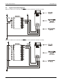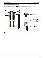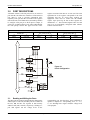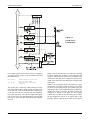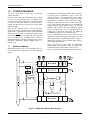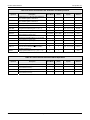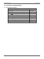
1
SX20AC/SX28AC Configurable Communications Controllers with EE/Flash Program Memory, In-System Programming Capability and On-Chip Debug 1.0 PRODUCT OVERVIEW 1.1. Introduction The Parallax SX family of configurable communications controllers is fabricated in an advanced CMOS process technology. The advanced process, combined with a RISC-like architecture, allows high-speed computation, flexible I/O control, and efficient data manipulation. Throughput is enhanced by operating the device at frequencies up to 75 MHz and by optimizing the instruction set to include mostly single-cycle instructions. The deterministic architecture of the SX provides reliable performance for time-critical applications. In addition, the SX architecture is flash-based and therefore reprogrammable. On-chip functions include a generalpurpose 8-bit timer with prescaler, an analog comparator, a brown-out detector, a watchdog timer, a power-save mode with multi-source wakeup capability, an internal R/C oscillator, user-selectable clock modes, and highcurrent outputs. These features enable the SX to be used as a general-purpose, high-speed microcontroller in a variety of applications. Figure 1-1: Block Diagram Parallax and the Parallax logo are trademarks of Parallax, Inc. SX is a trademark of Ubicom Inc, used with permission. © Parallax Inc. 2 I C is a trademark of Philips Corporation. All other trademarks are the property of their respective holders. Page 1 of 49 Rev 1.0 1/06 Parallax SX20AC/SX28AC www.parallax.com Table of Contents 1.0 Product Overview......................................................... 1 1.1. 1.2. 1.3. 1.4. Introduction ................................................................................1 Key Features..............................................................................3 Architecture................................................................................4 Programming Benefits in Assembly and High-Level Languages 4 1.4.1. Parallax SX/B Basic Compiler ...............................................................4 10.2. 10.3. Watchdog Timer ...................................................................... 26 The Prescaler .......................................................................... 26 11.0 Comparator .................................................................27 12.0 Reset ............................................................................28 1.5. 1.6. 1.7. 1.8. Programming and Debugging Support .......................................4 Applications................................................................................4 Support ......................................................................................4 Part Numbering..........................................................................5 13.0 Brown-Out Detector ...................................................29 14.0 Register States upon Different Reset Operations ...30 15.0 Instruction Set ............................................................31 2.0 Connection Diagrams .................................................. 6 2.1. 2.2. 2.3. Pin Assignments ........................................................................6 Pin Descriptions .........................................................................6 Typical Connection Diagrams ....................................................7 3.0 Port Descriptions ......................................................... 9 3.1. Reading and Writing the Ports ...................................................9 15.1. 15.2. 15.3. 15.4. 15.5. 15.6. 15.7. 15.8. 15.9. 15.10. Instruction Set Features........................................................... 31 Instruction Execution ............................................................... 31 Addressing Modes ................................................................... 31 RAM Addressing...................................................................... 32 The Bank Instruction................................................................ 32 Bit Manipulation ....................................................................... 32 Input/Output Operation ............................................................ 32 Increment/Decrement .............................................................. 32 Loop Counting and Data Pointing Testing................................ 32 Branch and Loop Call Instructions ........................................... 32 3.1.1. 3.2. 3.2.1. 3.2.2. 3.2.3. Read-Modify-Write Considerations......................................................11 Port Configuration ....................................................................11 MODE Register ...................................................................................11 Port Configuration Registers ...............................................................11 Port Configuration Upon Reset............................................................12 15.10.1. 15.10.2. 15.10.3. 15.10.4. Jump Operation .................................................................................. 33 Page Jump Operation......................................................................... 33 Call Operation..................................................................................... 33 Page Call Operation ........................................................................... 33 4.0 Special-Function Registers ....................................... 13 4.1. 4.2. 4.3. PC Register (02h) ....................................................................13 STATUS Register (03h) ...........................................................13 OPTION Register.....................................................................14 15.11. 15.12. 5.0 Device Configuration Registers................................ 15 5.1. 5.2. 5.3. FUSE Word (Read/Program at FFFh in Main Memory Map) ....15 FUSEX Word (Read/Program via Programming Command) ....16 DEVICE Word (Hard-Wired Read-Only)...................................16 15.13. 15.14. 15.15. 15.16. Comparison and Conditional Branch Instructions .................... 34 Logical Instruction.................................................................... 34 Shift and Rotate Instructions.................................................... 34 Complement and SWAP.......................................................... 34 6.0 Memory Organization ................................................ 17 16.0 Native SX Instruction Set Summary Tables .............35 6.1. Program Memory .....................................................................17 16.1. Equivalent Assembler Mnemonics ........................................... 39 Program Counter.................................................................................17 Subroutine Stack .................................................................................17 17.0 Electrical Characteristics...........................................40 17.1. 17.2. 17.3. 17.4. 17.5. Absolute Maximum Ratings ..................................................... 40 DC Characteristics................................................................... 41 AC Characteristics ................................................................... 42 Comparator DC and AC Specifications.................................... 42 Typical Performance Characteristics (25°C) ............................ 43 18.0 Package Dimensions..................................................46 18.1. 18.2. 18.3. SX20AC/SS ............................................................................. 46 SX28AC/SS ............................................................................. 47 SX28AC/DP............................................................................. 48 19.0 Manufacturing Information ........................................48 19.1. 19.2. 19.3. Reflow Peak Temperature ....................................................... 48 MSL3 Compliance ................................................................... 48 Green/RoHS Compliance ........................................................ 48 6.1.1. 6.1.2. 6.2. 6.2.1. Data Memory ...........................................................................17 File Select Register (04h)....................................................................17 7.0 Power Down Mode ..................................................... 19 7.1. 7.2. Multi-Input Wakeup ..................................................................19 Port B MIWU/Interrupt Configuration........................................20 8.0 Interrupt Support........................................................ 21 9.0 Oscillator Circuits ...................................................... 23 9.1. 9.2. 9.3. 9.4. XT, LP or HS modes ................................................................23 75 MHz Operation....................................................................25 External RC Mode....................................................................25 Internal RC Mode.....................................................................25 10.0 Real Time Clock (RTCC)/Watchdog Timer............... 26 10.1. RTCC.......................................................................................26 © Parallax Inc. 15.12.1. 15.12.2. Page 2 of 49 Return Instructions................................................................... 33 Subroutine Operation............................................................... 33 Push Operation................................................................................... 33 Pop Operation .................................................................................... 34 Rev 1.0 1/06 Parallax SX20AC/SX28AC 1.2. www.parallax.com Key Features Hardware Peripheral Features 75 MIPS Performance • SX20AC/SX28AC: DC - 75 MHz • SX20AC/SX28AC: as low as 13.3 ns instruction cycle, 39.9 ns internal interrupt response • 1 instruction per clock for most instructions (skips require 2 clocks, branches require 3 clocks, IREAD requires 4) EE/FLASH Program Memory and SRAM Data Memory • Access time of < 13.3 ns provides single cycle access • EE/Flash rated for > 10,000 rewrite cycles • 2048 Words EE/Flash program memory • 136x8 bits SRAM data memory • One 8-bit Real Time Clock/Counter (RTCC) with programmable 8-bit prescaler • Watchdog Timer (shares the RTCC prescaler) • Analog comparator • Brown-out detector • Multi-Input Wakeup logic on 8 pins • Internal RC oscillator with configurable rate from 31.25 kHz to 4 MHz • Power-On-Reset Packages • 20-pin SSOP, 28-pin DIP/SSOP Programming and Debugging Support CPU Features • Compact, RISC-like instruction set • All non-branch instructions are single cycle • Eight-level push/pop hardware stack for subroutine operation • Fast table lookup capability through run-time readable code (IREAD instruction) • Totally predictable program execution rate for precise real-time applications • On-chip in-system serial programming support via the oscillator pins • On-chip in-system debugging support logic • Real-time emulation, full program debug, and integrated development environment offered by the Parallax SX-Key® programming device • The language options available: Parallax Assembly; Parallax SX/B (BASIC); and CCS SX/C (C) Software Support Fast and Deterministic Interrupt • Jitter-free 3-cycle internal interrupt response • Hardware context save/restore of key resources such as PC, W, STATUS, and FSR within the 3-cycle interrupt response time • External wakeup/interrupt capability on Port B (8 pins) • Native assembly instruction set • Expanded assembly instruction set available in the SASM assembler of the Parallax SX-Key IDE • Parallax SX/B compiler (BASIC) • Several “C” compliers available from third-party vendors Flexible I/O • • • • • • • All port pins individually programmable as I/O Inputs are TTL or CMOS level selectable All pins have selectable internal pull-ups Selectable Schmitt Trigger inputs on Ports B and C All output pins capable of sourcing/sinking 30 mA Port A outputs have symmetrical drive Analog comparator support on Port B (RB0 OUT, RB1 IN-, RB2 IN+) • Selectable I/O operation synchronous to the oscillator clock © Parallax Inc. Page 3 of 49 Rev 1.0 1/06 Parallax SX20AC/SX28AC 1.3. www.parallax.com Architecture The SX devices use a modified Harvard architecture. This architecture uses two separate memories with separate address buses, one for the program and one for data, while allowing transfer of data from program memory to SRAM. This ability allows accessing data tables from program memory. The advantage of this architecture is that instruction fetch and memory transfers can be overlapped with a multi-stage pipeline, which means the next instruction can be fetched from program memory while the current instruction is being executed using data from the data memory. This RISC-like architecture and memory design is based on technology that makes it very fast, deterministic, jitter free, and totally reprogrammable. The SX family implements a four-stage pipeline (fetch, decode, execute, and write back), which results in execution of one instruction per clock cycle. For example, at the maximum operating frequency of 75 MHz, instructions are executed at the rate of one per 13.3 ns clock cycle. 1.4. Programming Benefits in Assembly and High-Level Languages The SX’s high speed enables a “software system on a chip” approach. Programming in assembly language provides a particularly high-level of access to the interrupt service routine, the stack and registers to take the highest advantage of the SX’s deterministic timing. The primary technical resources for programming the SX in assembly language include the following: • The SX20AC/SX28AC datasheet • SX-Key Development System User’s Manual by Parallax, Inc. • Programming the SX Microcontroller – A Complete Guide by Guenther Daubach Customers with a high-level programming language background may prefer the use of a C or BASIC compiler. 1.4.1. Parallax SX/B Basic Compiler Parallax's SX/B is a free BASIC language compiler for the SX microcontroller (SX20, SX28, and SX48). The compiler speeds the programming of the SX microcontrollers by providing a simple, yet robust highlevel language familiar to Parallax customers. SX/B includes the following features and commands: • ASM directive to support in-line assembly language • Program structure commands including BRANCH, DO..LOOP, GOTO, GOSUB, IF..THEN..ELSE • Numeric formatters • WORD variable support • Frequency generation with FREQOUT © Parallax Inc. • Synchronous serial communication for I2C, 1-Wire, SPI • Asynchronous serial communication with SERIN and SEROUT • Table data storage and retrieval with LOOKUP, LOOKDOWN • I/O pin control with HIGH, LOW, TOGGLE, REVERSE • Timing and delay with PAUSE, SLEEP • PULSIN and PULSOUT • Resistor/capacitor A/D with RCTIME • RANDOM for pseudo-random number generation • Non-volatile EEPROM memory access with DATA, READ • Low-current SLEEP command The complete SX/B command reference and examples are installed with the SX-Key IDE. 1.5. Programming and Debugging Support The SX devices are supported by Parallax’s programming and debugging tools. The Parallax SX-Blitz is a programming tool. The SX-Key supports programming and source-level debugging. On-chip in-system debug capabilities allow the Parallax tool to be an all-in-one integrated development environment with editor, macro assembler, debugger, and programmer. Unobtrusive insystem programming is provided through the OSC pins. Visit www.parallax.com for the SX-Key development tools, the IDE and support forum information. The in-system programming specification is available to other 3rd party tool vendors upon request. 1.6. Applications The SX may be used as a solution for process controllers, electronic appliances/tools, security/monitoring systems, sound and signal generation, GPS interface, robotic control, motor control, sensor interfacing and personal communication devices. Applications such as interactive toys, magnetic-stripe readers, infrared decoders, and other timing-sensitive projects are also common with the SX. Examples of customer applications may be seen on the Parallax web site. 1.7. Support Parallax and our distributors provide all support for the SX microcontroller. Support is available free of charge via phone (888) 512-1024 in the U.S. Also be sure to participate in the SX discussion forum at http://forums.parallax.com/forums/. The on-line SX support community is actively involved in customer support 24 hours a day. Page 4 of 49 Rev 1.0 1/06 Parallax SX20AC/SX28AC 1.8. www.parallax.com Part Numbering Table 1-1: Part Numbering Device Part# SX20AC/SS Pins I/O EE/Flash (Words) RAM (Bytes) Operating Temp 20 12 2K 137 -40 °C to +85 °C SX20AC/SS-G 20 12 2K 137 0 °C to +70 °C SX28AC/DP 28 20 2K 136 -40 °C to +85 °C SX28AC/DP-G 28 20 2K 136 0 °C to +70 °C SX28AC/SS 28 20 2K 136 -40 °C to +85 °C SX28AC/SS-G 28 20 2K 136 0 °C to +70 °C Figure 1-2 Part Number Reference Guide © Parallax Inc. Page 5 of 49 Rev 1.0 1/06 Parallax SX20AC/SX28AC www.parallax.com 2.0 CONNECTION DIAGRAMS 2.1. Pin Assignments Figure 2-1: Pin Assignments 2.2. Pin Descriptions Table 2-1: Pin Descriptions Name Description Pin Type Input Levels RA0 I/O TTL/CMOS Bidirectional I/O Pin; symmetrical source / sink capability RA1 I/O TTL/CMOS Bidirectional I/O Pin; symmetrical source / sink capability RA2 I/O TTL/CMOS Bidirectional I/O Pin; symmetrical source / sink capability RA3 I/O TTL/CMOS Bidirectional I/O Pin; symmetrical source / sink capability RB0 I/O TTL/CMOS/ST Bidirectional I/O Pin; comparator output; MIWU/Interrupt input RB1 I/O TTL/CMOS/ST Bidirectional I/O Pin; comparator negative input; MIWU/Interrupt input RB2 I/O TTL/CMOS/ST Bidirectional I/O Pin; comparator positive input; MIWU/Interrupt input RB3 I/O TTL/CMOS/ST Bidirectional I/O Pin; MIWU/Interrupt input RB4 I/O TTL/CMOS/ST Bidirectional I/O Pin; MIWU/Interrupt input RB5 I/O TTL/CMOS/ST Bidirectional I/O Pin; MIWU/Interrupt input RB6 I/O TTL/CMOS/ST Bidirectional I/O Pin; MIWU/Interrupt input RB7 I/O TTL/CMOS/ST Bidirectional I/O Pin; MIWU/Interrupt input RC0 I/O TTL/CMOS/ST Bidirectional I/O Pin RC1 I/O TTL/CMOS/ST Bidirectional I/O Pin RC2 I/O TTL/CMOS/ST Bidirectional I/O Pin RC3 I/O TTL/CMOS/ST Bidirectional I/O Pin RC4 I/O TTL/CMOS/ST Bidirectional I/O Pin RC5 I/O TTL/CMOS/ST Bidirectional I/O Pin RC6 I/O TTL/CMOS/ST Bidirectional I/O Pin RC7 I/O TTL/CMOS/ST Bidirectional I/O Pin RTCC I ST MCLR I ST OSC1/In/Vpp I ST Input to Real-time Clock/counter Master Clear reset input – active low. When not controlled externally, this pin must be pulled high with a 10 kΩ resistor. Crystal oscillator input; external clock source input OSC2/Out O CMOS Crystal oscillator output; in R/C mode, internally pulled to Vdd through weak pull-up Vdd P - Positive supply pin P Ground pin Vss Note: I = input, O = output, I/O = Input/Output, P = Power, TTL = TTL input, CMOS = CMOS input, ST = Schmitt Trigger input, MIWU = Multi-Input Wakeup input. © Parallax Inc. Page 6 of 49 Rev 1.0 1/06 Parallax SX20AC/SX28AC 2.3. www.parallax.com Typical Connection Diagrams Note: The 10 kΩ resistor connected to the MCLR pin is not needed when controlled externally. Note: The 10 kΩ resistor connected to the MCLR pin is not needed when controlled externally. © Parallax Inc. Page 7 of 49 Rev 1.0 1/06 Parallax SX20AC/SX28AC www.parallax.com Typical Connection Diagrams (continued) Note: The 10 kΩ resistor connected to the MCLR pin is not needed when controlled externally. © Parallax Inc. Page 8 of 49 Rev 1.0 1/06 Parallax SX20AC/SX28AC 3.0 www.parallax.com PORT DESCRIPTIONS All models contain a 4-bit I/O port (Port A), an 8-bit I/O port (Port B). The SX28 also contains a second 8-bit I/O port (Port C). Port A provides symmetrical drive capability. Each port has three associated 8-bit registers (Direction, Data, TTL/CMOS Select, and Pull-Up Enable) to configure each port pin as Hi-Z input or output, to select TTL or CMOS voltage levels, and to enable/disable the weak pull-up resistor. The upper four bits of the registers associated with Port A are not used. The least significant bit of the registers corresponds to the least significant port pin. To access these registers, an appropriate value must be written into the MODE register. Upon power-up, all bits in these registers are initialized to “1”. The associated registers allow for each port bit to be individually configured under software controls as shown below. Table 3-1: Port Configuration Data Direction Registers: RA, RB, RC 0 1 Output Hi-Z Input TTL/CMOS Selected Registers: LVL_A, LVL_B, LVL_C 0 1 CMOS TTL Pullup Enable Registers: PLP_A, PLP_B, PLP_C 0 1 Enable Disable Figure 3-1 Port A Configuration 3.1. Reading and Writing the Ports The three ports are memory-mapped into the data memory address space. To the CPU, the three ports are available as the RA, RB, and RC file registers at data memory addresses 05h, 06h, and 07h, respectively. Writing to a port data register sets the voltage levels of the © Parallax Inc. corresponding port pins that have been configured to operate as outputs to a corresponding level, 1 = 5 V, 0 = 0 V. Reading from a register reads the voltage levels of all port pins. Page 9 of 49 Rev 1.0 1/06 Parallax SX20AC/SX28AC www.parallax.com Figure 3-2 Port B, Port C Configuration For example, suppose all four Port A pins are configured as outputs and you wish to set RA0 and RA1 high, and RA2 and RA3 low: mov W,#$03 mov $05,W ;load W with the value 03h ;(bits 0 and 1 high) ;write 03h to Port A data ;register The second “mov” instruction in this example writes the Port A data register (RA), which controls the output levels of the four Port A pins, RA0 through RA3. Because Port A has only four I/O pins, only the four least significant bits of this register are used. The four high-order register bits are “don’t care” bits. Port B and Port C are both eight bits wide, so the full widths of the RB and RC registers are used. © Parallax Inc. When a write is performed to a bit position for a port that has been configured as an input, a write to the port data register is still performed, but it has no immediate effect on the pin. If later that pin is configured to operate as an output, it will reflect the value that has been written to the data register. When a read is performed from a bit position for a port, the operation is actually reading the voltage level on the pin itself, not necessarily the bit value stored in the port data register. This is true whether the pin is configured to operate as an input or an output. Therefore, with the pin configured to operate as an input, the data register contents have no effect on the value that you read. With the pin configured to operate as an output, what is read generally matches what has been written to the register. Page 10 of 49 Rev 1.0 1/06 Parallax SX20AC/SX28AC www.parallax.com 3.1.1. Read-Modify-Write Considerations Caution must be exercised when performing two successive read-modify-write instructions (SETB or CLRB operations) on an I/O port pin. Input data used for an instruction must be valid during the time the instruction is executed, and the output result from an instruction is valid only after that instruction completes its operation. Unexpected results from successive readmodify-write operations on I/O pins can occur when the device is running at high speeds. Although the device has an internal write-back section to prevent such conditions, it is still recommended that the user program include a NOP instruction as a buffer between successive readmodify-write instructions performed on I/O pins of the same port. Also note that reading an I/O port is actually reading the pins, not the output data latches. That is, if the pin output driver is enabled and driven high while the pin is held low externally, the port pin will read low. 3.2. “mov !rx,W” instruction as indicated in Table 2-1. MODE register values not listed in the table are reserved for future expansion and should not be used. Therefore, the MODE register should always contain a value from 08h to 0Fh. Upon reset, the MODE register is initialized to 0Fh, which enables access to the port direction registers. After a value is written to the MODE register, that setting remains in effect until it is changed by writing to the MODE register again. For example, you can write the value 0Eh to the MODE register just once, and then write to each of the three pullup configuration registers using the three “mov !rx,W” instructions. Table 3-2: MODE Register and Port Control Register Access MODE Reg. Mov !RA,W Mov !RB, W Mov !Rc, W 08h not used CMP_B not used 09h not used WKPND_B not used 0Ah not used WKED_b not used 0Bh not used WKEN_B not used 0Ch not used ST_B ST_C Port Configuration Each port pin offers the following configuration options: • • • • data direction input voltage levels (TTL or CMOS) pullup type (pullup resistor enable or disable) Schmitt trigger input (for Port B and Port C only) Port B offers the additional option to use the port pins for the Multi-Input Wakeup/Interrupt function and/or the analog comparator function. Port configuration is performed by writing to a set of control registers associated with the port. A specialpurpose instruction is used to write these control registers: • mov !RA,W (move W to Port A control register) • mov !RB,W (move W to Port B control register) • mov !RC,W (move W to Port C control register) Each one of these instructions writes a port control register for Port A, Port B, or Port C. There are multiple control registers for each port. To specify which one you want to access, you use another register called the MODE register. 3.2.1. MODE Register The MODE register controls access to the port configuration registers. Because the MODE register is not memory-mapped, it is accessed by the following special purpose instructions: • mov M, #lit (move literal to MODE register) • mov M,W (move W to MODE register) • mov W,M (move MODE register to W) LVL_A LVL_B LVL_C 0Eh PLP_A PLP_B PLP_C 0Fh RA Direction RB Direction RC Direction The following code example shows how to program the pullup control registers. mov M,#$0E ;MODE=0Eh to access port pullup ;registers mov W,#$03 mov !RA,W ;W = 0000 0011 ;disable pullups for RA0 and RA1 mov W,#$FF mov !RB,W ;W = 1111 1111 ;disable all pullups for RB0-RB7 mov W,#$00 mov !RC,W ;W = 0000 0000 ;enable all pullups for RC0-RC7 First the MODE register is loaded with 0Eh to select access to the pullup control registers (PLP_A, PLP_B, and PLP_C). Then the “mov !rx,W” instructions are used to specify which port pins are to be connected to the internal pullup resistors. Setting a bit to 1 disconnects the corresponding pullup resistor, and clearing a bit to 0 connects the corresponding pullup resistor. 3.2.2. Port Configuration Registers The port configuration registers that you control with the “mov !rx,W” instruction operate as described below. RA, RB, and RC Data Direction Registers (MODE=0Fh) The value contained in the MODE register determines which port control register is accessed by the © Parallax Inc. 0Dh Each register bit sets the data direction for one port pin. Set the bit to 1 to make the pin operate as a highimpedance input. Clear the bit to 0 to make the pin operate as an output. Page 11 of 49 Rev 1.0 1/06 Parallax SX20AC/SX28AC www.parallax.com PLP_A, PLP_B, and PLP_C: Pullup Enable Registers (MODE=0Eh) WKPND_B: Wakeup Pending Bit Register (MODE=09h) Each register bit determines whether an internal pullup resistor is connected to the pin. Set the bit to 1 to disconnect the pullup resistor or clear the bit to 0 to connect the pullup resistor. When you access the WKPND_B register using “mov !rx,W”, the CPU does an exchange between the contents of W and WKPND_B. This feature lets you read the WKPND_B register contents while clearing the Wakeup Pending bits simultaneously. Each bit indicates the status of the corresponding MIWU pin. A bit set to 1 indicates that a valid edge has occurred on the corresponding MIWU pin, triggering a wakeup or interrupt. A bit set to 0 indicates that no valid edge has occurred on the MIWU pin. LVL_A, LVL_B, and LVL_C: Input Level Registers (MODE=0Dh) Each register bit determines the voltage levels sensed on the input port, either TTL or CMOS, when the Schmitt trigger option is disabled. Program each bit according to the type of device that is driving the port input pin. Set the bit to 1 for TTL or clear the bit to 0 for CMOS. ST_B and ST_C: Schmitt Trigger Enable Registers (MODE=0Ch) Each register bit determines whether the port input pin operates with a Schmitt trigger. Set the bit to 1 to disable Schmitt trigger operation and sense either TTL or CMOS voltage levels; or clear the bit to 0 to enable Schmitt trigger operation. WKEN_B: Wakeup Enable Register (MODE=0Bh) Each register bit enables or disables the Multi-Input Wakeup/Interrupt (MIWU) function for the corresponding Port B input pin. Clear the bit to 0 to enable MIWU operation or set the bit to 1 to disable MIWU operation. For more information on using the Multi-Input Wakeup/Interrupt function, see Section 7.1. WKED_B: Wakeup Edge Register (MODE=0Ah) Each register bit selects the edge sensitivity of the Port B input pin for MIWU operation. Clear the bit to 0 to sense rising (low-to-high) edges. Set the bit to 1 to sense falling (high-to-low) edges. © Parallax Inc. CMP_B: Comparator Register (MODE=08h) When you access the CMP_B register using MOV !RB,W, the CPU does an exchange between the contents of W and CMP_B. This feature lets you read the CMP_B register contents. Clear bit 7 to enable operation of the comparator. Clear bit 6 to place the comparator result on the RB0 pin. Bit 0 is a result bit that is set to 1 when the voltage on RB2 is greater than RB1, or cleared to 0 otherwise. (For more information using the comparator, see Section 11.0.) 3.2.3. Port Configuration Upon Reset Upon reset, all the port control registers are initialized to FFh. Thus, each pin is configured to operate as a high impedance input that senses TTL voltage levels, with no internal pullup resistor connected. The MODE register is initialized to 0Fh, which allows immediate access to the data direction registers using the “mov !rx,W” instruction. Page 12 of 49 Rev 1.0 1/06 Parallax SX20AC/SX28AC 4.0 www.parallax.com SPECIAL-FUNCTION REGISTERS The CPU uses a set of special-function registers to control the operation of the device. The CPU registers include an 8-bit working register (W), which serves as a pseudo accumulator. It holds the second operand of an instruction, receives the literal in immediate type instructions, and also can be program selected as the destination register. A set of 31 file registers serves as the primary accumulator. One of these registers holds the first operand of an instruction and another can be program-selected as the destination register. The first eight file registers include the Real-Time Clock/Counter register (RTCC), the lower eight bits of the 11-bit Program Counter (PC), the 8-bit STATUS register, three port control registers for Port A, Port B, Port C, the 8-bit File Select Register (FSR), and INDF used for indirect addressing. The five low-order bits of the FSR register select one of the 31 file registers in the indirect addressing mode. Calling for the file register located at address 00h (INDF) in any of the file-oriented instructions selects indirect addressing, which uses the FSR register. It should be noted that the file register at address 00h is not a physically implemented register. The CPU also contains an 8 level, 11-bit hardware push/pop stack for subroutine linkage. Table 4-1: Special-Function Register Address 00h Name INDF Function Used for indirect addressing 01h RTCC Real Time Clock/Counter 02h PC Program Counter (low byte) 03h STATUS Holds status bits of ALU 04h FSR File Select Register 05h RA Port RA control register 06h RB Port RB control register 07h RC* Port RC control register *In the SX20 package, Port C is not used, and address 07h is available as a general-purpose RAM location. 4.1. PC Register (02h) The PC register holds the lower eight bits of the program counter. It is accessible at run time to perform branch operations. 4.2. STATUS Register (03h) The STATUS register holds the arithmetic status of the ALU, the page select bits, and the reset state. The STATUS register is accessible during run time, except that bits PD and TO are read-only. It is recommended that only SETB and CLRB instructions be used on this © Parallax Inc. register. Care should be exercised when writing to the STATUS register as the ALU status bits are updated upon completion of the write operation, possibly leaving the STATUS register with a result that is different than intended. PA2 Bit 7 PA1 PA0 TO PD Z DC C Bit 0 Bit 7-5: Page select bits PA2:PA0 000 = Page 0 (000h - 01FFh) 001 = Page 1 (200h - 03FFh) 010 = Page 2 (400h - 05FFh) 011 = Page 3 (600h - 07FFh) Bit 4: Time Out bit, TO 1 = Set to 1 after power up and upon execution of CLRWDT or SLEEP instructions 0 = A watchdog time-out occurred Bit 3: Power Down bit, PD 1= Set to a 1 after power up and upon execution of the CLRWDT instruction 0 = Cleared to a ‘0’ upon execution of SLEEP instruction Bit 2: Zero bit, Z 1 = Result of math operation is zero 0 = Result of math operation is non-zero Bit 1: Digit Carry bit, DC After Addition: 1 = A carry from bit 3 occurred 0 = No carry from bit 3 occurred After Subtraction: 1 = No borrow from bit 3 occurred 0 = A borrow from bit 3 occurred Bit 0: Carry bit, C After Addition: 1 = A carry from bit 7 of the result occurred 0 = No carry from bit 7 of the result occurred After Subtraction: 1 = No borrow from bit 7 of the result occurred 0 = A borrow from bit 7 of the result occurred Rotate (RR or RL) Instructions: The carry bit is loaded with the low or high order bit, respectively. When CF bit is cleared, Carry bit works as input For ADD and SUB instructions. Page 13 of 49 Rev 1.0 1/06 Parallax SX20AC/SX28AC 4.3. RTW www.parallax.com OPTION Register RTW_IE Bit 7 RTS RTE_ES PSA PS2 PS1 PS0 Bit 0 When the OPTIONX bit in the FUSE word is cleared, bits 7 and 6 of the OPTION register function as described below. When the OPTIONX bit is set, bits 7 and 6 of the OPTION register read as ‘1’s. RTW RTCC/W register selection: 0 = Register 01h addresses W 1 = Register 01h addresses RTCC RTE_IE RTCC edge interrupt enable: 0 = RTCC roll-over interrupt is enabled 1 = RTCC roll-over interrupt is disabled RTS RTCC increment select: 0= RTCC increments on internal instruction cycle 1 = RTCC increments upon transition on RTCC pin RTE_ES RTCC edge select: 0 = RTCC increments on low-to-high transitions 1 = RTCC increments on high-to-low transitions PSA Prescaler Assignment: 0 = Prescaler is assigned to RTCC, with divide rate determined by PS0-PS2 bits 1 = Prescaler is assigned to WDT, and divide rate on RTCC is 1:1 PS2-PS0: Prescaler divider (see table below) Table 4-2: Prescaler Divider Ratios PS2, PS1, PS0 RTCC Divide Rate Watchdog Timer Divide Rate 000 1:2 1:1 001 1:4 1:2 010 1:8 1:4 011 1:16 1:8 100 1:32 1:16 101 1:64 1:32 110 1:128 1:64 07h111 1:256 1:128 Upon reset, all bits in the OPTION register are set to 1. © Parallax Inc. Page 14 of 49 Rev 1.0 1/06 Parallax SX20AC/SX28AC 5.0 www.parallax.com DEVICE CONFIGURATION REGISTERS The SX device has three registers (FUSE, FUSEX, DEVICE) that control functions such as operating the device in Turbo mode, extended (8-level deep) stack operation, and speed selection for the internal RC oscillator. These registers are not programmable “on the 5.1. TURBO fly” during normal device operation. Instead, the FUSE and FUSEX registers can only be accessed when the SX device is being programmed. The DEVICE register is a read-only, hard-wired register, programmed during the manufacturing process. FUSE Word (Read/Program at FFFh in Main Memory Map) SYNC Reserved Reserved IRC DIV1/ DIV0/ IFBD FOSC2 Reserved CP WDTE Bit 11 FOSC1 FOSC0 Bit 0 TURBO Turbo mode enable: 0 = turbo (instruction clock = osc/1) 1 = instr clock = osc/4 SYNC Synchronous input enable (for turbo mode): This bit synchronizes the signal presented at the input pin to the internal clock through two internal flip-flops. 0 = enabled 1 = disabled IRC Internal RC oscillator enable: 0 = enabled - OSC1 pulled low by weak pullup, OSC2 pulled high by weak pullup 1 = disabled - OSC1 and OSC2 behave according to FOSC2: FOSC0 Internal RC oscillator divider: 00b = 4 MHz 01b = 1 MHz 10 = 128 KHz 11b = 32 KHz DIV1: DIV0 IFBD Internal crystal/resonator oscillator feedback resistor (1 MΩ: 0 = disabled Internal feedback resistor disable (external feedback required) 1= enabled Internal feedback resistor enabled (valid when IRC = 1) CP Code protect enable: 0 = enabled (FUSE, code, and ID memories read back as garbled data) 1 = disabled (FUSE, code, and ID memories can be read normally) WDTE Watchdog timer enable: 0 = disabled 1 = enabled FOSC2: FOSC0 External oscillator configuration (valid when IRC = 1): 000b = LP1 - low power crystal (32KHz) 001b = LP2 - low power crystal/resonator (32 KHz to 1 MHz) 010b = XT1 - normal crystal/resonator (32 kHz to 10 MHz) 011b = XT2 - normal crystal/resonator (1MHz to 24 MHz) 100b = HS1 - high speed crystal/resonator/external crystal oscillator (1MHz to 50 MHz) 101b = HS2 - high speed crystal/resonator/external crystal oscillator (1 MHz to 50 MHz) 110b = HS3 - high speed crystal/resonator/external crystal oscillator (1 MHz to 75 MHz) 111b = RC network - OSC2 is pulled high with a weak pullup (no CLKOUT output) Note: The frequencies are target values. © Parallax Inc. Page 15 of 49 Rev 1.0 1/06 Parallax SX20AC/SX28AC 5.2. www.parallax.com FUSEX Word (Read/Program via Programming Command) IRCTRIM2 PINS IRCTRIM1 IRCTRIM0 OPTIONX / CF STACKX BOR1 BOR0 BORTR1 BORTR0 BP1 Bit 11 BP0 Bit 0 IRCTRIM2: IRCTRIM0 Internal RC oscillator trim bits. This 3-bit field adjusts the operation of the internal RC oscillator to make it operate within the target frequency range 4 MHz plus or minus 8%. Parts are shipped from the factory untrimmed. The device relies on the programming to0l to provide the trimming function. 000b = minimum frequency 111b = maximum frequency each step about 3% Selects the number of pins. 0 = 18/20 pins 1 = 28 pins PINS OPTIONX / STACKX OPTION Register Extension and Stack Extension. Set to 1 to disable the programmability of bit 6 and bit 7 in the OPTION register, the RTW and RTE_IE bits (in other words, to force these two bits to 1) and to limit the program stack size to two locations. Clear to 0 to enable programming of the RTW and RTE_IE bits in the OPTION register, and to extend the stack size to eight locations. CF Active low - makes carry bit input to ADD and SUB instructions. Brown-Out Reset: These bits enable or disable the brown-out reset function and set the brown-out threshold voltage as follows: 00b = 4.2 V 01b = 2.6 V 10b = 2.2 V 11b = Brown-Out disabled Brown-Out trim bits (parts are shipped out of factory untrimmed). 01b = minimum threshold voltage 00b = LOW 11b = HIGH 10b = maximum threshold voltage 00b = 1 page, 1 bank 01b = 2 pages, 1 bank 10b = 4 pages, 4 banks 11b = 4 pages, 8 banks (default configuration) BOR1: BOR0 BORTR1: BORTR0 BP1:BPO 5.3. DEVICE Word (Hard-Wired Read-Only) 1 1 1 1 1 1 0 Bit 11 © Parallax Inc. 0 1 1 1 0 Bit 0 Page 16 of 49 Rev 1.0 1/06 Parallax SX20AC/SX28AC 6.0 MEMORY ORGANIZATION 6.1. Program Memory www.parallax.com 6.2. The program memory is organized as 2K, 12-bit wide words. The program memory words are addressed sequentially by a binary program counter. The program counter starts at zero. If there is no branch operation, it will increment to the maximum value possible for the device and roll over and begin again. Internally, the program memory has a semi-transparent page structure. A page is composed of 512 contiguous program memory words. The lower nine bits of the program counter are zeros at the first address of a page and ones at the last address of a page. This page structure has no effect on the program counter. The program counter will freely increment through the page boundaries. 6.1.1. Program Counter The program counter contains the 11-bit address of the instruction to be executed. The lower eight bits of the program counter are contained in the PC register (02h) while the upper bits come from the upper three bits of the STATUS register (PA0, PA1, PA2). This is necessary to cause jumps and subroutine calls across program memory page boundaries. Prior to the execution of a branch operation, the user program must initialize the upper bits of the STATUS register to cause subsequent branch instructions to vector to the desired page. An alternative method is to use the PAGE instruction, which automatically causes subsequent branch instructions to branch vector to the desired page, based on the value specified in the operand field. Upon reset, the program counter is initialized with 07FFh. 6.1.2. Subroutine Stack The subroutine stack consists of eight 11-bit save registers. A physical transfer of register contents from the program counter to the stack or vice versa, and within the stack, occurs on all operations affecting the stack, primarily calls and returns. The stack is physically and logically separate from data RAM. The program cannot read or write the stack. © Parallax Inc. Data Memory The data memory consists of 136 bytes of RAM, organized as eight banks of 16 registers plus eight registers which are not banked. Both banked and nonbanked memory locations can be addressed directly or indirectly using the FSR (File Select Register). The special-function registers are mapped into the data memory. 6.2.1. File Select Register (04h) Instructions that specify a register as the operand can only express five bits of register address. This means that only registers 00h to 1Fh can be accessed. The File Select Register (FSR) provides the ability to access registers beyond 1Fh. Figure 6-1 shows how FSR can be used to address RAM locations. The three high-order bits of FSR select one of eight SRAM banks to be accessed. The five low-order bits select one of 32 SRAM locations within the selected bank. FSR.4 essentially enables or disables banked RAM. For the lower 16 addresses, Bank 0 is always accessed, irrespective of the three high-order bits. Thus, RAM register addresses 00h through 0Fh are “global” in that they can always be accessed, regardless of the contents of the FSR. The entire data memory (including the dedicated-function registers) consists of the lower 16 bytes of Bank 0 and the upper 16 bytes of Bank 0 through Bank 7, for a total of (1+8)*16 = 144 bytes. Eight of these bytes are for the function registers, leaving 136 general-purpose memory locations. In the 18-pin SX packages, register RC is not used, which makes address 07h available as an additional general-purpose memory location. Below is an example of how to write to register 10h in Bank 4: mov FSR,#$90 mov $10,#$64 Page 17 of 49 ;Select Bank 4 by ;setting FSR<7:5> ;load register 10h with ;the literal 64h Rev 1.0 1/06 Parallax SX20AC/SX28AC www.parallax.com Figure 6-1: Data Memory Organization © Parallax Inc. Page 18 of 49 Rev 1.0 1/06 Parallax SX20AC/SX28AC 7.0 www.parallax.com POWER DOWN MODE The power down mode is entered by executing the SLEEP instruction. In power down mode, only the Watchdog Timer (WDT) is active. If the Watchdog Timer is enabled, upon execution of the SLEEP instruction, the Watchdog Timer is cleared, the TO (time out) bit is set in the STATUS register, and the PD (power down) bit is cleared in the STATUS register. There are three different ways to exit from the power down mode: a timer overflow signal from the Watchdog Timer (WDT), a valid transition on any of the Multi-Input Wakeup pins (Port B pins), or through an external reset input on the MCLR pin. To achieve the lowest possible power consumption, the Watchdog Timer should be disabled and the device should exit the power down mode through the Multi-Input Wakeup (MIWU) pins or an external reset. 7.1. Multi-Input Wakeup Multi-Input Wakeup is one way of causing the device to exit the power down mode. Port B is used to support this feature. The WKEN_B register (Wakeup Enable Regis ter) allows any Port B pin or combination of pins to cause the wakeup. Clearing a bit in the WKEN_B register enables the wakeup on the corresponding Port B pin. If multiinput wakeup is selected to cause a wakeup, the trigger condition on the selected pin can be either rising edge (low to high) or falling edge (high to low). The WKED_B register (Wakeup Edge Select) selects the desired transition edge. Setting a bit in the WKED_B register selects the falling edge on the corresponding Port B. Clearing the bit selects the rising edge. The WKEN_B and WKED_B registers are set to FFh upon reset. Once a valid transition occurs on the selected pin, the WKPND_B register (Wakeup Pending Register) latches the transition in the corresponding bit position. A logic ‘1’ indicates the occurrence of the selected trigger edge on the corresponding Port B pin. Upon exiting the power down mode, the Multi-Input Wakeup logic causes program counter to branch to the maximum program memory address (same as reset). Figure 7-1 shows the Multi-Input Wakeup block diagram. Figure 7-1: Multi-Input Wakeup Block Diagram © Parallax Inc. Page 19 of 49 Rev 1.0 1/06 Parallax SX20AC/SX28AC 7.2. www.parallax.com Port B MIWU/Interrupt Configuration The WKPND_B register comes up with an unknown value upon reset. The user program must clear the register prior to enabling the wake-up condition or interrupts. The proper initialization sequence is: 1. Select the desired edge (through WKED_B register). 2. Clear the WKPND_B register. 3. Enable the Wakeup condition (through WKEN_B register). Below is an example of how to read the WKPND_B register to determine which Port B pin caused the wakeup or interrupt, and to clear the WKPND_B register: mov clr mov M,#$09 W RB,W ;W contains WKPND_B ;contents of W exchanged ;with contents of WKPND_B mov mov mov mov mov mov mov mov mov mov mov The final “mov” instruction in this example performs an exchange of data between the working register (W) and the WKPND_B register. This exchange occurs only with Port B accesses. Otherwise, the “mov” instruction does not perform an exchange, but only moves data from the source to the destination. © Parallax Inc. Here is an example of a program segment that configures the RB0, RB1, and RB2 pins to operate as Multi Input Wakeup/Interrupt pins, sensitive to falling edges: M,#$0F ;prepare to write port data ;direction registers W,#$07 ;load W with the value 07h RB,W ;configure RB0-RB2 to be inputs M,#$0A ;prepare to write WKED_B ;(edge) register ;W contains the value 07h !RB,W ;configure RB0-RB2 to sense ;falling edges M,#$09 ;prepare to access WKPND_B ;(pending) register W,#$00 ;clear W !RB,W ;clear all wakeup pending bits M,#$0B ;prepare to write WKEN_B (enable) ;register W,#$F8h ;load W with the value F8h !RB,W ;enable RB0-RB2 to operate as ;wakeup inputs To prevent false interrupts, the enabling step (clearing bits in WKEN_B) should be done as the last step in a sequence of Port B configuration steps. After this program segment is executed, the device can receive interrupts on the RB0, RB1, and RB2 pins. If the device is put into the power down mode (by executing the SLEEP instruction), the device can then receive wakeup signals on those same pins. Page 20 of 49 Rev 1.0 1/06 Parallax SX20AC/SX28AC 8.0 www.parallax.com INTERRUPT SUPPORT The device supports both internal and external maskable interrupts. The internal interrupt is generated as a result of the RTCC rolling over from 0FFh to 00h. This interrupt source has an associated enable bit located in the OPTION register. There is no pending bit associated with this interrupt. Port B provides the source for eight external software selectable, edge sensitive interrupts. These interrupt sources share logic with the Multi-Input Wakeup circuitry. The WKEN_B register allows interrupt from Port B to be individually enabled or disabled. Clearing a bit in the WKEN_B register enables the interrupt on the corresponding Port B pin. The WKED_B selects the transition edge to be either positive or negative. The WKEN_B and WKED_B registers are set to FFh upon reset. Setting a bit in the WKED_B register selects the falling edge while clearing the bit selects the rising edge on the corresponding Port B pin. The WKPND_B register serves as the external interrupt pending register. The WKPND_B register comes up a with random value upon reset. The user program must clear the WKPND_B register prior to enabling the interrupt. The proper sequence is described in Section 7.2 Figure 8-1 shows the structure of the interrupt logic. Figure 8-1: Interrupt Structure © Parallax Inc. Page 21 of 49 Rev 1.0 1/06 Parallax SX20AC/SX28AC www.parallax.com All interrupts are global in nature; that is, no interrupt has priority over another. Interrupts are handled sequentially. Figure 8-2 shows the interrupt processing sequence. Once an interrupt is acknowledged, all subsequent global interrupts are disabled until return from servicing the current interrupt. The PC is pushed onto the single level interrupt stack, and the contents of the FSR, STATUS, and W registers are saved in their corresponding shadow registers. The status bits PA0, PA1, and PA2 bits are cleared after the STATUS register has been saved in its shadow register. The interrupt logic has its own singlelevel stack and is not part of the CALL subroutine stack. The vector for the interrupt service routine is address 0. Once in the interrupt service routine, the user program must check all external interrupt pending bits (contained in the WKPND_B register) to determine the source of the interrupt. The interrupt service routine should clear the corresponding interrupt pending bit. If both internal and external interrupts are enabled, the user program may also need to read the contents of RTCC to determine any recent RTCC rollover. This is needed since there is no interrupt pending bit associated with the RTCC rollover. Normally it is a requirement for the user program to process every interrupt without missing any. To ensure this, the longest path through the interrupt routine must take less time than the shortest possible delay between interrupts. If an external interrupt occurs during the interrupt routine, the pending register will be updated but the trigger will be ignored unless interrupts are disabled at the beginning of the interrupt routine and enabled again at the end. This also requires that the new interrupt does not occur before interrupts are disabled in the interrupt routine. If there is a possibility of additional interrupts occurring before they can be disabled, the device will miss those interrupt triggers. In other words, using more than one interrupt, such as multiple external interrupts or both RTCC and external interrupts, can result in missed or, at best, jittery interrupt handling should one occur during the processing of another. When handling external interrupts, the interrupt routine should clear at least one pending register bit. The bit that is cleared should represent the interrupt being handled in order for the next interrupt to trigger. Upon return from the interrupt service routine, the contents of PC, FSR, STATUS, and W registers are restored from their corresponding shadow registers. The interrupt service routine should end with instructions such as RETI and RETIW. RETI pops the interrupt stack and the special shadow registers used for storing W, STATUS, and FSR (preserved during interrupt handling). RETIW behaves like RETI but also adds W to RTCC. The interrupt return instruction enables the global interrupts. Figure 8-2: Interrupt Processing Note: the interrupt logic has its own single-level stack and is not part of the CALL subroutine stack. © Parallax Inc. Page 22 of 49 Rev 1.0 1/06 Parallax SX20AC/SX28AC 9.0 www.parallax.com OSCILLATOR CIRCUITS The device supports several user-selectable oscillator modes. The oscillator modes are selected by programming the appropriate values into the FUSE Word register. These are the different oscillator modes offered: LP: Low Power Crystal XT: Crystal/Resonator HS: High Speed Crystal/Resonator RC: External Resistor/Capacitor 9.1. XT, LP or HS modes In XT, LP or HS, modes, you can use either an external resonator circuit or an external clock source as the device clock. To use an external resonator circuit, connect a crystal or ceramic resonator to the OSC1/CLKIN and OSC2/CLKOUT pins according to the circuit configuration shown in Figure 9-1. A parallel resonant crystal type is recommended. Use of a series resonant crystal is not recommended. Table 9-1 shows the recommended external components associated with a crystal-based oscillator. Table 9-2 shows the recommended external component values for a resonatorbased oscillator. Bits 5, 1 and 0 of the FUSE register (FOSC2:FOSC0) are used to configure the different external resonator/crystal oscillator modes. These bits allow the selection of the appropriate gain setting for the internal driver to match the desired operating frequency. If the XT, LP, or HS mode is selected, the OSC1/CLKIN pin can be driven by an external clock source rather than a resonator network, as long as the clock signal meets the specified duty cycle, rise and fall times, and input levels (Figure 9-2). In this case, the OSC2/CLKOUT pin should be left open. Figure 9-1: Crystal Operation (or Ceramic Resonator) (HS, XT or LP OSC Configuration) Figure 9-2: Crystal Operation (or Ceramic Resonator) (HS, XT or LP OSC Configuration) Table 9-1: External Component Selection for Crystal Oscillator (Vdd = 5.0V), Rs = 0 Ω FOSC2:FOSC0 Crystal Frequency C1 C2 RF 010 4 MHz 15 pF 22 pF 1 MΩ 011 8 MHz 56 pF 33 pF 1 MΩ 011 20 MHz 33 pF 22 pF 1 MΩ 011 32 MHz 15 pF 22 pF 1 MΩ 100 50* MHz 15 pF 15 pF 1 MΩ * 50 MHz fundamental crystal © Parallax Inc. Page 23 of 49 Rev 1.0 1/06 Parallax SX20AC/SX28AC www.parallax.com Table 9-2: External Component Selection for Murata Ceramic Resonators (Vdd = 5.0 V) FOSC2:FOSC0 Frequency Resonator Part Number C1 011 4 MHz CSA4.00MG 011 4 MHz CST4.00MGW Internal (30 pF) 011 4 MHz CSTCC4.00G0H6 Internal (47 pF) 011 8 MHz CSA8.00MTZ 30 pF 011 8 MHz CST8.00MTW 011 8 MHz 011 20 MHz 011 C2 RF RS 1 MΩ 0Ω Internal (30 pF) 1 MΩ 0Ω Internal (47 pF) 1 MΩ 0Ω 30 pF 1 MΩ 0Ω Internal (30 pF) Internal (30 pF) 1 MΩ 0Ω CSTCC8.00MG0H6 Internal (47 pF) Internal (47 pF) 1 MΩ 0Ω CSA20.00MXZ040 5 pF 5 pF 1 MΩ 0Ω 20 MHz CST20.00MXW0H1 Internal (5 pF) Internal (5 pF) 1 MΩ 0Ω 011 20 MHz CSACV20.00MXJ040 5 pF 5 pF 22 kΩ 0Ω 011 20 MHz CSTCV20.00MXJ0H1 Internal (5 pF) Internal (5 pF) 22 kΩ 0Ω 100 33 MHz CSA33.00MXJ040 5 pF 5 pF 1 MΩ 0Ω 100 33 MHz CST33.00MXW040 Internal (5 pF) Internal (5 pF) 1 MΩ 0Ω 100 33 MHz CSACV33.00MXJ040 5 pF 5 pF 1 MΩ 0Ω 100 33 MHz CSTCV33.00MXJ040 Internal (15 pF) Internal (15 pF) 1 MΩ 0Ω 101 50 MHz CSA50.00MXZ040 15 pF 15 pF 10 kΩ 0Ω 101 50 MHz CST50.00MXW0H3 Internal (15 pF) Internal (15 pF) 10 kΩ 0Ω 101 50 MHz CSACV50.00MXJ040 15 pF 15 pF 10 kΩ 0Ω 101 50 MHz CSTCV50.00MXJ0H3 Internal (15 pF) Internal (15 pF) 10 kΩ 0Ω 30 pF Table 9-3: Clock Devices Available through Parallax Inc. Parallax Stock# Frequency Device Type Package Manufacturer/Part # 250-04050 4 MHz Ceramic resonator 3-pin SIP Murata CSTS0400MG03 250-14050 4 MHz Ceramic resonator SMT Jiankang ZZTTC4.0MG 250-02060 20 Mhz Ceramic resonator 3-pin SIP 250-12060 20 MHz Ceramic resonator SMT 250-05060 50 MHz Ceramic resonator 3-pin SIP 250-15060 50 MHz Ceramic resonator SMT 252-00005 75 MHz TTL Oscillator 8-pin DIP half-size © Parallax Inc. Page 24 of 49 Murata CST20.00MXW040 Transko CR3731M-20.000MHz Murata CSTLS50M0X51-B0 Murata CSTCV50.00MXJ040-TC20 Transko SX0550HT00ET Rev 1.0 1/06 Parallax SX20AC/SX28AC 9.2. www.parallax.com 75 MHz Operation It is a good engineering practice to design your system to operate as conservatively as possible; that is as slowly as possible. However, some applications require a high clock rate and there is no way around it. Consider also that since the physical size of the elements within ceramic resonators vary inversely with the operational frequency, you will not find a great selection of resonators designed to operate over 50MHz. To aid our customers who need to exploit the full-speed capabilities of the SX, we have specified a custom TTL oscillator that performs well throughout the industrial temperature range. Figure 9-3 depicts how the SX is used with the Transko 75MHz TTL oscillator. frame capacitance between package types also affects the oscillation frequency, especially for low C values. The external R and C component tolerances contribute to oscillator frequency variation as well. Figure 9-4 shows the external RC connection diagram. The recommended R value is from 3 kΩ to 100 kΩ. For R values below 2.2 kΩ, the oscillator may become unstable, or may stop completely. For very high R values (such as 1 MΩ), the oscillator becomes sensitive to noise, humidity, and leakage. Although the oscillator will operate with no external capacitor (C = 0 pF), it is recommended that you use values above 20 pF for noise immunity and stability. With no or small external capacitance, the oscillation frequency can vary significantly due to variation in PCB trace or package lead frame capacitances. 9.4. Internal RC Mode The internal RC mode uses an internal oscillator, so the device does not need any external components. At 4 MHz, the internal oscillator provides typically +/-8% accuracy over the allowed temperature range. The internal clock frequency can be divided down to provide one of eight lower-frequency choices by selecting the desired value in the FUSE Word register. The frequency range is from 31.25 KHz to 4 MHz. The default operating frequency of the internal RC oscillator may not be 4 MHz. This is due to the fact that the SX device requires trimming to obtain 4 MHz operation. The parts shipped out of the factory are not trimmed. The device relies on the programming tool provided by the third party vendors to support trimming. Figure 9-3: SX28AC/DP with 75 MHz TTL Oscillator 9.3. Figure 9-4: RC Oscillator Mode External RC Mode The external RC oscillator mode provides a cost-effective approach for applications that do not require a precise operating frequency. In this mode, the RC oscillator frequency is a function of the supply voltage, the resistor (R) and capacitor (C) values, and the operating temperature. In addition, the oscillator frequency will vary from unit to unit due to normal manufacturing process variations. Furthermore, the difference in lead © Parallax Inc. Page 25 of 49 Rev 1.0 1/06 Parallax SX20AC/SX28AC www.parallax.com 10.0 REAL TIME CLOCK (RTCC)/WATCHDOG TIMER The device contains an 8-bit Real Time Clock/Counter (RTCC) and an 8-bit Watchdog Timer (WDT). An 8-bit programmable prescaler extends the RTCC to 16 bits. If the prescaler is not used for the RTCC, it can serve as a postscaler for the Watchdog Timer. Figure 10-1 shows the RTCC and WDT block diagram. 10.1. The RTCC generates an interrupt as a result of an RTCC rollover from 0FF to 000. There is no interrupt pending bit to indicate the overflow occurrence. The RTCC register must be sampled by the program to determine any overflow occurrence. 10.2. RTCC RTCC is an 8-bit real-time timer that is incremented once each instruction cycle or from a transition on the RTCC pin. The on-board prescaler can be used to extend the RTCC counter to 16 bits. The RTCC counter can be clocked by the internal instruction cycle clock or by an external clock source presented at the RTCC pin. To select the internal clock source, bit 5 of the OPTION register should be cleared. In this mode, RTCC is incremented at each instruction cycle unless the prescaler is selected to increment the counter. To select the external clock source, bit 5 of the OPTION register must be set. In this mode, the RTCC counter is incremented with each valid signal transition at the RTCC pin. By using bit 4 of the OPTION register, the transition can be programmed to be either a falling edge or rising edge. Setting the control bit selects the falling edge to increment the counter. Clearing the bit selects the rising edge. Watchdog Timer The watchdog logic consists of a Watchdog Timer which shares the same 8-bit programmable prescaler with the RTCC. The prescaler actually serves as a postscaler if used in conjunction with the WDT, in contrast to its use as a prescaler with the RTCC. 10.3. The Prescaler The 8-bit prescaler may be assigned to either the RTCC or the WDT through the PSA bit (bit 3 of the OPTION register). Setting the PSA bit assigns the prescaler to the WDT. If assigned to the WDT, the WDT clocks the prescaler and the prescaler divide rate is selected by the PS0, PS1, and PS2 bits located in the OPTION register. Clearing the PSA bit assigns the prescaler to the RTCC. Once assigned to the RTCC, the prescaler clocks the RTCC and the divide rate is selected by the PS0, PS1, and PS2 bits in the OPTION register. The prescaler is not mapped into the data memory, so run-time access is not possible. The prescaler cannot be assigned to both the RTCC and WDT simultaneously. Figure 10-1 RTCC and WDT Block Diagram © Parallax Inc. Page 26 of 49 Rev 1.0 1/06 Parallax SX20AC/SX28AC www.parallax.com 11.0 COMPARATOR The device contains an on-chip differential comparator. Ports RB0-RB2 support the comparator. Ports RB1 and RB2 are the comparator negative and positive inputs, respectively, while Port RB0 serves as the comparator output pin. To use these pins in conjunction with the comparator, the user program must configure Ports RB1 and RB2 as inputs and Port RB0 as an output. The CMP_B register is used to enable the comparator, to read the output of the comparator internally, and to enable the output of the comparator to the comparator output pin. The comparator enable bits are set to “1” upon reset, thus disabling the comparator. To avoid drawing additional current during the power down mode, the comparator should be disabled before entering the power down mode. Here is an example of how to setup the comparator and read the CMP_B register. mov mov mov mov mov mov and snb jmp M,#$08 ;set MODE register to access ;CMP_B W,#$00 ;clear W !RB,W ;enable comparator and its ;output ;delay after enabling ;comparator for response M,#$08 ;set MODE register to access ;CMP_B W,#$00 ;clear W !RB,W ;enable comparator and its ;output and also read CMP_B ;(exchange W and CMB_B) W,#$01 ;set/clear Z bit based on ;comparator result $03.2 ;test Z bit in STATUS reg ;(0 => RB2<RB1) rb2_hi ;jump only if RB2>RB1 The final “mov” instruction in this example performs an exchange of data between the working register (W) and the CMP_B register. This exchange occurs only with Port B accesses. Otherwise, the “mov” instruction does not perform an exchange, but only moves data from the source to the destination. Figure 11-1 shows the comparator block diagram. CMP_B - Comparator Enable/Status Register CMP _ EN CMP _ OE Reserved CMP_RES Bit 7 Bit 6 Bits 5-1 Bit 0 CMP _ RES CMP _ OE CMP _ EN Comparator result: 1 for RB2>RB1 or 0 for RB2<RB1. Comparator must be enabled (CMP_EN = 0) to read the result. The result can be read whether or not the CMP_OE bit is cleared. When cleared to 0, it enables the comparator output to the RB0 pin. When cleared to 0, it enables the comparator. Figure 11-1: Comparator Block Diagram © Parallax Inc. Page 27 of 49 Rev 1.0 1/06 Parallax SX20AC/SX28AC www.parallax.com 12.0 RESET Power-On Reset, Brown-Out Reset, Watchdog Reset, or External Reset initializes the device. Each one of these reset conditions causes the program counter to branch to the top of the program memory. For example, on the device with 2048 K ($800 hex) words of program memory, the program counter is initialized to 07FF upon a valid reset condition. The device incorporates an on-chip Power-On Reset (POR) circuit that generates an internal reset as VDD rises during power-up. Figure 12-2 is a block diagram of the circuit. The circuit contains a 10-bit Delay Reset Timer (DRT) and a reset latch. The DRT controls the reset timeout delay. The reset latch controls the internal reset signal. Upon power-up, the reset latch is set (device held in reset), and the DRT starts counting once it detects a valid logic high signal at the MCLR pin. Once DRT reaches the end of the timeout period (typically 72 msec), the reset latch is cleared, releasing the device from reset state. Figure 12-1 shows a power-up sequence where MCLR is not tied to the VDD pin and VDD signal is allowed to rise and stabilize before MCLR pin is brought high. The device will actually come out of reset TDRT msec after MCLR goes high. The brown-out circuitry resets the chip when device power (VDD) dips below its minimum allowed value, but not to zero, and then recovers to the normal value. Figure 12-1: Time-Out Sequence on Power-Up (MCLR not tied to Vdd) Figure 12-2 Block Diagram of On-Chip Reset Circuit Note: Ripple counter is 10 bits for Power on Reset (POR) only. © Parallax Inc. Page 28 of 49 Rev 1.0 1/06 Parallax SX20AC/SX28AC www.parallax.com Figure 12-3 shows the on-chip Power-On Reset sequence where the MCLR pin is tied to VDD via a 10K resistor. Note: connecting the MCLR pin directly to the VDD supply is not recommended. If the VDD signal is stable before the DRT timeout period expires, the device will receive a proper reset. However, Figure 12-4 depicts a situation where VDD rises too slowly. In this scenario, the DRT will time-out prior to VDD reaching a valid operating voltage level (VDD min). This means the device will come out of reset and start operating with the supply voltage not at a valid level. In this situation, it is recommended that you use the external RC circuit shown in Figure 12-5. The RC delay should exceed the time period it takes VDD to reach a valid operating voltage. Figure 12-5: External Power-On Reset Circuit (For Slow Vdd Power-Up) A 2-bit field in the FUSEX register can be used to specify the Delay Reset Timer (DRT) timeout period that results in an automatic wake-up from the power down mode. 10 = 0.25 msec 11 = 18 msec (default) 00 = 60 msec 01 = 1 sec Figure 12-3: Time-Out Sequence on Power-Up (MCLR not tied to Vdd): Fast Vdd Rise Time Figure 12-4: Time-Out Sequence on Power-Up (MCLR not tied to Vdd): Slow Vdd Rise Time © Parallax Inc. Note 1: The external Power-On Reset circuit is required only if VDD power-up is too slow. The diode D helps discharge the capacitor quickly when VDD powers down. Note 2: R < 40 kΩ is recommended to make sure that voltage drop across R does not violate the device electrical specifications. Note 3: R1 = 100 Ω to 1 kΩ will limit any current flowing into MCLR from external capacitor C. This helps prevent MCLR pin breakdown due to Electrostatic Discharge (ESD) or Electrical Overstress (EOS). 13.0 BROWN-OUT DETECTOR The on-chip brown-out detection circuitry resets the device when VDD dips below the specified brown-out voltage. The device is held in reset as long as VDD stays below the brown-out voltage. The device will come out of reset when VDD rises above the brown-out voltage. The brown-out level is preset to approximately 4.2 V at the factory. The brown-out circuit can be disabled through BOR0 and BOR1 bits contained in the FUSEX Word register. Page 29 of 49 Rev 1.0 1/06 Parallax SX20AC/SX28AC www.parallax.com 14.0 REGISTER STATES UPON DIFFERENT RESET OPERATIONS The effect of different reset operation on a register depends on the register and the type of reset operation. Some registers are initialized to specific values, some are left unchanged, some are undefined, and some are initialized to an unknown value. A register that starts with an unknown value should be initialized by the software to a known value; you cannot simply test the initial state and rely on it starting in that state consistently. Table 14-1 lists the SX registers and shows the state of each register upon different reset. Table 14-1: Register States upon Different Resets Register Power-On Wakeup Brown-Out Watchdog Timer MCLR W Undefined Unchanged Undefined Unchanged Unchanged OPTION FFh FFh FFh FFh FFh MODE 0Fh 0Fh 0Fh 0Fh 0Fh RTCC (01h) Undefined Unchanged Undefined Unchanged Unchanged PC (02h) FFh FFh FFh FFh FFh STATUS (03h) Bits 0-2: undefined Bits 3-4: 11 Bits 5-7: 000 Bits 0-2: unchanged Bits 3-4: unchanged Bits 5-7: 000 Bits 0-4: undefined Bits 5-7: 000 Bits 0-2: unchanged Bits 3-4: (Note 1) Bits 5-7: 000 Bits 0-2: unchanged Bits 3-4: (Note 2) Bits 5-7: 000 FSR (04h) Undefined Bits 0-6: unchanged Bit 7: 1 Bits 0-6: undefined Bit 7: 1 Bits 0-6: unchanged Bit 7: 1 Bits 0-6: unchanged Bit 7: 1 RA/RB/RC Direction FFh FFh FFh FFh FFh RA/RB/RC Data Undefined Unchanged Undefined Unchanged Unchanged Other File Registers SPRAM Undefined Unchanged Undefined Unchanged Unchanged CMP_B Bits 0, 6-7: 1 Bits 1-5: undefined Bits 0, 6-7: 1 Bits 1-5: undefined Bits 0, 6-7: 1 Bits 1-5: undefined Bits 0, 6-7: 1 Bits 1-5: undefined Bits 0, 6-7: 1 Bits 1-5: undefined Unchanged Unchanged WKPND_B Undefined Unchanged Undefined WKED_B FFh FFh FFh FFh FFh WKEN_B FFh FFh FFh FFh FFh ST_B/ST_C FFh FFh FFh FFh FFh LVL_A/LVL_B/LVL_C FFh FFh FFh FFh FFh PLP_A/PLP_B/PLP_C FFh FFh FFh FFh FFh Watchdog Counter Undefined Unchanged Undefined Unchanged Unchanged Note 1: Watchdog reset during Power Down mode: 00(TO, PD); during Active mode: 01 (TO, PD). Note 2: External © Parallax Inc. reset during Power Down mode: 10 (TO, Page 30 of 49 PD); during Active mode, Unchanged ((TO, PD) Rev 1.0 1/06 Parallax SX20AC/SX28AC www.parallax.com 15.0 INSTRUCTION SET As mentioned earlier, the SX family of devices uses a modified Harvard architecture with memory-mapped input/output. The device also has a RISC type architecture in that there are 43 single-word basic instructions. The instruction set contains byte-oriented file register, bitoriented file register, and literal/control instructions. Working register W is one of the CPU registers, which serves as a pseudo accumulator. It is a pseudo accumulator in a sense that it holds the second operand, receives the literal in the immediate type instructions, and also can be program-selected as the destination register. The bank of 31 file registers can also serve as the primary accumulators, but they represent the first operand and may be program-selected as the destination registers. 15.1. Instruction Set Features • All single-word (12-bit) instructions for compact code efficiency. • All instructions are single cycle except the jump type instructions (JMP, CALL) and failed test instructions (DECSZ fr, INCSZ fr, SB bit, SNB bit), which are two cycle. • A set of File registers can be addressed directly or indirectly, and serve as accumulators to provide first operand; W register provides the second operand. • Many instructions include a destination bit which selects either the register file or the accumulator as the destination for the result. • Bit manipulation instructions (Set, Clear, Test and Skip if Set, Test and Skip if Clear). • STATUS Word register memory-mapped as a register file, allowing testing of status bits (carry, digit carry, zero, power down, and timeout). • Program Counter (PC) memory-mapped as register file allows W to be used as offset register for indirect addressing of program memory. • Indirect addressing data pointer FSR (file select register) memory-mapped as a register file. • IREAD instruction allows reading the instruction from the program memory addressed by W and upper four bits of MODE register. • Eight-level, 11-bit push/pop hardware stack for subroutine linkage using the Call and Return instructions. • Six addressing modes provide great flexibility. 15.2. written to its destination, the second instruction is executed, the third instruction is decoded, and the fourth instruction is fetched. Once the pipeline is full, instructions are executed at the rate of one per clock cycle. Instructions that directly affect the contents of the program counter (such as jumps and calls) require that the pipeline be cleared and subsequently refilled. Therefore, these instruction take more than one clock cycle. The instruction execution time is derived by dividing the oscillator frequency by either one (turbo mode) or four (non-turbo mode). The divide-by factor is selected through the FUSE Word register. Instruction Execution An instruction goes through a four-stage pipeline to be executed (Figure 15-1). The first instruction is fetched from the program memory on the first clock cycle. On the second clock cycle, the first instruction is decoded and the second instruction is fetched. On the third clock cycle, the first instruction is executed, the second instruction is decoded, and the third instruction is fetched. On the fourth clock cycle, the first instruction’s results are © Parallax Inc. Figure 15-1: Pipeline and Clock Scheme 15.3. Addressing Modes The device supports the following addressing modes: • • • • • • Data Direct Data Indirect Immediate Program Direct Program Indirect Relative Both direct and indirect addressing modes are available. The INDF register, though physically not implemented, is used in conjunction with the indirect data pointer (FSR) to perform indirect addressing. An instruction using INDF as its operand field actually performs the operation on the register pointed by the contents of the FSR. Consequently, processing two multiple-byte operands requires alternate loading of the operand addresses into the FSR pointer as the multiple byte data fields are processed. Examples: Direct addressing: mov RA,#01 ;move “1” to RA Indirect Addressing: mov mov Page 31 of 49 FSR,#RA ;FSR = address of RA INDF,#$01 ;move “1” to RA Rev 1.0 1/06 Parallax SX20AC/SX28AC www.parallax.com 15.4. RAM Addressing 15.7. Direct Addressing The FSR register must initialized with an appropriate value in order to address the desired RAM register. The following table and code example show how to directly access the banked registers. Bank FSR Value 0 010h 1 030h 2 050h 3 070h 4 090h 5 0B0h 6 0D0h 7 0F0h mov clr FSR,#$070 $010 mov clr FSR,#$D0 $010 Indirect Addressing To access any register via indirect addressing, simply move the eight-bit address of the desired register into the FSR and use INDF as the operand. The example below shows how to clear all RAM locations from 10h to 1Fh in all eight banks: clr FSR ;clear FSR to 00h (at addr 04h) :loop setb SFR.4 ;set bit 4: addr 10h-1Fh, ;30-3Fh, etc clr INDF ;clear register pointed to by ;FSR incsz FSR ;increment FSR and test, skip ;jmp if 00h jmp :loop ;jump back and clear next ;register 15.5. Increment/Decrement The bank of 31 registers serves as a set of accumulators. The instruction set contains instructions to increment and decrement the register file. The device also includes both INCSZ fr (increment file register and skip if zero) and DECSZ fr (decrement file register and skip if zero) instructions. 15.9. Loop Counting and Data Pointing Testing The device has specific instructions to facilitate loop counting. The DECSZ fr (decrement file register and skip if zero) tests any one of the file registers and skips the next instruction (which can be a branch back to loop) if the result is zero. 15.10. Branch and Loop Call Instructions The Bank Instruction Often it is desirable to set the bank select bits of the FSR register in one instruction cycle. The Bank instruction provides this capability. This instruction sets the upper bits of the FSR to point to a specific RAM bank without affecting the other FSR bits. Example: bank $F0 ;Select Bank 7 in FSR inc $1F ;increment file register ;1Fh in Bank 7 15.6. The device contains three registers associated with each I/O port. The first register (Data Direction Register), configures each port pin as a Hi-Z input or output. The second register (TTL/CMOS Register), selects the desired input level for the input. The third register (Pull-Up Register), enables a weak pull-up resistor on the pin configured as a input. In addition to using the associated port registers, appropriate values must be written into the MODE register to configure the I/O ports. When two successive read-modify-write instructions are used on the same I/O port with a very high clock rate, the “write” part of one instruction might not occur soon enough before the “read” part of the very next instruction, resulting in getting “old” data for the second instruction. To ensure predictable results, avoid using two successive read-modify-write instructions that access the same port data register if the clock rate is high. 15.8. ;Select RAM Bank 3 ;Clear register 10h on ;Bank 3 ;Select RAM Bank 6 ;Clear register 10h on ;Bank 6 Input/Output Operation The device contains an 8-level hardware stack where the return address is stored when a subroutine is called. Multiple stack levels allow subroutine nesting. The instruction set supports absolute address branching. Bit Manipulation The instruction set contains instructions to set, reset, and test individual bits in data memory. The device is capable of bit addressing anywhere in data memory. © Parallax Inc. Page 32 of 49 Rev 1.0 1/06 Parallax SX20AC/SX28AC www.parallax.com 15.10.1. Jump Operation When a JMP instruction is executed, the lower nine bits of the program counter is loaded with the address of the specified label. The upper two bits of the program counter are loaded with the page select bits, PA1:PA0, contained in the STATUS register. Therefore, care must be exercised to ensure the page select bits are pointing to the correct page before the jump occurs. 15.10.2. Page Jump Operation When a JMP instruction is executed and the intended destination is on a different page, the page select bits must be initialized with appropriate values to point to the desired page before the jump occurs. This can be done easily with SETB and CLRB instructions or by writing a value to the STATUS register. The device also has the PAGE instruction, which automatically selects the page in a single-cycle execution. Note: “N” must be 0, 1, 2, or 3. 15.10.3. Note:“N” must be 0, 1, 2, or 3. 15.11. Return Instructions The device has several instructions for returning from subroutines and interrupt service routines. The return from subroutine instructions are RET (return without affecting W), RETP (same as RET but affects PA1:PA0), RETI (return from interrupt), RETIW (return and add W to RTCC), and RETW #literal (return and place literal in W). The literal serves as an immediate data value from memory. This instruction can be used for table lookup operations. To do table lookup, the table must contain a string of RETW #literal instructions. The first instruction just in front of the table calculates the offset into the table. The table can be used as a result of a CALL. 15.12. Subroutine Operation Call Operation • The following happens when a CALL instruction is executed: • The current value of the program counter is incremented and pushed onto the top of the stack. • The lower eight bits of the label address are copied into the lower eight bits of the program counter. • The ninth bit of the Program Counter is cleared to zero. • The page select bits (in STATUS register) are copied into the upper two bits of the Program Counter. This means that the call destination must start in the lower half of any page. For example, 00h-0FFh, 200h2FFh, 400h-4FFh, etc. © Parallax Inc. 15.10.4. Page Call Operation When a subroutine that resides on a different page is called, the page select bits must contain the proper values to point to the desired page before the call instruction is executed. This can be done easily using SETB and CLRB instructions or writing a value to the STATUS register. The device also has the PAGE instruction, which automatically selects the page in a single-cycle execution. 15.12.1. Push Operation When a subroutine is called, the return address is pushed onto the subroutine stack. Specifically, each address in the stack is moved to the next lower level in order to make room for the new address to be stored. Stack 1 receives the contents of the program counter. Stack 8 is overwritten with what was in Stack 7. The contents of stack 8 are lost. Page 33 of 49 Rev 1.0 1/06 Parallax SX20AC/SX28AC www.parallax.com 15.12.2. Pop Operation When a return instruction is executed the subroutine stack is popped. Specifically, the contents of Stack 1 are copied into the program counter and the contents of each stack level are moved to the next higher level. For example, Stack 1 receives the contents of Stack 2, etc., until Stack 7 is overwritten with the contents of Stack 8. Stack 8 is left unchanged, so the contents of Stack 8 are duplicated in Stack 7. SB bit (bit test file register and skip if bit set). These instructions will cause the next instruction to be skipped if the tested condition is true. If a skip instruction is immediately followed by a PAGE or BANK instruction (and the tested condition is true) then two instructions are skipped and the operation consumes three cycles. This is useful for conditional branching to another page where a PAGE instruction precedes a JMP. If several PAGE and BANK instructions immediately follow a skip instruction then they are all skipped plus the next instruction and a cycle is consumed for each. 15.14. Logical Instruction The instruction set contain a full complement of the logical instructions (AND, OR, Exclusive OR), with the W register and a selected memory location (using either direct or indirect addressing) serving as the two operands. 15.15. Shift and Rotate Instructions The instruction set includes instructions for left or right rotate-through-carry. 15.13. Comparison and Conditional Branch Instructions 15.16. Complement and SWAP The instruction set includes instructions such as DECSZ fr (decrement file register and skip if zero), INCSZ fr (increment file register and skip if zero), SNB bit (bit test file register and skip if bit clear), and The device can perform one’s complement operation on the file register (fr) and W register. The MOV W,<>fr instruction performs nibble-swap on the fr and puts the value into the W register. Table 15-1: Key to Abbreviations and Symbols Symbol Description Symbol Description W Working register n Numerical value bit in opcode fr File register (memory mapped in range of 00h to FFh) b Bit position selector bit in opcode PC Lower eight bits of program counter (file register 02h) . File register / bit selector separator in assembly instruct. STATUS register (file register 03h) # Immediate literal designator in assembly instruction File Select Register (file register 04h) lit Literal value in assembly language instruction addr8 8-bit address in assembly language instruction STATUS FSR C DC Z PD TO Carry bit in STATUS register (Bit 0) Digit Carry bit in STATUS register (Bit 1) addr9 9-bit address in assembly language instruction Zero bit in STATUS register (Bit 2) addr12 12-bit address in assembly language instruction Power Down bit in STATUS register (Bit 3) / Logical 1’s complement Watchdog Timeout bit in STATUS register (Bit 4) | Logical OR PA2:PA0 Page select bits in STATUS register (Bits7:5) ^ Logical exclusive OR OPTION OPTION register (not memory mapped) & Logical AND Watchdog Timer register (not memory-mapped) <> Swap high and low nibbles (4-bit segments) WDT MODE MODE register (not memory mapped) << Rotate left through carry bit rx Port control register pointer (RA, RB, RC) >> Rotate right through carry bit ! Non-memory-mapped register designator -- Cecrement file register f File register address bit in opcode ++ Increment file register k Constant value bit in opcode © Parallax Inc. Page 34 of 49 Rev 1.0 1/06 Parallax SX20AC/SX28AC www.parallax.com 16.0 NATIVE SX INSTRUCTION SET SUMMARY TABLES Table 16-1 through Table 16-6 list all of the native assembly instructions, organized by category. For each instruction, the table shows the instruction mnemonic (as written in assembly language), a brief description of what the instruction does, the number of instruction cycles required for execution, the binary opcode, and the status bits affected by the instruction. The “Clock Cycles (Turbo)” column typically shows a value of 1, which means that the overall throughput for the instruction is one per clock cycle. Exceptions include program control branch instructions, which take 3 clock cycles, and the system control instruction IREAD, which takes 4. In some cases, the exact number of cycles depends on the outcome of the instruction (such as the test-and-skip instructions) or the clocking mode (Slow or Turbo). In those cases, all possible numbers of cycles are shown in the table. The instruction execution time is derived by dividing the oscillator frequency by either one (Turbo mode) or four (Slow). The divide-by factor is selected through the FUSE Word register. A superset of these instructions are available in the SASM assembler of the SX-Key IDE, and supported by the SX Key User’s Manual. Both are available for free download from www.parallax.com/sx. Table 16-1: Native SX Instruction Set: Logical Operands Mnemonic, Operands Description Clock Cycles Clock Cycles (Slow Mode) (Turbo) Opcode Bits Affected AND fr,W AND of fr and W into fr (fr = fr & W) 4 1 0001 011f ffff Z AND W,fr AND of W and fr into W (W = W & fr) 4 1 0001 010f ffff Z AND W,#lit AND of W and Literal into W (W = W &b lit) 4 1 1110 kkkk kkkk Z NOT fr Complement of fr into fr (fr = fr ^ FFh) 4 1 0010 011f ffff Z OR fr,W OR of fr and W into fr (fr = fr | W) 4 1 0001 001f ffff Z OR W,fr OR of W and fr in to fr (W – W | fr) 4 1 0001 000f ffff Z OR w,#lit Or of W and Literal into W (W = W | lit) 4 1 1101 kkkk kkkk Z XOR fr,W XOR of fr and W into fr (fr = fr ^ W) 4 1 0001 101f ffff Z XOR W,fr XOR of W and fr into W (W = W ^ fr) 4 1 0001 100f ffff Z XOR W,#lit XOR of W and Literal into W (W = W ^ lit) 4 1 1111 kkkk kkkk Z © Parallax Inc. Page 35 of 49 Rev 1.0 1/06 Parallax SX20AC/SX28AC www.parallax.com Table 16-2: Native SX Instruction Set: Arithmetic and Shift Operations Mnemonic, Operands ADD fr,W ADD W,fr Clock Cycles Clock Cycles (Slow Mode) (Turbo) Description Add W to fr (fr = fr + W); carry bit is added if CF bit in FUSEX register is cleared to 0 Add fr to W (W = W +fr); carry bit is added if CF bit in FUSEX register is cleared to 0 Opcode Bits Affected 4 1 0001 111f ffff C, DC, Z 4 1 0001 110f ffff C, DC, Z CLR fr Clear fr (fr = 0) 4 1 0000 011f ffff Z CLR W Clear W (W = 0) 4 1 0000 0100 0000 Z CLR !WDT Clear Watchdog Timer, clear prescaler if assigned to the Watchdog (TO = 1, PD = 1) 4 1 0000 0000 0100 TO, PD DEC fr Decrement fr (fr = fr – 1) 4 1 0000 111f ffff Z DECSZ fr Decrement fr and Skip if Zero (fr = fr – 1 and skip next instruction if result is zero) 4 or 8 (skip) 1 or 2 (skip) 0010 111f ffff none 4 1 0010 101f ffff Z 4 or 8 (skip) 1 or 2 (skip) 0011 111f ffff none INC fr Increment fr (fr = fr +1) INCSZ fr Increment fr and Skip if Zero (fr = fr +1 and skip next instruction if result is zero) RL fr Rotate fr Left through Carry (fr = << fr) 4 1 0011 011f ffff C RR fr Rotate fr Right through Carry (fr = >> fr) 4 1 0011 001f ffff C SUB fr,W Subtract W from fr (fr = fr – W); complement of the carry bit is subtracted if CF bit in FUSEX register is cleared to 0 4 1 0000 101f ffff C, DC, Z SWAP fr Swap high/low nibbles so fr xy = yx (fr = <> fr) 4 1 0011 101f ffff none Table 16-3: Native SX Instruction Set: Bitwise Operations Mnemonic, Operands Clock Cycles Clock Cycles (Slow Mode) (Turbo) Description CLRB fr.bit Clear Bit in fr (fr.bit = 0) SB fr.bit Test Bit in fr and Skip if set (test fr.bit and skip next instruction if bit is 1) SETB fr.bit Set Bit in fr (fr.bit = 1) SNB fr.bit Test Bit in fr and Skip if clear ( test fr.bit and skip next instruction if bit is 0) © Parallax Inc. Opcode Bits Affected 4 1 0100 bbbf ffff none 4 or 8 (skip) 1 or 2 (skip) 0111 bbbf ffff none 4 1 0101 bbbf ffff none 4 or 8 (skip) 1 or 2 (skip) 0110 bbbf ffff none Page 36 of 49 Rev 1.0 1/06 Parallax SX20AC/SX28AC www.parallax.com Table 16-4: Native SX Instruction Set: Data Movement Instructions Mnemonic, Operands MOV fr,W Clock Cycles Clock Cycles (Slow Mode) (Turbo) Description Opcode Bits Affected Move W to fr (fr = W) 4 2 0000 001f ffff none MOV W,fr Move fr to W (W = fr) 4 1 0010 000f ffff Z MOV W,fr-W Move (fr-W) to W (W = fr-W); complement of carry bit is subtracted if CF bit in FUSEX register is cleared to 0 4 1 0000 100f ffff C, DC, Z MOV W,#lit Move Literal to W (W = lit) 4 1 1100 kkkk kkkk none MOV W,/fr Move Complement of fr to W (W = fr ^ FFh) 4 1 0010 010f ffff Z MOV W,--fr Move (fr – 1) to W (W = fr – 1) 4 1 0000 110f ffff Z MOV W,++fr Move (fr = 1) to W (W = fr = 1) 4 1 0010 100f ffff Z 4 1 0011 010f ffff C 4 1 0011 000f ffff C 4 1 0011 100f ffff none 4 1 0000 0100 0010 none 4 or 8 (skip) 1 or 2 (skip) 0010 110f ffff none 4 or 8 (skip) 1 or 2 (skip) 0011 110f ffff none MOV W,<<fr MOV W,>>fr MOV W,<>fr MOV W,M MOVSZ W,--fr MOVSZ W,++fr Rotate fr Left through Carry and Move to W (W = >> ffr) Rotate fr Right through Carry and Move to W (W = <> fr) Swap High/Low nibbles of fr and move to W (W = <>fr) Move MODE register to W (W = MODE), high nibble is cleared Move (fr – 1) to W and Skip if Zero (w = fr – 1 and skip next instruction if result is zero) Move (fr + 1) to W and Skip of Zero (W = fr +1 and skip next instruction if result is zero) MOV M,W Move W to MODE register (MODE = W) 4 1 0000 0100 0011 none MOV M,#lit Move Literal to MODE register (MODE = lit) 4 1 0000 0101 kkkk none MOV !rx,W Move W to Port Rx control register: rx <=> W (exchange W and WKPND_B or CMP_B or rx = w (move W to rx for all other port control registers) 4 1 0000 0000 0fff none MOV !OPTION,W Move W to OPTION register (OPTION = W) 4 1 0000 0000 0010 none TEST fr Test fr for zero (fr = fr to set or clear Z bit) 4 1 0010 001f ffff Z © Parallax Inc. Page 37 of 49 Rev 1.0 1/06 Parallax SX20AC/SX28AC www.parallax.com Table 16-5: SX Instruction Set: Program Control Instructions Mnemonic, Operands CALL addr8 JMP addr8 NOP RET RETP RETI RETIW RETW lit Clock Cycles Clock Cycles (Slow Mode) (Turbo) Description Call Subroutine: Top-of-stack = program counter + 1 PC(7:0) = addr8 Program counter (8) = 0 Program counter (10:9) = PA1:PA0 Jump to Address: PC(7:0) = addr9(7:0) Program counter = (8) = addr9(8) Program counter (10:9) = PA1:PA0 No Operation Return from subroutine (program counter = top-of-stack) Return from subroutine across Page boundary (PA1:PA0 = top-of-stack (10:19) and program counter = top-of-stack) Return from Interrupt (restore W, STATUS, FSR, and program counter from shadow registers) Return from Interrupt and add W to RTCC (restore W, STATUS FSR, and program counter from shadow registers; and add W to RTCC) Return from Subroutine with Liter in W (W = lit and program counter = top-of-stack) Opcode Bits Affected 8 3 1001 kkkk kkkk none 8 3 101k kkkk kkkk none 4 1 0000 0000 0000 none 8 3 0000 0000 1100 none 8 3 0000 0000 1101 PA1, PA0 8 3 0000 0000 1110 8 3 0000 0000 1111 8 3 1000 kkkk kkkk All STATUS except TO, PD All STATUS except TO, PD none Table 16-6: SX Instruction Set: System Control Instructions Mnemonic, Operands BANK addr8 IREAD PAGE addr12 SLEEP © Parallax Inc. Description Clock Cycles (Slow Mode) Clock Cycles (Turbo) Opcode Bits Affected 4 1 0000 0001 1nnn none 16 4 0000 0100 0001 none 4 1 0000 0001 0nnn PA1, PA0 4 1 0000 0000 0011 TO, PD Load Bank number into FSR(7:5) FSR(7:5) = addr8(7:5) Read word from Instruction memory MODE:W = data at (MODE:W) Load Page number into STATUS(7:5) STATUS(7:5) = addr12(11:9) Power down mode WDT = 00h, TO = 1, stop oscillator (PD = 0, clears prescaler if assigned) Page 38 of 49 Rev 1.0 1/06 Parallax SX20AC/SX28AC 16.1. www.parallax.com Equivalent Assembler Mnemonics Some assemblers support additional instruction mnemonics that are special cases of existing instructions or alternative mnemonics for standard ones. For example, an assembler might support the mnemonic “CLC” (clear carry), which is interpreted the same as the instruction “clrb $03.0” (clear bit 0 in the STATUS register). Some of the commonly supported equivalent assembler mnemonics are described in Table 16-7. Table 16-7: SX Equivalent Assembler Mnemonics Syntax Description Equivalent Cycles CLC Clear Carry bit CLRB $03.0 1 CLZ Clear Zero bit CLRB $03.2 1 JMP W Jump Indirect W MOV $02,W 4 or 3 (see Note 1) JMP PC+W Jump Indirect W Relative ADD $02,W 4 or 3 (see Note 1) MODE imm4 Move Immediate to MODE Register MOV M,#lit 1 NOT W Complement of W XOR W,#$FF 1 SC Skip if Carry bit set SB $03.0 1 or 2 (see Note 2) SKIP Skip Next Instruction SNB $02.0 or SB $02.0 4 or 2 (see Note 3) Note 1: The JMP W and JMP PC+W instructions take 4 cycles in the Slow clocking mode, or 3 cycles in the Turbo clocking mode. Note 2: The SC instruction takes 1 cycle if the tested condition is false or 2 cycles if the tested condition is true. Note 3: The assembler converts the SKIP instruction into a SNB or SB instruction that tests the least significant bit of the program counter, choosing SNB or SB so that the tested condition is always true. The instruction takes 4 cycles in the Slow clocking mode or 2 cycles in theTurbo clocking mode. © Parallax Inc. Page 39 of 49 Rev 1.0 1/06 Parallax SX20AC/SX28AC www.parallax.com 17.0 ELECTRICAL CHARACTERISTICS 17.1. Absolute Maximum Ratings Table 17-1: Absolute Maximum Ratings Ambient temperature under bias © Parallax Inc. -40 °C to +85 °C Storage temperature -65 °C to +150 °C Voltage on Vdd with respect to Vss 0 V to +7.0 V Voltage on OSC1 with respect to Vss 0 V to +13.5 V Voltage on MCLR with respect to Vss 0 V to +13.5 V Voltage on all other pins with respect to Vss -0.6 V to (Vdd + 0.6V )V Total power dissipation 700 mW Max. current out of Vss pin 130 mA Max. current into Vdd pin 130 mA Max. DC current into an input pin with internal protection diode forward biased ±500 µA Max. allowable sink current per I/O pin 45 mA Max allowable source current per I/O pin 45 mA Page 40 of 49 Rev 1.0 1/06 Parallax SX20AC/SX28AC 17.2. www.parallax.com DC Characteristics SX20/28AC at 75MHz(Temp Range: 0°C <= Ta <= +70°C) SX20/28AC at 50MHz (Temp Range: -40°C <= Ta <= +85°C) Symbol Parameter Vdd Supply Voltage (Note 1) SVdd Vdd rise rate (Note 1) Idd Supply Current, active Ipd Supply Current, power down Conditions Fosc = 32 MHz Fosc = 50 MHz Fosc = 75 MHz Vdd = 5.0 V, Fosc = 75 MHz (External OSC) Vdd = 5.0 V, Fosc = 50 MHz (Crystal) Vdd = 5.0 V, Fosc = 4 MHz (Crystal) Vdd = 5.0 V, Fosc = 75 MHz (External OSC) Vdd = 3.0 V, WDT enabled (before timeout) Vdd = 3.0 V, WDT disabled Vdd = 4.5 V, WDT enabled Vdd = 4.5 V, WDT disabled Input Levels MCLR , OSC1, RTCC Logic High Logic Low Vih, Vil All Other Inputs CMOS Logic High Logic Low TTL Logic High Logic Low Min Typ Max Units 2.7 3.0 4.5 - 5.5 5.5 5.5 V V V 0.05 - - V/ms - 100 77 7.5 17 105 82 8 18 mA mA mA mA - 10 1.0 20 9.0 110 100 µA µA µA µA 0.8 Vdd Vss Vss 0.2 Vdd V V 0.7 Vdd Vss Vdd 0.3 Vss V V 2.0 Vss Vdd 0.8 V V Iil Input Leakage Current Vin = Vdd or Vss -1.0 +1.0 µA Iip Weak Pullup Current Vdd = 5.5 V, Vin = 0 V Vdd = 3.0 V, Vin = 0 V 100 25 190 50 µA µA Output High Voltage Ports B, C Voh Port A Vol © Parallax Inc. Output Low Voltage All Ports Ioh = 20 mA, Vdd = 4.5 V Ioh = 12 mA, Vdd = 3.0 V Vdd-0.7 Vdd-0.7 V V Ioh = 30 mA, Vdd = 4.5 V Ioh = 20 mA, Vdd = 3.0 V Iol = 30 mA, Vdd = 4.5 V Iol = 20 mA, Vdd = 3.0 V Vdd-0.7 Vdd-0.7 V V Page 41 of 49 0.6 0.6 V V Rev 1.0 1/06 Parallax SX20AC/SX28AC 17.3. www.parallax.com AC Characteristics SX20/28AC at 75 MHz(Temp Range: 0°C <= Ta <= +70°C) SX20/28AC at 50 MHz (Temp Range: -40°C <= Ta <= +85°C) Symbol Parameter External CLKIN Frequency Min Typ Max Units Condition DC - 32 1.0 4.0 10 24 50 75 32 1.0 4.0 10.0 24.0 50 75 - kHz MHz MHz MHz MHz MHz MHz kHz MHz MHz MHz MHz MHz MHz µs µs ns ns ns ns ns µs µs µs µs ns ns ns µs ns ns ns LP1 LP2 RC XT1 XT2 HS1/HS2/HS3 HS3 LP1 LP2 RC XT1 XT2 HS1/HS2/HS3 HS3 LP1 LP2 RC XT1 XT2 HS1/HS2/HS3 HS3 LP1 LP2 RC XT1 XT2 HS1/HS2/HS3 HS3 LP1/LP2 XT1/XT2 HS1/HS2/HS3 HS3 Fosc Oscillator Frequency DC 0.032 DC 0.032 1.0 1.0 1.0 External CLKIN Period 31.25 1.0 250 100 Tosc 41.7 20 13.3 Oscillator Period 31.25 1.0 250 0.1 41.7 20 13.3 Clock in (OSC1) Low or High Time 2.0 50 TosL, TosH 8.0 5.3 Note: Data in the Typical (“TYP”) column is at 25 °C unless otherwise stated. 17.4. 31.25 31.25 1000.0 1000.0 - Comparator DC and AC Specifications (50 MHz and 75 MHz Operation) Parameter Input Offset Voltage Conditions 0.4 V < Vin < Vdd – 1.5 V Input Common Mode Voltage Range Response Time © Parallax Inc. Typ Max Units +/- 10 +/- 25 mV Vcc - 1.3 V 0.4 Voltage Gain DC Supply Current (enabled) Min 300 k V/V Vdd = 5.5 V 120 µA Voverdrive = 25 mV 250 ns Page 42 of 49 Rev 1.0 1/06 Parallax SX20AC/SX28AC 17.5. www.parallax.com Typical Performance Characteristics (25°C) © Parallax Inc. Page 43 of 49 Rev 1.0 1/06 Parallax SX20AC/SX28AC 17.5. www.parallax.com Typical Performance Characteristics (25°C) Continued © Parallax Inc. Page 44 of 49 Rev 1.0 1/06 Parallax SX20AC/SX28AC 17.5. www.parallax.com Typical Performance Characteristics (25°C) Continued © Parallax Inc. Page 45 of 49 Rev 1.0 1/06 Parallax SX20AC/SX28AC www.parallax.com 18.0 PACKAGE DIMENSIONS 18.1. SX20AC/SS © Parallax Inc. Page 46 of 49 Rev 1.0 1/06 Parallax SX20AC/SX28AC 18.2. www.parallax.com SX28AC/SS © Parallax Inc. Page 47 of 49 Rev 1.0 1/06 Parallax SX20AC/SX28AC 18.3. www.parallax.com SX28AC/DP 19.0 MANUFACTURING INFORMATION 19.1. 19.2. 93 °C for 12 hours immediately before commencing soldering production. Reflow Peak Temperature Package Type Reflow Peak Temp. Leaded 235+5/-0 °C Green/RoHS 255+5/-0 °C 19.3. MSL3 Compliance Chips shipped in production quantities are MSL3 compliant. For chips shipped in sample quantities or stored in compromised packaging, you may want to remove excess moisture before assembly by baking at Green/RoHS Compliance All SX part numbers ending in “-G”are certified Green/RoHS Compliant. The Certificate of Compliance is appended to this datasheet; full test reports for each model can be obtained by contacting the Parallax Sales Team. Parallax Sales and Tech Support Contact Information For the latest information on SX programming tools, development boards, compilers, instructional materials, and application examples, please visit www.parallax.com/sx. Parallax, Inc. 599 Menlo Drive, Suite 100 Rocklin, CA 95765 © Parallax Inc. Sales/Tech Support: (916) 624-8333 Toll Free in the US: 1-888-512-1024 Sales: [email protected] Tech Support: [email protected] Page 48 of 49 Rev 1.0 1/06