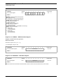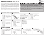
1
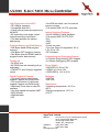
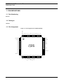
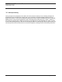
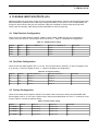
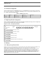
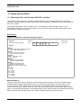
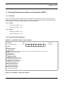
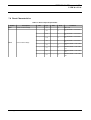
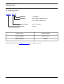
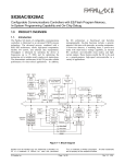
AX2010
User Manual
[AX2010-UM-102-EN]
Rev 1.0.2
January 2012
AppoTech Limited
Add: Unit 705-707, 7/F, IC Development Ctr, No. 6, Science Park West Ave. Hong Kong Science Park, Shatin, N.T. HK
Tel: (852) 2607 4090
Fax: (852) 2607 4096
www.appotech.com
AX2010 8-bit CMOS Micro Controller
High Performance 8-bit MCU
• DC-48MHz operation
• Compatible with 8051
• 104ns internal interrupt response at
48 MIPS
• All instructions are single-cycled
except branching instructions
• Two data pointers for indirect
addressing
Program Memory and Data Memory
• 60K Bytes Mask ROM program
memory
• 32K Bytes OTP program memory
• 34K Bytes internal SRAM used for
program and/or data memory
Flexible I/O
• 28 GPIO pins
• All GPIO pins are internally pull-up
selectable
• CMOS/TTL-level Schmitt triggered
inputs
Digital Peripheral Features
• Two multi-function 8-bit timers,
support Capture and PWM mode
• Two multi-function 16-bit timers,
support Capture and PWM mode
• Watchdog Timer with on-chip RC
oscillator
• One high-speed full-duplex UART
• MP3 decoder
• WMA decoder
• SPI
• One EMI controller, use for external
memory access
• Full-speed USB 2.0 OTG controller
Analog Peripheral Features
• One 4~24MHz Crystal Oscillator
• Full-speed USB 2.0 OTG PHY
• PLL
• DAC
• ADC
• Power-on reset
• Two Low Drop-Out regulators: 5V to
1.8V, 5V to 3.3V
• RC Oscillator
Programming and Debugging Support
• In-System Programming (ISP) support
• In-System Debugging (ISD) support
Power Supply
• LDOVDD is 3.2V to 5.5V
• VDDIO is 3.0V to 3.6V
• VDDCORE is 1.6V to 2.0V
Packages
• LQFP48
• DIE form
Temperature
• Operating temperature: -40°C to
+85°C
• Storage temperature: -65°C to
+150°C
AppoTech Limited
Address
:Unit 705-707, 7/F, IC Development Centre,
No.6, Science Park West Ave.,
Hong Kong Science Park,
Shatin, N.T., Hong Kong
Telephone
:(852) 2607 4090
Fax
:(852) 2607 4096
www.appotech.com
AX2010 8-bit Microcontroller
Rev 1.0.2
USER MANUAL
Table of Contents
1 PIN DEFINITIONS ........................................................................................................................ 4
1.1 Part Numbering........................................................................................................................... 4
1.2 Packages.................................................................................................................................... 4
1.3 Pin Assignment........................................................................................................................... 4
2 MEMORY ORGANIZATION ......................................................................................................... 5
2.1 Special Function Registers......................................................................................................... 5
3 INTERRUPT ................................................................................................................................. 6
3.1 Interrupt Sources and Vectors.................................................................................................... 6
3.2 Interrupt Priority.......................................................................................................................... 6
3.3 Interrupt Latency......................................................................................................................... 8
4 FLEXIBLE INPUTS/OUTPUTS (I/O) ............................................................................................9
4.1 Data Direction Configuration....................................................................................................... 9
4.2 Port Data Configuration.............................................................................................................. 9
4.3 Pull-up Configuration.................................................................................................................. 9
4.4 Pull-down Configuration............................................................................................................ 10
4.5 Digital Input Enable Configuration............................................................................................ 10
4.6 Wakeup..................................................................................................................................... 10
4.6.1 Wakeup through External Port0......................................................................................10
4.6.2 Wakeup Registers........................................................................................................... 11
5 Timers and oscillator ...............................................................................................................12
5.1 Watchdog Timer with On-chip 32KHz RC oscillator..................................................................12
6 Universal Asynchronous Receiver Transmitter (UART) ........................................................13
6.1 Overview................................................................................................................................... 13
6.2 Special Function Registers....................................................................................................... 13
7 Characteristics ......................................................................................................................... 15
7.1 I/O DC Characteristics.............................................................................................................. 15
7.2 MCLR DC Characteristics......................................................................................................... 16
7.3 DAC characteristics.................................................................................................................. 16
7.4 Reset Characteristics................................................................................................................ 17
8 Ordering Code .......................................................................................................................... 18
Appendix I Revision History ......................................................................................................19
© 2011 AppoTech Ltd
3
AX2010 8-bit Microcontroller
Rev 1.0.2
USER MANUAL
1 PIN DEFINITIONS
1.1 Part Numbering
AX2010
1.2 Packages
LQFP48
1.3 Pin Assignment
4
VDDCORE
P06
P07
P20
P21
P22
P23
P24
P25
P26
P27
P10
Figure 1-1: Pin assignment for LQFP48 package
48
47
46
45
44
43
42
41
40
39
38
37
VSSCORE
1
36
VDDIO
VDDIO
2
35
VDDLDO
P41
3
34
VSSIO
P40
4
33
USBDP
P05
5
32
USBDM
P03
6
31
P11
P02
7
30
P12
P01
8
29
P13/DP
P00
9
28
P34
P37
10
27
MCLR /VPP
P36
11
26
P16
VSSDAC
12
25
P17
13
14
15
16
17
18
19
20
21
22
23
24
DACL
VCM
DACR
VDDDAC
VDDIRT
IRTOSCI
IRTOSCO
IRTWKO
P35
P32
P31
P30
AX2010
LQFP48
© 20 11 AppoTech Ltd
AX2010 8-bit Microcontroller
Rev 1.0.2
USER MANUAL
2 MEMORY ORGANIZATION
0x3fff
0x3fff
CODE
XDATA
0x0000
0x0000
2.1 Special Function Registers
The Special Function Registers (SFR) used by the CPU and Peripheral Modules for controlling the desired
operation. The Special Function Registers can be classified into two sets: core and peripheral. Core SFR will
be described in this section. Peripheral SFR will be described in related peripherals.
Register 2-1: PSW - Processor Status Word
PSW
Address
Processor Status Word
0xD0
BANK 0
7
6
5
CY
AC
F1
4
3
RS1 RS0
2
1
0
Default Value
OV
SBS
P
0000 0000
R/W R/W R/W R/W R/W R/W R/W R/W
CY: Carry Flag
AC: Auxiliary carry flag
F1: General purpose flag available for user
RS1, RS0: Register bank select
00: bank0
01: bank1
10: bank2
11: bank3
OV: Overflow flag
SBS: SFR bank select
0: Select SFR bank0
1: Select SFR bank1
P: Odd parity check of ACC
0: There are even number of '1' bits in ACC
1: There are odd number of '1' bits in ACC
© 2011 AppoTech Ltd
5
AX2010 8-bit Microcontroller
Rev 1.0.2
USER MANUAL
3 INTERRUPT
3.1 Interrupt Sources and Vectors
All interrupts, with the exception of the ISD, are controlled by a series combination of individual enable bits
and a global enable (EA) in the interrupt-enable register (IEN0.7). Setting EA to logic 1 allows individual
interrupts to be enabled. Setting EA to logic 0 disables all interrupts regardless of the individual interruptenable settings. The interrupt enables and priorities are functionally identical to those of the 80C52, except
that the AX2010 supports 3 levels of interrupt priorities instead of the original 2.
3.2 Interrupt Priority
There are 3 levels of interrupt priority: Level 2 to 0. The highest interrupt priority is level 2, which is reserved
for the ISD interrupts. All other interrupts have individual priority bits in the interrupt priority registers to allow
each interrupt to be assigned a priority level from 1 to 0. All interrupts also have a natural hierarchy. In this
manner, when a set of interrupts has been assigned the same priority, a second hierarchy determines which
interrupt is allowed to take precedence. The natural hierarchy is determined by analysing potential interrupts
in a sequential manner with the order listed in Table 3-1.
The processor indicates that an interrupt condition occurred by setting the respective flag bit. This bit is set
regardless of whether the interrupt is enabled or disabled.
Table 3-1: Interrupt Summary
Interrupt
Sources
Interrupt Vector
Interrupt
Number
Natural Order
Interrupt Flag
Interrupt Enable Bit
Priority
Control Bit
Timer 0
0x000B / 0x400B
1
2
TMR0CON.7
IE0.1
IP0.1
Timer 1
0x0013 / 0x4013
2
3
TMR1CON.7
TMR1CON.6
IE0.2
IP0.2
Timer 2
0x001B / 0x401B
3
4
TMR2CON.7
TMR2CON.6
IE0.3
IP0.3
Timer 3
0x0023 / 0x4023
4
5
TMR3CON.7
IE0.4
IP0.4
PORT
0x0063 / 0x4063
12
13
WKPND
IE1.5
IP1.5
LVD
0x0073 / 0x4073
14
15
LVDCON.7
IE1.7
IP1.7
WDT
0x0073 / 0x4073
14
15
WDTCON.7
IE1.7
IP1.7
RTCC
0x0073 / 0x4073
14
15
RTCON.7
IE1.7
IP1.7
UART
0x0073 / 0x4073
14
15
UTSTA.5
UTSTA.4
IE1.7
IP1.7
IRTCC
0x0073/0x4073
14
15
IRTCON.3
IRTCON.5
IE1.7
IP1.7
Register 3-1: IEN0 - Interrupt Enable 0 Register
IEN0
Address
Interrupt Enable 0 Register
0xA8
BANK 0
EA: Global Interrupt Enable Bit
0: Disable
1: Enable
T3IE: Timer3 Interrupt Enable Bit
0: Disable
6
7
6
5
4
3
2
1
0
Default Value
EA
-
-
T3IE
T2IE
T1IE
T0IE
-
0000 0000
R/W
R/W
R/W
R/W R/W R/W
R/W R/W
© 20 11 AppoTech Ltd
AX2010 8-bit Microcontroller
Rev 1.0.2
USER MANUAL
1: Enable
T2IE: Timer2 Interrupt Enable Bit
0: Disable
1: Enable
T1IE: Timer1 Interrupt Enable Bit
0: Disable
1: Enable
T0IE: Timer0 Interrupt Enable Bit
0: Disable
1: Enable
Register 3-2: IEN1 - Interrupt Enable 1 Register
IEN1
Address
Interrupt Enable 1 Register
0xA9
BANK 0
7
6
5
4
3
2
1
0
Default Value
UIE
-
PORT
IE
-
-
-
-
-
0000 0000
R/W
-
R/W
R/W R/W R/W
R/W R/W
UIE: LVD / UART/WDT Interrupt Enable Bit
0: Disable
1: Enable
PORTIE: Port Wakeup Interrupt Enable Bit
0: Disable
1: Enable
Register 3-3: IP0 - Interrupt Priority 0 Register
IP0
Address
7
6
5
4
3
2
1
0
Default Value
Interrupt Priority 0 Register
0xB8
-
-
-
T3IP
T2IP
T1IP
T0IP
-
- 000 0000
-
R/W
BANK 0
R/W R/W
R/W R/W
R/W R/W
T3IP: Timer3 Interrupt Priority Select
0: Low 1: High
T2IP: Timer2 Interrupt Priority Select
0: Low 1: High
T1IP: Timer1 Interrupt Priority Select
0: Low 1: High
T0IP: Timer0 Interrupt Priority Select
0: Low 1: High
Register 3-4: IP1 - Interrupt Priority 1 Register
IP1
Address
Interrupt Priority 1 Register
0xB9
BANK 0
7
6
5
4
3
2
1
0
Default Value
UIP
-
POR
TIP
-
-
-
-
-
0000 0000
R/W
R/W
R/W R/W
R/W R/W
R/W R/W
UIP: LVD / UART/WDT Interrupt Priority Select
0: Low 1: High
PORTIP: Port Wakeup Interrupt Priority Select
0: Low 1: High
© 2011 AppoTech Ltd
7
AX2010 8-bit Microcontroller
Rev 1.0.2
USER MANUAL
3.3 Interrupt Latency
Interrupt response time depends on the state of the CPU when the interrupt occurs. Pending interrupts are
sampled and priority decoded each system clock cycle. Therefore, the fastest possible response time is 4
system clock cycles: 1 clock cycle to detect the interrupt and 3 clock cycles to complete the LCALL to the ISR.
Additional clock cycles will be required if the CPU is executing branch instructions (e.g.: ACALL, LJMP, JZ...).
If an interrupt is pending when a RETI is executed, a single instruction is executed before an LCALL is made
to service the pending interrupt. If the CPU is executing an ISR for an interrupt with equal or higher priority, the
new interrupt will not be serviced until the current ISR completes, including the RETI and following instruction.
8
© 20 11 AppoTech Ltd
AX2010 8-bit Microcontroller
Rev 1.0.2
USER MANUAL
4 FLEXIBLE INPUTS/OUTPUTS (I/O)
AX2010 provides four ports (Port 0/1/2/3) for user to develop applications. Inputs are all Schmitt triggered with
about 400-500mV hysteresis level to filter input voltage fluctuations. Each port pin can be independently set
as input or output. Most of the port pins are built-in slew-rate controlled to reduce output bouncing noise.
There is also an internally 10KΩ pull-up resistor selectable for each input port pin.
4.1 Data Direction Configuration
There are four port data direction registers: P0DIR, P1DIR, P2DIR, P3DIR. All port pins are defined as
“output” when it is set as “0” and as “input” when it is set as “1”. Table 4-1 illustrates the configuration.
Table 4-1: PxDIR registers setting
Register
Address
Set bit “x” of PxDIR as “1”
Clear bit “x” of PxDIR as “0”
Initial value
P0DIR
BAh
Inputs
Outputs
FFh
P1DIR
BBh
Inputs
Outputs
FFh
P2DIR
BCh
Inputs
Outputs
FFh
P3DIR
BDh
Inputs
Outputs
FFh
4.2 Port Data Configuration
There are four port data registers: P0, P1, P2, P3. The port data value is stored as “0” when Px register is set
to “0” and as “1” when Px register is set to “1”. Table 4-2 illustrates the configuration.
Table 4-2: Px registers setting
Register
Address
Set bit x of Px as “1”
Clear bit x of Px as “0”
Initial value
P0
80h
Stored “1”
Stored “0”
xx
P1
90h
Stored “1”
Stored “0”
xx
P2
A0h
Stored “1”
Stored “0”
xx
P3
B0h
Stored “1”
Stored “0”
xx
4.3 Pull-up Configuration
There are four data pull-up registers: P0UP, P1UP, P2UP, P3UP. The port pin will be pull-up disabled when
PxUP register is set to “0” or the pin is set as output, and pull-up enabled when it is set to “1” and the pin is set
as input. Table 4-3 shows the register setting.
Table 4-3: PxUP register setting
Register
Address
Set as “1”
Clear as “0”
Initial value
P0UP(BANK 1)
BAh
Enable pull-up
Disable pull-up
00h
P1UP(BANK 1)
BBh
Enable pull-up
Disable pull-up
08h
P2UP(BANK 1)
BCh
Enable pull-up
Disable pull-up
00h
P3UP(BANK 1)
BDh
Enable pull-up
Disable pull-up
00h
© 2011 AppoTech Ltd
9
AX2010 8-bit Microcontroller
Rev 1.0.2
USER MANUAL
4.4 Pull-down Configuration
There are 2 data pull-down bit: SPMODE[0] for pin P1.7 and SPMODE[1] for pin P3.7 and P0.6. The port pin
will be pull-down disabled when SPMODE[0] or SPMODE[1] is set to “0” and pull-down enabled when it is set
to “1”. Table 4-4 shows the register setting.
Table 4-4: SPMODE register setting
Bit
Address
Set as “1”
Clear as “0”
Initial value
SPMODE.0
AEh
Enable pull-down
Disable pull-down
1
SPMODE.1
AEh
Enable pull-down
Disable pull-down
1
4.5 Digital Input Enable Configuration
There is 1 digital input enable register: PIE. There are several I/O MUXed with analog module. I/O digital input
and output must be disabled when Analog Module is enabled.
Register 4-1: PIE – Port Digital Input Enable
PIE
Address
Port Input Enable
0x9A
BANK 0
7
6
PIE7
R/W
5
4
3
2
1
0
Default Value
PIE6
PIE3
PIE2
PIE1
PIE0
11 - - 1111
R/W
R/W
R/W
R/W
R/W
PIE7: P35 and P37 Digital Input Enable Bit (For AMUX )
0 = P35 and P37 Input Disabled
1 = P35 and P37 Input Enabled
PIE6: P34 and P36 Digital Input Enable Bit (For AMUX)
0 = P34 and P36 Input Disabled
1 = P34 and P36 Input Enabled
PIE3: P03 Digital Input Enable Bit (For ADC3)
0 = P03 Input Disabled
1 = P03 Input Enabled
PIE2: P02 Digital Input Enable Bit (For ADC2)
0 = P02 Input Disabled
1 = P02 Input Enabled
PIE1: P01 Digital Input Enable Bit (For ADC1)
0 = P01 Input Disabled
1 = P01 Input Enabled
PIE0: P00 Digital Input Enable Bit (For ADC0 or LVD external input)
0 = P00 Input Disabled
1 = P00 Input Enabled
4.6 Wakeup
4.6.1 Wakeup through External Port0
Wakeup is one way of causing the device to exit the power down mode. AX2010 supports Port Wakeup. The
PWKEN registers (Wakeup Enable Register) allow P0.4, P0.5, P0.6 and P0.7 to cause wakeup.
Clearing bit0-3 in the PWKEN register enables wakeup on corresponding pin of P0.4, P0.5, P0.6 and P0.7.
The trigger condition on the selected pin can be either rising edge or falling edge. The WKED register
(Wakeup Edge Select) selects the desired transition edge. Setting a bit in WKED register selects the falling
edge of the corresponding P0.4, P0.5, P0.6 and P0.7 pin. Resetting the bit selects the rising edge. The
PWKEN registers are set to 0Fh upon reset.
10
© 20 11 AppoTech Ltd
AX2010 8-bit Microcontroller
Rev 1.0.2
USER MANUAL
Once a valid transition occurs on the selected pin, the WKPND(PWKEN.7~PWKEN.4) register (Wakeup
Pending Register) latches the transition in the corresponding bit position. Logic ‘1’ indicates the occurrence of
the selected trigger edge on the corresponding Port pins. Upon reset, logic ‘0’ is set to all bits of WKPND.
Note:
1. Port 0 Wakeup initialization, To avoid any false signalling to port, the followings would be a recommended
procedure for Wakeup initialization:
•
Configure the edge select of Port 0 pins on WKEDG register,
•
Clear the corresponding bits on WKPND Wakeup Pending Register
•
Clear the corresponding bits in the PWKEN registers to enable the wakeup on the
corresponding port pins
2. Upon exiting the sleep down mode, the Multi-Input Wakeup logic causes full chip reset.
4.6.2 Wakeup Registers
Register 4-2: PWKEN – Port 0 Wakeup Enable Register
PWKEN
Port 0 Wakeup Enable Register
Address
0x98
BANK 0
7
6
5
4
3
2
1
0
Default Value
WKP
ND3
WKP
ND2
WKP
ND1
WKP
ND0
PWK
EN3
PWK
EN2
PWK
EN1
PWK
EN0
0000 1111
R/W R/W R/W R/W R/W R/W R/W R/W
WKPNDx
0 = No port0.x wakeup event occurred
1 = Port0.x wakeup event occurred
PWKENx
0 = Enable Port0.x Wakeup
1 = Disable Port0.x Wakeup
Note:
1.
2.
3.
4.
Enable Port0.x Wakeup is a condition of Port0.x wakeup events occurred.
To enable WKPNDx, set PWKENx to '0'.
To clear WKPNDx, write '0' to WKPNDx. WKPNDx will be '0' 2 clocks later after write '0' to WKPNDx.
WKPNDx is cleared when PWKENx is '1'.
Register 4-3: PWKEDGE – Port 0 Wake up Event Select
PWKEDGE
Address
7
6
5
4
3
2
1
0
Default Value
Port 0 Wake up Event Select
0x99
-
-
-
-
WKE
DG3
WKE
DG2
WKE
DG1
WKE
DG0
- - - - xxxx
BANK 0
R/W R/W R/W R/W
WKEDGx: Port Wake up Edge Select
0 = select rising edge as wake up event
1 = select falling edge as wake up event
© 2011 AppoTech Ltd
11
AX2010 8-bit Microcontroller
Rev 1.0.2
USER MANUAL
5 Timers and oscillator
5.1 Watchdog Timer with On-chip 32KHz RC oscillator
The Watchdog Timer (WDT) logic consists of a 20bit Watchdog Timer. The Watchdog Timer is clocked by
internal RC oscillator running at 32KHz. When device resets, the WDT is disabled and user should enable the
WDT if it is needed.
In the default configuration, WDT overflows in 2 ms. The application program needs to write a '1' into
WDTCON[5] at least once 2 ms to prevent WDT time out. The lower 3 bits of the WDTCON register control
the selection of overflow time period.
WDT Registers
Register 5-1: WDTCON – Watchdog Configure Register
WDTCON
Address
Watchdog Configure Register
0xF7
BANK 0
7
6
5
4
3
WDTT
O
WDTP
D
CLR
WDT
WDT
EN
RSTE
N
R/W
2
1
0
WDTPS
Default Value
0000 0000
R/W WO R/W R/W R/W R/W R/W
WDTTO:
0 = Read '0' after clear Watchdog or Power up
1 = Read '1' after Watchdog time out
WDTPD:
0 = read '0' before sleep operation
1 = read '1' after sleep operation
CLRWDT:
Write 1 : Clear WDT counter
Write 0 : No action
WDTEN:
0 = Disables the Watchdog timer
1 = Enables the Watchdog timer
RSTEN:
0 = Disables the Watchdog reset
1 = Enables the Watchdog reset
WDTPS: WDT time out period setting
000 : 2ms
001 : 8ms
010 : 32ms
011: 128ms
100 : 512ms
101: 2048ms
110 : 8192ms
111 : 32768ms
Watchdog Wake up
There are 2 modes for wake up operation: wake up without reset and wake up with reset. It determines by
RSTEN bit (WDTCON[3]). When RSTEN sets to 0, the watchdog will generate a non-reset wake up after
counter overflows. Only in HOLD Mode, non-reset wake up can wakeup AX2010 and it will continue to
execute next instruction. AX2010 cannot be waken up by WDT without reset in SLEEP Mode. When RSTEN
sets to 1, the watchdog will generate a reset wakeup after counter overflows. Both in HOLD Mode and SLEEP
Mode, watchdog reset can wake up the chip, and then, AX2010 goes back to the initial state.
12
© 20 11 AppoTech Ltd
AX2010 8-bit Microcontroller
Rev 1.0.2
USER MANUAL
6 Universal Asynchronous Receiver Transmitter (UART)
6.1 Overview
UART is a serial port capable of asynchronous transmission. The UART can function in full duplex mode.
Receive data is buffered in a holding register. This allows the UART to start reception of a second incoming
data byte before software has finished reading the previous data byte.
When U1SRC = 0
•
Receive pin (U1RX) – P0.6
•
Transmit pin (U1TX) – P1.6
When U1SRC = 1
•
Receive pin (U1RX) – P3.7
•
Transmit pin (U1TX) – P3.5
6.2 Special Function Registers
Register 6-1: UARTCON – UART Configure Register
UARTCON
Address
UART Configure Register
0xFD
BANK 0
7
6
5
4
3
2
1
0
Default Value
UTSB
S
UTTX
NB
NBIT
EN
UTE
N
UTTXI
NV
UTRX
INV
TXIE
RXIE
0100 0000
R/W
R/W R/W R/W R/W R/W R/W R/W
UTSBS: Stop Bit Select
0 = 1 bit as Stop Bit
1 = 2 bits as Stop Bit
UTTXNB: The ninth bit data of transmitter buffer. Write the ninth bit into this location that you want to transmit
NBITEN: Nine-BIT mode Enable Bit
0 = Eight-bit mode
1 = Nine-bit mode
UTEN: UART Enable Bit
0 = Disable UART module
1 = Enable UART module
UTTXINV: Transmit Invert Selection Bit
0 = Transmitter output without inverted
1 = Transmitter output inverted
UTRXINV: Receive Invert Selection Bit
0 = Receiver input without inverted
1 = Receiver input inverted
TXIE: Transmit Interrupt Enable
0 = Transmit interrupt disable
1 = Transmit interrupt enable
RXIE: Receive Interrupt Enable
0 = Receiver interrupt disable
1 = Receiver interrupt enable
Register 6-2: UARTSTA – UART Status Register
© 2011 AppoTech Ltd
13
AX2010 8-bit Microcontroller
Rev 1.0.2
USER MANUAL
UARTSTA
UART Status Register
Address
0xFC
BANK 0
7
6
5
4
3
2
1
0
Default Value
UTRX
NB
FEF
U1R
XIF
U1TX
IF
-
-
-
U1SR
C
xx01 - - -0
R/W
R/W R/W R/W
-
-
-
R/W
3
2
1
UTRXNB: The ninth bit data of receiver buffer
FEF: Frame Error Flag
0 = the stop bit is '1' in the last received frame
1 = the stop bit is '0' in the last received frame
U1RXIF: UART RX Interrupt Flag
0 = UART receive not done
1 = UART receive done
U1TXIF: UART TX Interrupt Flag
0 = UART transmit not done
1 = UART transmit done
Writing a data to UTBUF or 0 to U1TXIF to clear this flag.
U1SRC: UART Source Select
0 = UART select
P0.6 as receive pin
P1.6 as transmit pin
1 = UART select
P3.7 as receive pin
P3.5 as transmit pin
Register 6-3: UTBAUD – UART Baud Rate Register
Register of UART baud rate generator
Baud rate formula:
Baud Rate =f system clock / [ 8 ( n + 1 )]
(n is 8-bit Register, range 0~256)
UARTBAUD
Address
UART Baud Rate Register
0xFE
BANK 0
7
6
5
4
0
UARTBAUD
Default Value
xxxx xxxx
R/W R/W R/W R/W R/W R/W R/W R/W
Register 6-4: UARTDATA – UART Data Register
UARTDATA
Address
UART Data Register
0xFF
BANK 0
7
6
5
4
3
2
1
0
UARTDATA
Default Value
xxxx xxxx
R/W R/W R/W R/W R/W R/W R/W R/W
Write this location will load the data to transmitter buffer, read this location will read the data from the receiver buffer.
14
© 20 11 AppoTech Ltd
AX2010 8-bit Microcontroller
Rev 1.0.2
USER MANUAL
7 Characteristics
7.1 I/O DC Characteristics
Table 7-1: I/O input DC voltage parameters
Symbol
Descriptions
Min
Typ
Max
Units
Conditions
VIL
Low-Level Input Voltage
-
-
30% * VDDIO
V
VDDIO = 3.3V
VIH
High-Level Input Voltage
70% * VDDIO
-
-
V
VDDIO = 3.3V
Low-level input voltage (VIL) is the threshold voltage read as logic “0”. Higher than VIL may not read as “0”.
For the difference between devices (or pins), the VIL are different, so all the design should refer to the actual
criterion.
High-level input voltage (VIH) is the threshold voltage read as logic “1”. Lower than VIH may not read as “1”.
For the difference between devices (or pins), the VIH are different, so all the design should refer to the actual
criterion.
© 2011 AppoTech Ltd
15
AX2010 8-bit Microcontroller
Rev 1.0.2
USER MANUAL
7.2 MCLR DC Characteristics
Table 7-2: MCLR input DC voltage parameters
Symbol
Descriptions
Min
Typ
Max
Units
Conditions
VMIL
MCLR Low-Level Input
Voltage
-
0.2*VDDIO
-
V
VDDIO = 3.3V
VMIH
MCLR High-Level Input
Voltage
-
0.8*VDDIO
-
V
VDDIO = 3.3V
Table 7-3: MCLR input AC voltage parameters
Symbol
Descriptions
TMCLR
Min
Typ
MCLR Low-Level Input width 1
-
Max
-
Units
ms
Conditions
VDDIO = 3.3V
Table 7-2 shows MCLR circuit configuration. Capacitance (C1) is modified to change circuit’s parameter.
VDDIO = 3.3 V
MCLR PAD
To system
R1 = 10Kohm
C1 = 104
Figure 7-1: MCLR circuit configuration
7.3 DAC characteristics
Table 7-4: DAC characteristics
Symbol
Descriptions
Min
Typ
Max
Units
SNR
-
85
-
db
Total Harmonic Distortion+Noise
-
80
-
db
DR(Dynamic Range)
-
86
-
db
3.0
3.3
3.6
V
-
5.89
-
mA
51
600
nA
Conditions
Characteristics
Power Specifications
Analog supply
Power Supply Current
Sleep Current
16
© 20 11 AppoTech Ltd
AX2010 8-bit Microcontroller
Rev 1.0.2
USER MANUAL
7.4 Reset Characteristics
Table 7-5: Reset output AC parameters
Symbol
Vpor
Vlvdr
Descriptions
Power On Reset Voltage
Min
Typ
Max
Units
-
1.2
-
V
VDD= 3.3V
-
2.2
-
V
EX_PIN,VDDIO = 3.3V LVDS =
11
-
2.05
-
V
EX_PIN,VDDIO = 3.3V LVDS =
10
-
1.95
-
V
EX_PIN,VDDIO = 3.3V LVDS =
01
-
1.8
-
V
EX_PIN,VDDIO = 3.3V LVDS =
00
-
3.3
-
V
VDDLDO,VDDIO = 3.3V LVDS
= 11
-
3.1
-
V
VDDLDO,VDDIO = 3.3V LVDS
= 10
-
2.9
-
V
VDDLDO,VDDIO = 3.3V LVDS
= 01
-
2.7
-
V
VDDLDO,VDDIO = 3.3V LVDS
= 00
LVD Out Reset Voltage
© 2011 AppoTech Ltd
Conditions
17
AX2010 8-bit Microcontroller
Rev 1.0.2
USER MANUAL
8 Ordering Code
Part No – S S S
Packing:
T = Tray form
Package:
DE6 = Bare DIE, thickness 11mil
LQ1 = LQFP, Lead count 48
Device Option:
QAA = OTP Blank
Device:
AX2010
Ordering Code
Brief Description
AX2010-QAADE6T
Bare Die 11mil
AX2010-QAALQ1T
LQFP48
Please contact sales office ([email protected]) for ordering procedures.
18
© 20 11 AppoTech Ltd
AX2010 8-bit Microcontroller
Rev 1.0.2
USER MANUAL
9 Appendix I Revision History
Date
Version
Comment
Revised by
2011-08-29
1.0.1
Updated document format
Erica Cheong
2012-01-17
1.0.2
Changed new logo
Added ordering code
Erica Cheong
The information in this document is believed to be accurate in all respects at the time of publication but is subject to change without
notice. AppoTech assumes no responsibility for errors and omissions, and disclaims responsibility for any consequences resulting
from the use of information included herein. Additionally, AppoTech assumes no responsibility for the functioning of undescribed
features or parameters. AppoTech reserves the right to make changes without further notice. AppoTech makes no warranty,
representation or guarantee regarding the suitability of its products for any particular purpose, nor does AppoTech assume any
liability arising out of the application or use of any product or circuit, and specifically disclaims any and all liability, including without
limitation consequential or incidental damages. AppoTech products are not designed, intended, or authorized for use in applications
intended to support or sustain life, or for any other application in which the failure of the AppoTech product could create a situation
where personal injury or death may occur. Should Buyer purchase or use AppoTech products for any such unintended or
unauthorized application, Buyer shall indemnify and hold AppoTech harmless against all claims and damages.
In case of any questions or comments about this documentation, please feel free to contact AppoTech at
[email protected].
© 2011 AppoTech Ltd
19