1
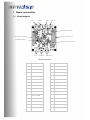
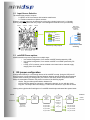
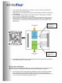
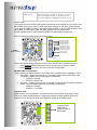
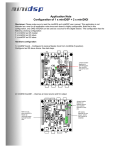
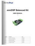
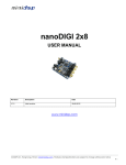
miniDIGI I/O card
USER MANUAL
V1.3
Revision
Description
Date
V1.0
User manual – Initial version
25-02-2010
V1.1
Updated section on Digital/Analog toggle switch
05-05-2010
V1.2
Updated diagrams for I2S section
02-06-2010
V1.3
Updated general descriptions
01-02-2011
1 Board connectivity
1.1
Board diagram
Toslink 1
Toslink 2
SPDIF 2
SPDIF 1
Source selection header
Expansion connector J16
Expansion connector J2
Master/Slave jumper
I2S channel selection header
DC in
SPDIF OUT
Optical OUT
Expansion Connector J16
Pin
Description
Pin
Description
1
n/a
2
n/a
3
n/a
4
n/a
5
Ground
6
Ground
7
Ground
8
Ground
9
MCLKIN
10
I2S_DATA_IN1&2
11
I2S_DATA_IN3&4
12
I2S_DATA_IN5&6
13
I2S_DATA_IN7&8
14
I2S_IN_LRCLK
15
I2S_IN_BCLK
16
I2S_DATA_OUT1&2
17
I2S_DATA_OUT3&4
18
I2S_DATA_OUT5&6
19
IS2_DATA_OUT7&8
20
I2S_OUT_LRCLK
21
I2S_OUT_BCLK
22
3.3V
23
n/a
24
3.3V
25
GND
26
GND
27
n/a
28
n/a
1.2
Input Source Selection
The miniDIGI has a total of 4 inputs:
- 2 x SPDIF on RCA connectors with isolation transformers
- 2 x Toslink connection on Optical receivers
However, only one signal can be selected at a time using a single jumper on a 2 x 4 header.
Warning that placing more than one jumper could damage the board and void your warranty.
Toslink#1
Toslink#2
SPDIF#1
SPDIF#2
BBM switch
toggling between
SPDIF1/2
Toslink 1/2
Select one of the inputs
SPDIF #1
SPDIF #2
Toslink #1
Toslink #2
Zoomed up with jumpers
1.3
Break Before Make
switching
miniDIGI Power options
miniDIGI boards may receive power from multiple ways:
o In a stacked configuration, from another miniDSP board powered by USB.
o In a stacked configuration, from another miniDSP or miniAMP powered by DC
supply
o Locally, a DC connector can be soldered to the board with an external supply
ranging from 4.5 to 24VDC
2 I2S jumper configuration
Configuration flexibility is a core design feature of the miniDSP concept. Using the I2S (Inter IC
Sound) protocol, synchronized data is shared between between boards. Besides the advantages
of better noise immunity (vs analog audio), the choice of the widely known I2S protocol allows
design & customization freedom. I2S protocol consists of the following signals:
- Clocks: They provides synchronization between ICs
- I2S_IN: I2S input data lines carrying 2 x 24bit audio channels, in sync with the clocks
- I2S_OUT: I2S output data lines carrying 2 x 24bit audio channels, in sync with the clocks
Looking at the typical audio flow diagram of a miniDIGI board helps understand the system better:
INPUTS
SPDIF#1/2
Toslink#1/2
1
2
3
4
5
Source
selection
header
Digital
Audio
Receiver
Sample
Rate
Converter
I2S header
Source
Selection
Digital
Audio
Transmitter
Selection of
one of the
input source
I2S_IN
I2S_IN
I2S_IN
I2S_IN
ch1&2
ch3&4
ch5&6
ch7&8
Routing of
1xI2S_in
&
1xI2S_out
I2S_OUT
I2S_OUT
I2S_OUT
I2S_OUT
OUTPUTS
ch1&2
ch3&4
ch5&6
ch7&8
SPDIF#1
Toslink#1
1. Audio inputs (SPDIF/TOSLINK) are connected to a source selection header where the
user can select 1 out of the 4 sources.
2. Signal is then fed to the Digital Audio Receiver which translates the SPDIF/Toslink signal
to an I2S signal
3. The sample rate converter (SRC) is next in line to insure the input signal is compatible
with the miniDSP configured sample rate (48kHz)
4. The next step is the I2S routing, i.e. the routing of a digital signal to the I2S bus shared
between boards in a stacked configuration (link cables). As shown in the diagram below,
using jumpers, one can decide to route the I2S data signal on any I2S channels of the
expansion bus.
SPDIF or Toslink
Input
SPDIF or Toslink
Input
Jumper selects which
I2S channel the
SPDIF input signal is
being routed to.
Jumper selects
which I2S channel
the SPDIF output
receives.
5. Finally, I2S_OUT jumpers allow you to configure which channel you want to convert from
I2S to SPDIF/Toslink if it is ever required.
Step by Step configuration
Please pay attention to the following diagram to clearly understand how to route your data to the
correct pin. Incorrect configuration could create a short circuit and damage your board.
1. The first step consists in reading the plug-in datasheet to figure out which I2S channels
will be available from the miniDSP kit. This information is useful to understand how
external I/O cards can link up to the miniDSP kit. Taking for example the Crossover plugin, you can read in the technical specification section:
Digital Inputs
Digital Outputs
Plug-in IN#1&2 selectable on I2S_Data_In7&8
Plug-in OUT#1/2/3/4 available on I2S_Data_Out1/2/3/4
Un-processed signal from ADC on I2S_Data_Out5/6
Un-processed signal from Digital IN on I2S_Data_Out 7/8
In other words:
- If you want to send the SPDIF input signal for processing on the miniDSP kit, you need to route
the miniDIGI to the plug-in inputs, in other words place a jumper on I2S_Data_in7&8 channels
- If you want OUT#3&4, post plug-in processing by the miniDSP, to be converted to SPDIF out on
the miniDIGI, you will need to “grab” I2S_Data_Out3&4 from the expansion bus.
See the example below for exact location of jumpers for that template configuration.
Here is a zoomed up version of the I2S routing header:
Using jumpers, route the I2S data to the correct channel.
3
Outputs
2
1
0
Inputs
3
2
1 0
Master/
Slave Jumper
I2S_Data_IN_ch7&8
I2S_Data_IN_ch5&6
I2S_Data_IN_ch3&4
I2S_Data_IN_ch1&2
I2S_Data_OUT_ch7&8
I2S_Data_OUT_ch5&6
I2S_Data_OUT_ch3&4
I2S_Data_OUT_ch1&2
Always closed for
SCLK & LRCLK
MCLK selection
Jumper symbol:
To prevent potential damage with short-circuits, these rules should be followed at all times:
- Select only one SPDIF/Toslink source from the input source selection header
- Select only one I2S_Data_OUT lines on the I2S routing header
I2S Master/Slave configuration
To allow stacking of multiple boards on top of each other, miniDIGI have the capability to run as:
• I2S master – Jumper removed (open): The board outputs clocks (LRCK/SCLK). This
configuration applies to the following board combinations:
o miniDIGI + miniAMP
o miniDIGI + external D/A
• I2S slave – Jumper in place (closed): The board receives clocks from another I2S device
master. This configuration applies to the following combinations:
o miniDIGI + miniDSP
o miniDIGI + 2 x miniDSP
Loopback mode
miniDIGI board can be configured in a loop-back mode for either SPDIF de-jittering or daisy
chaining of multiple miniDIGI boards. A single jumper placed vertically between inputs and
outputs is all you need to link-up the incoming SPDIF stream to the SPDIF output.
3
1
Outputs
2
0
2
Inputs
3
Loop back mode
enabled when
jumper in place at
this location.
1 0
Note that in a loop back mode, audio will effectively go through 2 x miniDIGI and
introduce 2.88ms of delay in the path. In other words, all outputs of the first board will
need to be delayed by 2.88ms to make sure audio is correctly time aligned.
miniDSP 1
SPDIF
Input
miniDSP 2
SPDIF
loop back
miniDIGI 1
miniDIGI 2
Delay all outputs
of this stack only
minDIGI template configurations
miniDIGI may be configured in a multitude of ways and the following configurations are only some
illustrations of the board’s potential.
Option 1: Quick configuration
To simplify your task, summarized jumper charts can be downloaded from the Download section
of our website
o 2 way configuration jumper charts
o 3/4way configuration jumper charts
Option 2: Advanced configuration
For those of you who want to understand more about what they are doing, the following board
stacking configuration will illustrate some typical jumper configurations.
Stereo 2 Way configuration
3
1
Outputs
2
Digital signal
Analog signal
0
miniDIGI
SPDIF/Toslink
Un-Processed signal
2
Inputs
To
amplifier
3
miniDSP
1 0
SPDIF/
Toslink
Option1
In a very similar configuration as above setup,
but this time two miniDIGI boards are linked up
together with an SPDIF link. With this creative
configuration, a single miniDSP is able to power
2 miniAMP + miniDIGI configurations for a truly
digital solution!
Template Jumper configuration:
Stereo 2 Way configuration
To
Speakers
miniAMP
#1
miniAMP
#2
miniDSP
SPDIF/
Toslink
miniDIGI
#1
Link Up
SPDIF
In this stereo 2way configuration, Audio comes
from the SPDIF input on the miniDIGI board.
miniDIGI I2S audio SPDIF input was routed to
I2S_Data_IN_ch7&8 by placing the jumper in
the correct location (Jumper location 0)
The Analog outputs of the miniDSP are being
sent to a multi-channel amplifier for each way.
For future expansion (or linking to another
device), the miniDIGI was also configured to
loop back mode to output the de-jittered SPDIF
signal to another device. Please see the note
below about miniDIGI loop back mode.
To
Speakers
miniDIGI #1 (SPDIF in -> I2S_Data_IN_ch7&8)
miniDIGI #1 (I2S_Data_OUT_ch3&4 - > SPDIF OUT)
miniDSP #1 (Slave Clock, configured for I2S source in plug-in)
miniAMP #1 (I2S_Data_OUT_ch1&2)
miniDIGI #2 (Loop-back mode + Jumper I2S_Data_OUT_ch7&8)
miniAMP #2 (I2S_Data_OUT_ch7&8)
miniDIGI
#2
Please see the note below the loop back mode.
Stereo 4 Way configuration
RIGHT
LEFT
SPDIF/
Toslink
miniDSP
#1
4 ch
Amplifier
miniDSP
#2
miniDIGI
#1
SPDIF/Toslink
miniDIGI
#2
4 ch
Amplifier
Finally, this stereo 4 way configuration displays
a Left & Right active speaker configuration
where 4ch amplifiers or miniAMP modules may
be used to build an all digital configuration.
Template Jumper configuration:
miniDIGI #1 (SPDIF in -> I2S_Data_IN_ch7&8)
miniDIGI #1 (Loop-back for un-processed audio to SPDIF out)
miniDSP #1 (Slave Clock, configured for I2S source in plug-in)
miniAMP #1 (I2S_Data_OUT_ch1&2 + I2S_Data_OUT_ch3&4)
miniDIGI #2 (SPDIF in -> I2S_Data_IN_ch7&8)
miniDSP #2 (Slave Clock, configured for I2S source in plug-in)
miniAMP #2 (I2S_Data_OUT_ch1&2 + I2S_Data_OUT_ch3&4)
Digital / Analog source selection via toggle switch
Control of I2S vs Analog source selection is performed from a radio button inside the miniDSP
plug-in (read miniDSP user manual for more information). Using the I2S data lines, it’s however
possible to toggle between the Analog inputs of the miniDSP and Digital inputs of the miniDIGI
with the following work around. Here are the steps to follow:
- Configure the miniDSP plug-in to I2S input. On all miniDSP plug-ins, this means that
audio needs to be fed to I2S_DATA_IN7&8 pins for processing by the miniDSP
- Knowing that the un-processed signal from the ADC of a miniDSP is also available on
I2S_DATA_IN5&6, we can toggle between analog (from the ADC on miniDSP) and
Digital (from the miniDIGI) with a toggle switch located as below diagram:
3
1
Outputs
2
SPDIF
0 3
1
Inputs
2
ADC
Toggle
Switch
0
Note that toggling between 2 modes should either be done with power OFF or using “Brake
before Make” switches to prevent any potential short circuits.
Troubleshooting
The following symptoms were found to be the most likely cause of issues.
Item#
Symptoms
Troubleshooting recommendation
1
No audio on outputs
2
miniDSP LED not
flashing
2
High Frequency
noise on signal
Contact
Us
Problem unsolved by
above suggestions
Check your jumper configuration carefully:
- I2S source selection
- I2S routing configuration
In 90% of cases, mis-configured jumper
configuration will explain lack of audio
In a stacked configuration with a miniDSP,
make sure to configure the miniDSP board to
Slave Clock (see manual) to be able to receive
the master clock from the miniDIGI board
This is a typical symptom of an incorrectly
configured MCLK (Master/Slave) on a miniDSP
and miniDIGI configuration. Please make sure
to double check the jumper chart for the correct
configuration.
- Have a look at our forums to see if someone
else already had this issue.
- Send us an email ([email protected]) with a
clear explanation of the symptoms and
descriptions of the troubleshooting steps you
already followed. A picture of the jumper
configuration is worth a thousand words…
If not
solved go
to item
Contact us
Contact us
n/a
n/a