1
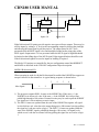
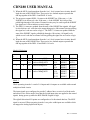
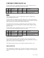
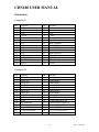
CDN180
USER MANUAL
CDN180 USER MANUAL
TABLE OF CONTENTS
OVERVIEW....................................................................................................................................................1
MOUNTING ...................................................................................................................................................1
POWER ...........................................................................................................................................................2
CAN Interface..................................................................................................................................................2
RESET.............................................................................................................................................................2
LEDS ...............................................................................................................................................................3
SWITCH INPUTS...........................................................................................................................................3
DIGITAL I/O...................................................................................................................................................4
PERIOD MEASUREMENT INPUTS ............................................................................................................7
ANALOG INPUTS .........................................................................................................................................7
PWM OUTPUTS ............................................................................................................................................8
SPI A/D ...........................................................................................................................................................8
SPI D/A ...........................................................................................................................................................8
DEVICENET MODEL....................................................................................................................................8
CCO SUPPORT ..............................................................................................................................................8
Connectors.....................................................................................................................................................10
Connector P1 .........................................................................................................................................10
Connector P2 .........................................................................................................................................10
Appendix A....................................................................................................................................................11
Please Note:
MKS Instruments provides these documents as the latest version for the revision indicated.
The material is subject to change without notice, and should be verified if used in a critical
application.
i
Rev 1.1 9/29/00
CDN180 USER MANUAL
OVERVIEW
The CDN180 DeviceNet Cube provides support for a wide range of analog and digital
interfaces. The preprogrammed device provides a Group II Only device interface in a
convenient, pre-packaged module, greatly simplifying the task of designing custom
DeviceNet compatible nodes.
The 2” X 3” module connects to a user supplied interface board through two 30 pin
headers. Four mounting holes allow physical attachment to the board. An on-board DCDC converter is available to generate 5 volts from the DeviceNet 11-24 Vdc BUS +/signals. The Bus interface includes reverse polarity and loss of ground protection.
Firmware support includes digital inputs, digital outputs, analog inputs, analog outputs, a
user defined configuration object and a CCO programming environment. The device may
be used as a conventional I/O node with a user defined mix of digital and analog I/O or as
a self contained control node.
MOUNTING
The CDN180 is designed to be mounted to a user supplied interface board. Electrical
connections are made through two 30 pin header assemblies. Four mounting screws may
be used for mechanical support.
The CDN180-1 will mate with a wide variety of 30 pin header sockets. SAMTEC part
#SLW-115-01-G-D will provide a low profile connector solution.
The CDN180 uses longer header pins to allow SMD components to be mounted on the
user supplied interface board below the CDN180. SAMTEC part #SSQ-115-01-G-D will
provide a .335 inch clearance.
1
Rev 1.1 9/29/00
CDN180 USER MANUAL
POWER
The CDN180 operates from a +5 Vdc +/- 10%, 50 mA supply. An on board DC to DC
converter is provided which will provide +5 Vdc +/- 5%, 200 mA from the DeviceNet
bus power. Bus power is applied to the BUS + and BUS - signals. Internal circuitry
provides reverse polarity and loss of ground protection. The DC-DC converter outputs the
+5 Vdc @ 200 mA and +5Vdc return signals. If the CDN180 is to be powered from the
BUS these may be tied directly to the Vcc and Gnd signals. The internal CDN180
microcontroller and logic circuits requires 50 mA, leaving 150 mA available for user
interface circuitry.
BUS+ P1-5
BUS- P1-6
Bus+ +5
DC to
DC
5v
Bus- rtn
P1-3
P2-27
P1-4
P2-28
P1-1
P2-29
P1-2
P2-30
Vcc
Vcc
microcontroller
and logic
Gnd
Gnd CANH CANL
CANH P1-7
CANL P1-8
CAN Interface
The CAN bus signals are applied to the CAN H and CAN L signals. The CAN
transceiver has internal protection to +/- 40 Vdc or +/- 200 Volt transients. The unit may
be configured to operate at any of the three standard DeviceNet data rates (125, 250 or
500 kbits/second).
RESET
The Reset signal (P2-23) is bi-directional. Upon power up the reset signal is held low for
350 msec after Vcc reaches ~ 4.5 volts. It is then allowed to float high through a 5 k pull
resistor. This signal may be used to reset user circuitry or may be driven low by the user
interface circuit to force a reset to the CDN180 processor.
If not used the Reset signal should be left open.
2
Rev 1.1 9/29/00
CDN180 USER MANUAL
LEDS
The four LED outputs (P2-18, P2-20, P2-22, P2-24) are active high 5 volt signals current
limited through 470 ohm resistors. Use of high efficiency LED’s is recommended.
Assuming a 1.5 volt LED voltage and approximately 230 ohm effective output high
impedance of the driver transistor current will be limited to (5-1.5)/700 ohm = 5 mA.
External buffers may be required for low efficiency devices.
Common cathode, bi-color LED’s (Sharp GL3ED or equiv.) may be connected directly to
the LED drive pins. The cathode should be connected to the Gnd pin (P1-2, P2-30).
The LED’s conform to the DeviceNet specification for Module and Network status.
Mod. Grn
Mod. Red
Net. Grn
Net. Red
1
3
1
3
CDN180
Sharp GL3ED or equiv.
Gnd
SWITCH INPUTS
The MacID and baud rate may be configured using SWITCH 0..7 inputs or the Analog
inputs 0..7, depending on the Switch Mode configuration byte. The configuration byte
also controls whether the switches are interpreted as Hexadecimal or BCD values. A third
option allows the switch inputs to be ignored, allowing the MacID and baud rate to be
software settable. Refer to the CDN180 Configuration Object, attribute 1 for further
information.
Inputs are active low, with internal 10 k pull up resistors. If the analog inputs are used an
external 10 k pull up resistor is required. When operating in the Hexadecimal mode
Switch Inputs 0..5 (or analog inputs 0..5) control the MacID. Switches 6 and 7 control the
baud rate or disable the switch inputs allowing the MacID and BaudRate to be determined
under software control.
3
Rev 1.1 9/29/00
CDN180 USER MANUAL
SWITCH
SW7
SW6
OPEN OPEN
OPEN GND
GND OPEN
GND GND
Description
125 kbit/second
250 kbit/second
500 kbit/second
Disable switch inputs
When operating in the BCD mode Switch 0..6 (or analog inputs 0..6) determine the
MacID. Switch 7 (or analog input 7) is used to select between 125 and 500 kbits/second.
The MUX signal may also be used to select the 250 kbit/second option provided circuitry
is added to ensure that the MUX signal is only pulled low while the BUS ENABLE signal
is high. Refer to the CDN180 Configuration Object description for further details.
Note that during the power on state (BUS ENABLE high) the SWITCH input states are
also forced onto the dedicated IN0..7 signal lines. Circuitry must be designed to ensure
that while BUS ENABLE is high that external devices do not attempt to apply signals to
the IN0..7 signals if the Switch 0..7 inputs are being used. If the analog inputs are used for
the switch inputs then transistor Q2 on the CDN180 may be removed and inputs 0..7 may
be tied directly to the input circuits.
DIGITAL I/O
The CDN180 supports three operating modes for the Digital I/O, selected by the digital
I/O mode byte in the configuration object.
Mode 0
While operating in mode 0 a total of 32 dedicated inputs and 16 bi-direction I/O are
available with external multiplexer/latch circuits. A total of 8 inputs and 8 bi-directional
I/O are available with no external circuitry.
Eight dedicated negative true inputs are provided. These may be expanded to 16 inputs
using the MUX signal. During the power up sequence these signals are configured as
open drain outputs with 4.7 k pull up resistors. The Switch inputs are available on the
input signals during power up while the BUS ENABLE signal is high. The input
multiplexer should be enabled when the BUS ENABLE signal is low.
4
Rev 1.1 9/29/00
CDN180 USER MANUAL
Input 0..7
E1
74HC541
74HC541
E2
Out
Enable
Mux
Inputs 1-8
Inputs 9-16
Eight bi-directional I/O points provide negative true open collector outputs. These may be
used as inputs by writing a ‘0’ level to the corresponding output bit (forcing the pin high)
and allowing the input signal to pull the pin low. The output states for I/O 1-8 are
presented while the MUX signal is low and should be latched on the rising edge of the
MUX signal. Output states 9-16 are presented while the MUX signal is high and should
be latched on the falling edge of the MUX signal. Edge triggered latches should be used.
If the bi-directional signals are used as inputs no latching is required.
The Mode 0 I/O options are controlled by the two configuration control bits BIDIRECT
and MAX0 as described in the CDN180 Configuration Object description.
MODE 0 Bi-directional I/O
When operating in mode 0 with the Bi-directional bit enabled the IOPORT bus appears as
an open collector bi-directional bus. A typical timing sequence is shown below:
3
Mux Signal
1
4
5
6
2
1) The processor outputs DOP1..8 states to the IOPORT bus. If the state == 1 the
IOPORT bit is driven to 0 volts. If the state == 0 the IOPORT bit is left to float,
pulled high through a 10k resistor. External circuitry may be used to pull the IOPORT
bus signals to 0 volts to indicate an active input.
2) The DIP1..8 states are updated from the state of the IOPORT bus signals. All signal
levels which are at 0 volts due to the output being active OR external circuitry pulling
the signal to 0 volts are read as a logic 1. The DIP17..24 states are updated from the
state of the INPORT signals, pulled high through a 10k resistor. All signal levels
which are at 0 volts due to external circuitry pulling the signal low are read as a logic
1.
5
Rev 1.1 9/29/00
CDN180 USER MANUAL
3) When the MUX signal transitions from the 0 to 1 level external user circuitry should
latch the state of the IOPORT bus. These active low latched outputs represent the
OR’ing together of the DIP1..8 and DOP1..8 levels.
4) The processor outputs DOP9..16 states to the IOPORT bus. If the state == 1 the
IOPORT bit is driven to 0 volts. If the state == 0 the IOPORT bit is left to float,
pulled high through a 10k resistor. External circuitry may be used to pull the IOPORT
bus signals to 0 volts to indicate an active input.
5) The DIP9..16 states are updated from the state of the IOPORT bus signals. All signal
levels which are at 0 volts due to the output being active OR external circuitry pulling
the signal to 0 volts are read as a logic 1. The DIP17..24 states are updated from the
state of the INPORT signals, pulled high through a 10k resistor. All signal levels
which are at 0 volts due to external circuitry pulling the signal low are read as a logic
1.
6) When the MUX signal transitions from the 1 to 0 level external user circuitry should
latch the state of the IOPORT bus. These active low latched outputs represent the
OR’ing together of the DIP9..16 and DOP9..16 levels.
Mode 0 I/O Options
BIDIREC
T
MAX0
DOP
STROBE
DIP
SOURCE
Read When
0
0
0
1
1
0
1-8
1-8
9-16
1-8
Latch on rising MUX
Latch on rising MUX
Latch on falling MUX
Latch on rising MUX
1
1
1-8
9-16
Latch on rising MUX
Latch of falling MUX
1-8
1-8
9-16
1-8
9-16
1-8
9-16
17-24
25-32
INPORT
INPORT
INPORT
IOPORT
INPORT
IOPORT
IOPORT
INPORT
INPORT
MUX=0
MUX=0
MUX=1
MUX=0
MUX=0
MUX=0
MUX=1
MUX=0
MUX=1
Mode 1
While operating in mode 1 a total of 64 inputs and 64 outputs are available with external
multiplexer/latch circuits.
The input signals are reconfigured to provide 3 address lines, an active low Read strobe
and an active low Write strobe. Note that the Switch input states are applied to the control
signals during power up while the BUS ENABLE signal is high.
The eight bi-directional I/O points are configured as a bi-directional data bus. The MUX
signal is not used. When operating in mode 1 two pulse width inputs are available which
are mapped to Analog Input Point objects.
6
Rev 1.1 9/29/00
CDN180 USER MANUAL
The BUS Enable signal is controlled by the processor. It will be asserted (active low)
once the processor has established known states to the outputs.
RD
1
1
0
WR
1
0
1
ADDRESS
n/a
0-7
0-7
DIP
n/a
n/a
1 - 64
DOP
n/a
1 - 64
n/a
Description
Quiescent state
Latch data on rising edge
Data read when RD = 0
Mode 2
While operating in mode 2 a total of 256 inputs and 64 outputs are available with
external multiplexer/latch circuits.
The input signals are reconfigured to provide 5 address lines, an active low Read strobe
and an active low Write strobe. Note that the Switch input states are applied to the control
signals during power up while the BUS ENABLE signal is high.
The eight bi-directional I/O points are configured as a bi-directional data bus. When
operating in mode 2 two pulse width inputs are available which are mapped to Analog
Input Point objects.
The BUS Enable signal is controlled by the processor. It will be asserted (active low)
once the processor has established known states to the outputs.
RD
1
1
0
WR
1
0
1
ADDRESS
n/a
0-7
0 - 1F
DIP
n/a
n/a
1 - 256
DOP
n/a
1 - 64
n/a
Description
Quiescent state
Latch data on rising edge
Data read when RD = 0
PERIOD MEASUREMENT INPUTS
The two dedicated inputs IN6 and IN7 are mapped to negative edge triggered timer
capture registers. These measure the number of 16 usec time periods between consecutive
edges and are reported as 16 bit Analog Input values.
The Period measurement inputs are only available in the digital I/O Mode 1 and 2.
ANALOG INPUTS
The 8 analog inputs are configured as 0-5 Vdc inputs. The inputs are protected to 24 Vdc.
A DeviceNet User Object allows configuring the device to support 0-8 AIP analog input
points.
7
Rev 1.1 9/29/00
CDN180 USER MANUAL
PWM OUTPUTS
The 2 PWM outputs provide a 0 - 100% duty cycle 0-5 Vdc pulse train. The User Object
allows configuring the device to support 0-2 PWM analog output points.
SPI A/D
The SPI serial A/D interface supports a number of different serial peripheral devices such
as the Linear Technology LTC1298 dual channel, 12 bit A/D. The CDN180
Configuration object allows selecting from a number of different devices which in turn
determines the polarity and sequences of the SPIDATA and SPICLK signals. The SPIAD
is used to enable the A/D peripheral device.
SPI D/A
The SPI serial D/A interface supports a number of different serial peripheral devices such
as the Linear Technology LTC1451 single channel 12 bit D/A. The CDN180
Configuration object allows selecting from a number of different devices which in turn
determines the polarity and sequences of the SPIDATA and SPICLK signals. The SPIDA
is used to enable the A/D peripheral device.
DEVICENET MODEL
The CDN180 DeviceNet model includes up to 64 DIP object, 64 DOP object, 10 AIP
objects, 4 AOP objects, 1 User Configuration object and 1 Virtual Processor CCO object.
The number of DIP, DOP, AIP and AOP points are configured in the User Configuration
object.
The POLL connection supports both a consumed and produced connection to I/O
assembly objects. The number of bytes transferred is determined by the number of AIP,
AOP, DIP and DOP objects configured.
CCO SUPPORT
The CCO Virtual Processor Object allows user application firmware to be installed on the
unit to provide local, closed loop control over the digital and analog points. The VPO
supports 4 counters, 4 timers and 3 analog comparator objects.
CCO programs allow forming simple combinatorial logic expressions which operate on
the local I/O without intervention from a central control unit. CCO greatly reduces the
8
Rev 1.1 9/29/00
CDN180 USER MANUAL
bus loading for simple logic functions and allows the unit to continue operation in cases
of bus failure
9
Rev 1.1 9/29/00
CDN180 USER MANUAL
Connectors
Connector P1
Pin
1
3
5
7
9
11
13
15
17
19
21
23
25
27
29
Function
+5 Vdc return
+5 Vdc @ 200 mA
BUS +
CAN H
I/O 0
I/O 1
I/O 2
I/O 3
I/O 4
I/O 5
I/O 6
I/O 7
Bus Enable
Mux/IOAdd 4
SPIAD
Pin
2
4
6
8
10
12
14
16
18
20
22
24
26
28
30
Function
Gnd
Vcc (5 Vdc @ 40 mA)
BUS CAN L
Input 0/IOAdd 0
Input 1/IOAdd 1
Input 2/IOAdd 2
Input 3/IORD
Input 4/IOWR
Input 5/IOAdd 3
Input 6/Period 1
Input 7/Period 0
SPICLK
SPIDATA
SPIDA
Pin
2
4
6
8
10
12
14
16
18
20
22
24
26
28
30
Function
Analog Input 0
Analog Input 1
Analog Input 2
Analog Input 3
Analog Input 4
Analog Input 5
Analog Input 6
Analog Input 7
Module Status Green Led
Module Status Red Led
Network Status Green Led
Network Status Red Led
reserved (RxD)
Vcc (5 Vdc @ 40 mA)
Gnd
Connector P2
Pin
1
3
5
7
9
11
13
15
17
19
21
23
25
27
29
Function
SWITCH 0
SWITCH 1
SWITCH 2
SWITCH 3
SWITCH 4
SWITCH 5
SWITCH 6
SWITCH 7
PLM 0
PLM 1
IRQ (reserved)
Reset
reserved (TxD)
+5 Vdc @ 200 mA
+5 Vdc return
10
Rev 1.1 9/29/00
CDN180 USER MANUAL
Appendix A
11
Rev 1.1 9/29/00