1
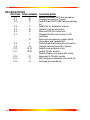
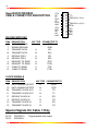
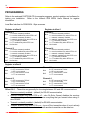
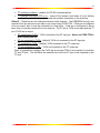
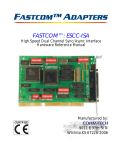
FASTCOM™ ADAPTERS
SuperFASTCOM
Four Channel High-Speed Synchronous Serial Adapter
for PCI Bus
Hardware Reference Manual
Manufactured by:
9011 E 37th St N
Wichita KS 67226-2006
9011 E. 37TH STREET N.
WICHITA, KANSAS 67226-2006
(316) 636-1131
FAX (316) 636-1163
http://www.commtech-fastcom.com/
COPYRIGHT (C) 2001, 2002, 2003, 2004, 2005
All rights reserved, including those to reproduce this document or parts thereof in
any form without permission in writing from Commtech, Inc.
FASTCOM is a trademark of Commtech, Inc.
Microsoft is a registered trademark of Microsoft Corporation.
WINDOWS is a trademark of Microsoft Corporation.
REVISION NOTES
REVISION PAGE NUMBER
2.1
12
2.2
20
2.3
5
2.4
2.5
2.6
2.7
11
19
10
1
13
2.8
2.9
2.10
2.11
1
18
12-13
19-21
2.12
2.13
2.14
21
11
14
CHANGES MADE
Revised Windows 2000 test procedure
Changed warranty to 2 years
Added SuperFASTCOM Cable to packing
list
Added link to installation manual
Updated contact information
Removed RS-530 references
Changed board revision level on CE
certificate
Removed unnecessary register setup
information and repaginated
Added SuperFastcom family information
Changed warranty period to lifetime
Added more programs to list
Added “Errata” section
Modified features to agree with errata
Appended to “Errata” section
Add hardware installation notes 2a & 2b
Add register descriptions
CONTENTS
“CE” CERTIFICATE .............................................................................................................. 1
INTRODUCTION
Description / Block Diagram ............................................................................................ 3
Specifications / Features ................................................................................................. 4
Board Layout ................................................................................................................... 5
Communications Overview .............................................................................................. 6
Comparison to ESCC Family........................................................................................... 8
CABLE
Cable Configuration......................................................................................................... 9
DB25 Connector Description ......................................................................................... 10
INSTALLATION
Hardware Installation..................................................................................................... 11
Software Installation ...................................................................................................... 11
TESTING THE INSTALLATION
Windows 2000 Test Procedure...................................................................................... 11
SOFTWARE UTILITIES...................................................................................................... 12
PROGRAMMING ................................................................................................................ 14
MEMORY MANAGEMENT ................................................................................................. 16
RS-422/485......................................................................................................................... 17
Termination Resistance................................................................................................. 18
PROGRAMMABLE CLOCK GENERATORS ...................................................................... 19
ERRATTA ........................................................................................................................... 20
TECHNICAL SUPPORT ..................................................................................................... 23
APPENDIX A
Infineon 20534 Technical Data Sheet............................................................................ 24
1
EUROPEAN UNION DECLARATION OF CONFORMITY
Information Technology Equipment
The Company COMMTECH, INC. declares under its own and full responsibility that the product
" SuperFastcom - Revision 2.0 "
on which is attached this Certificate is compliant to the "89/336/EEC" Directive, amended by 92/31/EEC and
93/88/EEC.
[ ]
The product identified above complies with the requirements of the above EU Directive by meeting the
following standards:
•
EN 50081-1 (1992) EMC Generic Emission Standard - Part 1, Residential, Commercial and Light Industry
- EN 55022 (1995), CISPR 22 (1993) Limits and Methods of Measurement of Radio Disturbance
Characteristics of Information Technology Equipment, 30 MHz - 1 GHz, Class B Limits
•
EN 50082-1 (1992) EMC Generic Immunity Standard - Part 1, Residential, Commercial and Light Industry
- IEC 801-2 (1984), Method of Evaluating Susceptibility to Electrostatic Discharge, Level 4
- IEC 801-3 (1984), Radiated Electromagnetic field Requirements, Level 3
- IEC 801-4 (1988), Electrical Fast Transient/Burst Requirements, Level 2
Products listed on this declaration are exempt from the requirements of the 73/23/EEC directive due to the input
voltage specification as stated in Article 1 of the directive.
The technical documentation required to demonstrate that this product meets the requirements of the EMC Directive
has been compiled by the signatory below and is available for inspection by the relevant enforcement authorities.
In WICHITA, KS on December 31st of 1995
9011 E. 37th Street North
Wichita, KS 67226-2006
(316) 636-1131
Fax (316) 636-1163
Mr. Glen R. Alvis
Chief Engineer
2
3
INTRODUCTION
The new SuperFASTCOM PCI adapter is a very high-speed, four channel, synchronous serial
communications adapter designed for Windows- and LINUX-based industrial/commercial
systems. Its outstanding features include data rates up to 40 Mbits/s and the ability to buffer
up to 4 Gigabytes of data (Windows 2000) in system memory.
The SuperFASTCOM supports standard synchronous protocols (HDLC, SDLC) and their
variations, as well as standard asynchronous data formats at data rates up to 40 Mbits/s. The
on-board clock generator provides a high-speed clock source for your system and
eliminating the need for an external clock. The board also features high-speed RS-422/RS485 drivers/receivers with on-board line termination.
Programming is simplified with the inclusion of drivers, example programs and comprehensive
documentation supplied on the Fastcom CD. The SuperFASTCOM provides high speed and
high reliability while greatly reducing development time and system complexity.
The SuperFASTCOM family includes:
Form Factor
PCI
PC/104+
CompactPCI
CompactPCI Rear IO
Line Type
RS422/485 OR RS232
RS422/485
RS422/485
RS422/485
Ports
4
1 or 2
4
4
The following diagram illustrates the basic structure of the SuperFASTCOM:
Status
LEDs
Programmable High Speed Clock Source
PCI Bus
2
3
4
Channels
Communication
Processor
Memory
Controller
Bus Control
Logic
1
Termination
Resistance
Clock
Generator
#1
Drivers/
Receivers
Clock
Generator
#2
4
SPECIFICATIONS:
COMMUNICATION CONTROLLER:
INFINEON 20534
OS SUPPORT:
Windows XP, 2000, NT4; Linux
DATA RATE:
All baud rates up to 40 Mbps
DATA BUFFERING:
Up to 4 Gbytes (Windows)
Up to 52 Mbytes per channel (LINUX)
DRIVERS/RECEIVERS:
High Speed RS-422/RS-485
SIGNALS:
TxD, RxD, RTS, CTS, DCD, TT, RT, ST
CONNECTOR CONFIGURATION:
DB-78 to four DB-25 connectors
BUS INTERFACE:
32-bit PCI Ver. 2.1
POWER REQUIREMENTS:
450mA @ +5 (typical)
ENVIRONMENT:
Operating Temperature Range: 0 to 70 C
Humidity:
0 to 90% (non-condensing)
MEAN TIME BETWEEN FAILURES:
24.61 Yrs
CERTIFICATION:
FCC compliant, CE marked
FEATURES:
Four independent channels
Status LEDs for system development/debugging
Two programmable on-board clock generators
“Switchless” design for durability and reliability
Hardware documentation and software included on CD
Made in Wichita, KS U.S.A.
5
SuperFASTCOM
BOARD LAYOUT
TRANSMIT/
RECEIVE
STATUS
LEDs
DB78
CONNECTOR
Commtech, Inc.
Wichta, KS
PACKING LIST:
SuperFASTCOM Card
SuperFASTCOM Cable
FASTCOM CD
If an omission has been made, please call technical support for a replacement.
6
COMMUNICATIONS OVERVIEW
HDLC/SDLC Protocol Modes
- Automatic flag detection and transmission
- Shared opening and closing flag
- Generation of interframe-time fill ’1’s or flags
- Detection of receive line status
- Zero bit insertion and deletion
- CRC generation and checking (CRC-CCITT or CRC-32)
- Transparent CRC option per channel and/or per frame
- Programmable Preamble (8 bit) with selectable repetition rate
- Error detection (abort, long frame, CRC error, short frames)
Bit Synchronous PPP Mode
- Bit-oriented transmission of HDLC frame (flag, data, CRC, flag)
- Zero bit insertion/deletion
- 15 consecutive ’1’ bits aborts sequence
Octet Synchronous PPP Mode
- Octet-oriented transmission of HDLC frame (flag, data, CRC, flag)
- Programmable character map of 32 hard-wired characters (00 H -1F H)
- Four programmable characters for additional mapping
- Insertion/deletion of control-escape character (7D H) for mapped characters
Asynchronous (ASYNC) Protocol Mode
- Selectable character length (5 to 8 bits)
- Even, odd, forced or no parity generation/checking
- 1 or 2 stop bits
- Break detection/generation
- In-band flow control by XON/XOFF
- Immediate character insertion
- Termination character detection for end of block identification
- Time out detection
- Error detection (parity error, framing error)
BISYNC Protocol Mode
- Programmable 6/8-bit SYN pattern (MONOSYNC)
- Programmable 12/16-bit SYN pattern (BISYNC)
- Selectable character length (5 to 8 bits)
- Even, odd, forced or no parity generation/checking
- Generation of interframe-time fill ’1’s or SYN characters
- CRC generation (CRC-16 or CRC-CCITT)
- Transparent CRC option per channel and/or per frame
- Programmable Preamble (8 bit) with selectable repetition rate
- Termination character detection for end of block identification
- Error detection (parity error, framing error)
Extended Transparent Mode
- Fully bit transparent (no framing, no bit manipulation)
- Octet-aligned transmission and reception
Protocol and Mode Independent
- Data bit inversion
7
- Data overflow and under run detection
- Timer
Protocol Support
Address Recognition Modes
- Mode 0 - No address recognition
- Mode 1 - 8-bit (high byte) address recognition
- Non-Auto Mode - 8-bit (low byte) or 16-bit (high and low byte) address recognition
General
On-chip Rx and Tx data buffer (the buffer size is 128 32-bit words each)
Programmable buffer size in transmit direction per channel; buffer allocation in receive
direction on request.
Programmable watermark for receive channels to control transfer of receive data to
host memory.
Two programmable watermarks for each transmit channel, i.e. one controlling data
loading from host memory and one controlling transfer of transmit data to the
corresponding Serial Communication Controller (SCC).
Internal test loop capability.
8
SuperFASTCOM / ESCC FAMILY COMPARISON
Enhancements to the ESCC Serial Core
The SuperFASTCOM adapter contains the core logic of the ESCC2 V3.2A as the heart of the
device. Some enhancements are incorporated in the SuperFASTCOM. These are:
16-Kbyte packet length byte counter
Enhanced address filtering (16-bit maskable)
Enhanced time slot assigner
Support of high data rates (45 Mbit/s for DS3 or 52 Mbit/s for OC1). Protocol support is
limited to HDLC Sub-modes without address recognition.
Simplifications of the ESCC Serial Core
The following features of the ESCC core have been removed:
SDLC Loop mode
Extended transparent mode 0 (this mode provided octet buffered data reception without
usage of FIFOs; the SuperFASTCOM supports octet buffered reception via appropriate
threshold configurations for the SCC receive FIFOs)
9
CONFIGURATION FOR SuperFASTCOM CABLE ASSEMBLY
The cable provided with your SuperFastcom adapter splits each channel from the DB78 to into
four DB 25 male connectors.
SIGNAL
GND
GND
SDSD+
RDRD+
RTSRTS+
CTSCTS+
DCDDCD+
TTTT+
RTRT+
STST+
PRGCLKPRGCLK+
DB25 #
1
7
2
14
3
16
4
19
5
13
10
8
11
24
9
17
12
15
23
20
CHANNEL 1
58
68
70
50
73
53
71
51
74
54
76
57
69
52
72
56
75
55
77
78
DB78 PIN NUMBER
CHANNEL 2 CHANNEL 3
38
9
29
10
13
22
32
2
36
6
17
26
33
3
14
23
18
27
37
7
31
8
12
28
30
1
11
21
16
25
35
5
34
4
15
24
N/A
N/A
N/A
N/A
CHANNEL 4
48
49
62
46
65
42
63
45
66
41
40
60
61
47
64
43
67
44
N/A
N/A
10
SuperFASTCOM DB25
CABLE CONNECTOR DESCRIPTION
CTS+
STTTDCDRTDCD+
GND
CTSRTSRDSDGND
PIN DESCRIPTIONS
PIN#
1
7
2
14
3
16
4
19
5
13
DESCRIPTION
422 TYPE CONNECTED TO
SHIELD/GROUND
GND
SIGNAL/GROUND
GND
TRANSMIT DATA
A
SDTRANSMIT DATA
B
SD+
RECEIVE DATA
A
RDRECEIVE DATA
B
RD+
REQUEST TO SEND
A
RTSREQUEST TO SEND
B
RTS+
CLEAR TO SEND
A
CTSCLEAR TO SEND
B
CTS+
CLOCK SIGNALS
PIN#
8
10
24
11
17
9
15
12
DESCRIPTION
422 TYPE CONNECTED TO
DATA CARRIER DETECT
A
DCD+
DATA CARRIER DETECT
B
DCDTRANSMIT CLOCK OUT
A
TT+
TRANSMIT CLOCK OUT
B
TTRECEIVE CLOCK IN
A
RT+
RECEIVE CLOCK IN
B
RTTRANSMIT CLOCK IN
A
ST+
TRANSMIT CLOCK IN
B
ST-
Special Signals On Cable 1 Only
Pin 20
Pin 23
PROGCLK +
PROGCLK-
Programmable clock output
13
12
11
10
9
8
7
6
5
4
3
2
1
25
24
23
22
21
20
19
18
17
16
15
14
TT+
PROGCLK- (CH1)
PROGCLK+ (CH1)
RTS+
RT+
RD+
ST+
SD+
11
INSTALLATION
Important:
Observe Electrostatic Discharge (ESD) precautions when handling the
SuperFASTCOM board.
1.
Unpack the SuperFASTCOM adapter. Keep the box and static bag for warranty repair
returns.
2.
Select an open PCI slot in your PC.
a.
The SuperFastcom requires that the selected PCI slot be capable of bus mastering.
The card will not function correctly if installed into a non-bus mastering slot.
b.
If possible, install the SuperFastcom into one of the Primary PCI slots. If you are
installing into a Secondary PCI slot (i.e., on the other side of a PCI bridge), make sure
that your motherboard’s PCI bridge is properly installed in your operating system
before proceeding with the installation. If you do not have more than three PCI slots,
then none of the slots are secondary.
3.
After removing the blank bracket from your PC, install the SuperFASTCOM in the PC by
pressing it firmly into the slot. Install the bracket screw to hold it firmly in place.
4.
Re-install the cover on your PC.
5.
Install the SuperFASTCOM cable.
Software Installation
Select the link above to open the Installation Manual. Under SuperFastcom, select your
operating system and follow the instructions. When you are finished, select SuperFastcom
from the list at the end of the SuperFastcom section to return to this manual.
TESTING THE INSTALLATION
To fully test the installation of your SuperFastcom, you will
need to build a "loop back plug". Materials needed are a
DB25 female receptacle (solder cup style) and a few short
pieces of 20 or 24 AWG stranded wire. Jumper the pins
together on the DB25 as illustrated:
WINDOWS 2000 TEST PROCEDURE
1. Place the loop back plug onto the Port 1 connector.
SIGNALS
1
2
3
4
5
6
7
8
9
10
11
12
13
14
15
16
17
18
19
20
21
22
23
24
25
2
3
7
9
10
11
14
16
17
24
SDRDGND
RTDCDTTSD+
RD+
RT+
TT+
12
2.
3.
4.
5.
6.
Open a console/DOS window.
Change directories to where you installed/copied the software.
Execute: setclock 0 4000000
Execute: sfcset 0 hdlcset
Execute: loopback 0 h
The green and red LEDs for port 1 should be blinking/on. Wait a few moments, press a key,
and the errors/number of bytes sent through the loop will be displayed. The numbers will vary
depending on how long you allow the test to run
The rest of the ports can be checked by executing:
sfcset 1 hdlcset
loopback 1 h
sfcset 2 hdlcset
loopback 2 h
sfcset 3 hdlcset
loopback 3 h
SOFTWARE UTILITIES
These programs and their source can be found on the Fastcom CD or downloaded from
our website at http://www.commtech-fastcom.com/. They are meant to be used as
educational tools and programming references when designing your own software.
•
sfcset.exe
•
hdlcset, asyncset, bisyncset
Generic settings files to be used with sfcset.exe
•
getclock.exe
returns programmable clock #1 rate (osc)
•
getclock2.exe
returns programmable clock #2 rate (progclk +/-)
•
setclock.exe
sets the programmable clock #1 (osc)
•
setclock2.exe
sets the programmable clock #2 (prograclk +/-)
•
loopback.exe
user program to effect a loopback on a SuperFastcom channel
•
sfcmfc.exe
o
o
o
o
o
o
Use to change register settings in conjunction with the hdlcset file
Install your loopback plug onto the SuperFastcom.
Run “sfcmfc.exe”.
Select “connect” from the menu.
A dialog will open. Select the port to use (0,1,2,3).
Click on “OK”.
An info box will open; click “OK”.
13
o
o
o
o
o
Type a message: “Hello, world”.
What you type should show up under “Transmit” in the window.
Select “Send” from the menu.
The message will appear in red under “Received”.
To open a different port, either select “File->New” or “Disconnect” from the menu.
•
readlb.exe
user program to read a SuperFastcom special register
•
writelb.exe
user program to read a SuperFastcom special register
•
readreg.exe
user program to read a 20534 register
•
writereg.exe
user program to write to a 20534 register
•
send.exe
user program that opens a file and sends it through port 0
•
flushrx.exe
user program to flush the SuperFASTCOM receiver/buffers
•
flushtx.exe
user program to flush the SuperFASTCOM transmitter/buffers
•
getbufs.exe
user program to get buffering/descriptor parameters for a port
•
setbufs.exe
user program to set buffering/descriptor parameters for a port
•
getclock.exe
user program to get the current clock generator settings
•
getclock2.exe
user program to get the current program clock generator settings
•
read_file_hdlc.exe user program to read hdlc frames from a port and stuff them to a
file
•
sendfile.exe
•
setchecktimeout.exe
user mode function to set the timeout timer in the driver
that checks for frames to be returned or sent
•
setfs6131clock.exe user program that sets the fs6131 clock generator which is only
valid if you have an extended temperature card with fs6131’s on it
•
setrfi.exe
user program to mask/unmask the frame end interrupt indication for
receive descriptors
•
setrirq.exe
user program to set the interrupt rate for receive descriptors
•
settirq.exe
user program to set the interrupt rate for transmit descriptors
•
settfi.exe
user program to mask/unmask the frame end interrupt indication for
transmit descriptors
•
simuln200.exe
user program to generate 26 byte hdlc frames simulating an LN200
•
st_tt.exe
user program to switch the onboard txclk multiplexer between the
TT output and the ST input
•
status.exe
user program to read status from a SuperFastcom port
user program to send a file out a SuperFastcom port
14
PROGRAMMING
Refer to the enclosed FASTCOM CD for example programs, product updates, and software for
testing your installation. Refer to the Infineon PEB 20534 User's Manual for register
information.
Local Bus Interface for PEB 20534 - Byte accesses
Register at offset 0
Register at offset 1
Channel 1
Channel 3
Bit 0
Bit 1
Bit 2
Bit 3
1 = receive constantly enabled
0 = receive enabled only when RTS is off
1 = transmit constantly enabled
0 = transmit enabled only when RTS is on
1 = TT constantly enabled
0 = TT enabled only when RTS is on
No function
Channel 2
Bit 4
Bit 5
Bit 6
Bit 7
1 = receive constantly enabled
0 = receive enabled only when RTS is off
1 = transmit constantly enabled
0 = transmit enabled only when RTS is on
1 = TT constantly enabled
0 = TT enabled only when RTS is on
No function
Bit 0
Bit 1
Bit 2
Bit 3
1 = receive constantly enabled
0 = receive enabled only when RTS is off
1 = transmit constantly enabled
0 = transmit enabled only when RTS is on
1 = TT constantly enabled
0 = TT enabled only when RTS is on
No function
Channel 4
Bit 4
Bit 5
Bit 6
Bit 7
1 = receive constantly enabled
0 = receive enabled only when RTS is off
1 = transmit constantly enabled
0 = transmit enabled only when RTS is on
1 = TT constantly enabled
0 = TT enabled only when RTS is on
No function
Register at offset 2
Channel 1
Bit 0
Bit 1
0 = ST connected to TXCLK
1 = ST not connected
0 = TT connected to TXCLK
1 = TT not connected
Channel 2
Bit 2
Bit 3
0 = ST connected to TXCLK
1 = ST not connected
0 = TT connected to TXCLK
1 = TT not connected
Channel 3
Bit 4
Bit 5
0 = ST connected to TXCLK
1 = ST not connected
0 = TT connected to TXCLK
1 = TT not connected
Channel 4
Bit 6
Bit 7
0 = ST connected to TXCLK
1 = ST not connected
0 = TT connected to TXCLK
1 = TT not connected
Offset 0 & 1 – These bits are generally for choosing between 422 and 485 communications.
Receive constantly enabled – (default) for RS-422 communication
Receive enabled only when RTS is off – also Rx Echo Cancel; disables the receiver
when transmitting so that you do not receive everything that you transmit when using 2wire RS-485.
Transmit constantly enabled – (default) for RS-422 communication
Transmit enabled only when RTS is on – turns off the transmitter when it is not actively
sending data so that it does not contend with another transmitter on the data bus
15
TT constantly enabled – (default) for RS-422 communications
TT enabled only when RTS is on – turns off the transmit clock when it is not actively
sending data so that it does not contend with another transmitter on the clock bus
Offset 2 – These bits are for setting the transmit clock direction. The PEB20534 has only one
transmit clock pin that can be an input or an output using CCR0:TOE. If that pin is configured
to be an output, then it must be connected to a line driver. If that pin is configured to be an
input, then it must be connected to a line receiver. The ST pin is TxClk as an input and the TT
pin is TxClk as an output.
ST connected to TxClk – TxClk connected to the ST input pin. Never set CCR0:TOE=1
when setting this bit!
ST not connected to TxClk – (default) TxClk not connected to the ST input pin
TT connected to TxClk – (default) TxClk connected to the TT output pin
TT not connected to TxClk – TxClk not connected to the TT output pin.
Note: It is possible to configure the TxClk pin as an input TOE=0, and connect it to both the
TT and ST pins. This will allow the external clock from the ST pins to be outputted on the
TT pins.
16
MEMORY MANAGEMENT
High-speed communications requires that large amounts of transmitted/received data be
buffered so as to prevent data loss and maintain data throughput. The SuperFASTCOM is
designed to utilize system memory directly, bypassing the system processor.
The
SuperFASTCOM accesses system memory through high-speed PCI Bus Mastering, using its
on-board bus master controller and supplied software. This procedure for direct memory
access (DMA) is by far the fastest, most efficient method of handling the large amounts of data
that high-speed communications generates.
Data is transferred to and from the
SuperFASTCOM adapter at data bus speed. Buffering a high-speed data stream is critical in
order to maintain data integrity and reliability, to avoid data loss, and to prevent data overrun.
The SuperFASTCOM does all this with minimal system processor involvement, therefore there
is no reduction in processor performance due to data communication overhead.
How it works - The user designates in his program how much system memory will be allocated
to communications: the more memory in your system, the more you can allocate to the
communication process. As data is received, the on-board communication processor fills a
small local buffer. When this is full, the bus master controller on the SuperFASTCOM transfers
this data directly to system memory. The local buffer is reset and the process begins again.
Transmitting data works in reverse; data from system memory is directly transferred to the
local buffer on the SuperFASTCOM. When the local buffer is empty, new data from memory is
directly transferred in. All of this occurs without slowing or interfering with the system
processor.
The high speed PCI Bus Mastering procedure for direct memory access provides the fastest,
most efficient method of data transfer. It also improves efficiency and reduces the cost of the
SuperFASTCOM board by eliminating the need for on-board memory or a processor.
17
RS-422 / RS-485
Most engineers have worked with RS-232 devices at least once in their career. If you have
never worked with RS-422 or RS-485 devices, you will be pleased to know that working with
the SuperFASTCOM is not much different from working with an RS-232 device.
The RS-422 standard was developed to correct some of the deficiencies of RS-232. In
commercial and industrial applications, RS-232 has some significant problems. First, the cable
length between RS-232 devices must be short (usually less than 50 feet at 9600 Baud).
Second, many RS-232 errors are the result of cables picking up normal industrial electrical
noises such as fluorescent lights, motors, transformers, and other EMF sources. Third, RS232 data rates are functionally limited to 19.2K Baud. On the other hand, the newer RS-422
standard makes cable lengths up to 5000 feet possible and is highly immune to most industrial
noises. Data rates are also improved -- the SuperFASTCOM features data rates up to 40
Mega Baud. These improvements were made possible by differentially driving and receiving
the data as opposed to the single ended method employed by the RS-232 standard. With the
RS-422 standard, the transmit signal (TX in RS-232) is a differential signal consisting of SD+
and SD-; the receive signal (RX in RS-232) consists of RD+ and RD-.
Another draw back of RS-232 is that more than two devices cannot share a single cable. This
is also true of RS-422, and that's why the RS-485 standard was developed. RS-485 offers all
of the benefits of RS-422 and also allows multiple units (up to 32) to share the same twisted
pair. RS-485 is often referred to as a "multi-drop" or "two-wire, half duplex" network because
the drivers (transmitters) and receivers share the same two lines. In fact, up to 32 stations can
share the same "twisted pair". In order for an RS-485 system to work, only one driver
(transmitter) can occupy the network at a time. This means that each station on the network
must control the enabling/disabling of their drivers in order to avoid network conflicts. If two
drivers engage the network at the same time, data from both will be corrupted. In RS-485
mode, the receivers are always enabled.
For a more detailed description of RS-422 and RS-485, we recommend the following
references:
LINEAR AND INTERFACE CIRCUITS APPLICATIONS, Volume 2: Line Circuits,
Display Drivers. By D.E. Pippenger and E. J. Tobaben. Published 1985 by Texas
Instruments. ISBN-0-89512-185-9
Note: This book may be difficult to find in a bookstore. The best place to get it is
directly from Texas Instruments or from one their component dealers. Publication #
SLYA002.
"Driver/Receiver Family Extends Data-Link Performance", ELECTRONIC PRODUCTS,
January 15, 1985. By Dale Pippenger and Joe Miller
18
TERMINATION RESISTANCE
In both the RS-422 and the RS-485 mode, the receiver end of the cable between two stations
must be terminated with a resistor equal to the characteristic impedance of the wire. This is to
prevent signal reflections in the wire and to improve noise rejection. However, you do not
need to add a terminator resistor to your cables when you use the SuperFastcom. The
termination resistance is built in. We have installed a terminator resistor for each receiver:
between each RD+ and RD- and between CTS+ and CTS- for each channel.
If you are using the SuperFastcom in a multi-drop network, the termination resistor should be
removed from all units except the first and last (see the RS-485 illustration below). Call for
technical support if you need to modify the resistor. You may also order the SuperFastcom
without the termination resistor installed (it is easier to add the resistor than to remove it).
Observe the resistors in the following drawings and remember that they are built into the
SuperFastcom:
19
PROGRAMMABLE CLOCK GENERATORS
The SuperFastcom features two Programmable Clock Generators. Each is a Cypress
ICD2053B chip, which offers a fully user-programmable phase-locked loop clock pulse
generator in a single 8-pin package. The output of the generator may be changed "on the fly"
to any desired frequency value. The ability to dynamically change the output frequency adds a
whole new degree of freedom for the designer.
Why have two clock generators?
The first clock generator (the OSC clock generator) provides the clock pulse to the PEB20534
communications processor chip. Its maximum frequency is 33MHz and is programmable via
the GPP register (bits 8 and 9). The second clock generator (the PROGCLK clock generator)
directly drives the PROGCLK+ and PROGCLK- output signals (PIN 20 and 23 on Cable #1).
The PROGCLK has a maximum frequency of 40MHz and is programmable via the GPP
register (bits 10 and 11). The PROGCLK is designed to provide a system wide high-speed
clock pulse.
For additional information on the Cypress ICD2053B, please review the data sheet.
An important fact about the clock generator
There is only one clock input line on the PEB 20534 communications chip and it is connected
to the OSC clock generator on the SuperFastcom board. The OSC clock generator can be
programmed from any channel (SFC, SFC1, SFC2, SFC3) but you are programming the same
clock generator (the OSC clock generator) in each case. Just keep in mind that the baud rate
generators are independent for each channel, but all four baud rate generators are fed from
one clock source (the OSC clock generator). If you change the OSC clock generator rate you
will change the input to the baud rate generators for all channels.
If you have multiple baud rates that must be generated on multiple channels, you should select an OSC
clock rate from which all of the required baud rates can be derived. Changing the OSC clock generator
output will affect the baud rates of all channels!!!!
20
ERRATA
The errata listed below are known issues with the either Superfastcom board or the PEB20534
controller itself. For more information regarding any of these issues, please contact
Commtech technical support.
•
Serial Bus Configuration Timing Modes
The SuperFastcom was not designed to make use of Serial Bus Configuration timing
modes 1 and 2. Do not attempt to configure CCR0:SC(2..0) to use these modes as
they will not work correctly.
•
Maximum Value of Baudrate Generator
The maximum value ’BRM’ in register BRR must not exceed M = 14 (the specified
maximum value is M = 15). This limits the baud rate generator unit to frequency division
factors in the range k = 1... 1,048,576, instead of k = 1... 2,097,152.
•
DPLL Algorithm for FM0, FM1 and Manchester Encoding
Recovering the clock from an FM0-, FM1- or Manchester-encoded receive data stream
using the DPLL circuitry is not working. The DPLL-asynchronous interrupt (PLLA)
occurs continuously.
•
HDLC Mode: False Receive Status Byte
The receive status byte RSTA belonging to an already received frame is overwritten by
0x00 if the following two conditions are met:
1. The interframe timefill number of ’1’ bits between the closing flag and the opening
flag of the next frame is in the range of [1 - 5].
2. The receive CRC checking mode is selected to transfer the receive CRC into the
receive FIFO (CCR2:RCRC = ’1’).
In all cases meeting the first condition, the number of ‘1’ bits is treated as an invalid
HDLC frame. This frame is prevented from being reported or forwarded to the receive
FIFO because of its invalid length. However the serial receive logic calculates a receive
status byte RSTA = 0x00 (invalid frame).
If the receive CRC is selected to be transferred to the receive FIFO (second condition),
the receive status value of the previous valid frame is not yet transferred when
calculating the invalid receive status byte. Thus the original receive status value is
overwritten by 0x00 marking the previous frame as ’invalid’.
Workaround: The error cannot occur if bit CCR2:RCRC is set to ’0’, i.e. receive CRC is
not transferred to the receive FIFO. Otherwise (if CCR2:RCRC = ’1’) reception of less
than 6 consecutive ’1’ bits as interframe timefill must be avoided. This can be achieved
by the transmitter either selecting interframe timefill flag sequences or preamble
transmission.
•
HDLC Mode: Transmission with Shared Flags
If the shared flag option is enabled in HDLC mode via bit CCR1:SFLAG, the first byte of
a frame might be replaced by a ’7E’ flag or ’FF’ octet on the transmit line, depending on
the interframe time fill selection (bit CCR2:ITF). This leads to a damaged transmit
frame.
21
Workaround: It is recommended to disable shared flag transmission by setting bit
CCR1:SFLAG = ’0’.
Note: Reception of frames with shared flags is always possible and neither
affected by this erratum nor by setting of bit CCR1:SFLAG. Thus networking with
other HDLC equipment supporting shared flags is not restricted.
•
Asynchronous PPP Mode: Reception
In asynchronous PPP mode the SCC receiver expects a back-to-back stream of
ASYNC characters. Once synchronized on the first ASYNC character the receiver
expects further octets back-to-back in a fixed scheme determined by the (8, N, 1)
character format. The receiver does not synchronize again on subsequent ASYNC
characters.
Workaround: Do not attempt to configure ASYNC PPP mode, to realize asynchronous
PPP mode it is recommended to configure the SCC in ASYNC mode, implementing
CRC calculation and character mapping in software. Examples for fast CRC calculation
and the character mapping specification are given in RFC 1662 (July 1994) document.
•
Extended Transparent Mode: Minimum Frame Length
If the frame length in extended transparent mode is programmed to one, an XDU
interrupt is generated with all its consequences (transmit SCC stops).
Workaround: Frame lengths of 2 or more bytes should be used instead. If a 1-byte
frame shall be sent, an idle character should be attached to it.
•
HDLC Automode: Full-duplex Operation
In HDLC Automode the transmission of an I-frame might be spoiled by simultaneous
reception of a frame, sometimes resulting in endless repetition of a byte or in failure of
the responding S-frame. Then this channel does not respond autonomously to further
reception events.
Workaround: None. Do not use full-duplex Automode.
•
Command Execution (CEC) Status Bit Error With External Clocking
In general the PEB20534 supports external clock gapping in any clock mode in which
the internal transmit or receive clock is supplied via the dedicated RxClk and/or TxClk
pins. If one of the clocks is externally gapped, the respective receive or transmit block
remains in its current static condition until the clock signal is active again. Any
command bit in register CMDR (e.g. ’XRES’ and ’RRES’) effects either the transmit or
receive logic and command execution only depends on this block and its clock supply
respectively. Nevertheless all commands are forwarded to both transmit and receive
block and command execution must be reported internally by both blocks to reset status
bit STAR:CEC. Another command is only accepted if ’CEC’ bit is cleared.
Example: The SCC is configured in clock mode 0a, a clock signal is provided at pin
TxClk but pin RxClk is supplied with a constant value (no clock signal or gapped). A
transmitter reset command applied by write access to register CMDR will be executed
by the transmit block, but status bit ’CEC’ remains active afterwards, because the
receive block cannot report command execution without clock supply. Any further
command will be ignored while ’CEC’ bit is active.
Workaround: Transmit and receive blocks must be supplied with clock signals in
general. Because reset of the command execution (CEC) status bit might be delayed
22
due to one of the clocks temporarily gapped, ’CEC’ status bit must be checked for ’0’
before writing a command bit.
•
Carrier Auto-detect in HDLC Mode
The carrier detect (CD) input pin is supposed to enable and disable reception in clock
modes 0, 2, 3, 6 and 7. In HDLC/PPP mode this function is not working properly and
thus should not be enabled with bit CCR1:CAS.
•
Receiver in Extended Transparent Mode Does Not Initialize
When attempting to use Extended Transparent Mode (raw bits), it appears as though
the receiver does not activate. It unclear whether this is a bug in the PEB20534 or
whether it was done by design, but the port that will be receiving in Ext. Trans. Mode
must be initialized in clock mode 1 with a clock present on the RT pins. It can then be
switched to any other clock mode and will operate correctly.
Workaround: If your configuration already uses an external receive clock, simply
initialize the card in clock mode 1 (CCR0:CM2..CM0 = ‘001’) with a clock present on the
RT pins and then change to whatever clock mode you wish to use. If you do not have
an external clock, you can utilize the PROGCLK output pins that are located on the
DB25 connector for port 1 at pins 20 and 23. Jumper the PROGCLK pins to the RT
pins of your receiving port and initialize the card in clock mode 1.
23
TECHNICAL SUPPORT
All products manufactured by Commtech are warranted against defective materials and
workmanship for the lifetime of the product. This warranty is available only to the original
purchaser. Any product found to be defective will, at the option of Commtech, be repaired or
replaced with no charge for labor or parts not excluded by the warranty. This warranty does
not apply to any products that have been subjected to misuse, abuse, or accident or as a result
of service or modification by anyone other than Commtech. In no case shall Commtech
liability exceed the original product purchase price.
If any Commtech product is damaged such that it cannot be repaired, you can return it to
Commtech for replacement under our Non-Repairable Replacement policy, regardless of the
cause of damage. Commtech will replace the unit at 60% of the then-current list price.
Commtech provides extensive technical support and application suggestions. Most of the
problems that occur with the SuperFASTCOM can be corrected by double-checking the switch
positions, your cables and your program. We recommend that you build the loop back plug
that is described in the Programming section of this manual. With that plug, you can quickly
isolate the problem to the board, cables, or software.
If you still have unresolved questions, use the following procedure to get technical support:
1.
Call our Technical Support Staff at (316) 636-1131. They are on duty from 9:00 AM to
5:00 PM Central Time.
If you purchased your board from Kontron America, please call their 7-24 technical
support line at 1-800-480-0044.
2.
Ask for technical support for the SuperFASTCOM. Be ready to describe the problem,
your computer system, your application, and your software.
3.
If necessary, our staff will give you an RMA number (Return Material Authorization). Use
this number on the mailing label and in all references to your board. Put the board back
in its static bag and in its box. Ship the board back to us as directed.
4.
If you prefer, you may FAX a description of the problem to us at (316) 636-1163, or we
can be reached on the Internet at “http://www.commtech-fastcom.com” or by email at
"[email protected]".
Kontron America can be reached by telephone at (800) 480-0044 or on the web at
“http://www.kontron.com/support/index.cfm”.
24
APPENDIX A
INFINEON 20534
TECHNICAL DATA