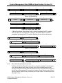
1
System Management Bus (SMBus) Specification Version 3.0 20 Dec 2014 www.powerSIG.org © 2014 System Management Interface Forum, Inc. – All Rights Reserved Filename: Last Saved: SMBus 3_0_20141220.docx 20 December 2014 19:59 System Management Bus (SMBus) Specification Version 3.0 This specification is provided “as is” with no warranties whatsoever, whether express, implied or statutory, including but not limited to any warranty of merchantability, non-infringement or fitness for any particular purpose, or any warranty otherwise arising out of any proposal, specification or sample. In no event will any specification co-owner be liable to any other party for any loss of profits, loss of use, incidental, consequential, indirect or special damages arising out of this specification, whether or not such party had advance notice of the possibility of such damages. Further, no warranty or representation is made or implied relative to freedom from infringement of any third party patents when practicing the specification. Other product and corporate names may be trademarks of other companies and are used only for explanation and to the owner’s benefit, without intent to infringe. Revision No. Date Notes Editor 1.0 2/15/95 General Release Unknown 1.1 12/11/98 Version 1.1 Release Unknown 2.0 8/3/00 Version 2.0 Release Unknown 3.0 20 Dec 2014 Version 3.0 Release Questions and comments regarding this specification may be forwarded to: [email protected] Robert V. White Embedded Power Labs For additional information on Smart Battery System Specifications, visit the SBS Implementer’s Forum (SBS-IF) at: www.sbs-forum.org © 2014 System Management Interface Forum, Inc. All Rights Reserved 2 of 85 System Management Bus (SMBus) Specification Version 3.0 Table of Contents 1. Introduction ............................................................................................................................................. 8 1.1 Overview .................................................................................................................................... 8 1.2 Audience .................................................................................................................................... 8 1.3 Scope......................................................................................................................................... 8 1.4 Organization of this document ................................................................................................... 8 2. Related Documents And Reference Information .................................................................................... 9 2.1 Scope......................................................................................................................................... 9 2.2 Applicable Documents ............................................................................................................... 9 2.3 Reference Documents ............................................................................................................... 9 2.4 Definitions Of Terms ................................................................................................................ 10 2.5 Conventions ............................................................................................................................. 11 2.5.1 Numeric formats ...................................................................................................... 11 2.5.2 SMBus addresses ................................................................................................... 12 2.5.3 Transaction protocol diagrams ................................................................................ 12 3. General Characteristics ........................................................................................................................ 14 4. Layer 1 – The Physical Layer ............................................................................................................... 15 4.1 Electrical Characteristics Of SMBus Devices – Two Discrete Worlds .................................... 15 4.2 SMBus Common AC specifications ......................................................................................... 16 4.2.1 General timing conditions ........................................................................................ 21 4.2.2 Device timeout definitions and conditions ............................................................... 21 4.2.3 Master device clock extension definitions and conditions....................................... 21 4.2.4 Slave device clock extension .................................................................................. 22 4.2.5 SMBDAT low timeout .............................................................................................. 22 4.3 DC Specifications .................................................................................................................... 22 4.3.1 Supply voltage requirements ................................................................................... 23 4.3.2 SMBus branch circuit model ................................................................................... 23 4.3.3 Low Power DC parameters........................................................................................ 24 4.3.4 High Power DC specifications ................................................................................. 25 4.3.5 Additional common Low and High Power specifications......................................... 27 5. Layer 2 – The Data Link Layer ............................................................................................................. 28 5.1 Bit Transfers ............................................................................................................................ 28 5.1.1 Data validity ............................................................................................................. 28 5.1.2 START and STOP conditions ................................................................................. 28 5.1.3 Bus idle condition .................................................................................................... 29 5.2 Data Transfers On SMBus ...................................................................................................... 29 5.3 Clock Generation And Arbitration ............................................................................................ 30 5.3.1 Synchronization ....................................................................................................... 30 5.3.2 Arbitration ................................................................................................................ 31 5.3.3 Clock low extending ................................................................................................ 32 5.4 Data Transfer Formats ............................................................................................................ 34 6. Layer 3 – Network layer ........................................................................................................................ 34 6.1 Usage Model............................................................................................................................ 34 6.1.1 Master devices ........................................................................................................ 34 6.1.2 Slave devices .......................................................................................................... 35 6.1.3 Host ......................................................................................................................... 35 6.2 Device Identification – Slave Address ..................................................................................... 35 © 2014 System Management Interface Forum, Inc. All Rights Reserved 3 of 85 System Management Bus (SMBus) Specification Version 3.0 6.2.1 Uniqueness required ............................................................................................... 35 6.2.2 SMBus address types ............................................................................................. 35 6.3 Using A Device ........................................................................................................................ 37 6.4 Packet Error Checking............................................................................................................. 37 6.4.1 Packet error checking implementation .................................................................... 37 6.5 Bus Protocols........................................................................................................................... 39 6.5.1 Quick Command...................................................................................................... 39 6.5.2 Send Byte ................................................................................................................ 39 6.5.3 Receive Byte ........................................................................................................... 40 6.5.4 Write Byte/Word ...................................................................................................... 40 6.5.5 Read Byte/Word ...................................................................................................... 41 6.5.6 Process Call ............................................................................................................ 42 6.5.7 Block Write/Read..................................................................................................... 42 6.5.8 Block Write-Block Read Process Call ..................................................................... 43 6.5.9 SMBus Host Notify protocol .................................................................................... 44 6.5.10 Write 32 protocol ..................................................................................................... 45 6.5.11 Read 32 protocol ..................................................................................................... 46 6.5.12 Write 64 protocol ..................................................................................................... 46 6.5.13 Read 64 protocol ..................................................................................................... 47 6.6 SMBus Address Resolution Protocol ...................................................................................... 48 6.6.1 Unique Device Identifier (UDID) .............................................................................. 49 6.6.2 Power-on reset ........................................................................................................ 53 6.6.3 ARP commands ...................................................................................................... 53 Appendix A. Optional SMBus signals ......................................................................................................... 72 A.1 SMBSUS#................................................................................................................................ 72 A.2 SMBALERT# ........................................................................................................................... 73 Appendix B. Differences between SMBus and I2C ................................................................................. 75 B.1 VDD And Threshold Voltage Differences .................................................................................. 75 B.2 Minimum Bus Speed And Maximum Clock Stretching ............................................................ 75 B.3 Address Acknowledge ............................................................................................................. 75 B.4 SMBus Protocols ..................................................................................................................... 76 B.5 REPEATED START Condition ................................................................................................ 76 B.6 SMBus Low Power Version ..................................................................................................... 76 B.7 Tables Of Differences .............................................................................................................. 76 Appendix C. SMBus Device Address Assignments .................................................................................... 81 Appendix D. Changes This Revision .......................................................................................................... 83 D.1 Maximum Bus Frequency ........................................................................................................ 83 D.2 Electrical Drive Levels ............................................................................................................. 83 D.3 Data Hold Time ........................................................................................................................ 83 D.4 TSPIKE In Place Of VNOISE .......................................................................................................... 85 D.5 Zone Read And Write Protocols .............................................................................................. 85 D.6 255 Bytes in Process Call........................................................................................................ 85 D.7 32 And 64 Bit Protocols ........................................................................................................... 85 D.8 Reformatting Of Text, Figures, And Tables ............................................................................. 85 © 2014 System Management Interface Forum, Inc. All Rights Reserved 4 of 85 System Management Bus (SMBus) Specification Version 3.0 Table of Tables Table 1. Transaction protocol diagram symbols and elements .................................................................. 12 Table 2. SMBus AC specifications .............................................................................................................. 18 Table 3. Low Power SMBus DC specification............................................................................................. 24 Table 4. High Power SMBus DC specification ............................................................................................ 26 Table 5: UDID bit fields descriptions ........................................................................................................... 49 Table 6: 8-bit device capabilities field descriptions ..................................................................................... 50 Table 7: Version/Revision bit fields description .......................................................................................... 50 Table 8: Interface field bit fields description ................................................................................................ 51 Table 9. Internal state of ARP-capable devices on Power-On Reset ......................................................... 53 Table 10. ARP command number scheme ................................................................................................. 54 Table 11. SMBus device characterizations ................................................................................................. 54 Table 12. Device decodes of AV and AR flags ........................................................................................... 66 Table 13. SMBus Suspend parameters ...................................................................................................... 72 Table 14. Selected parameter differences between Standard-Mode I²C and 100 kHz Class SMBus ....... 76 Table 15. DC parameter differences between Fast-mode I²C and 400 kHz Class SMBus ................. 77 Table 16. DC parameter differences between Fast-mode Plus I²C and 1 MHz Class SMBus ........... 78 Table 17. Reserved and pre-assigned SMBus addresses ......................................................................... 81 Table of Figures Figure 1: Generic transaction diagram........................................................................................................ 14 Figure 2: SMBus Topology.......................................................................................................................... 15 Figure 3: SMBus pull-up circuitry ................................................................................................................ 15 Figure 4: Example input and output stages of SMBus devices .................................................................. 16 Figure 5. SMBus timing measurements ...................................................................................................... 18 Figure 6. Timeout intervals.......................................................................................................................... 21 Figure 7: Clock extension measurement intervals ...................................................................................... 22 Figure 8: SMBus branch with multiple devices attached ......................................................................... 23 Figure 9: SMBus circuit model .................................................................................................................. 24 Figure 10: Data validity ............................................................................................................................... 28 Figure 11: START and STOP conditions .................................................................................................... 28 Figure 12: SMBus byte format .................................................................................................................... 29 Figure 13: ACK signaling of SMBus .......................................................................................................... 29 Figure 14. NACK signaling on SMBus ........................................................................................................ 30 Figure 15: SMBus clock synchronization .................................................................................................... 31 Figure 16: SMBus arbitration .................................................................................................................... 32 Figure 17: Periodic clock stretching by a slave SMBus device .............................................................. 33 Figure 18: Random clock stretching ......................................................................................................... 34 Figure 19: Data transfer over SMBus ...................................................................................................... 34 Figure 20: Quick Command protocol ....................................................................................................... 39 Figure 21: Send Byte protocol .................................................................................................................. 40 Figure 22: Send Byte protocol with PEC..................................................................................................... 40 Figure 23: Receive Byte protocol ............................................................................................................. 40 © 2014 System Management Interface Forum, Inc. All Rights Reserved 5 of 85 System Management Bus (SMBus) Specification Version 3.0 Figure 24: Receive Byte protocol with PEC............................................................................................. 40 Figure 25: Write Byte protocol .................................................................................................................. 40 Figure 26: Write Word protocol ................................................................................................................. 40 Figure 27: Write Byte protocol with PEC ................................................................................................. 41 Figure 28: Write Word protocol with PEC ................................................................................................ 41 Figure 29: Read Byte protocol .................................................................................................................. 41 Figure 30: Read Byte protocol with PEC ................................................................................................. 41 Figure 31: Read Word protocol ................................................................................................................ 41 Figure 32: Read Word protocol with PEC ................................................................................................ 42 Figure 33: Process Call ............................................................................................................................. 42 Figure 34: Process Call with PEC.......................................................................................................... 42 Figure 35: Block Write ............................................................................................................................... 43 Figure 36: Block Write with PEC ............................................................................................................ 43 Figure 37: Block Read ............................................................................................................................... 43 Figure 38: Block Read with PEC .............................................................................................................. 43 Figure 39: Block Write - Block Read Process Call .................................................................................. 44 Figure 40: Block Write - Block Read Process Call with PEC ................................................................. 44 Figure 41: 7-bit Addressable Device to Host Communication ............................................................... 45 Figure 42: Write 32 Protocol ....................................................................................................................... 45 Figure 43: Write 32 Protocol With PEC....................................................................................................... 45 Figure 44: Read 32 Protocol ....................................................................................................................... 46 Figure 45: Read 32 Protocol With PEC ...................................................................................................... 46 Figure 46: Write 64 Protocol ....................................................................................................................... 47 Figure 47: Write 64 Protocol With PEC....................................................................................................... 47 Figure 48: Read 64 Protocol ....................................................................................................................... 48 Figure 49: Read 64 Protocol With PEC ...................................................................................................... 48 Figure 50: UDID ......................................................................................................................................... 49 Figure 51: 8-bit device capabilities field ................................................................................................... 50 Figure 52: Version/Revision field ................................................................................................................ 50 Figure 53: Interface field ........................................................................................................................... 51 Figure 54: Prepare to ARP command ......................................................................................................... 55 Figure 55: Reset device command ............................................................................................................. 56 Figure 56: Get UDID (general) command ................................................................................................... 56 Figure 57: Assign address command ......................................................................................................... 58 Figure 58: Get UDID (directed) command ............................................................................................... 59 Figure 59: Reset device ARP (directed) command ................................................................................ 59 Figure 60: Notify ARP master command ................................................................................................. 60 Figure 61: ARP master behavior flow diagram ........................................................................................... 63 Figure 62: ARP-capable device behavior ................................................................................................... 67 Figure 63: SMBus during suspend.............................................................................................................. 72 Figure 64: Using SMBus to Resume from Suspend ............................................................................... 73 Figure 65: A 7-bit-Addressable Device responds to an ARA ................................................................. 74 Figure 66: A 7-bit-Addressable Device responds to an ARA with PEC ................................................ 74 Figure 67. Showing SMBDAT Remaining Stable Until SMBCLK Is Low .................................................... 83 © 2014 System Management Interface Forum, Inc. All Rights Reserved 6 of 85 System Management Bus (SMBus) Specification Version 3.0 Figure 68. I²C Style Data Hold Time Specification And Implementation .................................................... 84 © 2014 System Management Interface Forum, Inc. All Rights Reserved 7 of 85 System Management Bus (SMBus) Specification Version 3.0 1. Introduction 1.1 Overview The System Management Bus (SMBus) is a two-wire interface through which various system component chips and devices can communicate with each other and with the rest of the system. It is based on the principles of operation of the I2C bus. Appendix B provides a description of some of the ways the SMBus characteristics are different from those of the I²C bus. SMBus provides a control bus for system and power management related tasks. A system may use SMBus to pass messages to and from devices instead of using individual control lines. Removing the individual control lines reduces pin count. Accepting messages ensures future expandability. With System Management Bus, a device can provide manufacturer information, tell the system what its model/part number is, save its state for a suspend event, report different types of errors, accept control parameters, and return its status. 1.2 Audience The target audience for this document includes but is not limited to: • System designers implementing the System Management Bus Specification in their systems • Digital IC design engineers designing chips to connect to the System Management Bus • Software engineers writing support code for System Management Bus chips 1.3 Scope This document describes the electrical characteristics, network control conventions and communications protocols used by SMBus devices. These can be thought of as existing at the first three layers of the seven-layer OSI network model, that is, the physical, data link and network layers. Functions normally implemented at higher layers of the OSI model are beyond the scope of this document. The original purpose of the SMBus was to define the communication link between an intelligent battery, a charger for the battery and a microcontroller that communicates with the rest of the system. However, SMBus can also be used to connect a wide variety of devices including power-related devices, system sensors, inventory EEPROMs, communications devices, and more. This version of the specification is a superset of previous versions, 1.0, 1.1, and 2.0. The intent is that all devices compliant with these previous versions are compliant with this version. Those features new to SMBus with this version of the specification are optional and are appropriate to the new environments enabled by those features. However, if implemented, these new features must be implemented in a manner compliant with this specification. 1.4 Organization of this document This document is organized to first give the reader an overview of the SMBus and then to delve deeper into its actual workings. The major technical discussion appears in three sections that treat the various aspects of the SMBus as they would appear in © 2014 System Management Interface Forum, Inc. All Rights Reserved 8 of 85 System Management Bus (SMBus) Specification Version 3.0 the first three layers of the OSI reference network model: the physical layer, the data link layer and the network layer. The section on the physical layer sets out SMBus electrical characteristics. The section on the data link layer specifies bit transfers, byte data transfers, arbitration, and clock signals. The section on the link layer deals with the general usage model, the concept of addresses in SMBus, the Address Resolution Protocol and the bus data transfer protocol. All aspects of the SMBus proper may be described within the scope of the first three OSI layers. The SMBus is a multiple attachment bus with no routing capability. Most communication occurs between and involves only two nodes, a master and a slave. Exceptions to this rule occur during and apply to devices that implement the Address Resolution Protocol as well as the Alert Response Address. Appendixes at the end of this document contain additional information and guides to implementation that the reader may find useful. 2. Related Documents And Reference Information 2.1 Scope If the requirements of this specification and any of the reference documents are in conflict, this specification shall have precedence unless otherwise stated. Referenced documents apply only to the extent that they are referenced. The latest version and all amendments of the referenced documents at the time the device is released to manufacturing apply. 2.2 Applicable Documents Applicable documents include information that is, by extension, part of this specification. None in this revision. 2.3 Reference Documents Reference documents have background or supplementary information to this specification. They do not include requirements or specifications that are considered part of this document. [R01] The I²C-bus Specification And User Manual, NXP Semiconductors, Revision 6, 4 April 2014 [R02] Advanced Configuration and Power Interface Specification, Hewlett-Packard Corporation, Intel Corporation, Microsoft Corporation, Phoenix Technologies Ltd., and Toshiba Corporation, Revision 5.0a, 13 November 2013 [R03] Conventional PCI, PCI Special Interest Group, Revision 3.0 [R04] PCI Express, PCI Special Interest Group, Revision 3.0 [R05] SMBus Control Method Interface Specification, System Management Interface Forum, Version 1.0, 10 December 1999 [R06] PMBus™ Power System Management Protocol Specification Part I – General Requirements, Transport And Electrical Interface, System Management Interface Forum, Revision 1.3, March 2014 © 2014 System Management Interface Forum, Inc. All Rights Reserved 9 of 85 System Management Bus (SMBus) Specification Version 3.0 2.4 Definitions Of Terms The following terms are defined with respect to this specification and may have other meanings in other contexts. Some of these terms are used throughout the specification while others have meaning only within limited portions. Term Definition Address Resolution Protocol A protocol by which SMBus devices with assignable addresses on the bus are enumerated and assigned non-conflicting slave addresses. Address Resolved flag (AR) A flag bit or state internal to a device that indicates whether or not the device’s slave address has been resolved by the ARP Master. Address Valid flag (AV) A flag bit or state internal to a device that indicates whether or not the device’s slave address is valid. This bit must be non-volatile for devices that support the Persistent Slave Address. Alert Response Address (ARA) A broadcast address used by the system host as part of the Alert Response Protocol initiated when a device asserts the SMBALERT# signal. ARP Address Resolution Protocol SMBus ARP Enumerator A SMBus master that uses a subset of the ARP for the purpose of discovering ARP-capable slave devices and their assigned slave addresses. ARP Master The SMBus master (hardware, software or a combination) responsible for executing the ARP and assigning addresses to ARP-capable slave devices. The SMBus Host will usually be the ARP Master but under some circumstances another SMBus master may assume the role. There is only one active ARP Master at any time. Assigned Slave Address The address assigned to a slave device by the ARP Master. This address is then used for accesses to the device’s core function. Legal values are in the range 0010 000b to 1111 110b with some exceptions (associated with reserved addresses and those consumed by Fixed Slave Address devices). Bus Master Any device that initiates SMBus transactions and drives the clock. Bus Slave Target of a SMBus transaction which is driven by some master. Fixed Slave Address A slave address that cannot be changed. Non-ARP-capable SMBus devices fall into this category. The ARP Master must not assign a used (i.e. device is present on the bus) Fixed Slave Address to an ARP-capable device. FSA Fixed Slave Address Host See Section 6.1.3. LSB Least Significant Bit (See MSB) Master, Master-receiver, Master-transmitter See Section 6.1.1. MSB Most Significant Bit (See LSB) PEC Packet Error Code © 2014 System Management Interface Forum, Inc. All Rights Reserved 10 of 85 System Management Bus (SMBus) Specification Version 3.0 Term Definition Persistent Slave Address An assigned slave address that is retained through loss of device power. PSA Persistent slave address Reserved Reserved fields and bits within any of the data structures in this document and in the SMBus ARP data structures in particular are expected to be unused and ignored by software. Reserved bits must written as 0 and read at 0 unless otherwise specified. These bits and fields are reserved for future use and may not be used by OEMs or IHVs. REPEATED START A REPEATED START is a START condition on the SMBus used to switch from write mode to read mode in a combined format protocol (e.g. Byte Read). The repeated START always follows an Acknowledge, and it always indicates that an address phase is beginning. Self-powered device A self-powered device is a device powered either by a battery or an external power source, but not by the system of which it is a part and not in any way by the SMBus. Slave, Slave-receiver, Slave-transmitter See Section 6.1.2. SMBALERT# An optional signal that a slave device can use to notify the system master that it has information for the master START The condition a master uses to signal the devices on the SMBus that a transaction is beginning. A START condition is generated by the master by driving SMBDAT low while SMBCLK is high STOP The condition a master uses to signal the devices on the SMBus that a transaction is ending. A START condition is generated by the master by allowing SMBDAT to go high while SMBCLK is already high Used Address Pool The list of slave addresses known by the ARP Master that are either: • Reserved • Used by non-ARP-capable devices (Fixed Slave Addresses) • Already assigned to ARP-capable devices The ARP Master must not assign addresses from the first two categories to ARP-capable devices. 2.5 2.5.1 Conventions Numeric formats All numbers are decimal unless specifically identified otherwise. 2.5.1.1 Decimal numbers Numbers explicitly identified as decimal are identified with a suffix of “d”. © 2014 System Management Interface Forum, Inc. All Rights Reserved 11 of 85 System Management Bus (SMBus) Specification Version 3.0 2.5.1.2 Binary numbers Numbers in binary format are indicated by a suffix of “b”. Unless otherwise indicated, all binary numbers are unsigned. Binary numbers with more than four bits are shown in groups of four bits. All signed binary numbers are two’s complement. 2.5.1.3 Hexadecimal numbers Numbers in hexadecimal format are indicated by a suffix of “h”. Hexadecimal values with more than four digits are shown in groups of four digits. 2.5.1.4 Examples 255d FFh 1111 1111b 175d AFh 1010 1111b 16,777,215d FF FFFFh 1111 1111 1111 1111 1111 1111b 2.5.2 SMBus addresses Throughout this document, SMBus addresses are given in binary format. SMBus addresses are 7 binary bits long and are conventionally expressed as 4 bits followed by 3 bits followed by the letter ‘b’, for example, 0001 110b. These addresses occupy the high seven bits of an eight-bit field on the bus. The low bit of this field, however, has other semantic meaning that is not part of a SMBus address. 2.5.3 Transaction protocol diagrams SMBus transaction protocol diagrams illustrate the flow of data on the bus for each type of protocol, such as READ BYTE or WRITE WORD. The elements that are used to construct these diagrams are shown below in Table 1. Table 1. Transaction protocol diagram symbols and elements Symbol Meaning 8 Label 8 Label 7 Address © 2014 System Management Interface Forum, Inc. All Rights Reserved An unshaded rectangle with a number over it represents one or more bits, as indicated by the number, being sent from the master to the slave. A label may describe the data and may include specific values. A shaded rectangle with a number over it represents one or more bits, as indicated by the number, being sent from the slave to the master. A label may describe the data and may include specific values. A seven bit destination address being sent from the master to one or more devices (such as with the General Call Address) on the bus. 12 of 85 System Management Bus (SMBus) Specification Version 3.0 Symbol Meaning 7 Address A seven bit device address being returned to the master from a slave device in response to the Alert Response Address. S The START condition sent from a bus master device. Sr A REPEATED START condition sent from a bus master device. P A STOP condition sent by a bus master device 1 Wr 1 Rd The bit [0] of the address byte indicating the device is being addressed to write data into the device. Bit [0] will have a value of 0. The bit [0] of the address byte indicating the device is being addressed to read data from the device. Bit [0] will have a value of 1. 1 R/W# General representation of bit [0] of the address byte. 1 A An Acknowledge (ACK) bit sent from the host 1 N A Not Acknowledge (NACK) bit sent from the host 1 A An Acknowledge (ACK) bit sent from a slave device 1 N © 2014 System Management Interface Forum, Inc. All Rights Reserved A Not Acknowledge (NACK) bit sent from a slave device 13 of 85 System Management Bus (SMBus) Specification Version 3.0 Symbol Meaning 1 A “don’t care” bit that may have a value of 0 or 1 sent from the slave device to the host when responding to the Alert Response Address (ARA) X Figure 1 shows an example of a generic SMBus transaction data structure. Note the START and STOP conditions are transitions, not bits, and are shown without a bit count number above the symbol. When shown in a transaction diagram, the REPEATED START is also a transition, not a bit, and is shown without a bit count above the symbol. 7 S Slave Address 1 1 Wr A 8 1 Data Byte A P Figure 1: Generic transaction diagram 3. General Characteristics SMBus is a two-wire bus. Multiple devices, both bus masters and bus slaves, may be connected to a SMBus segment. Generally, a bus master device initiates a bus transfer between it and a single bus slave and provides the clock signals. One exception to this rule, detailed later, is during initial bus setup when a single master may initiate transactions with multiple slaves simultaneously. Another exception is during a ZONE WRITE when a master may be sending data to multiple slaves simultaneously. A bus slave device can receive data provided by the master or it can provide data to the master. Only one device may master the bus at any time. Since more than one device may attempt to take control of the bus as a master, SMBus provides an arbitration mechanism that relies on the wired-AND connection of all SMBus device interfaces to the SMBus. This specification defines two classes of electrical characteristics, Low Power and High Power. The first class, originally defined in the SMBus 1.0 and 1.1 specifications, was designed primarily with Smart Batteries in mind, but could be used with other Low Power devices. Version 2.0 of the specification introduced an alternative higher power set of electrical characteristics. This class is appropriate for use when higher drive capability is required, for example with SMBus devices on PCI add-in cards and for connecting such cards across the PCI connector between each other and to SMBus devices on the system board. This version, Version 3.0, of the SMBus specification introduces operation at higher bus speeds (400 kHz and 1 MHz) and adds new data protocols for reading or writing 32 bit and 64 bit values. This version also reduces the minimum nominal VDD from 3 volts to 1.8 volts. Devices may be powered by the bus VDD or by another power source, VBUS, (as with, for example, Smart Batteries) and will inter-operate as long as they adhere to the SMBus electrical specifications for their class. Figure 2 shows an example implementation of a 5 volt SMBus with devices powered by the bus VDD inter-operating with self-powered devices. © 2014 System Management Interface Forum, Inc. All Rights Reserved 14 of 85 System Management Bus (SMBus) Specification Version 3.0 VBUS = 3 V VDD = 5 V RP SMBus Device RP SMBus Device SMBCLK SMBDAT Figure 2: SMBus Topology VDD may be 1.8 to 5 volts, ±10%, and there may be SMBus devices powered directly by the bus VDD. Both SMBCLK and SMBDAT lines are bi-directional, connected to a positive supply voltage through a pull-up resistor or a current source or other similar circuit as shown in Figure 3. When the bus is free, both lines are high. The output stages of the devices connected to the bus must have an open drain or open collector in order to perform the wired-AND function as shown in Figure 4. Care should be taken in the design of both the input and output stages of SMBus devices, in order not to load the bus when their power plane is turned off, i.e. powered-down devices must provide no leakage path to ground. A device that wants to place a ‘zero’ on the bus must drive the bus line to the defined logic low voltage level. In order to place a logic ‘one’ on the bus the device should release the bus line letting it be pulled high by the bus pull-up circuitry. The bus lines may be pulled high by a pull-up resistor or by a current source. In cases that involve higher bus capacitance, a more sophisticated circuit may be used that can limit the pull-down sink current while also providing enough current during the low-tohigh transition to maintain the rise time specifications of the SMBus. VBus VBus RP RP OR VDD IP IP SMBus Device SMBCLK SMBDAT Exponential signal rise Linear signal rise Figure 3: SMBus pull-up circuitry 4. Layer 1 – The Physical Layer 4.1 Electrical Characteristics Of SMBus Devices – Two Discrete Worlds The SMBus is expected to operate in at least two different mutually exclusive environments that have different electrical requirements. In one case, SMBus must © 2014 System Management Interface Forum, Inc. All Rights Reserved 15 of 85 System Management Bus (SMBus) Specification Version 3.0 operate reliably in the traditional low-power environment of the battery devices that are at its roots. It must also operate reliably in the higher-noise environment of computers and network equipment with devices that may be on the same board or on a mezzanine card, perhaps connected through a PCI connector. This specification meets these needs by providing two classes of electrical characteristics as called out below. Most of these specifications deal with voltage levels, noise margins, etc. Of course, many specific items, including general ac specifications, are the same in both environments. Input Stage A Pin Output Stage Pin A Pin Devices A will pull the bus down to 0.6 V when powered down. Pin These devices will allow the bus to float when powered down. Figure 4: Example input and output stages of SMBus devices A Low Power and a High Power bus may not be directly connected to each other. Lowpower devices should not be expected to work on a High Power bus if the device’s current sink capability is smaller than 4 mA. However, it is possible to combine a Low Power bus segment and a High Power bus segment by connecting the two bus segments through a suitable bridge device. 4.2 SMBus Common AC specifications Both the High Power and Low Power SMBus electrical interface share a common set of ac specifications. Figure 5 illustrates the various SMBus timings and sets the context for the specifications to follow. © 2014 System Management Interface Forum, Inc. All Rights Reserved 16 of 85 System Management Bus (SMBus) Specification Version 3.0 SMBus devices may support one of three different maximum bus speeds: 100 kHz, 400 kHz, and 1 MHz. The timing characteristics for each of these maximum bus speeds are given in Table 2. © 2014 System Management Interface Forum, Inc. All Rights Reserved 17 of 85 System Management Bus (SMBus) Specification Version 3.0 tF tR tLOW SMBCLK VIH VIL tHD,STA SMBDAT tHIGH tHD,DAT tSU,DAT tSU:STO tSU:STA VIH VIL tBUF P S S P Figure 5. SMBus timing measurements Table 2. SMBus AC specifications Symbol Parameters 100 kHz Class 400 kHz Class 1 MHz Class Units Comments Min Max Min Max Min Max fSMB SMBus Operating Frequency 10 100 10 400 10 1000 kHz tBUF Bus free time between STOP and START Condition 4.7 – 1.3 – 0.5 – µs tHD:STA Hold time after (REPEATED) START Condition 4.0 – 0.6 – 0.26 – µs tSU:STA REPEATED START Condition setup time 4.7 – 0.6 – 0.26 – µs tSU:STO STOP Condition setup time 4.0 – 0.6 – 0.26 – µs tHD:DAT Data hold time 0 – 0 – 0 – ns tSU:DAT Data setup time 250 – 100 – 50 – ns tTIMEOUT Detect clock low timeout 25 35 25 35 25 35 ms tLOW Clock low period 4.7 – 1.3 – 0.5 – µs tHIGH Clock high period 4.0 50 0.6 50 0.26 50 µs See Note 4 tLOW:SEXT Cumulative clock low extend time (slave device) – 25 – 25 – 25 ms See Note 5 © 2014 System Management Interface Forum, Inc. All Rights Reserved 18 of 85 See Note 1 After this period, the first clock is generated See Note 2 See Note 3 System Management Bus (SMBus) Specification Version 3.0 Symbol Parameters 100 kHz Class 400 kHz Class 1 MHz Class Min Max Min Max Min Max Units Comments tLOW:MEXT Cumulative clock low extend time (master device) – 10 – 10 – 10 ms See Note 6 tF Clock/Data Fall Time – 300 – 300 – 120 ns See Note 7 tR Clock/Data Rise Time – 1000 – 300 – 120 ns See Note 7 tSPIKE Noise spike suppression time – – 0 50 0 50 ns See Note 8 tPOR Time in which a device must be operational after power-on reset 500 ms See Section 4.3.5.2 500 500 Note 1: The minimum frequency for synchronizing device clocks is defined in Section 5.3.3. A master shall not drive the clock at a frequency below the minimum fSMB. Further, the operating clock frequency shall not be reduced below the minimum value of fSMB due to periodic clock extending by slave devices as defined in Section 5.3.3. This limit does not apply to the bus idle condition, and this limit is independent from the tLOW: SEXT and tLOW: MEXT limits. For example, if the SMBCLK is high for tHIGH,MAX, the clock must not be periodically stretched longer than 1/fSMB,MIN – tHIGH,MAX. This requirement does not pertain to a device that extends the SMBCLK low for data processing of a received byte, data buffering and so forth for longer than 100 µs in a non-periodic way. Note 2: A device must internally provide sufficient hold time for the SMBDAT signal (with respect to the VIH,MIN of the SMBCLK signal) to bridge the undefined region of the falling edge of SMBCLK. Note 3: Devices participating in a transfer can abort the transfer in progress and release the bus when any single clock low interval exceeds the value of tTIMEOUT,MIN. After the master in a transaction detects this condition, it must generate a stop condition within or after the current data byte in the transfer process. Devices that have detected this condition must reset their communication and be able to receive a new START condition no later than tTIMEOUT,MAX. Typical device examples include the host controller, and embedded controller, and most devices that can master the SMBus. Some simple devices do not contain a clock low drive circuit; this simple kind of device typically may reset its communications port after a start or a stop condition. A timeout condition can only be ensured if the device that is forcing the timeout holds the SMBCLK low for tTIMEOUT,MAX or longer. Note 4: tHIGH,MAX provides a simple guaranteed method for masters to detect bus idle conditions. A master can assume that the bus is free if it detects that the clock and data signals have been high for greater than tHIGH,MAX. Note 5: tLOW:SEXT is the cumulative time a given slave device is allowed to extend the clock cycles in one message from the initial START to the STOP. It is possible that another slave device or the master will also extend the clock causing the combined clock © 2014 System Management Interface Forum, Inc. All Rights Reserved 19 of 85 System Management Bus (SMBus) Specification Version 3.0 low extend time to be greater than tLOW:SEXT. Therefore, this parameter is measured with the slave device as the sole target of a full-speed master. Note 6: tLOW:MEXT is the cumulative time a master device is allowed to extend its clock cycles within each byte of a message as defined from START-to-ACK, ACK-to-ACK, or ACK-to-STOP. It is possible that a slave device or another master will also extend the clock causing the combined clock low time to be greater than tLOW:MEXT on a given byte. This parameter is measured with a full speed slave device as the sole target of the master. Note 7: The rise and fall time measurement limits are defined as follows: Rise Time Limits: (VIL,MAX - 0.15) to (VIH,MIN + 0.15) Fall Time Limits: (VIH,MIN + 0.15) to (VIL,MAX - 0.15) Note 8: Devices must provide a means to reject noise spikes of a duration up to the maximum specified value. © 2014 System Management Interface Forum, Inc. All Rights Reserved 20 of 85 System Management Bus (SMBus) Specification Version 3.0 4.2.1 General timing conditions The SMBus is designed to provide a predictable communications link between a system and its devices. However some devices, such as a Smart Battery using a microcontroller to support bus transactions and to maintain battery data, may require more time than might normally be expected. These specifications take such devices into account while maintaining relatively predictable communications. The following are general comments on the SMBus’ timing: • The bus is at 0 kHz when idle. The fSMB,MIN specification is intended to dissuade components from taking too long to complete a transaction. • Every device must be able to recognize and react to a START condition at the fastest timings for its maximum rated bus speed as given in Table 2. 4.2.2 Device timeout definitions and conditions The tTIMEOUT,MIN parameter allows a master or slave to conclude that a defective device is holding the clock low indefinitely or a master is intentionally trying to drive devices off the bus. It is highly recommended that a slave device release the bus (stop driving the bus and let SMBCLK and SMBDAT float high) when it detects any single clock held low longer than tTIMEOUT,MIN. Devices that have detected this condition must reset their communication interface and be able to receive a new START condition in no later than tTIMEOUT,MAX. Figure 1 illustrates the definition of tTIMEOUT:MIN and tTIMEOUT:MAX. At tTIMEOUT:MIN all devices on the SMBus begin to reset their SMBus interface SMBCLK At tTIMEOUT:MAX devices on the SMBus must be ready for a START condition. tTIMEOUT:MIN tTIMEOUT:MAX Figure 6. Timeout intervals 4.2.3 Master device clock extension definitions and conditions Figure 7 illustrates the definition of the clock extension intervals, tLOW:MEXT and tLOW:SEXT. The interval tLOW: MEXT is defined as the cumulative time a master device is allowed to extend its clock cycles within one byte in a message as measured from: START to ACK ACK to ACK ACK to STOP. A system host may not violate tLOW:MEXT except when caused by the combination of its clock extension with the clock extension from a slave device or another master. A Master is allowed to abort the transaction in progress to any slave that violates the tLOW:SEXT or tTIMEOUT,MIN specifications. This can be accomplished by the Master issuing a STOP condition at the conclusion of the byte transfer in progress. A Master should take care when evaluating tLOW:SEXT violation during arbitration since the clock may be held low by multiple slave devices simultaneously. The arbitration interval may be extended for several bytes in the case of devices that respond to © 2014 System Management Interface Forum, Inc. All Rights Reserved 21 of 85 System Management Bus (SMBus) Specification Version 3.0 commands to the SMBus ARP address. If timeouts are handled at the driver level, the software may need to allow timeouts to be configured or disabled by applications that use the driver in order to support older devices that do not fully meet the SMBus timeout specifications. Devices that implement “shared” slave addresses may also violate this specification due to combined clock stretching by the different devices sharing the address. The interval tTIMEOUT,MIN, however, does not increase due to combined clock stretching. Therefore, this is a safer timeout parameter for a Master to use when it knows it is accessing SMBus 2.0 or later devices. START CLKACK CLKACK STOP tLOW:SEXT 5 6 7 8 9 1 2 3 4 5 6 7 8 9 BIT 1 BIT 0 ACK BIT 7 BIT 6 BIT 5 BIT 4 BIT 3 BIT 2 BIT 1 BIT 0 ACK BIT 6 4 BIT 2 SMBDAT 3 BIT 3 2 tLOW:MEXT BIT 4 1 tLOW:MEXT BIT 5 SMBCLK BIT 7 tLOW:MEXT Figure 7: Clock extension measurement intervals 4.2.4 Slave device clock extension Slave devices that violate tLOW:SEXT are not conformant with this specification. A Master is allowed to abort the transaction in progress to any slave that violates the tLOW:SEXT or tTIMEOUT,MIN specifications 4.2.5 SMBDAT low timeout It is possible that a malfunctioning device holds the SMBDAT line low indefinitely. This would prevent the master from issuing a STOP condition and ending a transaction. At this time there is no specification on the maximum time that a device can hold SMBDAT low after the master raises SMBCLK after the last bit of a transaction. Such a specification is under consideration for future revisions of the SMBus specification. In the meantime, the recommendation is that if SMBDAT is still low tTIMEOUT,MAX after SMBCLK has gone high at the end of a transaction the master should hold SMBCLK low for at least tTIMEOUT,MAX in an attempt to reset the SMBus interface of all of the devices on the bus. 4.3 DC Specifications The SMBus offers two classes of electrical interface specifications. The Low Power specification is for systems where conservation of energy is more important that bus speed, such as in battery powered systems. The High Power specification is used where higher bus speeds are needed, such as in computing equipment. © 2014 System Management Interface Forum, Inc. All Rights Reserved 22 of 85 System Management Bus (SMBus) Specification Version 3.0 4.3.1 Supply voltage requirements Both the Low Power and High Power classes specify that the nominal supply voltage of devices attached to the bus may range from 1.8 V (1.62 V minimum) to 5.0 V (5.5 V maximum). This does not mean that a SMBus device must operate with any supply in the range of 1.62 V to 5.5 V. A device manufacturer may choose any operating voltage or operating voltage within the specified limits. The operating voltage range must be given in the device data sheet. There is no requirement that all devices on a SMBus be powered from the same supply voltage or supply voltages of the same value. If devices with different supply voltages are used, as shown in Figure 8, the SMBus signals (SMBCLK, SMBDAT, and SMBALERT#, if present) must be pulled up to the highest supply voltage, or a voltage equal to the highest supply voltage, of any device attached to the bus. This means that the I/O circuits for the SMBus signals (SMBCLK, SMBDAT, and SAMBALERT#, if present) must withstand, without damage or degradation, the voltage on the signal pin being pulled up to 5.5 V. VDD1 VDD2 RP RP SMBus Device 1 RS* SMBus Device 2 RS* R S* SMBus Device 3 R S* R S* R S* SMBCLK SMBDAT Note: VDD1 ≥ VDD2 * Note: All RS Are Optional Figure 8: SMBus branch with multiple devices attached 4.3.2 SMBus branch circuit model Figure 9 shows the electrical model of the SMBus. A series protection resistor can be used for ESD protection of components that can be hot-plugged to the system, such as a Smart Battery. The Equivalent Series Resistor (ESR) of the device and interconnect must not exceed 1.1 kΩ in order to maintain the VOL,MAX of the SMBus Low Power specification. This circuit model is equally valid for High Power components discussed in Section 4.3.4. Due to significantly different bus loading, individual component values will change. © 2014 System Management Interface Forum, Inc. All Rights Reserved 23 of 85 System Management Bus (SMBus) Specification Version 3.0 VDD IP Or RP SMBus Host RDS Optional ESD Protection Interconnect RS2 e.g. Selector Mux CBUS SMBus Device RS1 RDS Figure 9: SMBus circuit model The value of the pull-up resistors (RP) will vary depending on the system’s VDD and the bus’ actual capacitance. Current sources (IP) offer better performance but with increased cost. The optional diode shown in the diagram above is for ESD protection. It may be necessary in systems where a removable SMBus device such as a Smart Battery is used. However, circuits as actually implemented must comply with the previously stated unpowered leakage current specification. 4.3.3 Low Power DC parameters Table 3. Low Power SMBus DC specification Symbol Parameter VDD Limits Units Comments Min Max Nominal bus voltage 1.8 5.0 V Operating bus voltage 1.62 5.5 V VIH HIGH level input voltage for SMBCLK and SMBDAT 1.35 VDD V VIL LOW level input voltage for SMBCLK and SMBDAT – 0.8 V VOL Low level output voltage for SMBCLK and SMBDAT – 0.4 V IOL = -350 µA ILEAK_PIN Input leakage current per device pin –5 5 µA Note 1 IPULLUP Current through pull-up resistor or from pull-up current source 100 350 µA Note 2 Nominal ±10% Note 1: Devices must meet this specification whether powered or unpowered. However, a microcontroller acting as a SMBus host may exceed ILEAK_PIN by no more than 10 µA. © 2014 System Management Interface Forum, Inc. All Rights Reserved 24 of 85 System Management Bus (SMBus) Specification Version 3.0 Note 2: The IPULLUP,MAX specification is determined primarily by the need to accommodate a maximum of 1.1 kΩ equivalent series resistor of removable SMBus devices, such as the Smart Battery, while maintaining the VOL,MAX of the bus. Because of the relatively low pull-up current, the system designer must ensure that the loading on the bus remains within acceptable limits. Additionally, to prevent bus loading, any devices that remain connected to the active bus while unpowered (that is, their VDD lowered to zero), must also meet the leakage current specification. It is the responsibility of the system designer to ensure that all SMBus components comply with the SMBus timing requirements and are able to operate within the voltage requirements of the specific system. Components attached to SMBus may operate at different voltages. Therefore the SMBus cannot assume that all devices will share a common VDD, hence fixed voltage logic levels. 4.3.4 High Power DC specifications The electrical specifications for High Power SMBus are given in Table 4. These higher power specifications provide the robustness necessary, for example, to allow SMBus to cross the PCI connector, thus allowing SMBus devices on PCI add-in cards to communicate with other devices on both the system board and other PCI add-in cards in the same system. These higher power electrical specifications are an alternative to the lower power specifications stated above and may be used in environments where necessary. Some parameters are explained further in the sections below. © 2014 System Management Interface Forum, Inc. All Rights Reserved 25 of 85 System Management Bus (SMBus) Specification Version 3.0 Table 4. High Power SMBus DC specification Symbol Parameters 100 kHz Class Min VDD Max 400 kHz Class Min Max 1 MHz Class Min Units Comments Max Nominal Bus Voltage 1.8 5 1.8 5 1.8 5 V Operating Bus Voltage 1.62 5.5 1.62 5.5 1.62 5.5 V VIL Low-level Input Voltage – 0.8 – 0.8 – 0.8 V VIH High-level Input Voltage 1.35 VDD 1.35 VDD 1.35 VDD V VHYS Hysteresis voltage of Schmitt trigger inputs 80 – 80 – 80 – mV VOL Low-level Output Voltage (See Section 4.3.4.2) – 0.4 – – – – V IOL = 4 mA – – – 0.4 – – V IOL = 6 mA – – – – – 0.4 V IOL = 20 mA ILEAK-BUS Input Leakage Per Bus Segment –200 200 –200 200 –200 200 µA ILEAK-PIN Input Leakage Per Device Pin –10 10 –10 10 –10 10 µA CBUS Capacitive Load Per Bus Segment – – – 400 – 400 pF CPIN Capacitance For SMBDAT Or SMBCLK Pin – – – 10 – 10 pF © 2014 System Management Interface Forum, Inc. All Rights Reserved 26 of 85 Nominal ± 10% Recommended System Management Bus (SMBus) Specification Version 3.0 4.3.4.1 Capacitive load of High Power SMBus lines Capacitive load for each bus line includes all pin, wire and connector capacitances. The maximum capacitive load affects the selection of the RP pullup resistor or the current source in order to meet the rise time specifications of SMBus. Pin capacitance (CPIN) is defined as the total capacitive load of one SMBus device as seen in a typical manufacturer's data sheet. The value is a recommended guideline so that two such devices may, for example, be populated on an add-in card. 4.3.4.2 Minimum current sinking requirements for SMBus devices SMBus devices used in Low Power segments have practically no minimum current sinking requirements due to the low pull-up current specified for Low Power segments. Devices in High Power segments are required to sink a minimum current while maintaining the VOL,MAX of 0.4 volts. The minimum current depends on the maximum bus clock speed and is specified to assure that the rise time specification can be met with a resistive pull-up at the minimum VDD, maximum bus segment capacitance, and maximum bus segment leakage current. The requirement for sink current also determines the minimum value of the pull-up resistor RP that can be used in SMBus systems. 4.3.5 4.3.5.1 Additional common Low and High Power specifications SMBus ‘back powering’ considerations Unpowered devices connected to either a Low Power or High Power SMBus segment must provide, either within the device or through the interface circuitry, protection against back powering the SMBus. Unpowered Low Power devices connected to High Power segments must meet leakage specifications in Section 4.3.3. Unpowered High Power devices must meet the leakage specifications in Section 4.3.4. 4.3.5.2 Power-on reset SMBus devices detect a power-on event in one of three ways: • By detecting that power is being applied to the device, • By an external reset signal that is being asserted or • For self-powered or always-powered devices, by detecting that the SMBus is active (clock and data lines have gone high after being low for more than 2.5 seconds). A SMBus device must respond to a power-on event by bringing the device into an operational state within TPOR, defined in Table 2, after the device has been supplied power that is within the device’s normal operating range. Self-powered or always-powered devices, such as Smart Batteries, are not required to do a complete power-on reset but must be in an operational state within 500 milliseconds after the SMBus becomes active. © 2014 System Management Interface Forum, Inc. All Rights Reserved 27 of 85 System Management Bus (SMBus) Specification Version 3.0 5. Layer 2 – The Data Link Layer 5.1 Bit Transfers SMBus uses fixed voltage levels to define the logic “ZERO” and logic “ONE” on the bus respectively. 5.1.1 Data validity Data Line Must Remain Stable During This Interval For The Data To Be Valid Data Line May Only Change When The Clock Line Is Low SMBCLK SMBDAT Figure 10: Data validity The data on SMBDAT must be stable during the high period of the clock. Data can change state only when SMBCLK is low. Figure 10 illustrates the relationships. See Figure 5 and Table 2 for actual specifications. 5.1.2 START and STOP conditions SMBCLK SMBDAT S P START Condition (Data Line Falling While Clock Line Is High) STOP Condition (Data Line Rising While Clock Line Is High) Figure 11: START and STOP conditions Two unique bus situations define a message START and STOP condition. 1. A HIGH to LOW transition of the SMBDAT line while SMBCLK is HIGH indicates a message START condition. 2. A LOW to HIGH transition of the SMBDAT line while SMBCLK is HIGH defines a message STOP condition. START and STOP conditions are always generated by the bus master. After a START condition the bus is considered to be busy. The © 2014 System Management Interface Forum, Inc. All Rights Reserved 28 of 85 System Management Bus (SMBus) Specification Version 3.0 bus becomes idle again after certain time following a STOP condition or after both the SMBCLK and SMBDAT lines remain high for more than tHIGH:MAX. 5.1.3 Bus idle condition Bus idle is the condition during which the SMBCLK and SMBDAT lines are both high, without any state transitions, for a time period specified as the minimum of the following: • tBUF from the last detected STOP condition or • tHIGH,MAX where tBUF and tHIGH,MAX are defined in Table 2. The latter timing parameter covers the condition where a master has been dynamically added to the bus and may not have detected a state transition on the SMBCLK or SMBDAT lines. In this case, the master must wait long enough to ensure that a transfer is not currently in progress. Data Transfers On SMBus 2 3 4 5 6 7 BIT 2 BIT 1 8 9 ACK 1 BIT 3 BIT 2 9 BIT 4 BIT 3 8 BIT 5 BIT 4 7 BIT 6 6 BIT 7 MSB 5 ACK 4 BIT 0 LSB 3 Byte Complete MASTER Releases Clock Line Here BIT 1 2 BIT 5 SMBDAT 1 BIT 6 SMBCLK BIT 7 MSB Byte Complete BIT 0 LSB 5.2 A A S START Condition ACK From The Receiver (Date Line Held Low During Ninth Clock Pulse) P ACK From The Receiver (Date Line Held Low During Ninth Clock Pulse) Clock Line Held Low By Receiver While Processing The Just Received Byte STOP Condition Figure 12: SMBus byte format Every byte consists of 8 bits. Each byte transferred on the bus must be followed by an acknowledge bit. Bytes are transferred with the most significant bit (MSB) first. 2 3 4 5 6 7 8 BIT 5 BIT 4 BIT 3 BIT 2 BIT 1 BIT 0 LSB Transmitter Data Output 1 BIT 6 SMBCLK From Master BIT 7 MSB The diagram below, Figure 13 illustrates the positioning of acknowledge (ACK) and Figure 14 illustrates not acknowledge (NACK) pulses relative to other data. 9 Receiver Data Output S ACK START Condition ACK: SMBDAT Pulled Low During The Ninth Clock Pulse Figure 13: ACK signaling of SMBus © 2014 System Management Interface Forum, Inc. All Rights Reserved 29 of 85 3 4 5 6 7 BIT 4 BIT 3 BIT 2 BIT 1 8 9 BIT 0 LSB 2 BIT 5 Transmitter Data Output 1 BIT 6 SMBCLK From Master BIT 7 MSB System Management Bus (SMBus) Specification Version 3.0 Receiver Data Output S NACK START Condition NACK: SMBDAT Is High During The Ninth Clock Pulse Figure 14. NACK signaling on SMBus The acknowledge-related clock pulse is generated by the master. The transmitter, master or slave, releases the SMBDAT line (HIGH) during the acknowledge clock cycle. In order to acknowledge a byte, the receiver must pull the SMBDAT line LOW during the HIGH period of the clock pulse according to the SMBus timing specifications. A receiver that wishes to NACK a byte must let the SMBDAT line remain HIGH during the acknowledge clock pulse. A SMBus device must always acknowledge (ACK) its own address. SMBus uses this signaling to detect the presence of detachable devices on the bus. A SMBus slave device may decide to NACK a byte other than the address byte in the following situations: • The slave device is busy performing a real time task, or data requested are not available. The master upon detection of the NACK condition must generate a STOP condition to abort the transfer. Note that as an alternative, the slave device can extend the clock LOW period within the limits of this specification in order to complete its tasks and continue the transfer. • The slave device detects an invalid command or invalid data. In this case the slave device must NACK the received byte. The master upon detection of this condition must generate a STOP condition and retry the transaction. • If a master-receiver is involved in the transaction it must signal the end of data to the slave-transmitter by generating an NACK on the last byte that was clocked out by the slave. The slave-transmitter must release the data line to allow the master to generate a STOP condition. The latter mechanism is one way for a device to detect whether a slave transmitter implements Packet Error Checking. See Section 6.4 for more information on Packet Error Checking. 5.3 5.3.1 Clock Generation And Arbitration Synchronization A situation may occur in which more than one master is trying to place clock signals on the bus at the same time. The resulting bus signal will be the wired AND of all the clock signals provided by the masters. © 2014 System Management Interface Forum, Inc. All Rights Reserved 30 of 85 System Management Bus (SMBus) Specification Version 3.0 It is important for the bus integrity that there is a clear definition of the clock, bit by bit for all masters involved during an arbitration process. A high-to-low transition on the SMBCLK line will cause all devices involved to start counting off their LOW period and start driving SMBCLK low if the device is a master. As soon as a device finishes counting its LOW period it will release the SMBCLK line. Nevertheless, the actual signal on the SMBCLK may not transition to the HIGH state if another master with longer LOW period keeps the SMBCLK line LOW. In this situation the master that released the SMBCLK line will enter the SMBCLK HIGH wait period. When all devices have counted off their LOW period, the SMBCLK line will be released and go HIGH. All devices concerned at this point will start counting their HIGH periods. The first device that completes its HIGH period count will pull the SMBCLK line LOW and the cycle will start again. Less Than (TLOW,MIN – TSU:DAT,MIN) TWAIT THIGH1 THIGH1 SMBus Master #1 Clock Output TLOW1 TLOW1 THIGH2 THIGH2 TWAIT SMBus Master #2 Clock Output TLOW2 TLOW2 THIGH_BUS THIGH_BUS SMBCLK TLOW_BUS TLOW_BUS T1 T2 T3 T4 T5 T6 T9 T7 T10 T8 Figure 15: SMBus clock synchronization In Figure 15, the interval between the first high-to-low transition of CLK1 and CLK2 must be less than (tLOW:MIN – tSU:DAT). This way, a synchronized clock is provided for all devices, where the SMBCLK LOW period is determined by the slowest device and the SMBCLK HIGH period is determined by the fastest device. 5.3.2 Arbitration A master may start a transfer only if the bus is idle. One or more devices may generate a START condition within the minimum hold time (THOLD,STA) resulting in a defined START condition on the bus. Since the devices that generated the START condition may not be aware that other masters are contending for the bus, arbitration takes place on the SMBDAT line while the SMBCLK is HIGH. A master that transmits a HIGH level, while another master (or masters) is transmitting a LOW level on the SMBDAT line loses control of the bus in the arbitration cycle. The master that lost the arbitration may continue to provide clock pulses until the completion of the byte on which it lost the arbitration. Arbitration in the case of two masters trying to access the same device may continue past the address byte. In this case arbitration will continue with the remaining transfer data. In the event that two masters are arbitrating and the first master wants to put a repeated START on the bus while the second master wants to put a ZERO data bit on the bus, the first master must recognize that it cannot cause the start and lose arbitration. If the first master © 2014 System Management Interface Forum, Inc. All Rights Reserved 31 of 85 System Management Bus (SMBus) Specification Version 3.0 wants to put a repeated START on the bus while the second master wants to put a ONE data bit on the bus, the second master will see the repeated start and lose arbitration. If both masters put a repeated START on the bus in the same bit position, arbitration should continue at each data bit. This mechanism requires that SMBus master devices participating in an arbitration cycle monitor the actual state of the SMBDAT line during arbitration. If a master also incorporates a slave function and loses control of the bus in the arbitration cycle during the address stage, it must check the actual address placed on the bus in order to determine whether another master is trying to access it. In this case the master that lost the arbitration must switch immediately to its slave receiver mode in order to receive the rest of the message. SMBus Device #1 Loses Arbitration And Stops Driving Data Line SMBCLK From Master 1 2 3 4 5 6 7 8 9 SMBus Device #1 Data Output SMBus Device #2 Data Output SMBDAT S START Condition Figure 16: SMBus arbitration During each bus transaction masters are still required to be able to recognize a repeated START condition on the bus. A device that detects a repeated START condition that it didn’t generate must quit the transfer. Once a master has won arbitration, arbitration is disallowed until the bus is again idle. 5.3.3 Clock low extending SMBus provides a clock synchronization mechanism to allow devices of different speeds to co-exist on the bus. In addition to the bus arbitration procedure the clock synchronization mechanism can be used during a bit or a byte transfer in order to allow slower slave devices to cope with faster masters. At the bit level, a device may slow down the bus by periodically extending the clock low interval. Devices are allowed to stretch the clock during the transfer of one message up to the maximum limits described in the AC specifications of this document. Nevertheless, © 2014 System Management Interface Forum, Inc. All Rights Reserved 32 of 85 System Management Bus (SMBus) Specification Version 3.0 devices designed to stretch every clock cycle periodically must maintain the fSMB,MIN frequency of 10 kHz (1/fSMB,MIN = 100 µs) in order to preserve the SMBus bandwidth. SMBus Master Clock Output 1 2 3 4 5 6 7 8 9 1 SMBus Device Clock Output SMBCLK 1 2 3 4 5 6 7 8 9 1 SMBDAT S ACK START Condition Figure 17: Periodic clock stretching by a slave SMBus device Clock LOW extension, or stretching , if necessary, must start after the SMBCLK highto-low transition within a tLOW:MIN - tSU:DAT interval. Devices designed to stretch the clock on every bit transfer must maintain the minimum bus frequency fSMB,MIN of 10 kHz. A slave device may opt to stretch the clock line during a specific bit transfer in order to process a real time task or check the validity of a byte. In this case the slave device must adhere to the tTIMEOUT and tLOW:SEXT specifications. Clock LOW extension may occur during any bit transfer including the clock provided prior to the ACK clock pulse. A slave device may select to stretch the clock LOW period between byte transfers on the bus, in order to process received data or prepare data for transmission. In this case the slave device will hold the clock line LOW after the reception and acknowledgement of a byte. Again the slave device is responsible for not violating the tLOW:SEXT specification of SMBus. During a bus transaction the master also can select to extend the clock LOW period between bytes or at any point in the byte transfer, including the clock LOW period after the byte transfer and before the acknowledgement clock. The master may need to extend the clock LOW period selectively in order to process data or serve a real time task. In doing so, the master must not exceed the tLOW:MEXT specification. Both master and slave devices must adhere to the SMBus tTIMEOUT specification in order to maintain bus bandwidth and recovery from fatal bus conditions. © 2014 System Management Interface Forum, Inc. All Rights Reserved 33 of 85 System Management Bus (SMBus) Specification Version 3.0 SMBus Master Clock Output 1 2 1 2 3 4 5 4 5 6 7 8 9 7 8 9 SMBus Device Clock Output SMBCLK 3 6 SMBDAT S ACK START Condition Figure 18: Random clock stretching 5.4 Data Transfer Formats 9 1 2 3 4 BIT 2 BIT 1 LSB BIT 0 R/W# ACK BIT 7 MSB BIT 6 BIT 5 BIT 4 6 7 8 9 A A S START Condition 5 ACK 8 BIT 0 LSB 7 BIT 1 6 BIT 2 5 BIT 3 4 BIT 3 3 BIT 4 2 BIT 5 SMBDAT 1 BIT 6 SMBCLK BIT 7 MSB SMBus data transfers follow the format shown in Figure 19. P STOP Condition Bits [7:0] Data Bits [7:1] Destination Address Figure 19: Data transfer over SMBus After the START condition (“S”), the master places the 7-bit address of the slave device it wants to address on the bus. The address is 7 bits long followed by an eighth bit indicating the direction of the data transfer (R/W#); a ZERO indicates a transmission (WRITE) while a ONE indicates a request for data (READ). A data transfer is always terminated by a STOP (P) condition generated by the master. Specific SMBus protocols require the master to generate a repeated START condition followed by the slave device address without first generating a STOP condition. 6. Layer 3 – Network layer 6.1 Usage Model Three different types of devices are referred to in this specification: masters, slaves, and hosts. 6.1.1 Master devices A master device issues commands, generates the clocks, and terminates the transfer. Depending on the transaction type, a master in a transaction may transmit data to a slave device (master-transmitter) or it may receive data from a slave device (masterreceiver). © 2014 System Management Interface Forum, Inc. All Rights Reserved 34 of 85 System Management Bus (SMBus) Specification Version 3.0 A device may be designed to be a master only or it may be a master-slave, in which it can act either as a master device or as a slave device. There may be more than one master on a SMBus. 6.1.2 Slave devices A slave device responds to its own address and receives commands. Depending on the transaction type, a slave may either receive data from a master device (slavereceiver) or may send data to a master device (slave-transmitter). A device may be designed to be a slave only. A slave device may also be designed to become a master in certain circumstances, such as when using the Host Notify protocol (Section 6.5.9). The number of slaves in a system is theoretically limited only by the number of available addresses. In practice, the number of slaves is limited by the maximum bus capacitance and rise time specifications. 6.1.3 Host A host is a specialized master that provides the main interface to the system's CPU or system management processor. A host must be a master-slave and must support the SMBus Host Notify protocol (Section 6.5.9). A system does not need to have a host. One example of a hostless system is a simple battery charging station. The station might sit plugged into a wall waiting to charge a smart battery. There may be at most one host in a system. 6.2 6.2.1 Device Identification – Slave Address Uniqueness required Any device that exists on the System Management Bus as a slave has a unique address called the Slave Address. 6.2.2 SMBus address types Several SMBus devices can be used simultaneously in an actual system. In case of device address contention the designer may use either programmable features implemented in SMBus devices to resolve such contention or/and multiple SMBus branches within the same system to spread devices that use the same address. There are several types of addresses currently in use in SMBus systems. 6.2.2.1 Reserved addresses SMBus, Access.bus and I2C reserve several addresses for specific bus functions as defined in Table 17. These addresses must not be used by or assigned to any SMBus slave device unless otherwise detailed by this specification. All other addresses are available for address assignment for dynamic address devices and/or for miscellaneous devices. Miscellaneous device addresses are discussed in Section 6.2.2.4. 6.2.2.2 Purpose-assigned addresses These addresses are assigned by the SMBus Working Group to specific types of devices. Each device type that obtains an assigned address has to have a SMBus © 2014 System Management Interface Forum, Inc. All Rights Reserved 35 of 85 System Management Bus (SMBus) Specification Version 3.0 specification associated with it. Some systems using SMBus assume that if a device exists at a purpose-assigned address then the device complies with the associated specifications for that address. For example, SMBus application to Smart Battery implementations assumes that Smart Battery devices and controllers are at their purpose-assigned addresses. Thus, devices that do not meet the purpose-assigned address specifications for Smart Battery devices cannot be used in Smart Battery applications. Other SMBus implementations do not rely solely on the device address to identify a device’s functionality. In these applications, devices may have addresses that overlap with the purpose-assigned addresses. The device manufacturer is forewarned that this may preclude use of that device in other applications. In general, purpose-assigned addresses should be avoided except for devices that are intended to meet the specification for the corresponding address(es). The device manufacturer should consult the SMBus WG to get the latest information on purpose-assigned addresses as a guide to whether their address assignment is disallowed in certain SMBus applications. 6.2.2.3 Prototype addresses The Prototype addresses (1001 0XXb) are reserved for device prototyping and experimenting in applications that utilize purpose-assigned addresses. They are not intended for production parts and should never be assigned to any device. 6.2.2.4 Miscellaneous device addresses Manufacturers have produced and may continue producing SMBus compatible devices for specific system purposes, for which they do not need to implement the complete SMBus specification, or for which they do not require explicit support from the operating system. Such devices, for example, may be port expanders, D/A circuits, etc. 6.2.2.5 Dynamically assigned addresses Version 2.0 of the SMBus specification introduced the concept of dynamically assigned addresses. This is detailed in Section 6.5.10. 6.2.2.6 SMBus Alert Response Address The SMBus Alert Response Address (0001 100b) can be a substitute for device master capability. See Appendix A for details. 6.2.2.7 SMBus Device Default Address The SMBus Device Default Address is reserved for use by the SMBus Address Resolution Protocol, which allows addresses to be assigned dynamically. See Section 6.5.10 for details 6.2.2.8 SMBus Host Address The host has the lowest legitimate address so that messages going to the host have the highest priority with respect to bus arbitration. 6.2.2.9 10-bit Slave Addresses All 10-bit slave addresses are reserved for future use and are outside the scope of this specification. © 2014 System Management Interface Forum, Inc. All Rights Reserved 36 of 85 System Management Bus (SMBus) Specification Version 3.0 6.3 Using A Device A typical SMBus device will have a set of commands by which data can be read and written. All commands are 8 bits (1 byte) long. Command arguments and return values can vary in length. Accessing a command that does not exist or is not supported may cause an error condition. In accordance with this specification, the Most Significant Bit is transferred first. There are fifteen possible command protocols for any given device. A slave device may use any or all of the fifteen protocols to communicate. The protocols are Quick Command, Send Byte, Receive Byte, Write Byte, Write Word, Read Byte, Read Word, Process Call, Block Read, Block Write and Block Write-Block Read Process Call, Write 32, Read 32, Write 64, and Read 64. 6.4 Packet Error Checking The Packet Error Checking mechanism improves reliability and communication robustness. Implementation of Packet Error Checking by SMBus devices is optional for SMBus devices but is required for devices participating in and only during the ARP process. SMBus devices that implement Packet Error Checking must be capable to communicate with the host and other devices that do not implement the Packet Error Checking mechanism. Packet Error Checking, whenever applicable, is implemented by appending a Packet Error Code (PEC) at the end of each message transfer. Each protocol (except for Quick Command and the host notify protocol described Section 6.5.9) has two variants: one with the Packet Error Code (PEC) byte and one without. The PEC is a CRC-8 error-checking byte, calculated on all the message bytes (including addresses and read/write bits). The PEC is appended to the message by the device that supplied the last data byte. 6.4.1 Packet error checking implementation The SMBus must accommodate any mixture of devices that support Packet Error Checking and devices that do not. A device that acts as a slave and supports the PEC must always be prepared to perform the slave transfer with or without a PEC, verify the correctness of the PEC if present, and only process the message if the PEC is correct. Implementations are encouraged to issue a NACK if the PEC is present but not correct. 6.4.1.1 ACK/NACK and Packet Error Checking The ACK/NACK bit in a SMBus byte is as susceptible to corruption as any other bit in a SMBus packet. Hence, an ACK at the end of a PEC is not a guarantee that the PEC is correct. A master-transmitter receiving an ACK at the end of a write should not necessarily assume that the write was successfully carried out at the slave-receiver of the write, although it is highly likely that it was. A NACK received after a PEC by a master-transmitter indicates that the link layer of the slave-receiver became aware of an error with the transmission in time to supply a NACK at the end of the PEC byte. This may be due to an incorrect PEC or any other error. Errors discovered above the data link layer may also be indicated with a NACK if the device is fast enough to discover and indicate the error when the NACK is due. © 2014 System Management Interface Forum, Inc. All Rights Reserved 37 of 85 System Management Bus (SMBus) Specification Version 3.0 An ACK received after a PEC by a master-transmitter means that no error could be determined by the link layer in the slave-receiver in time to supply a NACK. This might be because the receiver is not able to check the validity of the PEC in real time. If a master transmitter wants to be sure that a write-operation is performed correctly at the target device, it must use some higher-layer mechanism to verify this. This might take the form of a read-with-PEC of the data; receipt of a correct PEC would reliably indicate that that the original write occurred without error. When a master-receiver reads data from a slave-transmitter, the ACK/NACK supplied by the master-receiver at the end of the transaction has little meaning other than to mark the end of the last byte. The slave-transmitter is supplying the data, and if the PEC supplied by the slave-transmitter is correct, the masterreceiver may assume that the data was received as the slave transmitted it. If not, it is up to the master-receiver to take any appropriate remedial action. 6.4.1.2 Master implementation A master may use PEC on any transaction. It is required that the master have either a priori knowledge of whether or not the target slave supports PEC or a way to determine whether the target slave supports PEC. The use of PEC is governed by upper layer protocols (e.g. device drivers), specifications (e.g. requirements of the SMBus ARP protocol) or detection algorithms for a given class of devices (e.g. smart batteries). 6.4.1.3 Slave implementation A slave device that implements Packet Error Checking must be prepared to receive and transmit data with or without a PEC. During a slave receive transfer, after the device has identified the protocol and command, it must accept and check the additional PEC for validity. During a slave transmit transfer, the slave transmitter must respond to additional clocks after the last byte transfer and furnish a PEC to the master receiver requesting it. Each bus transaction requires a Packet Error Code (PEC) calculation by both the transmitter and receiver within each packet. The PEC uses an 8-bit cyclic redundancy check (CRC-8) of each read or write bus transaction to calculate a Packet Error Code (PEC). The PEC may be calculated in any way that conforms to a CRC-8 represented by the polynomial, C(x) = x8 + x2 + x1 + 1, and must be calculated in the order of the bits as received. Calculating the PEC for transmission or reception is implemented in a method chosen by the device manufacturer. It is possible to perform the check with a lowcost hardware or a firmware algorithm that could process the message bit-by-bit or with a byte-wise look-up table. The SMBus web page provides some example CRC-8 methods. The PEC is appended to the message as dictated by the protocols in Section 6.5. The PEC calculation includes all bytes in the transmission, including address, command and data. The PEC calculation does not include ACK or NACK bits or START, STOP or REPEATED START conditions. This means that the PEC is computed over the entire message from the first START condition. © 2014 System Management Interface Forum, Inc. All Rights Reserved 38 of 85 System Management Bus (SMBus) Specification Version 3.0 Whether a device implements packet error checking may be determined by the specification revision code that is present in the Specification Info() command for a Smart Battery, Smart Battery Charger or Smart Battery Selector. See these individual specifications for exact revision coding identities. It may also be discovered in the UDID, defined in Section 6.6.1, for other devices. 6.5 Bus Protocols Following is a description of the various SMBus protocols with and without a Packet Error Code. Compliant devices need not support all the protocols defined in this section. The results returned by such a device to a protocol it does not support are undefined. Table 1 shows the symbols used to create the protocol diagrams in this section. Not all protocol elements will be present in every command. For instance, not all packets are required to include the Packet Error Code. A value shown within a field in the following diagrams is a mandatory value for that field. The data formats implemented by SMBus are: • Master-transmitter transmits to slave-receiver: The transfer direction in this case is not changed. • Master reads slave immediately after the first byte: At the moment of the first acknowledgment (provided by the slave-receiver) the master-transmitter becomes a master-receiver and the slave-receiver becomes a slave-transmitter. • Combined format: During a change of direction within a transfer, the master generates a REPEATED START condition and the slave address but with the R/W# set to 1. In this case the master receiver terminates the transfer by generating a NACK on the last byte of the transfer and a STOP condition. Examples of these formats will be seen in the SMBus protocols below. 6.5.1 Quick Command In the Quick Command the R/W# bit of the slave address denotes the command. The R/W# bit may be used to simply turn a device function on or off, or enable/disable a low power standby mode. There is no data sent or received. The Quick Command implementation is good for very small devices that have limited support for the SMBus specification. It also limits data on the bus for simple devices. S 7 1 1 Address R/W# A P Figure 20: Quick Command protocol 6.5.2 Send Byte A simple device may recognize its own slave address and accept up to 256 possible encoded commands in the form of a byte that follows the slave address. All or parts of the Send Byte may contribute to the command. For example, the highest 7 bits of the command code might specify an access to a feature, while the least significant bit would tell the device to turn the feature on or off. Or, a device © 2014 System Management Interface Forum, Inc. All Rights Reserved 39 of 85 System Management Bus (SMBus) Specification Version 3.0 may set the “volume” of its output based on the value it received from the Send Byte protocol. 7 S 1 Address 1 Wr A 8 1 Data Byte A P Figure 21: Send Byte protocol 1 7 S 1 Wr A Address 8 1 8 1 Data Byte A PEC Byte A P Figure 22: Send Byte protocol with PEC 6.5.3 Receive Byte The Receive Byte is similar to a Send Byte, the only difference being the direction of data transfer. A simple device may have information that the host needs. It can do so with the Receive Byte protocol. The same device may accept both Send Byte and Receive Byte protocols. A NACK (a ‘1’ in the ACK bit position) signifies the end of a read transfer. 7 S 1 Address 1 Rd A 8 1 Data Byte N P Figure 23: Receive Byte protocol 1 7 S Address 1 Rd A 8 1 PEC Byte N 8 1 Data Byte A P Figure 24: Receive Byte protocol with PEC 6.5.4 Write Byte/Word The first byte of a Write Byte/Word access is the command code. The next one or two bytes, respectively, are the data to be written. In this example the master sends the slave device address followed by the write bit. The device acknowledges and the master delivers the command code. The slave again acknowledges before the master sends the data byte or word (low byte first). The slave acknowledges each byte, and the entire transaction is finished with a STOP condition. 7 S 1 Address 1 Wr A 8 1 8 1 Command Code A Data Byte A P Figure 25: Write Byte protocol 7 S 1 Address 1 Wr A 8 1 Command Code A 8 1 8 1 Data Byte Low A Data Byte High A P Figure 26: Write Word protocol © 2014 System Management Interface Forum, Inc. All Rights Reserved 40 of 85 System Management Bus (SMBus) Specification Version 3.0 7 S Wr A Address 8 1 Command Code A 1 1 8 1 8 1 Data Byte A PEC Byte A P Figure 27: Write Byte protocol with PEC 1 7 S Wr A Address 8 1 Command Code A 1 8 1 8 1 8 1 Data Byte Low A Data Byte High A PEC Byte A P Figure 28: Write Word protocol with PEC 6.5.5 Read Byte/Word Reading data is slightly more complicated than writing data. First the host must write a command to the slave device. Then it must follow that command with a repeated START condition to denote a read from that device’s address. The slave then returns one or two bytes of data. Note that there is no STOP condition before the repeated START condition, and that a NACK signifies the end of the read transfer. 1 7 S Wr A Address 1 7 Sr Address 8 1 Command Code A 1 8 1 Data Byte N 1 Rd A P Figure 29: Read Byte protocol 7 S 1 Wr A Address 7 Sr 1 1 Address 8 1 Command Code A 1 Rd A 8 1 8 1 Data Byte A PEC Byte N P Figure 30: Read Byte protocol with PEC 7 S 1 Address Wr A 7 Sr 1 Address 1 1 Rd A 8 1 Command Code A 8 1 8 1 Data Byte Low A Data Byte High N P Figure 31: Read Word protocol © 2014 System Management Interface Forum, Inc. All Rights Reserved 41 of 85 System Management Bus (SMBus) Specification Version 3.0 7 S 1 Address Wr A 7 Sr 1 1 Address 8 1 Command Code A 8 1 Data Byte Low A 1 Rd A 8 1 8 1 Data Byte High A PEC Byte N P Figure 32: Read Word protocol with PEC 6.5.6 Process Call The Process Call is so named because a command sends data and waits for the slave to return a value dependent on that data. The protocol is simply a Write Word followed by a Read Word without the Read-Word command field and the WriteWord STOP bit. Note that there is no STOP condition before the repeated START condition, and that a NACK signifies the end of the read transfer. 7 S 1 Address 1 Wr A 1 Command Code A 8 1 8 1 Data Byte Low A Data Byte High A 7 Sr 8 1 Address 1 Rd A 8 1 8 1 Data Byte Low A Data Byte High N P Figure 33: Process Call 1 7 S Address 1 Wr A 8 1 Command Code A 8 1 8 1 Data Byte Low A Data Byte High A 7 Sr Address 1 8 1 Data Byte Low A 1 Rd A 8 1 8 1 Data Byte High A PEC Byte N P Figure 34: Process Call with PEC 6.5.7 Block Write/Read The Block Write begins with a slave address and a write condition. After the command code the host issues a byte count which describes how many more bytes will follow in the message. If a slave has 20 bytes to send, the byte count field will have the value 20 (14h), followed by the 20 bytes of data. The byte count does not include the PEC byte. The byte count may be 0. A Block Read or Block Write is allowed to transfer a maximum of 255 data bytes. © 2014 System Management Interface Forum, Inc. All Rights Reserved 42 of 85 System Management Bus (SMBus) Specification Version 3.0 7 S 1 Address 1 Wr A 8 1 8 1 Command Code A Byte Count = N A 8 1 8 1 8 1 Data Byte 1 A Data Byte 2 A Data Byte N A P Figure 35: Block Write 7 S 1 Address 8 1 8 1 Command Code A Byte Count = N A 1 Wr A 8 1 8 1 Data Byte 1 A Data Byte 2 A 8 1 8 1 Data Byte N A PEC Byte A P Figure 36: Block Write with PEC A Block Read differs from a Block Write in that the repeated START condition exists to satisfy the requirement for a change in the transfer direction. A NACK immediately preceding the STOP condition signifies the end of the read transfer. 7 S 1 Address Wr A 7 Sr 1 1 Address 8 1 Command Code A 8 1 Block Count = N A 1 Rd A 8 1 8 1 8 1 Data Byte 1 A Data Byte 2 A Data Byte N N P Figure 37: Block Read 7 S 1 Address Wr A 7 Sr 1 Address 1 8 1 Command Code A 8 1 8 1 Block Count = N A Data Byte 1 A 1 Rd A 8 1 8 1 8 1 Data Byte 2 A Data Byte N A PEC Byte N P Figure 38: Block Read with PEC 6.5.8 Block Write-Block Read Process Call The Block Write-Block Read Process Call is a two-part message. The call begins with a slave address and a write condition. After the command code the host issues a write byte count (M) that describes how many more bytes will be written in the first part of the message. If a master has 6 bytes to send, the byte count field will have the value 6 (0000 0110b), followed by the 6 bytes of data. The write byte count (M) may be zero. © 2014 System Management Interface Forum, Inc. All Rights Reserved 43 of 85 System Management Bus (SMBus) Specification Version 3.0 The second part of the message is a block of read data beginning with a repeated start condition followed by the slave address and a Read bit. The next byte is the read byte count (N), which may differ from the write byte count (M). The read byte count (N) may be zero. The combined data payload must not exceed 255 bytes. The byte length restrictions of this process call are summarized as follows: • M ≥ 0 byte • N ≥ 0 byte • M + N ≤ 255 bytes The read byte count does not include the PEC byte. The PEC is computed on the total message beginning with the first slave address and using the normal PEC computational rules. It is highly recommended that a PEC byte be used with the Block Write-Block Read Process Call. Note that there is no STOP condition before the repeated START condition, and that a NACK signifies the end of the read transfer. 1 7 Wr A Address S 8 1 8 1 Command Code A Byte Count = N A 1 8 1 8 1 8 1 Data Byte 1 A Data Byte 2 A Data Byte N A 1 7 Rd A Address Sr 8 1 Byte Count = N A 1 8 1 8 1 8 1 Data Byte 1 A Data Byte 2 A Data Byte N N P P Figure 39: Block Write - Block Read Process Call 7 1 Address Wr A 8 1 8 1 Command Code A Byte Count = N A 8 1 8 1 8 1 Data Byte 1 A Data Byte 2 A Data Byte N A 7 Sr 1 Address 1 1 Rd A 8 1 8 1 Byte Count = N A Data Byte 1 A 8 1 8 1 8 1 Data Byte 2 A Data Byte N A PEC Byte N P P Figure 40: Block Write - Block Read Process Call with PEC 6.5.9 SMBus Host Notify protocol To prevent messages coming to the SMBus host controller from unknown devices in unknown formats only one method of communication is allowed, a modified form of the Write Word protocol. The standard Write Word protocol is modified by replacing the command code with the alerting device’s address. This protocol © 2014 System Management Interface Forum, Inc. All Rights Reserved 44 of 85 System Management Bus (SMBus) Specification Version 3.0 MUST be used when a SMBus device becomes a master in order to communicate with the SMBus host acting as a slave. Communication from a SMBus Device to the SMBus Host begins with the SMBus Host address (0001 000b). The message’s Command Code is the initiating SMBus device’s address. From this, the SMBus Host knows the origin of the following 16 bits of device status. The contents of the status are device specific. 1 7 S SMB Host Address 1 Wr A 7 1 1 Device Address X A 8 1 8 1 Data Byte Low A Data Byte High A P Figure 41: 7-bit Addressable Device to Host Communication SMBus hosts must support the host notify protocol. Hosts may implement the optional SMBALERT# line if devices in the system use it. 6.5.10 Write 32 protocol The Write 32 protocol is used with commands that require sending to a slave device up to 32 bits (4 bytes) of data. This protocol can be used to send less than 32 bits but the packet must be padded to fill 32 bits. Data or meaningful bits are packed into the lower order bits and unused higher order bits are filled with zeros. For example, a 20 bit value is transmitted in bits [19:0] with the most significant bit in bit [19]. Bits [31:20] are all zeros. S 7 1 8 1 Address Wr Command Code A 8 1 8 1 Data Byte 1 (Bits [7:0]) A Data Byte 2 (Bits [15:8]) A 8 1 8 1 Data Byte 3 (Bits [23:16]) A Data Byte 4 (Bits [31:24]) A P Figure 42: Write 32 Protocol S 7 1 8 1 Address Wr Command Code A 8 1 8 1 Data Byte 1 (Bits [7:0]) A Data Byte 2 (Bits [15:8]) A 8 1 8 1 Data Byte 3 (Bits [23:16]) A Data Byte 4 (Bits [31:24]) A 8 1 PEC Byte A P Figure 43: Write 32 Protocol With PEC © 2014 System Management Interface Forum, Inc. All Rights Reserved 45 of 85 System Management Bus (SMBus) Specification Version 3.0 6.5.11 Read 32 protocol The Read 32 protocol is used with commands that require reading up to 32 bits (4 bytes) of data from a slave device. This protocol can be used to read less than 32 bits but the packet must be padded to fill 32 bits. Data or meaningful bits are packed into the lower order bits and unused higher order bits are filled with zeros. For example, a 20 bit value is transmitted in bits [19:0] with the most significant bit in bit [19]. Bits [31:20] are all zeros. 7 S 1 Address Wr A 7 1 Address Sr 1 8 1 Command Code A 8 1 Data Byte 1 (Bits [7:0]) A 1 Rd A 8 1 8 1 Data Byte 2 (Bits [15:8]) A Data Byte 3 (Bits [23:16]) A 8 1 Data Byte 4 (Bits [31:24]) N P Figure 44: Read 32 Protocol 1 7 S Wr A Address 7 Sr 1 Address 1 8 1 Command Code A 8 1 Data Byte 1 (Bits [7:0]) A 1 Rd A 8 1 8 1 Data Byte 2 (Bits [15:8]) A Data Byte 3 (Bits [23:16]) A 8 1 8 1 Data Byte 4 (Bits [31:24]) A PEC Byte N P Figure 45: Read 32 Protocol With PEC 6.5.12 Write 64 protocol The Write 64 protocol is used with commands that require sending to a slave device up to 64 bits (8 bytes) of data. This protocol can be used to send less than 64 bits but the packet must be padded to fill 64 bits. Data or meaningful bits are packed into the lower order bits and unused higher order bits are filled with zeros. For example, a 40 bit value is transmitted in bits [39:0] with the most significant bit in bit [39]. Bits [63:40] are all zeros. © 2014 System Management Interface Forum, Inc. All Rights Reserved 46 of 85 System Management Bus (SMBus) Specification Version 3.0 S Address Wr Command Code A 8 1 8 1 Data Byte 1 (Bits [7:0]) A Data Byte 2 (Bits [15:8]) A 8 1 8 1 Data Byte 3 (Bits [23:16]) A Data Byte 4 (Bits [31:24]) A 8 1 8 1 Data Byte 5 (Bits [39:32]) A Data Byte 6 (Bits [47:40]) A 8 1 8 1 Data Byte 7 (Bits [55:48]) A Data Byte 8 (Bits [63:56]) A P Figure 46: Write 64 Protocol S 7 1 8 1 Address Wr Command Code A 8 1 8 1 Data Byte 1 (Bits [7:0]) A Data Byte 2 (Bits [15:8]) A 8 1 8 1 Data Byte 3 (Bits [23:16]) A Data Byte 4 (Bits [31:24]) A 8 1 8 1 Data Byte 5 (Bits [39:32]) A Data Byte 6 (Bits [47:40]) A 8 1 8 1 Data Byte 7 (Bits [55:48]) A Data Byte 8 (Bits [63:56]) A 8 1 PEC Byte A P Figure 47: Write 64 Protocol With PEC 6.5.13 Read 64 protocol The Read 64 protocol is used with commands that require reading up to 64 bits (8 bytes) of data from a slave device. This protocol can be used to send less than 64 bits but the packet must be padded to fill 64 bits. Data or meaningful bits are packed into the lower order bits and unused higher order bits are filled with zeros. For example, a 40 bit value is transmitted in bits [39:0] with the most significant bit in bit [39]. Bits [63:40] are all zeros. © 2014 System Management Interface Forum, Inc. All Rights Reserved 47 of 85 System Management Bus (SMBus) Specification Version 3.0 S Address Wr 7 Sr Command Code 1 Address 1 Rd A A 8 1 Data Byte 1 (Bits [7:0]) A 8 1 8 1 Data Byte 2 (Bits [15:8]) A Data Byte 3 (Bits [23:16]) A 8 1 8 1 Data Byte 4 (Bits [31:24]) A Data Byte 5 (Bits [39:32]) A 8 1 8 1 Data Byte 6 (Bits [47:40]) A Data Byte 7 (Bits [55:48]) A 8 1 Data Byte 8 (Bits [47:40]) N P Figure 48: Read 64 Protocol S 7 1 8 1 Address Wr Command Code A 7 Sr Address 1 8 1 Data Byte 1 (Bits [7:0]) A 1 Rd A 8 1 8 1 Data Byte 2 (Bits [15:8]) A Data Byte 3 (Bits [23:16]) A 8 1 8 1 Data Byte 4 (Bits [31:24]) A Data Byte 5 (Bits [39:32]) A 8 1 8 1 Data Byte 6 (Bits [47:40]) A Data Byte 7 (Bits [55:48]) A 8 1 8 1 Data Byte 8 (Bits [47:40]) A PEC Byte N P Figure 49: Read 64 Protocol With PEC 6.6 SMBus Address Resolution Protocol SMBus slave address conflicts can be resolved by dynamically assigning a new unique address to each slave device. The Address Resolution Protocol (ARP) possesses the following attributes: Address assignment utilizes the standard SMBus physical layer arbitration mechanism. Assigned addresses remain constant while device power is applied; address retention through device power loss is also allowed. © 2014 System Management Interface Forum, Inc. All Rights Reserved 48 of 85 System Management Bus (SMBus) Specification Version 3.0 No additional SMBus packet overhead is incurred after address assignment. (i.e. subsequent accesses to assigned slave addresses have the same overhead as accesses to fixed address devices). Any SMBus master can enumerate the bus. 6.6.1 Unique Device Identifier (UDID) In order to provide a mechanism to isolate each device for the purpose of address assignment each device must implement a unique device identifier (UDID). This 128-bit number is comprised of the following fields: 8 Bits 8 Bits 16 Bits 16 Bits 16 Bits Device Capabilities Version/ Revision Vendor ID Device ID Interface MSB 16 Bits 16 Bits 32 Bits Subsystem Vendor ID Subsystem Device ID Vendor Specific ID LSB Figure 50: UDID Table 5: UDID bit fields descriptions 6.6.1.1 Bits Field Description [127:120] Device Capabilities Describes the device’s capabilities. See detail below. [119:112] Version / Revision UDID version number, and silicon revision identification. See detail below. [111:96] Vendor ID The device manufacturer’s ID as assigned by the SBS Implementers’ Forum or the PCI SIG. [95:80] Device ID The device ID as assigned by the device manufacturer (identified by the Vendor ID field). [79:64] Interface Identifies the protocol layer interfaces supported over the SMBus connection by the device. For example, ASF and IPMI. [63:48] Subsystem Vendor ID This field may hold a value derived from any of several sources: • The device manufacturer’s ID as assigned by the SBS Implementers’ Forum or the PCI SIG. • The device OEM’s ID as assigned by the SBS Implementers’ Forum or the PCI SIG. • A value that, in combination with the Subsystem Device ID, can be used to identify an organization or industry group that has defined a particular common device interface specification. [47:32] Subsystem Device ID The subsystem ID identifies a specific interface, implementation, or device. The Subsystem ID is defined by the party identified by the Subsystem Vendor ID field. [31:0] Vendor-specific ID A unique number per device. See detail below. Device capabilities field The Device Capabilities field serves multiple purposes: © 2014 System Management Interface Forum, Inc. All Rights Reserved 49 of 85 System Management Bus (SMBus) Specification Version 3.0 1. Reports generic SMBus capabilities. 2. Guarantees order of ARP resolution. Because a ‘zero’ bit wins arbitration over a ‘1’ bit, and the Address Type bits are the first two bits presented when a device presents its UDID, all fixed address devices on the bus are detected during ARP first, followed by devices with dynamic and persistent addresses, and so on. The bits in the brackets below show the highest two bits, the address type field, within the Device Capabilities field: [00] Fixed Address devices are identified first. [01] Dynamic and Persistent Address devices are identified next. [10] Dynamic and Volatile Address devices are identified next. [11] Random Number devices are identified last. Bit [5] Reserved (0) Bits [7:6] Address Type Bit [4] Reserved (0) Bit [3] Reserved (0) Bit [2] Reserved (0) Bit [1] Reserved (0) Bit [0] PEC Supported MSB LSB Figure 51: 8-bit device capabilities field Table 6: 8-bit device capabilities field descriptions 6.6.1.2 Bit(s) Field Description [7:6] Address Type These two bits describe the type of address contained in the device: 00b Fixed Address device 01b Dynamic and persistent address device 10b Dynamic and volatile address device 11b Random number device [5:1] Reserved Reserved bits are for future extendibility and must be returned as 0b and ignored when read. [0] PEC Supported This bit is set if the device supports Packet Error Code on all commands supported at the device’s SMBus address associated with this UDID. If this bit is not set, the ability of the device to support PEC is unknown. Version/Revision field The version/revision field serves multiple purposes: 1. Identifies a UDID version to allow for future extendibility. 2. Identifies the silicon revision level. Bit [7] Reserved (0) Bit [6] Reserved (0) Bits [5:3] UDID Version Bits [2:0] Silicon Revision ID MSB LSB Figure 52: Version/Revision field Table 7: Version/Revision bit fields description Bit(s) Field Description [7:6] Reserved Reserved bits are for future extendibility and must be a 0b. © 2014 System Management Interface Forum, Inc. All Rights Reserved 50 of 85 System Management Bus (SMBus) Specification Version 3.0 Bit(s) Field Description [5:3] UDID Version These bits define the UDID version as defined here: 000b Reserved 001b UDID version 1 (defined for SMBus 2.0 release) 010b – 111b Reserved for future use It is expected that the version will increment as the bit definitions or protocols in this section change [2:0] 6.6.1.3 Silicon Revision ID These bits are used to designate the silicon revision level. The vendor determines this value. The vendor is encouraged to increment this value when silicon changes are made that will/might affect the software interface (e.g. new features, changed interface, etc.). In the event that all 8 encoded values are exhausted, the vendor is encouraged to use a different Device ID for the next revision. Interface The Interface field defines the SMBus version and the Interface Protocols supported. The most significant bits of the Interface field are used to identify the protocols supported by the device. The least significant nibble is used to identify the SMBus version. Supported Protocols Bits [15:4] SMBus Version Bits [3:0] MSB LSB Figure 53: Interface field Table 8: Interface field bit fields description Bit(s) Field Description [15:8] Reserved Reserved for future definition under the SMBus specifications [7] ZONE Device supports ZONE WRITE and ZONE READ protocols [6] IPMI Device supports additional interface access and capabilities per IPMI specifications [5] ASF Device supports additional interface access and capabilities per ASF specifications [4] OEM Device supports vendor-specific access and capabilities per the Subsystem Vendor ID and Subsystem Device ID fields returned by discoverable SMBus devices. The Subsystem Vendor ID identifies the vendor or defining body that has specified the behavior of the device. The Subsystem Device ID is used in conjunction with the System Vendor ID to specify a particular level of functional equivalence for the device. © 2014 System Management Interface Forum, Inc. All Rights Reserved 51 of 85 System Management Bus (SMBus) Specification Version 3.0 Bit(s) Field Description [3:0] SMBus Version These bits define the SMBus version as defined here: 0000b 0001b 0010b 0011b 0100b 0101b SMBus 1.0 – do not use in ARPable devices SMBus 1.1– do not use in ARPable devices Reserved Reserved SMBus Version 2.0 SMBus Version 3.0 All other values reserved Note: The values 0000b and 0001b in the SMBus Version field (bits [3:0]) support use of the UDID definition in other specifications. 6.6.1.4 SubSystem IDs The SubSystem Vendor ID can be specified as 0000h if the SubSystem fields are unsupported. If the SubSystem Vendor ID is 0000h, the SubSystem Device ID must also be 0000h. These fields may not be supported for inexpensive or generic type sensors that do not require subsystem identification/differentiation. If these fields are supported, it is required that the values be stored in some form of nonvolatile storage. 6.6.1.5 Vendor-specific ID This field is used to provide a unique ID for functionally equivalent devices. This is for devices that would otherwise return identical UDIDs for the purpose of address assignment. This field is defined by the device manufacturer (as specified by the Vendor ID field) who may employ a central numbering scheme or a random number scheme for dynamic address devices. The data in this field is irrelevant for devices that do not support dynamic addressing. The rules of this field are stated here for clarity: 1. Devices that support an assigned device address must support a unique ID in this field. 2. If a pre-assigned unique ID is used, at least 16-bits must be unique. However, a 32-bit pre-assigned unique ID is recommended. 3. If a random number is implemented in this field, Random Number Requirements must be met. 4. Devices that support a fixed device address must still implement this field but not uniquely. Uniqueness is important to guarantee that two like devices are identified discretely. It is the responsibility of the device/system manufacturer to determine the possibility of like devices, and the mechanism for providing uniqueness via the UDID and slave address fields. 6.6.1.6 Random number requirements If a random number is utilized the following requirements must be met: 1. It must be at least 16 bits in length. 2. The device is not allowed to support a persistent slave address. © 2014 System Management Interface Forum, Inc. All Rights Reserved 52 of 85 System Management Bus (SMBus) Specification Version 3.0 3. The device is not allowed to support fixed addresses. (If the device has a fixed address mode, the Vendor Specific ID should be a constant, and therefore not random – this is required to guarantee that the SMBus ARP resolution order is maintained) 4. The random number must be retained while the device has power, with the exceptions described in items 5 and 6. 5. The random number must be regenerated when the device receives the Reset Device command. 6. The random number must be regenerated when the device senses a bus collision during a read operation directed to its Assigned Slave Address. When this happens, the device must issue a host notify protocol if the device supports it. 6.6.2 Power-on reset Power-on reset is described in section 4.3.5.2. In the case of ARP-capable devices, ‘operational state’ implies the ability to respond to ARP commands as required in this section. Each slave device must fit into only one of these categories and must obey the power on reset state: Table 9. Internal state of ARP-capable devices on Power-On Reset 6.6.3 Device Type AR Flag AV Flag SMB Address UDID PSA (Persistent Slave Address) CLEAR Read from NVR Read from NVR; undefined if AV Flag is CLEAR NO CHANGE Non-PSA / Non-Random Number CLEAR CLEAR undefined NO CHANGE Non-PSA / Random Number CLEAR CLEAR undefined Generate Random Number ARP commands The ARP Master can issue general commands and directed commands. A general command is targeted at all devices and is required for the address resolution process. A directed command is targeted at a single device. All packets originated by the ARP Master use Packet Error Checking (See Section 6.4) and begin with the basic format: <SMBus Device Default Address> <command> © 2014 System Management Interface Forum, Inc. All Rights Reserved 53 of 85 System Management Bus (SMBus) Specification Version 3.0 Table 10. ARP command number scheme <SMBus Device Default Address><command> 1100 001b (the R/W# bit completes the byte) General (00h through 1Fh) 00h = Reserved 01h = Prepare to ARP 02h = Reset Device (general) 03h = Get UDID (general) 04h = Assign Address 05h = Reserved • • • 1Fh = Reserved Directed • Odd numbered commands denote Get UDID from a specific slave and are of the form yyyy yyy1b where yyyy yyyb is the 7- bit targeted slave address. For example, a command of 21h is a directed Get UDID to slave address 0010 000b. • Even numbered commands denote Reset Device to a specific slave and are of the form yyyy yyy0b where yyyy yyyb is the 7- bit targeted slave address. For example, a command of 5Ch is a directed Reset Device to slave address 0101 110b. • Values of FEh and FFh are reserved An ARP Enumerator is allowed to issue the “Prepare to ARP”, “Get UDID” (general and directed), and “Assign Address” commands; it is not allowed to issue the Reset Device commands. It must execute the “Assign Address” command for each device in the general “Get UDID” command using the same address that is returned by the “Get UDID” command. A SMBus Enumerator is not allowed to reassign addresses and it is not allowed to assign an address to a device with an invalid/uninitialized address. Devices can optionally support the “Notify ARP Master” command that is used to notify the ARP Master that the device requires address resolution. If the ARP Master supports this command, it must respond as a slave to this command and provide a software indication that the ARP needs to be executed. 6.6.3.1 Device categorization SMBus devices are categorized as given in Table 11. Table 11. SMBus device characterizations Field Description ARP-capable Device supports all ARP commands with the exception of the optional host notify command. Slave address is assignable. Device supports both Reset commands. © 2014 System Management Interface Forum, Inc. All Rights Reserved 54 of 85 System Management Bus (SMBus) Specification Version 3.0 6.6.3.2 Field Description Fixed and Discoverable Device supports the Prepare to ARP, directed Get UDID, general Get UDID and Assign Address commands. Slave address is fixed; device will accept the Assign Address command but will not allow address reassignment. Device supports both Reset commands. Fixed, not Discoverable Device supports the directed Get UDID command. Slave address is fixed. Non-ARP-capable Device does not support any ARP commands. Slave address is fixed. Prepare to ARP Action: always ACK/PROCESS AR Flag: CLEAR AV Flag: NO CHANGE This command informs all devices that the ARP Master is starting the ARP process. All ARP-capable devices must acknowledge all bytes in this SMBus packet and clear their Address Resolved (AR) flag. They must also cancel any pending “Notify ARP Master” commands. If the ARP Master detects that any of the bytes have not been acknowledged then it can assume that there are no ARP-capable devices present on the bus. Retries are recommended in case bus noise causes an erroneous NACK. This command utilizes the standard SMBus Send Byte Protocol with PEC as illustrated below. 1 7 S Address (1100 001b) 1 Wr A 8 1 8 1 Command (0000 0001b) A PEC Byte A P Figure 54: Prepare to ARP command 6.6.3.3 Reset device (general) Action: always ACK/PROCESS AR Flag: CLEAR AV Flag: if (non-PSA) then CLEAR; else NO CHANGE This command forces all non-PSA, ARP-capable devices to return to their initial state. That is, they must clear their AR (Address Resolved) and AV (Address Valid) flags; those devices that support the Persistent Slave Address must clear their AR flag. An ARP-capable device that implements a random number as part of its UDID must regenerate its random number upon receipt of this command. All ARP-capable devices must acknowledge all bytes in this SMBus packet. If the ARP Master detects that any of the bytes have not been acknowledged then it can assume that there are no ARP-capable devices present on the bus. This reset is just for the ARP functions, and is not intended as a general device reset. This command utilizes the standard SMBus Send Byte Protocol with PEC as illustrated below. © 2014 System Management Interface Forum, Inc. All Rights Reserved 55 of 85 System Management Bus (SMBus) Specification Version 3.0 1 7 Wr A Address (1100 001b) S 8 1 8 1 Command (0000 0010b) A PEC Byte A 1 P Figure 55: Reset device command 6.6.3.4 Get UDID (general) Action: if (AR = 0) then ACK/PROCESS; else NACK/REJECT. AR Flag: NO CHANGE AV Flag: NO CHANGE This command requests ARP-capable and/or Discoverable devices to return their slave address along with their UDID. If the ARP Master detects that any of the first three bytes have not been acknowledged then it can assume that there are no ARPcapable or Discoverable devices present on the bus or all ARP-capable devices have valid assigned slave addresses. This command utilizes the standard SMBus Block Read Protocol with PEC as illustrated below. NOTES • Bit 0 (LSB) in the Data17 field must be returned as 1b. • If a device has its AV flag clear then it must return 1111 111b for the remaining bits in the Data17 field. 1 7 Wr A Address (1100 001b) S 1 7 Sr Address (1100 001b) 7 1 1 Command (0000 0011b) 1 A 1 8 1 Byte Count (0001 0001b) A 1 Rd A 8 1 8 1 8 1 Data 1 (UDID Byte 15) A Data 2 (UDID Byte 14) A Data 3 (UDID Byte 13) A 8 1 8 1 8 1 Data 4 (UDID Byte 12) A Data 5 (UDID Byte 11) A Data 6 (UDID Byte 10) A 8 1 8 1 8 1 Data 7 (UDID Byte 9) A Data 8 (UDID Byte 8) A Data 9 (UDID Byte 7) A 8 1 8 1 8 1 Data 10 (UDID Byte 6) A Data 11 (UDID Byte 5) A Data 12 (UDID Byte 6) A 8 1 8 1 8 1 Data 13 (UDID Byte 3) A Data 14 (UDID Byte 2) A Data 15 (UDID Byte 1) A 8 1 8 1 8 1 Data 16 (UDID Byte 0) A Data 17 (Device Slave Address) A PEC Byte N P Figure 56: Get UDID (general) command © 2014 System Management Interface Forum, Inc. All Rights Reserved 56 of 85 System Management Bus (SMBus) Specification Version 3.0 6.6.3.5 Assign address Action: always ACK; if (UDID match) then PROCESS. AR Flag: SET if UDID matches. AV Flag: SET if UDID matches. The ARP Master assigns an address to a specific device with this command. Since this command utilizes a particular device’s UDID only that device will adopt the new address. All ARP-capable devices must monitor the UDID bytes in this packet (all bytes except the assigned address byte). Once a device determines that it is not the target of the command (due to a UDID bit or byte mismatch) it must NACK the current byte, if possible, or the next byte. A slave device matching all but the last UDID byte has the choice to NACK the last UDID byte or the subsequent assigned address byte. If the ARP Master detects a NACK for any byte then it must assume that the target device is no longer present. It is suggested that the ARP Master consider retrying the command in order to guard against noise causing a present device to be ignored. A slave device that matches the entire UDID must immediately adopt the new slave address. It must reprogram its Persistent Slave Address, if applicable. Bit 0 (LSB) of the Assigned Address field must be ignored. NOTES: 7. A slave device must respond to this command even if its AR flag is SET. 8. The slave device only ACKs the PEC byte if it matches the value calculated on data it received, if not it must NACK the PEC byte AND ignore the “Assign Address” command. This behavior allows the host to determine that the slave device successfully accepted the address without any further bus activity. This command utilizes the standard SMBus Block Write Protocol with PEC as illustrated below. © 2014 System Management Interface Forum, Inc. All Rights Reserved 57 of 85 System Management Bus (SMBus) Specification Version 3.0 7 S 1 Address (1100 001b) 1 Wr A 8 1 8 1 Command (0000 0100b) A Byte Count (0001 0001b) A 8 1 8 1 8 1 Data 1 (UDID Byte 15) A Data 2 (UDID Byte 14) A Data 3 (UDID Byte 13) A 8 1 8 1 8 1 Data 4 (UDID Byte 12) A Data 5 (UDID Byte 11) A Data 6 (UDID Byte 10) A 8 1 8 1 8 1 Data 7 (UDID Byte 9) A Data 8 (UDID Byte 8) A Data 9 (UDID Byte 7) A 8 1 8 1 8 1 Data 10 (UDID Byte 6) A Data 11 (UDID Byte 5) A Data 12 (UDID Byte 6) A 8 1 8 1 8 1 Data 13 (UDID Byte 3) A Data 14 (UDID Byte 2) A Data 15 (UDID Byte 1) A 8 1 8 1 8 1 Data 16 (UDID Byte 0) A Data 17 (Assigned Address) A PEC Byte A P Figure 57: Assign address command 6.6.3.6 Get UDID (directed) Action: if (AV = 1) then ACK/PROCESS; else NACK/REJECT. AR Flag: NO CHANGE AV Flag: NO CHANGE This command requests a specific ARP-capable device to return its Unique Identifier. If the ARP Master detects that any of the first three bytes have not been acknowledged then it can assume that no ARP-capable device is present at the targeted slave address. This command utilizes the standard SMBus Block Read Protocol with PEC as illustrated below. NOTES Bit 0 (LSB) in the Data17 field must be returned as 1b. © 2014 System Management Interface Forum, Inc. All Rights Reserved 58 of 85 System Management Bus (SMBus) Specification Version 3.0 7 1 Address (1100 001b) S Wr A 7 Sr 1 Address (1100 001b) 7 1 1 Targeted Slave Address 1 A 1 8 1 Byte Count (0001 0001b) A 1 Rd A 8 1 8 1 8 1 Data 1 (UDID Byte 15) A Data 2 (UDID Byte 14) A Data 3 (UDID Byte 13) A 8 1 8 1 8 1 Data 4 (UDID Byte 12) A Data 5 (UDID Byte 11) A Data 6 (UDID Byte 10) A 8 1 8 1 8 1 Data 7 (UDID Byte 9) A Data 8 (UDID Byte 8) A Data 9 (UDID Byte 7) A 8 1 8 1 8 1 Data 10 (UDID Byte 6) A Data 11 (UDID Byte 5) A Data 12 (UDID Byte 6) A 8 1 8 1 8 1 Data 13 (UDID Byte 3) A Data 14 (UDID Byte 2) A Data 15 (UDID Byte 1) A 8 1 8 1 8 1 Data 16 (UDID Byte 0) A Data 17 (Device Slave Address) A PEC Byte N P Note: Bit [0] (LSB) in the Data 17 Field Must Be Returned As 1. Figure 58: Get UDID (directed) command 6.6.3.7 Reset device ARP (directed) Action: if (AV = 1) then ACK/PROCESS; else NACK/REJECT. AR Flag: CLEAR AV Flag: if (non-PSA) then CLEAR; else NO CHANGE This command forces a specific non-PSA, ARP-capable device to return to its initial state. That is, it must clear its AR and AV flags; if the device supports the Persistent Slave Address it must clear its AR flag. An ARP-capable device that implements a random number as part of its UDID must regenerate its random number upon receipt of this command. If the ARP Master detects that any of the bytes have not been acknowledged then it can assume that no ARP-capable device is present at the targeted slave address. This reset is just for the ARP functions, and is not intended as a general device reset. This command utilizes the standard SMBus Send Byte Protocol with PEC as illustrated below. 7 S 1 1 Slave Address (1100 001b) Wr A 8 Targeted Slave Address 1 1 8 1 0 A PEC Byte A P Figure 59: Reset device ARP (directed) command © 2014 System Management Interface Forum, Inc. All Rights Reserved 59 of 85 System Management Bus (SMBus) Specification Version 3.0 6.6.3.8 Notify ARP master A device may use this command to notify the ARP Master that the device requires address resolution. The device may execute this command under the following circumstances: • Device power up • When the device senses a bus collision during a read operation directed to its Assigned Slave Address. This command utilizes the standard SMBus protocol to communicate with the Host (at the SMBus Host Address as defined in Table 17 in Appendix C) as illustrated below. Note: The value of 0000h in the data field means that the device wishes to be ARPed. All other values are reserved for future use. 1 1 Slave Address (0001 000b) Wr A Device Address (1100 001b) 0 A 7 S 1 7 1 8 1 8 1 Data Byte Low (0000 0000b) A Data Byte High (0000 0000b) A P Figure 60: Notify ARP master command 6.6.3.9 Implementation notes A SMBus ARP Master in a Hot Plug System will typically not require the host notify command as it gets asynchronous indication of a device added or removed via other means, though there’s no restriction in this specification against using this notification in those types of applications. A mobile system that has addition and removal of devices on the SMBus can benefit from this command if the SMBus ARP Master and the removable devices support this command. (Note, there could be one device in the system that performs the notify on behalf of other devices. System software must always run the FULL ARP process.) 6.6.3.10 ARP execution The ARP Master must always execute the ARP when it enters the working state and anytime it receives a SMBus status change indication (device added or removed – e.g. hot plug). The process begins with the ARP Master issuing the “Prepare To ARP” command. In all cases the ARP Master must be able to resolve addresses when it receives the “Notify ARP Master” command. If the possibility exists that SMBus devices may join the system without a corresponding system reset (for example in hot-plug-capable systems), the ARP Master may optionally choose to issue the Get UDID (General) command at least once every 10 seconds in order to discover newly added devices that require address resolution but that don’t support the “Notify ARP Master” command. No device whose AR flag is clear will respond to this command. However, a newly added device will enter the system with a power-on reset, which will reset its AR flag. It will respond to a Get UDID (General) command with its UDID. The host may choose to assign such a newly added device a non-conflicting address or it may choose to re-ARP the entire bus. © 2014 System Management Interface Forum, Inc. All Rights Reserved 60 of 85 System Management Bus (SMBus) Specification Version 3.0 The ARP Master or any other SMBus master can perform device “discovery” or “enumeration” by executing a subset of the ARP. This is accomplished by issuing the “Prepare To ARP” command followed by repeatedly issuing the general “Get UDID” and “Assign Address” commands until no device acknowledges. Until the ARP process is complete the ARP Master must not wait more than two seconds before issuing a general “Get UDID” command after issuing the previous general “Get UDID” command. This restriction is important to allow another SMBus master to determine when it is safe to do an enumeration of the bus. 6.6.3.11 ARP master behavior Referring to the flow diagram in Figure 61 the ARP Master operates as follows: 1. Upon starting, the ARP Master will initialize its Used Address Pool. Initially this will consist of the slave addresses of fixed SMBus devices known to the ARP Master and reserved addresses (as defined in Appendix C). 2. Send the “Prepare To ARP” command. 3. Check for an acknowledgement for all bytes in the previous packet. If any bytes were not acknowledged then the ARP Master can assume that no ARP-capable devices are present and may therefore consider the ARP process complete and proceed to step 4. If all bytes were acknowledged then go to step 6. 4. The ARP Master found no response to the “Prepare To ARP” command so it can assume that no ARP-capable devices are present in the system at this time. The ARP Master may periodically re-issue the “Prepare To ARP” command to discover any ARP-capable devices added. Proceed to step 5. 5. Wait for a SMBus packet. If a packet is received proceed to step 15. 6. Send the “Get UDID” command. 7. Check for an acknowledgement for the first three bytes and verify that the byte count value received is 11h. If not, then the ARP Master can assume that an ARP-capable device(s) is no longer present and may therefore consider the ARP process complete and Proceed to step 4. Otherwise proceed to step 8. 8. Check the value of the Device Slave Address received. If FFh then proceed to step 11 since this device does not possess a valid slave address. Otherwise proceed to step 9. 9. Determine if this device has a fixed slave address. If bits 127 and 126 of the UDID are 00b than it has a fixed address, so proceed to step 12. Otherwise proceed to step 10. 10. The device possesses a valid slave address. However, the ARP Master must check this address against the Used Address Pool to insure that no other device has already been assigned the same address. If the received Device Slave Address is found in the Used Address Pool then proceed to step 11. If not, then the device can keep its current slave address but needs acknowledgement from the ARP Master so proceed to step 12. 11. Select a slave address that is not in the Used Address Pool and proceed to step 12. 12. Send the “Assign Address” command with the UDID returned by the device in the “Get UDID” command packet. 13. Check for acknowledgement of all bytes in the “Assign Address” command packet. If any byte was not acknowledged then the ARP Master assumes the © 2014 System Management Interface Forum, Inc. All Rights Reserved 61 of 85 System Management Bus (SMBus) Specification Version 3.0 device is no longer present; proceed to step 6 to determine if there are more devices requiring address resolution. If all bytes were acknowledged then the ARP Master assumes that the device has accepted the address assignment; proceed to step 13. 14. The device now has a valid slave address. The ARP Master must add this address to the Used Address Pool. Proceed to step 6 to determine if there are more devices requiring address resolution. 15. The ARP Master checks to see if the received packet was the “Notify ARP Master” command. If so, then it must execute the ARP to resolve the address for the newly added device(s); proceed to step 6. If not, then proceed to step 16. 16. The ARP Master received a non-ARP related packet. Process it accordingly and proceed to step 5. The ARP Master behavior flow diagram covers the case when the ARP Master has come out of a reset state. The ARP supports “hot-plug” devices so the ARP Master must be prepared to execute the ARP at any time; step 15 covers the case when a device a device issues the “Notify ARP Master” command. Since that command is optional the ARP Master cannot rely on a notification from the device upon its appearance on the SMBus. As such the ARP Master should periodically issue the “Prepare To ARP” command if the SMBus implementation supports “runtime” device addition. Doing so will also allow the ARP Master to determine if any ARP-capable devices have been removed from the SMBus. In this case the ARP Master can remove addresses from the Used Address Pool if it doesn’t detect a response from a device previously assigned an address. The flow diagram also does not cover consideration for bus timeout mechanisms or retries. These should be implemented in order to comply with the bus timing specifications. © 2014 System Management Interface Forum, Inc. All Rights Reserved 62 of 85 System Management Bus (SMBus) Specification Version 3.0 Reset 1 2 Initialize Used Address Pool Send “Prepare to ARP” 3 Packet ACKed? 5 4 No SMBus Packet Received? ARP Complete No Yes Yes 15 Yes 6 “Notify ARP Master” Command? Send “Get UDID” No 16 7 First Three Bytes ACK’ed And Received Byte Count Equals 0x11? Process non-ARP Related Packet No Yes 8 Is Device Slave Address Field Equal To 0xFF? 11 Choose An Address Not In The Used Address Pool Yes No 9 Is Device Slave Address Fixed (UDID[127:126] = 00)? Yes No 10 Is Device Slave Address Field In The Used Address Pool? No Yes 12 Send “”Assign Address” Command With The UDID Received From The “Get UDID” Command 13 Packet ACKed? No Yes 14 Add Address To The Used Address Pool Figure 61: ARP master behavior flow diagram © 2014 System Management Interface Forum, Inc. All Rights Reserved 63 of 85 System Management Bus (SMBus) Specification Version 3.0 6.6.3.12 ARP-capable device behavior Referring to the flow diagram in Figure 62 an ARP-capable device operates as follows: 1. After exiting the power on reset state, a device that supports the Persistent Slave Address (PSA) will go to step 2 to see if it is valid. If the device does not support the PSA, it will proceed to step 5. 2. A device supporting PSA must check its Address Valid flag which is a nonvolatile. If that flag is set then it has previously received an assigned slave address and proceeds to step 4. If the Address Valid flag is cleared then it must proceed to step 3 3. Although the device supports the PSA the value is currently invalid. The device must clear the Address Resolved flag indicating that it has not had its slave address assigned. Proceed to step 6. 4. The device has a valid PSA so it assumes that slave address for now. However, this address has not been resolved by the ARP Master so the device must clear its Address Resolved flag. Proceed to step 6. 5. The device does not support the PSA so it must clear its Address Valid and Address Resolved flags. Proceed to step 6. 6. If supported, the device will master the SMBus and send the “Notify ARP Master” command. This will inform the ARP Master that a new device is present. Proceed to step 7. 7. The device waits for a SMBus packet. 8. Upon receipt of a SMBus packet the device must first check the received slave address against the SMBus Device Default Address. If there is a match then it proceeds to step 12, otherwise it proceeds to step 9. 9. The received address is not the SMBus Device Default Address so the packet is potentially addressed to the device’s core function. The device must check its Address Valid bit to determine whether or not to respond. If the Address valid bit is set then it proceeds to step 10, otherwise it must return to step 7 and wait for another SMBus packet. 10. Since the device has a valid slave address it must compare the received slave address to its slave address. If there is a match then it proceeds to step 11, otherwise it must return to step 7 and wait for another SMBus packet. 11. The device has received a packet addressed to its core function so it acknowledges the packet and processes it accordingly. Proceed to step 7 and wait for another SMBus packet. 12. The device detected a packet addressed to the SMBus Device Default Address. It must check the command field to determine if this is the “Prepare To ARP” command. If so, then it proceeds to step 13, otherwise it proceeds to step 14. 13. Upon receipt of the “Prepare To ARP” command the device must acknowledge the packet and make sure its Address Resolved flag is clear in order to participate in the ARP process. Proceed to step 7 and wait for another SMBus packet. 14. The device checks the command field to see if the “Reset Device” command was issued. If so, then it proceeds to step 15, otherwise it proceeds to step 16. © 2014 System Management Interface Forum, Inc. All Rights Reserved 64 of 85 System Management Bus (SMBus) Specification Version 3.0 15. Upon receipt of the “Reset Device” command the device must acknowledge the packet and make sure its Address Valid (if non-PSA) and Address Resolved flags are cleared. This will allow the ARP Master to re-assign all device addresses without cycling power. Proceed to step 7 and wait for another SMBus packet. 16. The device checks the command field to see if the “Assign Address” command was issued. If so, then it proceeds to step 17, otherwise it proceeds to step 19. 17. Upon receipt of the “Assign Address” command the device must compare its UDID to the one it is receiving. If any byte does not match then it must not acknowledge that byte or subsequent ones. If all bytes in the UDID compare then the device proceeds to step 18, otherwise it must return to step 7 and wait for another SMBus packet. 18. Since the UDID matched, the device must assume the received slave address and update its PSA, if supported. The device must set its Address Valid and Address Resolved flags that means it will no longer respond to the “Get UDID” command unless it receives the “Prepare To ARP” or “Reset Device” commands or is power cycled. Proceed to step 7 and wait for another SMBus packet. 19. The device checks the command field to see if the “Get UDID” command was issued. If so, then it proceeds to step 21, otherwise it proceeds to step 20. 20. The device may be receiving a directed command. Directed commands must only be acknowledged by slaves with a valid address. If the address is not valid then ignore the packet and return to step 7 and wait for another SMBus packet. If the address is valid then proceed to step 26. 21. Upon receipt of the “Get UDID” command the device must check its Address Resolved flag to determine whether or not it should participate in the ARP process. If set then its address has already been resolved by the ARP Master so the device proceeds to step 7 to wait for another SMBus packet. If the AR flag is cleared then the device proceeds to step 22. 22. The device returns its UDID and monitors the SMBus data line for collisions. If a collision is detected at any time the device must stop transmitting and proceed to step 7 and wait for another SMBus packet. If no collisions were detected then proceed to step 23. 23. The device must now check its Address Valid flag to determine what value to return for the Device Slave Address field. If the AV flag is set then it proceeds to step 24, otherwise it proceeds to step 25. 24. The current slave address is valid so the device returns this for the Device Slave Address field (with bit 0 set) and monitors the SMBus data line for collisions (i.e. another device driving a “0” when this device is “driving” a “1.” Proceed to step 7 and wait for another SMBus packet. 25. The current slave address is invalid so the device returns a value of FFh and monitors the SMBus data line for collisions. If the ARP Master receives the FFh value it will know that the device requires address assignment. Proceed to step 7 and wait for another SMBus packet. 26. Is this a directed “Reset Device” command? If so then proceed to step 15. Otherwise proceed to step © 2014 System Management Interface Forum, Inc. All Rights Reserved 65 of 85 System Management Bus (SMBus) Specification Version 3.0 27. Is this the “Directed Get UDID” command? If so, then proceed to step 29. Return the UDID information. If not, then proceed to step 28 28. The device has not received a valid command so it must handle the illegal command in accordance with SMBus rules for error handling. Proceed to 7 and wait for another SMBus packet. 29. Return the UDID information and current slave address, then proceed to 7 and wait for another SMBus packet. The flow diagram does not cover consideration for bus timeout mechanisms. These should be implemented in order to comply with the bus timing specifications. If the device supports the “Notify ARP Master” command it may wish to consider implementing a timeout mechanism. This mechanism could cause the device to re-issue the “Notify ARP Master” command if the ARP Master doesn’t respond within a particular time period. The device decodes the two internal flags as described in the following table: Table 12. Device decodes of AV and AR flags Address Valid (AV Flag) Address Resolved (AR Flag) Cleared Cleared The device does not have a valid slave address and will participate in the ARP process. This is the POR state for a device that doesn’t support the PSA or if it does it has not previously been assigned a slave address. Cleared Set Illegal state! Set Cleared The device has a valid slave address but must still participate in the ARP process. Set Set The device has a valid slave address that has been resolved by the ARP Master. The device will not respond to the “General Get UDID” command. However, it could subsequently receive an “Assign Address” command and would change its slave address accordingly. Meaning © 2014 System Management Interface Forum, Inc. All Rights Reserved 66 of 85 System Management Bus (SMBus) Specification Version 3.0 Power-On Reset 1 Persistent Slave Address Supported? 2 Yes Persistent Slave Address Supported? No 5 6 No 3 Yes Clear The Address Resolved And Address Valid Flags 4 Set The Slave Address To PSA And Clear The Address Resolved Flag Clear The Address Resolved Flag Optional: Send “Notify ARP Master” Command 7 SMBus Packet Received? No Yes No 9 Is The Address Valid Flag Set? No 8 Slave Address Field Matches The SMBus ARP Address? Yes Yes 10 No Slave Address Field Matches The Device’s Slave Address? 13 12 Prepare To ARP Command? Yes ACK Packet And Clear The Address Resolved Flag Yes 11 No Process Access To Device Function 14 15 General Reset Device Command? Yes ACK Packet And Clear The Address Resolved And Address Resolved Flags (If non-PSA) No 16 Assign Address Command? Yes 17 Yes No 20 No Is The Address Valid Flag Set? No 19 26 21 Directed Reset Command? Go To Step 15 ACK Packet, Set Slave Address And Persistent Slave Address To The Assigned Address, Set The Address Resolved And Address Valid Flags Is The Address Received Flag Set? No 22 Return UDID Yes No 27 18 General Get UDID Command? Yes Yes Yes No UDID Match? Directed Get UDID Command? 24 23 Is The Address Valid Flag Set? 25 Return 0xFF For The Device Slave Address Field Yes Yes Return The Current Slave Address For The Device Slave Address Field No 28 No Handle Illegal Command 29 Return UDID And Current Slave Address Figure 62: ARP-capable device behavior © 2014 System Management Interface Forum, Inc. All Rights Reserved 67 of 85 System Management Bus (SMBus) Specification Version 3.0 6.6.3.13 Enumeration rules Any device may enumerate the bus provided that the device is intelligent and capable of doing so. Additionally, the enumerating device must provide “snooping” capabilities to guarantee that multiple devices aren’t enumerating/ARPing at the same time. An enumerator must adhere to the following rules: 1. If an enumerator sees a “Prepare to ARP” or “Get UDID” command it must immediately stop enumerating. 2. An enumerator must monitor the bus for ARP commands for at least 2 seconds before beginning the enumeration process with the “Prepare to ARP” command. 3. If an enumerator sees an unassigned address then it must issue a host notify command and stop enumerating. 6.6.3.14 Example scenarios The ARP can be illustrated by the following examples. Note that the UDID values are simple examples for illustrative purposes. They do not necessarily represent legal values. Example 1 In this scenario assume the following: • The ARP Master has already exited its reset state and has run the ARP. The Used Address Pool does NOT contain the values 1001 000b, 1001 001b, ... , 1001 111b. • New Device A has a UDID of 8123 4567 89AB CDEF 0000 0000 0000 0000h, does support the Persistent Slave Address and was previously assigned the slave address 1001 001. Its Address Valid flag is set but its Address Resolved flag is cleared. • New Device B has a UDID of F123 4567 89AB CDE0 0000 0000 0000 0000h and does not support the Persistent Slave Address. Its Address Valid and Address Resolved flags are cleared. • New Device C has a UDID of F123 4567 89AB CDE1 0000 0000 0000 0000h and does not support the Persistent Slave Address. Its Address Valid and Address Resolved flags are cleared. • All devices exit their power on reset state at the same time. The ARP will proceed as follows: 1. When the devices exit their power on reset state they will optionally attempt to issue the “Notify ARP Master” command. Assume for this example that all three devices do so. 2. All devices will transmit all bytes of the “Notify ARP Master” command without collision. 3. The ARP Master having received the “Notify ARP Master” command will issue the “Get UDID” command. 4. After detecting the repeat Start condition and receiving the SMBus Device Default Address with the R/W# bit set the devices will transmit the byte count for this command without collision. The devices will then begin to transmit their UDIDs as follows: © 2014 System Management Interface Forum, Inc. All Rights Reserved 68 of 85 System Management Bus (SMBus) Specification Version 3.0 Device A: 1000... 1 0 Device B: 1111... 1 1 Device C: 1111... 1 1 Seen on the bus: 1 0 Device A wins the bus arbitration Device A wins the bus arbitration since it is transmitting a “0” as the 2nd MSB in the most significant byte of the UDID whereas Devices B & C are transmitting “1.” As such Devices B & C will cease transmission of this packet. Device A will complete its transmission. 1. The ARP Master will send the “Assign Address” command using Device A’s slave address and UDID. Device A will then set its Address Resolved flag (the Address Valid flag was already set). Device A will no longer respond to the “Get UDID” command until it receives the “Prepare To ARP” or “Reset Device” commands or is power cycled. 2. The ARP Master will add slave address 1001 001 to the Used Address Pool since Device A acknowledged the packet. 3. The ARP Master will issue the “Get UDID” command again. 4. Devices B & C having lost the previous arbitration will respond and will transmit the byte count for this command without collision. 5. The devices will begin to transmit their UDIDs. Since the UDIDs are equal through the first seven most significant bytes there will be no bus collisions. The eighth UDID byte will be transmitted as follows: Device B: 1110 0000 1 1 1 0 0 0 0 0 Device C: 1110 0001 1 1 1 0 0 0 0 1 Seen on the bus: 1 1 1 0 0 0 0 0 Device B wins the bus arbitration Device B wins the bus arbitration since it is transmitting a “0” as the last bit in the eighth byte of the UDID whereas Device C is transmitting “1.” As such Device C will cease transmission of this packet. Device B will complete its transmission by sending the remaining eight bytes of the UDID and an FFh for the Device Slave Address field since its Address Valid bit is cleared. 1. Device B will await an assigned address since its Address Valid flag is cleared. 2. The ARP Master recognizes that the returned slave address field was FFh. It captures the returned UDID and selects an address (e.g. 1001 000b) not in the Used Address Pool and issues the “Assign Address” command. 3. All devices will monitor the “Assign Address” command looking for a UDID match. Since Device B will match its UDID it will acknowledge the packet and adopt the slave address assigned by the ARP Master. Device B will also set its internal Address Resolved and Address Valid flags and will no longer respond to the “Get UDID” command until it receives the “Prepare To ARP” or “Reset Device” commands or is power cycled. 4. The ARP Master will add slave address 1001 000b to the Used Address Pool since Device B acknowledged the packet. 5. The ARP Master will issue the “Get UDID” command again. © 2014 System Management Interface Forum, Inc. All Rights Reserved 69 of 85 System Management Bus (SMBus) Specification Version 3.0 6. Device C having lost the previous arbitration will respond and will transmit the byte count for this command without collision. Since it is now the only device responding all remaining bytes will be transmitted without collision. 7. Device C will await an assigned address since its Address Valid flag is cleared. 8. The ARP Master recognizes that the returned slave address field was FFh. It captures the returned UDID and selects an address (e.g. 1001 010b) not in the Used Address Pool and issues the “Assign Address” command. 9. All devices will monitor the “Assign Address” command looking for a UDID match. Since Device C will match its UDID it will acknowledge the packet and adopt the slave address assigned by the ARP Master. Device C will also set its internal Address Resolved and Address Valid flags and will no longer respond to the “Get UDID” command until it receives the “Prepare To ARP” or “Reset Device” commands or is power cycled. 10. The ARP Master will add slave address 1001 010b to the Used Address Pool since Device C acknowledged the packet. 11. The ARP Master will issue the “Get UDID” command again. 12. Since all three devices have their internal Address Resolved flag set they will not respond. 13. The ARP Master will detect that no device has acknowledged the packet and will terminate the ARP. Example 2 In this scenario assume the following: • The system is in the S5 state. • The system does not contain any devices with slave address values 1001 000b, 1001 001b, ... , 1001 111b. • Device A has a UDID of 0123 4567 89AB CDEF 0000 0000 0000 0000h, does support the Persistent Slave Address and was previously assigned the slave address 1001 001b. Device A was present in the system before it entered the S5 state. Its Address Valid flag is set but its Address Resolved flag is cleared. • New Device B has a UDID of FEDC BA98 7654 3210 0000 0000 0000 0000h, does support the Persistent Slave Address and was previously assigned the slave address 1001 001b when present in another system. Device B was added to the system while it was in the S5 state. Its Address Valid flag is set but its Address Resolved flag is cleared. • Both devices exit their power on reset state at the same time. The ARP will proceed as follows: 1. The system transitions to the S0 state (assume the user pressed the power button). 2. The ARP Master will exit the reset state and will initialize its Used Address Pool. 3. When the devices exit their power on reset state they may attempt to issue the “Notify ARP Master” command; assume that they do for this example. The ARP Master will attempt to issue the “Prepare To ARP” command. © 2014 System Management Interface Forum, Inc. All Rights Reserved 70 of 85 System Management Bus (SMBus) Specification Version 3.0 4. If the ARP Master receives the “Notify ARP Master” command before it can issue the “Prepare To ARP” command it will simply ignore it. 5. The ARP Master will issue the “Get UDID” command since presumably the “Prepare To ARP” command was acknowledged. 6. After detecting the repeat Start condition and receiving the SMBus Device Default Address with the R/W# bit set the devices will transmit the byte count for this command without collision. 7. The devices will begin to transmit the most significant byte of their UDID as follows: Device A: 0000 0001 0 Device B: 1111 1110 1 Seen on the bus: 0 Device A wins the bus arbitration Device A wins the bus arbitration since it is transmitting a “0” as the MSB in the most significant byte of the UDID whereas Device B is transmitting “1.” As such Device B will cease transmission of this packet. Device A will complete its transmission. 8. The ARP Master will send the “Assign Address” command using Device A’s slave address and UDID. Device A will then set its Address Resolved flag (the Address Valid flag was already set). Device A will no longer respond to the “Get UDID” command until it receives the “Prepare To ARP” or “Reset Device” commands or is power cycled. 9. The ARP Master will add slave address 1001 001b to the Used Address Pool since Device A acknowledged the packet. 10. The ARP Master will issue the “Get UDID” command again. 11. Device B having lost the previous arbitration will respond and will transmit the byte count for this command without collision. Since it is now the only device responding all remaining bytes will be transmitted without collision 12. The ARP Master recognizes that the returned slave address was already in the Used Address Pool. It captures the returned UDID and selects an address (e.g. 1001 000b) not in the Used Address Pool and issues the “Assign Address” command. 13. All devices will monitor the “Assign Address” command looking for a UDID match. Since Device B will match its UDID it will acknowledge the packet and adopt the new slave address assigned by the ARP Master. Device B will keep its internal Address Valid flag set and will set its Address Resolved flag so that it will no longer respond to the “Get UDID” command until it receives the “Prepare To ARP” or “Reset Device” commands or is power cycled. 14. The ARP Master will add slave address 1001 000b to the Used Address Pool since Device B acknowledged the packet. 15. The ARP Master will issue the “Get UDID” command again. 16. Since both devices have their internal Address Resolved flag set they will not respond. 17. The ARP Master will detect that no device has acknowledged the packet and will terminate the ARP. © 2014 System Management Interface Forum, Inc. All Rights Reserved 71 of 85 System Management Bus (SMBus) Specification Version 3.0 Appendix A. Optional SMBus signals A.1 SMBSUS# An optional third signal, SMBSUS#, goes low when the system enters the Suspend Mode. Suspend Mode refers to a low power mode where most devices are stalled or powered down. Upon resume, the SMBSUS# returns high. The system then returns all devices to their operational state. The SMBSUS# signal is included for clarity and completeness since many of the functions served by the System Management Bus relate to suspend and resume of the system. The system can use the SMBCLK and SMBDAT lines to program device behavior. During normal operating mode the system may issue configuration commands to different devices. Those commands may tell the device how it is supposed to behave whenever the SMBSUS# line goes active. For example, the system might tell a power plane switcher to turn off power to the hard drive but keep the keyboard controller on when the system goes into suspend mode. tsuswidth tdat2sus tsus2clk tsus2dat tclk2dat SMBCLK SMBDAT SMBSUS# STOP START Figure 63: SMBus during suspend Table 13. SMBus Suspend parameters Timing Min Typical tDAT2SUS 0 ns tens of ms tSUS2CLK 0 ns tens of ns tCLK2DAT 0 ns 0ns tSUSWIDTH tSUS2DAT minutes, hours, weeks 0 ns hundreds of ms SMBSUS# is not a wired-OR signal. It is an output from the device that controls system management functions, and an input to everything else. During suspend there is no activity on the System Management Bus unless the SMBus is used to resume from suspend mode. Activity resumes after coming out of suspend. © 2014 System Management Interface Forum, Inc. All Rights Reserved 72 of 85 System Management Bus (SMBus) Specification Version 3.0 Any time after a STOP condition the SMBSUS# signal may go active low signifying the system is going into Suspend Mode. This can happen immediately (min = 0 ns), but will probably take much longer. In fact, the final SMBus message might terminate minutes or hours before SMBSUS# goes low. Suspend Mode could last a couple of seconds, minutes, hours, or weeks. Before the System Management Bus can send another message the system must come out of Suspend Mode, a process known as Resume. The resume process probably has to supply voltage to the System Management Bus anyway, although the SMBus may be awake during suspend. The resume process can take a long time, perhaps hundreds of milliseconds. Careful power-down sequencing of the SMBCLK and SMBDAT pull-ups will prevent devices from falsely seeing a START condition on the bus. If power is supplied to the System Management Bus during suspend, a device may use it to awaken the system. The host or another device will watch for a START condition on the bus. That device initiates the resume sequence. Communication on the bus resumes when the system is out of the suspend state. 10s of ms or much longer No limit on this time duration 100s of ms SMBCLK SMBDAT SMBSUS# STOP START Figure 64: Using SMBus to Resume from Suspend Since the SMBSUS# is an optional signal, some system devices may not know if the system is in suspend mode or not. Such a device may assume that if both SMBCLK and SMBDAT lines are high that the bus is alive and active. The possibility exists that this device may try to send a critical message to another device that accepts the SMBSUS# signal and is therefore asleep. Therefore it is important that a system is able to resume on a START condition if a non-suspendable master resides on the System Management Bus and that master can send critical messages to suspended devices. A.2 SMBALERT# Another optional signal is an interrupt line for devices that want to trade their ability to master for a pin. SMBALERT# is a wired-AND signal just as the SMBCLK and SMBDAT signals are. SMBALERT# is used in conjunction with the SMBus Alert Response Address (ARA). A slave-only device can signal the host through SMBALERT# that it wants to talk. The host processes the interrupt and simultaneously accesses all SMBALERT# devices through the Alert Response Address. Only the device(s) which pulled SMBALERT# low will acknowledge the Alert Response Address. The host performs a modified Receive Byte operation. The 7 bit device address provided by the slave transmit device is placed in the 7 most significant bits of the byte. The eighth bit can be a zero or one. © 2014 System Management Interface Forum, Inc. All Rights Reserved 73 of 85 System Management Bus (SMBus) Specification Version 3.0 7 1 1 S Alert Response Address Rd A 7 1 1 Address X N P Figure 65: A 7-bit-Addressable Device responds to an ARA 7 1 1 S Alert Response Address Rd A 7 1 1 8 1 Device Address X A PEC Byte N P Figure 66: A 7-bit-Addressable Device responds to an ARA with PEC If more than one device pulls SMBALERT# low, the highest priority (lowest address) device will win communication rights via standard arbitration during the slave address transfer. After receiving an acknowledge (ACK) from the master in response to its address, that device must stop pulling down on the SMBALERT# signal. If the host still sees SMBALERT# low when the message transfer is complete, it knows to read the ARA again. A host which does not implement the SMBALERT# signal may periodically access the ARA. © 2014 System Management Interface Forum, Inc. All Rights Reserved 74 of 85 System Management Bus (SMBus) Specification Version 3.0 Appendix B. Differences between SMBus and I2C The SMBus and I²C bus are very similar and are generally interoperable. However, there are several differences with which a system engineer should be familiar. This section describes several of differences and includes tables that provide a summary of the key differences. B.1 VDD And Threshold Voltage Differences The I²C specification [R01] gives minimum or maximum values for the supply voltage, VDD, of devices attached to an I²C bus. In one section it even discusses devices with supply voltages of 12 V. In contrast, SMBus V3.0 restricts the nominal supply voltages of devices attached to a SMBus to a minimum of 1.8 V and a maximum of 5 V (Section 4.3.4). The I²C and SMBus specifications also specify the logic input threshold voltages, VIL and VIH, differently. The I²C specification requires that VIL be 30% of VDD and that VIH be 70% of VDD. The SMBus V3.0 specification has fixed thresholds. VIL is set to 0.8 V and VIH is set to 1.35 V (Section 4.3.4). There are also differences in the low output voltage and current specifications. These differences are summarized in the tables below. The biggest difference is for the specifications for operation at 400 kHz. For operation at 400 kHz a pull-up current of at least 6 mA is needed to guarantee the rise time will meet specification in the worst case (lowest VDD, highest bus capacitance, highest leakage current). The I²C specification allows the clock and data outputs to rise to 0.6 V while sinking 6 mA. This reduces the noise significantly and even to a negative value. With a VDD of 1.8 V and VIL equal to 30% of VDD the maximum VIL will be 0.54 V, which is less than the 0.6 V output low voltage. To assure operation at 400 kHz without degrading the noise margin, the SMBus specification requires that the output low voltage be 400 mV or less when sinking 6 mA. In general, even with the different specifications for the input logic voltage thresholds, I²C and SMBus devices will be interoperable over the supply voltages permitted by the SMBus specification. B.2 Minimum Bus Speed And Maximum Clock Stretching The I²C bus specification does not give a minimum clock frequency. The master may hold the clock line low forever and that would be a valid condition on and I²C bus. In addition, the I²C specification permits a slave device to hold the clock line low for an unlimited amount of time. The SMBus specification does require a minimum operating frequency of 10 kHz (Table 2). In addition to the minimum bus operating frequency, the SMBus specification also places limits on the maximum about of time a master may extend the clock low time within each byte of a message (tLOW:MEXT). There is also a limit on the total time a slave device may extend the clock low time within each message (tLOW:SEXT). A further SMBus restriction on the bus operation is a timeout, tTIMEOUT, after which the bus is presumed hung and all devices attached to the bus must reset their I/O interface and make ready to receive a START condition (Section 4.2.2). B.3 Address Acknowledge The I²C specifications do not require that a device always acknowledge its own address. This can confuse a system controller. If a device does not acknowledge its own address how does the system controller know if it is because the device is busy, has failed, or has been removed? © 2014 System Management Interface Forum, Inc. All Rights Reserved 75 of 85 System Management Bus (SMBus) Specification Version 3.0 To prevent this confusion, the SMBus specifications require that a SMBus device always acknowledge its own address. If a device that did acknowledge its address fails to do so the system controller then knows that the device has either failed or has been removed. B.4 SMBus Protocols The I²C specification specifies only how to move bytes from one device to another. The structure of messages and packets is left entirely to the device manufacturers. The SMBus specification defines command oriented protocols that must be used when one SMBus device is communicating with another. Examples of these protocols are WRITE WORD (Section 6.5.4) or BLOCK READ (Section 6.5.7). Not all I²C devices will support all of the SMBus transaction protocols. B.5 REPEATED START Condition As part of the SMBus protocols for reading data from a device the master generally uses a REPEATED START condition. See, for example, the READ WORD protocol in Section 6.5.5. REPEATED START conditions may not be understood by some I²C devices. An attempt to use a SMBus protocol with a repeated START condition to read data from an I²C device may yield unexpected results. B.6 SMBus Low Power Version For applications where power usage must be minimized, such as in battery operated systems, the SMBus specification has a Low Power class (Section 4.3.3). I²C does not have a similar specification. B.7 Tables Of Differences The following tables summarize key differences in the I²C and High Power SMBus specifications. These tables are offered as a convenient reference but do not include every parameter that might be of interest. System engineers intending to operate I²C and SMBus devices on the same physical bus are encouraged to compare the SMBus and I²C specifications in detail. Table 14. Selected parameter differences between Standard-Mode I²C and 100 kHz Class SMBus Symbol VDD VIL VIH VHYS Parameter Std I²C mode device 100 kHz Class SMBus device Units Comments Min Max Min Max Nominal bus voltage – – 1.8 5.0 V Operating bus voltage – – 1.62 5.5 V Nominal ±10% LOW level input voltage – – – 0.8 V Fixed input level -0.5 0.3·VDD – – V VDD related input level – – 1.35 VDD V Fixed input level 0.7·VDD Note 1 – – V VDD related input level – – 0.08 – V HIGH level input voltage Hysteresis voltage of Schmitt trigger inputs © 2014 System Management Interface Forum, Inc. All Rights Reserved 76 of 85 System Management Bus (SMBus) Specification Version 3.0 Symbol Std I²C mode device Parameter Min Max LOW level output voltage – – IOL LOW level output current ILEAK-BUS VOL 100 kHz Class SMBus device Min Units Comments V IOL = -3 mA Max 0.4 0.4 – – -3 – – – mA Input leakage per bus segment – – -200 200 µA CPIN Capacitance for clock or data pin – 10 – – pF CBUS Capacitive load per bus segment – 400 – – pF fSMB, fSCL Bus operating frequency – 100 10 100 kHz tTIMEOUT Detect clock low timeout – – 25 35 ms tHIGH Clock high period 4.0 – 4.0 50 µs tLOW:SEXT Cumulative clock low extend time (slave device) – – – 25 ms tLOW:MEXT Cumulative clock low extend time (master device) – – – 10 ms tOF Output voltage fall time – 250 – – ns tF Output voltage fall time – 300 300 Note 3 ns tPOR Time in which a device must be operational after power-on reset – – 500 ms – IOL = -4 mA VOL = 0.4 V Note 2 Table 15. DC parameter differences between Fast-mode I²C and 400 kHz Class SMBus Symbol VDD VIL Parameter 400 kHz Class SMBus device Units Min Max Min Max Nominal bus voltage – – 1.8 5.0 V Operating bus voltage – – 1.62 5.5 V Fixed input level – – – 0.8 V -0.5 0.3 VDD – – V – – 1.35 VDD V – – V VDD related input level Fixed input level VIH Fast-mode Plus I²C mode device VDD related input level 0.7·VDD VDD,MAX +0.5 © 2014 System Management Interface Forum, Inc. All Rights Reserved Comments Nominal ±10% 77 of 85 System Management Bus (SMBus) Specification Version 3.0 Symbol Fast-mode Plus I²C mode device Parameter VHYS Hysteresis voltage of Schmitt trigger inputs VOL LOW level output voltage IOL LOW level output current ILEAK-BUS 400 kHz Class SMBus device Units Comments Min Max Min Max 0.05 × VDD – 0.08 – V – – – 0.4 V IOL = -6 mA – 0.4 – – V IOL = -3 mA; VDD > 2 V – 0.2 × VDD – – V IOL = -2 mA; VDD ≤ 2 V -3 – – – mA VOL = 0.4 V -6 – – – mA VOL = 0.6 V Note 4 – – -200 200 µA fSMB, fSCL Bus operating frequency – 100 10 100 kHz tTIMEOUT Detect clock low timeout – – 25 35 ms tHIGH Clock high period 0.6 – 0.6 50 µs tLOW:SEXT Cumulative clock low extend time (slave device) – – – 25 ms tLOW:MEXT Cumulative clock low extend time (master device) – – – 10 ms tOF Output voltage fall time 20 × (VDD/5. 5 V) 250 Note 2 – – ns tF Output voltage fall time 20 × (VDD/5. 5 V)– 300 Note 2 – 300 Note 3 ns tPOR Time in which a device must be operational after power-on reset – – – 500 ms Table 16. DC parameter differences between Fast-mode Plus I²C and 1 MHz Class SMBus Symbol VDD VIL Parameter Fast-mode Plus I²C mode device 1 MHz Class SMBus device Units Min Max Min Max Nominal bus voltage – – 1.8 5.0 V Operating bus voltage – – 1.62 5.5 V Fixed input level – – – 0.8 V © 2014 System Management Interface Forum, Inc. All Rights Reserved Comments Nominal ±10% 78 of 85 System Management Bus (SMBus) Specification Version 3.0 Symbol Parameter VDD related input level Fixed input level VIH VDD related input level VHYS VOL LOW level output voltage Fast-mode Plus I²C mode device 1 MHz Class SMBus device Units Min Max Min Max -0.5 0.3 VDD – – V – – 1.35 VDD V – – V 0.7·VDD VDD,MAX +0.5 Comments 0.05 × VDD - 0.08 V – – – 0.4 V IOL = -20 mA – 0.4 – – V IOL = -3 mA; VDD > 2 V – 0.2 × VDD – – V IOL = -2 mA; VDD ≤ 2 V -20 – – – mA VOL = 0.4 V IOL LOW level output current ILEAK-BUS Input leakage per bus segment – – -200 200 µA CBUS Capacitive load per bus segment – 550 – 400 pF fSMB, fSCL Bus operating frequency – 1000 10 1000 kHz tTIMEOUT Detect clock low timeout – – 25 35 ms tHIGH Clock high period 0.26 – 0.26 50 µs tLOW:SEXT Cumulative clock low extend time (slave device) – – – 25 ms tLOW:MEXT Cumulative clock low extend time (master device) – – – 10 ms tOF Output voltage fall time 20 × (VDD/5. 5 V) 120 Note 2 – – ns tF Output voltage fall time 20 × (VDD/5. 5 V)– 120 Note 2 – 120 Note 3 ns tPOR Time in which a device must be operational after power-on reset – – – 500 ms Note 1: The maximum input high voltage is the lesser of 5.5 V or VDD,MAX + 0.5 V. Note 2: The I²C specification has several specifications for the clock and data signal fall time. One specification, tOF, is measured at the pins of the driving device. The other specification, tF, is measured on the bus. For details, see the notes attached to Table 9 of the I²C specification. © 2014 System Management Interface Forum, Inc. All Rights Reserved 79 of 85 System Management Bus (SMBus) Specification Version 3.0 Note 3: See Note 7 attached to Table 2 for the voltage limits used to measure rise and fall time. Note 4: From the I²C specification: “In order to drive full bus load at 400 kHz, 6 mA IOL is required at 0.6 V VOL. Parts not meeting this specification can still function, but not at 400 kHz and 400 pF.” © 2014 System Management Interface Forum, Inc. All Rights Reserved 80 of 85 System Management Bus (SMBus) Specification Version 3.0 Appendix C. SMBus Device Address Assignments Table 17 lists the pre-assigned and reserved SMBus device assignments. Table 17. Reserved and pre-assigned SMBus addresses Slave Address Bits [7:1] R/W# Description Bit [0] Specification 0000 000 0 General Call Address I²C-Bus Specification And User Manual [R01] 0000 000 1 START byte I²C-Bus Specification And User Manual [R01] 0000 001 X CBUS address I²C-Bus Specification And User Manual [R01] 0000 010 X Address reserved for different bus format I²C-Bus Specification And User Manual [R01] 0000 011 X Reserved for future use I²C-Bus Specification And User Manual [R01] 0000 1XX X HS Mode Master Code I²C-Bus Specification And User Manual [R01] 0001 000 X SMBus Host System Management Bus Specification V 1.1, December 1998 0001 001 X Smart Battery Charger Smart Battery Charger Specification V 1.1, December 1998 0001 010 X Smart Battery Selector Smart Battery System Manager Smart Battery Selector Specification V 1.1, December 1998 Smart Battery System Manager Specification V 1.0B, August 1999 0001 011 X Smart Battery Smart Battery Data Specification V 1.1, December 1998 0001 100 X SMBus Alert Response Address System Management Bus Specification V 1.1, December 1998 0101 000 1 PMBus™ ZONE READ PMBus Power System Management Protocol Specification, Part I, Revision 1.3 0101 100 X Reserved by previous versions of the SMBus specification for LCD Contrast Controller. This address may be reassigned in future versions of the SMBus specification. 0101 101 X Reserved by previous versions of the SMBus specification for CCFL Backlight Driver. This address may be reassigned in future versions of the SMBus specification. © 2014 System Management Interface Forum, Inc. All Rights Reserved 81 of 85 System Management Bus (SMBus) Specification Version 3.0 Slave Address Bits [7:1] R/W# Description Bit [0] Specification 0110 111 0 PMBus™ ZONE WRITE 1000 0XX X Reserved by previous versions of the SMBus specification for PCMCIA Socket Controllers (4 addresses). These addresses may be reassigned in future versions of the SMBus specification. 1000 100 X Reserved by previous versions of the SMBus specification for (VGA) Graphics Controller. This address may be reassigned in future versions of the SMBus specification. 1001 0XX X Prototype Addresses System Management Bus Specification V2.0, August 3, 2000 1100 001 X SMBus Device Default Address System Management Bus Specification V2.0, August 3, 2000 1111 0XX X 10-bit slave addressing 1111 1XX X Reserved for future use © 2014 System Management Interface Forum, Inc. All Rights Reserved PMBus Power System Management Protocol Specification, Part I, Revision 1.3 82 of 85 System Management Bus (SMBus) Specification Version 3.0 Appendix D. Changes This Revision DISCLAIMER: The section is provided for reference only and for the convenience of the reader. No suggestion, statement or guarantee is made that the description of the changes listed below is sufficient to design a device compliant with this document. A summary of the changes from Revision 2.0 to Revision 3.0 of the SMBus specification is given below. This is not an exact list of every change made between the two documents; rather, it is a summary of the changes deemed significant by the editor. D.1 Maximum Bus Frequency In SMBus 2.0, the maximum bus frequency was 100 kHz. In this revision, three classes of bus speeds are introduced with maximum bus frequencies of 100 kHz, 400 kHz, and 1 MHz (Section 4.2 and Table 2) D.2 Electrical Drive Levels The organization of the electrical drive levels was changed to accommodate the higher bus frequencies. The Low Power levels were retained (Table 3) but the High Power drive levels were updated to match the new higher operating frequencies (Table 4). D.3 Data Hold Time A key requirement for the SMBus that the data line, SMBDAT, must not change while the clock line, SMBCLK, is high as shown in Figure 67. If a device on the bus were to detect SMBDAT transitioning from low to high while SMBCLK was high, this would interpreted as a STOP condition. If a device were to detect SMBDAT transitioning from high to low when SMBCLK was high, this would interpreted as a START or REPEATED START condition. In either case the bus transaction that was in progress would be disrupted. tHD:DAT VH SMBCLK VL VH SMBDAT VL Figure 67. Showing SMBDAT Remaining Stable Until SMBCLK Is Low The SMBus specifications, through Version 2.0, have specified a data hold time, tHD:DAT, equal to the maximum specified fall time of the SMBCLK. This essentially required the device transmitting data to either monitor the clock signal or add an internal delay so that the data hold time specification would always be met. An advantage to this requirement is that the data hold is easily observable in a system with an oscilloscope or logic analyzer monitoring SMBCLK and SMBDAT. The I²C specification ([R01]), however, took a very different approach to specifying the data hold time. In the I²C specification, the data hold time was specified as 0 ns. However, the I²C © 2014 System Management Interface Forum, Inc. All Rights Reserved 83 of 85 System Management Bus (SMBus) Specification Version 3.0 specification added a note to the timing specification table that says for maximum bus speeds of 100 kHz and 400 kHz: “A device must internally provide a hold time of at least 300 ns for the SDA signal (with respect to the VIH(min) of the SCL signal) to bridge the undefined region of the falling edge of SCL.” This now puts the burden of maintaining the data hold time on the device receiving data. This is illustrated in Figure 68. In Figure 68 SMBCLK and SMBDAT represent the signal traces between the bus devices and RXCLK and RXDAT represent the clock and data signals internal to the receiving device at the output of the clock and data interface circuits. Master Clock Output Transmitter Data Output SMBCLK Receiver Clock Input SMBDAT Receiver Data Input RXCLK RXDAT VH SMBCLK VH RXCLK VL VL VH VH SMBDAT RXDAT VL VL tHD:DAT = 0 ns tRXHD:DAT = tF:MAX Figure 68. I²C Style Data Hold Time Specification And Implementation The advantage to this way of specifying the data hold time is that the device sending data can now toggle the clock and data lines simultaneously. This would often happen when driving an I²C bus by “bit-banging” general purpose I/O pins of a microcontroller. The disadvantage is that it is not possible to simply verify that the receiving device is properly seeing the data line remain stable until the clock is low. This difference in how the data hold is specified has been the biggest difference in the timing specifications of the SMBus and I²C specifications. The reality has been that most devices on the market, even those that claim to be SMBus compatible, have really managed the data hold time in accordance with the I²C specifications. © 2014 System Management Interface Forum, Inc. All Rights Reserved 84 of 85 System Management Bus (SMBus) Specification Version 3.0 The PMBus/SMBus Specification Working Group recognized this reality and decided to change the SMBus data hold time specification to match the I²C bus. The SMBus data hold time specification is now 0 ns with a note that the device receiving data is responsible for adding whatever hold or delay is needed to assure that SMBDAT is not seen as changing before the SMBCLK is low. This is a notable change and all users of the SMBus and PMBus need to take note of this update their system requirements and system validations procedures accordingly. D.4 TSPIKE In Place Of VNOISE In Revision 2.0 of the SMBus specification, the High Power DC Specifications (Table 3) included the parameter VNOISE which described a minimum immunity to noise on the clock and data lines. As best the PMBus/SMBus Specification Working Group could ascertain no supplier of SMBus devices or any system OEM using SMBus ever tested for compliance to this parameter. The Working Group decided to drop this parameter from the Revision 3.0 specification. It was replaced by the tSPIKE parameter (Table 2) which is based on a similar specification in the I²C specification. This brings the SMBus PHY specification more into line with the I²C specification simplifying design of the devices and systems. D.5 Zone Read And Write Protocols The addresses reserved for the ZONE READ and ZONE WRITE protocols, introduced in Revision 1.3 of the PMBus™ specification ([R06]) were added (Section Table 17). D.6 255 Bytes in Process Call The maximum number of bytes allowed in the Block Write-Block Read Process Call (Section 6.5.8) was increased from 32 to 255. D.7 32 And 64 Bit Protocols Protocols were added to read and write 32 and 64 bits of data in one transaction (Sections 6.5.10, 6.5.11, 6.5.12 and 6.5.13 D.8 Reformatting Of Text, Figures, And Tables The document was reformatted to match the formatting used in the PMBus specifications. The changes include reformatting of the text, redrawing and renumbering the figures, and reformatting and renumbering the tables. © 2014 System Management Interface Forum, Inc. All Rights Reserved 85 of 85