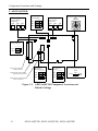
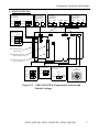
1
AD12-16(PCI)E
AD12-16U(PCI)E
AD16-16(PCI)E
Analog Input Board for PCI
User’s Guide
Copyright
Copyright 1997 CONTEC Co., LTD. ALL RIGHTS RESERVED
No part of this document may be copied or reproduced in any form
by any means without prior written consent of CONTEC Co., LTD.
CONTEC MICROELECTRONICS makes no commitment to
update or keep current the information contained in this document.
The information in this document is subject to change without
notice.
All relevant issues have been considered in the preparation of this
document. Should you notice an omission or any questionable
item in this document, please feel free to notify CONTEC Co.,
LTD.
Regardless of the foregoing statement, CONTEC assumes no
responsibility for any errors that may appear in this document nor
for results obtained by the user as a result of using this product.
Trademarks
MS, Microsoft, MS-DOS and Windows are trademarks of Microsoft
Corporation. Other brand and product names are trademarks of their
respective holder.
AD12-16(PCI)E, AD12-16U(PCI)E, AD16-16(PCI)E
i
Product Configuration
- AD12-16(PCI)E, AD12-16U(PCI)E or
AD16-16(PCI)E Board…1
- AD12-16(PCI)E, AD12-16U(PCI)E and AD16-16(PCI)E boards
User’s Manual (this booklet)…1
- Setup Disk (3½ inch 2HD)…1
Unpacking
The board is specially packed in an anti-static plastic bag to prevent
damage during shipment.
Check the contents to make sure that you have everything listed
above. If you do not have all the items, contact CONTEC.
Notes!
- Do not remove the board from its protective packaging until the
computer is open and you are ready to install. Static can be
very damaging to all electronic components.
- Optional software driver and connection products are available
from CONTEC. Call for more information.
ii
AD12-16(PCI)E, AD12-16U(PCI)E, AD16-16(PCI)E
Table of Contents
Copyright ............................................................................i
Trademarks ........................................................................i
Product Configuration ..................................................... ii
1. Introduction ............................................................. 1
About the Boards ..........................................................1
Features.........................................................................1
Limited Three Year Warranty ......................................3
How to Obtain Service ..................................................3
Liability .........................................................................3
About this Manual ........................................................4
2. Component Locations and Settings ............................ 5
Component Locations and Default Settings ....................5
Analog Input Settings.................................................10
Analog Output Setting ...............................................13
Set Counter and Digital I/O .......................................14
3. Board Setup ........................................................... 15
Use CONTEC Windows Software Products...................15
When Not Using CONTEC Software for Windows .......16
For Windows 98 Systems............................................16
For Windows 95 Systems............................................19
For other OS systems .................................................24
4. External Connections .............................................. 25
External Connections .................................................25
Signal Connection .......................................................28
Analog Output Connection .........................................31
Digital I/O Connection................................................32
AD12-16(PCI)E, AD12-16U(PCI)E, AD16-16(PCI)E
iii
5. Operation Functions ............................................... 33
Analog Input Function (A/D)......................................33
Analog Output Function (D/A) ...................................45
Digital Input Function [DI] ........................................46
Digital Output Function [DO]....................................46
Counter Function........................................................46
Interrupt Function......................................................48
6. Demonstration Program .......................................... 49
7. Calibration Program ............................................... 53
8. System Reference.................................................... 57
Specifications ..............................................................57
Timing of External Control Signals ...........................62
9. Troubleshooting ...................................................... 63
10. Index ................................................................... 65
iv
AD12-16(PCI)E, AD12-16U(PCI)E, AD16-16(PCI)E
List of Figures
Figure 2.1.
AD12-16(PCI)E Component Locations and Default
Settings..................................................................... 6
Figure 2.2.
AD12-16U(PCI)E Component Locations and Default
Settings..................................................................... 7
Figure 2.3.
AD16-16(PCI)E Component Locations and Default
Settings..................................................................... 8
Figure 2.4.
Board ID Setting (SW1) ........................................... 9
Figure 2.5.
Setting the Interrupt Use........................................... 9
Figure 2.6.
Setting Input Mode................................................. 10
Figure 2.7.
AD12-16(PCI)E’s Input Range Settings ..................11
Figure 2.8.
AD12-16U(PCI)E’s Input Range Settings ...............11
Figure 2.9.
AD16-16(PCI)E’s Input Range Settings ................. 12
Figure 2.10. AD12-16(PCI)E’s Output Range Settings............... 13
Figure 2.11. AD12-16U(PCI)E’s Output Range Settings............ 13
Figure 2.12. AD16-16(PCI)E’s Output Range Settings............... 13
Figure 2.13. Jump the CN2 Pin10 as DO3 or CNT Output ......... 14
Figure 2.14. Select Gate Signal of Counter 1 and 2 .................... 14
Figure 2.15. Select Clock Signal of Counter............................... 14
Figure 4.1.
CN1 Signal Configuration...................................... 25
Figure 4.2.
CN2 Signal Configuration...................................... 26
Figure 4.3.
Single-ended Input Connection (Flat Cable) ........... 28
Figure 4.4.
Single-ended Input Connection (Shield Cable) ....... 28
Figure 4.5.
Differential Input Connection (Flat Cable) ............. 29
Figure 4.6.
Differential Input Connection (Shield Cable) ......... 29
Figure 4.7.
Analog Output Connection (Flat Cable) ................. 31
AD12-16(PCI)E, AD12-16U(PCI)E, AD16-16(PCI)E
v
Figure 4.8.
Analog Output Connection (Shield Cable).............. 31
Figure 4.9.
Digital Input Connection ........................................ 32
Figure 4.10. Digital Output Connection...................................... 32
Figure 5.1.
Single Channel Mode Operation............................. 34
Figure 5.2.
Multichannel Mode Operation................................ 34
Figure 5.3.
Example of Sampling Clock Error of Single Channel
............................................................................... 35
Figure 5.4.
Example of Sampling Clock Error of Multichannels
............................................................................... 35
Figure 5.5.
Converted Data Comparison Conditions for Starting
Sampling ................................................................ 36
Figure 5.6.
Converted Data Comparison Conditions for Stopping
Sampling ................................................................ 38
Figure 5.7.
Controlling Number of Samplings.......................... 39
Figure 5.8.
Number of Repeats................................................. 40
Figure 5.9.
FIFO Format Buffer Memory ................................. 41
Figure 5.10. Ring Format Buffer Memory.................................. 43
Figure 5.11. Timing Diagram for the Analog Output Operation . 45
Figure 5.12. Digital Input ........................................................... 46
Figure 5.13. Digital Output ........................................................ 46
Figure 5.14. Counter Configuration............................................ 47
Figure 7.1.
Instruments for Calibration..................................... 53
Figure 8.1.
Block Diagram ....................................................... 61
Figure 8.2.
Timing Chart of External Sampling Clock.............. 62
Figure 8.3.
Timing Chart of External Sampling Start Trigger ... 62
Figure 8.4.
Timing Chart of External Sampling Stop Trigger ... 62
vi
AD12-16(PCI)E, AD12-16U(PCI)E, AD16-16(PCI)E
List of Tables
Table 5.1. Input Range and Coefficient...................................... 43
Table 5.2. Examples of Converted Data
(+/-10V range/Input gain = 1)................................. 44
Table 5.3. Examples of Output Voltages and Their Digital Data
(12-bit) ................................................................... 45
Table 5.4. Example of Jumper Settings for Counter................... 47
Table 5.5. Interrupt Request Signal Events ................................ 48
Table 6.1.
Contents of the Diskette............................................ 49
Table 7.1.
AD12-16(PCI)E’s Potentiometers for
Analog Input Circuit............................................... 54
Table 7.2.
AD12-16U(PCI)E’s Potentiometers for
Analog Input Circuit............................................... 54
Table 7.3.
AD16-16(PCI)E’s Potentiometers for
Analog Input Circuit............................................... 54
Table 7.4. Potentiometers for Analog Output Circuits of
AD12-16(PCI)E ..................................................... 55
Table 7.5. Potentiometers for Analog Output Circuits of
AD12-16U(PCI)E................................................... 55
Table 7.6. Potentiometers for Analog Output Circuits of
AD16-16(PCI)E ..................................................... 55
Table 8.1.
AD12-16(PCI)E ........................................................ 57
Table 8.2.
AD12-16U(PCI)E ..................................................... 58
Table 8.3.
AD16-16(PCI)E ........................................................ 59
Table 8.4.
Common to All of the three boards ........................... 60
Table 8.5. Timing Table of External Control Signals ................. 62
AD12-16(PCI)E, AD12-16U(PCI)E, AD16-16(PCI)E
vii
viii
AD12-16(PCI)E, AD12-16U(PCI)E, AD16-16(PCI)E
Introduction
1. Introduction
About the Boards
The AD12-16(PCI)E, AD12-16U(PCI)E and AD16-16(PCI)E
boards are multifunction IBM PC add-on interface boards. The
boards convert analog signals to digital data (A/D) and convert
digital data to analog signals (D/A). In addition, they supply four
digital input channels and four digital output channels. These
boards feature a 256K-word on board memory to maximize the A/D
conversion speed. The boards also support interrupt operations.
The AD12-16(PCI)E and AD12-16U(PCI)E are a 12-bit A/D and
D/A conversion resolution.
The AD16-16(PCI)E is a 16-bit A/D and D/A conversion
resolution.
Features
- Up to 1µsec A/D speed (1MHz) of AD12-16U(PCI)E
Up to 10µsec A/D speed (100KHz) of AD12-16(PCI)E
and AD16-16(PCI)E
- 16-bit resolution of AD16-16(PCI)E
12-bit resolution of AD12-16(PCI)E
and AD12-16U(PCI)E
- 16 single-ended analog inputs or 8 differential analog inputs
(Up to 32 single-ended or 16 differential inputs can be
expandable through an optional terminal unit).
- 256K-word on board memory to maximize A/D sampling speeds
and enable background processing.
This buffer memory can be used either by FIFO method or by
ring method.
- Various A/D sampling control functions.
Start or stop a sampling (A/D) not only by software but also by
value of the analog signal or by detecting a TTL level external
signal. The sampling clock that determines the sampling speed
can be selected from the on board clock or from an external clock
signal.
- 1-channel analog output
- Four TTL level digital input and four TTL level digital output
channels.
AD12-16(PCI)E, AD12-16U(PCI)E, AD16-16(PCI)E
1
Introduction
- One i8254 compatible counter
- Various interrupt events such as end of sampling, change in
external signal, error detected, and so on.
- A lot of optional products
ATSS-16: simultaneous sampling/hold terminal unit.
ATII-8:
electrically isolated conditioning terminal unit with
CJC circuit and current input function.
ATLF-8: differential input conditioning terminal unit with
lowpass filter function.
ATCH-16(PCI) and ATUH-16(PCI): input channel expanding
erminal units.
DTP-3(PC) and FTP-15: easy connecting screw terminal units.
ATP-16: BNC connector terminal unit for single-ended inputs.
PCC16PS: coaxial cable for single-ended input.
PCD8PS: two-wire shield cable for differential input.
Note!
To operate the AD12-16(PCI)E, AD12-16U(PCI)E and AD1616(PCI)E boards, an optional software driver is needed. Call
your dealer for more information about this software driver.
For further information, see page 57 of "System Reference".
2
AD12-16(PCI)E, AD12-16U(PCI)E, AD16-16(PCI)E
Introduction
Limited Three Year Warranty
CONTEC interface boards are warranted by CONTEC Co., LTD. to
be free from defects in material and workmanship for up to three
years from the date of purchase by the original purchaser.
Repair will be free of charge only when this device is returned
freight prepaid with a copy of the original invoice and a Return
Merchandise Authorization to the distributor or the CONTEC group
office, from which it was purchased.
This warranty is not applicable for scratches or normal wear, but
only for the electronic circuitry and original board. It is also not
applicable if the device has been tampered with or damaged through
abuse, mistreatment, neglect or unreasonable use, or if the original
invoice is not included, in which case repairs will be considered
beyond the warranty policy. If a replacement with a new device is
needed, regular factory prices will be charged, and the product will
be returned to you COD, and no other written warranty will apply.
The obligation of the warrantor is solely to repair or replace the
product. In no event will the warrantor be liable for any incidental
or consequential damages due to such defect or consequences that
arise from inexperienced usage, misuse, or malfunction of this
device.
How to Obtain Service
For replacement or repair, return the device freight prepaid, with a
copy of the original invoice. Please obtain a Return Merchandise
Authorization Number (RMA) from the CONTEC group office
where you purchased before returning any product.
* No product will be accepted by CONTEC group without the
RMA number.
Liability
The obligation of the warrantor is solely to repair or replace the
product. In no event will the warrantor be liable for any incidental
or consequential damages due to such defect or consequences that
arise from inexperienced usage, misuse, or malfunction of this
device.
AD12-16(PCI)E, AD12-16U(PCI)E, AD16-16(PCI)E
3
Introduction
About this Manual
This manual provides instructions for setting up and using the
AD12-16(PCI)E, AD12-16U(PCI)E and AD16-16(PCI)E boards.
It is divided into seven main sections: Setup, External Connection,
Operation Functions, Demonstration Programs, Calibration, System
Reference, and Troubleshooting.
Chapter 1
Introduction
Chapter 2
Component Locations and Settings
contains all the information necessary to setup the
AD12-16(PCI)E, AD12-16U(PCI)E and
AD16-16(PCI)E boards.
Chapter 3
Board Setup
Explains how to set up the board
Chapter 4
External connection
details the signal assignment of the external connectors
and gives some connecting examples.
Chapter 5
Operation Functions
explains the basic operation function of this board.
Chapter 6
Demonstration Programs
explains the basic use of demonstration programs for
MS-DOS.
Chapter 7
Calibration
contains the method of calibration and equipments.
Chapter 8
System Reference
contains the specifications for each of AD12-16(PCI)E,
AD12-16U(PCI)E and AD16-16(PCI)E boards.
Chapter 9
Troubleshooting
is a series of questions to ask yourself and steps to take
to solve problems on your own. It also includes a
checklist to fill out before calling CONTEC for help.
All addresses and examples are written in Hexadecimal.
4
AD12-16(PCI)E, AD12-16U(PCI)E, AD16-16(PCI)E
Component Locations and Settings
2. Component Locations and Settings
This section covers everything from getting an AD12-16(PCI)E,
AD12-16U(PCI)E or AD16-16(PCI)E boards out of the box to
plugging it into your computer.
The following installation procedure is for the AD12-16(PCI)E,
AD12-16U(PCI)E and AD16-16(PCI)E boards only and does not
include instructions for any accessories.
Component Locations and Default Settings
The AD12-16(PCI)E, AD12-16U(PCI)E and AD16-16(PCI)E
boards are shipped from the factory with the following settings:
AD12-16(PCI)E, AD12-16U(PCI)E, AD16-16(PCI)E
5
Component Locations and Settings
1. AD12-16(PCI)E:
VR5
VR4
For Analog
Input Signal
Adjusting
JP8
VR3
VR2
For Setting Board Address
SW1
BOARD
VR1
23
JP9
7 9
BCDE
A
VR6
For Setting
Input Range
1 2 3
JP7
4 56
For Analog
Output Signal
Adjusting
F01
1 2 3
For Output
Setting Range
1 2 3
JP10
JP11
1 2 3
CN1 Analog Signal
I/O Connector
CN2 Digital and Control
Signal I/O Connector
CN3 Channel Exapanding
Unit Connector
For Input
Mode Setting
1 2 3
JP4
For Counter
Setting
1 2 3
JP1
JP5
JP2
JP6
JP12
INT
USE
1 2 3
JP3
1 2 3
Jumper for Setting
Interrupt Signal Resource
1 2 3
Figure 2.1. AD12-16(PCI)E Component Locations and
Default Settings
6
AD12-16(PCI)E, AD12-16U(PCI)E, AD16-16(PCI)E
NOT
USE
Component Locations and Settings
2. AD12-16U(PCI)E:
For Setting
Input Range
1 2 3
1 2 3
JP7
JP9
JP8
JP10
1 2 3
For Analog
Input Signal
Adjusting
For Analog
Input Signal
Adjusting
VR1
VR3
VR2
VR4
For Analog
Output Signal
Adjusting
VR8
VR9
VR5
VR6
VR7
1 2 3
For Input
Mode Setting
1 2 3
JP4
JP5
JP6
1 2 3
CN1 Analog Signal
I/O Connector
CN2 Digital and Control
Signal I/O Connector
CN3 Channel Exapanding
Unit Connector
1 2 3
JP3
1 2 3
SW1
BOARD ID
JP13
INT
USE
1 2 3
NOT
USE
4 56
JP12
For Setting Board Address
7 9
23
JP2
Jumper for Setting
Interrupt Signal
Resource
F 01
For Output
Setting Range
1 2 3
JP11
B C DE
A
For Counter
Setting
1 2 3
JP1
Figure 2.2. AD12-16U(PCI)E Component Locations and
Default Settings
AD12-16(PCI)E, AD12-16U(PCI)E, AD16-16(PCI)E
7
Component Locations and Settings
3. AD16-16(PCI)E:
1 2 3
For Analog
Output Adjusting
VR6
JP7
VR5
VR4
JP11
JP9
For Analog
Input Adjusting
VR3
VR2
7 9
2
JP10
VR1
SW1
BOARD ID
F 01
1 2 3
B C DE
A
VR7
For Setting Board Address
JP8
1 2 3
3 4 56
For Setting
Input Range
1 2 3
For Analog
Input Adjusting
VR11
VR10
VR9
VR8
CN1 Analog Signal
I/O Connector
CN2 Digital and Control
Signal I/O Connector
CN3 Channel Exapanding
Unit Connector
For Input
Mode Setting
For Output
Range Setting
1 2 3
JP4
1 2 3
JP12
JP5
JP6
1 2 3
For Counter
Setting
1 2 3
JP1
JP13
JP2
JP14
JP3
Jumper for Setting
Interrupt Signal
Resource
JP16
INT
USE
1 2 3
JP15
1 2 3
1 2 3
Figure 2.3. AD16-16(PCI)E Component Locations and
Default Settings
8
AD12-16(PCI)E, AD12-16U(PCI)E, AD16-16(PCI)E
NOT
USE
Component Locations and Settings
Setting the Board ID
If you install two or more boards of a same type on one personal
computer, set their respective board IDs to distinguish them.
Assign a different value to each of the boards.
The board IDs from 0 to F can be set to identify up to sixteen
boards.
Setting procedure
To set the board ID, use the rotary switch on the board. Turn the
SW1 knob to set the board ID as shown below.
2
7 9
B C DE
A
3 4 56
SW1
BOARD ID
Factory setting
(board ID=0)
F 01
Figure 2.4. Board ID Setting (SW1)
Setting the Interrupt use
If you don’t use the Interrupt function, to save the Interrupt
resources of PC, you can let recognize to the PC the AD1216(PCI)E, AD12-16U(PCI)E or AD16-16(PCI)E as no-interrupt
function board.
In case of interrupt use, this board is assigned the interrupt level
from PC.
Setup when interrupt is used
Setup when interrupt is not used
[AD12-16(PCI)E] uses JP12
[AD12-16U(PCI)E] uses JP13
[AD16-16(PCI)E] uses JP16
[AD12-16(PCI)E] uses JP12
[AD12-16U(PCI)E] uses JP13
[AD16-16(PCI)E] uses JP16
INT
USE
INT
NOT USE
1 2 3
USE
NOT USE
1 2 3
Figure 2.5. Setting the Interrupt Use
AD12-16(PCI)E, AD12-16U(PCI)E, AD16-16(PCI)E
9
Component Locations and Settings
Analog Input Settings
Analog input settings include input mode setting and input range
setting.
Set Input Mode
Input mode setting selects the input signal connection method.
Jumpers JP4, JP5 and JP6 are used for setting the input mode. All
the AD12-16(PCI)E, AD12-16U(PCI)E and AD16-16(PCI)E share
the same settings. The following figure shows how to set the input
mode.
Single-Ended Input
Differential Input
JP4
JP4
1 2 3
JP5
1 2 3
JP5
1 2 3
JP6
1 2 3
JP6
1 2 3
1 2 3
Figure 2.6. Setting Input Mode
Note!
Do not set the jumper at any other setting.
malfunction.
It may be cause of
Set Input Range
Input range setting selects a voltage range of analog input signals.
The board converts the signal within the range into a digital data
according to the resolution. The input range is the same for all
input channels. You cannot set individual input range for each
channel. Figures 2.7. , 2.8. and 2.9. show the jumper settings of
the boards.
10
AD12-16(PCI)E, AD12-16U(PCI)E, AD16-16(PCI)E
Component Locations and Settings
AD12-16(PCI)E:
Bipolar -10V~+10V
Unipolar 0V~+10V
JP7
JP7
1 2 3
1 2 3
JP8
JP8
1 2 3
1 2 3
JP9
JP9
1 2 3
1 2 3
Figure 2.7. AD12-16(PCI)E’s Input Range Settings
AD12-16U(PCI)E:
Bipolar -5V~+5V
JP7
Bipolar -2.5V~+2.5V
JP9
1 2 3
JP8
JP7
1 2 3
JP10
1 2 3
JP8
1 2 3
Unipolar 0V~+10V
JP7
JP8
1 2 3
JP7
1 2 3
JP9
1 2 3
1 2 3
JP10
1 2 3
1 2 3
JP10
Unipolar 0V~+5V
JP9
1 2 3
JP9
1 2 3
JP8
1 2 3
1 2 3
JP10
1 2 3
1 2 3
Figure 2.8. AD12-16U(PCI)E’s Input Range Settings
AD12-16(PCI)E, AD12-16U(PCI)E, AD16-16(PCI)E
11
Component Locations and Settings
AD16-16(PCI)E:
Bipolar -10V~+10V
JP7
Bipolar -5V~+5V
JP8
1 2 3
JP7
1 2 3
JP11
JP8
1 2 3
1 2 3
JP11
1 2 3
JP10
1 2 3
JP9
1 2 3
JP10
1 2 3
Unipolar 0V~+10V
JP7
JP9
1 2 3
1 2 3
Unipolar 0V~+5V
JP8
JP7
1 2 3
1 2 3
JP11
JP8
1 2 3
1 2 3
JP11
1 2 3
JP10
1 2 3
JP9
1 2 3
JP10
1 2 3
JP9
1 2 3
1 2 3
Figure 2.9. AD16-16(PCI)E’s Input Range Settings
12
AD12-16(PCI)E, AD12-16U(PCI)E, AD16-16(PCI)E
Component Locations and Settings
Analog Output Setting
Use jumpers to select an analog output voltage range.
Set output range
Figures 2.10. , 2.11. and 2.12. show the jumper settings of various
output voltage ranges.
AD12-16(PCI)E:
Bipolar -10V~+10V
JP10
Bipolar -5V~+5V
JP10
1 2 3
JP11
Unipolar 0V~+10V
JP10
1 2 3
JP11
1 2 3
1 2 3
JP11
1 2 3
1 2 3
Figure 2.10. AD12-16(PCI)E’s Output Range Settings
AD12-16U(PCI)E:
Bipolar -10V~+10V
JP11
Bipolar -5V~+5V
JP11
1 2 3
JP12
Unipolar 0V~+10V
JP11
1 2 3
JP12
1 2 3
1 2 3
JP12
1 2 3
1 2 3
Figure 2.11. AD12-16U(PCI)E’s Output Range Settings
AD16-16(PCI)E:
Bipolar -10V~+10V
JP12
Unipolar 0V~+10V
JP12
1 2 3
JP13
1 2 3
JP13
1 2 3
JP14
1 2 3
JP14
1 2 3
1 2 3
JP15
JP15
1 2 3
1 2 3
Figure 2.12. AD16-16(PCI)E’s Output Range Settings
Note!
Do not set the jumper to other setting.
malfunction.
Doing so may cause a
AD12-16(PCI)E, AD12-16U(PCI)E, AD16-16(PCI)E
13
Component Locations and Settings
Set Counter and Digital I/O
The AD12-16(PCI)E, AD12-16U(PCI)E and AD16-16(PCI)E
boards have integrated an i8254 compatible counter into its circuit.
Because some digital I/O signals share the same connector pins
with these counter signals, this section shows you how to set the
jumpers for the control and output signals (counter output signal,
gate signal, clock input signal) of this counter.
Jumper JP1 is used to select an output signal for connector
CN2’s pin 10.
JP1
Digital Output 3
DO3
Counter Output
CNT Output
1 2 3
JP1
1 2 3
Figure 2.13. Jump the CN2 Pin10 as DO3 or CNT Output
Jumper JP2 is used to select the gate control signal of the i8254
either from the internal circuit or from the connector
CN2’s pin 4, the DI1/CNT Gate signal.
JP2
Internal Signal
8254Gate
External Signal
Digital Input 1 / CNT Gate
1 2 3
JP2
1 2 3
Figure 2.14. Select Gate Signal of Counter 1 and 2
Jumper JP3 is used to set the clock signal of the i8254’s counter 1
either as the count output of the i8254’s counter 0 or from the
connector CN2’s pin 12, the DI2/CNT Clock signal.
Counter0 Output Signal
JP3
1 2 3
External Signal
JP3
DI 12 / CNT Clock
1 2 3
Figure 2.15. Select Clock Signal of Counter
Note!
Only TTL level signals can be used for the counters.
14
AD12-16(PCI)E, AD12-16U(PCI)E, AD16-16(PCI)E
Board Setup
3. Board Setup
The board setup method varies according to the operating system
being used.
Use CONTEC Windows Software Products
For MS Windows OS systems, we recommend you to use our
Windows software products (optional).
< Examples of CONTEC software products for Windows>
- Driver Software Package (Option)
API-PAC(W32)
- ActiveX Component Package (Option)
ACX-PAC(W32)
Please follow the setup instructions of the User’s manual shipped
with the software products and/or the help files of the package to
setup our interface board(s) to your system.
For details of CONTEC software products, please contact our sales
agencies.
AD12-16(PCI)E, AD12-16U(PCI)E, AD16-16(PCI)E
15
Board Setup
When Not Using CONTEC Software for Windows
When you don't use CONTEC software for Windows, the board
setup procedure varies with each OS.
For Windows 98 Systems
Every PCI bus board/device will be automatically assigned required
system resources, such as I/O address range and interrupt level, by
the system whenever the system is turned on.
Under Windows 98 OS, before using the board you should register
the board information, such as assigned resources, to the OS. This
procedure is called hardware installation. After the hardware
installation is done, Windows 98 can then manage the board
information from its registers.
Following is hardware installation steps. After finished the
installation, you are supposed to confirm the registered board
information from Windows 98 registers.
This procedure does not install board driver(s).
install driver program(s) yourself.
Lately you should
Hardware Installation Steps
(1) Set the board ID.
(2) Be sure the power of the personal computer is turned off; then
plug the board into a PCI bus slot in the system.
(3) Turn the personal computer ON to start up Windows 98.
(4) Because this is the first time Windows 98 detected the board
from the system, Windows 98 will display a message of [New
Hardware] on the screen and start run an [Add New Hardware
Wizard] program. After you find a massage of [PCI
Multimedia Device] from the program window, click [Next>]
to continue.
(5) In the next dialog box, select a radio button of [Search for the
best driver for your device. (Recommended).], then click
[Next>] to continue.
(6) In the next dialog box, select both of the [Floppy disk drives
(F)] and [Specify Location (L)] check boxes, then enter the
16
AD12-16(PCI)E, AD12-16U(PCI)E, AD16-16(PCI)E
Board Setup
drive name, such as "A:", and the directory name, WIN95, into
the [Location] field.
Insert the attached FD into the disk drive, then click [Next>] to
continue.
(7) In the [Windows driver file search for the device] dialog box,
check that "CONTEC Co., Ltd.-Board Name" and
"AIO_PI0.INF" in the [Location of driver] has been listed,
then click [Next>] to continue.
(8) In the next dialog box, you will find a message of "Windows
has finished installing the software that your new hardware
device requires." Then you click [Finish] to complete the
installation of the board. After completed the board
installation, you are supposed to confirm the registered board
information from Windows 98 registers. The "Checking
resources" part of this section explains you how to do it.
Method of installing two or more boards:
(1) Install the first board correctly.
(2) Be sure to complete installation of the first board before
attempting to install a second one.
(3) Exit Windows 98 and turn the personal computer off.
(4) Set the board ID of the second board that should be different
from the first one. Then plug the board into a PCI bus slot.
(5) Turn the personal computer on and start the Windows 98 again.
(6) Windows 98 will display a massage of [New Hardware] on the
screen and start run an [Add New Hardware Wizard] program.
After you find a massage of [CONTEC Co., Ltd.-Board Name]
from the program window, click [Next>] to continue.
(7) In the next dialog box, select a radio button of [Display a list
of all the drivers in a specific location, so you can select the
driver you want.], then click [Next>] to continue.
(8) From the [Models] window, select "CONTEC Co., Ltd.Board Name" and click [Next>] to continue.
(9) In the [Windows driver file search for the device] dialog box,
there should be the message of "CONTEC Co., Ltd.-Board
AD12-16(PCI)E, AD12-16U(PCI)E, AD16-16(PCI)E
17
Board Setup
Name" and "CONTEC~*.INF" in the [Location of driver]
window, after confirmed this message click [Next>] to
continue. (A number which is assigned by the OS will
replace the "*" mark.)
(10) In the next dialog box, you will find a message of "Windows
has finished installing the software that your new hardware
device requires." Then you click [Finish] to complete the
installation of the board. After completed the board
installation, you are supposed to confirm the registered board
information from Windows 98 registers again.
For installing the third board and any additional boards, follow the
same steps as those for installing a second board. Before you can
install a third board or additional boards, all the boards that are
already installed must be in their PCI bus slots.
Notes!
- The second board cannot be properly installed unless the
resources (I/O addresses and interrupt level) for the board can
be allocated. Before attempting to install the second board,
first determine what PC resources are free to use.
- The resources used by each board do not depend on the location
of the PCI bus slot or the board itself. If you remove two or
more boards that have already been installed and then remount
one of them on the computer, it is unknown that which one of the
sets of resources previously assigned to the two boards is
assigned to the remounted board. In this case, you must check
the resource settings.
Checking resources
Follow the steps below to check the assigned resources managed by
the OS.
(1) Double-click on the [System] option in [Control Panel] to open
the [System Properties] property sheet. Select the [Device
Manager] tab.
(2) Click [Multi-function adapters] folder.
(3) Click [CONTEC Co., Ltd.-Board Name] folder to display its
properties.
(4) Select the [Resources] tab to check the device type, resource
settings, and the conflicting device list.
18
AD12-16(PCI)E, AD12-16U(PCI)E, AD16-16(PCI)E
Board Setup
For Windows 95 Systems
Every PCI bus board/device will be automatically assigned required
system resources, such as I/O address range and interrupt level, by
the system whenever the system is turned on.
Under Windows 95 OS, before using the board you should register
the board information, such as assigned resources, to the OS. This
procedure is called hardware installation. After the hardware
installation is done, Windows 95 can then manage the board
information from its registers.
Following is hardware installation steps. After finished the
installation, you are supposed to confirm the registered board
information from Windows 95 registers.
This procedure does not install board driver(s).
install driver program(s) yourself.
Lately you should
Procedure of Hardware Installation
<Checking the OS version>
The procedure of installing the board is different from the
Windows 95 versions. Before any installation, you must check the
version of Windows 95 that you are using.
(1) Open [Control Panel] from [My Computer].
(2) Double-click on the [System] option to open the [System
Properties] property sheet.
(3) Check the "System:" number displayed on the [General] page.
System :
Microsoft Windows 95
4.00.950
The versions of Windows 95 include 4.00.950, 4.00.950a,
4.00.950B and 4.00.950C. The board setup method depends on
the version of Windows 95 that is being used.
AD12-16(PCI)E, AD12-16U(PCI)E, AD16-16(PCI)E
19
Board Setup
For Windows 95 version 4.00.950 or 4.00.950a systems:
(1) Set the board ID.
(2) Be sure the power of the personal computer is turned off; then
plug the board into a PCI bus slot in the system.
(3) Turn the personal computer ON to start up Windows 95.
(4) Windows 95 will come up with the [New Hardware] detection
dialog box. Select [Multimedia Device: Select which driver
you want to install for your new hardware.] and then [Driver
from disk provided by hardware manufacturer].
(5) In the [Install From Disk] dialog box, insert the attached FD
into the disk drive, enter the drive name and directory name in
the [Copy Distributed File From] field, then click [OK].
This completes installation of the board.
(6) Follow the instructions on the screen to complete installation
of the board. After completed the board installation, you are
supposed to confirm the registered board information from
Windows 95 registers. The "Checking resources" part of this
section explains you how to do it.
For Windows 95 version 4.00.950B or 4.00.950C systems:
(1) Set the board ID.
(2) Be sure to check that the personal computer is off; then plug
the board into a PCI bus slot in the system.
(3) Turn the personal computer on to start up Windows 95.
(4) Because this is the first time Windows 95 detected the board
from the system, Windows 95 will display a message of [New
Hardware] on the screen and start run an [Device Driver
Wizard] program. After you find a massage of [PCI
Multimedia Device] from the program window, click [Next>]
to continue.
(5) In the next dialog box, select [Specify Location...]. Insert the
attached FD into a drive, enter the drive name and directory
name (WIN95) in the [Location] field, then click [OK].
(6) In the next dialog box, there should be a message of "Updated
driver found for this device". After confirmed this message
20
AD12-16(PCI)E, AD12-16U(PCI)E, AD16-16(PCI)E
Board Setup
you click [End]. This completes installation of the board.
After completed the board installation, you are supposed to
confirm the registered board information from Windows 95
registers. The "Checking resources" part of this section
explains you how to do it.
Method of installing two or more boards
(For Windows 95 version 4.00.950 or 4.00.950a system) :
(1) Install the first board correctly.
(2) Be sure to complete installation of the first board before
attempting to install the second one.
(3) Exit Windows 95 and turn the personal computer off.
(4) Check the board ID of the second board that should be
different from the first one. Then plug the board into a PCI
bus slot.
(5) Turn the personal computer on again to start up Windows 95.
(6) Windows 95 will come up with the [New Hardware] detection
dialog box. In [Multimedia Device: Select which driver you
want to install for your new hardware.], select [Select from
List].
(7) The [Select Hardware Type] dialog box will then appear.
In [Select Hardware Type to Install] windows, select [Other
Devices].
(8) In the [Select Device] dialog box, select [CONTEC] from
[Manufacturers] window and select [CONTEC Co., Ltd.-Board
Name] from [Models] window.
(9) A [Change System Settings] dialog box appears.
messages to restart the computer.
Follow the
(10) When Windows 95 is restarted, installation of the second board
is completed. Check the assigned resources again.
For installing the third board and any additional boards, follow the
same steps as those for installing a second board. Before you can
install a third board or additional boards, all the boards that are
already installed must be in PCI bus slots.
AD12-16(PCI)E, AD12-16U(PCI)E, AD16-16(PCI)E
21
Board Setup
Notes!
- The second board cannot be properly installed unless the
resources (I/O addresses and interrupt level) for the board can
be allocated. Before attempting to install the second board,
first determine what PC resources are free.
- The resources used for each board do not depend on the location
of the PCI bus slot or the board itself. If you remove two or
more boards that have already been installed and then re-mount
one of them on the computer, it is unknown which one of the sets
of resources previously assigned to the two boards is assigned to
the re-mounted board. In this case, re-check the resource
settings.
Method of installing two or more Boards
(For Windows 95 version 4.00.950B or 4.00.950C systems) :
(1) Install the first board correctly.
(2) Be sure to complete installation of the first board before
attempting to install the second one.
(3) Exit Windows 95 and turn the personal computer OFF.
(4) Check the board ID of the second board, then plug it into a PCI
bus slot. Assign to the second board a board ID different
from the ID assigned to the first board.
(5) Turn the personal computer on again to start up Windows 95.
(6) The OS will then automatically install the second board.
When the installation has been completed, check the assigned
resources again.
For installing the third board and any additional boards, follow the
same steps as those for installing a second board. Before you can
install a third board or additional boards, all the boards that are
already installed must be in PCI bus slots.
Notes!
- The second board cannot be properly installed unless the
resources (I/O addresses and interrupt level) for the board can
be allocated. Before attempting to install a second board, first
determine which PC resources are free.
- The resources used for each board do not depend on the location
of the PCI bus slot or the board itself. If you remove two or
22
AD12-16(PCI)E, AD12-16U(PCI)E, AD16-16(PCI)E
Board Setup
more boards that have already been installed and then re-mount
one of them on the computer, it is unknown which one of the sets
of resources previously assigned to the two boards is assigned to
the re-mounted board. In this case, re-check the resource
settings.
Checking resources
Follow the steps below to check the assigned resources managed by
the OS.
(1) Double-click on the [System] option in [Control Panel] to open
the [System Properties] property sheet. Select the [Device
Manager] tab.
(2) Click on the [Multi-function adapters] folder.
(3) Click on the [CONTEC Co., Ltd.-Board Name] folder to
display its properties.
(4) Select the [Resources] tab to check the device type, resource
settings, and the conflicting device list.
AD12-16(PCI)E, AD12-16U(PCI)E, AD16-16(PCI)E
23
Board Setup
For other OS systems
We use MS-DOS as an example to show how to use the board under
other operation systems, in addition of the Windows OS.
Refer the MS-DOS programs in the attached FD.
For a PCI bus board, the system will automatically assign usable
resources to the board. Refer the following procedure to confirm
the assigned resources.
Procedure
(1) Set the board ID.
(2) Be sure that the personal computer is off; then plug the board
into a PCI bus slot in the personal computer.
(3) Turn the personal computer ON to start up MS-DOS.
(4) Copy the programs that are under the DOS directory of the
attached FD to a directory of your HDD.
(5) Execute the AIOPCI.EXE resource confirmation program.
(6) Check the I/O addresses and interrupt level (IRQ) displayed on
the screen.
Note!
When you use the board under a non plug-and-play OS like MSDOS, be sure that [PnP OS] is either [disabled] or set to [not to
use] in the PC's BIOS setup. If this is set to [Windows 95], for
example, the board might not be recognized properly.
24
AD12-16(PCI)E, AD12-16U(PCI)E, AD16-16(PCI)E
External Connections
4. External Connections
External Connections
You are now ready to connect the wires that carry the signals from
the board.
A 37-pin D type female connector (CN1) interfaces the analog
signals to the appropriate external devices and a 16-pin male
connector (CN2) connects the digital I/O signals from the external
devices.
Note!
Connector CN3 is only for optional terminal units and is not
available for user connections.
Analog Signal Connection
Figure 16 shows the definition of the CN1 connector for all the
AD12-16(PCI)E, AD12-16U(PCI)E and AD16-16(PCI)E boards.
CN1
Description
Analog Input 0 / 0 [+]
Analog Input 8 / 0 [-]
Analog Input 1 / 1 [+]
Analog Input 9 / 1 [-]
Analog Input 2 / 2 [+]
Analog Input 10 / 2 [-]
Analog Input 3 / 3 [+]
Analog Input 11 / 3 [-]
Analog Input 4 / 4 [+]
Analog Input 12 / 4 [-]
Analog Input 5 / 5 [+]
Analog Input 13 / 5 [-]
Analog Input 6 / 6 [+]
Analog Input 14 / 6 [-]
Analog Input 7 / 7 [+]
Analog Input 15 / 7 [-]
Analog Output
Simultaneous Hold Output
+5V DC from PC
No.
1
2
3
4
5
6
7
8
9
10
11
12
13
14
15
16
17
18
19
1
2
3
4
5
6
7
8
9
10
11
12
13
14
15
16
17
18
19
20
21
22
23
24
25
26
27
28
29
30
31
32
33
34
35
36
37
No.
Description
20
21
22
23
24
25
26
27
28
29
30
31
32
33
34
35
36
37
Analog Ground
Analog Ground
Analog Ground
Analog Ground
Analog Ground
Analog Ground
Analog Ground
Analog Ground
Analog Ground
Analog Ground
Analog Ground
Analog Ground
Analog Ground
Analog Ground
Analog Ground
Analog Ground
Analog Ground
Digital Ground
Figure 4.1. CN1 Signal Configuration
Analog Input
The Analog Input 0~15 are the input channel names of single-ended
input. The Analog Input 0[+]~7[+] and the Analog Input 0[-]~
7[-] are the input channel names of differential input.
Analog Output
The Analog Output pin outputs a single-ended voltage signal.
AD12-16(PCI)E, AD12-16U(PCI)E, AD16-16(PCI)E
25
External Connections
Simultaneous Hold Output
This signal is a control signal for the optional ATSS-16 terminal unit.
Analog Ground
The Analog ground signal (common to the analog I/O signals)
Digital Ground
The Digital ground signal (common to the simultaneous sampling
signal and +5V power output)
+5V DC
This is the power supply line from your PC. The power capacity
is 3A.
Notes!
- Do not short the output signals to the analog ground, digital
ground and/or power line.
- Do not short the power line to the analog ground and/or digital
ground.
Digital Signal Connection
Figure 17 shows the definition of the CN2 connector for all the
AD12-16(PCI)E, AD12-16U(PCI)E and AD16-16(PCI)E boards.
Description
No.
Digital Output 0
Digital Output 2
Digital Ground
Digital Input 1 / CNT Gate
Digital Input 3 / INT Trigger
External Stop Trigger Input
Sampling Clock Output
+5V DC from PC
A1
A2
A3
A4
A5
A6
A7
A8
CN2
A1
A2
A3
A4
A5
A6
A7
A8
B1
B2
B3
B4
B5
B6
B7
B8
No.
Description
B1
B2
B3
B4
B5
B6
B7
B8
Digital Output 1
Digital Output 3 / CNT Output
Digital Input 0
Digital Input 2 / CNT Clock
External Start Trigger Input
External Sampling Clock Input
Digital Ground
Not Connected
Figure 4.2. CN2 Signal Configuration
Digital Output
Digital Output 0 - Digital Output 3 are TTL level digital output
signals.
Note!
The Digital Output 3 shares the same pin with the CNT Output
(counters output signal) so that only one of these two signals can be
outputted simultaneously.
26
AD12-16(PCI)E, AD12-16U(PCI)E, AD16-16(PCI)E
External Connections
Digital Input
Digital Input 0- Digital Input 3 are TTL level digital input signals.
Digital Input 1 is also used as CNT Gate (counter gate control input).
Digital Input 2 is also used as CNT Clock (counter clock input).
Digital Input 3 is also used as INT Trigger (interrupt trigger input).
A/D Control Signals
External Start Trigger Input is a TTL level input signal and can start
the analog input samplings.
External Stop Trigger Input is a TTL level input signal and can used
to end the analog input samplings.
External Sampling Clock Input is also a TTL level clock signal for
the analog to digital converting operation.
Sampling Clock Output outputs the sampling clock of the analog
input circuit and is also be a TTL level signal.
Digital Ground
Digital ground commons to all digital signals and power output.
+5V DC
Power output line from your PC. The power capacity is 1A.
Notes!
- Do not short the output signals to the analog ground, digital
ground and/or power line.
- Do not short the power line to the analog ground and/or digital
ground.
AD12-16(PCI)E, AD12-16U(PCI)E, AD16-16(PCI)E
27
External Connections
Signal Connection
Analog Input Connection
There are two analog input mode: the Single-ended input and the
Differential input. Here we give some examples of analog input
connections by using flat cable or shield cable.
Single-ended Input
The following figure shows an example of flat cable connection.
Each signal source is connected to one analog input channel and the
signal common to analog ground pin of CN1.
BOARD
CN1
Cable
Signal Source
Analog Input 0..15
V
Analog Ground
Figure 4.3. Single-ended Input Connection (Flat Cable)
The following figure shows an example of shield cable connection.
When the distance between the signal source and the board is long
or you want to increase the noise tolerance, a shield cable is
suggested. Connect the signal by the core wire and common
signal by the shield braids.
BOARD
CN1
Shield cable
Signal Source
Analog Input 0..15
Analog Ground
V
Figure 4.4. Single-ended Input Connection (Shield Cable)
28
AD12-16(PCI)E, AD12-16U(PCI)E, AD16-16(PCI)E
External Connections
Notes!
- If the signal source contains over 1MHz signals, the signal may
effect the cross-talk noise between channels.
- If the board and the signal source receive noise or the distance
between the board and the signal source is too long, data may
not be input properly.
- An input analog signal should not exceed the maximum input
voltage (relate to the board analog ground). If it exceeds the
maximum voltage, the board may be damaged.
- Connect all the unused analog input channels to analog ground.
Differential Input
The following figure shows an example of flat cable connection.
Each signal source is connected to a [+] pin of analog input channel
and the signal common of this source to the [-] pin of this input
channel of CN1. In addition, the signal common must be
connected to the pin of the analog ground of CN1 by a third wire.
BOARD
CN1
Cable
Signal Source
Analog Input 0[+]..7[+]
V
Analog Input 0[-]..7[-]
Analog Ground
Figure 4.5. Differential Input Connection (Flat Cable)
The following figure shows an example of 2-wire shielded cable
connection. When the distance between the signal source and the
board is long or you want to increase the noise tolerance, a shield
cable connection is preferred. Each signal source is connected to a
[+] pin of analog input channel and the signal common of this
source to the [-] pin of this input channel of CN1. In addition, the
signal common must be connected to the pin of the analog ground
of CN1 by the shielded braids.
BOARD
CN1
Shield cable
Signal Source
Analog Input 0[+]..7[+]
Analog Input 0[-]..7[-]
V
Analog Ground
Figure 4.6. Differential Input Connection (Shield Cable)
AD12-16(PCI)E, AD12-16U(PCI)E, AD16-16(PCI)E
29
External Connections
Notes!
- If the signal source contains over 1MHz signals, the signal may
effect the cross-talk noise between channels.
- The input data would be uncertain If the analog ground is not
connected.
- If the board and the signal source receive noise or the distance
between the board and the signal source is too long, data may
not be input properly.
- The input voltage from the [+] input or [-] input should not
exceed the maximum input voltage (based on the board analog
ground). If it exceeds the maximum voltage, the board may be
damaged.
- Because the input data will be uncertain if the [+] pin or the [-]
pin of CN1 is not connected, all the unused input pins of CN1
should be connected to the analog ground, AGND.
30
AD12-16(PCI)E, AD12-16U(PCI)E, AD16-16(PCI)E
External Connections
Analog Output Connection
This section shows how to connect the analog output signal by
using a flat cable or a shielded cable.
The following figure shows an example of flat cable connection.
BOARD
CN1
Cable
Target
Analog Output
Digital multi meter
Analog Ground
Figure 4.7. Analog Output Connection (Flat Cable)
If the distance between the signal source and the board is long or if
you want to increase the noise tolerance, a shield cable connection
is strongly recommended.
BOARD
Analog Output
Analog Ground
CN1
Shield cable
Target
Digital multi meter
Figure 4.8. Analog Output Connection (Shield Cable)
Notes!
- If the board or the connected wire receives noise, or the distance
between the board and the target is long, data may not be
outputted properly.
- For analog output signal, the current capacity is ±5mA (Max.).
Check the specification of the connected device before
connecting the board.
- Do not short the analog output signal to analog ground, digital
ground, and/or power line. Doing so may damage the board.
AD12-16(PCI)E, AD12-16U(PCI)E, AD16-16(PCI)E
31
External Connections
Digital I/O Connection
The digital I/O signals and the control signals are interfaced through
the connector CN2. User can use an optional cable DT/E1 or
DT/E2 (with bracket and a 15-pin D type female connector) to
connect these signals to your external devices.
All the digital I/O signals and control signals are TTL level signals.
BOARD
CN2
Cable
Target
Input
Digital Ground
Figure 4.9. Digital Input Connection
BOARD
Output
I OL=24mA
CN2
Cable
Target
Digital Ground
Figure 4.10. Digital Output Connection
Note!
Do not short the output signals to analog ground, digital ground,
and/or power line. Doing so may damage the board.
32
AD12-16(PCI)E, AD12-16U(PCI)E, AD16-16(PCI)E
Operation Functions
5. Operation Functions
Here we are going to discuss some operation functions of AD1216(PCI)E, AD12-16U(PCI)E and AD16-16(PCI)E boards.
Analog Input Function (A/D)
This function converts analog signals to digital data depending on
the resolution. The converted data are stored in the on board
memory in the order of conversion. You can set conversion start
condition, stop condition, sampling period and other parameters for
your analog input function.
The following shows the parameters in general.
* Input channel / Input gain
--- Single channel
--- Multichannels
--- Input gain
--- Input gain
* Scan clock / Sampling clock
--- Scan clock
--- Scan clock
--- Internal clock
--- External clock signal
--- Input channel order
--- Sampling period
* Sampling start condition
--- Software
--- Converted data comparison --- Comparison condition --- No. of trigger delays
--- External signal rising edge --- No. of trigger delays
--- External signal falling edge --- No. of trigger delays
* Sampling stop condition
--- Store ending
--- No. of samplings
--- Converted data comparison --- Comparison condition
--- No. of samplings
--- External signal rising edge --- No. of samplings
--- External signal falling edge --- No. of samplings
* Sampling repeat mode
--- Set No. of times
--- No limits
--- No. of delayed samplings
--- No. of delayed samplings
--- No. of delayed samplings
--- No. of delayed samplings
--- No. of repeats
* Buffer memory format
--- FIFO format
--- Ring format
* Converted data format
* Over range detection function
* Input mode selection
* Simultaneous sampling function
* Expanding Input Channel function
AD12-16(PCI)E, AD12-16U(PCI)E, AD16-16(PCI)E
33
Operation Functions
Input Channels
There are two modes - single channel mode and multichannel mode.
Under the single channel mode, this board converts only one
channel of input signal. You must specify this channel. You can
program the Input gain for this input signal in advance. With the
sampling period, A/D conversions are done for a specified number
of times and the converted data are stored in the on board memory.
Sampling clock
Cnverting channel
2ch
2ch
Input gain
x8
x8
Sampling number
2ch
x8
1st
2nd
3rd
Figure 5.1. Single Channel Mode Operation
Under the multichannel mode, this board converts multiple
channels of input signals for each sampling period. You must
program the input channels and the converting sequence in advance.
In one scanning the input sequence can be in any order and the
input channel can be repeated. You can also set the channel scan
period and control the time difference between the channels for
every 25 nsec. Additionally, each channel can be assigned an
independent Input gain. In each sampling period, this board scans
all the specified channels and stores the converted data into the on
board memory in the converting order.
Sampling clock
Scanning clock
Cnverting channel
0ch 12ch 0ch
5ch
0ch 12ch 0ch
5ch
0ch 12ch 0ch
5ch
Input gain
x1
x2
x1
x2
x1
x2
Sampling number
x4
x1
1st
x4
x1
2nd
x4
x1
3rd
Figure 5.2. Multichannel Mode Operation
Note!
You cannot program an Input gain for AD12-16U(PCI)E, and
AD16-16(PCI)E boards.
34
AD12-16(PCI)E, AD12-16U(PCI)E, AD16-16(PCI)E
Operation Functions
Sampling Period
The sampling clock determines the sampling period.
select either an internal or external clock signal.
You can
The internal clock signal comes from a clock generator. You can
program the clock generator with a minimum step period of 25
nsec.
The external clock signal comes from the interface connector CN2.
The falling edge of this signal is used as the sampling clock.
Regardless of whether you use an internal clock or an external
clock, if the next sampling clock is received during a conversion
(during channel scan), a sampling clock error occurs. If this error
occurs, the converted data at this moment will be stored in the
memory, the operation will be terminated from the next channel and
the sampling clock error status will be set. Reset this status by
executing the board reset command.
Sampling clock
Input channel
0ch
0ch
0ch
0ch
0ch
0ch
0ch
Sampling clock
error status
Figure 5.3. Example of Sampling Clock Error of Single
Channel
Sampling clock
Scanning clock
Input channel
0ch 12ch 0ch
5ch
0ch 12ch
Sampling clock
error status
Figure 5.4. Example of Sampling Clock Error of
Multichannels
Start Sampling
The A/D sampling can be started by one of the following methods:
- A software command
- The value of converted data from a specified channel
- An external TTL level control signal
AD12-16(PCI)E, AD12-16U(PCI)E, AD16-16(PCI)E
35
Operation Functions
The sampling start and stop conditions are completely independent
and can be set separately.
Software Command
Under this setting, a sampling is started by a sampling start
command. The converted data is stored into the on board memory.
Value of Converted Data
Under this setting, before start the sampling, you must preset two
comparison data, LEVEL 1 and LEVEL 2 with other parameters.
The comparison data can be any value among the data range. (For
12-bit resolution, the data range is 0 to 4095; For 16-bit resolution,
the data range is 0 to 65535.) A sampling start command then
starts the operation. This board repeatedly converts and compares
the converted data (from a specified channel) with the preset
comparison data. Only after the converted data cross the LEVEL
1 and then the new converted data cross the LEVEL 2, the board
begins to scan and sampling the preset channels, store the converted
data into the on board memory until a stop condition is satisfied.
Because of the two comparison data, sampling can be started at a
specified input signal level, which signal can have either an upward
or a downward slope with hysteresis. If you set LEVEL 1 and
LEVEL 2 with the same value, sampling can be started by an input
signal with dual slopes.
Level 1< Level 2
Level 1= Level 2
Level 1> Level 2
Level 2
Level 1
Level 1
Level 2
Level
Figure 5.5. Converted Data Comparison Conditions for
Starting Sampling
In addition, you can set a DC trigger or an AC trigger for
comparison data. A DC trigger compares the converted data with
the set value directly and an AC trigger compares the set value with
the AC components of the converted data only. If the comparison
result satisfies the starting condition, from the next sampling
(scanning) the converted data are stored into the on board memory
until a stop condition is satisfied.
36
AD12-16(PCI)E, AD12-16U(PCI)E, AD16-16(PCI)E
Operation Functions
TTL Level External Signal
Under this setting, after received a software start command, the
board enters a state of waiting for an external control signal. If an
external control signal in the preset edge direction is inputted, the
board starts samplings in the predefined sampling conditions and
stores the converted data in the memory.
If an external control signal is input again during a sampling
operation, a start trigger error status is set. The sampling
operation, however, does not stop. This error status is reset by a
sampling error status reset command.
Stop Sampling
The A/D sampling can be stopped by one of the following methods:
- The number of samplings
- The value of converted data from a specified channel
- A TTL level external control signal- A software command
The sampling start and stop conditions are completely independent
and can be set separately.
Number of Samplings
The board stops the samplings after storing a specified number of
converted data into the on board memory.
Value of Converted Data
After converted and stored a specified number of sampling data into
the on board memory, the board begins to compares the new
comings of the specified channel with the preset comparison data.
Same as the start condition, there are two comparison data that must
be set before the start command. Only after the converted data
cross the LEVEL 1 and then the new converted data cross the
LEVEL 2, the board stops sampling operation. (Before the board
stops samplings, the specified channels are still be sampled and the
converted data are stored in the on board memory by the converting
order.) Because of the two comparison data, the sampling can be
stopped at an upward slope or a downward slope of an input signal
with hysteresis. If you set LEVEL 1 and LEVEL 2 with the same
value, the sampling can be stopped by dual slope input signal.
AD12-16(PCI)E, AD12-16U(PCI)E, AD16-16(PCI)E
37
Operation Functions
Level 1< Level 2
Level 1= Level 2
Level 1> Level 2
Level 2
Level 1
Level 1
Level 2
Level
Figure 5.6. Converted Data Comparison Conditions for
Stopping Sampling
In addition, you can set a DC trigger or an AC trigger for
comparison data. A DC trigger compares the converted data with
the set value directly and an AC trigger compares the set value with
the AC components of the converted data only. If the comparison
result satisfies the stop condition, the system stops sampling after
the last converted (scanned) data is stored in the memory.
TTL Level External Signal
After the specified number of conversions have been exercised, a
rising edge or a falling edge of an external control signal will stop
the sampling (scanning) operation.
Software stop Command
A software stop command can unconditionally stop sampling
operation regardless the presetting. When received a stop
command, the board stops the sampling operation after stored the
last converted data of this scanning into the on board memory.
The Numbers of Samplings
There are three numbers that are related to the sampling control: the
number of trigger delays, number of samplings, and number of
delayed samplings.
Trigger Delays
This number determines how many samplings should be eliminated
after the start condition has been satisfied. This number can be set
only for two start conditions of value of converted data and external
TTL signal. After the start condition has been satisfied, this board
start to scan the input channels but will not store the converted data
into the on board memory until it finished the “Trigger Delays”
38
AD12-16(PCI)E, AD12-16U(PCI)E, AD16-16(PCI)E
Operation Functions
times of samplings.
Number of Samplings
The number of samplings determines the number of converted data
that are stored in the on board memory. If the stop condition is the
Number of samplings, this number tells when to stop the sampling.
If the stop condition is the Value of the converted data or the
External TTL signal, this number means the minimum number of
samplings. In other words, the board will begin to evaluate the
stop condition only after that many samplings have been done.
Number of Delayed Samplings
The number of delayed samplings determines the number of
samplings that should be done after the sampling stop conditions
are satisfied. In this case, after the sampling stop condition is
satisfied (this does not apply when a sampling is stopped by a
software stop command), the board will still scan the specified
channels this many times and store the converted data into the on
board memory before stop the sampling operation. If you set 0 for
the number of delayed samplings, the board stops sampling when
the sampling stop condition is satisfied.
Start condition
Begin to store
Stop condition
End to store data
Analog signal
Stored in on board memory
Trigger delay times
Sampling
Delayed sampling
Figure 5.7. Controlling Number of Samplings
Repeat Times
If we define an operation cycle is from the sampling start to the
sampling stop, the number of repeat times determines how many
times that the operation cycles should be done. The following
figure is a example of three repeat times.
AD12-16(PCI)E, AD12-16U(PCI)E, AD16-16(PCI)E
39
Operation Functions
This repeat times can be used only for value start of external TTL
control signal start settings.
The board repeats the operation cycles for this many times and then
stop the operation. The repeat times can be set as unlimited. In
this case, the operation cycles will be repeated until a software stop
command stops the sampling operation.
The converted data are stored in the on board memory by the
converting order.
Start active
Stop active
Stop condition
Analog signal
Store data
1
2
Store data
3
1
2
3
Store data
1
2
3
Board active
Sampling end
status
External signal
1.Trigger delay samplings
2.samples
3.Delay samplings
Figure 5.8. Number of Repeats
When the sampling (including delayed sampling) is stopped, the
sampling end status is set. This status is reset when the next sampling
start condition is satisfied or a software start command is received.
After received a software start command, the board sets an onoperation (busy) status. This status will be reset when all the
sampling scans (including the repeats of scans) are finished or when
a software stop command is received.
Memory Format and Memory Operation
The on board memory can store up to 256K of data. The memory
format can be programmed as FIFO format or ring format. Data
storage status of this memory can be monitored through the status
register. In addition, you can control memory operation by a
special command.
40
AD12-16(PCI)E, AD12-16U(PCI)E, AD16-16(PCI)E
Operation Functions
The FIFO
In the FIFO (First In First Out) format, the computer reads the data
from the memory in the order that the data is written.
There are three memory status for the FIFO format: Data ready,
Half full, and Overflow.
As long as the memory has stored data, the data ready status is set.
When all data is read out by the computer, this status is reset. If
the data in the memory occupies more than the half of the total
memory size, the half full status is set. This status is reset when
the data in the memory is less than half of the memory size. If the
memory is full and an addition data is going to be written, the
overflow status is set. If an overflow occurs, the sampling stops
and the converted data (when the overflow occurred) and
subsequent data are eliminated. This overflow status is reset by a
buffer memory reset command.
A buffer memory reset command is designed for the FIFO format
operation. This command resets the overflow status and initializes
the FIFO memory.
Sampling clock
Scanning clock
Converting channel
Sampling number
0ch
1ch
2ch
1st
0ch
1ch
2ch
2nd
0ch
1ch
2ch
3rd
FIFO Memory
256K Data
Write
Read 0ch 1ch 2ch 0ch 1ch 2ch
1st
2nd
Half Full
Full
Figure 5.9. FIFO Format Buffer Memory
The Ring
In the ring format, the data area of the memory is configured as a
ring. Data is written as it is converted. When the buffer is full,
the new comings are overwritten to the older data from the
beginning address. You can program a write address that indicates
the writing position of the memory and a read address where you
AD12-16(PCI)E, AD12-16U(PCI)E, AD16-16(PCI)E
41
Operation Functions
read the data from the memory. This address programming
function gives you the ability to specify storage positions and to
read a same data many times.
There are three memory status for the ring format: Data ready, Half
full, and Overflow.
After a data is written in the memory, the data ready status is set.
This status is reset when you set the write address. After the write
address is bigger than half of the full memory size, either due to the
write address setting or due to the sequential storage, the half full
status is set. This status is reset if you set the write address for
less than half of the memory size. When the ring becomes full and
the next write address is pointing to the preset address, a new
coming data will set the overflow status. This status can be reset
by the buffer memory reset command. The sampling operation
will be continued even if the overflow status is set and the older
data is overwritten by the new data.
The following are the memory operation commands in the ring
format. The buffer memory reset command resets all the memory
status and initializes the write address and the read address to 0.
The write address setting command sets the write address of the
memory. The read address setting command sets the read address
of the memory. The write address reading command inputs the
current write address and the read address reading command inputs
the current read address of the memory. A triggered write address
reading command inputs the address when the stop conditions are
satisfied. (The address which is immediately before that start of the
delayed sampling.)
42
AD12-16(PCI)E, AD12-16U(PCI)E, AD16-16(PCI)E
Operation Functions
Sampling clock
Scanning clock
Converting channel
0ch
1ch
Sampling number
2ch
0ch
1ch
1st
2ch
0ch
1ch
2nd
2ch
3rd
Half Full
Ring Buffer Memory
Full
256K Data
0ch 1ch 2ch 0ch 1ch
Read Address
1st
2ch
2nd
Write Address
Figure 5.10. Ring Format Buffer Memory
Converted Data Format
There are two converted data formats: the Offset binary (straight
binary) format and the 2’s compliment binary format. These
formats are selected by software command.
The 2’s compliment binary format data is a 2’s compliment of
offset binary data in 16-bit.
The following is the relation of the input voltage, the input gain and
the converted data for the offset binary format:
Data =
(Voltage × Gain + Offset) ×2 n
Span
n : Resolution (12 or 16)
Table 5.1. Input Range and Coefficient
Input range
Offset
Span
Input range
Offset
Span
-10V to +10V
10
20
0V to +10V
0
10
-5V to +5V
5
10
0V to +5V
0
5
-2.5V to +2.5V
2.5
5
0V to +2.5V
0
2.5
AD12-16(PCI)E, AD12-16U(PCI)E, AD16-16(PCI)E
43
Operation Functions
Table 5.2. Examples of Converted Data
(+/-10V range/Input gain = 1)
Input voltage
(+/-10V range)
(gain = 1)
+9.995V
12bit conversion data
Offset binary
0FFF h
Input voltage
2's compliment
(+/-10V range)
binary
(gain = 1)
07FF h
+9.99970V
16bit conversion data
Offset binary
2's compliment
FFFF h
binary
7FFF h
:
:
:
:
:
:
0.005V
0801 h
0001 h
0.00015V
8001 h
0001 h
0.000V
0800 h
0000 h
0.00000V
8000 h
0000 h
-0.005V
07FF h
FFFF h
-0.00015V
7FFF h
FFFF h
:
:
:
:
:
:
-10.000V
0000 h
F800 h
-10.00000V
0000 h
8000 h
Over Range Detection Function
If the value of the converted data to be stored is at the maximum or
minimum, the over range status is set. This status is reset by the
sampling error status reset command. This status will not stop the
samplings.
Input Mode Selection
The input mode means the analog input signal connection method.
There are two types of input connections: single-ended input and
differential input. If you can ignore the differential between the
two grounds of signal source and this board and the noise
composition, the single-ended input method can be used.
Otherwise the differential input method is recommended.
For single-ended input, 16 input channels are available; for
differential input, 8 input channels are available.
The input mode is selected by on board jumper settings.
Simultaneous Sampling Control Function
An optional unit ATSS-16 offers you the ability to add a 16 channel
simultaneous sampling function to this board.
Channel Expansion Function
An optional unit ATCH-16(PCI) or ATUH-16(PCI) adds additional
16 signal-ended channels / 8 differential channels to this board.
44
AD12-16(PCI)E, AD12-16U(PCI)E, AD16-16(PCI)E
Operation Functions
AD12-16(PCI)E and AD16-16(PCI)E can only use the ATCH16(PCI) while AD12-16U(PCI)E can only use the ATUH-16(PCI).
Analog Output Function (D/A)
The function D/A converts a digital data, a 12-bit data of
AD12-16(PCI)E and AD12-16U(PCI)E or a 16-bit data of
AD16-16(PCI)E to an analog voltage signal.
D/A conversion start
Conversion data
Output data
Output voltage
Settling time
Figure 5.11. Timing Diagram for the Analog Output
Operation
The format of this digital data is an offset binary (straight binary)
format.
The relationship between output voltage and digital data is as
follows:
Voltage =
Data × Span
− Offset
2n
n : Resolution (12 or 16)
Table 5.3. Examples of Output Voltages and Their Digital
Data (12-bit)
Data
-10V to +10V
-5V to +5V
0V to +10V
span = 20V
span = 10V
span = 10V
offset = 10V
offset = 5V
offset = 0V
0FFFh
+9.995V
+4.997V
+9.997V
:
:
:
:
0801h
+0.005V
-0.002V
+5.002V
0800h
0.000V
0.000V
+5.000V
07FFh
-0.005V
-0.002V
+4.998V
:
:
:
:
0000h
-10.000V
-5.000V
0.000V
AD12-16(PCI)E, AD12-16U(PCI)E, AD16-16(PCI)E
45
Operation Functions
Digital Input Function [DI]
There are 4 TTL level digital inputs. A digital signal is inputted
from CN2 in positive logic. A digital input signal can also be used
as a counter control signal (gate signal or clock input signal) or an
interrupt trigger signal.
BOARD
10kΩ
CN2
Input
Digital Ground
Figure 5.12. Digital Input
If a digital input (DI3) is used as an interrupt trigger signal, a falling
edge of the signal will trigger an interrupt request signal and also
set an interrupt trigger input status or an interrupt trigger input over
status.
Digital Output Function [DO]
There are 4 TTL level digital outputs.
from CN2 in positive logic.
A digital signal is outputted
One of the digital output, the DO3, can be jumped to output the
counter output signal.
BOARD
CN2
Output
IOL=24mA
Digital Ground
Figure 5.13. Digital Output
Counter Function
The board have been equipped an independent counter that is
equivalent to the i8254.
The counter has three internal 16-bit counters. These counters are
connected as shown in Figure 33. Changing the jumper
46
AD12-16(PCI)E, AD12-16U(PCI)E, AD16-16(PCI)E
Operation Functions
connections can change the counter configurations
modes are totally programmable as the i8254.
The operation
There is a counter 2 output status that can be read by a software
command to check the counter up situation or counter over run
situation.
ASIC
i8254
CN2
COUNT UP
8254DATA
4MHz
COUNTER0
COUNTER1
COUNTER2
DATA OUT
>CLK GATE
DATA OUT
>CLK GATE
DATA OUT
>CLK GATE
8254GATE
1 2 3
JP3
1 2 3
JP2
1 2 3
JP1
4
12
10
DI1
DI2
DO3
Digital Input 1 / CNT Gate
Digital Input 2 / CNT Clock
Digital Output 3 / CNT Output
Figure 5.14. Counter Configuration
The following table shows the jumper settings.
Table 5.4. Example of Jumper Settings for Counter
JP1
1 2 3
JP2
1 2 3
This setting connects three counters in the cascade mode.
The counter 0 clock is the on board 4MHz clock signal.
The 8254GATE gate signal of the counters is controlled by software command.
JP3
1 2 3
JP1
1 2 3
This setting implements a 32-bit counter (connecting Counter 1 and Counter 2)
and enables the user to control the 32-bit counter externally.
1 2 3
The clock and gate are inputted from CN2.
JP2
JP3
1 2 3
JP1
1 2 3
JP2
1 2 3
JP3
1 2 3
The counter output signal is outputted to CN2.
This setting implements a 32-bit counter (connecting Counter 1 and Counter 2)
and enables the user to control only the gate.
The counter clock is the Counter 0 output signal.
The gate is inputted from CN2.
The counter output is outputted to CN2.
Note!
Only the TTL level signals can be used as an external control signal
for the counter.
AD12-16(PCI)E, AD12-16U(PCI)E, AD16-16(PCI)E
47
Operation Functions
Interrupt Function
This board supports one interrupt request of the computer.
This interrupt request is selected by PC.
The following table shows the events that can generate an interrupt
request signal.
Table 5.5. Interrupt Request Signal Events
Interrupt events
Description
Board operation end
The board completed all operations
(including repeats).
Buffer memory data ready
Buffer memory data ready status is set.
Buffer memory half full
Buffer memory half full status is set.
Buffer memory overflow
Buffer memory overflow status is set.
Sampling end
Sampling end status is set.
Over range error
Over range error status is set.
Start trigger error
Start trigger error status is set.
Sampling clock error
Sampling clock error status is set.
Sampling start conditions are
satisfied.
External start signal has been inputted, or
comparison start conditions are satisfied.
Sampling stop conditions are
satisfied.
External stop signal has been input, or
comparison stop conditions are satisfied.
Channel scan end
Channel scanning ended (multichannels only).
i8254 count-up
i8254 count-up status is set.
i8254 count-overrun
A count-up signal is common when the i8254
count-up status has already been set.
Interrupt trigger input
Interrupt trigger input status is set (Fall edge).
Interrupt trigger input overrun
An Interrupt trigger is inputted when the
interrupt trigger input status has already been set.
Multiple interrupt events can be selected to generate a specified
interrupt request.
An interrupt event will also be stored in the board interrupt event
register. This register can be read or reset by a specially designed
software command set.
If multiple events are selected for an interrupt request, the
event/events will be set in an interrupt event register. The
interrupt handler program can check this registers to determine
which service should be done. If this register indicates that there
are more than one event request services but only one event has
been served, when this served event is reset, the other unserved
event/events will generate another interrupt request.
48
AD12-16(PCI)E, AD12-16U(PCI)E, AD16-16(PCI)E
Demonstration Program
6. Demonstration Program
The demonstration programs that are supplied with the diskette
illustrate the basic uses of the AD12-16(PCI)E, AD12-16U(PCI)E
and AD16-16(PCI)E boards.
The diskette contains the following programs and files:
Table 6.1. Contents of the Diskette
File Name
AI. EXE
Description
Analog input function demonstration program
(for IBM PC-AT compatible)
AI98. EXE
Analog input function demonstration program
(for NEC PC-98 series)
AI. SET
Analog input condition setting file
AO. EXE
Analog output function demonstration program
DI. EXE
Digital input function demonstration program
DO. EXE
Digital output function demonstration program
CNT. EXE
Counter function demonstration program
Preparation
Set the board as the default settings.
Make your connections for the board.
Turn on the computer and start the demonstration programs under
the MS-DOS.
Analog Input
Set the sampling conditions and then start the analog to digital
conversions under the conditions. The conversion results are
displayed on the CRT of the computer. If a setting file is specified,
this program samples the input signals under the file specified
conditions.
Format:
AI -B [Board ID] -F [filename]
Option:
-B: Board ID (default is 0.)
-F: To specify a condition setting file.
AD12-16(PCI)E, AD12-16U(PCI)E, AD16-16(PCI)E
49
Demonstration Program
Examples:
>AI
(Start the program without a condition setting file)
>AI -FAI
(Start the program with a condition setting file AI.SET)
We suppose you to use a battery or a standard voltage generator as
your input signal source.
Note!
- If the external control signals are used, these signals must be
TTL level signals.
Analog Output
Output a specified voltage signal. The outputted voltage and the
responding digital data, depending on the resolution, are displayed
on the CRT of the computer.
Format:
AO -B [Board ID] -R [Range] -V [Voltage]
Option:
-B: Board ID (default is 0.)
-R: Output Range
B10
:
±10V Range
B5
:
±5V Range
U10
:
0~10V Range
-V: Output Voltage Value
Example of outputting 1.25V voltage under ±5V range for a 12bit resolution D/A converter.
>AO -RB5 -V1.25
OUTPUT RANGE
-5V to +5V
OUTPUT VOLTAGE
1.2500V
OUTPUT DATA
0A00H
>
You can confirm this outputted voltage signal by a multi meter.
Note!
The output range must meet the jumper setting.
50
AD12-16(PCI)E, AD12-16U(PCI)E, AD16-16(PCI)E
Demonstration Program
Digital Input
Input the four digital inputs and display these inputs on the CRT of
the computer.
Format:
DI –B [Board ID]
Option:
-B: Board ID (default is 0.)
Example of digital input:
>DI
DIGITAL INPUT
DI3[1], DI2[0], DI1[0], DI0[1]
>
Digital Output
Output the specified digital data and display these data on the CRT
of the computer.
Format:
DO –B [Board ID] [DO3],
Option:
-B: Board ID (default is 0.)
[DO2], [DO1], [DO0]
Example of digital output:
>D0 1, 1, 0, 1
DIGITAL OUTPUT DO3[1], DO2[1], D01[0], DO0[1]
>
Counter
Set the counter (an i8254 compatible) mode as mode 2 and the count
data to generate a 1 sec frequency counter output. Monitor the count
up status and display on the CRT of the computer for each count up.
Format:
CNT -B [Board ID]
Option:
-B: Board ID (default is 0.)
Example of this demonstration program:
AD12-16(PCI)E, AD12-16U(PCI)E, AD16-16(PCI)E
51
Demonstration Program
>CNT
1:COUNT UP!
2:COUNT UP!
:
10:COUNT UP!
>
52
AD12-16(PCI)E, AD12-16U(PCI)E, AD16-16(PCI)E
Calibration Program
7. Calibration Program
This program calibrates the analog input and analog output
functions under MS-DOS.
Voltage standard
Digital multi meter
Figure 7.1. Instruments for Calibration
Each board of the AD12-16(PCI)E, AD12-16U(PCI)E or AD1616(PCI)E has different calibration procedures.
You must follow the instructions of this calibration program to
calibration. A standard voltage generator and a multi meter are
used for this calibration. These devices, however, should have a
better resolution and accuracy than the calibrated board.
Format:
CAL -B [Board ID]
Option:
-B: Board ID (default is 0.)
Notes!
- If your PC is NEC PC-98 series, you must use CAL98.EXE
instead of CAL.EXE.
- Do not exercise any operation out of the instructions of this
program. Doing so may damage the board.
AD12-16(PCI)E, AD12-16U(PCI)E, AD16-16(PCI)E
53
Calibration Program
Potentiometers for Analog Input Circuit Adjustment
The offset voltage and gain of analog input circuit have been
calibrated at the factory. In case you may need to readjust the
analog input circuit, the following tables show you the names of the
potentiometers and their functions.
AD12-16(PCI)E:
Table 7.1. AD12-16(PCI)E’s Potentiometers for
Analog Input Circuit
VR1
Unipolar Offset Adjusting Potentiometer
VR2
Input Gain Adjusting Potentiometer
VR3
Bipolar Offset Adjusting Potentiometer
AD12-16U(PCI)E:
Table 7.2. AD12-16U(PCI)E’s Potentiometers for
Analog Input Circuit
VR1
Input Gain Adjusting Potentiometer for Instrument OP Amplifiers
VR2
Input Offset Adjusting Potentiometer for Instrument OP Amplifiers
VR3
Output Offset Adjusting Potentiometer for Instrument OP Amplifiers
VR4
Unipolar Offset Adjusting Potentiometer
VR8
Bipolar Offset Adjusting Potentiometer
VR9
Input Gain Adjusting Potentiometer
AD16-16(PCI)E:
Table 7.3. AD16-16(PCI)E’s Potentiometers for
Analog Input Circuit
54
VR1
Input Gain Adjusting Potentiometer for Bipolar Ranges
VR2
Input Gain Adjusting Potentiometer for Unipolar Ranges
VR3
Offset Adjusting Potentiometer for A/D Converter
VR8
Output Offset Adjusting Potentiometer for Instrument OP Amplifiers
VR9
Offset Adjusting Potentiometer for Bipolar Ranges
VR10
Input Gain Adjusting Potentiometer for Instrument OP Amplifiers
VR11
Offset Adjusting Potentiometer for Unipolar Ranges
AD12-16(PCI)E, AD12-16U(PCI)E, AD16-16(PCI)E
Calibration Program
Potentiometers for Analog Output Circuit Adjustment
The offset voltage and gain of analog output circuit have been
calibrated at the factory. In case you may need to readjust the
analog output circuit, the following tables show you the names of
the potentiometers and their functions.
AD12-16(PCI)E:
Table 7.4. Potentiometers for Analog Output Circuits of
AD12-16(PCI)E
VR4
Unipolar Offset Adjusting Potentiometer
VR5
Output Gain Adjusting Potentiometer
VR6
Bipolar Offset Adjusting Potentiometer
AD12-16U(PCI)E:
Table 7.5. Potentiometers for Analog Output Circuits of
AD12-16U(PCI)E
VR5
Unipolar Offset Adjusting Potentiometer
VR6
Output Gain Adjusting Potentiometer
VR7
Bipolar Offset Adjusting Potentiometer
AD16-16(PCI)E:
Table 7.6. Potentiometers for Analog Output Circuits of
AD16-16(PCI)E
VR4
Bipolar Gain Adjusting Potentiometer
VR5
Unipolar Gain Adjusting Potentiometer
VR6
Bipolar Offset Adjusting Potentiometer
VR7
Unipolar Offset Adjusting Potentiometer
AD12-16(PCI)E, AD12-16U(PCI)E, AD16-16(PCI)E
55
Calibration Program
56
AD12-16(PCI)E, AD12-16U(PCI)E, AD16-16(PCI)E
System Reference
8. System Reference
Specifications
1. AD12-16(PCI)E:
Table 8.1. AD12-16(PCI)E
Item
Specification
Analog Input
Number of Channels
16 single-ended channels or 8 differential
Input Range
Un-isolated ±10V or 0~10V
Absolute Max. Input Voltage
±20V
Input Impedance
More than 1MΩ
Resolution
12 bits
Conversion Speed
10µsec/ch. Max.
Conversion Accuracy
Non-linearity error (Note 1)
±2LSB (Gain = × 1 and × 2)
±4LSB (Gain = × 4 and × 8)
Buffer Memory
256K Words FIFO or 256K Words Ring
Conversion Start Trigger
Software command, analog input signal
Conversion Stop Trigger
Software command, storage data number
Analog Output
Number of Channel
1 single-ended channel
Output Range
Un-isolated ±10V, ±5V or 0~10V
Output Current Ability
±5mA Max.
Resolution
12 bits
Non-Linearity Error (Note 1)
±1/2LSB
Conversion Speed
6µsec Max.
Power consumption (Note 2)
+5VDC, 1100mA Max.
Dimensions (inch)
6.9 × 4.2 (176.4mm × 107mm)
Note 1 : When the environment temperature is near 0ºC or 50ºC, the non-linearity error may become larger.
A maximum ±0.1% FSR non-linearity error is possible.
We suppose you to calibrate the board under the work environment that will give you a better accuracy.
Note 2 : If an external device requires this AD12-16(PCI)E board to supply +5VDC from the CN1 or CN2 connectors,
the power consumption of this board will be bigger than what this specification has defined.
Board Dimensions
107.0
176.4
[mm]
AD12-16(PCI)E, AD12-16U(PCI)E, AD16-16(PCI)E
57
System Reference
2. AD12-16U(PCI)E:
Table 8.2. AD12-16U(PCI)E
Item
Specification
Analog Input
Number of Channels
16 single-ended channels or 8 differential
Input Range
Un-isolated ±5V, ±2.5V, 0~10V or 0~5V
Absolute Max. Input Voltage
±15V
Input Impedance
More than 1MΩ
Resolution
12 bits
Conversion Speed
1µsec/ch. Max.
Conversion Accuracy
Non-linearity error (Note 1)
±3LSB
Buffer Memory
256K Words FIFO or 256K Words Ring
Conversion Start Trigger
Software command, analog input signal
Conversion Stop Trigger
Software command, storage data number
Analog Output
Number of Channel
1 single-ended channel
Output Range
Un-isolated ±10V, ±5V or 0~10V
Output Current Ability
±5mA Max.
Resolution
12 bits
Non-Linearity Error (Note 1)
±1/2LSB
Conversion Speed
6µsec Max.
Power consumption (Note 2)
+5VDC, 1800mA Max.
Dimensions (inch)
9.0 × 4.2 (230mm × 107mm)
Note 1 : When the environment temperature is near 0ºC or 50ºC, the non-linearity error may become larger.
A maximum ±0.1% FSR non-linearity error is possible.
We suppose you to calibrate the board under the work environment that will give you a better accuracy.
Note 2 : If an external device requires this AD12-16U(PCI)E board to supply +5VDC from the CN1 or CN2
connectors, the power consumption of this board will be bigger than what this specification has defined.
The power supply pins of CN1 and CN2 are fuse protected. At most 4A of current can be outputted to
these power supply pins of CN1 and CN2.
Two examples of suitable fuses are:
MSF0034.4227, a SCHURTER product;
CP-4000, a NAGAZAWA DENKI’s product.
Board Dimensions
107.0
230.0
[mm]
58
AD12-16(PCI)E, AD12-16U(PCI)E, AD16-16(PCI)E
System Reference
3. AD16-16(PCI)E:
Table 8.3. AD16-16(PCI)E
Item
Specification
Analog Input
Number of Channels
16 single-ended channels or 8 differential
Input Range
Un-isolated±10V, ±5V, 0~10V or 0~5V
Absolute Max. Input Voltage
±20V
Input Impedance
More than 1MΩ
Resolution
16 bits
Conversion Speed
10µsec/ch. Max.
Conversion Accuracy
Non-linearity error (Note 1)
±5LSB
Buffer Memory
256K Words FIFO or 256K Words Ring
Conversion Start Trigger
Software command, analog input signal
Conversion Stop Trigger
Software command, storage data number
Analog Output
Number of Channel
1 single-ended channel
Output Range
Un-isolated ±10V or 0~10V
Output Current Ability
±5mA Max.
Resolution
16 bits
Non-Linearity Error (Note 1)
±2LSB
Conversion Speed
13µsec Max.
Power consumption (Note 2)
+5VDC, 1300mA Max.
Dimensions (inch)
6.9 × 4.2 (176.4mm × 107mm)
Note 1 : When the environment temperature is near 0°C or 50°C, the non-linearity error may become larger.
A maximum ±0.1% FSR non-linearity error is possible.
We suppose you to calibrate the board under the work environment that will give you a better accuracy.
Note 2 : If an external device requires this AD16-16(PCI)E board to supply +5VDC from the CN1 or CN2
connectors, the power consumption of this board will be bigger than what this specification has defined.
Board Dimensions
107.0
176.4
[mm]
AD12-16(PCI)E, AD12-16U(PCI)E, AD16-16(PCI)E
59
System Reference
Common to All of the three boards:
Table 8.4. Common to All of the three boards
Item
Specification
Digital I/O
Number of Output Channels
TTL Level 4 channels
(One is shared by counter output)
Number of Input Channels
TTL Level 4 Channels
(Two of these are also used as counter control signals)
Counter Device
i8254 compatible
Counter Clock
Internal 4MHz or external signal
Counter
Interrupt
Interrupt Request Level
One of IRQ resources
Interrupt Request Causes
Up to 15 causes
Interface Connectors
CN1
CN2
60
D-Type 37-Pin female connector
#4-40UNC
16-Pin Pin-header connector
I/O Address
8 bits, 16 ports
Warm Up Time
15 minutes
Operation Environment
Temperature = 0~50°C
Humidity : 20~90% (No-condensing)
AD12-16(PCI)E, AD12-16U(PCI)E, AD16-16(PCI)E
System Reference
16 single-ended /
8 differential
Analog Inputs
Analog Outputs
Simultaneous
Hold
CN1
8/16 channel
multiplexer
with over voltage
protection
4 Digital Input /
4 Digital Output /
control signals
Counter
signals
CN2
D/A
converter
Instrument
amplifier
Sample & Hold
amplifier
ASIC
A/D
converter
DC/DC
converter
On board
memory
Counter 8254
16-bit counter 2
16-bit counter 1
16-bit counter 0
PCI Bus interface
PCI Bus
Figure 8.1. Block Diagram
AD12-16(PCI)E, AD12-16U(PCI)E, AD16-16(PCI)E
61
System Reference
Timing of External Control Signals
External sampling clock
tDEH
Sample / Hold
t
DEC
Conversion start
Figure 8.2. Timing Chart of External Sampling Clock
tSRS
tHRS
tSFS
tHFS
External sampling start
Figure 8.3. Timing Chart of External Sampling Start
Trigger
tSRP
tHRP
tSFP
tHFP
External sampling stop
Figure 8.4. Timing Chart of External Sampling Stop
Trigger
Table 8.5. Timing Table of External Control Signals
Parameter
62
Symbol
Typ.
Unit
Delay time from external sampling clock to first hold action
tDEH
100
nsec
Delay time from external sampling clock to first A/D start pulse
tDEC
100
nsec
Set up time of sampling start (Rising edge)
tSRS
100
nsec
Hold time of sampling start (Rising edge)
tHRS
100
nsec
Set up time of sampling start (Falling edge)
tSFS
100
nsec
Hold time of sampling start (Falling edge)
tHFS
100
nsec
Set up time of sampling stop (Rising edge)
tSRP
100
nsec
Hold time of sampling stop (Rising edge)
tHRP
100
nsec
Set up time of sampling stop (Falling edge)
tSFP
100
nsec
Hold time of sampling stop (Falling edge)
tHFP
100
nsec
AD12-16(PCI)E, AD12-16U(PCI)E, AD16-16(PCI)E
Troubleshooting
9. Troubleshooting
If you are having trouble with your board or program, first answer
the following questions to see if you can find the problem.
QUESTION
STEPS TO TAKE
The system must be turned on and the power source working.
Is the pilot light on?
Check the "on" switch and the main power supply.
Did the system boot up?
If the board has been installed and the system did not boot, check the following:
* Make sure DIP switches set correctly
* Make sure the board is inserted firmly
Does your program work?
If the system booted and your program doesn’t work, check the following:
* Duplicated BIOS ROM restrictions
* DIP switches have been set correctly for ROM and BIOS enable
* Wrong drive was designated for this board
Note!
Before calling, make a list of the following information. Our
technical representatives will need this information to help you.
1.
Your name, company, and phone number
2.
The brand and type of computer you are using (PC/AT)
3.
OS and the version
4.
Name of the CONTEC board you are using
5.
Names of other boards in the computer
6.
List AUTOEXEC.BAT
7.
List CONFIG.SYS
AD12-16(PCI)E, AD12-16U(PCI)E, AD16-16(PCI)E
63
Troubleshooting
64
AD12-16(PCI)E, AD12-16U(PCI)E, AD16-16(PCI)E
Index
10. Index
A
D
About the Boards, 1
Demonstration Program, 49
About this Manual, 4
Differential Input, 29
Analog Ground, 26
Digital Ground, 26, 27
Analog Input, 25, 49
Digital I/O Connection, 32
Analog Input Connection, 28
Digital Input, 27
Analog Input Function, 33
Digital Input Function, 46
Analog Input Settings, 10
Digital Output, 26, 51
Analog Output, 25, 50
Digital Output Function, 46
Analog Output Connection, 31
Digital Signal Connection, 26
Analog Output Function, 45
Analog Output Setting, 13
E
External Connections, 25
Analog Signal Connection, 25
F
B
Features, 1
Board Setup, 15
I
C
Input Channels, 34
Checking resources, 18, 23
Input Mode Selection, 44
Converted Data Format, 43
Interrupt Function, 48
Counter, 51
Introduction, 1
Counter Configuration, 47
Counter Function, 46
AD12-16(PCI)E, AD12-16U(PCI)E, AD16-16(PCI)E
65
Index
M
S
Memory Format, 40
Sampling Period, 35
Memory Operation, 40
Set Counter and Digital I/O, 14
Multichannel Mode Operation, 34
Set Input Mode, 10
Set Input Range, 10
N
Signal Connection, 28
Number of Samplings, 37, 39
Simultaneous Hold Output, 26
Numbers of Samplings, 38
Single-ended Input, 28
O
Software Command, 36
Obtain Service, 3
Software stop Command, 38
Operation Functions, 33
Specifications, 57
Output Range Setting, 13
Stop Sampling, 37
Over Range Detection Function, 44
T
P
Timing of External Control Signals, 62
Potentiometers for Analog Input Circuit,
54
Potentiometers for Analog Output
Circuit, 55
Product Configuration, ii
R
Repeat Times, 39
Ring, 41
Trigger Delays, 38
Troubleshooting, 63
V
Value of Converted Data, 36, 37
W
Windows 95, 19
Windows 98, 16
RMA, 3
66
AD12-16(PCI)E, AD12-16U(PCI)E, AD16-16(PCI)E
A-41-755
LZC2651
010111 [971226]
CONTEC Group
JAPAN
: Headquarters
CONTEC Co., LTD.
3-9-31, Himesato, Nishiyodogawa-ku, Osaka 555-0025, Japan
Tel
: +81 (6) 6477-5219
Fax : +81 (6) 6477-1692
E-mail
: [email protected]
U.S.A.
: CONTEC MICROELECTRONICS U.S.A. INC.
744 South Hillview Drive, Milpitas, CA 95035 U.S.A.
Tel
: +1 (408) 719-8200
Fax : +1 (408) 719-6750
E-mail
: [email protected]
EUROPE
: CONTEC MICROELECTRONICS EUROPE B.V.
Binnenweg 4, 2132 CT, Hoofddorp, The Netherlands
Tel
: +31 (23) 567-3030
Fax : +31 (23) 567-3035
E-mail
: [email protected]
KOREA
: HYOJIN CONTEC Co., LTD.
Ki-im Bldg. #399, Shindolim-Dong, Kuro-ku, Seoul, Korea
Tel
: +82 (2) 2636-4277/8
Fax : +82 (2) 2636-4279
E-mail
: [email protected]
CHINA
:
INTERNATIONAL CONTEC TECHNOLOGY CO., LTD.
B-8F, Hua Tong Building, No. B19, Che Gong Zhuang West Road,
Hai Dian District, Beijing 100044, China
Tel
: +86(10)8801-8228
Fax : +86 (10)8801-8209
E-mail
: [email protected]
SHANGHAI CONTEC MICROELECTRONICS CORP.
No. 481 Gui Ping Road, Cao He Jing Hi-Tech Park Shanghai, 200233, China
Tel
: +86 (21) 6485-1907
Fax : +86 (21) 6485-0330
E-mail
: [email protected]
SHENYANG CONTEC MICROELECTRONICS Co., LTD.
No. 169, Qingnian Street, Shenhe District, Shenyang 110015, China
Tel
: +86 (24) 2392-9771
Fax : +86 (24) 2392-9773
TAIWAN
: MACROMATE CORP.
8F, Universal Center, No.179, Ta-Tung Rd., Sec.1 Hsi-Chih, Taipei Hsien, Taiwan,
R.O.C
Tel
: +886 (2) 2647-9353
Fax : +886 (2) 2647-9373
E-mail
: [email protected]
A-46-368
Ver. 2001. 02. 06