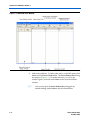
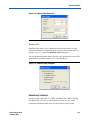
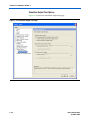
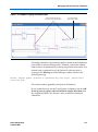
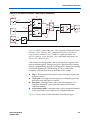
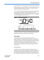
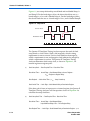
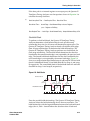
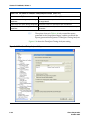
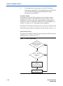
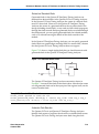
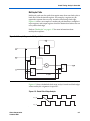
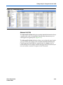
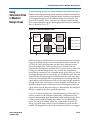
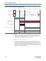
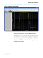
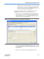
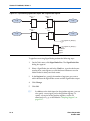
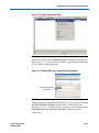
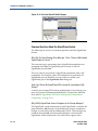
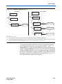
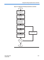
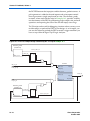
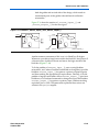
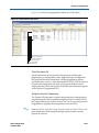
1
Quartus II Version 7.2 Handbook
Volume 3: Verification
Preliminary Information
101 Innovation Drive
San Jose, CA 95134
www.altera.com
QII5V3-7.2
Copyright © 2007 Altera Corporation. All rights reserved. Altera, The Programmable Solutions Company, the stylized Altera logo, specific device designations, and all other words and logos that are identified as trademarks and/or service marks are, unless noted otherwise, the trademarks and
service marks of Altera Corporation in the U.S. and other countries. All other product or service names are the property of their respective holders. Altera products are protected under numerous U.S. and foreign patents and pending applications, maskwork rights, and copyrights. Altera warrants
performance of its semiconductor products to current specifications in accordance with Altera's standard warranty, but reserves the right to make
changes to any products and services at any time without notice. Altera assumes no responsibility or liability arising out of the application or use of any information, product, or service described herein except as expressly agreed to in writing by Altera
Corporation. Altera customers are advised to obtain the latest version of device specifications before relying on any published information and before placing orders for products or services.
ii
Preliminary
Altera Corporation
Contents
Chapter Revision Dates ........................................................................ xxix
About this Handbook ............................................................................ xxxi
How to Contact Altera ........................................................................................................................ xxxi
Third-Party Software Product Information ..................................................................................... xxxi
Typographic Conventions ................................................................................................................. xxxii
Section I. Simulation
Chapter 1. Quartus II Simulator
Introduction ............................................................................................................................................ 1–1
Simulation Flow ..................................................................................................................................... 1–1
Functional Simulation ...................................................................................................................... 1–3
Timing Simulation ............................................................................................................................ 1–4
Timing Simulation Using Fast Timing Model Simulation ......................................................... 1–4
Waveform Editor ................................................................................................................................... 1–5
Creating VWFs .................................................................................................................................. 1–5
Count Value ............................................................................................................................... 1–11
Clock ........................................................................................................................................... 1–11
Arbitrary Value ......................................................................................................................... 1–12
Random Value ........................................................................................................................... 1–13
Generating a Testbench ................................................................................................................. 1–13
Grid Size .......................................................................................................................................... 1–14
Time Bars ......................................................................................................................................... 1–14
Stretch or Compress a Waveform Interval ................................................................................. 1–15
End Time .......................................................................................................................................... 1–16
Arrange Group or Bus in LSB or MSB Order ............................................................................. 1–17
Simulator Settings ................................................................................................................................ 1–17
Simulation Verification Options .................................................................................................. 1–21
Simulation Output Files Options ................................................................................................. 1–24
Simulation Report ................................................................................................................................ 1–25
Simulation Waveform .................................................................................................................... 1–25
Simulating Bidirectional Pin ......................................................................................................... 1–26
Logical Memories Report .............................................................................................................. 1–27
Simulation Coverage Reports ....................................................................................................... 1–27
Comparing Two Waveforms ........................................................................................................ 1–28
Debugging with the Quartus II Simulator ....................................................................................... 1–29
Breakpoints ...................................................................................................................................... 1–29
Updating Memory Content .......................................................................................................... 1–30
Altera Corporation
iii
Preliminary
Quartus II Handbook, Volume 3
Last Simulation Vector Outputs ...................................................................................................
Conventional Debugging Process ................................................................................................
Accessing Internal Signals for Simulation .............................................................................
Scripting Support .................................................................................................................................
Conclusion ............................................................................................................................................
Referenced Documents .......................................................................................................................
Document Revision History ...............................................................................................................
1–30
1–30
1–30
1–32
1–33
1–33
1–34
Chapter 2. Mentor Graphics ModelSim Support
Introduction ............................................................................................................................................ 2–1
Background ............................................................................................................................................. 2–1
Software Compatibility ......................................................................................................................... 2–3
Altera Design Flow with ModelSim or ModelSim-Altera Software .............................................. 2–3
Functional RTL Simulation .................................................................................................................. 2–5
Functional Simulation Libraries ..................................................................................................... 2–5
lpm Simulation Models .............................................................................................................. 2–5
Altera Megafunction Simulation Models ................................................................................ 2–6
Low-Level Primitive Simulation Models ................................................................................ 2–7
Simulating VHDL Designs .............................................................................................................. 2–7
Create Simulation Libraries ....................................................................................................... 2–7
Create Simulation Libraries Using the ModelSim GUI .................................................... 2–8
Create Simulation Libraries Using the ModelSim Command Prompt .......................... 2–8
Compile Simulation Models into Simulation Libraries ......................................................... 2–8
Compile Simulation Models into Simulation Libraries Using the ModelSim GUI ..... 2–8
Compile Simulation Models into Simulation Libraries at the ModelSim Command
Prompt ..................................................................................................................................... 2–9
Compile Testbench and Design Files into Work Library ...................................................... 2–9
Compile Testbench and Design Files into Work Library Using the ModelSim Command
Prompt ..................................................................................................................................... 2–9
Loading the Design ..................................................................................................................... 2–9
Loading the Design Using the ModelSim Command Prompt ...................................... 2–10
Running the Simulation ........................................................................................................... 2–10
Running the Simulation Using the ModelSim Command Prompt .............................. 2–10
Simulating Verilog HDL Designs ................................................................................................ 2–10
Create Simulation Libraries ..................................................................................................... 2–10
Create Simulation Libraries Using the ModelSim GUI .................................................. 2–11
Create Simulation Libraries Using the ModelSim Command Prompt ........................ 2–11
Compile Simulation Models into Simulation Libraries ....................................................... 2–11
Compile Simulation Models into Simulation Libraries Using the ModelSim GUI ... 2–11
Compile Simulation Models into Simulation Libraries Using the ModelSim Command
Prompt ................................................................................................................................... 2–12
Compile Testbench and Design Files into Work Library .................................................... 2–12
Compile Testbench and Design Files into Work Library Using the ModelSim Command
Prompt ................................................................................................................................... 2–12
iv
Preliminary
Altera Corporation
Contents
Loading the Design ................................................................................................................... 2–12
Loading a Design Using the ModelSim Command Prompt ......................................... 2–13
Running the Simulation ........................................................................................................... 2–13
Running the Simulation Using the ModelSim Command Prompt .............................. 2–13
Verilog HDL Functional RTL Simulation with Altera Memory Blocks ............................ 2–13
Post-Synthesis Simulation .................................................................................................................. 2–16
Generating a Post-Synthesis Simulation Netlist ........................................................................ 2–16
Simulating VHDL Designs ............................................................................................................ 2–17
Create Simulation Libraries ..................................................................................................... 2–17
Create Simulation Libraries Using the ModelSim GUI .................................................. 2–17
Create Simulation Libraries Using the ModelSim Command Prompt ........................ 2–18
Compile Simulation Models into Simulation Libraries Using the ModelSim GUI ... 2–18
Compile Simulation Models into Simulation Libraries Using the ModelSim Command
Prompt ................................................................................................................................... 2–18
Compile Testbench and VHDL Output File into Work Library ........................................ 2–18
Compile Testbench and VHDL Output File into Work Library Using ModelSim
Command Prompt ............................................................................................................... 2–19
Loading the Design ................................................................................................................... 2–19
Loading the Design Using the ModelSim Command Prompt ...................................... 2–19
Running the Simulation ........................................................................................................... 2–19
Running the Simulation Using the ModelSim Command Prompt .............................. 2–20
Simulating Verilog HDL Designs ................................................................................................ 2–20
Create Simulation Libraries ..................................................................................................... 2–20
Create Simulation Libraries Using the ModelSim GUI .................................................. 2–20
Create Simulation Libraries Using the ModelSim Command Prompt ........................ 2–20
Compile Simulation Models into Simulation Libraries Using the ModelSim GUI ... 2–21
Compile Simulation Models into Simulation Libraries Using the ModelSim Command
Prompt ................................................................................................................................... 2–21
Compile Testbench and Verilog Output File into Work Library ....................................... 2–21
Compile Testbench and Verilog Output File into Work Library Using the ModelSim
Command Prompt ............................................................................................................... 2–21
Loading the Design ................................................................................................................... 2–22
Loading the Design Using the ModelSim Command Prompt ...................................... 2–22
Running the Simulation ........................................................................................................... 2–22
Running the Simulation Using the ModelSim Command Prompt .............................. 2–23
Gate-Level Timing Simulation ........................................................................................................... 2–23
Generating a Gate-Level Timing Simulation Netlist ................................................................. 2–23
Generating a Different Timing Model ................................................................................... 2–24
Operating Condition Example: Generate All Timing Models for Stratix III Devices 2–25
Perform Timing Simulation Using Post-synthesis Netlist .................................................. 2–26
Gate-Level Simulation Libraries .................................................................................................. 2–27
Simulating VHDL Designs ............................................................................................................ 2–29
Create Simulation Libraries ..................................................................................................... 2–30
Create Simulation Libraries Using the ModelSim GUI .................................................. 2–30
Create Simulation Libraries Using the ModelSim Command Prompt ........................ 2–31
Compile Simulation Models into Simulation Libraries Using the ModelSim GUI ... 2–31
Compile Simulation Models into Simulation Libraries Using the ModelSim Command
Prompt ................................................................................................................................... 2–31
Altera Corporation
v
Preliminary
Quartus II Handbook, Volume 3
Compile Testbench and VHDL Output File into Work Library ........................................ 2–31
Compile Testbench and VHDL Output File into Work Library Using the ModelSim
Command Prompt ............................................................................................................... 2–32
Loading the Design ................................................................................................................... 2–32
Loading a Design Using the ModelSim Command Prompt ......................................... 2–33
Running the Simulation ........................................................................................................... 2–33
Running a Simulation Using the ModelSim Command Prompt .................................. 2–33
Simulating Verilog HDL Designs ................................................................................................ 2–33
Create Simulation Libraries ..................................................................................................... 2–33
Create Simulation Libraries Using the ModelSim GUI .................................................. 2–34
Create Simulation Libraries Using the ModelSim Command Prompt ........................ 2–34
Compile Simulation Models into Simulation Libraries Using the ModelSim GUI ... 2–34
Compile Simulation Models into Simulation Libraries Using the ModelSim Command
Prompt ................................................................................................................................... 2–35
Compile Testbench and Verilog Output File into Work Library ....................................... 2–35
Compile Testbench and Verilog Output File into Work Libraries Using the ModelSim
Command Prompt ............................................................................................................... 2–35
Loading the Design ................................................................................................................... 2–35
Loading the Design Using the ModelSim Command Prompt ...................................... 2–36
Running the Simulation ........................................................................................................... 2–36
Running the Simulation Using the ModelSim Command Prompt .............................. 2–36
Simulating Designs that Include Transceivers ................................................................................ 2–37
Stratix GX Functional Simulation ................................................................................................ 2–37
Example: Performing Functional Simulation for Stratix GX in Verilog HDL .................. 2–37
Example: Performing Functional Simulation for Stratix GX in VHDL ............................. 2–37
Stratix GX Post-Fit (Timing) Simulation ..................................................................................... 2–38
Example: Performing Timing Simulation for Stratix GX in Verilog HDL ........................ 2–38
Example: Performing Timing Simulation for Stratix GX in VHDL ................................... 2–39
Stratix II GX Functional Simulation ............................................................................................. 2–39
Example: Performing Functional Simulation for Stratix II GX in Verilog HDL .............. 2–40
Example: Performing Functional Simulation for Stratix II GX in VHDL ......................... 2–41
Stratix II GX Post-Fit (Timing) Simulation ................................................................................. 2–41
Example: Performing Timing Simulation for Stratix II GX in Verilog HDL .................... 2–42
Example: Performing Timing Simulation for Stratix II GX in VHDL ............................... 2–42
Transport Delays ............................................................................................................................ 2–43
+transport_path_delays ........................................................................................................... 2–43
+transport_int_delays .............................................................................................................. 2–43
Using the NativeLink Feature with ModelSim ............................................................................... 2–44
Setting Up NativeLink ................................................................................................................... 2–44
Performing an RTL Simulation Using NativeLink .................................................................... 2–44
Performing a Gate-Level Simulation Using NativeLink .......................................................... 2–47
Setting Up a Testbench .................................................................................................................. 2–48
Creating a Testbench ................................................................................................................ 2–49
Scripting Support ................................................................................................................................. 2–50
Generating a Post-Synthesis Simulation Netlist for ModelSim ............................................... 2–50
Tcl Commands ........................................................................................................................... 2–50
Command Prompt .................................................................................................................... 2–50
Generating a Gate-Level Timing Simulation Netlist for ModelSim ....................................... 2–51
Tcl Commands ........................................................................................................................... 2–51
vi
Preliminary
Altera Corporation
Contents
Command Line ..........................................................................................................................
Software Licensing and Licensing Setup .........................................................................................
LM_LICENSE_FILE Variable .......................................................................................................
Conclusion ............................................................................................................................................
Referenced Documents .......................................................................................................................
Document Revision History ...............................................................................................................
2–51
2–51
2–52
2–52
2–52
2–53
Chapter 3. Synopsys VCS Support
Introduction ............................................................................................................................................ 3–1
Software Requirements ......................................................................................................................... 3–1
Using VCS in the Quartus II Design Flow ......................................................................................... 3–3
Using VCS in the Quartus II Design Flow ...........................................................................................3–3
Functional Simulations .................................................................................................................... 3–4
Megafunctions Requiring Atom Libraries .............................................................................. 3–5
Functional RTL Simulation with Altera Memory Blocks ...................................................... 3–5
Compiling Functional Library Files with Compiler Directives ...................................... 3–5
Post-Synthesis Simulation ............................................................................................................... 3–6
Generating a Post-Synthesis Simulation Netlist ..................................................................... 3–6
Gate-Level Timing Simulation ....................................................................................................... 3–8
Generating a Gate-Level Timing Simulation Netlist ................................................................... 3–8
Generating Different Timing Model ........................................................................................ 3–9
Operating Condition Example: Generate All Timing Models for Stratix III Devices 3–10
Perform Timing Simulation Using Post-Synthesis Netlist ....................................................... 3–11
Common VCS Software Compiler Options ..................................................................................... 3–11
Using VirSim ........................................................................................................................................ 3–12
Debugging Support Command-Line Interface ............................................................................... 3–12
Simulating Designs that Include Transceivers ................................................................................ 3–13
Stratix GX Functional Simulation ................................................................................................ 3–13
Example of Compiling Library Files for Functional Stratix GX Simulation in Verilog HDL .
........................................................................................................................................................3–13
Stratix GX Post-Fit (Timing) Simulation ..................................................................................... 3–13
Example of Compiling Library Files for Timing Stratix GX Simulation in Verilog HDL .......
........................................................................................................................................................3–14
Stratix II GX Functional Simulation ............................................................................................. 3–14
Example of Compiling Library Files for Functional Stratix II GX Simulation in Verilog HDL
......................................................................................................................................................3–15
Stratix II GX Post-Fit (Timing) Simulation ................................................................................. 3–16
Example of Compiling Library Files for Timing Stratix II GX Simulation in Verilog HDL ...
........................................................................................................................................................3–16
Using PLI Routines with the VCS Software .................................................................................... 3–16
Preparing and Linking C Programs to Verilog HDL Code ...................................................... 3–16
Transport Delays .................................................................................................................................. 3–17
+transport_path_delays ........................................................................................................... 3–17
+transport_int_delays .............................................................................................................. 3–17
Using NativeLink with the VCS Software ....................................................................................... 3–18
Setting Up NativeLink ................................................................................................................... 3–18
Performing an RTL Simulation Using NativeLink .................................................................... 3–18
Altera Corporation
vii
Preliminary
Quartus II Handbook, Volume 3
Performing a Gate-Level Simulation Using NativeLink ..........................................................
Setting Up a Testbench ..................................................................................................................
Creating a Testbench ................................................................................................................
Scripting Support .................................................................................................................................
Generating a Post-Synthesis Simulation Netlist for VCS .........................................................
Tcl Commands ...........................................................................................................................
Command Prompt ....................................................................................................................
Generating a Gate-Level Timing Simulation Netlist for VCS ..................................................
Tcl Commands ...........................................................................................................................
Command Prompt ....................................................................................................................
Conclusion ............................................................................................................................................
Referenced Documents .......................................................................................................................
Document Revision History ...............................................................................................................
3–20
3–21
3–22
3–23
3–23
3–23
3–23
3–23
3–24
3–24
3–24
3–24
3–25
Chapter 4. Cadence NC-Sim Support
Introduction ............................................................................................................................................ 4–1
Software Requirements ......................................................................................................................... 4–1
Simulation Flow Overview ....................................................................................................................4–3
Operation Modes .............................................................................................................................. 4–4
Quartus II Software and NC Simulation Flow Overview .......................................................... 4–5
Functional and RTL Simulation ........................................................................................................... 4–6
Create Libraries ................................................................................................................................ 4–6
Basic Library Setup ..................................................................................................................... 4–7
Using Multiple cds.lib Files .................................................................................................. 4–7
Create a cds.lib File in Command-Line Mode ................................................................... 4–8
Create a cds.lib File in GUI Mode ....................................................................................... 4–8
LPM Functions, Altera Megafunctions, and Altera Primitives Libraries ........................... 4–9
Megafunctions Requiring Atom Libraries ............................................................................ 4–11
Simulating a Design with Memory .............................................................................................. 4–11
Compile Source Code and Testbenches ...................................................................................... 4–13
Compilation in Command-Line Mode .................................................................................. 4–13
Compilation in GUI Mode ....................................................................................................... 4–14
Elaborate Your Design ................................................................................................................... 4–15
Elaboration in Command-Line Mode .................................................................................... 4–15
Elaboration in GUI Mode ......................................................................................................... 4–16
Add Signals to View ...................................................................................................................... 4–17
Adding Signals in Command-Line Mode ............................................................................. 4–17
Adding Signals in GUI Mode .................................................................................................. 4–18
Simulate Your Design .................................................................................................................... 4–20
Functional/RTL Simulation in Command-Line Mode ....................................................... 4–21
Functional/RTL Simulation in GUI Mode ............................................................................ 4–21
Post-Synthesis Simulation .................................................................................................................. 4–22
Quartus II Simulation Output Files ............................................................................................. 4–22
Create Libraries .............................................................................................................................. 4–23
viii
Preliminary
Altera Corporation
Contents
Compile Project Files and Libraries ............................................................................................. 4–23
Elaborate Your Design ................................................................................................................... 4–23
Add Signals to the View ................................................................................................................ 4–23
Simulate Your Design .................................................................................................................... 4–24
Gate-Level Timing Simulation ........................................................................................................... 4–24
Generating a Gate-Level Timing Simulation Netlist ................................................................. 4–24
Generating a Different Timing Model ................................................................................... 4–25
Operating Condition Example: Generate All Timing Models for Stratix III and
Cyclone III Devices .............................................................................................................. 4–26
Perform Timing Simulation Using Post-Synthesis Netlist ....................................................... 4–27
Quartus II Timing Simulation Libraries ...................................................................................... 4–27
Create Libraries .............................................................................................................................. 4–28
Compile the Project Files and Libraries ...................................................................................... 4–28
Elaborate Your Design ................................................................................................................... 4–28
Compiling the Standard Delay Output File (VHDL Only)
in Command-Line Mode .......................................................................................................... 4–29
Compiling the Standard Delay Output File (VHDL Only) in GUI Mode ........................ 4–30
Add Signals to View ...................................................................................................................... 4–30
Simulate Your Design .................................................................................................................... 4–31
Simulating Designs that Include Transceivers ................................................................................ 4–31
Stratix GX Functional Simulation ................................................................................................ 4–31
Example of Compiling Library Files for Functional Stratix GX Simulation in Verilog HDL .
........................................................................................................................................................4–31
Example of Compiling Library Files for Functional Stratix GX Simulation in VHDL ... 4–31
Stratix GX Post-Fit (Timing) Simulation ..................................................................................... 4–32
Example of Compiling Library Files for Timing Stratix GX Simulation in Verilog HDL .......
.............................................................................................................................. .........................4–32
Example of Compiling Library Files for Timing Stratix GX Simulation in VHDL ......... 4–32
Stratix II GX Functional Simulation ............................................................................................. 4–33
Example of Compiling Library Files for Functional Stratix II GX Simulation in Verilog HDL
......................................................................................................................................................4–34
Example of Compiling Library Files for Functional Stratix II GX Simulation in VHDL 4–35
Stratix II GX Post-Fit (Timing) Simulation ................................................................................. 4–35
Example of Compiling Library Files for Timing Stratix II GX Simulation in Verilog HDL ...
......................................................................................................................................... ..............4–35
Example of Compiling Library Files for Timing Stratix II GX Simulation in VHDL ...... 4–36
Pulse Reject Delays ......................................................................................................................... 4–36
-PULSE_R ................................................................................................................................... 4–36
-PULSE_INT_R .......................................................................................................................... 4–36
Using the NativeLink Feature with NC-Sim ................................................................................... 4–37
Setting Up NativeLink ................................................................................................................... 4–37
Performing an RTL Simulation Using NativeLink .................................................................... 4–37
Performing a Gate Level Simulation Using NativeLink ........................................................... 4–40
Setting Up a Testbench .................................................................................................................. 4–40
Creating a Testbench ................................................................................................................ 4–42
Incorporating PLI Routines ................................................................................................................ 4–43
Dynamically Link a PLI Library ................................................................................................... 4–43
Altera Corporation
ix
Preliminary
Quartus II Handbook, Volume 3
Dynamically Load a PLI Library ..................................................................................................
Statically Link the PLI Library with NC-Sim .............................................................................
Scripting Support .................................................................................................................................
Generate NC-Sim Simulation Output Files ................................................................................
Tcl Commands: ..........................................................................................................................
Command Prompt ....................................................................................................................
Conclusion ............................................................................................................................................
Referenced Documents .......................................................................................................................
Document Revision History ...............................................................................................................
4–44
4–47
4–48
4–49
4–49
4–49
4–49
4–50
4–50
Chapter 5. Simulating Altera IP in Third-Party Simulation Tools
Introduction ............................................................................................................................................ 5–1
IP Functional Simulation Flow ............................................................................................................ 5–1
Verilog and VHDL IP Functional Simulation (IPFS) Models .................................................... 5–2
Instantiate the IP in Your Design ........................................................................................................ 5–3
Perform Simulation ............................................................................................................................... 5–4
Simulating Altera IP Using the Quartus II NativeLink Feature ................................................ 5–4
Set up a Quartus II Project ......................................................................................................... 5–5
Select the Third-Party Simulation Tool .................................................................................... 5–5
Specify the Path for the Third-Party Simulator ...................................................................... 5–7
Specify the Testbench Settings .................................................................................................. 5–7
Analyze and Elaborate the Quartus II Project ........................................................................ 5–9
Run RTL Functional Simulation ............................................................................................... 5–9
Simulating Altera IP Without the Quartus II NativeLink Feature ............................................ 5–9
Design Language Examples ....................... .........................................................................................5–11
Verilog HDL Example: Simulating the IPFS Model in the ModelSim Software ................... 5–11
VHDL Example: Simulating the IPFS Model in the ModelSim Software .............................. 5–12
NC-VHDL Example: Simulating the IPFS Model in the NC-VHDL Software ..................... 5–14
Verilog HDL Example: Simulating Your IPFS Model in VCS ................................................. 5–15
Single-Step Process ................................................................................................................... 5–15
Two-Step Process (Compilation and Simulation) ................................................................ 5–16
Conclusion ............................................................................................................................................ 5–16
Referenced Documents ....................................................................................................................... 5–16
Document Revision History ............................................................................................................... 5–17
Section II. Timing Analysis
Chapter 6. The Quartus II TimeQuest Timing Analyzer
Introduction ............................................................................................................................................
Getting Started with the Quartus II TimeQuest Timing Analyzer .................................................
Setting Up the Quartus II TimeQuest Timing Analyzer ............................................................
Compilation Flow with the Quartus II TimeQuest Timing Analyzer Guidelines .......................
Running the Quartus II TimeQuest Timing Analyzer ................................................................
Directly from the Quartus II Software .....................................................................................
Stand-Alone Mode ......................................................................................................................
x
Preliminary
6–1
6–2
6–2
6–3
6–4
6–4
6–5
Altera Corporation
Contents
Command-Line Mode ................................................................................................................ 6–5
Timing Analysis Overview .................................................................................................................. 6–7
Clock Analysis ................................................................................................................................ 6–11
Clock Setup Check .................................................................................................................... 6–11
Clock Hold Check ..................................................................................................................... 6–13
Recovery and Removal ............................................................................................................ 6–15
Multicycle Paths ........................................................................................................................ 6–16
Specify Design Timing Requirements .............................................................................................. 6–19
Create a Timing Netlist ................................................................................................................. 6–19
Specify Timing Constraints ........................................................................................................... 6–20
Generate SDC Constraint Reports ............................................................................................... 6–21
The Quartus II TimeQuest Timing Analyzer Flow Guidelines .................................................... 6–22
Create a Timing Netlist ................................................................................................................. 6–22
Read the Synopsys Design Constraints File ............................................................................... 6–22
Update Timing Netlist ................................................................................................................... 6–23
Generate Timing Reports .............................................................................................................. 6–23
Collections ............................................................................................................................................ 6–23
Application Examples .............................................................................................................. 6–25
Constraints Files ................................................................................................................................... 6–25
Fitter and Timing Analysis SDC Files ......................................................................................... 6–26
Specifying SDC Files for Place-and-Route ............................................................................ 6–26
Specifying SDC Files for Static Timing Analysis .................................................................. 6–26
Synopsys Design Constraints File Precedence ........................................................................... 6–27
Clock Specification .............................................................................................................................. 6–28
Clocks ............................................................................................................................................... 6–28
Generated Clocks ........................................................................................................................... 6–29
Virtual Clocks ................................................................................................................................. 6–32
Multi-Frequency Clocks ................................................................................................................ 6–33
Automatic Clock Detection ........................................................................................................... 6–34
Derive PLL Clocks .......................................................................................................................... 6–35
Default Clock Constraints ............................................................................................................. 6–37
Clock Groups .................................................................................................................................. 6–37
Clock Effect Characteristics .......................................................................................................... 6–39
Clock Latency ............................................................................................................................ 6–39
Clock Uncertainty ..................................................................................................................... 6–40
Derive Clock Uncertainty .............................................................................................................. 6–41
Inter-Clock Transfers ................................................................................................................ 6–42
Intra-Clock Transfers ................................................................................................................ 6–43
I/O Interface Clock Transfers ................................................................................................. 6–43
I/O Specifications ................................................................................................................................ 6–45
Input and Output Delay ................................................................................................................ 6–45
Set Input Delay .......................................................................................................................... 6–45
Set Output Delay ....................................................................................................................... 6–47
Timing Exceptions ............................................................................................................................... 6–48
Precedence ....................................................................................................................................... 6–49
False Path ......................................................................................................................................... 6–49
Minimum Delay ............................................................................................................................. 6–50
Altera Corporation
xi
Preliminary
Quartus II Handbook, Volume 3
Maximum Delay ............................................................................................................................. 6–52
Multicycle Path ............................................................................................................................... 6–53
Clock-as-Data Analysis ................................................................................................................. 6–55
Application Examples .................................................................................................................... 6–55
Constraint and Exception Removal .................................................................................................. 6–57
Timing Reports ..................................................................................................................................... 6–58
report_timing .................................................................................................................................. 6–58
report_clock_transfers ................................................................................................................... 6–62
report_clocks ................................................................................................................................... 6–63
report_min_pulse_width ............................................................................................................... 6–63
report_net_timing ........................................................................................................................... 6–65
report_sdc ........................................................................................................................................ 6–66
report_ucp ....................................................................................................................................... 6–66
report_path ...................................................................................................................................... 6–68
report_datasheet ............................................................................................................................. 6–69
report_rskm ..................................................................................................................................... 6–70
report_tccs ....................................................................................................................................... 6–70
report_path ...................................................................................................................................... 6–71
check_timing ................................................................................................................................... 6–73
report_clock_fmax_summary ....................................................................................................... 6–75
create_timing_summary ................................................................................................................ 6–76
Timing Analysis Features ................................................................................................................... 6–77
Multi-Corner Analysis ................................................................................................................... 6–77
Advanced I/O Timing and Board Trace Model Assignments ................................................ 6–79
Wildcard Assignments and Collections ...................................................................................... 6–79
Resetting a Design .......................................................................................................................... 6–81
The TimeQuest Timing Analyzer GUI ............................................................................................. 6–82
The Quartus II Software Interface and Options ......................................................................... 6–83
View Pane ........................................................................................................................................ 6–85
View Pane: Splitting ................................................................................................................. 6–85
View Pane: Removing Split Windows ................................................................................... 6–86
Tasks Pane ....................................................................................................................................... 6–87
Opening a Project and Writing a Synopsys Design Constraints File ................................ 6–87
Netlist Setup Folder .................................................................................................................. 6–88
Reports Folder ........................................................................................................................... 6–88
Macros Folder ............................................................................................................................ 6–89
Console Pane ................................................................................................................................... 6–90
Report Pane ..................................................................................................................................... 6–90
Constraints ...................................................................................................................................... 6–90
Name Finder ................................................................................................................................... 6–92
Target Pane ...................................................................................................................................... 6–94
SDC Editor ....................................................................................................................................... 6–94
Conclusion ............................................................................................................................................ 6–95
Referenced Documents ....................................................................................................................... 6–95
Document Revision History ............................................................................................................... 6–96
xii
Preliminary
Altera Corporation
Contents
Chapter 7. Switching to the Quartus II TimeQuest Timing Analyzer
Introduction ............................................................................................................................................ 7–1
Benefits of Switching to the Quartus II TimeQuest Analyzer ................................................... 7–1
Chapter Contents .............................................................................................................................. 7–2
Switching to the Quartus II TimeQuest Analyzer ............................................................................ 7–2
Compile Your Design ...................................................................................................................... 7–2
Create an SDC File ........................................................................................................................... 7–3
Conversion Utility ....................................................................................................................... 7–3
Perform Timing Analysis with the Quartus II TimeQuest Timing Analyzer ......................... 7–4
Run the Quartus II TimeQuest Analyzer ................................................................................ 7–4
Set the Default Timing Analyzer .................................................................................................... 7–4
Differences Between Quartus II TimeQuest and Quartus II Classic Timing Analyzers ............. 7–5
Terminology ...................................................................................................................................... 7–5
Netlist ............................................................................................................................................ 7–6
Collections .................................................................................................................................... 7–7
Constraints ........................................................................................................................................ 7–7
Constraint Files ............................................................................................................................ 7–7
Constraint Entry .......................................................................................................................... 7–8
Time Units .............................................................................................................................. 7–9
MegaCore Functions ............................................................................................................. 7–9
Bus Name Format ................................................................................................................ 7–10
Constraint File Priority ............................................................................................................. 7–10
Constraint Priority .................................................................................................................... 7–11
Ambiguous Constraints ........................................................................................................... 7–12
Clocks ............................................................................................................................................... 7–13
Related and Unrelated Clocks ................................................................................................. 7–13
Clock Offset ................................................................................................................................ 7–14
Clock Latency ............................................................................................................................ 7–15
Offset and Latency Example ................................................................................................... 7–15
Clock Offset Scenario .......................................................................................................... 7–16
Clock Latency Scenario ....................................................................................................... 7–17
Clock Uncertainty ..................................................................................................................... 7–18
Derived and Generated Clocks ............................................................................................... 7–19
Automatic Clock Detection ..................................................................................................... 7–19
derive_clocks Command .................................................................................................... 7–20
derive_pll_clocks Command ............................................................................................. 7–22
Hold Relationship ..................................................................................................................... 7–23
Clock Objects ................................................................................................................................... 7–23
Hold Multicycle .............................................................................................................................. 7–24
Fitter Behavior ................................................................................................................................ 7–27
Fitter Performance .................................................................................................................... 7–27
Reporting ......................................................................................................................................... 7–27
Paths and Pairs .......................................................................................................................... 7–28
Default Reports ......................................................................................................................... 7–28
Netlist Names ............................................................................................................................ 7–29
Non-Integer Clock Periods ...................................................................................................... 7–29
Other Features ........................................................................................................................... 7–30
Altera Corporation
xiii
Preliminary
Quartus II Handbook, Volume 3
Scripting API ................................................................................................................................... 7–32
Timing Assignment Conversion ....................................................................................................... 7–33
Setup Relationship ......................................................................................................................... 7–33
Hold Relationship .......................................................................................................................... 7–34
Clock Latency .................................................................................................................................. 7–34
Clock Uncertainty ........................................................................................................................... 7–34
Inverted Clock ................................................................................................................................. 7–35
Not a Clock ...................................................................................................................................... 7–35
Default Required fMAX Assignment ............................................................................................. 7–35
Virtual Clock Reference ................................................................................................................. 7–36
Clock Settings .................................................................................................................................. 7–37
Multicycle ........................................................................................................................................ 7–37
Clock Enable Multicycle ................................................................................................................ 7–38
I/O Constraints .............................................................................................................................. 7–38
Input and Output Delay ................................................................................................................ 7–39
tSU Requirement .............................................................................................................................. 7–40
tH Requirement ............................................................................................................................... 7–43
tCO Requirement ............................................................................................................................. 7–45
Minimum tCO Requirement .......................................................................................................... 7–48
tPD Requirement .............................................................................................................................. 7–50
Combinational Path Delay Scenario ................................................................................. 7–50
Minimum tPD Requirement ........................................................................................................... 7–51
Cut Timing Path ............................................................................................................................. 7–52
Maximum Delay ............................................................................................................................. 7–52
Minimum Delay ............................................................................................................................. 7–52
Maximum Clock Arrival Skew ..................................................................................................... 7–53
Maximum Data Arrival Skew ...................................................................................................... 7–53
Constraining Skew on an Output Bus .............................................................................. 7–53
Conversion Utility ............................................................................................................................... 7–55
Unsupported Global Assignments .............................................................................................. 7–56
Recommended Global Assignments ........................................................................................... 7–56
Clock Conversion ........................................................................................................................... 7–58
Instance Assignment Conversion ................................................................................................ 7–59
PLL Phase Shift Conversion .................................................................................................... 7–61
tCO Requirement Conversion ................................................................................................... 7–62
Entity-Specific Assignments ......................................................................................................... 7–63
Paths between Unrelated Clock Domains .................................................................................. 7–63
Unsupported Instance Assignments ........................................................................................... 7–64
Reviewing Conversion Results .................................................................................................... 7–64
Warning Messages .................................................................................................................... 7–64
Ignored QSF Variable <assignment> ................................................................................ 7–65
Global <name> = <value> .................................................................................................. 7–65
QSF: Expected <name> to be set to <expected value> but it is set to <actual value> .......
......................... .........................................................................................................................7–65
QSF: Found Global Fmax Requirement. Translation will be done using derive_clocks ....
............................. .....................................................................................................................7–65
TAN Report Database not found. HDL based assignments will not be migrated .... 7–65
xiv
Preliminary
Altera Corporation
Contents
Ignored Entity Assignment (Entity <entity>): <variable> = <value> -from <from> -to
<to> ........................................................................................................................................ 7–65
Ignoring OFFSET_FROM_BASE_CLOCK assignment for clock <clock> ................... 7–66
Clock <clock> has no FMAX_REQUIREMENT - No clock was generated ................ 7–66
No Clock Settings defined in QSF file .............................................................................. 7–66
Clocks .......................................................................................................................................... 7–66
Clock Transfers .......................................................................................................................... 7–66
Path Details ................................................................................................................................ 7–67
Unconstrained Paths ................................................................................................................. 7–67
Bus Names ................................................................................................................................. 7–68
Other ........................................................................................................................................... 7–68
Re-Running the Conversion Utility ............................................................................................. 7–68
Notes ...................................................................................................................................................... 7–68
Output Pin Load Assignments ..................................................................................................... 7–68
Constraint Target Types ................................................................................................................ 7–69
DDR Constraints with the DDR Timing Wizard ....................................................................... 7–69
HardCopy Stratix Device Handoff .............................................................................................. 7–69
Unsupported SDC Features .......................................................................................................... 7–69
Constraint Passing .......................................................................................................................... 7–70
Optimization ................................................................................................................................... 7–70
Clock Network Delay Reporting .................................................................................................. 7–70
PowerPlay Power Analysis ........................................................................................................... 7–70
Project Management ...................................................................................................................... 7–71
Conversion Utility .......................................................................................................................... 7–71
tPD and Minimum tPD Requirement Conversion .................................................................. 7–71
Referenced Documents ....................................................................................................................... 7–72
Document Revision History ............................................................................................................... 7–72
Chapter 8. Quartus II Classic Timing Analyzer
Introduction ............................................................................................................................................ 8–1
Timing Analysis Tool Setup ................................................................................................................. 8–2
Static Timing Analysis Overview ........................................................................................................ 8–2
Clock Analysis .................................................................................................................................. 8–4
Clock Setup Check ...................................................................................................................... 8–4
Clock Hold Check ....................................................................................................................... 8–6
Multicycle Paths ............................................................................................................................... 8–7
Clock Settings ......................................................................................................................................... 8–8
Individual Clock Settings ................................................................................................................ 8–8
Default Clock Settings ..................................................................................................................... 8–8
Clock Types ............................................................................................................................................ 8–9
Base Clocks ........................................................................................................................................ 8–9
Derived Clocks .................................................................................................................................. 8–9
Undefined Clocks ............................................................................................................................. 8–9
PLL Clocks ....................................................................................................................................... 8–10
Clock Uncertainty ................................................................................................................................ 8–11
Clock Latency ....................................................................................................................................... 8–12
Timing Exceptions ............................................................................................................................... 8–15
Altera Corporation
xv
Preliminary
Quartus II Handbook, Volume 3
Multicycle ........................................................................................................................................
Destination Multicycle Setup Exception ................................................................................
Destination Multicycle Hold Exception .................................................................................
Source Multicycle Setup Exception ........................................................................................
Source Multicycle Hold Exception .........................................................................................
Default Hold Multicycle ..........................................................................................................
Clock Enable Multicycle ...........................................................................................................
Setup Relationship and Hold Relationship ................................................................................
Maximum Delay and Minimum Delay .......................................................................................
False Paths .......................................................................................................................................
I/O Analysis .........................................................................................................................................
External Input Delay and Output Delay Assignments .............................................................
Input Delay Assignment ..........................................................................................................
Output Delay Assignment .......................................................................................................
Virtual Clocks .................................................................................................................................
Asynchronous Paths ............................................................................................................................
Recovery and Removal ..................................................................................................................
Recovery Report ........................................................................................................................
Removal Report .........................................................................................................................
Skew Management ..............................................................................................................................
Maximum Clock Arrival Skew .....................................................................................................
Maximum Data Arrival Skew ......................................................................................................
Generating Timing Analysis Reports with report_timing ............................................................
Other Timing Analyzer Features .......................................................................................................
Wildcard Assignments ..................................................................................................................
Assignment Groups .......................................................................................................................
Fast Corner Analysis ......................................................................................................................
Early Timing Estimation ...............................................................................................................
Timing Constraint Checker ...........................................................................................................
Latch Analysis .................................................................................................................................
Timing Analysis Using the Quartus II GUI .....................................................................................
Assignment Editor .........................................................................................................................
Timing Settings ...............................................................................................................................
Clock Settings Dialog Box ........................................................................................................
More Timing Settings Dialog Box ...........................................................................................
Timing Reports ...............................................................................................................................
Advanced List Path ........................................................................................................................
Early Timing Estimate ...................................................................................................................
Assignment Groups .......................................................................................................................
Scripting Support .................................................................................................................................
Creating Clocks ...............................................................................................................................
Base Clocks .................................................................................................................................
Derived Clocks ..........................................................................................................................
Clock Latency ..................................................................................................................................
Clock Uncertainty ...........................................................................................................................
Cut Timing Paths ............................................................................................................................
Input Delay Assignment ...............................................................................................................
xvi
Preliminary
8–15
8–15
8–16
8–17
8–18
8–19
8–19
8–22
8–24
8–24
8–26
8–26
8–26
8–28
8–29
8–30
8–30
8–31
8–32
8–34
8–34
8–35
8–36
8–38
8–38
8–38
8–40
8–40
8–41
8–42
8–43
8–43
8–44
8–45
8–46
8–47
8–49
8–51
8–51
8–52
8–53
8–53
8–53
8–53
8–54
8–54
8–54
Altera Corporation
Contents
Maximum and Minimum Delay ..................................................................................................
Maximum Clock Arrival Skew .....................................................................................................
Maximum Data Arrival Skew ......................................................................................................
Multicycle ........................................................................................................................................
Output Delay Assignment ............................................................................................................
Report Timing .................................................................................................................................
Setup and Hold Relationships ......................................................................................................
Assignment Group .........................................................................................................................
Virtual Clock ...................................................................................................................................
MAX+PLUS II Timing Analysis Methodology ...............................................................................
fMAX Relationships ..........................................................................................................................
Slack ............................................................................................................................................
I/O Timing ......................................................................................................................................
tSU Timing ...................................................................................................................................
tH Timing ....................................................................................................................................
tCO Timing ..................................................................................................................................
Minimum tCO (min tCO) ............................................................................................................
tPD Timing ..................................................................................................................................
Minimum tPD (min tPD) .............................................................................................................
The Timing Analyzer Tool ............................................................................................................
Conclusion ............................................................................................................................................
Referenced Documents .......................................................................................................................
Document Revision History ...............................................................................................................
8–55
8–55
8–55
8–56
8–56
8–57
8–57
8–57
8–58
8–58
8–58
8–58
8–60
8–60
8–60
8–61
8–62
8–62
8–62
8–62
8–63
8–63
8–64
Chapter 9. Synopsys PrimeTime Support
Introduction ............................................................................................................................................ 9–1
Quartus II Settings for Generating the PrimeTime Software Files ................................................. 9–2
Files Generated for the PrimeTime Software Environment ............................................................ 9–3
The Netlist ......................................................................................................................................... 9–3
The SDO File ..................................................................................................................................... 9–4
Generating Multiple Operating Conditions with TimeQuest .............................................. 9–4
The Tcl Script .................................................................................................................................... 9–7
Generated File Summary ........................................................................................................... 9–9
Running the PrimeTime Software ..................................................................................................... 9–10
Analyzing Quartus II Projects ...................................................................................................... 9–10
Other pt_shell Commands ............................................................................................................ 9–11
PrimeTime Timing Reports ................................................................................................................ 9–12
Sample of the PrimeTime Software Timing Report .................................................................. 9–12
Comparing Timing Reports from the Quartus II Classic Timing Analyzer and the PrimeTime
Software ........................................................................................................................................... 9–13
Clock Setup Relationship and Slack ....................................................................................... 9–13
Clock Hold Relationship and Slack ........................................................................................ 9–17
Input Delay and Output Delay Relationships and Slack .................................................... 9–21
Static Timing Analyzer Differences .................................................................................................. 9–23
The Quartus II Classic Timing Analyzer and the PrimeTime Software ................................. 9–23
Rise/Fall Support ...................................................................................................................... 9–23
Minimum and Maximum Delays ........................................................................................... 9–23
Altera Corporation
xvii
Preliminary
Quartus II Handbook, Volume 3
Recovery/Removal Analysis ..................................................................................................
Encrypted Intellectual Property Blocks .................................................................................
Registered Clock Signals ..........................................................................................................
Multiple Source and Destination Register Pairs ...................................................................
Latches ........................................................................................................................................
LVDS I/O ...................................................................................................................................
Clock Latency ............................................................................................................................
Input and Output Delay Assignments ...................................................................................
Generated Clocks Derived from Generated Clocks .............................................................
The Quartus II TimeQuest Timing Analyzer and the PrimeTime Software .........................
Encrypted Intellectual Property Blocks .................................................................................
Latches ........................................................................................................................................
LVDS I/O ...................................................................................................................................
The Quartus II TimeQuest Timing Analyzer SDC File and PrimeTime Compatibility .
Clock and Data Paths ...............................................................................................................
Inverting and Non-Inverting Propagation ............................................................................
Multiple Rise/Fall Numbers For a Timing Arc ....................................................................
Virtual Generated Clocks .........................................................................................................
Generated Clocks Derived from Generated Clocks .............................................................
Conclusion ............................................................................................................................................
Referenced Documents .......................................................................................................................
Document Revision History ...............................................................................................................
9–23
9–24
9–24
9–25
9–25
9–25
9–26
9–26
9–26
9–26
9–26
9–27
9–27
9–27
9–27
9–28
9–28
9–28
9–28
9–28
9–29
9–30
Section III. Power Estimation and Analysis
Chapter 10. PowerPlay Power Analysis
Introduction .......................................................................................................................................... 10–1
Quartus II Early Power Estimator File ............................................................................................. 10–2
PowerPlay Early Power Estimator File Generator Compilation Report ................................ 10–5
Types of Power Analyses ................................................................................................................... 10–6
Factors Affecting Power Consumption ............................................................................................ 10–6
Device Selection .............................................................................................................................. 10–6
Environmental Conditions ............................................................................................................ 10–7
Air Flow ...................................................................................................................................... 10–7
Heat Sink and Thermal Compound ....................................................................................... 10–7
Ambient Temperature .............................................................................................................. 10–8
Board Thermal Model .............................................................................................................. 10–8
Design Resources ............................................................................................................................ 10–8
Number, Type, and Loading of I/O Pins .............................................................................. 10–8
Number and Type of Logic Elements, Multiplier Elements, and RAM Blocks ............... 10–8
Number and Type of Global Signals ...................................................................................... 10–9
Signal Activities .............................................................................................................................. 10–9
PowerPlay Power Analyzer Flow ............................. .......................................................................10–10
Operating Conditions .................................................................................................................. 10–11
Signal Activities Data Sources .................................................................................................... 10–12
xviii
Preliminary
Altera Corporation
Contents
Simulation Results .................................................................................................................. 10–13
Using Simulation Files in Modular Design Flows ........................... ..............................................10–15
Complete Design Simulation ...................................................................................................... 10–16
Modular Design Simulation ....................................................................................................... 10–16
Multiple Simulations on the Same Entity ................................................................................. 10–17
Overlapping Simulations ............................................................................................................ 10–18
Partial Simulations ....................................................................................................................... 10–18
Node Name Matching Considerations ..................................................................................... 10–18
Glitch Filtering .............................................................................................................................. 10–19
Node and Entity Assignments ................................................................................................... 10–21
Timing Assignments to Clock Nodes .................................................................................. 10–22
Default Toggle Rate Assignment ............................................................................................... 10–22
Vectorless Estimation ................................................................................................................... 10–23
Using the PowerPlay Power Analyzer ........................................................................................... 10–23
Common Analysis Flows ............................................................................................................ 10–23
Signal Activities from Full Post-Fit Netlist (Timing) Simulation ..................................... 10–23
Signal Activities from RTL (Functional) Simulation, Supplemented by Vectorless
Estimation ................................................................................................................................ 10–24
Signal Activities from Vectorless Estimation, User-Supplied Input Pin Activities ....... 10–24
Signal Activities from User Defaults Only .......................................................................... 10–24
Generating a SAF or VCD File Using the Quartus II Simulator ............................................ 10–24
Generating a VCD File Using a Third-Party Simulator .......................................................... 10–28
Running the PowerPlay Power Analyzer Using the Quartus II GUI ................................... 10–31
PowerPlay Power Analyzer Compilation Report ................................................................... 10–39
Summary .................................................................................................................................. 10–39
Settings ..................................................................................................................................... 10–39
Simulation Files Read ............................................................................................................. 10–39
Operating Conditions Used ................................................................................................... 10–39
Thermal Power Dissipated by Block .................................................................................... 10–39
Thermal Power Dissipation by Block Type (Device Resource Type) .............................. 10–39
Thermal Power Dissipation by Hierarchy ........................................................................... 10–40
Core Dynamic Thermal Power Dissipation by Clock Domain ........................................ 10–40
Current Drawn from Voltage Supplies ................................................................................ 10–40
Confidence Metric Details ..................................................................................................... 10–40
Signal Activities ....................................................................................................................... 10–41
Messages ................................................................................................................................... 10–41
Specific Rules for Reporting .................................................................................................. 10–41
Scripting Support ......................................................................................................................... 10–41
Running the PowerPlay Power Analyzer from the Command Line ............................... 10–42
Conclusion .......................................................................................................................................... 10–43
Referenced Documents ..................................................................................................................... 10–43
Document Revision History ............................................................................................................. 10–44
Altera Corporation
xix
Preliminary
Quartus II Handbook, Volume 3
Section IV. Signal Integrity
Chapter 11. Signal Integrity Analysis with Third-Party Tools
Introduction .......................................................................................................................................... 11–1
The Need for FPGA to Board Signal Integrity Analysis ................................................................ 11–3
The Double Counting Problem for FPGA Output Timing ............................................................ 11–4
Defining the Double Counting Problem ..................................................................................... 11–4
The Solution to Double Counting ................................................................................................ 11–5
I/O Model Selection: IBIS or HSPICE .............................................................................................. 11–7
FPGA to Board Signal Integrity Analysis Flow ............................................................................... 11–8
Create I/O and Board Trace Model Assignments ................................................................... 11–10
Enable Output File Generation ................................................................................................... 11–10
Generate the Output Files ........................................................................................................... 11–10
Customize the Output Files ........................................................................................................ 11–11
Set Up and Run Simulations in Third-Party Tools .................................................................. 11–11
Interpret Simulation Results ....................................................................................................... 11–12
Simulation with IBIS Models ........................................................................................................... 11–12
Elements of an IBIS Model .......................................................................................................... 11–12
Creating Accurate IBIS Models .................................................................................................. 11–13
Download IBIS Models .......................................................................................................... 11–13
Generate Custom IBIS Models with the IBIS Writer .......................................................... 11–14
Design Simulation Using the Mentor Graphics HyperLynx Software ................................. 11–17
Configuring LineSim to Use Altera IBIS Models ..................................................................... 11–20
Integrating Altera IBIS Models into LineSim Simulations ..................................................... 11–21
Running and Interpreting LineSim Simulations ..................................................................... 11–24
Simulation with HSPICE Models .................................................................................................... 11–25
Supported Devices and Signaling .............................................................................................. 11–26
Creating Accurate HSPICE Models ........................................................................................... 11–26
Creating HSPICE Model Files Using the Quartus II GUI ................................................. 11–27
Creating HSPICE Model Files Using Tcl Scripting and the Command Line ................. 11–28
Customizing HSPICE Model Files ............................................................................................. 11–29
Design Simulation Using Synopsys HSPICE ........................................................................... 11–30
Running HSPICE Simulations .................................................................................................... 11–30
Viewing and Interpreting Tabular Simulation Results ........................................................... 11–31
Viewing Graphical Simulation Results ..................................................................................... 11–31
Making Design Adjustments Based on HSPICE Simulations ............................................... 11–33
Conclusion .......................................................................................................................................... 11–35
Referenced Documents ..................................................................................................................... 11–36
Document Revision History ............................................................................................................. 11–36
Section V. In-System Design Debugging
Chapter 12. Quick Design Debugging Using SignalProbe
Introduction .......................................................................................................................................... 12–1
xx
Preliminary
Altera Corporation
Contents
On-Chip Debugging Tool Comparison ............................................................................................ 12–2
Debugging Using the SignalProbe Feature ...................................................................................... 12–4
Reserve the SignalProbe Pins ....................................................................................................... 12–4
Perform a Full Compilation .......................................................................................................... 12–6
Assign a SignalProbe Source ........................................................................................................ 12–6
Add Registers to the Pipeline Path to SignalProbe Pin ............................................................ 12–7
Perform a SignalProbe Compilation ............................................................................................ 12–9
Analyze the Results of the SignalProbe Compilation ............................................................. 12–10
Generate the Programming File ................................................................................................. 12–11
SignalProbe ECO flows ............................................................................................................... 12–11
SignalProbe ECO Flow with Quartus II Incremental Compilation ................................. 12–11
SignalProbe ECO Flow without Quartus Incremental Compilation ............................... 12–12
Common Questions About the SignalProbe Feature .............................................................. 12–14
Why Did I Get the Following Error Message, “Error: There are No Enabled SignalProbes to
Process”? .................................................................................................................................. 12–14
How Can I Retain My SignalProbe ECOs during Re-compilation of My Design? ....... 12–14
Why Did My SignalProbe Source Disappear in the Change Manager? ......................... 12–14
What is an ECO and Where Can I Find More Information on ECO? .............................. 12–15
How Do I Migrate My Previous SignalProbe Assignments in the Quartus II Software
Versions 5.1 and below to Versions 6.0 and Higher? ........................................................ 12–15
What are all the Changes for the SignalProbe Feature between the Quartus II Software
Version 5.1 and Earlier, and Version 6.0 and Later? .......................................................... 12–16
Scripting Support ......................................................................................................................... 12–17
Make a SignalProbe Pin ......................................................................................................... 12–17
Delete a SignalProbe Pin ........................................................................................................ 12–17
Enable a SignalProbe Pin ....................................................................................................... 12–18
Disable a SignalProbe Pin ...................................................................................................... 12–18
Perform a SignalProbe Compilation .................................................................................... 12–18
Migrating Previous SignalProbe Pins to the Quartus II Software Versions 6.0 and Later ......
.......................................... ...........................................................................................................12–18
Script Example ......................................................................................................................... 12–18
Using SignalProbe with the APEX Device Family ........................................................................ 12–19
Adding SignalProbe Sources ...................................................................................................... 12–19
Performing a SignalProbe Compilation .................................................................................... 12–20
Running SignalProbe with Smart Compilation .................................................................. 12–21
Understanding the Results of a SignalProbe Compilation .................................................... 12–21
Analyzing SignalProbe Routing Failures ............................................................................ 12–23
SignalProbe Scripting Support for APEX Devices ................................................................... 12–23
Reserving SignalProbe Pins ........................................................................................................ 12–24
Adding SignalProbe Sources ...................................................................................................... 12–24
Assigning I/O Standards ............................................................................................................ 12–24
Adding Registers for Pipelining ................................................................................................. 12–24
Run SignalProbe Automatically ................................................................................................. 12–25
Run SignalProbe Manually ......................................................................................................... 12–25
Enable or Disable All SignalProbe Routing .............................................................................. 12–25
Running SignalProbe with Smart Compilation ....................................................................... 12–26
Allow SignalProbe to Modify Fitting Results .......................................................................... 12–26
Altera Corporation
xxi
Preliminary
Quartus II Handbook, Volume 3
Conclusion .......................................................................................................................................... 12–26
Referenced Documents ..................................................................................................................... 12–26
Document Revision History ............................................................................................................. 12–27
Chapter 13. Design Debugging Using the SignalTap II Embedded Logic Analyzer
Introduction .......................................................................................................................................... 13–1
Hardware and Software Requirements ...................................................................................... 13–3
On-Chip Debugging Tool Comparison ............................................................................................ 13–5
Design Flow Using the SignalTap II Logic Analyzer ..................................................................... 13–7
SignalTap II Logic Analyzer Task Flow ........................................................................................... 13–8
Add the SignalTap II Logic Analyzer to Your Design .............................................................. 13–9
Configure the SignalTap II Logic Analyzer ................................................................................ 13–9
Define Triggers ............................................................................................................................... 13–9
Compile the Design ........................................................................................................................ 13–9
Program the Target Device or Devices ........................................................................................ 13–9
Run the SignalTap II Logic Analyzer ........................................................................................ 13–10
View, Analyze, and Use Captured Data ................................................................................... 13–10
Add the SignalTap II Logic Analyzer to Your Design ................................................................. 13–10
Creating and Enabling a SignalTap II File ................................................................................ 13–10
Creating a SignalTap II File ................................................................................................... 13–10
Enabling and Disabling a SignalTap II File for the Current Project ................................ 13–11
Using the MegaWizard Plug-In Manager to Create Your Embedded Logic Analyzer ..... 13–12
Creating an HDL Representation Using the MegaWizard Plug-In Manager ................ 13–12
SignalTap II Megafunction Ports .......................................................................................... 13–16
Instantiating the SignalTap II Logic Analyzer in Your HDL ............................................ 13–16
Embedding Multiple Analyzers in One FPGA ........................................................................ 13–17
Monitoring FPGA Resources Used by the SignalTap II Logic Analyzer ............................. 13–17
Configure the SignalTap II Logic Analyzer ................................................................................... 13–18
Assigning an Acquisition Clock ................................................................................................. 13–18
Adding Signals to the SignalTap II File .................................................................................... 13–19
Signal Preservation ................................................................................................................. 13–21
Assigning Data Signals .......................................................................................................... 13–22
Node List Signal Use Options ............................................................................................... 13–23
Untappable Signals ................................................................................................................. 13–23
Adding Signals with a Plug-In ................................................................................................... 13–23
Specifying the Sample Depth ..................................................................................................... 13–25
Capturing Data to a Specific RAM Type .................................................................................. 13–26
Choosing the Buffer Acquisition Mode .................................................................................... 13–26
Circular Buffer ......................................................................................................................... 13–27
Segmented Buffer .................................................................................................................... 13–27
Managing Multiple SignalTap II Files and Configurations ................................................... 13–28
Define Triggers ................................................................................................................................... 13–30
Creating Basic Trigger Conditions ............................................................................................. 13–30
Creating Advanced Trigger Conditions ................................................................................... 13–31
Examples of Advanced Triggering Expressions ................................................................ 13–32
Trigger Condition Flow Control ................................................................................................ 13–34
Sequential Triggering ............................................................................................................. 13–34
xxii
Preliminary
Altera Corporation
Contents
Custom State-Based Triggering ............................................................................................
State Diagram Pane ...........................................................................................................
State Machine Pane ............................................................................................................
Resources Pane ...................................................................................................................
SignalTap II Trigger Flow Description Language ..............................................................
State Labels ..............................................................................................................................
Boolean_expression ................................................................................................................
Action_list ................................................................................................................................
Resource Manipulation Action .............................................................................................
Buffer Control Action .............................................................................................................
State Transition Action ...........................................................................................................
Specifying the Trigger Position ..................................................................................................
Creating a Power-Up Trigger .....................................................................................................
Enabling a Power-Up Trigger ...............................................................................................
Managing and Configuring Power-Up and Runtime Trigger Conditions .....................
Using External Triggers ...............................................................................................................
Trigger In ..................................................................................................................................
Trigger Out ..............................................................................................................................
Using the Trigger Out of One Analyzer as the Trigger In of Another Analyzer ..........
Compile the Design ...........................................................................................................................
Faster Compilations with Quartus II Incremental Compilation ...........................................
Enabling Incremental Compilation for your Design .........................................................
Using Incremental Compilation with the SignalTap II Logic Analyzer .........................
Preventing Changes Requiring Recompilation ........................................................................
Timing Preservation with the SignalTap II Logic Analyzer ..................................................
Performance and Resource Considerations .............................................................................
Program the Target Device or Devices ...........................................................................................
Programming a Single Device ....................................................................................................
Programming Multiple Devices to Debug Multiple Designs ................................................
Run the SignalTap II Logic Analyzer ..............................................................................................
Running with a Power-Up Trigger ............................................................................................
Running with Runtime Triggers ................................................................................................
Performing a Force Trigger .........................................................................................................
SignalTap II Status Messages ......................................................................................................
View, Analyze, and Use Captured Data ........................................................................................
Viewing Captured Data ..............................................................................................................
Creating Mnemonics for Bit Patterns ........................................................................................
Automatic Mnemonics with a Plug-In ......................................................................................
Locating a Node in the Design ...................................................................................................
Saving Captured Data .................................................................................................................
Converting Captured Data to Other File Formats ...................................................................
Creating a SignalTap II List File .................................................................................................
Other Features ....................................................................................................................................
Using the SignalTap II MATLAB MEX Function to Capture Data .......................................
Using SignalTap II in a Lab Environment ................................................................................
Remote Debugging Using the SignalTap II Logic Analyzer ..................................................
Equipment Setup .....................................................................................................................
Altera Corporation
13–36
13–39
13–39
13–39
13–40
13–41
13–41
13–42
13–43
13–43
13–44
13–44
13–45
13–45
13–46
13–47
13–47
13–48
13–48
13–50
13–51
13–51
13–52
13–54
13–54
13–55
13–57
13–57
13–58
13–59
13–60
13–60
13–61
13–62
13–63
13–63
13–64
13–64
13–65
13–66
13–66
13–67
13–67
13–67
13–69
13–69
13–70
xxiii
Preliminary
Quartus II Handbook, Volume 3
Software Setup on the Remote PC ........................................................................................ 13–70
Software Setup on the Local PC ............................................................................................ 13–71
SignalTap II Setup on the Local PC ...................................................................................... 13–72
SignalTap II Scripting Support ........................................................................................................ 13–72
SignalTap II Command Line Options ....................................................................................... 13–73
SignalTap II Tcl Commands ....................................................................................................... 13–75
Design Example: Using SignalTap II Logic Analyzers in SOPC Builder Systems ................... 13–77
Custom Triggering Flow Application Examples .......................................................................... 13–77
Design Example 1: Specifying a Custom Trigger Position ..................................................... 13–77
Design Example 2: Trigger When triggercond1 Occurs Ten Times between triggercond2 and
triggercond3 .................................................................................................................................. 13–78
Conclusion ........................ ...................................................................................................................13–80
Referenced Documents ..................................... .................................................................................13–80
Document Revision History ............................................................................................................. 13–81
Chapter 14. In-System Debugging Using External Logic Analyzers
Introduction .......................................................................................................................................... 14–1
Choosing a Logic Analyzer ........................................................................................................... 14–2
Required Components ................................................................................................................... 14–3
FPGA Device Support ................................................................................................................... 14–3
Debugging Your Design Using the Logic Analyzer Interface ...................................................... 14–4
Creating a Logic Analyzer Interface File .................................................................................... 14–4
Creating a New Logic Analyzer Interface File ..................................................................... 14–5
Opening an Existing External Analyzer Interface File ........................................................ 14–6
Saving the External Analyzer Interface File .......................................................................... 14–7
Configuring the Logic Analyzer Interface File Core Parameters ............................................ 14–7
Mapping the Logic Analyzer Interface File Pins to Available I/O Pins ................................ 14–9
Mapping Internal Signals to the Logic Analyzer Interface Banks .......................................... 14–9
Using the Node Finder ................................................................................................................ 14–10
Enabling the Logic Analyzer Interface Before Compiling Your Quartus II Project ........... 14–11
Compiling Your Quartus II Project ............................................................................................ 14–12
Programming Your FPGA Using the Logic Analyzer Interface ............................................ 14–13
Using the Logic Analyzer Interface with Multiple Devices ................................................... 14–14
Configuring Banks in the Logic Analyzer Interface File ........................................................ 14–15
Acquiring Data on Your Logic Analyzer .................................................................................. 14–15
Advanced Features ............................................................................................................................ 14–15
Using the Logic Analyzer Interface with Incremental Compilation ..................................... 14–15
Creating Multiple Logic Analyzer Interface Instances in One FPGA .................................. 14–16
Conclusion .......................................................................................................................................... 14–17
Document Revision History ............................................................................................................. 14–18
Chapter 15. In-System Updating of Memory and Constants
Introduction ..........................................................................................................................................
Overview ...............................................................................................................................................
Device Megafunction Support ...........................................................................................................
Using In-System Updating of Memory Constants with Your Design .........................................
Creating In-System Modifiable Memories Constants ....................................................................
xxiv
Preliminary
15–1
15–1
15–2
15–3
15–3
Altera Corporation
Contents
Running the In-System Memory Content Editor ............................................................................ 15–4
Instance Manager ........................................................................................................................... 15–5
Editing Data Displayed in the Hex Editor .................................................................................. 15–7
Importing Exporting Memory Files ............................................................................................. 15–7
Viewing Memories Constants in the Hex Editor ....................................................................... 15–7
Scripting Support ........................................................................................................................... 15–9
Programming the Device Using the In-System Memory Content Editor ............................ 15–10
Example: Using the In-System Memory Content Editor with the SignalTap II Embedded Logic
Analyzer ........................................................................................................................................ 15–10
Conclusion .......................................................................................................................................... 15–11
Referenced Documents ..................................................................................................................... 15–11
Document Revision History ............................................................................................................. 15–12
Chapter 16. Design Debugging Using In-System Sources and Probes
Introduction .......................................................................................................................................... 16–1
Overview ............................................................................................................................................... 16–1
Hardware and Software Requirements ...................................................................................... 16–3
Design Flow Using In-System Sources and Probes ........................................................................ 16–4
Configuring the altsource_probes Megafunction ...................................................................... 16–6
Instantiating the altsource_probe Megafunction ....................................................................... 16–8
Compiling the Design .................................................................................................................... 16–8
Running the
In-System Sources and Probes Editor ............................................................................................... 16–9
Programming Your Device Using the JTAG Chain Configuration Window ...................... 16–11
Instance Manager ......................................................................................................................... 16–12
Sources and Probes Editor Window .......................................................................................... 16–13
Reading Probe Data ................................................................................................................ 16–13
Writing Data ............................................................................................................................ 16–13
Data Organization ................................................................................................................... 16–14
TCL Support ....................................................................................................................................... 16–14
Design Example: Dynamic PLL Reconfiguration ......................................................................... 16–18
Conclusion .......................................................................................................................................... 16–21
Referenced Documents ..................................................................................................................... 16–21
Document Revision History ............................................................................................................. 16–21
Section VI. Formal Verification
Chapter 17. Cadence Encounter Conformal Support
Introduction ..........................................................................................................................................
Formal Verification Versus Simulation .......................................................................................
Formal Verification: What You Need to Know ..........................................................................
Formal Verification Design Flow ......................................................................................................
Quartus II Integrated Synthesis ...................................................................................................
EDA Tool Support for Quartus II Integrated Synthesis ...........................................................
Synplify Pro .....................................................................................................................................
Altera Corporation
17–1
17–2
17–2
17–2
17–3
17–3
17–3
xxv
Preliminary
Quartus II Handbook, Volume 3
EDA Tool Support for Synplify Pro ............................................................................................. 17–4
RTL Coding Guidelines for Quartus II Integrated Synthesis ........................................................ 17–5
Synthesis Directives and Attributes ............................................................................................ 17–5
Stuck-at Registers ........................................................................................................................... 17–7
ROM, LPM_DIVIDE, and Shift Register Inference ................................................................... 17–8
RAM Inference ................................................................................................................................ 17–8
Latch Inference ............................................................................................................................... 17–9
Combinational Loops .................................................................................................................... 17–9
Finite State Machine Coding Styles ........................................................................................... 17–10
Generating the Post-Fit Netlist Output File and the Encounter Conformal Setup Files ......... 17–10
Tcl Command .......................................................................................................................... 17–15
GUI ............................................................................................................................................ 17–15
The Quartus II Software Generated Files, Formal Verification Scripts, and Directories ... 17–16
Understanding the Formal Verification Scripts for Encounter Conformal ............................... 17–18
The Encounter Conformal Commands within the Quartus II Software-Generated Scripts ........
...........................................................................................................................................................17–18
Comparing Designs Using Encounter Conformal ........................................................................ 17–21
Black Boxes in the Encounter Conformal Flow ........................................................................ 17–21
Running the Encounter Conformal Software ........................................................................... 17–22
Running the Encounter Conformal Software from the GUI ............................................. 17–22
Running the Encounter Conformal Software From a System Command Prompt ........ 17–24
Known Issues and Limitations ........................................................................................................ 17–24
Conclusion .......................................................................................................................................... 17–27
Black Box Models ............................................................................................................................... 17–28
Conformal Dofile/Script Example .................................................................................................. 17–30
Referenced Documents ..................................................................................................................... 17–32
Document Revision History ............................................................................................................. 17–33
Chapter 18. Synopsys Formality Support
Introduction .......................................................................................................................................... 18–1
Formal Verification .............................................................................................................................. 18–1
Equivalence Checking ................................................................................................................... 18–1
Formal Verification Support .............................................................................................................. 18–2
EDA Tools and Device Support ................................................................................................... 18–2
Formal Verification Between RTL and Post-Synthesis Netlist ................................................ 18–2
Generating Post-Synthesis Netlist for Formal Verification ........................................................... 18–3
DC FPGA Software Settings ......................................................................................................... 18–3
Generating the VO File and Formality Script .................................................................................. 18–4
Handling Black Boxes .................................................................................................................... 18–9
Tcl Command ............................................................................................................................ 18–9
GUI ............................................................................................................................................ 18–10
Quartus II Scripts for Formality ...................................................................................................... 18–11
Comparing Designs Using the Formality Software ...................................................................... 18–11
Known Issues and Limitations ........................................................................................................ 18–12
Conclusion .......................................................................................................................................... 18–12
Related Links ...................................................................................................................................... 18–12
Tcl Sample Script ............................................................................................................................... 18–13
xxvi
Preliminary
Altera Corporation
Contents
DC FPGA Synthesis Script ..........................................................................................................
Quartus II Software-Generated Formal Verification Script ...................................................
Referenced Documents .....................................................................................................................
Document Revision History .............................................................................................................
18–13
18–14
18–15
18–15
Section VII. Device Programming
Chapter 19. Quartus II Programmer
Introduction .......................................................................................................................................... 19–1
Programming Flow ............................................................................................................................. 19–1
Programming and Configuration Modes ......................................................................................... 19–4
JTAG Mode ...................................................................................................................................... 19–4
Passive Serial Mode ....................................................................................................................... 19–4
Active Serial Mode ......................................................................................................................... 19–5
In-Socket Programming Mode ..................................................................................................... 19–5
Programmer Overview ....................................................................................................................... 19–6
Tools Menu .................................................................................................................................... 19–11
Hardware Setup ................................................................................................................................. 19–12
Hardware Settings ........................................................................................................................ 19–12
JTAG Settings ................................................................................................................................ 19–13
Device Programming and Configuration ...................................................................................... 19–14
Single Device Programming and Configuration ..................................................................... 19–14
Multi-Device Programming and Configuration ...................................................................... 19–14
Bypassing an Altera Device ................................................................................................... 19–15
Bypassing a Non-Altera Device ............................................................................................ 19–15
Chain Description File ............................................................................................................ 19–17
Design Security Key Programming ...................................................................................... 19–17
Optional Programming Files ............................................................................................................ 19–18
Types of Programming and Configuration Files ..................................................................... 19–18
Generating Optional Programming Files ................................................................................. 19–20
Create Programming Files ..................................................................................................... 19–20
Convert Programming Files .................................................................................................. 19–20
Generating Optional Programming or Configuration Files During Compilation ........ 19–21
Flash Loaders ..................................................................................................................................... 19–21
Parallel Flash Loader ................................................................................................................... 19–21
Serial Flash Loader ....................................................................................................................... 19–21
Other Programming Tools ............................................................................................................... 19–22
Quartus II Stand-Alone Programmer ........................................................................................ 19–22
jtagconfig Debugging Tool .......................................................................................................... 19–22
Scripting Support ............................................................................................................................... 19–22
Conclusion .......................................................................................................................................... 19–23
Referenced Documents ..................................................................................................................... 19–24
Document Revision History ............................................................................................................. 19–24
Altera Corporation
xxvii
Preliminary
Quartus II Handbook, Volume 3
xxviii
Preliminary
Altera Corporation
Chapter Revision Dates
The chapters in this book, the Quartus II Handbook, Volume 3, were revised on the following dates.
Where chapters or groups of chapters are available separately, part numbers are listed.
Chapter 1. Quartus II Simulator
Revised:
October 2007
Part number: QII53017-7.2.0
Chapter 2. Mentor Graphics ModelSim Support
Revised:
October 2007
Part number: QII53001-7.2.0
Chapter 3. Synopsys VCS Support
Revised:
October 2007
Part number: QII53002-7.2.0
Chapter 4. Cadence NC-Sim Support
Revised:
October 2007
Part number: QII53003-7.2.0
Chapter 5. Simulating Altera IP in Third-Party Simulation Tools
Revised:
October 2007
Part number: QII53014-7.2.0
Chapter 6. The Quartus II TimeQuest Timing Analyzer
Revised:
October 2007
Part number: QII53018-7.2.0
Chapter 7. Switching to the Quartus II TimeQuest Timing Analyzer
Revised:
October 2007
Part number: QII53019-7.2.0
Chapter 8. Quartus II Classic Timing Analyzer
Revised:
October 2007
Part number: QII53004-7.2.0
Chapter 9. Synopsys PrimeTime Support
Revised:
October 2007
Part number: QII53005-7.2.0
Altera Corporation
xxix
Chapter Revision Dates
Quartus II Handbook, Volume 3
Chapter 10. PowerPlay Power Analysis
Revised:
October 2007
Part number: QII53013-7.2.0
Chapter 11. Signal Integrity Analysis with Third-Party Tools
Revised:
October 2007
Part number: QII53020-7.2.0
Chapter 12. Quick Design Debugging Using SignalProbe
Revised:
October 2007
Part number: QII53008-7.2.0
Chapter 13. Design Debugging Using the SignalTap II Embedded Logic Analyzer
Revised:
October 2007
Part number: QII53009-7.2.0
Chapter 14. In-System Debugging Using External Logic Analyzers
Revised:
October 2007
Part number: QII53016-7.2.0
Chapter 15. In-System Updating of Memory and Constants
Revised:
October 2007
Part number: QII53012-7.2.0
Chapter 16. Design Debugging Using In-System Sources and Probes
Revised:
October 2007
Part number: QII53021-7.2.0
Chapter 17. Cadence Encounter Conformal Support
Revised:
October 2007
Part number: QII53011-7.2.0
Chapter 18. Synopsys Formality Support
Revised:
October 2007
Part number: QII53015-7.2.0
Chapter 19. Quartus II Programmer
Revised:
October 2007
Part number: QII53022-7.2.0
xxx
Altera Corporation
About this Handbook
This handbook provides comprehensive information about the Altera®
Quartus® II design software, version 7.2.
How to Contact
Altera
For the most up-to-date information about Altera products, refer to the
following table.
Information Type
Contact (1)
Technical support
www.altera.com/mysupport/
Technical training
www.altera.com/training/
[email protected]
Product literature
www.altera.com/literature/
Altera literature services
[email protected] (1)
FTP site
ftp.altera.com
Note to table:
(1)
Third-Party
Software
Product
Information
Altera Corporation
You can also contact your local Altera sales office or sales representative.
Third-party software products described in this handbook are not Altera
products, are licensed by Altera from third parties, and are subject to change
without notice. Updates to these third-party software products may not be
concurrent with Quartus II software releases. Altera has assumed
responsibility for the selection of such third-party software products and its
use in the Quartus II 7.2 software release. To the extent that the software
products described in this handbook are derived from third-party software, no
third party warrants the software, assumes any liability regarding use of the
software, or undertakes to furnish you any support or information relating to
the software. EXCEPT AS EXPRESSLY SET FORTH IN THE APPLICABLE
ALTERA PROGRAM LICENSE SUBSCRIPTION AGREEMENT UNDER
WHICH THIS SOFTWARE WAS PROVDED TO YOU, ALTERA AND
THIRD-PARTY LICENSORS DISCLAIM ALL WARRANTIES WITH
RESPECT TO THE USE OF SUCH THIRD-PARTY SOFTWARE CODE OR
DOCUMENTATION IN THE SOFTWARE, INCLUDING, WITHOUT
LIMITATION, ANY WARRANTIES OF MERCHANTABILITY, FITNESS FOR
A PARTICULAR PURPOSE, TITLE, AND NONINFRINGEMENT. For more
information, including the latest available version of specific third-party
software products, refer to the documentation for the software in question.
xxxi
Preliminary
Typographic Conventions
Typographic
Conventions
Visual Cue
Quartus II Handbook, Volume 3
This document uses the typographic conventions shown below.
Meaning
Bold Type with Initial
Capital Letters
Command names, dialog box titles, checkbox options, and dialog box options are
shown in bold, initial capital letters. Example: Save As dialog box.
bold type
External timing parameters, directory names, project names, disk drive names,
filenames, filename extensions, and software utility names are shown in bold
type. Examples: fMAX, \qdesigns directory, d: drive, chiptrip.gdf file.
Italic Type with Initial Capital
Letters
Document titles are shown in italic type with initial capital letters. Example: AN
75: High-Speed Board Design.
Italic type
Internal timing parameters and variables are shown in italic type.
Examples: tPIA, n + 1.
Variable names are enclosed in angle brackets (< >) and shown in italic type.
Example: <file name>, <project name>.pof file.
Initial Capital Letters
Keyboard keys and menu names are shown with initial capital letters. Examples:
Delete key, the Options menu.
“Subheading Title”
References to sections within a document and titles of on-line help topics are
shown in quotation marks. Example: “Typographic Conventions.”
Courier type
Signal and port names are shown in lowercase Courier type. Examples: data1,
tdi, input. Active-low signals are denoted by suffix n, e.g., resetn.
Anything that must be typed exactly as it appears is shown in Courier type. For
example: c:\qdesigns\tutorial\chiptrip.gdf. Also, sections of an
actual file, such as a Report File, references to parts of files (e.g., the AHDL
keyword SUBDESIGN), as well as logic function names (e.g., TRI) are shown in
Courier.
1., 2., 3., and
a., b., c., etc.
Numbered steps are used in a list of items when the sequence of the items is
important, such as the steps listed in a procedure.
v, —, N/A
Used in table cells to indicate the following: v indicates a “Yes” or “Applicable”
statement; — indicates a “No” or “Not Supported” statement; N/A indicates that
the table cell entry is not applicable to the item of interest.
■
Bullets are used in a list of items when the sequence of the items is not important.
●
•
v
The checkmark indicates a procedure that consists of one step only.
1
The hand points to information that requires special attention.
c
A caution calls attention to a condition or possible situation that can damage or
destroy the product or the user’s work.
w
A warning calls attention to a condition or possible situation that can cause injury
to the user.
r
The angled arrow indicates you should press the Enter key.
f
The feet direct you to more information on a particular topic.
xxxii
Preliminary
Altera Corporation
Section I. Simulation
As the design complexity of FPGAs continues to rise, verification
engineers are finding it increasingly difficult to simulate their system-ona-programmable-chip (SOPC) designs in a timely manner. The
verification process is now the bottleneck in the FPGA design flow. You
can perform functional and timing simulation of your design by using the
Quartus® II Simulator. The Quartus II software also provides a wide
range of features for performing simulation of designs in EDA simulation
tools.
This section includes the following chapters:
■
■
■
■
■
1
Altera Corporation
Chapter 1, Quartus II Simulator
Chapter 2, Mentor Graphics ModelSim Support
Chapter 3, Synopsys VCS Support
Chapter 4, Cadence NC-Sim Support
Chapter 5, Simulating Altera IP in Third-Party Simulation Tools
For information about the revision history for chapters in this
section, refer to each individual chapter for that chapter’s
revision history.
Section I–i
Preliminary
Simulation
Section I–ii
Preliminary
Quartus II Handbook, Volume 3
Altera Corporation
1. Quartus II Simulator
QII53017-7.2.0
Introduction
With today’s FPGAs becoming faster and more complex, designers face
challenges in validating their designs. Simulation verifies the correctness
of the design, reducing board testing and debugging time.
Altera® offers the Simulator as part of the Quartus® II software to assist
designers with design verification. The Quartus II Simulator has a
comprehensive set of features that are covered in the following sections:
■
■
■
■
■
■
“Simulation Flow”
“Waveform Editor” on page 1–5
“Simulator Settings” on page 1–17
“Simulation Report” on page 1–25
“Debugging with the Quartus II Simulator” on page 1–29
“Scripting Support” on page 1–32
This chapter describes how to perform different types of simulations with
the Quartus II Simulator.
Simulation Flow
You can perform both functional and timing simulations with the
Quartus II Simulator. Both types of simulation verify the correctness and
behavior of your design. Functional simulations are run at the beginning
of the Quartus II design flow and timing simulations are run at the end.
Figure 1–1 shows the Quartus II Simulator flow.
Altera Corporation
October 2007
1–1
Preliminary
Quartus II Handbook, Volume 3
Figure 1–1. Simulation Flow
Design Entry
.vwf/.tbl/
.vec/.scf/
.cvwf/
.vcd
.vwf/
.cvwf/
.vcd
Input Stimulus
Convert to
RTL Testbench
Test Bench File
.vt/.vht
Netlist
Writer
EDA
Simulator (1)
Analysis & Synthesis
Place & Route (Fitter)
Quartus II
Simulator
Generate Functional
Simulation Netlist
Timing Analysis
Netlist
Netlist
Functional Simulation
Timing Simulation
Functional
Netlist (db)
Fast Timing
Analysis
Timing
Netlist (db)
Netlist
Fast Timing
Netlist (db)
Timing Simulation Using
Fast Timing Model
Quartus II Simulator
Simulation
Report File
Simulation Debugging
No
.saf
.vcd
.rpt
Requirements
Satisfied?
Yes
Signal Activity File (2)
End
Notes to Figure 1–1:
(1)
(2)
For more information on EDA Simulators, refer to the Simulation section in volume 3 of the Quartus II Handbook.
You can use Signal Activity Files (.saf) or Value Change Dump Files (.vcd) in the PowerPlay Power Analyzer to
check power resources.
1–2
Preliminary
Altera Corporation
October 2007
Simulation Flow
As shown in Figure 1–1, your design simulation can happen at the
functional level, where your design’s logical behavior is verified and no
timing information is used in simulation. Timing simulation can happen
after your design has been compiled (synthesized and placed and routed)
and after you use the timing data of your design’s resources. In Timing
simulation, your design’s logical behavior is verified with the device’s
worst-case timing models. Timing simulation using the Fast Timing
Model is also a type of Timing simulation where best-case timing data is
used.
To perform functional simulations with the Quartus II Simulator, you
must first generate a functional simulation netlist. A functional netlist file
is a flattened netlist extracted from the design files that does not contain
timing information.
For timing simulations, you must first perform place-and-route and static
timing analysis to generate a timing simulation netlist. A timing
simulation netlist includes timing delays of each device atom block and
the routing delays.
If you want to use third-party EDA simulation tools, you can generate a
netlist using EDA Netlist Writer. You can use this netlist with your
testbench files in third-party simulation tools.
f
For more information about third-party simulators, refer to the
respective EDA Simulation chapter in the Simulation section in volume 3
of the Quartus II Handbook.
The Quartus II Simulator supports Functional, Timing, and Timing using
Fast Timing Model simulations. The following sections describe how to
perform these simulations.
Functional Simulation
To run a functional simulation, perform the following steps:
Altera Corporation
October 2007
1.
On the Processing menu, click Generate Functional Simulation
Netlist. This flattens the functional simulation netlist extracted from
the design files. The netlist does not contain timing information.
2.
On the Assignments menu, click Settings. The Settings dialog box
appears.
3.
In the Category list, select Simulator Settings. The Simulator
Settings page appears.
4.
In the Simulation mode list, select Functional.
1–3
Preliminary
Quartus II Handbook, Volume 3
5.
In the Simulation input box, specify the vector source. You must
specify the vector file to run the simulation.
6.
Click OK.
7.
On the Processing menu, click Start Simulation.
Timing Simulation
To run a timing simulation, perform the following steps:
1.
On the Processing menu, click Start Compilation or click the
Compilation button on the toolbar. This flattens the design and
generates an internal netlist with timing delay information
annotated.
2.
On the Assignments menu, click Settings. The Settings dialog box
appears.
3.
In the Category list, select Simulator Settings. The Simulator
Settings page appears.
4.
In the Simulation Mode list, select Timing.
5.
In the Simulation input list, specify the vector source. You need to
specify the vector file to run the simulation.
6.
Click OK.
7.
On the Processing menu, click Start Simulation.
Timing Simulation Using Fast Timing Model Simulation
To run a timing simulation using a fast timing model, perform the
following steps:
1.
On the Processing menu, point to Start and click Start Analysis and
Synthesis.
2.
On the Processing menu, point to Start and click Start Fitter.
You must perform fast timing analysis before you can perform a
timing simulation using the fast timing models.
3.
1–4
Preliminary
On the Processing menu, point to Start and click Start Classic
Timing Analyzer (Fast Timing Model).
Altera Corporation
October 2007
Waveform Editor
Waveform Editor
4.
On the Assignments menu, click Settings. The Settings dialog box
appears.
5.
In the Category list, select Simulator Settings. The Simulator
Settings page appears.
6.
In the Simulation mode list, select Timing using Fast Timing
Model.
7.
In the Simulation input box, specify the vector source. You need to
specify the vector file to run the simulation.
8.
Click OK.
9.
On the Processing menu, click Start Simulation.
The most common input stimulus for the Quartus II Simulator are VWFs.
You can use the Quartus II Waveform Editor to generate a VWF.
Creating VWFs
To create a VWF, perform the following steps:
Altera Corporation
October 2007
1.
On the File menu, click New. The New dialog box appears.
2.
Click the Other Files tab, and select Vector Waveform File.
3.
Click OK. A blank Waveform Editor window appears (Figure 1–2).
1–5
Preliminary
Quartus II Handbook, Volume 3
Figure 1–2. Waveform Editor Window
4.
1
1–6
Preliminary
Add nodes and buses. To add a node or bus, on the Edit menu, click
Insert and click Insert Node or Bus. The Insert Node or Bus dialog
box appears (Figure 1–3). All nodes and buses, as well as the
internal signals, are listed under Name in the Waveform Editor
window.
You can also open the Insert Node or Bus dialog box by
double-clicking under Name in the Waveform Editor.
Altera Corporation
October 2007
Waveform Editor
Figure 1–3. Insert Node or Bus Dialog Box
5.
Altera Corporation
October 2007
You can customize the type of node or bus you want to add. If you
have a large design with many nodes or buses, you may want to use
the Node Finder for node or bus selection. To use the Node Finder,
click Node Finder. The Node Finder dialog box appears
(Figure 1–4).
1–7
Preliminary
Quartus II Handbook, Volume 3
Figure 1–4. Node Finder Dialog Box
Name of the node or
bus you want to find
List of default filters
Specify or browse the hierarchy
of the design to find the node or bus
All nodes and buses matching
the search criteria are listed here
Customize your filters
All selected nodes and
buses are placed here
You can use the Node Finder to find your nodes for simulation
among all the nodes and buses in your design. Use the Node Finder
to filter and add nodes to your waveform. The Node Finder is
equipped with multiple default filter options. By using the correct
filter in the Node Finder, you can find the internal node’s name and
add it to your Vector Waveform File for simulation.
1
1–8
Preliminary
Your node might not appear in the simulation waveform and
might be ignored during simulation. This happens because the
node has been renamed or synthesized away by the Quartus II
software. To prevent this from happening, Altera recommends
using the register and pin nodes to simulate your design.
Altera Corporation
October 2007
Waveform Editor
Table 1–1 describes twelve of the Node Finder default filters.
Table 1–1. Filter Options
Filter
Description
Pins: input
Finds all input pin names in your design file(s).
Pins: output
Finds all output pin names in your design file(s).
Pins: bidirectional
Finds all bidirectional pin names in your design file(s).
Pins: virtual
Finds all virtual pin names.
Pins: all
Finds all pin names in your design file(s).
Registers: pre-synthesis Finds all user-entered register names contained in the design after design
elaboration, but before physical synthesis does any synthesis optimizations.
Registers: post-fitting
Finds all user-entered register names in your design file(s) that survived physical
synthesis and fitting.
Design Entry (all names) Finds all user-entered names in your design file(s).
Post-Compilation
Finds all user-entered and compiler-generated names that do not have location
assignments and survived fitting.
SignalTap II:
pre-synthesis
Finds all internal device nodes in the pre-synthesis netlist that can be analyzed by
the SignalTap® II Logic Analyzer.
SignalTap II: post-fitting
Finds all internal device nodes in the post-fitting netlist that can be analyzed by the
SignalTap II Logic Analyzer.
SignalProbe
Finds all SignalProbe™ device nodes in the post-fitting netlist.
To customize your own filters in the Node Finder, perform the
following steps:
6.
Altera Corporation
October 2007
a.
Click Customize. The Customize Filter dialog box appears.
b.
To configure settings, click New. The New Custom Filter
dialog box appears.
c.
In the Filter name box, type the name of the custom filter.
d.
In the Copy settings from filter list, select the filter setting.
e.
Click OK.
f.
You can now customize your filters in the Customize Filter
dialog box.
In the Look in box, you can view and edit the current search
hierarchy path. You can type the search hierarchy path or you can
browse for the hierarchy path by clicking the browse button.
1–9
Preliminary
Quartus II Handbook, Volume 3
You can move up the search hierarchy by selecting hierarchical
names in the Select Hierarchy Level dialog box. This ensures that in
a large design with many signals, you can specify which hierarchy
you would like to get the node from to reduce the amount of signals
displayed.
7.
After you have configured the filter and specified the correct
hierarchy in the Node Finder dialog box, click List to display all
relevant nodes or buses.
Select any node(s) or bus(es) from the Nodes Found list and click >
to include it in the waveform, or you can click >> to include all nodes
and buses displayed in the Nodes Found list.
8.
Click OK.
1
9.
You can also add nodes to the Waveform Editor by dragging
nodes from the Project Navigator, Netlist Viewers, or Block
Diagram, and dropping them into the Waveform Editor.
Create a waveform for a signal. The Quartus II Waveform Editor
toolbar includes some of the most common waveform settings,
making waveform vector drawings easier and user friendly.
Figure 1–5 shows the options available on the Waveform Editor
toolbar.
Figure 1–5. Waveform Editor Toolbar
Zoom
Tool
Text
Selection
Tool
Unitialized
(U)
Forcing
Low (0)
Find
Full
Screen
Waveform
Editing Tool
High
Impedence
(Z)
Forcing
Unknown (x)
Replace
Don't
Care (DC)
Weak
Low (L)
Weak
Unknown (W)
Forcing
High (1)
Arbitrary
Value
Count
Value (C)
Invert
Weak
High (H)
Snap
to Grid
Random
Value (R)
Overwrite
Clock
Sort
10. After you edit your waveform, save the waveform. On the File
menu, click Save As. The Save As dialog box appears. Type your
file name, specify the file type, and click Save.
1–10
Preliminary
Altera Corporation
October 2007
Waveform Editor
1
Instead of using the Node Finder to insert your nodes for your
VWF, you can also drag-and-drop any nodes from the Netlist
Viewer to your Simulation Vector Waveform File. For more
information on Netlist Viewers, refer to Analyzing Designs with
the Quartus II Netlist Viewers in volume 1 of the Quartus II
Handbook.
Count Value
Count Value applies a count value to a bus to increment the value of the
bus by a specified time interval. Instead of manually editing the values
for each node, the Count Value feature on the Waveform Editor toolbar
automatically creates the counting values for buses. This feature enables
you to specify a starting value for a bus, what time interval to increment,
and when to stop counting. You can also configure transition
occurrences, while setting the count type and increment number. When
you click on the Count Value button in the Waveform Editor toolbar, the
Count Value dialog box appears (Figure 1–6). You can also open the
Count Value dialog box by right-clicking the selected node, pointing to
Value, and clicking Count Value.
Figure 1–6. Count Value Dialog Box
Clock
You can use the Clock feature in the Waveform Editor toolbar to
automatically generate the clock wave, rather than drawing each clock
triggering pulse. To generate a clock signal with the Clock dialog box,
Altera Corporation
October 2007
1–11
Preliminary
Quartus II Handbook, Volume 3
click the Overwrite Clock button on the Waveform Editor toolbar.
Furthermore, you can determine the start and end time of a clock signal,
whether to manually configure the period (the offset and the duty cycle),
or whether to generate the clock based on a specified clock. Figure 1–7
shows the Clock dialog box.
Figure 1–7. Clock Dialog Box
Arbitrary Value
Arbitrary Value allows you to overwrite a node value over the selected
waveform, waveform interval, or across one or more nodes or groups. To
overwrite a node value, perform the following steps:
1–12
Preliminary
1.
Select a node or a bus and click the Arbitrary Value button on the
Waveform Editor toolbar (Figure 1–5). The Arbitrary Value dialog
box appears (Figure 1–8).
2.
Under Time range, specify the start and end time you want to
overwrite for the node value.
3.
In the Radix list, select the radix type.
4.
Specify the new value you want overwritten in the Numeric or
named value box.
5.
Click OK.
Altera Corporation
October 2007
Waveform Editor
Figure 1–8. Arbitrary Value Dialog Box
Random Value
Random Value allows you to generate random node values over the
selected waveform, waveform interval, or across one or more nodes or
groups. Figure 1–9 shows the Random Values dialog box.
You can generate random node values by every grid interval, every half
grid interval, at random intervals, or at fixed intervals.
Figure 1–9. Random Values Dialog Box
Generating a Testbench
You can export your VWF as a VHDL Test Bench File (.vht) or Verilog
Test Bench File (.vt). This is useful when you want to use a vector
waveform in different EDA tools. You must run an analysis and
Altera Corporation
October 2007
1–13
Preliminary
Quartus II Handbook, Volume 3
elaboration before you can export a waveform vector. To export a
waveform vector, have your vector waveform open and perform the
following steps:
1.
On the File menu, click Export. The Export dialog box appears.
2.
In the Save as type list, select VHDL Test Bench File (*.vht) or
Verilog Test Bench File (*.vt).
3.
You can optionally turn on Add self-checking code to file. This
option adds additional logic to check the results of the output and
compares it to the original VWF.
1
f
You must open your project in the Quartus II software before
you can export a VWF.
For more information about using the generated test bench in other EDA
tools, refer to the respective EDA simulator chapter in the Simulation
section in volume 3 of the Quartus II Handbook.
Grid Size
When you select portions of your waveform, the selection area snaps to
time intervals specified in the Grid Size dialog box. You can customize
the grid size in the Waveform Editor. You can change the grid size based
on the clock settings or by setting the time period. To customize the grid
size, on the Edit menu, click Grid Size.
Time Bars
Add time bars in the Waveform Editor to compare edges between
different signals. You can also use time bars to jump forward and
backward to the next edge transition in the selected signal, and read the
logic level of signals by sliding the Time Bar in your waveform. The logic
level is displayed in the Value at column of the Waveform Editor.
The Time Bar Organizer dialog box enables you to create, delete, and edit
a time bar, and to create a master time bar. Only one master time bar is
allowed per waveform file. To use the Time Bar Organizer, on the Edit
menu, point to Time Bar and click Time Bar Organizer.
1
1–14
Preliminary
Under Existing time bars, in the Absolute time column, the
red M indicates the master time bar (Figure 1–10).
Altera Corporation
October 2007
Waveform Editor
Figure 1–10. Time Bar Organizer Dialog Box
Stretch or Compress a Waveform Interval
You can stretch or compress a waveform interval in the Waveform Editor,
which enables you to analyze the effects on a waveform. For example,
you can check the behavior of your design at high speeds for a short
interval by using the compress option to compress the waveform. You
can also use this feature to delay the transition of a signal by stretching
the waveform.
You have to specify the original start and end time, and the new time for
the waveform you want to stretch or compress. If you want to stretch or
compress all the nodes or buses, deselect all nodes and buses and set the
stretch or compress feature.
To stretch or compress a waveform interval, on the Edit menu, point to
Value and click Stretch or Compress Waveform Interval. The Stretch or
Compress Waveform Interval dialog box appears.
The “To time value” end time specified in the Stretch or Compress
Waveform Interval dialog box cannot be larger than the “End Time”
specified in the Simulator Settings page of the Settings dialog box
(Figure 1–12). Otherwise, the Quartus II software displays a message
indicating the invalid time value.
Altera Corporation
October 2007
1–15
Preliminary
Quartus II Handbook, Volume 3
End Time
The End Time setting enables you to change the end time of the VWF. The
end time represents the maximum length of time in the VWF. You can
specify the end time and your preferred time unit, and have different
extension values for different nodes or buses. With the waveform open,
specify the end time by performing the following steps:
1.
On the Edit menu, click End Time. The End Time dialog box
appears (Figure 1–11).
Figure 1–11. End Time Dialog Box
1–16
Preliminary
2.
In the Time box, specify the end time and select the time unit in the
Time list.
3.
Under Default extension options, in the Extension value list, select
the value.
4.
Under End time extension per signal, you can select specific
extension values for each signal by clicking in the Extension value
column.
Altera Corporation
October 2007
Simulator Settings
1
The options in the End time dialog box are different settings
than those under Simulation period in the Settings dialog box.
Simulation period is the period that the Quartus II software
simulates the stimuli. End time is the maximum length of time
in the VWF. For information on the simulation period, refer to
Table 1–2 on page 1–19.
Arrange Group or Bus in LSB or MSB Order
You can arrange a group or bus in Least Significant Bit (LSB) or Most
Significant Bit (MSB) order. If you arrange in LSB order, the LSB is on top
and MSB is at bottom. If you arrange in MSB order, the MSB is on top and
LSB is at bottom.
To arrange a group or bus in LSB or MSB order, perform the following
steps:
Simulator
Settings
1.
Select the bus that you want to change the LSB or MSB order. You
can also select multiple buses in the waveform editor.
2.
On the Edit, point to Group and Bus Bit Order and click either MSB
on top, LSB on Bottom to change the bus or group in MSB order or
click LSB on top, MSB on Bottom to change the bus or group in LSB
order.
You can enhance your output, reduce debugging time, and provide better
coverage before running a simulation. This section covers the different
simulation modes supported by the Quartus II Simulator. Additionally,
the Quartus II Simulator offers common setup features like glitch
filtering, setup and hold violation detection, and simulation coverage.
To setup simulation settings, perform the following steps:
Altera Corporation
October 2007
1.
On the Assignments menu, click Settings. The Settings dialog box
appears.
2.
In the Category list, select Simulator Settings. The Simulator
Settings page appears (Figure 1–12).
1–17
Preliminary
Quartus II Handbook, Volume 3
Figure 1–12. Simulator Settings Page
1–18
Preliminary
Altera Corporation
October 2007
Simulator Settings
Table 1–2 shows the options in the Simulator Settings page.
Table 1–2. Quartus II Simulator Settings (Part 1 of 2)
Settings and Options
Simulation mode (1)
Description
Functional
This simulation mode uses a pre-synthesis compiler database to simulate the logical
performance of a project without the timing information. This mode enables you to
check the functionality of the design. All nodes and buses are preserved in this
simulation because functional simulation is performed before synthesis, partitioning,
or fitting. A VWF is required to perform this simulation mode.
Timing
This simulation mode takes the compiled netlist that includes timing information. With
this simulation mode, you can check setup, hold violation, glitches, and simulation
coverage. You can remove nodes or buses using the Quartus II Compiler when logic
is optimized. This simulation mode uses the worst case timing model.
Timing using Fast Timing Model
This simulation mode is similar to timing simulation but this mode uses the best-case
timing model.
Simulation input
You must include the vector file in the Simulation input box. You can type the name
of the file or use the browse button to open the Select File dialog box. In the Files of
type list, you can select Vector Waveform File (*.vwf), Compressed Vector
Waveform File (*.cvwf), Value Change Dump File (*.vcd), Vector Table Output File
(*.tbl), Vector Text File (*.vec), Simulation Channel File (.scf), or All Files (*.*).
TBL files contain input vectors and output logic levels in tabular-format list. You can
generate this file using a VWF. However, if you would like to maintain, view, or update
the vectors, VWFs offer better visibility. VWF or TBL file formats are interchangeable.
You can generate TBL files from VWFs and vice versa. You can create a VWF with
the Waveform Editor. For more information on the Waveform Editor, refer to
“Waveform Editor” on page 1–5.
The Quartus II software also supports MAX+PLUS® II simulation vector files, such as
VEC and SCF.
A CVWF is the simplified version, non-readable, format of the VWF format. This file
type is in binary format and is generally smaller in file size. You can use CVWFs in
the Waveform Editor and simulation.
A VCD file is an ASCII file which contains header information, variable definitions,
and the value changes for specified variables, or all variables, in a given design. The
value changes for a variable are given in scalar or vector format, based on the nature
of the variable.
Altera Corporation
October 2007
1–19
Preliminary
Quartus II Handbook, Volume 3
Table 1–2. Quartus II Simulator Settings (Part 2 of 2)
Settings and Options
Description
Simulation period
The simulation period determines the length of time that the simulator runs the stimuli
with the maximum period being equal to the end time of a VWF. If the simulation
period is configured shorter than the end time, all signals beyond the simulation
period are displayed as Unknown (X). Therefore, you can also shorten the simulation
period or end the simulation earlier by selecting End Simulation at and specifying
the time and selecting the time unit. If the simulation period is configured longer than
the end time, the simulation will stop at the end time. For information on the end time,
refer to “End Time” on page 1–16.
Glitch filtering options
Specifies whether to enable glitch filtering for simulations. You can select one of the
following options:
Auto—The Simulator performs glitch filtering when SAF generation is enabled in the
Simulation Output Files page of the Settings dialog box.
Always—The Simulator always performs glitch filtering, even if SAF generation is not
enabled.
Never—The Simulator never performs glitch filtering, even if SAF generation is
enabled.
More Settings
If you click More Settings, the More Simulator Settings dialog box appears. The
following options are available under Existing option settings.
Cell Delay Model Type
Specifies the type of delay model to be used for cell delays: transport or inertial. The
default is transport.
Interconnect Delay Model Type
Specifies the type of delay model to be used for interconnect delays: transport or
inertial. The default is transport.
Preserve fewer signal transition to reduce memory requirements
This option is effective on lower performance workstations because turning on this
option flushes signal transitions from memory to disk for memory optimization.
Note to Table 1–2:
(1)
The Quartus II Simulator may flag an error message if zero-time oscillation happens in your design. Zero-time
oscillation happens when a particular output signal does not achieve a stable output value at a particular fixed
time, which may be due to your design containing combinational logic path loops.
1–20
Preliminary
Altera Corporation
October 2007
Simulator Settings
Simulation Verification Options
Figure 1–13 shows the simulation verification page.
Figure 1–13. Simulation Verification Page
Altera Corporation
October 2007
1–21
Preliminary
Quartus II Handbook, Volume 3
Table 1–3 shows the options in the simulation verification page.
Table 1–3. Quartus II Simulation Verification (Part 1 of 2)
Settings and Options
Check outputs
Description
Check outputs checks expected outputs against actual outputs in the
simulation report. After turning on Check outputs, click the Waveform
Comparison Settings button. The Waveform Comparison Settings dialog
box appears.
In the Waveform Comparison Settings dialog box, you can specify the
waveform comparison time frame and the comparison options. You can also set
the tolerance level for all the signals by specifying the tolerance limit in the
Default comparison timing tolerance box. The Maximum comparison
mismatches box is the amount of mismatches the Quartus II Simulator is
allowed to accept before it stops comparing.
You can also set the type of transition the comparison should trigger in the
Waveform Comparison Settings dialog box. You can assign trigger
comparisons based on Input signal transition edges, All signal transition
edges, or Selected Signal transition edges.
To customize the waveform comparison matching rules, you can also click the
Comparison Rules button. The Comparison Rules dialog box appears,
allowing you to customize the comparison matching rules.
Setup and hold time
violation detection
This option detects setup and hold time violation. Setup time is the period
required by a synchronous signal to stabilize before the arrival of a clock edge.
Hold time is the time required by a synchronous signal to maintain after the
same clock edge. If the Setup and hold time violation detection option is
turned on, a warning in the Messages windows appears if any setup or hold time
violation is detected during the simulation. This option is only for Timing and
Timing using Fast Timing Model simulation modes.
Glitch detection
Conditions happen when two or more signals toggle simultaneously and can
cause glitches or unwanted short pulses. The Glitch detection option enables
you to detect glitches and specify the time interval that defines a glitch. If two
logic level transitions occur in a period shorter than the specified time period, the
resulting glitch is detected and reported in the Processing tab of the Messages
window.
If you turn on the Glitch detection option, you can specify the acceptable glitch
width. A Messages window appears when a pulse is smaller than the specified
glitch width that is detected. The Glitch detection option is only available for
Timing and Timing using Fast Timing Model simulation modes.
1–22
Preliminary
Altera Corporation
October 2007
Simulator Settings
Table 1–3. Quartus II Simulation Verification (Part 2 of 2)
Settings and Options
Simulation coverage
reporting
Description
This option reports the ratio of outputs (coverage) actually simulated to the
number of outputs in the netlist and is expressed as a percentage. When you
turn on the Simulation coverage reporting option, the Report Settings button
is available. If you click Report Settings, the Report Settings dialog box
appears. The three types of coverage reports you can select from are Display
complete 1/0 value coverage report, Display missing 1-value coverage
report, and Display missing 0-value coverage report.
Disable setup and hold time This option enables you to disable setup and hold time violations detection in
violation detection for input input registers of all bidirectional pins in the simulated design during Timing or
Timing using Fast Timing Model simulation.
registers of bi-directional
pins
Altera Corporation
October 2007
1–23
Preliminary
Quartus II Handbook, Volume 3
Simulation Output Files Options
Figure 1–14 shows the simulation output file page.
Figure 1–14. Simulation Output Files Page
1–24
Preliminary
Altera Corporation
October 2007
Simulation Report
Table 1–4 shows the options in the simulation output file page.
Table 1–4. Quartus II Simulation Output Files
Setting and Options
Simulation output
waveform
Description
Specify the simulation output waveform options.
Automatically add pins to simulation output waveforms
The Automatically add pins to simulation output waveforms option
automatically adds all outputs that are available in the design to the waveform
reports. If your design has large amounts of outputs, turning on this option
ensures all outputs are monitored during simulation.
Overwrite simulation input file with simulation results
This option overwrites the vector source file with simulation results. This option
is ignored when the Check outputs setting is turned on. This option adds the
result to the vector file and generally, it can give you more visibility during the
debugging process. (1)
Group bus channel in simulation results
This option automatically groups bus channels in the output waveform that are
shown in the simulation reports. By turning off this option, all output waveforms
have a node to represent each bus signal.
Signal activity output for
power analysis
When you perform your simulation with the Quartus II Simulator, you can
generate a SAF which is used by the PowerPlay Power Analyzer to assist you
with power analysis. (2), (3)
VCD output for power
analysis
When you perform simulation with the Quartus II Simulator, you can generate a
VCD file, which is used by the PowerPlay Power Analyzer to assist you with
power analysis. (2), (3)
Notes to Table 1–4:
(1)
(2)
(3)
A backup copy of the source vector file is saved under the db folder with the name <project>.sim_ori.
<vector file format type>.
Instead of using the SAF or Generate VCD file (*.vcd), you can also save your output waveform as a VCD file to
perform power analysis.
For more information about the PowerPlay Power Analyzer, refer to the PowerPlay Power Analysis chapter in
volume 3 of the Quartus II Handbook.
Simulation
Report
Comprehensive reports are shown after the completion of each
simulation. These reports are important to ensure designs meet timing
and logical correctness. These simulation reports also play an important
role in debugging.
Simulation Waveform
Simulation Waveforms are part of the Simulation report. In this report,
the stimuli and the results of the simulation are displayed.
Altera Corporation
October 2007
1–25
Preliminary
Quartus II Handbook, Volume 3
You can export the simulation waveform as a VHDL Test Bench File or a
Verilog Test Bench File for use in other EDA tools. You can also save a
simulation as a VWF or Vector Table Output File for use with the
Quartus II software.
When you try to edit the Simulation Waveform, the Edit Input Vector
File dialog box appears, asking whether you would like to edit the vector
input file with the results of the simulation or if you would like to
overwrite the vector input file with other vector inputs (Figure 1–15).
Figure 1–15. Edit Input Vector File
You can overwrite your simulation input file with the simulation results
so that your input vector file is updated with the resulting waveform after
a simulation. For more information, refer to the Overwrite simulation
input file with simulation results option in Table 1–2.
If you do not want to overwrite the simulation input file in every
simulation run, perform the following to overwrite simulation input files
with simulation results after a simulation:
On the Processing Menu, point to Simulation Debug and click Overwrite
Vector Inputs with Simulation Outputs.
Simulating Bidirectional Pin
A bidirectional pin is represented in the waveform by two channels. One
channel represents the input to the bidirectional pin, and the other
channel represents the output from the bidirectional pin. You can enter
the input channel into the waveform by using the Node Finder dialog
box. The output channel is automatically created by the Quartus II
Simulator and named <bidir pin name> ~result.
1–26
Preliminary
Altera Corporation
October 2007
Simulation Report
Logical Memories Report
The Quartus II software writes out the contents of each memory module
after simulation. Therefore, if you use memory cells in your design, you
can analyze the contents of the logic memory structures in the device in
the Logical Memories Report. The Logical Memories Report displays
individual reports for each memory block and contains the data stored in
the memory cell used at the end of simulation.
After being simulated, a memory module’s contents are stored in the
Logical Memories section of the simulation report file.
To view this section, perform the following steps:
1.
On the Processing menu, click Simulation Report. The Simulation
Report window appears.
2.
In the report window, click on the “+” next to Logical Memories.
Simulation Coverage Reports
The Coverage Summary report contains the following summary
information for the simulation:
■
■
■
■
■
■
■
Total toggling coverage as a percentage
Total nodes checked in the design
Total output ports checked
Total output ports with complete 1/0-value coverage
Total output ports with no 1/0-value coverage
Total output ports with no 1-value coverage
Total output ports with no 0-value coverage
The Complete 1/0-Value Coverage report lists the following information:
■
■
■
Node name
Output port name
Output port type for output ports that toggle between 1 and 0 during
the simulation
The Missing 0-Value Coverage report and Missing 1-Value Coverage
report list the following information:
■
■
■
Altera Corporation
October 2007
Node name
Output port name
Output port type for output ports that do not toggle to the
designated value
1–27
Preliminary
Quartus II Handbook, Volume 3
For more information about Simulation Coverage reports, refer to the
Simulation coverage reporting option in Table 1–2 on page 1–19.
The following are individual reports and their definition:
Complete 1/0 value coverage report
Displays all the nodes or buses that toggle between 1 and 0 during
simulation.
Missing 1-value coverage and Missing 0-value coverage reports
Displays all the nodes that do not toggle to the designated value.
Comparing Two Waveforms
You can compare your simulation results against previous simulations
using the compare option. To compare two waveforms in the Simulation
Report, turn on the Check outputs option. For more information on the
Check outputs option, refer to Table 1–2 on page 1–19. With the Check
outputs option turned on, the two comparable waveforms are visible in
black and red. The black waveforms represent the original output or the
expected output, and the red waveforms represent the compared output
or the actual output. Figure 1–16 shows an example of expected output
waveform versus actual output waveform.
Figure 1–16. Example of Simulation Waveform from the Simulation Report When Check Output is Turned On
Expected Output Waveform
(in Black)
1–28
Preliminary
Actual Output Waveform
(in Red)
Altera Corporation
October 2007
Debugging with the Quartus II Simulator
Debugging with
the Quartus II
Simulator
The Quartus II software includes tools to help with simulation
debugging. This section covers some debugging tools and their use.
Breakpoints
Inserting breakpoints into the simulation process enables the simulator to
break at the desired time or on the desired node or bus condition. You can
monitor the activity of nodes or buses during specified times and
pinpoint the cause of mismatched signal levels between expected and
actual. To use breakpoints, perform the following steps:
1.
On the Processing menu, point to Simulation Debug and click
Breakpoints. The Breakpoints dialog box appears (Figure 1–17).
Figure 1–17. Breakpoints Dialog Box
Altera Corporation
October 2007
2.
Click New to create a new breakpoint. The New Breakpoint dialog
box appears. In this dialog box, you can specify the name, the
equation, and the action of the breakpoint. You can also enable or
disable this breakpoint by using the Enable Breakpoint check box.
3.
In the Equation text box, click condition. You can configure the
logical conditions of individual nodes or buses, or you can set the
time.
4.
After you configure the equation conditions, select the action for the
Quartus II Simulator. In the Action drop down list, select Stop,
Warning Message, Error Message, or Information Message. This
selection defines the action once the condition is met.
1–29
Preliminary
Quartus II Handbook, Volume 3
5.
You can also enter the text that appears when the Simulator encounters
the breakpoint. If you do not make an entry in this box, the Quartus II
software displays a default message.
Updating Memory Content
If your design includes memories, when the simulator stops at a breakpoint,
you can view and edit the contents of the memories. To view your memories
during a breakpoint in the simulation, on the Processing menu, point to
Simulation Debug and click Embedded Memory.
Last Simulation Vector Outputs
The Last Simulation Vector Outputs command opens the Output Simulation
Waveforms report generated by the last simulation. To use this command, on
the Processing menu, point to Simulation Debug and click Last Simulation
Vector Outputs.
You can open the current input vectors that you defined in the Simulator
Settings dialog box with the Current Vector Inputs command. To use this
command, on the Processing menu, point to Simulation Debug and click
Current Vector Inputs. Lastly, you can overwrite the vector source file with
the simulation outputs which open the resulting file.
Conventional Debugging Process
During the design phase, tapping out internal signals is a common practice to
debug simulation errors. Therefore, the Quartus II software enables you to tap
out the signal for simulation debug and also enables you to pull out the
internal signal to the physical I/O. The Quartus II software also offers
SignalTap II and SignalProbe to further assist you with debugging.
Accessing Internal Signals for Simulation
You can conventionally debug by probing out the internal signals, which
enables you to preserve the internal signals during synthesis. You can probe
the internal signal by selecting the node or bus and specifying a name, and then
adding an output port to the schematic with a similar name. Figure 1–18 shows
an example of accessing internal signals for simulation from a schematic
diagram.
1–30
Preliminary
Altera Corporation
October 2007
Debugging with the Quartus II Simulator
Figure 1–18. Example of Tapping Out Internal Signal
Both the internal signal bus and
the output port have the same name.
Accesing the internal
signal of the bus INTA.
For timing simulations, the simulation netlist is based on the Compilation
post-Synthesis and post-Fitting netlist. Therefore, some of the internal
nodes or buses are optimized away during compilation of the netlist. If an
internal node is optimized away, the Quartus II software shows a
warning in the Warning tab of the Messages window similar to the
following message:
Warning: Compiler packed, optimized or synthesized away node “DataU”. Ignored vector
source file node.
This internal node is ignored by the Quartus II Simulator.
If you would like to tap out the D and Q ports of registers, turn on Add
D and Q ports of register node to Simulation Output Waveform from
the Assignment Editor. This feature is only available for functional
simulations.
Altera Corporation
October 2007
1–31
Preliminary
Quartus II Handbook, Volume 3
Scripting
Support
You can run procedures and make settings described in this chapter in a
Tcl script. You can also run some procedures at a command prompt. For
detailed information about scripting command options, refer to the
Quartus II Command-Line and Tcl API Help browser. To run the Help
browser, type the following command at the command prompt:
quartus_sh --qhelp r
The Scripting Reference Manual includes the same information in PDF
form.
f
For more information about Tcl scripting, refer to the Tcl Scripting
chapter in volume 2 of the Quartus II Handbook. Refer to the Quartus II
Settings File Reference Manual for information about all settings and
constraints in the Quartus II software. For more information about
command-line scripting, refer to the Command-Line Scripting chapter in
volume 2 of the Quartus II Handbook.
You can change the Functional, Timing, or Timing using Fast Timing
Model simulation modes with the following command:
simulation_mode <mode> r
To initialize the simulation for the current design, use the following
command. During initialization, the Simulator builds the simulation
netlist and sets the simulation time to zero.
The option -ignore_vector_file is set to Off by default, when the
source vector file exists for simulation. The Quartus II software ignores
the source vector file during simulation if the option
-ignore_vector_file is set to On. The -end_time option is used
only when the -ignore_vector_file option is set to On.
initialize_simulation [-h | -help] [-long_help] [-check_outputs <On | Off>] \
[-end_time <end_time>] [-glitch_filtering <On | Off>] [-ignore_vector_file <On | Off>] \
[-memory_limiter <On | Off>] [-power_vcd_output <target_file>] [-read_settings_files <On |
Off>] \ [-saf_output <target_file>] [-sim_mode <functional | timing | timing_using_fast_timing_model >] \
[-vector_source <vector_source_file>] [-write_settings_files <On | Off>] \
-simulation_results_format <VWF | CVWF | VCD> -vector_source <vector source file>
To force the specified signal or group of signals to the specified value,
type the following at a command prompt:
force_simulation_value [-h | -help] [-long_help] -node <hpath> <value> r
To turn on the simulator to simulate the design for a specified time, type
the following at a command prompt:
run_simulation [-h | -help] [-long_help] [-time <time>] r
1–32
Preliminary
Altera Corporation
October 2007
Conclusion
1
If you do not specify the length of time the simulation runs, it
runs until the simulation is complete.
To create a breakpoint with a specified equation and action, type the
following at a command prompt:
create_simulation_breakpoint [-h | -help] [-long_help] \
-action [Give Warning | Give Info | Give Error] \
-breakpoint <breakpoint_name> -equation <equation> [-user_message <message_text>]r
To delete a breakpoint with a specified name, type the following at a
command prompt:
delete_simulation_breakpoint [-h | -help] [-long_help] \
-breakpoint <breakpoint_name> r
Conclusion
Simulation plays an important role in ensuring the quality of a product.
The Quartus II software offers various tools to assist you with simulation
and helps reduce debugging time with the introduction of features like
Glitch Filtering and Breakpoints.
Referenced
Documents
This chapter references the following documents:
Altera Corporation
October 2007
■
■
■
Quartus II Settings File Reference Manual
Section I: Simulation section in volume 3 of the Quartus II Handbook
Tcl Scripting chapter in volume 2 of the Quartus II Handbook
1–33
Preliminary
Quartus II Handbook, Volume 3
Document
Revision History
Table 1–5 shows the revision history for this chapter.
Table 1–5. Document Revision History
Date and
Document Version
Changes Made
October 2007
v7.2.0
Reorganized “Referenced Documents” on page 1–33.
May 2007
v7.1.0
●
●
●
●
●
●
●
●
●
Updated a command in Scripting Support.
Updated Breakpoints.
Added procedure to Logical Memories Report.
Updated sections, added sections and deleted sections in
Simulator Settings.
Updated Simulation Report.
Updated Table 1-2.
Added Arrange Group or Bus in LSB ir MSB Order.
Updated Creating VWFs.
Added Referenced Documents.
March 2007 v7.0.0 Updated Quartus II software 7.0 revision and date only. No other
changes made to chapter.
November 2006
v6.1.0
Updated for the Quartus II software version 6.1.
● Added references to Value Change Dump File (.vcd)
● Added Random Value section
● Other minor changes
May 2006 v6.0.0
Initial release.
1–34
Preliminary
Summary of Changes
—
Updated for the
Quartus II software
version 7.1.
—
Updated for the
Quartus II software
version 6.1.
—
Altera Corporation
October 2007
2. Mentor Graphics
ModelSim Support
QII53001-7.2.0
Introduction
An Altera® software subscription includes a license for the
ModelSim-Altera software on a PC or UNIX platform. The
ModelSim-Altera software can be used to perform functional register
transfer level (RTL), post-synthesis, and gate-level timing simulations for
either Verilog HDL or VHDL designs that target an Altera FPGA. This
chapter provides detailed instructions on how to simulate your design in
the ModelSim-Altera version or the Mentor Graphics® ModelSim®
software version. This chapter gives you details on the specific libraries
that are needed for a functional RTL simulation or a gate-level timing
simulation.
This document describes using ModelSim-Altera software version 6.1g
and the Mentor Graphics ModelSim software version 6.1g. It also
contains references to features available in the Altera Quartus® II
software version 7.2.
The following topics are discussed in this chapter:
■
■
■
■
■
■
■
■
■
■
f
Background
Altera Corporation
October 2007
“Background”
“Software Compatibility” on page 2–3
“Altera Design Flow with ModelSim or ModelSim-Altera Software”
on page 2–3
“Functional RTL Simulation” on page 2–5
“Post-Synthesis Simulation” on page 2–16
“Gate-Level Timing Simulation” on page 2–23
“Simulating Designs that Include Transceivers” on page 2–37
“Using the NativeLink Feature with ModelSim” on page 2–44
“Scripting Support” on page 2–50
“Software Licensing and Licensing Setup” on page 2–51
For more information about the current Quartus II software version,
refer to the Altera website at www.altera.com.
The ModelSim-Altera software version 6.1g is included with your Altera
software subscription and can be licensed for the PC, Solaris, or Linux
platforms to support either Verilog HDL or VHDL hardware description
language (HDL) simulation. The ModelSim-Altera software supports
VHDL or Verilog functional RTL, post-synthesis, and gate-level timing
simulations for all Altera devices.
2–1
Preliminary
Quartus II Handbook, Volume 3
Table 2–1 describes the differences between the Mentor Graphics
ModelSim SE/PE and ModelSim-Altera software versions.
Table 2–1. Comparison of ModelSim Software Versions
ModelSim SE
ModelSim PE
ModelSim-Altera
ModelSim-Altera
Web Edition
Optional
Optional
Supports only
single-HDL
simulation
Supports only
single-HDL
simulation
Complete HDL debugging
environment
v
v
v
v
Optimized direct compile
architecture
v
v
v
v
Industry-standard scripting
v
v
v
v
Flexible licensing
v
Optional
v
—
Verilog PLI support.
Interfaces Verilog HDL
designs to customer C code
and third-party software
v
v
v
v
VHDL FLI support. Interfaces
VHDL designs to customer C
code and third-party software
v
—
—
—
Standard Delay Format File
annotation
v
v
v(1)
v (1)
Advanced debugging
features and
language-neutral licensing
v
—
—
—
Customizable, userexpandable graphical user
interface GUI and integrated
simulation performance
analyzer
v
—
—
—
Integrated code coverage
analysis and SWIFT support
v
—
—
—
Accelerated VITAL and
Verilog HDL primitives
(3 times faster), and register
transfer level (RTL)
acceleration (5 times faster)
v
—
—
—
Product Feature
100% VHDL, Verilog,
mixed-HDL support
Platform support
PC, UNIX, Linux
PC only
PC, UNIX, Linux
PC only
Precompiled Libraries
No
No
Yes
Yes
Note to Table 2–1:
(1)
ModelSim-Altera will only allow SDF annotation to modules in the Altera library.
2–2
Preliminary
Altera Corporation
October 2007
Software Compatibility
Software
Compatibility
Table 2–2 shows which ModelSim-Altera software version is compatible
with the Quartus II software versions. ModelSim versions provided
directly from Mentor Graphics do not correspond to specific Quartus II
software versions.
For help with ModelSim-Altera licensing set up, refer to “Software
Licensing and Licensing Setup” on page 2–51.
Table 2–2. Compatibility Between Software Versions
ModelSim-Altera Software
Quartus II Software (1)
ModelSim-Altera software version 6.1g
Quartus II software version 6.1, 7.0, 7.1, and 7.2
ModelSim-Altera software version 6.1d
Quartus II software version 6.0
ModelSim-Altera software version 6.0e
Quartus II software version 5.1
ModelSim-Altera software version 6.0c
Quartus II software version 5.0
ModelSim-Altera software version 5.8.e
ModelSim-Altera software version 5.8
Quartus II software version 4.2
Note to Table 2–2:
(1)
Updated ModelSim-Altera precompiled libraries are available for download on Altera’s website for each release
of the Quartus II service pack.
Altera Design
Flow with
ModelSim or
ModelSimAltera Software
Altera Corporation
October 2007
This chapter contains the following sections:
■
■
■
■
Functional RTL simulations
Post-synthesis simulations
Gate-level timing simulations
Using the NativeLink® feature with ModelSim
Figure 2–1 illustrates an Altera design flow using the Mentor Graphics
ModelSim software or ModelSim-Altera software.
2–3
Preliminary
Quartus II Handbook, Volume 3
Figure 2–1. Altera Design Flow with ModelSim-Altera and Quartus II Software
ALTERA IP
Design Entry
Testbench
.v/.vhd
Functional RTL Simulation (1)
Functional
Simulation
Library Files
Synthesis
Verilog Output
File and VHDL
Output File
.vo/.vho
Post-Synthesis Simulation
Post-Synthesis
Simulation
Library Files
Place-and-Route
Verilog Output
File and VHDL
Output File
.vo/.vho
.sdo
Standard Delay
Format Output
File
Gate-Level Timing Simulation
Gate-Level
Simulation
Library Files
Note to Figure 2–1:
(1)
2–4
Preliminary
If you are performing a functional simulation through NativeLink, you must
complete analysis and elaboration first.
Altera Corporation
October 2007
Functional RTL Simulation
Functional RTL
Simulation
A functional RTL simulation is performed before a gate-level simulation
or post-synthesis simulation. Functional RTL simulation verifies the
functionality of the design before synthesis and place-and-route. This
section provides detailed instructions on how to perform a functional
RTL simulation in the ModelSim-Altera software and highlights some of
the differences in performing similar steps in the Mentor Graphics
ModelSim software versions for Verilog HDL and VHDL designs.
Functional Simulation Libraries
Pre-compiled libraries are available for functional simulation with the
ModelSim-Altera software. These libraries include the lpm library and
the altera_mf library. To create these libraries for simulation with the
ModelSim SE/PE software, compile the library files described in the
following sections.
lpm Simulation Models
To simulate designs containing lpm functions, use the following
functional simulation models:
■
■
1
220model.v (for Verilog HDL)
220pack.vhd and 220model.vhd (for VHDL)
When you are simulating a design that uses VHDL-1987, use the
220model_87.vhd model file.
Table 2–3 shows the location of these simulation model files and
precompiled libraries in the Quartus II software and the
ModelSim-Altera software.
Table 2–3. Location of lpm Simulation Models Files and Pre-Compiled Libraries
Software
Location
Quartus II
<Quartus II installation directory>\eda\sim_lib\ (1)
ModelSim-Altera
<ModelSim-Altera installation directory>\altera\<HDL>\220model\ (2), (3)
Notes to Table 2–3:
(1)
(2)
(3)
For ModelSim SE/PE, compile the files provided with the Quartus II software.
For ModelSim-Altera, use the precompiled libraries for simulation.
<HDL> can be either Verilog HDL or VHDL.
f
Altera Corporation
October 2007
For more information about LPM functions, refer to the Quartus II Help.
2–5
Preliminary
Quartus II Handbook, Volume 3
Altera Megafunction Simulation Models
To simulate a design that contains Altera megafunctions, use the
following simulation models:
■
■
1
altera_mf.v (for Verilog HDL)
altera_mf.vhd and altera_mf_components.vhd (for VHDL)
When you are simulating a design that uses VHDL-1987, use
altera_mf_87.vhd.
Table 2–4 shows the location of these simulation files and precompiled
libraries in the Quartus II software and the ModelSim-Altera software.
Table 2–4. Location of Altera Megafunction Simulation Models Files and Precompiled Libraries
Software
Location
Quartus II
<Quartus II installation directory>\eda\sim_lib\ (1)
ModelSim-Altera
<ModelSim-Altera installation directory>\altera\<HDL>\altera_mf\ (2), (3)
Notes to Table 2–4:
(1)
(2)
(3)
For ModelSim SE/PE, compile the files provided with the Quartus II software.
For ModelSim-Altera, use the precompiled libraries for simulation.
<HDL> can be either Verilog HDL or VHDL.
The following Altera megafunctions require device atom libraries to
perform a functional simulation in a third-party simulator:
■
■
■
■
■
■
■
■
■
■
■
■
altclkbuf
altclkctrl
altdqs
altdq
altddio_in
altddio_out
altddio_bidir
altufm_none
altufm_parallel
altufm_spi
altmemmult
altremote_update
The device atom library files are located in the following directory:
<Quartus II installation directory>/eda/sim_lib
2–6
Preliminary
Altera Corporation
October 2007
Functional RTL Simulation
Low-Level Primitive Simulation Models
You can simulate a design that contains low-level Altera primitives with
the following simulation models:
■
■
altera_primitives.v (for Verilog HDL)
altera_primitives.vhd and altera_primitives_components.vhd (for
VHDL)
Table 2–5 shows the location of these simulation library files and
precompiled libraries in the Quartus II software and the
ModelSim-Altera software.
Table 2–5. Location of Altera Primitives Model Files and Precompiled Libraries
Software
Location
Quartus II
<Quartus II installation directory>\eda\sim_lib (1)
ModelSim-Altera
<ModelSim-Altera installation directory>\altera\<HDL>\altera (2), (3)
Notes to Table 2–5:
(1)
(2)
(3)
For ModelSim SE/PE, compile the files provided with the Quartus II software.
For ModelSim-Altera, use the precompiled libraries for simulation.
<HDL> can be either Verilog HDL or VHDL.
Simulating VHDL Designs
Use the following instructions to perform a functional RTL simulation for
VHDL designs in the ModelSim software.
1
The steps in the following section assume you have already
created a ModelSim project.
The ModelSim-Altera software comes with precompiled
simulation libraries. Creating simulation libraries and
compiling simulation models steps are not required. You can
proceed directly to “Compile Testbench and Design Files into
Work Library” on page 2–9.
Create Simulation Libraries
Simulation libraries are required to simulate a design that contains an
Altera primitive, lpm function, or Altera megafunction. These libraries
have already been compiled if you are using the ModelSim-Altera
software. However, if you are using the Mentor Graphics ModelSim
software, you must create the simulation libraries and link them to your
design correctly.
Altera Corporation
October 2007
2–7
Preliminary
Quartus II Handbook, Volume 3
Create Simulation Libraries Using the ModelSim GUI
Perform the following steps to create simulation libraries:
1.
In the ModelSim software, on the File menu, point to New and click
Library. The Create a New Library dialog box appears.
2.
Select a new library and a logical mapping to it.
3.
In the Library Name box, type the name of the newly created
library.
For example, the library name for Altera megafunctions should be
altera_mf, and the library name for LPM should be lpm.
4.
Click OK.
Create Simulation Libraries Using the ModelSim Command Prompt
Type the following commands at the ModelSim command prompt:
vlib
vmap
vlib
vmap
vlib
vmap
altera_mf r
altera_mf altera_mf r
lpm r
lpm lpm r
altera r
altera altera r
Compile Simulation Models into Simulation Libraries
The following steps are not required for the ModelSim-Altera software.
Compile Simulation Models into Simulation Libraries Using the
ModelSim GUI
Perform the following steps to compile simulation models into
simulation libraries:
1.
On the File menu, point to Add to Project and click Existing File.
2.
Browse to the <Quartus II installation directory>/eda/sim_lib and add
the necessary simulation model files to your project.
1
3.
2–8
Preliminary
The altera_mf.vhd model file should be compiled into the
altera_mf library. The 220pack.vhd and 220model.vhd model
files should be compiled into the lpm library.
In the Workspace window, select the simulation model file, and on
the View menu, click Properties.
Altera Corporation
October 2007
Functional RTL Simulation
4.
Choose the correct library from the Compile to Library list.
5.
Click OK.
6.
On the Compile menu, click Compile selected.
Compile Simulation Models into Simulation Libraries at the
ModelSim Command Prompt
Type the following commands at the ModelSim command prompt:
vcom
vcom
vcom
vcom
vcom
vcom
-work
-work
-work
-work
-work
-work
altera_mf <Quartus II installation directory>/eda/sim_lib/altera_mf_components.vhd r
altera_mf <Quartus II installation directory>/eda/sim_lib/altera_mf.vhd r
lpm <Quartus II installation directory>/eda/sim_lib/220pack.vhd r
lpm <Quartus II installation directory>/eda/sim_lib/220model.vhd r
altera <Quartus II installation directory>/eda/sim_lib/altera_primitives_components.vhd r
altera <Quartus II installation directory>/eda/sim_lib/altera_primitives.vhd r
Compile Testbench and Design Files into Work Library
Compile a testbench and design files into a work library by clicking
Compile All or by clicking the Compile All toolbar icon on the Compile
menu.
Compile Testbench and Design Files into Work Library Using the
ModelSim Command Prompt
Type the following command at the ModelSim command prompt:
vcom -work work <my_test bench.vhd> <my_design_files.vhd>r
1
Resolve compile-time errors before proceeding to the following
section.
Loading the Design
To load a design, perform the following steps:
Altera Corporation
October 2007
1.
On the Simulate menu, click Start Simulation. The Start Simulation
dialog box appears.
2.
Expand the work library in the Start Simulation dialog box.
3.
Select the top-level design unit (your testbench).
4.
In the Resolution list, select ps.
5.
Click OK.
2–9
Preliminary
Quartus II Handbook, Volume 3
Loading the Design Using the ModelSim Command Prompt
Type the following command at the ModelSim command prompt:
vsim work.<my_test bench> -t ps r
Running the Simulation
Perform the following steps to run a simulation:
1.
On the View menu, point to Debug Windows and click Objects.
This command displays all objects in the current scope.
2.
On the View menu, point to Debug Windows and click Wave.
3.
Drag signals to monitor from the Objects window and drop them
into the Wave window.
4.
Type the following command at the ModelSim command prompt:
run <time period> r
Running the Simulation Using the ModelSim Command Prompt
Type the following commands at the ModelSim command prompt:
add wave /<signal name> r
run <time period> r
Simulating Verilog HDL Designs
The following instructions provide step-by-step instructions to perform
functional RTL simulation for Verilog HDL designs in the ModelSim
software.
1
The following steps assume you have already created a
ModelSim project.
If you are using the ModelSim-Altera software, a set of
precompiled libraries are created when you install the software.
Creating simulation libraries and compiling simulation models
steps are not required. You can proceed directly to “Compile
Testbench and Design Files into Work Library” on page 2–12.
Create Simulation Libraries
Simulation libraries are needed to properly simulate a design that
contains an lpm function or an Altera megafunction. These libraries have
already been compiled if you are using the ModelSim-Altera software.
2–10
Preliminary
Altera Corporation
October 2007
Functional RTL Simulation
However, if you are using the Mentor Graphics ModelSim software, you
must create the simulation libraries and correctly link them to your
design.
Create Simulation Libraries Using the ModelSim GUI
Perform the following steps to create simulation libraries:
1.
On the File menu, point to New and click Library. The Create a
New Library dialog box appears.
2.
Select a new library and a logical mapping to it.
3.
In the Library Name box, type the name of the newly created
library.
For example, the library name for Altera megafunctions should be
altera_mf, and the library name for LPM should be lpm.
4.
Click OK.
Create Simulation Libraries Using the ModelSim Command Prompt
Type the following commands at the ModelSim command prompt:
vlib
vmap
vlib
vmap
vlib
vmap
altera_mf r
altera_mf altera_mf r
lpm r
lpm lpm r
altera r
altera altera r
Compile Simulation Models into Simulation Libraries
The following steps are not required for the ModelSim-Altera software.
Compile Simulation Models into Simulation Libraries Using the
ModelSim GUI
Perform the following steps to compile simulation models into
simulation libraries:
1.
On the File menu, point to Add to Project and click Existing File.
2.
Browse to the <Quartus II installation directory>/eda/sim_lib and add
the necessary simulation model files to your project.
1
Altera Corporation
October 2007
Compile the altera_mf.v into the altera_mf library. Compile the
220model.v into the lpm library.
2–11
Preliminary
Quartus II Handbook, Volume 3
3.
Select the simulation model file and on the View menu, click
Properties.
4.
Choose the correct library from the Compile to Library list.
5.
Click OK.
6.
On the Compile menu, click Compile selected.
Compile Simulation Models into Simulation Libraries Using the
ModelSim Command Prompt
Type the following commands at the ModelSim command prompt:
vlog -work altera_mf <Quartus II installation directory>/eda/sim_lib/altera_mf.v r
vlog -work lpm <Quartus II installation directory>/eda/sim_lib/220model.v r
vlog -work altera <Quartus II installation directory>/eda/sim_lib/altera_primitives.v r
Compile Testbench and Design Files into Work Library
Compile a testbench and design files into a work library on the Compile
menu by clicking Compile All or clicking the Compile All toolbar icon
on the Compile menu.
Compile Testbench and Design Files into Work Library Using the
ModelSim Command Prompt
Type the following command at the ModelSim command prompt:
vlog -work work <my_test bench.v> <my_design_files.v>r
1
Resolve compile-time errors before proceeding to the following
section.
Loading the Design
Perform the following steps to load a design:
2–12
Preliminary
1.
On the Simulate menu, click Start Simulation. The Start Simulation
dialog box appears.
2.
Click the Libraries tab.
3.
In the Search Libraries box, click Add.
4.
Specify the location of the lpm or altera_mf simulation libraries.
Altera Corporation
October 2007
Functional RTL Simulation
1
If you are using the ModelSim-Altera version, refer to Table 2–3
on page 2–5 and Table 2–4 on page 2–6 for the location of the
precompiled simulation libraries. If you are using the
Mentor Graphics ModelSim software version, browse to the
library that was created earlier.
5.
In the Load Design dialog box, click the Design tab and expand the
work library.
6.
Select the top-level design unit (your testbench).
7.
In the Resolution list, select ps.
8.
Click OK.
Loading a Design Using the ModelSim Command Prompt
Type the following command at the ModelSim command prompt:
vsim -L altera_mf -L lmp work.<my_test bench> -t ps r
Running the Simulation
Perform the following steps to run a simulation:
1.
On the View menu, point to Debug Windows and click Objects.
This command displays all objects in the current scope.
2.
On the View menu, point to Debug Windows and click Wave.
3.
Drag the signals to monitor from the Objects window and drop
them into the Wave window.
4.
Type the following command at the ModelSim command prompt:
run <time period> r
Running the Simulation Using the ModelSim Command Prompt
Type the following commands at the ModelSim command prompt:
add wave /<signal name> r
run <time period> r
Verilog HDL Functional RTL Simulation with Altera Memory Blocks
Both ModelSim software products support simulating Altera memory
megafunctions initialized with Hexadecimal (Intel-Format) File (.hex) or
RAM initialization files (.rif).
Altera Corporation
October 2007
2–13
Preliminary
Quartus II Handbook, Volume 3
Although synthesis is able to read a Memory Initialization File (.mif), this
memory file is not supported with third-party tools and must be
converted to either a Hexadecimal (Intel-Format) File or RAM
Initialization File.
Table 2–6 summarizes the different types of memory initialization file
formats that are supported with each RTL language.
Table 2–6. Simulation Support for Memory Initialization Files
File
Verilog HDL
VHDL
Hexadecimal (Intel-Format) File
Yes (1)
Yes
Memory Initialization File
No
No
RAM Initialization File
Yes (2)
No
Notes to Table 2–6:
(1)
(2)
For memories and library files from the Quartus II software version 5.0 and earlier, you must use a PLI library
containing the convert_hex2ver function.
Requires the USE_RIF macro to be defined, described later in this section.
To simulate your design by converting your Memory Initialization File
into either a Hexadecimal (Intel-Format) File or a RAM Initialization File,
perform the following steps:
1.
Convert a Memory Initialization File to a Hexadecimal
(Intel-Format) File or RAM Initialization File in the Quartus II
software.
Converting a Memory Initialization File to a Hexadecimal
(Intel-Format) File
a.
Open the Memory Initialization File. On the File menu, click
Save As. The Save As dialog box appears.
b.
In the Save as type list, select Hexadecimal (Intel-Format) File
(*.hex).
c.
Click OK.
Convert a Memory Initialization File to a RAM Initialization File
2–14
Preliminary
a.
Open the Memory Initialization File and on the File menu, click
Export. The Export dialog box appears.
b.
In the Save as type list, select RAM Initialization File (*.rif).
Altera Corporation
October 2007
Functional RTL Simulation
c.
Click OK.
Alternatively, you can convert a Memory Initialization File to a RAM
Initialization File using the mif2rif.exe utility located in the
<Quartus II installation>/bin directory.
mif2rif <mif_file> <rif_file> r
2.
Modify the HDL file generated by the MegaWizard® Plug-In
Manager.
The Altera memory custom megafunction variation file includes the
lpm_file parameter for LPM memories such as LPM_ROM, or the
init_file for Altera specific memories such as an altsyncram, to
point to the initialization file.
In a text editor, open the custom megafunction variation file and edit
the lpm_file or init_file to point to the Hexadecimal
(Intel-Format) File or RAM Initialization File, as shown in the
following example:
lpm_ram_dp_component.lpm_file = “<path to HEX/RIF>”
3.
Compile the functional library files with compiler directives.
If you use a Hexadecimal (Intel-Format) File, no compiler directives
are required. If you use a RAM Initialization File, you must define
the USE_RIF macro when compiling the model library files. For
example, you should enter the following when compiling the
altera_mf library when RAM Initialization File memory
initialization files are used:
vlog -work altera_mf altera_mf.v +define+USE_RIF=1
1
Altera Corporation
October 2007
For the Quartus II software versions 5.0 and earlier, you must
define the NO_PLI macro instead of USE_RIF. The NO_PLI
macro is forward compatible with the Quartus II software.
2–15
Preliminary
Quartus II Handbook, Volume 3
Post-Synthesis
Simulation
A post-synthesis simulation verifies the functionality of a design after
synthesis has been performed. You can create a post-synthesis netlist in
the Quartus II software and use this netlist to perform a post-synthesis
simulation in ModelSim. Once the post-synthesis version of the design is
verified, the next step is to place-and-route the design in the target device
using the Quartus II Fitter.
Generating a Post-Synthesis Simulation Netlist
The following steps describe the process of generating a post-synthesis
simulation netlist in the Quartus II software:
1.
Perform Analysis and Synthesis. On the Processing menu, point to
Start and click Start Analysis and Synthesis (you can also perform
this after step 2).
2.
Turn on the Generate Netlist for Functional Simulation Only
option by performing the following steps:
a.
On the Assignments menu, click EDA Tool Settings. The
Settings dialog box appears.
b.
In the Category list, select Simulation. The Simulation page
appears.
c.
In the Tool name list:
•
•
2–16
Preliminary
If you are using the ModelSim-Altera software, select
ModelSim-Altera.
If you are using the Mentor Graphics ModelSim software,
select ModelSim.
d.
Under EDA Netlist Writer options, in the Format for output
netlist list, select VHDL or Verilog. You can also modify where
you want the post-synthesis netlist generated by editing or
browsing to a directory in the Output directory box.
e.
Click More Settings. The More EDA Tools Simulation
Settings dialog box appears. In the Existing options settings
list, click Generate Netlist for Functional Simulation Only
and select On from the Setting list under Option.
f.
Click OK.
g.
In the Settings dialog box, click OK.
Altera Corporation
October 2007
Post-Synthesis Simulation
3.
Run the EDA Netlist Writer. On the Processing menu, point to Start
and click Start EDA Netlist Writer.
During the EDA Netlist Writer stage, the Quartus II software
produces a Verilog Output File (.vo) or VHDL Output File (.vho) that
can be used for post-synthesis simulations in the ModelSim software.
This netlist file is mapped to architecture-specific primitives. No
timing information is included at this stage. The resulting netlist is
located in the output directory you specified in the Settings dialog
box, which defaults to the <project directory>/simulation/modelsim
directory.
Simulating VHDL Designs
The following instructions help you perform a post-synthesis simulation
for a VHDL design in the ModelSim software.
1
The following steps assume you have already created a
ModelSim project.
If you are using the ModelSim-Altera software, a set of
precompiled libraries are created when you install the software.
Creating simulation libraries and compiling simulation models
steps are not required. You can proceed directly to “Compile
Testbench and Design Files into Work Library” on page 2–9.
Create Simulation Libraries
Simulation libraries are required to simulate a design that is mapped to
post-synthesis primitives. If you are using the Mentor Graphics
ModelSim software, you must create the simulation libraries and
correctly link them to your design.
1
This process is not required with the ModelSim-Altera version
because a set of pre-compiled libraries is installed with the
software.
Create Simulation Libraries Using the ModelSim GUI
Perform the following steps to create simulation libraries:
Altera Corporation
October 2007
1.
On the File menu, click New Library. The Create a New Library
dialog box appears.
2.
Select a new Library and a logical linking to it.
3.
In the Library Name box, type the name of the newly created
library.
2–17
Preliminary
Quartus II Handbook, Volume 3
4.
Click OK.
Create Simulation Libraries Using the ModelSim Command Prompt
Type the following commands to create simulation libraries:
vlib <device family name> r
vmap <device family name> <device family name> r
For more information about library names, refer to Table 2–9 on
page 2–28.
Compile Simulation Models into Simulation Libraries Using the
ModelSim GUI
Perform the following steps to compile simulation models into
simulation libraries:
1.
On the File menu, point to Add to Project and click Existing File.
2.
Browse to the <Quartus II installation directory>/eda/sim_lib
directory and add the necessary gate-level simulation files to your
project.
3.
Select the simulation model file and on the View menu, click
Properties.
4.
In the Compile to Library list, select the correct library.
5.
Click OK.
6.
On the Compile menu, click Compile selected.
Compile Simulation Models into Simulation Libraries Using the
ModelSim Command Prompt
Type the following commands at the ModelSim command prompt:
vcom -work <device family name> <Quartus II installation directory> \
/eda/sim_lib/<device family name>_atoms.vhd r
vcom -work <device family name> <Quartus II installation directory> \
/eda/sim_lib/<device family name>_components.vhd r
Compile Testbench and VHDL Output File into Work Library
To compile the testbench and VHDL Output Files into a work library, on
the Compile menu, click Compile All or click the Compile All toolbar
icon on the Compile menu.
2–18
Preliminary
Altera Corporation
October 2007
Post-Synthesis Simulation
Compile Testbench and VHDL Output File into Work Library Using
ModelSim Command Prompt
Type the following command at the ModelSim command prompt:
vcom -work work <my_test bench.vhd> <my_vhdl_output_file.vho>r
1
Resolve any compilation errors before proceeding to the
following section.
Loading the Design
Perform the following steps to load a design:
1.
On the Simulate menu, click Simulate.
2.
Click the Design tab.
3.
In the Library list, select the work library.
4.
In the Simulate dialog box, expand the work library and select the
top-level design unit (your testbench).
5.
Click OK.
Loading the Design Using the ModelSim Command Prompt
Type the following command at the ModelSim command prompt:
vsim work.<my test bench> -t 1ps r
1
Set the time scale resolution to 1 ps when simulating Altera
FPGA designs.
Running the Simulation
Perform the following steps to run a simulation:
1.
On the View menu, point to Debug Windows and click Objects.
This command displays all objects in the current scope.
2.
On the View menu, point to Debug Windows and click Wave.
3.
Drag the signals to monitor from the Objects window and drop
them into the Wave window.
4.
Type the following command at the ModelSim command prompt:
run <time period> r
Altera Corporation
October 2007
2–19
Preliminary
Quartus II Handbook, Volume 3
Running the Simulation Using the ModelSim Command Prompt
Type the following commands at the ModelSim command prompt:
add wave /<signal name> r
run <time period> r
Simulating Verilog HDL Designs
The following sections provide step-by-step instructions for performing
post-synthesis simulation for Verilog HDL designs in the ModelSim
software.
Create Simulation Libraries
The following steps assume you have already created a ModelSim
project.
1
If you are using the ModelSim-Altera software, a set of
precompiled libraries are created when you install the software.
Creating simulation libraries and compiling simulation models
steps are not required. You can proceed directly to “Compile
Testbench and Design Files into Work Library” on page 2–9.
Create Simulation Libraries Using the ModelSim GUI
Perform the following steps to create simulation libraries:
1.
In the ModelSim software, on the File menu, point to New and click
Library. The Create a New Library dialog box appears.
2.
Select a new library and a logical mapping to it.
1
The name of the libraries should be altera_mf (for Altera
megafunctions) and lpm (for lpm and MegaWizard Plug-in
Manager-generated entities).
3.
In the Library Name box, type the name of the newly created
library.
4.
Click OK.
Create Simulation Libraries Using the ModelSim Command Prompt
Type the following commands at the ModelSim command prompt:
vlib <device family name> r
vmap <device family name> <device family name> r
For more information about library names, refer to Table 2–9 on
page 2–28.
2–20
Preliminary
Altera Corporation
October 2007
Post-Synthesis Simulation
Compile Simulation Models into Simulation Libraries Using the
ModelSim GUI
Perform the following steps to compile simulation models into
simulation libraries:
1.
On the File menu, click Add to Project, then select Existing File.
2.
Browse to the <Quartus II installation directory>/eda/sim_lib
directory and add the necessary simulation model files to your
project.
3.
Select the simulation model file and on the View menu, click
Properties.
4.
Specify the correct library in the Compile to Library box.
Compile Simulation Models into Simulation Libraries Using the
ModelSim Command Prompt
Type the following command at the ModelSim command prompt:
vlog -work <device family name> <Quartus II installation \
directory> /eda/sim_lib/<device family name>_atoms.v r
Compile Testbench and Verilog Output File into Work Library
To compile the testbench and Verilog Output Files into a work library, on
the Compile menu, click Compile All or click the Compile All toolbar
icon on the Compile menu.
Compile Testbench and Verilog Output File into Work Library Using
the ModelSim Command Prompt
Type the following command at the ModelSim command prompt:
vlog -work work <my_test bench.v> <my_verilog_output_file.vo> r
1
Altera Corporation
October 2007
Resolve any compilation errors before proceeding to the
following section.
2–21
Preliminary
Quartus II Handbook, Volume 3
Loading the Design
Perform the following steps to load a design:
1.
On the Simulate menu, click Start Simulation. The Start Simulation
dialog box appears.
2.
Click the Libraries tab.
3.
In the Search Libraries box, click Add.
4.
Specify the location of the device family simulation libraries.
5.
In the Load Design dialog box, click the Design tab and expand the
work library.
6.
Select the top-level design unit (your testbench).
7.
In the Resolution list, select ps.
8.
Click OK.
Loading the Design Using the ModelSim Command Prompt
Type the following command at the ModelSim command prompt:
vsim -L <gate-level simulation library> work.<my_test bench> -t 1ps r
1
Set the time scale resolution to 1 ps when simulating Altera
FPGA designs.
Running the Simulation
Perform the following steps to run a simulation:
1.
In the View menu, point to Debug Windows and click Objects. This
command displays all objects in the current scope.
2.
On the View menu, point to Debug Windows and click Wave.
3.
Drag the signals to monitor from the Objects window and drop
them into the Wave window.
4.
Type the following command at the ModelSim command prompt:
run <time period> r
2–22
Preliminary
Altera Corporation
October 2007
Gate-Level Timing Simulation
Running the Simulation Using the ModelSim Command Prompt
Type the following commands at the ModelSim command prompt:
add wave /<signal name> r
run <time period> r
Gate-Level
Timing
Simulation
Gate-level timing simulation is a post place-and-route simulation to
verify the operation of the design after the worst-case timing delays have
been calculated. This section provides detailed instructions on how to
perform gate-level timing simulation in the ModelSim-Altera software
and highlights differences in performing similar steps in the
Mentor Graphics ModelSim software versions for VHDL and
Verilog HDL designs.
Generating a Gate-Level Timing Simulation Netlist
To perform gate-level timing simulation, the ModelSim-Altera software
requires information about how the design was placed into
device-specific architectural blocks. The Quartus II software provides
this information in the form of a Verilog Output File for Verilog HDL
designs and a VHDL Output File for VHDL designs. The accompanying
timing information is stored in the Standard Delay Format Output File
(.sdo), which annotates the delay for the elements found in the Verilog
Output File or VHDL Output File.
The following steps describe the process of generating a gate-level timing
simulation netlist in the Quartus II software:
1.
Perform a full compilation. On the Processing menu, click Start
Compilation.
2.
On the Assignments menu, click EDA Tool Settings. The Settings
dialog box appears.
3.
In the Category list, click the “+” icon to expand EDA Tool Settings
and select Simulation. The Simulation page appears.
4.
In the Tool name list:
●
●
Altera Corporation
October 2007
If you are using the ModelSim-Altera software, select
ModelSim-Altera.
If you are using the Mentor Graphics ModelSim software, select
ModelSim.
2–23
Preliminary
Quartus II Handbook, Volume 3
5.
Under EDA Netlist Writer options, in the Format for output netlist
list, select VHDL or Verilog. You can also modify where you want
the post-synthesis netlist generated by editing or browsing to a
directory in the Output directory box.
6.
Click OK.
7.
In the Settings dialog box, click OK.
8.
Run the EDA Netlist Writer. On the Processing menu, point to Start
and click Start EDA Netlist Writer.
During the EDA Netlist Writer stage, the Quartus II software
produces a Verilog Output File (.vo), VHDL Output File (.vho), and
a SDO used for gate-level timing simulations in the ModelSim
software. This netlist file is mapped to architecture-specific
primitives. The timing information for the netlist is included in the
SDO. The resulting netlist is located in the output directory you
specified in the Settings dialog box, which defaults to the
<project directory>/simulation/modelsim directory.
Generating a Different Timing Model
If you enable the Quartus II Classic or Quartus II TimeQuest Timing
Analyzer when generating the SDO file, slow-corner (worst case) timing
models are used by default. To generate the SDO file using a different
timing model, you must run the Quartus II Classic or the Quartus II
TimeQuest Timing Analyzer with a different timing model before you
start the EDA Netlist writer.
To run the Quartus II Classic Timing Analyzer with the best-case model,
on the Processing menu, point to Start and click Start Classic Timing
Analyzer (Fast Timing Model). After timing analysis is complete, the
Compilation Report appears. You can also type the following command
at a command prompt:
quartus_tan <project_name> --fast_model=on r
To run the Quartus II TimeQuest Timing Analyzer with a best-case
model, use the -fast_model option after you create the timing netlist.
The following command enables the fast timing models:
create_timing_netlist -fast_model r
You can also type the following command at a command prompt:
quartus_sta <project_name> --fast_model=on r
2–24
Preliminary
Altera Corporation
October 2007
Gate-Level Timing Simulation
f
For more information about generating the timing model, refer to the
Quartus II Classic Timing Analyzer or Quartus II TimeQuest Timing
Analyzer chapter in volume 3 of the Quartus II Handbook.
After you run the Classic or TimeQuest Timing Analyzer, you can
perform steps 2 through 8 in “Generating a Gate-Level Timing Simulation
Netlist” on page 2–23 to generate the SDO file. For fast corner timing
models, the _fast post fix is added to the VO, VHO, and SDO file (for
example, my_project_fast.vo, my_project_fast.vho, and
my_project_fast.sdo).
Operating Condition Example: Generate All Timing Models for
Stratix III Devices
In Stratix III and Cyclone III devices, you can specify different
temperature and voltage parameters to generate the timing models.
Table 2–7 shows the available operation conditions (model, voltage, and
temperature) for Stratix III and Cyclone III devices.
Table 2–7. Available Operating Condition for Stratix III and Cyclone III
Devices
Device Family
Stratix III
Cyclone III
Model
Voltage
Temperature
Slow
1100 mV
85° C
Slow
1100 mV
0° C
Fast
1100 mV
0° C
Slow
1200 mV
85° C
Slow
1200 mV
0° C
Fast
1200 mV
0° C
To generate the SDO files for the three different operating conditions for
a Stratix III design, perform the following steps:
1.
Generate all the available corner models at all operating conditions.
Type the following command at a command prompt:
quartus_sta <project name> --multicorner r
2.
Generate the ModelSim simulation output files for all three corners
specified above. The output files are generated in the simulation
output directory. Type the following command at a command
prompt:
quartus_eda <project name> --simulation --tool=modelsim --format=verilog r
Altera Corporation
October 2007
2–25
Preliminary
Quartus II Handbook, Volume 3
To summarize, for the three operating conditions the preceding steps
generate the following files in the simulation output directory:
First slow corner (slow, 1100 mV, 85º C):
VO file— <revision name>.vo
SDO file— <revision name>_v.sdo
Second slow corner (slow, 1100 mV, 0º C):
VO file— <revision name>_<speedgrade>_1100mv_0c_slow.vo
SDO file— <revision name>_<speedgrade>_1100mv_0c_v_slow.sdo
Fast corner (fast, 1100 mV, 0º C):
VO file— <revision name>_<speedgrade>_1100mv_0c_fast.vo
SDO file— <revision name>_<speedgrade>_1100mv_0c_v_fast.sdo
Perform Timing Simulation Using Post-synthesis Netlist
Instead of using the gate-level netlist, you can also perform a timing
simulation with the post-synthesis netlist. You can generate a SDO
without running the fitter. In this case, the SDO file includes all timing
values for only the device cells. Interconnect delays are not included
because fitting (placement and routing) has not been performed.
To generate the post-synthesis netlist and the SDO file, type the following
command at a command prompt:
quartus_map <project name> -c <revision name> r
quartus_tan <project name> -c <revision name> --post_map --zero_ic_delays r
quartus_eda <project name> -c <revision name> --simulation --tool= \
<3rd party EDA tool> --format=<HDL language> r
For more information on the --format and --tool options, type the
following command at a command prompt:
quartus_eda -help=<options> r
2–26
Preliminary
Altera Corporation
October 2007
Gate-Level Timing Simulation
Gate-Level Simulation Libraries
Table 2–8 provides a description of the ModelSim-Altera precompiled
device libraries.
Table 2–8. ModelSim-Altera Precompiled Device Libraries
Library
Description
arriagx_hssi
Precompiled library for Arria® GX device designs using the Gigabit Transceiver Block
(alt2gxb megafunction). This precompiled library is required for both functional and timing
simulations.
stratixiii
Precompiled library for Stratix® III device designs.
stratixii
Precompiled library for Stratix II device designs.
stratixiigx
Precompiled library for Stratix II GX device designs.
stratixiigx_hssi
Precompiled library for Stratix II GX device designs using the Gigabit Transceiver Block
(alt2gxb megafunction). This precompiled library is required for both functional and timing
simulations.
stratix
Precompiled library for Stratix device designs.
stratixgx
Precompiled library for Stratix GX device designs.
stratixgx_gxb
Precompiled library for Stratix GX device designs using the Gigabit Transceiver Block. This
precompiled library should be used for post-fit (timing) simulations.
altgxb
Precompiled library for Stratix GX device designs that include the altgxb megafunction.
This precompiled library should be used for functional simulations.
cycloneii
Precompiled library for Cyclone® II device designs.
cyclone
Precompiled library for Cyclone device designs.
maxii
Precompiled library for MAX® II device designs.
max
Precompiled library for MAX 7000 and MAX 3000 device designs.
apexii
Precompiled library for APEX™ II device designs.
apex20k
Precompiled library for APEX 20K device designs.
apex20ke
Precompiled library for APEX 20KC, APEX 20KE, and Excalibur™ device designs.
mercury
Precompiled library for Mercury™ device designs.
flex10ke
Precompiled library for FLEX® 10KE and ACEX® 1K device designs.
flex6000
Precompiled library for FLEX 6000 device designs.
Altera Corporation
October 2007
2–27
Preliminary
Quartus II Handbook, Volume 3
Table 2–9 shows the location of the timing simulation libraries in the
ModelSim-Altera software for Verilog HDL.
Table 2–9. Location of Timing Simulation Libraries for ModelSim-Altera for Verilog HDL
Library
Verilog HDL
arriagx_ver
<ModelSim-Altera installation directory>\altera\verilog\arriagx\
arriagx_hssi_ver
<ModelSim-Altera installation directory>\altera\verilog\arriagx_hssi\ (1)
stratixii_ver
<ModelSim-Altera installation directory>\altera\verilog\stratixii\
stratixiigx_ver
<ModelSim-Altera installation directory>\altera\verilog\stratixiigx\
stratixiigx_hssi_ver
<ModelSim-Altera installation directory>\altera\verilog\stratixiigx_hssi\ (1)
stratixiii_ver
<ModelSim-Altera installation directory>\altera\verilog\stratixiii\
stratix_ver
<ModelSim-Altera installation directory>\altera\verilog\stratix\
stratixgx_ver
<ModelSim-Altera installation directory>\altera\verilog\stratixgx\
stratixgx_gxb_
ver
<ModelSim-Altera installation directory>\altera\verilog\stratixgx_gxb\
cycloneiii_ver
<ModelSim-Altera installation directory>\altera\verilog\cycloneiii\
cycloneii_ver
<ModelSim-Altera installation directory>\altera\verilog\cycloneii\
cyclone_ver
<ModelSim-Altera installation directory>\altera\verilog\cyclone\
maxii_ver
<ModelSim-Altera installation directory>\altera\verilog\maxii\
max_ver
<ModelSim-Altera installation directory>\altera\verilog\max\
apexii_ver
<ModelSim-Altera installation directory>\altera\verilog\apexii\
apex20k_ver
<ModelSim-Altera installation directory>\altera\verilog\apex20k\
apex20ke_ver
<ModelSim-Altera installation directory>\altera\verilog\apex20ke\
mercury_ver
<ModelSim-Altera installation directory>\altera\verilog\mercury\
flex10ke_ver
<ModelSim-Altera installation directory>\altera\verilog\flex10ke\
flex6000_ver
<ModelSim-Altera installation directory>\altera\verilog\flex6000\
Note to Table 2–9:
(1)
The stratixiigx_hssi precompiled library is required for functional and timing simulations.
Table 2–10 shows the location of the timing simulation libraries in the
ModelSim-Altera software for VHDL.
Table 2–10. Location of Timing Simulation Library Files for ModelSim-Altera for VHDL (Part 1 of 2)
Library
VHDL
arriagx
<ModelSim-Altera installation directory>\altera\vhdl\arriagx\
arriagx_hssi
<ModelSim-Altera installation directory>\altera\vhdl\arriagx_hssi\ (1)
stratixii
<ModelSim-Altera installation directory>\altera\vhdl\stratixii\
2–28
Preliminary
Altera Corporation
October 2007
Gate-Level Timing Simulation
Table 2–10. Location of Timing Simulation Library Files for ModelSim-Altera for VHDL (Part 2 of 2)
Library
VHDL
stratixiigx
<ModelSim-Altera installation directory>\altera\vhdl\stratixiigx\
stratixiigx_hssi
<ModelSim-Altera installation directory>\altera\vhdl\stratixiigx_hssi\ (1)
stratixiii
<ModelSim-Altera installation directory>\altera\vhdl\stratixiii\
stratix
<ModelSim-Altera installation directory>\altera\vhdl\stratix\
stratixgx
<ModelSim-Altera installation directory>\altera\vhdl\stratixgx\
stratixgx_gxb
<ModelSim-Altera installation directory>\altera\vhdl\stratixgx_gxb\
cycloneiii
<ModelSim-Altera installation directory>\altera\vhdl\cycloneiii\
cycloneii
<ModelSim-Altera installation directory>\altera\vhdl\cycloneii\
cyclone
<ModelSim-Altera installation directory>\altera\vhdl\cyclone\
maxii
<ModelSim-Altera installation directory>\altera\vhdl\maxii\
max
<ModelSim-Altera installation directory>\altera\vhdl\max\
apexii
<ModelSim-Altera installation directory>\altera\vhdl\apexii\
apex20ke
<ModelSim-Altera installation directory>\altera\vhdl\apex20ke\
apex20k
<ModelSim-Altera installation directory>\altera\vhdl\apex20k\
flex10ke
<ModelSim-Altera installation directory>\altera\vhdl\flex10ke\
flex6000
<ModelSim-Altera installation directory>\altera\vhdl\flex6000\
mercury
<ModelSim-Altera installation directory>\altera\vhdl\mercury\
Note to Table 2–10:
(1)
The stratixiigx_hssi precompiled library is required for functional and timing simulations.
If you are using the Mentor Graphics ModelSim software version for
your timing simulation, libraries are available in the Quartus II software
in the <Quartus II installation directory>\eda\sim_lib\ directory.
Mentor Graphics ModelSim software users must use the files provided
with the Quartus II software.
Simulating VHDL Designs
The following section provides step-by-step instructions for performing
gate-level timing simulation for VHDL designs. The following steps
assume you have already created a ModelSim project. For additional
information, refer to “Altera Design Flow with ModelSim or ModelSimAltera Software” on page 2–3.
Altera Corporation
October 2007
2–29
Preliminary
Quartus II Handbook, Volume 3
1
If you are using the ModelSim-Altera software, a set of
precompiled libraries are created when you install the software.
Creating simulation libraries and compiling simulation models
steps are not required. You can proceed directly to “Compile
Testbench and Design Files into Work Library” on page 2–9.
Create Simulation Libraries
If you are using the Mentor Graphics ModelSim software, create the
gate-level simulation libraries and correctly link them to your design.
Create Simulation Libraries Using the ModelSim GUI
Perform the following steps to create simulation libraries:
1.
In the ModelSim software, on the File menu, point to New and click
Library. The Create a New Library dialog box appears.
2.
Select a new library and a logical mapping to it.
1
3.
1
4.
2–30
Preliminary
The name of the libraries should be altera_mf (for Altera
megafunctions) and lpm (for lpm and MegaWizard Plug-In
Manager-generated entities).
In the Library Name box, type the name of the newly created
library.
The library name must be one of those listed in Table 2–10 on
page 2–28.
Click OK.
Altera Corporation
October 2007
Gate-Level Timing Simulation
Create Simulation Libraries Using the ModelSim Command Prompt
Type the following commands at the ModelSim command prompt:
vlib <device family name> r
vmap <device family name> <device family name> r
For more information about library names, refer to Table 2–9 on
page 2–28.
Compile Simulation Models into Simulation Libraries Using the
ModelSim GUI
Perform the following steps to compile simulation models into
simulation libraries:
1.
On the File menu, point to Add to Project and click Existing File.
2.
Browse to the <Quartus II installation directory>/eda/sim_lib
directory, and add the necessary gate-level simulation files to your
project.
3.
Select the simulation model file, and on the View menu, click
Properties.
4.
In the Compile to Library list, select the correct library.
5.
Click OK.
6.
On the Compile menu, click Compile selected.
Compile Simulation Models into Simulation Libraries Using the
ModelSim Command Prompt
Type the following commands at the ModelSim command prompt:
vcom -work <device family name> <Quartus II installation directory> \
/eda/sim_lib/<device family name>_atoms.vhd r
vcom -work <device family name> <Quartus II installation directory> \
/eda/sim_lib/<device family name>_components.vhd r
Compile Testbench and VHDL Output File into Work Library
Compile testbench and VHDL Output Files into a work library on the
Compile menu by clicking Compile All or by clicking the Compile All
toolbar icon on the Compile menu.
Altera Corporation
October 2007
2–31
Preliminary
Quartus II Handbook, Volume 3
Compile Testbench and VHDL Output File into Work Library Using
the ModelSim Command Prompt
Type the following command at the ModelSim command prompt:
vcom -work work <my_test bench.vhd> <my_vhdl_output_file.vho> r
1
Resolve any compilation errors before proceeding to the
following section.
Loading the Design
Perform the following steps to load a design:
1.
On the Simulate menu, click Start Simulation.
2.
Click the SDF tab, and click Add.
3.
In the Add SDF Entry dialog box, click Browse and select the
Standard Delay Format Output File (.sdo).
4.
In the Apply to Region dialog box, type in the instance path to
which the SDO should be applied. For example, if you are using a
testbench exported into the Quartus II software from a Vector
Waveform File, the instance path should be set to /i1.
1
You do not have to choose from the Delay list because the
Quartus II EDA Netlist Writer generates the SDO using the
same value for the triplet (minimum, typical, and
maximum timing values). The value is derived from either
the fast (minimum) timing model or worst case (maximum)
timing model, depending on which timing model was used
in the last timing analysis. In the standard compilation
flow, the Quartus II software writes the SDO using timing
values from the worst case (maximum) timing model.
5.
Click OK.
6.
Click the Design tab. In the Resolution list, select ps.
7.
In the Library list, select the work library.
8.
In the Start Simulation dialog box, expand the work library.
9.
Select the top-level design unit (your testbench).
10. Click OK.
2–32
Preliminary
Altera Corporation
October 2007
Gate-Level Timing Simulation
Loading a Design Using the ModelSim Command Prompt
Type the following command at the ModelSim command prompt:
vsim -sdftyp <instance path to design>=<path to SDO> work. \
<my_test bench> -t ps r
Running the Simulation
Perform the following steps to run a simulation:
1.
In the View menu, point to Debug Windows and click Objects. This
command displays all objects in the current scope.
2.
On the View menu, point to Debug Windows and click Wave.
3.
Drag the signals to monitor from the Objects window and drop
them into the Wave window.
4.
Type the following command at the ModelSim command prompt:
run <time period> r
Running a Simulation Using the ModelSim Command Prompt
Type the following commands at the ModelSim command prompt:
add wave /<signal name> r
run <time period> r
Simulating Verilog HDL Designs
The following sections provide step-by-step instructions on performing
gate-level timing simulation for Verilog HDL designs in the
ModelSim-Altera software.
1
If you are using the ModelSim-Altera software, a set of
pre-compiled libraries are created when you install the
software. Creating simulation libraries and compiling
simulation models steps are not required. You can proceed
directly to “Compile Testbench and Design Files into Work
Library” on page 2–9.
Create Simulation Libraries
If you are using the Mentor Graphics ModelSim software, you must
create the simulation libraries and correctly link them to your design.
Altera Corporation
October 2007
2–33
Preliminary
Quartus II Handbook, Volume 3
The following steps assume you have already created a ModelSim
project. For additional information, refer to “Altera Design Flow with
ModelSim or ModelSim-Altera Software” on page 2–3.
Create Simulation Libraries Using the ModelSim GUI
Perform the following steps to create simulation libraries:
1.
In the ModelSim software, on the File menu, point to New and click
Library. The Create a New Library dialog box appears.
2.
Select a new library and a logical mapping to it.
1
The names of the libraries should be altera_mf (for Altera
megafunctions) and lpm (for lpm and MegaWizard Plug-In
Manager-generated entities).
3.
In the Library Name box, type the name of the newly created
library.
4.
Click OK.
Create Simulation Libraries Using the ModelSim Command Prompt
Type the following commands at the ModelSim command prompt:
vlib <library name> r
vmap <library name> <device family name> r
For more information about library names, refer to Table 2–9 on
page 2–28.
Compile Simulation Models into Simulation Libraries Using the
ModelSim GUI
Perform the following steps to compile simulation models into
simulation libraries:
2–34
Preliminary
1.
On the File menu, point to Add to Project and click Existing File.
2.
Browse to the <Quartus II installation directory>/eda/sim_lib, and
add the necessary simulation model files to your project.
3.
Select the simulation model file, and on the View menu, click
Properties.
4.
In the Compile to Library list, select the correct library.
Altera Corporation
October 2007
Gate-Level Timing Simulation
5.
Click OK.
6.
On the Compile menu, click Compile selected.
Compile Simulation Models into Simulation Libraries Using the
ModelSim Command Prompt
Type the following command at the ModelSim command prompt:
vlog -work <device family name> <Quartus II installation directory> /eda/sim_lib/<device family name> \
_atoms.v r
Compile Testbench and Verilog Output File into Work Library
Compile a testbench and Verilog Output File into a work library on the
Compile menu by clicking Compile All or by clicking the Compile All
toolbar icon on the Compile menu.
Compile Testbench and Verilog Output File into Work Libraries
Using the ModelSim Command Prompt
Type the following command at the ModelSim command prompt:
vlog -work work <my_test bench.v> <my_verilog_output_file.vo> r
1
Resolve any compilation errors before proceeding to the
following section.
Loading the Design
Perform the following steps to load a design:
1.
On the Simulate menu, click Start Simulation. The Start Simulation
dialog box appears.
2.
Click the Libraries tab.
3.
In the Search Libraries box, click Add.
4.
Specify the location of the lpm or altera_mf simulation libraries.
1
5.
Altera Corporation
October 2007
If you are using the ModelSim-Altera version, refer to Table 2–3
on page 2–5 and Table 2–4 on page 2–6 for the location of the
precompiled simulation libraries. If you are using the
Mentor Graphics ModelSim software version, browse to the
library that you created earlier.
In the Load Design dialog box, click the Design tab and expand the
work library.
2–35
Preliminary
Quartus II Handbook, Volume 3
6.
Select the top-level design unit (your testbench).
7.
In the Resolution list, select ps.
8.
Click OK.
When simulating in Verilog HDL, the SDO does not have to be manually
specified because in the Quartus II generated Verilog Output File, there
is a $sdf_annotate task that ModelSim uses to look into the current
directory from which VSIM was run and uses to look for the SDO. If your
SDO is not in the same directory from which you ran VSIM, you can
either copy the SDO into your current directory or comment out the
$sdf_annotate line in the Verilog Output File and manually specify
the SDO in the Load Design dialog box.
Loading the Design Using the ModelSim Command Prompt
Type the following command at the ModelSim command prompt:
vsim -L <location of the gate level simulation library> -work.<my_test bench> -t ps r
Running the Simulation
Perform the following steps to run a simulation:
1.
On the View menu, point to Debug Windows and click Objects.
This command displays all objects in the current scope.
2.
On the View menu, point to Debug Windows and click Wave.
3.
Drag the signals to monitor from the Objects window and drop
them into the Wave window.
4.
Type the following command at the ModelSim command prompt:
run <time period> r
Running the Simulation Using the ModelSim Command Prompt
Type the following commands at the ModelSim command prompt:
add wave /<signal name> r
run <time period> r
f
2–36
Preliminary
For the design examples to run gate-level timing simulation in VHDL or
Verilog language, refer to:
www.altera.com/support/examples/modelsim/exm-modelsim.html.
Altera Corporation
October 2007
Simulating Designs that Include Transceivers
Simulating
Designs that
Include
Transceivers
If your design includes a Stratix GX or Stratix II GX transceiver, you must
compile additional library files to perform functional or timing
simulations.
Stratix GX Functional Simulation
To perform a functional simulation of your design that instantiates the
altgxb megafunction which enables the gigabit transceiver block on
Stratix GX devices, compile the stratixgx_mf model file into the altgxb
library.
1
The stratixiigx_mf model file references the lpm and sgate
libraries. If you are using ModelSim PE/SE, you must create
these libraries to perform a simulation.
Example: Performing Functional Simulation for Stratix GX in Verilog HDL
If you are using ModelSim-Altera, compiling the libraries is not
necessary. You can simulate the design directly by typing the following
command:
vsim -L lpm_ver -L altera_mf_ver -L sgate_ver -L altgxb work.<my design> r
If you are using ModelSim SE/PE, you must compile the necessary
libraries before you can simulation the designs. Type the following
commands at the ModelSim command prompt to compile and simulate
the design:
vlib
vlib
vlib
vlib
vlib
vlog
vlog
vlog
vlog
vsim
work r
lpm r
altera_mf r
sgate r
altgxb r
-work lpm 220model.v r
-work altera_mf altera_mf.v r
-work sgate sgate.v r
-work altgxb stratixgx_mf.v r
-L lpm -L sgate-L altgxb work.<my design> r
Example: Performing Functional Simulation for Stratix GX in VHDL
If you are using ModelSim-Altera, compiling the libraries is not necessary
and you can simulate the design directly by typing the following
command:
vsim -L lpm -L sgate -L altgxb work.<my design> r r
Altera Corporation
October 2007
2–37
Preliminary
Quartus II Handbook, Volume 3
If you are using ModelSim SE/PE, you must compile the necessary
libraries before you can simulation the designs. Type the following
commands at the ModelSim command prompt to compile and simulate
the design:
vcom
vcom
vcom
vcom
vsim
-work altera_mf altera_mf_components.vhd altera_mf.vhd r
-work lpm 220pack.vhd 220model.vhd r
-work sgate sgate_pack.vhd sgate.vhd r
-work altgxb stratixgx_mf.vhd stratixgx_mf_components.vhd r
-L lpm -L altera_mf -L sgate -L altgxb work.<my design> r
Stratix GX Post-Fit (Timing) Simulation
Perform a post-fit timing simulation of your design that includes a
Stratix GX transceiver by compiling the stratixgx_atoms and
stratixgx_hssi_atoms model files into the stratixgx and stratixgx_gxb
libraries, respectively.
1
The stratixgx_hssi_atoms model file references the lpm and
sgate libraries. If you are using ModelSim PE/SE, you must
create these libraries to perform a simulation.
Example: Performing Timing Simulation for Stratix GX in Verilog HDL
If you are using ModelSim-Altera, compiling the libraries is not
necessary. You can simulate the design directly by typing the following
command:
vsim -L lpm_ver -L altera_mf_ver -L sgate_ver -L stratixgx_ver -L \
stratixgx_gxb work.<my design> -t ps +transport_int_delays \
+transport_path_delays r
If you are using ModelSim SE/PE, you must compile the necessary
libraries before you can simulate the designs. Type the following
commands at the ModelSim command prompt to compile and simulate
the design:
vlog -work lpm 220model.v r
vlog -work altera_mf altera_mf.v r
vlog -work sgate sgate.v r
vlog -work stratixgx stratixgx_atoms.v r
vlog -work stratixgx_gxb stratixgx_hssi_atoms.v r
vsim -L lpm -L altera_mf -L sgate -L stratixgx -L stratixgx_gxb \
work.<my design> -t ps +transport_int_delays +transport_path_delays r
2–38
Preliminary
Altera Corporation
October 2007
Simulating Designs that Include Transceivers
1
This example assumes you are using ModelSim PE/SE. If you
are using ModelSim-Altera, type the following command to
simulate your design:
vsim -L lpm_ver -L altera_mf_ver -L sgate_ver -L stratixgx_ver -L \
stratixgx_gxb work.<my design> -t ps +transport_int_delays \
+transport_path_delays r
Example: Performing Timing Simulation for Stratix GX in VHDL
If you are using ModelSim-Altera, compiling the libraries is not
necessary. You can simulate the design directly by typing the following
command:
vsim -L lpm -L altera_mf -L sgate -L stratixgx -L stratixgx_gxb \
work. <my design> -t ps - +transport_int_delays+transport_path_delays r
If you are using ModelSim SE/PE, you must compile the necessary
libraries before you can simulate the designs. Type the following
commands at the ModelSim command prompt to compile and simulate
the design:
vcom -work lpm 220pack.vhd 220model.vhd r
vcom -work altera_mf altera_mf_components.vhd altera_mf.vhd r
vcom -work sgate sgate_pack.vhd sgate.vhd r
vcom -work stratixgx stratixgx_atoms.vhd stratixgx_components.vhd r
vcom -work stratixgx_gxb stratixgx_hssi_atoms.vhd \
stratixgx_hssi_components.vhd r
vsim -L lpm -L altera_mf -L sgate -L stratixgx -L stratixgx_gxb \
work. <my design> -t ps +transport_int_delays +transport_path_delays r
1
This example assumes you are using ModelSim PE/SE. If you
are using ModelSim-Altera, type the following command to
simulate your design:
vsim -L lpm -L altera_mf -L sgate -L stratixgx -L stratixgx_gxb \
work. <my design> -t ps - +transport_int_delays+transport_path_delays r
Stratix II GX Functional Simulation
To perform a functional simulation of your design that instantiates the
alt2gxb megafunction, which enables the gigabit transceiver block on
Stratix II GX devices, compile the stratixiigx_hssi model file into the
stratixiigx_hssi library.
1
Altera Corporation
October 2007
The stratixiigx_hssi_atoms model file references the lpm and
sgate libraries. If you are using ModelSim PE/SE, you must
create these libraries to perform a simulation.
2–39
Preliminary
Quartus II Handbook, Volume 3
Generate a functional simulation netlist by turning on Generate
Simulation Model in the Simulation Library tab of the alt2gxb
MegaWizard Plug-In Manager (Figure 2–2). The <alt2gxb entity
name>.vho or <alt2gxb module name>.vo is generated in the current project
directory.
1
The Quartus II-generated alt2gxb functional simulation
library file references stratixiigx_hssi wysiwyg atoms.
Figure 2–2. alt2gxb MegaWizard
.
Example: Performing Functional Simulation for Stratix II GX in Verilog
HDL
If you are using ModelSim-Altera, compiling the libraries is not
necessary and you can simulate the design directly by typing the
following command:
2–40
Preliminary
Altera Corporation
October 2007
Simulating Designs that Include Transceivers
vsim -L lpm_ver -L altera_mf_ver -L sgate_ver -L stratixgx_hssi_ver \
work.<my design> r
If you are using ModelSim SE/PE, you must compile the necessary
libraries before you can simulate the designs. Type the following
commands at the ModelSim command prompt to compile and simulate
the design:
vlog
vlog
vlog
vlog
vlog
vsim
-work lpm 220model.v r
-work altera_mf altera_mf.v r
-work sgate sgate.v r
-work stratixiigx_hssi stratixiigx_hssi_atoms.v r
-work work <alt2gxb module name>.vo r
-L lpm -L altera_mf -L sgate -L stratixgx_hssi work.<my design> r
Example: Performing Functional Simulation for Stratix II GX in VHDL
If you are using ModelSim-Altera, compiling the libraries is not
necessary. You can simulate the design directly by typing the following
command:
vsim -L lpm -L altera_mf -L sgate -L stratixgx_hssi work.<my design> r r
If you are using ModelSim SE/PE, you must compile the necessary
libraries before you can simulate the designs. Type the following
commands at the ModelSim command prompt to compile and simulate
the design:
vcom -work lpm 220pack.vhd 220model.vhd r
vcom -work altera_mf altera_mf_components.vhd altera_mf.vhd r
vcom -work sgate sgate_pack.vhd sgate.vhd r
vcom -work stratixiigx_hssi stratixiigx_hssi_components.vhd \
stratixiigx_hssi_atoms.vhd r
vcom -work work <alt2gxb entity name>.vho r
vsim -L lpm -L altera_mf -L sgate -L stratixgx_hssi work.<my design> r
Stratix II GX Post-Fit (Timing) Simulation
To perform a post-fit timing simulation of your design that includes a
Stratix II GX transceiver, compile stratixiigx_atoms and
stratixiigx_hssi_atoms into the stratixiigx and stratixiigx_hssi
libraries, respectively.
1
Altera Corporation
October 2007
The stratixiigx_hssi_atoms model file references the lpm and
sgate libraries. If you are using ModelSim PE/SE, you must
create these libraries to perform a simulation.
2–41
Preliminary
Quartus II Handbook, Volume 3
Example: Performing Timing Simulation for Stratix II GX in Verilog HDL
If you are using ModelSim-Altera, compiling the libraries is not necessary
and you can simulate the design directly by typing the following
command:
vsim -L lpm -L altera_mf -L sgate -L stratixiigx -L stratixiigx_hssi \
work.<my design> -t ps +transport_int_delays +transport_path_delays r
If you are using ModelSim SE/PE, you must compile the necessary
libraries before you can simulate the designs. Type the following
commands at the ModelSim command prompt to compile and simulate
the design:
vlog -work lpm 220model.v r
vlog -work altera_mf altera_mf.v r
vlog -work sgate sgate.v r
vlog -work stratixiigx stratixiigx_atoms.v r
vlog -work stratixiigx_hssi stratixiigx_hssi_atoms.v r
vsim -L lpm -L altera_mf -L sgate -L stratixiigx -L stratixiigx_hssi \
work.<my design> -t ps +transport_int_delays +transport_path_delays r
Example: Performing Timing Simulation for Stratix II GX in VHDL
If you are using ModelSim-Altera, compiling the libraries is not
necessary. You can simulate the design directly by typing the following
command:
vsim -L lpm -L altera_mf -L sgate -L stratixiigx -L stratixiigx_hssi \
work.<mydesign> -t ps +transport_int_delays +transport_path_delays r
If you are using ModelSim SE/PE, you must compile the necessary
libraries before you can simulate the designs. Type the following
commands at the ModelSim command prompt to compile and simulate
the design:
vcom -work lpm 220pack.vhd 220model.vhd r
vcom -work altera_mf altera_mf_components.vhd altera_mf.vhd r
vcom -work sgate sgate_pack.vhd sgate.vhd r
vcom -work stratixiigx stratixiigx_atoms.vhd stratixiigx_components.vhd r
vcom -work stratixiigx_hssi stratixiigx_hssi_components.vhd \
stratixiigx_hssi_atoms.vhd r
vsim -L lpm -L altera_mf -L sgate -L stratixiigx -L stratixiigx_hssi \
work.<my design> -t ps +transport_int_delays +transport_path_delays r
2–42
Preliminary
Altera Corporation
October 2007
Simulating Designs that Include Transceivers
1
This example assumes you are using ModelSim PE/SE. If you
are using ModelSim-Altera, you do not need to compile any
libraries and can type the following command:
vsim -L lpm -L altera_mf -L sgate -L stratixiigx -L stratixiigx_hssi \
work.<my design> -t ps +transport_int_delays +transport_path_delays r
Transport Delays
By default, the ModelSim software filters out all pulses that are shorter
than the propagation delay between primitives. Turning on the transport
delay options in the ModelSim software prevents the simulation tool
from filtering out these pulses. Use the following options to ensure that
all signal pulses are seen in the simulation results.
+transport_path_delays
Use this option when the pulses in your simulation may be shorter than
the delay within a gate-level primitive.
+transport_int_delays
Use this option when the pulses in your simulation may be shorter than
the interconnect delay between gate-level primitives.
The +transport_path_delays and +transport_int_delays
options are also used by default in the NativeLink feature for gate-level
timing simulation.
f
For more information about either of these options, refer to the
ModelSim Altera Command Reference installed with the ModelSim
software.
The following ModelSim software command describes the command-line
syntax to perform a gate-level timing simulation with the device family
library:
vsim -t 1ps -L stratixii -sdftyp /i1=filtref_vhd.sdo work.filtref_vhd_vec_tst \
+transport_int_delays +transport_path_delays
Altera Corporation
October 2007
2–43
Preliminary
Quartus II Handbook, Volume 3
Using the
NativeLink
Feature with
ModelSim
The NativeLink feature in the Quartus II software facilitates the seamless
transfer of information between the Quartus II software and EDA tools
and allows you to run ModelSim within the Quartus II software.
Setting Up NativeLink
To run ModelSim automatically from the Quartus II software using the
NativeLink feature, you must specify the path to your simulation tool by
performing the following steps:
1.
On the Tools menu, click Options. The Options dialog box appears.
2.
In the Category list, select EDA Tool Options.
3.
Double-click the entry under Location of executable beside the
name of your EDA Tool.
4.
Type or browse to the directory containing the executables of your
EDA tool.
1
For ModelSim-Altera and ModelSim SE/PE, executable files are
stored in the win32aloem and win32 directories, respectively.
c:\<ModelSim-Altera installation path>\win32aloem
c:\<ModelSim installation path>\win32
5.
Click OK.
You can also specify the path to the simulator’s executables by using the
set_user_option TCL command:
set_user_option –name EDA_TOOL_PATH_MODELSIM <path to executables>
set_user_option -name EDA_TOOL_PATH_MODELSIM_ALTERA <path to executables>
Performing an RTL Simulation Using NativeLink
To run a functional RTL simulation with the ModelSim software in the
Quartus II software, perform the following steps:
2–44
Preliminary
1.
On the Assignments menu, click EDA Tool Settings. The Settings
dialog box appears.
2.
In the Category list, select Simulation. The Simulation page
appears (Figure 2–3).
Altera Corporation
October 2007
Using the NativeLink Feature with ModelSim
Figure 2–3. Simulation Page in the Settings Dialog Box
3.
In the Tool name list, select one of the following choices:
●
●
4.
Altera Corporation
October 2007
ModelSim
ModelSim-Altera
If your design is written entirely in Verilog HDL or in VHDL, the
NativeLink feature automatically chooses the correct language and
Altera simulation libraries. If your design is written with mixed
languages, the NativeLink feature uses the default language
specified in the Format for output netlist list. To change the default
language when there is a mixed language design, under EDA
Netlist Writer options, in the Format for output netlist list, select
VHDL or Verilog. Table 2–11 shows the design languages for
output netlists and simulation models.
2–45
Preliminary
Quartus II Handbook, Volume 3
Table 2–11. NativeLink Design Languages
Design File
1
Format for Output Netlist
Simulation Models Used
Verilog
Any
Verilog
VHDL
Any
VHDL
Mixed
Verilog
Verilog
Mixed
VHDL
VHDL
For mixed language simulation, choose the same language that
was used to generate your megafunctions to ensure correct
parameter passing between the megafunctions and the Altera
libraries. For example, if your altsyncram megafunction was
generated in VHDL, choose VHDL as the format for the output
netlist.
When creating mixed language designs, it is important to be
aware of the following:
•
•
5.
EDA Simulation tools do not allow seamless passing of
parameters when a VHDL entity is instantiated in Verilog
designs.
The ModelSim and ModelSim-Altera software do not allow
the use of Verilog User Defined Primitives (UDPs) to be
instantiated in VHDL designs.
If you have testbench files or macro scripts, enter the information
under NativeLink settings.
For more information about setting up a testbench with NativeLink,
refer to “Setting Up a Testbench” on page 2–48.
2–46
Preliminary
6.
Click OK.
7.
On the Processing menu, point to Start and click Start Analysis and
Elaboration to perform an analysis and elaboration. This command
collects all your file name information and builds your design
hierarchy in preparation for simulation.
8.
On the Tools menu, point to EDA Simulation Tool and click Run
EDA RTL Simulation to automatically run ModelSim, compile all
necessary design files, and complete a simulation.
Altera Corporation
October 2007
Using the NativeLink Feature with ModelSim
Performing a Gate-Level Simulation Using NativeLink
To run a gate-level timing simulation with the ModelSim software in the
Quartus II software, perform the following steps:
1.
On the Assignments menu, click EDA Tool Settings. The Settings
dialog box appears.
2.
In the Category list, select Simulation. The Simulation page
appears (Figure 2–3 on page 2–45).
3.
In the Tool name list, select one of the following:
●
●
4.
Under EDA Netlist Writer options, in the Format for output netlist
list, choose VHDL or Verilog. You can also modify where you want
the post-synthesis netlist generated by editing or browsing to a
directory in the Output directory box.
5.
To run a gate-level simulation after each full compilation, turn on
Run Gate Level Simulation automatically after compilation.
6.
If you have testbench files or macro scripts, enter the information
under NativeLink settings.
7.
Click OK.
8.
On the Processing menu, point to Start and click Start EDA Netlist
Writer to generate a simulation netlist of your design.
9.
On the Tools menu, point to EDA Simulation Tool and click Run
EDA Gate Level Simulation to automatically run ModelSim,
compile all necessary design files, and complete a simulation.
1
Altera Corporation
October 2007
ModelSim
ModelSim-Altera
A ModelSim Macro File (*.do) is generated in the
<project_directory>\simulation\modelsim directory while
running NativeLink. You can perform a simulation with the DO
file directly from ModelSim when you rerun a simulation
without using NativeLink. To perform the simulation directly
without NativeLink, type the following command in the
ModelSim console: do <generated_do_file>.do.
2–47
Preliminary
Quartus II Handbook, Volume 3
Setting Up a Testbench
You can use NativeLink to compile your design files and testbench files,
and run an EDA simulation tool to automatically perform a simulation.
To set up NativeLink for simulation, perform the following steps:
1.
On the Assignments menu, click Settings. The Settings dialog box
appears.
2.
In the Category list, click the “+” icon to expand EDA Tool Settings
and select Simulation. The Simulation page appears.
3.
Under NativeLink settings, select None, Compile test bench, or
Script to compile test bench (Table 2–12).
Table 2–12. NativeLink Settings
Settings
Description
None
Compile simulation models and design files.
Compile test bench
NativeLink compiles simulation models, design files, testbench files, and starts
simulation.
Script to compile test bench NativeLink compiles the simulation models and design files. The script you provide
is sourced after design files compile. Use this option when you want to create your
own script to compile your testbench and perform simulation.
4.
2–48
Preliminary
If you select Compile test bench, select your test bench setup from
the Compile test bench list. You can use different testbench setups
to specify different test scenarios. If there are no testbench setups
entered, create a testbench setup by performing the following steps:
a.
Click Test Benches. The Test Benches dialog box appears.
b.
Click New. The New Test Bench Settings dialog box appears.
c.
In the Test Bench name box, type in the testbench setup name
that identifies the different test bench setups.
d.
In the Test bench entity box, type in the top-level testbench
entity name. For example, for a Quartus II generated VHDL
testbench, type in <Vector Waveform File name>_vhd_vec_tst.
e.
In the Instance box, type in the full instance path to the top
level of your FPGA design. For example, for a Quartus II
generated VHDL testbench, type in i1.
Altera Corporation
October 2007
Using the NativeLink Feature with ModelSim
f.
Under Simulation period, select Run simulation until all
vector stimuli are used or specify the end time of the
simulation.
g.
Under Test bench files, browse and add all your testbench files
in the File name box. Use the Up and Down button to reorder
your files. The script used by NativeLink compiles the files in
order from top to bottom.
1
You can also specify the library name and the HDL version to
compile the testbench file. Native link compiles the testbench to
a library name using the specified HDL version.
h.
Click OK.
i.
In the Test Benches dialog box, click OK.
5.
Under NativeLink settings, you can turn on Use script to setup
simulation and browse to your script. Your script is executed to set
up and run simulation after loading the design using the vsim
command.
6.
If you choose Script to compile test bench, browse to your script
and click OK.
Creating a Testbench
In the Quartus II software, you can create a Verilog HDL or VHDL
testbench from a Vector Waveform File. The generated testbench includes
the behavior of the input stimulus and applies it to your instantiated
top-level FPGA design.
Altera Corporation
October 2007
1.
On the File menu, click Open. The Open dialog box appears.
2.
Click the Files of type arrow and select Waveform/Vector Files.
Select your Vector Waveform File.
3.
Click Open.
4.
On the File menu, click Export. The Export dialog box appears.
5.
Click the Save as type arrow and select VHDL Test Bench File
(*.vht) or Verilog Test Bench File (*.vt).
6.
You can turn on Add self-checking code to file to check your
simulation results against your Vector Waveform File.
2–49
Preliminary
Quartus II Handbook, Volume 3
7.
Scripting
Support
Click Export. Your VHDL or Verilog testbench file is generated in
your project directory.
You can run procedures and create settings described in this chapter in a
Tcl script. You can also run some procedures at the command line
prompt.
f
For more information about Tcl scripting, refer to the Tcl Scripting
chapter in volume 2 of the Quartus II Handbook.
For more information about command line scripting, refer to the
Command-Line Scripting chapter in volume 2 of the Quartus II Handbook.
For detailed information about scripting command options, refer to the
Qhelp command line and Tcl API help browser.
Type this command to start the Qhelp help browser:
quartus_sh --qhelpr
Generating a Post-Synthesis Simulation Netlist for ModelSim
You can use the Quartus II software to generate a post-synthesis
simulation netlist with Tcl commands or with a command at the
command-line prompt. The following example assumes that you are
selecting ModelSim (Verilog HDL output from Quartus II software).
Tcl Commands
Use the following Tcl commands to set the output format to Verilog HDL,
the simulation tool to ModelSim for Verilog HDL, and to generate a
functional netlist:
set_global_assignment-name EDA_SIMULATION_TOOL "ModelSim (Verilog)"
set_global_assignment-name EDA_GENERATE_FUNCTIONAL_NETLIST ON
Command Prompt
Use the following command to generate a simulation output file for the
ModelSim simulator. Specify VHDL or Verilog HDL for the format:
quartus_eda <project name> --simulation=on --format=<format> --tool=ModelSim \
--functional r
2–50
Preliminary
Altera Corporation
October 2007
Software Licensing and Licensing Setup
Generating a Gate-Level Timing Simulation Netlist for
ModelSim
You can use the Quartus II software to generate a gate-level timing
simulation netlist with Tcl commands or with a command at the
command prompt.
Tcl Commands
Use one of the following Tcl commands:
set_global_assignment
set_global_assignment
set_global_assignment
set_global_assignment
-name
-name
-name
-name
EDA_SIMULATION_TOOL
EDA_SIMULATION_TOOL
EDA_SIMULATION_TOOL
EDA_SIMULATION_TOOL
"ModelSim-Altera (Verilog)"
"ModelSim-Altera (VHDL)"
"ModelSim (Verilog)"
"ModelSim (VHDL)"
Command Line
Generate a simulation output file for the ModelSim simulator by
specifying VHDL or Verilog HDL for the format by typing the following
command at the command prompt:
quartus_eda <project name> --simulation=on --format=<format> --tool=ModelSim r
Software
Licensing and
Licensing Setup
License the ModelSim-Altera software with a parallel port software
guard (T-guard), USB guard, FIXEDPC license, or a network FLOATNET
or FLOATPC license. Each Altera software subscription includes a license
for either VHDL or Verilog HDL. Network licenses with multiple users
may have their licenses split between VHDL and Verilog HDL in any
ratio.
1
The USB software guard is not supported by versions earlier
than Mentor Graphics ModelSim software 5.8d.
Obtain a license for the ModelSim-Altera software from the Altera
website at www.altera.com. Get licensing information for the
Mentor Graphics ModelSim software directly from Mentor Graphics.
Refer to Figure 2–4 for the set-up process.
1
Altera Corporation
October 2007
For ModelSim-Altera versions prior to 5.5b, use the PCLS utility
included with the software to set up the license.
2–51
Preliminary
Quartus II Handbook, Volume 3
Figure 2–4. ModelSim-Altera Licensing Set Up Process
Initial Installation
Yes
Is
ModelSim-Altera
Properly Licensed?
No
Set the
LM_LICENSE_FILE
Variable
Finish
LM_LICENSE_FILE Variable
Altera recommends setting the LM_LICENSE_FILE environment
variable to the location of the license file.
Conclusion
Using the ModelSim-Altera simulation software within the Altera FPGA
design flow enables Altera software users to easily and accurately
perform functional RTL simulations, post-synthesis simulations, and
gate-level simulations on their designs. Proper verification of designs at
the functional, post-synthesis, and post place-and-route stages using the
ModelSim-Altera software helps ensure design functionality and success
and, ultimately, a quick time-to-market.
Referenced
Documents
This chapter references the following documents:
■
■
■
■
2–52
Preliminary
Quartus II Classic Timing Analyzer chapter in volume 3 of the
Quartus II Handbook
Quartus II TimeQuest Timing Analyzer chapter in volume 3 of the
Quartus II Handbook
Tcl Scripting chapter in volume 2 of the Quartus II Handbook
Command-Line Scripting chapter in volume 2 of the Quartus II
Handbook
Altera Corporation
October 2007
Document Revision History
Document
Revision History
Table 2–13 shows the revision history for this chapter.
Table 2–13. Document Revision History
Date and
Document Version
Changes Made
Summary of Changes
October 2007
v7.2.0
Updated Table 2–2.
Updated “Operating Condition Example: Generate All Timing
Models for Stratix III Devices” on page 2–25.
Updated for the
Quartus II software
version 7.2.
May 2007
v7.1.0
Updated “Functional RTL Simulation” on page 2–5.
Updated “Gate-Level Timing Simulation” on page 2–23.
Added “Perform Timing Simulation Using Post-synthesis Netlist”
on page 2–26.
Updated examples in “Simulating Designs that Include
Transceivers” on page 2–37.
Updated procedures in “Setting Up a Testbench” on page 2–48.
Added “Referenced Documents” on page 2–52.
Updated for the
Quartus II software
version 7.1.
March 2007
v7.0.0
Updated Quartus II software 7.0 revision and date only.
November 2006
v6.1.0
●
●
●
Added ModelSim-Altera Web Edition to Table 2-1.
Added Stratix III library support to Table 2-8, 2-9, and 2-10.
Other minor changes to chapter.
—
Updated for the
Quartus II software
version 6.1.
May 2006
v6.0.0
Updated for the Quartus II software version 6.0.0:
● Added a section on setting ModelSim as the Simulation Tool
● Updated EDA Tools Settings in the GUI.
● Updated the Synopsys Design Constraints File information.
● Updated the device information.
● Added Quartus II-Generated Testbench information
● Updated megafunction information.
—
October 2005
v5.1.0
Updated for the Quartus II software version 5.1.
—
May 2005
v5.0.0
●
Updates to tables, figures.
Updated information.
New functionality for Quartus II software 5.0.
—
Reorganized chapter, updated information.
Updates to tables, figures.
New functionality for Quartus II software 4.2.
—
Updates to tables, figures.
New functionality for Quartus II software 4.1.
—
●
●
December 2004
v3.0
●
●
●
June 2004
v2.0
●
February 2004
v1.0
Initial release.
Altera Corporation
October 2007
●
—
2–53
Preliminary
Quartus II Handbook, Volume 3
2–54
Preliminary
Altera Corporation
October 2007
3. Synopsys VCS Support
QII53002-7.2.0
Introduction
This chapter is an overview about using the Synopsys VCS software to
simulate designs that target Altera® FPGAs. It provides a step-by-step
explanation of how to perform functional register transfer level (RTL)
simulations, post-synthesis simulations, and gate-level timing
simulations using the VCS software.
This chapter discusses the following topics:
■
■
■
■
■
■
■
■
■
Software
Requirements
“Software Requirements”
“Common VCS Software Compiler Options” on page 3–11
“Using VirSim” on page 3–12
“Debugging Support Command-Line Interface” on page 3–12
“Simulating Designs that Include Transceivers” on page 3–13
“Using PLI Routines with the VCS Software” on page 3–16
“Transport Delays” on page 3–17
“Using NativeLink with the VCS Software” on page 3–18
“Scripting Support” on page 3–23
To simulate your design using VCS, you must first set up the Altera
libraries. These libraries are installed with the Quartus II software.
Table 3–1 shows the compatibility between versions of the Quartus II
software and the Synopsys VCS software.
Table 3–1. Supported Quartus II and VCS Software Version Compatibility
Synopsys
Altera Corporation
October 2007
Altera
VCS software version Y-2006.06-SP1
Quartus II software version 7.2
VCS software version 2006.06
Quartus II software version 7.1
VCS software version 2005.06-SP2
Quartus II software version 7.0 and 6.1
VCS software version 2005.06-SP1
Quartus II software version 6.0
VCS software version 7.2
Quartus II software version 5.1
VCS software version 7.2
Quartus II software version 5.0
VCS software version 7.1.1
Quartus II software version 4.2
3–1
Quartus II Handbook, Volume 3
f
3–2
Preliminary
For more information about installing the software and the directories
created during the Quartus II software installation, refer to the Quartus II
Installation and Licensing for Windows or the Quartus II Installation and
Licensing for UNIX and Linux Workstation manuals.
Altera Corporation
October 2007
Using VCS in the Quartus II Design Flow
Using VCS in the
Quartus II
Design Flow
You can perform the following types of simulations using VCS:
■
■
■
Functional RTL
Post-synthesis
Gate-level timing
Figure 3–1 shows the VCS and Quartus II software design flow.
Figure 3–1. Altera Design Flow with the VCS and Quartus II Software
Design Entry (.v)
Testbench
.v
Functional RTL Simulation
Functional
Simulation
Library Files
Synthesis
Verilog Output
File
.vo
Post-Synthesis Simulation
Post-Synthesis
Simulation
Library Files
Place-and-Route
Verilog Output
File
.vo
.sdo
Standard Delay
Format Output
File
Gate-Level Timing Simulation
Gate-Level
Simulation
Library Files
Altera Corporation
October 2007
3–3
Preliminary
Quartus II Handbook, Volume 3
Functional Simulations
Functional RTL simulations verify the functionality of the design before
synthesis, placement, and routing. These simulations are independent of
any Altera FPGA architecture implementation. Once the HDL designs are
verified to be functionally correct, the next step is to synthesize the design
and use the Quartus II software to place-and-route the design in an Altera
device.
To functionally simulate an Altera FPGA design in the VCS software that
uses Altera intellectual property (IP) megafunctions, or library of
parameterized modules (LPM) functions, you must include certain
libraries during the compilation. Table 3–2 summarizes the Verilog HDL
library files that are required to compile LPM functions and Altera
megafunctions.
Table 3–2. Altera Verilog HDL Functional/Behavioral Simulation Library
Files
Library Name
Verilog HDL Libraries
LPM
220model.v
altera_mf
altera_mf.v
altgxb
stratixgx_mf.v (1)
alt2gxb
stratixiigx_hssi_atoms.v (1)
arriagx_hssi_atoms.v (1)
sgate
sgate.v
altera
altera_primitives.v
Note to Table 3–2:
(1)
The stratixgx_mf.v, stratixiigx_hssi_atoms.v, and arriagx_hssi_atoms.v library
files require the LPM and SGATE libraries.
The library files in Table 3–2 are installed with the Quartus II software.
These files are found in the <path to Quartus II installation>\eda\sim_lib
directory.
The following is a VCS command for performing a functional RTL
simulation with one of the libraries in Table 3–2:
vcs -R <test bench>.v <design name>.v –v <library file>.v r
3–4
Preliminary
Altera Corporation
October 2007
Using VCS in the Quartus II Design Flow
Megafunctions Requiring Atom Libraries
The following Altera megafunctions require gate-level libraries to
perform a functional simulation in a third-party simulator:
■
■
■
■
■
■
■
■
■
■
■
■
altclkbuf
altclkctrl
altdq
altdqs
altddio_in
altddio_out
altddio_bidir
altufm_none
altufm_parallel
altufm_spi
altmemmult
altremote_update
The gate-level library files are located in <path to Quartus II
installation>eda/sim_lib directory (Table 3–3).
Functional RTL Simulation with Altera Memory Blocks
The VCS software supports functional simulation of complex Altera
memory blocks such as lpm_ram_dp and altsyncram. You can create
these memory blocks with the Quartus II MegaWizard® Plug-In Manager,
which can be initialized with power-up data via a Hexadecimal
(Intel-Format) File (.hex) or Memory Initialization File (.mif). The
lpm_file parameter included in the file generated by the MegaWizard
Plug-In Manager points to the path of the Hexadecimal (Intel-Format)
File or Memory Initialization File that is used to initialize the memory
block. You can create a Hexadecimal (Intel-Format) File or Memory
Initialization File with the Quartus II software.
Compiling Functional Library Files with Compiler Directives
If you use a Hexadecimal (Intel-Format) File, no compiler directives are
required. If you use a RAM Initialization File, the USE_RIF macro must
be defined to compile the model library files. For example, enter the
following when compiling the altera_mf library using RIF memory
initialization files:
vcs -R -v <path to Quartus installation> /
\eda\sim_lib\altera_mf.v <test bench file> /
<design file (top-level)> +define+USE_RIF=1 r
Altera Corporation
October 2007
3–5
Preliminary
Quartus II Handbook, Volume 3
1
For the Quartus II software versions 5.0 and earlier, the NO_PLI
macro must be defined instead of USE_RIF. The NO_PLI macro
is forward compatible with the Quartus II software.
Post-Synthesis Simulation
A post-synthesis simulation verifies the functionality of a design after
synthesis has been performed. You can create a post-synthesis netlist in
the Quartus II software and use this netlist to perform a post-synthesis
simulation in the VCS software. Once the post-synthesis version of the
design has been verified, the next step is to place-and-route the design in
the target architecture using the Quartus II software.
Generating a Post-Synthesis Simulation Netlist
The following steps describe the process of generating a post-synthesis
simulation netlist in the Quartus II software:
1.
Perform Analysis and Synthesis. On the Processing menu, point to
Start and click Start Analysis and Synthesis.
2.
Turn on the Generate Netlist for Functional Simulation Only
option by performing the following steps:
3.
3–6
Preliminary
a.
On the Assignments menu, click EDA Tool Settings. The
Settings dialog box appears.
b.
In the Category list, select Simulation. The Simulation page is
shown.
c.
In the Tool name list, select VCS.
d.
You can modify where you want the post-synthesis netlist
generated by editing or browsing to a directory in the Output
directory box.
e.
Click More Settings. The More EDA Tools Simulation
Settings dialog box appears. In the Existing options settings
list, click Generate Netlist for Functional Simulation Only
and select On from the Setting list under Option.
f.
Click OK.
g.
In the Settings dialog box, click OK.
Run the EDA Netlist Writer. On the Processing menu, point to Start
and click Start EDA Netlist Writer.
Altera Corporation
October 2007
Using VCS in the Quartus II Design Flow
During the EDA Netlist Writer stage, the Quartus II software produces a
Verilog Output File (.vo) that can be used for the post-synthesis
simulations in the VCS software. This netlist file is mapped to
architecture-specific primitives. No timing information is included at this
stage.
The resulting netlist is located in the output directory you specified in the
Settings dialog box, which defaults to the <project directory>
/simulation/vcs directory. This netlist, along with the device family
library listed in Table 3–3, can be used to perform a post-synthesis
simulation in the VCS software.
Table 3–3. Altera Gate-Level Simulation Library Files
Library Files
Description
arriagx_atoms.v
arriagx_hssi_atoms.v
Atom libraries for Arria™ GX designs
stratixii_atoms.v
Atom libraries for Stratix® II designs
stratixiigx_atoms.v
stratixiigx_hssi_atoms.v
Atom libraries for Stratix II GX designs
stratix_atoms.v
Atom libraries for Stratix designs
stratixgx_atoms.v
stratixgx_hssi_atoms.v
Atom libraries for Stratix GX designs
stratixiii_atoms.v
Atom libraries for Stratix III designs
hardcopyii_atoms.v
Atom libraries for HardCopy® II designs
hcstratix_atoms.v
Atom libraries for HardCopy Stratix designs
cycloneiii_atoms.v
Atom libraries for Cyclone® III designs
cycloneii_atoms.v
Atom libraries for Cyclone II designs
cyclone_atoms.v
Atom libraries for Cyclone designs
apexii_atoms.v
Atom libraries for APEXTM II designs
apex20ke_atoms.v
Atom libraries for APEX 20KE, APEX 20KC, and ExcaliburTM designs
apex20k_atoms.v
Atom libraries for APEX 20K designs
flex10ke_atoms.v
Atom libraries for FLEX® 10KE and ACEX® 1K designs
flex6000_atoms.v
Atom libraries for FLEX 6000 designs
maxii_atoms.v
Atom libraries for MAX® II designs
max_atoms.v
Atom libraries for MAX 3000 and MAX 7000 designs
mercury_atoms.v
Atom libraries for MercuryTM designs
Altera Corporation
October 2007
3–7
Preliminary
Quartus II Handbook, Volume 3
The following VCS software commands describe the command-line
syntax used to perform a post-synthesis simulation with the appropriate
device family library listed in Table 3–3:
vcs -R <test bench> <post synthesis netlist> -v <altera device family library> r
Gate-Level Timing Simulation
A gate-level timing simulation verifies the functionality of the design
after place-and-route. You can create a post-fit netlist in the Quartus II
software and use this netlist to perform a gate-level timing simulation in
VCS software.
Generating a Gate-Level Timing Simulation Netlist
To perform gate-level timing simulation, the VCS software requires
information about how the design was placed into device-specific
architectural blocks. The Quartus II software provides this information in
the form of a Verilog Output File for Verilog HDL designs. The
accompanying timing information is stored in the Standard Delay Output
File (.sdo), which annotates the delay for the elements found in the
Verilog Output File.
The following steps describe the process of generating a gate-level timing
simulation netlist in the Quartus II software:
3–8
Preliminary
1.
Perform a full compilation. On the Processing menu, click Start
Compilation.
2.
On the Assignments menu, click EDA Tool Settings. The Settings
dialog box appears.
3.
In the Category list, select Simulation. The Simulation page is
shown.
4.
In the Tool name list, select VCS.
5.
You can modify where you want the post-synthesis netlist
generated by editing or browsing to a directory in the Output
directory box.
6.
Click OK.
7.
In the Settings dialog box, click OK.
8.
Run the EDA Netlist Writer. On the Processing menu, point to Start
and click Start EDA Netlist Writer.
Altera Corporation
October 2007
Using VCS in the Quartus II Design Flow
During the EDA Netlist Writer stage, the Quartus II software produces a
Verilog Output File (.vo) that can be used for post-synthesis simulations
in the VCS software. This netlist file is mapped to architecture-specific
primitives. No timing information is included at this stage. The resulting
netlist is located in the output directory you specified in the Settings
dialog box, which defaults to the <project directory>/simulation/vcs
directory.
Generating Different Timing Model
If you enable the Quartus II Classic or Quartus II TimeQuest Timing
Analyzer when generating the SDO file, slow-corner (worst case) timing
models are used by default. To generate the SDO file using a different
timing model, you must run the Quartus II Classic or the Quartus II
TimeQuest Timing Analyzer with a different timing model before you
start the EDA Netlist writer.
To run the Classic Timing Analyzer with the best-case model, on the
Processing menu, point to Start and click Start Classic Timing Analyzer
(Fast Timing Model). After timing analysis is complete, the Compilation
Report appears. You can also type the following command at a command
prompt:
quartus_tan <project_name> --fast_model=on r
To run the Quartus II TimeQuest Timing Analyzer with a best-case
model, use the -fast_model option after you create the timing netlist.
The following command enables the fast timing models:
create_timing_netlist -fast_model
You can also type the following command at a command prompt:
quartus_sta <project_name> --fast_model=on r
f
For more information about generating the timing model, refer to the
Quartus II Classic Timing Analyzer or Quartus II TimeQuest Timing
Analyzer chapter in volume 3 of the Quartus II Handbook.
After you run the Quartus II Classic Timing Analyzer or the Quartus II
TimeQuest Timing Analyzer, you can perform steps 2 through 8 in
“Generating a Gate-Level Timing Simulation Netlist” on page 3–8 to
generate the SDO file. For fast corner timing models, the _fast post fix is
added to the VO, VHO, and SDO file (for example, my_project_fast.vo,
my_project_fast.vho, and my_project_fast.sdo).
Altera Corporation
October 2007
3–9
Preliminary
Quartus II Handbook, Volume 3
Operating Condition Example: Generate All Timing Models for
Stratix III Devices
In Stratix III and Cyclone III devices, you can specify different
temperature and voltage parameters to generate the timing models.
Table 3–4 shows the available operation conditions (model, voltage, and
temperature) for Stratix III and Cyclone III devices.
Table 3–4. Available Operating Condition for Stratix III and Cyclone III
Devices
Device Family
Model
Voltage
Temperature
Slow
1100 mV
85° C
Slow
1100 mV
0° C
Fast
1100 mV
0° C
Stratix III
Cyclone III
Slow
1200 mV
85° C
Slow
1200 mV
0° C
Fast
1200 mV
0° C
To generating the SDO files for the three different operating conditions
for a Stratix III design, perform the following steps:
1.
Generate all the available corner models at all operating conditions.
Type the following command at a command prompt:
quartus_sta <project name> --multicorner r
2.
Generate the ModelSim simulation output files for all three corners
specified above. The output files are generated in the simulation
output directory. Type the following command at a command
prompt:
quartus_eda <project name> --simulation --tool=vcs --format=verilog r
To summarize, for the three operating conditions the steps above
generate the following files in the simulation output directory:
First slow corner (slow, 1100 mV, 85º C):
VO file— <revision name>.vo
SDO file— <revision name>_v.sdo
3–10
Preliminary
Altera Corporation
October 2007
Common VCS Software Compiler Options
Second slow corner (slow, 1100 mV, 0º C):
VO file— <revision name>_<speedgrade>_1100mv_0c_slow.vo
SDO file— <revision name>_<speedgrade>_1100mv_0c_v_slow.sdo
Fast corner (fast, 1100 mV, 0º C):
VO file— <revision name>_<speedgrade>_1100mv_0c_fast.vo
SDO file— <revision name>_<speedgrade>_1100mv_0c_v_fast.sdo
Perform Timing Simulation Using Post-Synthesis Netlist
You can perform a timing simulation using the post-synthesis netlist
instead of using a gate-level netlist and you can generate a SDO without
running the fitter. In this case, the SDO file includes all timing values for
the device cells only. Interconnect delays are not included because fitting
(placement and routing) has not been performed.
To generate the post-synthesis netlist and the SDO file, type the following
command at a command prompt:
quartus_map <project name> -c <revision name> r
quartus_tan <project name> -c <revision name> --post_map --zero_ic_delays r
quartus_eda <project name> -c <revision name> --simulation --tool=<third party EDA tool>
--format=<HDL language> r
For more information about the -format and -tool option, type the
following command: quartus_eda -help=<options> command
Common VCS
Software
Compiler
Options
The VCS software has options that help you simulate your design.
Table 3–5 lists some of the options that are available.
Table 3–5. VCS Software Compiler Options (Part 1 of 2)
Library
Description
-R
Runs the executable file immediately.
-RI
Once the compile has completed, instructs the VCS software to automatically launch
VirSim.
-v <library filename> Specifies a Verilog HDL library file (for example, 220model.v or altera_mf.v). The VCS
software looks in this file for module definitions that are found in the source code. Only
the relevant library files are compiled based on the modules found.
-y <library directory> Specifies a Verilog HDL library directory. The VCS software looks for library files in this
folder that contain module definitions that are instantiated in the source code.
Altera Corporation
October 2007
3–11
Preliminary
Quartus II Handbook, Volume 3
Table 3–5. VCS Software Compiler Options (Part 2 of 2)
Library
Description
+compsdf
Indicates that the VCS software compiler includes the back-annotated SDF file in the
compilation.
+cli
The VCS software enters Command-Line Interface (CLI) mode upon successful
compilation completion.
+race
Specifies that the VCS software generate a report that indicates all of the race conditions
in the design. Default report name is race.out.
-P
Compiles user-defined Programming Language Interface (PLI) table files.
-q
Indicates the VCS software runs in quiet mode. All messages are suppressed.
f
Using VirSim
For more information about any VCS software option, refer to the VCS
User Guide.
VirSim is the graphical debugging system for the VCS software. This tool
is included with the VCS software and can be run by using the -RI
compile-time compiler option when compiling a design. The following
VCS software command describes the command-line syntax for
compiling and loading a timing simulation in VirSim:
vcs -RI <test bench>.v <design name>.vo -v <path to Quartus II installation> \
\eda\sim_lib\<device family>_atoms.v +compsdf r
f
Debugging
Support
Command-Line
Interface
For more information about using VirSim, refer to the VirSim User
Manual included in the VCS software installation.
The VCS software has an interactive non-graphical debugging capability
that is very similar to other UNIX debuggers such as the GNU debugger
(GDB). The VCS software CLI can be used to halt simulations at
user-defined break points, force registers with values, and display values
of registers.
Enable the non-graphical capability by using the +cli run-time option.
Use the VCS software CLI to debug your Altera FPGA design by typing
the following command:
vcs -R <test bench>.v <design name>.vo
-v <path to Quartus II installation> \
\eda\sim_lib\<device family>_atoms.v +compsdf +cli r
3–12
Preliminary
Altera Corporation
October 2007
Simulating Designs that Include Transceivers
The +cli command takes an optional number argument that specifies
the level of debugging capability. As the optional debugging capability is
increased, the overhead incurred by the simulation is increased, resulting
in an increase in simulation times.
f
For more information about the +cli options, refer to the VCS User
Guide included in the VCS software installation.
For the design examples to run gate-level timing simulation in VHDL or
Verilog language, refer to www.altera.com/support/examples/vcs/exmvcs.html.
Simulating
Designs that
Include
Transceivers
If your design includes a Stratix GX or Stratix II GX transceiver, you must
compile additional library files to perform functional or timing
simulations.
Stratix GX Functional Simulation
To perform a functional simulation of your design that instantiates the
altgxb megafunction, enabling the gigabit transceiver block gigabit
transceiver block on Stratix GX devices, compile the stratixgx_mf model
file into the altgxb library.
1
The stratixiigx_mf model file references the lpm and sgate
libraries, so you must create these libraries to perform a
simulation.
Example of Compiling Library Files for Functional Stratix GX Simulation in
Verilog HDL
To compile the libraries necessary for functional simulation of a Verilog
HDL design targeting a Stratix GX device, type the following commands
at the VCS command prompt:
vcs -R <test bench>.v <design files>.v -v stratixgx_mf.v -v \
sgate.v -v 220model.v -v altera_mf.v r
Stratix GX Post-Fit (Timing) Simulation
Perform a post-fit timing simulation of your design that includes a
Stratix GX transceiver by compiling the stratixgx_atoms and
stratixgx_hssi_atoms model files into the stratixgx and stratixgx_gxb
libraries, respectively.
Altera Corporation
October 2007
3–13
Preliminary
Quartus II Handbook, Volume 3
1
The stratixgx_hssi_atoms model file references the lpm and
sgate libraries, so you must create these libraries to perform a
simulation.
Example of Compiling Library Files for Timing Stratix GX Simulation in
Verilog HDL
To compile the libraries necessary for timing simulation of a Verilog HDL
design targeting a Stratix GX device, type the following commands at the
VCS command prompt:
vcs -R <testbench>.v <gate-level netlist>.vo -v stratixgx_atoms.v -v \
stratixgx_hssi_atoms.v -v sgate.v -v 220model.v -v altera_mf.v \
+transport_int_delays +pulse_int_e/0 +pulse_int_r/0 \
+transport_path_delays +pulse_e/0 +pulse_r/0 r
Stratix II GX Functional Simulation
To perform a functional simulation of your design that instantiates the
alt2gxb megafunction, enabling the gigabit transceiver block gigabit
transceiver block on Stratix II GX devices, compile the stratixiigx_hssi
model file into the stratixiigx_hssi library.
1
The stratixiigx_hssi_atoms model file references the lpm and
sgate libraries, so you must create these libraries to perform a
simulation.
Generate a functional simulation netlist by turning on Generate
Simulation Model in the Simulation Library in the alt2gxb MegaWizard
Plug-In Manager (Figure 3–2). The <alt2gxb entity name>.vho file or
<alt2gxb module name>.vo file is generated in the current project directory.
1
3–14
Preliminary
The Quartus II-generated alt2gxb functional simulation
library file references stratixiigx_hssi wysiwyg atoms.
Altera Corporation
October 2007
Simulating Designs that Include Transceivers
Figure 3–2. alt2gxb MegaWizard
Example of Compiling Library Files for Functional Stratix II GX Simulation
in Verilog HDL
To compile the libraries necessary for functional simulation of a Verilog
HDL design targeting a Stratix II GX device, type the following
commands at the VCS command prompt:
vcs -R <testbench>.v <alt2gxb simulation netlist>.vo -v stratixgx_hssi_atoms.v -v \
sgate.v -v 220model.v -v altera_mf.v r
Altera Corporation
October 2007
3–15
Preliminary
Quartus II Handbook, Volume 3
Stratix II GX Post-Fit (Timing) Simulation
To perform a post-fit timing simulation of your design that includes a
Stratix II GX transceiver, compile stratixiigx_atoms and
stratixiigx_hssi_atoms into the stratixiigx and stratixiigx_hssi
libraries, respectively.
1
The stratixiigx_hssi_atoms model file references the lpm and
sgate libraries, so you must create these libraries to perform a
simulation.
Example of Compiling Library Files for Timing Stratix II GX Simulation in
Verilog HDL
To compile the libraries necessary for timing simulation of a Verilog HDL
design targeting a Stratix II GX device, type the following commands at
the VCS command prompt:
vcs -R <testbench>.v <gate-level netlist>.vo -v stratixiigx_atoms.v -v \
stratixiigx_hssi_atoms.v -v sgate.v -v 220model.v -v altera_mf.v \
+transport_int_delays +pulse_int_e/0 +pulse_int_r/0 \
+transport_path_delays +pulse_e/0 +pulse_r/0 r
Using PLI
Routines with
the VCS
Software
The VCS software can interface your custom-defined C code with Verilog
HDL source code. This interface is known as PLI. This interface is
extremely useful because it allows advanced users to define their own
system tasks that currently may not exist in the Verilog HDL.
Preparing and Linking C Programs to Verilog HDL Code
When compiling the source code, the C code must include a reference to
the vcsuser.h file. This file defines PLI constants, data structures, and
routines that are necessary for the PLI interface. This file is included with
the VCS software installation and can be found in the $VCS_HOME\lib
directory.
Once the C code is complete, you must create an object file (.o). Create the
object file with the following command:
gcc -c my_custom_function.c r
Next, you must create a PLI table file (.tab). This file maps the C program
task to the matching task $task in the Verilog HDL source code. You can
create this file using a standard text editor. The following is an example
of an entry in the PLI file:
$my_custom_function call=my_custom_function acc+=rw* r
3–16
Preliminary
Altera Corporation
October 2007
Transport Delays
The Verilog HDL code can now include a reference to the user-defined
task. To compile an Altera FPGA design that includes a reference to a
user-defined system task, type the following at the command-line
prompt:
vcs -R <test bench>.v <design name>.v -v <Altera library file>.v –P <my_tabfile.tab> \
<my_custom_function.o> r
Transport
Delays
By default, the VCS software filters out all pulses that are shorter than the
propagation delay between primitives. Turning on the transport delay
options in the VCS software prevents the simulation tool from filtering
out these pulses. Use the following options to ensure that all signal pulses
are seen in the simulation results.
+transport_path_delays
Use this option when the pulses in your simulation may be shorter than
the delay within a gate-level primitive. For this option to work you must
also include the +pulse_e/number and +pulse_r/number options.
+transport_int_delays
Use this option when the pulses in your simulation may be shorter than
the interconnect delay between gate-level primitives. For this option to
work, you must also include the +pulse_int_e/number and
+pulse_int_r/number options. The +transport_path_delays
and +transport_int_delays options are also used by default in the
NativeLink feature for gate-level timing simulation.
f
For more information about either of these options, refer to the VCS User
Guide installed with the VCS software.
The following VCS software command describes the command-line
syntax to perform a post-synthesis simulation with the device family
library:
vcs -R <test bench>.v <gate-level netlist>.v -v <altera device family library>.v \
+transport_int_delays +pulse_int_e/0 +pulse_int_r/0 \
+transport_path_delays +pulse_e/0 +pulse_r/0 r
Altera Corporation
October 2007
3–17
Preliminary
Quartus II Handbook, Volume 3
Using
NativeLink with
the VCS
Software
The NativeLink® feature in the Quartus II software facilitates the
seamless transfer of information between the Quartus II software and
EDA tools and allows you to run VCS within the Quartus II software.
Setting Up NativeLink
To run VCS automatically from the Quartus II software using the
NativeLink feature, you must specify the path to your simulation tool by
performing the following steps:
1.
On the Tools menu, click Options. The Options dialog box appears.
2.
In the Category list, select EDA Tool Options. The EDA Tool
Options page is shown.
3.
Double-click the entry under the Location of executable column.
4.
Type or browse to the directory containing the executables of your
EDA tool.
5.
Click OK.
You can also specify the path to the simulator’s executables by using the
set_user_option Tcl command:
set_user_option –name EDA_TOOL_PATH_VCS <path to executables> r
Performing an RTL Simulation Using NativeLink
To run a functional RTL simulation automatically with the VCS software
in the Quartus II software, perform the following steps:
3–18
Preliminary
1.
On the Assignments menu, click EDA Tool Settings. The Settings
dialog box appears.
2.
In the Category list, select Simulation. The Simulation page is
shown (Figure 3–3).
Altera Corporation
October 2007
Using NativeLink with the VCS Software
Figure 3–3. Simulation Page in the Settings Dialog Box
3.
In the Tool name list, select VCS. You can also modify where you
want the post-synthesis netlist generated by editing or browsing to
a directory in the Output directory box.
4.
If you have testbench files or macro scripts, enter the information
under NativeLink settings.
For more information about setting up a testbench with NativeLink, refer
to “Setting Up a Testbench” on page 3–21.
5.
Altera Corporation
October 2007
Click OK.
3–19
Preliminary
Quartus II Handbook, Volume 3
6.
On the Processing menu, point to Start and click Start Analysis and
Elaboration to perform an analysis and elaboration. This command
collects all your file name information and builds your design
hierarchy in preparation for simulation.
7.
On the Tools menu, point to EDA Simulation Tool and click Run
EDA RTL Simulation to automatically launch VCS, compile all
necessary design files, and complete a simulation.
Performing a Gate-Level Simulation Using NativeLink
To run a gate-level timing simulation with the VCS software
automatically in the Quartus II software, perform the following steps:
1.
On the Assignments menu, click EDA Tool Settings. The Settings
dialog box appears.
2.
In the Category list, select Simulation. The Simulation page is
shown (Figure 3–3).
3.
In the Tool name list, select VCS.
4.
You can modify where you want the post-synthesis netlist
generated by editing or browsing to a directory in the Output
directory box.
5.
To perform a gate level simulation after each full compilation, turn
on Run Gate Level Simulation automatically after compilation.
6.
If you have testbench files or macro scripts, enter the information
under NativeLink settings.
7.
Click OK.
8.
Perform a full compilation. On the Processing menu, click Start
Compilation.
9.
On the Processing menu, point to Start and click Start EDA Netlist
Writer to generate a simulation netlist of your design.
10. On the Tools menu, point to EDA Simulation Tool and click Run
EDA Gate Level Simulation to automatically launch VCS, compile
all necessary design files, and complete a simulation.
3–20
Preliminary
Altera Corporation
October 2007
Using NativeLink with the VCS Software
1
A VCS file (*.vcs) is generated in the
<project_dirrectory>\simulation\vcs directory while running
the NativeLink. With this VCS File (*.vcvs), you can simulating
the design using the following command without using the
NativeLink:
vcs -file <project_directory>\simulation\vcs\<generated_do_file>.vcs
Setting Up a Testbench
You can automatically launch your EDA simulator tool, compile your
design files and testbench files, and perform a simulation automatically
using the NativeLink feature.
To setup NativeLink with a testbench, perform the following steps:
1.
On the Assignments menu, click Settings. The Settings dialog box
appears.
2.
In the Category list, click the “+” icon to expand EDA Tool Settings
and select Simulation. The Simulation page is shown.
3.
Under NativeLink settings, select None or Compile test bench
(Table 3–6).
Table 3–6. NativeLink Settings
Settings
Description
None
Compile simulation models and design files.
Compile test bench
NativeLink compiles simulation models, design files, testbench files, and starts
simulation.
4.
Altera Corporation
October 2007
If you select Compile test bench, select your testbench setup from
the Compile test bench list. You can use different testbench setups
to specify different testbench files for different test scenarios. If there
are no testbench setups entered, create a testbench setup by
performing the following steps:
a.
Click Test Benches. The Test Benches dialog box appears.
b.
Click New. The New Test Bench Settings dialog box appears.
c.
In the Test Bench name box, type in the testbench setup name
which is used to identify between the different testbench
setups.
3–21
Preliminary
Quartus II Handbook, Volume 3
d.
In the Test bench entity box, type in the top-level entity name.
For example, for a Quartus II generated Verilog testbench, type
in <Vector Waveform File name>_vlg_vec_tst.
e.
In the Instance box, type the full instance path to the top level
of your FPGA design. For example, for a Quartus II generated
Verilog test bench, type i1.
f.
Under Simulation period, select Run simulation until all
vector stimuli are used. If you select End simulation at, specify
the simulation end time and the time unit.
g.
Under Test bench files, browse and add all your testbench files
in the File name box. Use the Up and Down buttons to reorder
your files. The script used by NativeLink compiles the files in
the order from top to the bottom.
1
You can also specify the library name and the HDL version to
compile the testbench file. NativeLink compiles the testbench to
the library name of the HDL specified version.
h.
Click OK.
i.
In the Test Benches dialog box, click OK.
Creating a Testbench
In the Quartus II software, you can create a Verilog HDL or VHDL
testbench from a Vector Waveform File. The generated testbench includes
the behavior of the input stimulus and applies it to your instantiated
top-level FPGA design.
3–22
Preliminary
1.
On the File menu, click Open. The Open dialog box appears.
2.
Click the Files of type arrow and select Waveform/Vector Files.
Select your file.
3.
Click Open.
4.
On the File menu, click Export. The Export dialog box appears.
5.
Click the Save as type arrow and select VHDL Test Bench File
(*.vht) or Verilog Test Bench File (*.vt).
6.
You can turn on Add self-checking code to file to check your
simulation results against your Vector Waveform File.
Altera Corporation
October 2007
Scripting Support
7.
Scripting
Support
Click Export.
You can run procedures and create settings described in this chapter in a
Tcl script. You can also run some procedures at a command prompt.
f
For more information about Tcl scripting, refer to the Tcl Scripting
chapter in volume 2 of the Quartus II Handbook.
For more information about command-line scripting, refer to the
Command Line Scripting chapter in volume 2 of the Quartus II Handbook.
For detailed information about scripting command options, refer to the
Qhelp utility.
To start the Qhelp utility, type this command:
quartus_sh --qhelp r
Generating a Post-Synthesis Simulation Netlist for VCS
You can use the Quartus II software to generate a post-synthesis
simulation netlist with Tcl commands or with a command at a command
prompt.
Tcl Commands
Use the following Tcl commands:
set_global_assignment -name EDA_SIMULATION_TOOL "VCS" r
set_global_assignment –name EDA_GENERATE_FUNCTIONAL_NETLIST ON r
Command Prompt
Use the following command to generate a simulation output file for the
VCS software simulator; specify VHDL or Verilog HDL for the format:
quartus_eda <project name> --simulation=on --format=<format> --tool=vcs
--functional r
Generating a Gate-Level Timing Simulation Netlist for VCS
You can use the Quartus II software to generate a gate-level timing
simulation netlist with Tcl commands or with a command at a command
prompt.
Altera Corporation
October 2007
3–23
Preliminary
Quartus II Handbook, Volume 3
Tcl Commands
Use the following Tcl commands:
set_global_assignment -name EDA_SIMULATION_TOOL "VCS" r
Command Prompt
Use the following command to generate a simulation output file for the
VCS software simulator. Specify VHDL or Verilog HDL for the format.
quartus_eda <project name> --simulation=on --format=<format> --tool=vcs r
Conclusion
You can use the VCS software in your Altera FPGA design flow to easily
and accurately perform functional RTL simulations, post-synthesis
simulations, and gate-level functional timing simulations. The seamless
integration of the Quartus II software and VCS software make this
simulation flow an ideal method for fully verifying an FPGA design.
Referenced
Documents
This chapter references the following documents:
■
■
■
■
■
■
■
3–24
Preliminary
Quartus II Installation and Licensing for Windows Manual
Quartus II Installation and Licensing for UNIX and Linux Workstation
Manual
Quartus II Classic Timing Analyzer chapter in volume 3 of the
Quartus II Handbook
Quartus II TimeQuest Timing Analyzer chapter in volume 3 of the
Quartus II Handbook
VCS User Guide
Tcl Scripting chapter in volume 2 of the Quartus II Handbook
Command Line Scripting chapter in volume 2 of the Quartus II
Handbook
Altera Corporation
October 2007
Document Revision History
Document
Revision History
Table 3–7 shows the revision history for this chapter.
Table 3–7. Document Revision History
Date and
Document Version
Changes Made
October 2007
v7.2.0
●
May 2007
v7.1.0
●
●
●
●
●
●
Summary of Changes
Updated for the
Updated Table 3–1.
Updated “Operating Condition Example: Generate All Timing Quartus II software
version 7.2.
Models for Stratix III Devices” on page 3–10.
Updated for the
Updated Tables 3–1, 3–2, and 3–3.
Updated “Generating a Gate-Level Timing Simulation Netlist” Quartus II software
version 7.1.
on page 3–8.
Added “Perform Timing Simulation Using Post-Synthesis
Netlist” on page 3–11.
Updated “Performing a Gate-Level Simulation Using
NativeLink” on page 3–20.
Updated procedures in “Setting Up a Testbench” on
page 3–21.
March 2007
v7.0.0
Updated Quartus II software 7.0 revision and date only.
November 2006
v6.1.0
●
May 2006
v6.0.0
Updated for the Quartus II software version 6.0.0:
● Added a section on setting VCS as the Simulation Tool
● Updated EDA Tools Settings in the GUI.
● Updated the Synopsys Design Constraints File information.
● Added pulse_e and pulse_r information to simulation
sections.
● Added Quartus II-Generated Testbench information
● Updated megafunction information.
—
October 2005
v5.1.0
Updated for the Quartus II software version 5.1.
—
May 2005
v5.0.0
●
●
●
●
●
●
Updated for the Quartus II software version 6.1.
Added library for Stratix III support.
Minor updates to Table 3-1, 3-2, and 3-3.
Updates to tables, figures.
New functionality for Quartus II software version 4.2.
●
June 2004
v2.0
●
●
Updates to tables and figures.
New functionality for the Quartus II software version 4.1.
February 2004
v1.0
●
Initial release.
Altera Corporation
October 2007
Updated for the
Quartus II software
version 6.1.
Updated information.
Updated tables.
Added Using NativeLink® with VCS section.
New functionality for Quartus II software version 5.0.
December 2004
v2.1
●
—
3–25
Preliminary
Quartus II Handbook, Volume 3
3–26
Preliminary
Altera Corporation
October 2007
4. Cadence NC-Sim Support
QII53003-7.2.0
Introduction
This chapter is a getting started guide to using the Cadence Incisive
verification platform software in Altera® FPGA design flows. The Incisive
verification platform software includes NC-Sim, NC-Verilog, NC-VHDL,
Verilog, and VHDL desktop simulators. This chapter provides
step-by-step explanations of the basic NC-Sim, NC-Verilog, and
NC-VHDL functional, post-synthesis, and gate-level timing simulations.
It also describes the location of the simulation libraries and how to
automate simulations.
This chapter contains the following topics:
■
■
■
■
■
■
■
■
Software
Requirements
Altera Corporation
October 2007
“Software Requirements”
“Functional and RTL Simulation” on page 4–6
“Post-Synthesis Simulation” on page 4–22
“Gate-Level Timing Simulation” on page 4–24
“Simulating Designs that Include Transceivers” on page 4–31
“Using the NativeLink Feature with NC-Sim” on page 4–37
“Incorporating PLI Routines” on page 4–43
“Scripting Support” on page 4–48
You must first install the Quartus® II software before using it with the
Cadence Incisive verification platform software. The Cadence interface is
installed automatically when you install the Quartus II software on your
computer.
4–1
Quartus II Handbook, Volume 3
Table 4–1 shows the Cadence NC simulator versions compatible with
specific Quartus II software versions.
Table 4–1. Compatibility Between Software Versions
Quartus II Software
Cadence NC Simulators
(UNIX)
Cadence NC Simulators
(PC)
Cadence NC Simulators
(Linux)
Version 7.2
Version 6.10 p001
Version 5.4 s011
Version 6.10 p001
Version 7.1
Version 5.83 p003
Version 5.4 s011
Version 5.83 p003
Version 6.1 and 7.0
Version 5.82 p001
Version 5.4 s011
Version 5.82 p001
Version 6.0
Version 5.5 s012
Version 5.4 s011
Version 5.5 s012
Version 5.1
Version 5.4 s011
Version 5.4 s011
Version 5.4 s011
Version 5.0
Version 5.4 s004
Version 5.4 p001
Version 5.4 s004
Version 4.2
Version 5.1 s017
Version 5.1 s017
Version 5.1 s017
Version 4.1
Version 5.1 s012
Version 5.1 s010
Version 5.0 p001
Version 4.0
Version 5.0 s005
Version 5.0 s006
Version 5.0 p001
4–2
Preliminary
Altera Corporation
October 2007
Simulation Flow Overview
Simulation Flow
Overview
The Incisive platform software supports the following simulation flows:
■
■
■
■
Functional and RTL Simulation
Post-Synthesis Simulation
Gate-Level Timing Simulation
Using the NativeLink Feature with NC-Sim
Figure 4–1 shows the Quartus II software and Cadence design flow.
Figure 4–1. Quartus II Software Design Flow with Cadence NC Simulators
ALTERA IP
Design Entry
Testbench
.v/.vhd
Functional RTL Simulation
Functional
Simulation
Library Files
Synthesis
Verilog Output
File and VHDL
Output File
.vo/.vho
Post-Synthesis Simulation
Post-Synthesis
Simulation
Library Files
Place-&-Route
Verilog Output
File and VHDL
Output File
.vo/.vho
.sdo
Standard Delay
Format Output
File
Gate-Level Timing Simulation
Gate-Level
Simulation
Library Files
Altera Corporation
October 2007
4–3
Preliminary
Quartus II Handbook, Volume 3
Functional and RTL simulation verifies the functionality of your design.
When you perform a functional simulation with Cadence Incisive
simulators, you use your design files (Verilog HDL or VHDL) and the
models provided with the Quartus II software. These Quartus II models
are required if your design uses the library of parameterized modules
(LPM) functions or Altera-specific megafunctions. Refer to “Functional
and RTL Simulation” on page 4–6 for more information about how to
perform this simulation.
A post-synthesis simulation verifies the functionality of a design after
synthesis has been performed. You can create a post-synthesis netlist (.vo
or .vho) in the Quartus II software and use this netlist to perform a
post-synthesis simulation with the Incisive simulator. Refer to
“Post-Synthesis Simulation” on page 4–22 for more information about
how to perform this simulation.
After performing place-and-route, the Quartus II software generates a
Verilog Output File (.vo) or VHDL Output File (.vho) and a Standard
Delay Output file (.sdo) for gate-level timing simulation. The netlist files
map your design to architecture-specific primitives. The SDO file
contains the delay information of each architecture primitive and routing
element specific to your design. Together, these files provide an accurate
simulation of your design with the selected Altera FPGA architecture.
Refer to “Gate-Level Timing Simulation” on page 4–24 for more
information about how to perform this simulation.
Operation Modes
In the NC simulators, you can use either the GUI mode or the
command-line mode to simulate your design.
You can start the Incisive simulators in GUI mode in a PC or a UNIX
environment by typing nclaunch at a command prompt.
4–4
Preliminary
Altera Corporation
October 2007
Simulation Flow Overview
To simulate in command-line mode, use the programs shown in
Table 4–2.
Table 4–2. Command-Line Programs
Program
ncvlog
or
ncvhdl
Function
NC-Verilog (ncvlog) compiles your Verilog HDL code into a Verilog Syntax Tree (.vst) file. ncvlog
also performs syntax and static semantics checks.
NC-VHDL (ncvhdl) compiles your VHDL code into a VHDL Syntax Tree (.ast) file. ncvhdl also
performs syntax and static semantics checks.
ncelab
NC-Elab (ncelab) elaborates the design. ncelab constructs the design hierarchy and establishes
signal connectivity. This program also generates a Signature File (.sig) and a Simulation SnapShot
File (.sss).
ncsim
NC-Sim (ncsim) performs mixed-language simulation. This program is the simulation kernel that
performs event scheduling and executes the simulation code.
Quartus II Software and NC Simulation Flow Overview
An overview of the Quartus II software and Cadence NC simulation flow
is described below. More detailed information is provided in “Functional
and RTL Simulation” on page 4–6, “Post-Synthesis Simulation” on
page 4–22, and “Gate-Level Timing Simulation” on page 4–24.
1.
Set up your working environment (UNIX only).
You must set several environment variables in UNIX to establish an
environment that facilitates entering and processing designs.
2.
Create user libraries.
Create a file that maps logical library names to their physical
locations. These library mappings include your working directory
and any design-specific libraries; for example, Altera LPM functions
or megafunctions.
3.
Compile source code and testbenches.
You compile your design files at the command-line using ncvlog
(Verilog HDL files) or ncvhdl (VHDL files), or on the Tools menu by
clicking Verilog Compiler or VHDL Compiler in NCLaunch.
During compilation, the NC software performs syntax and static
semantic checks. If no errors are found, compilation produces an
Altera Corporation
October 2007
4–5
Preliminary
Quartus II Handbook, Volume 3
internal representation for each HDL design unit in the source files.
By default, these intermediate objects are stored in a single, packed,
library database file in your working directory.
4.
Elaborate your design.
Before you can simulate your model, you must define the design
hierarchy in a process called elaboration. Use ncelab in
command-line mode or on the Tools menu, click Elaborator in
NCLaunch to elaborate the design.
5.
Add signals to your waveform.
Before simulating, specify which signals to view in your waveform
using a simulation history manager (SHM) database.
6.
Simulate your design.
Run the simulator with the ncsim program (command-line mode) or
by clicking Run in the SimVision Console window.
Functional and
RTL Simulation
The following sections provide detailed instructions for performing
functional/RTL simulation using the Quartus II software and the
Cadence Incisive platform software tools.
Create Libraries
Before simulating with the Incisive simulator, you must set up libraries
with a file named cds.lib. The cds.lib file is an ASCII text file that maps
logical library names—for example, your working directory or the
location of resource libraries such as models for LPM functions—to their
physical directory paths. When you run the Incisive simulator, the tool
reads cds.lib to determine which libraries are accessible and where they
are located. There is also a default cds.lib file, which you can modify for
your project settings.
You can use more than one cds.lib file. For example, you can have a
project-wide cds.lib file that contains library settings specific to a project
such as technology or cell libraries and a user cds.lib file.
The following sections describe how to create and edit a cds.lib file:
■
■
4–6
Preliminary
Basic libraries setup
LPM function, Altera megafunction, and Altera primitive library
setup
Altera Corporation
October 2007
Functional and RTL Simulation
Basic Library Setup
You can create a cds.lib file with any text editor. The following examples
show how you use the DEFINE statement to bind a library name to its
physical location. The logical and physical names can be the same or you
can select different names. The DEFINE statement usage is:
DEFINE <library name> <physical directory path>
For example, a simple cds.lib file for Verilog HDL contains the following
lines:
DEFINE lib_std /usr1/libs/std_lib
DEFINE worklib ../worklib
Using Multiple cds.lib Files
Use the INCLUDE or SOFTINCLUDE statement to reference another cds.lib
file within a cds.lib file. The syntax is:
INCLUDE <path to another cds.lib>
or
SOFTINCLUDE <path to another cds.lib>
1
For the Windows operating system, enclose the path with
quotation marks if there are spaces in the directory path.
For VHDL or mixed-language simulation, in addition to the DEFINE
statements, you must include the default cds.lib file (included with
NC-Sim). The syntax for including the default cds.lib file is:
INCLUDE <path to NC installation>/tools/inca/files/cds.lib
or
INCLUDE $CDS_INST_DIR/tools/inca/files/cds.lib
The default cds.lib file, provided with NC tools, contains a
SOFTINCLUDE statement to include other cds.lib files, such as
cdsvhdl.lib and cdsvlog.lib. These files contain library definitions for
IEEE libraries and Synopsys libraries.
Altera Corporation
October 2007
4–7
Preliminary
Quartus II Handbook, Volume 3
Create a cds.lib File in Command-Line Mode
To create a cds.lib file at a the command prompt, perform the following
steps:
1.
Create a directory for the work library and any other libraries you
need by typing the following command at a command prompt:
mkdir <library name> r
For example: mkdir worklib r
2.
Using a text editor, create a cds.lib file and add the following line to
it:
DEFINE <library name> <physical directory path>
For example: DEFINE worklib ./worklib
Create a cds.lib File in GUI Mode
To create a cds.lib file using the GUI, perform the following steps:
1.
Type nclaunch r at the command line to run the GUI.
2.
If the NCLaunch window is not in multiple step mode, on the File
menu, click Switch to Multiple Step.
3.
Change your design directory on the File menu by clicking Set
Design Directory. The Set Design Directory dialog box appears
(Figure 4–2).
Figure 4–2. Creating a Work Directory in GUI Mode
4–8
Preliminary
Altera Corporation
October 2007
Functional and RTL Simulation
4.
Click Browse to navigate to your design directory.
5.
Click Create cds.lib File and in the New cds.lib File dialog box,
click Save and choose the libraries you want to include.
6.
Click New under Work Library.
7.
Enter your new work library name, for example, worklib.
8.
Click OK. The new library is displayed under Work Library.
Figure 4–2 shows an example using the directory name worklib.
9.
Repeat steps 7 and 8 for each functional simulation library. For
example, lpm, altera_mf, and altera.
10. Click OK in the Set Design Directory dialog box.
1
You can edit your libraries by editing the cds.lib file. Edit the
cds.lib file by right-clicking the cds.lib filename in the right side
of the window and choosing Edit.
LPM Functions, Altera Megafunctions, and Altera Primitives Libraries
Altera provides behavioral descriptions for LPM functions,
Altera-specific megafunctions, and Altera primitives. You can implement
the megafunctions in a design using the Quartus II MegaWizard® Plug-In
Manager or by instantiating them directly from your design file. You
must set up resource libraries so that you can simulate your design in the
Incisive simulator if your design uses LPM functions, Altera
megafunctions, or Altera primitives.
1
Many LPM functions and Altera megafunctions use memory
files. You must convert the memory files into a format the
Incisive tools can read before simulating. Follow the instructions
in “Compile Source Code and Testbenches” on page 4–13 to
connect the memory files.
Altera provides megafunction behavioral descriptions in the files shown
in Table 4–3. These library files are located in the following directory:
<path to Quartus II installation>/eda/sim_lib directory.
Altera Corporation
October 2007
4–9
Preliminary
Quartus II Handbook, Volume 3
For more information about LPM functions and Altera megafunctions,
refer to the Quartus II Help.
Table 4–3. Megafunction Behavioral Description Files
Library
Description
Verilog HDL
VHDL
LPM
220model.v
220model.vhd (1)
220model_87.vhd (2)
220pack.vhd
Altera
megafunction
altera_mf.v
altera_mf.vhd (1)
altera_mf_87.vhd (2)
altera_components.vhd
Altera primitives
altera_primitives.v
altera_primitives.vhd (1)
altera_primitives_components.vhd
IP functional
simulation model
sgate.v
sgate.vhd
sgate_pack.vhd
altgxb
stratixgx_mf.v (3)
stratixgx_mf.vhd (3)
stratixgx_mf_components.vhd (3)
alt2gxb
stratixiigx_hssi_atoms.v,
arriagx_hssi_atoms.v(3), (4)
stratixiigx_hssi_atoms.vhd
stratixiigx_hssi_components.vhd
arriagx_hssi_atoms.vhd
arriagx_hssi_components.vhd (3), (4)
Notes to Table 4–3:
(1)
(2)
(3)
(4)
Use this model with VHDL 93.
Use this model with VHDL 87.
The alt2gxb and altgxb library files require the lpm and sgate libraries.
You must generate a functional simulation netlist for simulation.
If an lpm library does not exist, set up a library for LPM functions by
creating a new directory and adding the following line to your cds.lib
file:
DEFINE lpm <path>/<directory name>
If an altera_mf library does not exist, set up a library for Altera
megafunctions by adding the following line to your cds.lib file:
DEFINE altera_mf <path>/<directory name>
4–10
Preliminary
Altera Corporation
October 2007
Functional and RTL Simulation
Megafunctions Requiring Atom Libraries
The following Altera megafunctions require device atom libraries to
perform a functional simulation in a third-party simulator:
■
■
■
■
■
■
■
■
■
■
■
■
altclkbuf
altclkctrl
altdq
altdqs
altddio_in
altddio_out
altddio_bidir
altufm_none
altufm_parallel
altufm_spi
altmemmult
altremote_update
The device atom library files are located in the following directory:
<path to Quartus II installation>/eda/sim_lib
Simulating a Design with Memory
The NC-Sim simulator supports simulating Altera memory
megafunctions initialized with Hexadecimal (Intel-Format) File (.hex) or
RAM Initialization Files (.rif).
Although synthesis is able to read a Memory Initialization File (.mif),
these files are not supported in simulations with third-party tools and
must be converted to either a Hexadecimal (Intel-Format) File or RAM
Initialization File.
Table 4–4 summarizes the different types of memory initialization file
formats that are supported with each RTL language.
Table 4–4. Simulation Support for Memory Initialization Files
File
Verilog HDL
VHDL
Hexadecimal (Intel-Format) File
Yes (1)
Yes
Memory Initialization File
No
No
RAM Initialization File
Yes (2)
No
Notes to Table 4–4:
(1)
(2)
For memories and library files from Quartus II software version 5.0 and earlier, you are required to use a PLI
library containing the convert_hex2ver task function.
Requires the USE_RIF macro to be defined.
Altera Corporation
October 2007
4–11
Preliminary
Quartus II Handbook, Volume 3
To convert your Memory Initialization File into either a Hexadecimal
(Intel-Format) File or RAM Initialization File, perform the following
steps:
1.
Open the Memory Initialization File and on the File menu, click
Export. The Export dialog box appears.
2.
Select Hexadecimal (Intel-Format) File (*.hex) or RAM
Initialization File (*.rif) from the Save as type list and click OK.
1
Alternatively, you can convert a Memory Initialization File to a
RAM Initialization File using the mif2rif.exe executable
located in the <Quartus II installation>/bin directory. An
example of this executable is:
mif2rif <mif_file> <rif_file>
3.
Modify the HDL file generated with the MegaWizard Plug-In
Manager.
The MegaWizard Plug-In Manager-generated Altera memory
megafunction wrapper file includes the lpm_file parameter for
LPM memories, or the init_file parameter for Altera-specific
memories to point to the initialization file.
In a text editor, open the MegaWizard Plug-In Manager generated
wrapper file and edit the lpm_file or init_file parameters to
point to the Hexadecimal (Intel-Format) File or RAM Initialization
File, as shown below:
lpm_ram_dp_component.lpm_file = "<path to HEX/RIF>"
4.
Compile the functional library files with compiler directives.
If you use a Hexadecimal (Intel-Format) File, no compiler directives
are required. If you use a RAM Initialization File, the USE_RIF
macro must be defined when compiling the model library files. For
example, the following should be entered when compiling the
altera_mf library when RAM Initialization Files are used:
ncvlog -work altera_mf altera_mf.v -DEFINE
"USE_RIF=1"
1
4–12
Preliminary
For Quartus II software versions 5.0 and earlier, you must define
the NO_PLI macro instead of USE_RIF. The NO_PLI macro is
forward compatible with the Quartus II software.
Altera Corporation
October 2007
Functional and RTL Simulation
Compile Source Code and Testbenches
Compile your testbench and design files with ncvlog (for Verilog HDL
files) and ncvhdl (for VHDL files). Both ncvlog and ncvhdl perform
syntax checks and static semantic checks. A successful compilation
produces an internal representation for each HDL design unit in the
source files. By default, these intermediate objects are stored in a single,
packed, library database file in your work library directory.
Compilation in Command-Line Mode
To compile from the command line, use one of the following commands:
1
You must create a work library before compiling.
■
Verilog HDL:
ncvlog <options> -work <library name> <design files> r
■
VHDL:
ncvhdl <options> -work <library name> <design files> r
If your design uses LPM, Altera megafunctions, or Altera primitives,
you must also compile the Altera-provided functional models. The
following commands show an example of each.
■
Verilog HDL:
ncvlog –WORK lpm 220model.v r
ncvlog –WORK altera_mf altera_mf.v r
ncvlog -WORK altera altera_primitives.v r
If you are using the Quartus II software versions 5.0 and earlier and
your design uses a memory initialization file, compile the nopli.v
file, which is located in the <Quartus II installation>/eda/
sim_lib directory, before you compile your model. For example:
ncvlog –WORK lpm nopli.v 220model.v r
ncvlog –WORK altera_mf nopli.v altera_mf.v r
Another option is to define NO_PLI during compilation with the
following command:
ncvlog –DEFINE "NO_PLI=1" –WORK lpm 220model.v r
ncvlog –DEFINE "NO_PLI=1" –WORK altera_mf altera_mf.v r
■
VHDL:
ncvhdl
ncvhdl
ncvhdl
ncvhdl
ncvhdl
Altera Corporation
October 2007
–V93
–V93
–V93
–V93
-V93
–WORK
–WORK
–WORK
–WORK
-WORK
lpm 220pack.vhd r
lpm 220model.vhd r
altera_mf altera_mf_components.vhd r
altera_mf altera_mf.vhd r
altera altera_primitives_components.vhd r
4–13
Preliminary
Quartus II Handbook, Volume 3
ncvhdl -V93 -WORK altera altera_primitives.vhd r
Compilation in GUI Mode
To compile using the NCLaunch GUI, perform the following steps:
1.
Right-click a library filename in the NCLaunch window and click
NCVlog (Verilog HDL) or NCVhdl (VHDL).
Alternatively, on the Tools menu, click Verilog Compiler or VHDL
Compiler. Figure 4–3 shows the Compile Verilog and Compile
VHDL dialog boxes.
Figure 4–3. Compiling Verilog HDL and VHDL Files
2.
4–14
Preliminary
Select the file and click OK in the Compile Verilog or Compile
VHDL dialog box to begin compilation. The dialog box closes and
returns you to NCLaunch.
Altera Corporation
October 2007
Functional and RTL Simulation
1
The command-line equivalent argument is shown at the
bottom of the NCLaunch window.
Elaborate Your Design
Before you can simulate your design, you must define the design
hierarchy in a process called elaboration. When you use the Incisive
simulator, you use the language-independent ncelab program to
elaborate your design. The ncelab program constructs a design hierarchy
based on the design’s instantiation and configuration information,
establishes signal connectivity, and computes initial values for all objects
in the design. The elaborated design hierarchy is stored in a simulation
snapshot, which is the representation of your design that the simulator
uses to run the simulation. The snapshot is stored in the library database
file, along with the other intermediate objects generated by the compiler
and elaborator.
1
If you are running the NC-Verilog simulator with the single-step
invocation method (ncverilog), and want to compile your
source files and elaborate the design with one command, use the
+elaborate option to stop the simulator after elaboration, for
example:
ncverilog +elaborate test.v r
Elaboration in Command-Line Mode
To elaborate your Verilog HDL or VHDL design from the command line,
use the following command:
ncelab [options][<library>.]<cell>[:<view>] r
You can set your simulation timescale using the –TIMESCALE <arguments>
option. The following example elaborates a dual-port RAM with the time
scale option:
ncelab –TIMESCALE 1ps/1ps worklib.lpm_ram_dp_test:entity r
1
If you specified a timescale of 1 ps in the Verilog HDL testbench,
the TIMESCALE option is not necessary. Using a ps resolution
ensures the correct simulation of your design.
If your design includes high speed signals, you may need to add the
following pulse reject options with your ncelab command.
ncelab -TIMESCALE 1ps/1ps worklib.mydesign:entity -PULSE_R 0 –PULSE_INT_R 0 r
Altera Corporation
October 2007
4–15
Preliminary
Quartus II Handbook, Volume 3
f
For more information about the pulse reject options, refer to the SDF
Annotate Guide from Cadence.
To list the elements in your library and the available views, use the ncls
program. The following command displays all of the cells and their views
in your current worklib directory:
ncls –library worklib r
f
For more information about the ncls program, refer to the Cadence
NC-Verilog Simulator Help or Cadence NC-VHDL Simulator Help.
Elaboration in GUI Mode
To elaborate using the GUI, perform the following steps:
1.
In the right side of the NCLaunch window, expand your current
work library.
2.
Select and expand (if necessary) the entity or module name you
want to elaborate.
3.
Right-click the view you want to display and click NCElab. The
Elaborate dialog box appears (Figure 4–4). Optionally, on the Tools
menu, click Elaborator.
4.
In the Other Options box, set the simulation timescale by typing
(Figure 4–4):
–TIMESCALE 1ps/1ps
4–16
Preliminary
Altera Corporation
October 2007
Functional and RTL Simulation
Figure 4–4. Elaborating the Design
5.
Click OK in the Elaborate dialog box to begin elaboration. The
dialog box closes and returns you to NCLaunch.
Add Signals to View
To view the stored selected signals, use an SHM database, which is a
Cadence proprietary waveform database, to store the selected signals you
want to view. Before you can specify which signals to view, you must
create the database by adding commands to your code. Or you can create
a Value Change Dump File (.vcd) to store the simulation history.
f
For more information about using a Value Change Dump File, refer to
the Cadence NC-Sim User Manual from Cadence included with the
installation.
Adding Signals in Command-Line Mode
To create an SHM database, specify the system tasks described in
Table 4–5 in your Verilog HDL code.
Altera Corporation
October 2007
4–17
Preliminary
Quartus II Handbook, Volume 3
1
For VHDL, you can use the Tcl command interface or C function
calls to add signals to a database. Refer to the Cadence
documentation included in the installation package for details.
Table 4–5. SHM Database System Tasks
System Task
Description
$shm_open("<filename>.shm"); Opens a database. If you do not specify a filename, the default
waves.shm database opens. If a database with the specified name does
not exist, it is created for you.
Probe signals. You can specify the signals to probe; if you do not specify
signals, the default is all ports in the current scope.
$shm_probe("[A|S|C]");
A probes all nodes in the current scope.
S probes all nodes below the current scope.
C probes all nodes below the current scope and in libraries.
$shm_save;
Saves the database.
$shm_close;
Closes the database.
The following sample shows a simple example of how to add signals to
an SHM database.
initial
begin
$shm_open ("waves.shm");
$shm_probe ("AS");
end
1
You can insert this code sample into your Verilog HDL file. It is
applicable only for Verilog HDL files. For more information
about these system tasks, refer to the Cadence NC-Sim software
user manual included in the installation.
Adding Signals in GUI Mode
To add signals in GUI mode, perform the following steps:
1.
4–18
Preliminary
In the NC-Sim software, load the design.
a.
In the NCLaunch window, click the + icon to expand the
Snapshots directory.
b.
Right-click on the lib.cell:view you want to simulate and click
NCSim.
Altera Corporation
October 2007
Functional and RTL Simulation
c.
Click OK in the Simulate dialog box.
After you load the design, the SimVision Console and SimVision
Design Browser windows appear. Figure 4–5 shows the
SimVision Design Browser window.
2.
In the Design Browser window, select a module in the left side of
the window to display the signal names (Figure 4–5).
Figure 4–5. SimVision Design Browser
3.
To send the selected signals to the Waveform Viewer, perform one
of the following steps:
Select a group of signals from the right side of the Design Browser
window and click the Send to Waveform Viewer icon in the Send
To toolbar (the upper-right area of the Design Browser window).
or
Altera Corporation
October 2007
4–19
Preliminary
Quartus II Handbook, Volume 3
Right-click the signals and click Send to Waveform Window
(Figure 4–6).
A waveform window showing all of your signals appears. You are
now ready to simulate your testbench and design.
Figure 4–6. Selecting Signals in the Design Browser Window
Simulate Your Design
After you have compiled and elaborated your design, you can simulate it
using ncsim. The ncsim program loads the file or snapshot generated by
ncelab as its primary input. It then loads other intermediate objects
referenced by the snapshot. If you enable interactive debugging, it may
also load HDL source files and script files. The simulation output is
controlled by the model or debugger. The output can include result files
generated by the model, SHM database, or Value Change Dump File.
4–20
Preliminary
Altera Corporation
October 2007
Functional and RTL Simulation
Functional/RTL Simulation in Command-Line Mode
To perform functional/RTL simulation of your Verilog HDL or VHDL
design at the command line, type the following command:
ncsim [options][<library>.]<cell>[:<view>] r
For example:
ncsim worklib.lpm_ram_dp:syn r
Table 4–6 shows some of the options you can use with ncsim.
Table 4–6. ncsim Options
Options
Description
-gui
Launch GUI mode
-batch
Used for non-interactive mode
-tcl
Used for interactive mode (not required when using –gui)
Functional/RTL Simulation in GUI Mode
You can run and step through simulation of your Verilog HDL or VHDL
design in the GUI. In the Design Browser window, on the Simulation
menu, click Run to begin the simulation.
1
Altera Corporation
October 2007
You must load the design before simulating. If you have not
done so, refer to step 1 in “Adding Signals in GUI Mode” on
page 4–18 for instructions.
4–21
Preliminary
Quartus II Handbook, Volume 3
Post-Synthesis
Simulation
The following sections provide detailed instructions for performing
post-synthesis simulation using Quartus II output files, simulation
libraries, and the Incisive platform software.
Quartus II Simulation Output Files
After performing synthesis with either a third-party synthesis tool or
with the Quartus II integrated synthesis, you must generate a simulation
netlist for functional simulations. To generate a simulation netlist for
functional simulation, perform the following steps in the Quartus II
software:
1.
Perform Analysis and Synthesis. On the Processing menu, point to
Start and click Start Analysis and Synthesis.
2.
Turn on the Generate Netlist for Functional Simulation Only
option by performing the following steps:
3.
4–22
Preliminary
a.
On the Assignments menu, click EDA Tool Settings. The
Settings dialog box appears.
b.
In the Category list, select Simulation. The Simulation page
appears.
c.
In the Tool name list, select NCSim.
d.
Under EDA Netlist Writer options, in the Format for output
netlist list, select VHDL or Verilog. You can also modify where
you want the post-synthesis netlist generated by editing or
browsing to a directory in the Output directory box.
e.
Click More Settings. The More EDA Tools Simulation
Settings dialog box appears. In the Existing options settings
list, click Generate Netlist for Functional Simulation Only
and select On from the Setting list under Option.
f.
Click OK.
g.
In the Settings dialog box, click OK.
Run the EDA Netlist Writer. On the Processing menu, point to Start
and click Start EDA Netlist Writer.
Altera Corporation
October 2007
Post-Synthesis Simulation
1
During the EDA Netlist Writer stage, the Quartus II software
produces a Verilog Output File (.vo) or VHDL Output File (.vho)
that can be used for post-synthesis simulations in the NC-Sim
software. This netlist file is mapped to architecture-specific
primitives. No timing information is included at this stage. The
resulting netlist is located in the output directory you specified
in the Settings dialog box, which defaults to the
<project directory>/simulation/NCSim directory.
Create Libraries
Create the following libraries for your simulation:
■
■
Work library
Device family library targeting your design targets using the
following files in the <path to Quartus II installation>/eda/sim_lib
directory:
●
<device_family>_atoms.v
●
<device_family>_atoms.vhd
●
<device_family>_components.vhd
Compile Project Files and Libraries
Compile the project files and libraries into your work directory using the
ncvlog or ncvhdl programs or the GUI. Include the following files:
■
■
■
■
Test bench file
The Quartus II software functional output netlist file (Verilog
Output File or VHDL Output File)
Atom library file for the device family
<device family>_atoms.<v|vhd>
For VHDL, <device family>_components.vhd
Refer to the section “Compile Source Code and Testbenches” on
page 4–13 for instructions about compiling.
Elaborate Your Design
Elaborate your design using the ncelab program as described in
“Elaboration in GUI Mode” on page 4–16.
Add Signals to the View
Refer to the section “Add Signals to View” on page 4–17 for information
about adding signals to the view.
Altera Corporation
October 2007
4–23
Preliminary
Quartus II Handbook, Volume 3
Simulate Your Design
Simulate your design using the ncsim program as described in “Simulate
Your Design” on page 4–20.
Gate-Level
Timing
Simulation
The following sections provide detailed instructions for performing
timing simulation using the Quartus II output files, simulation libraries,
and Cadence NC tools.
Generating a Gate-Level Timing Simulation Netlist
To perform gate-level timing simulation, the NC-Sim software requires
information about how the design was placed into device-specific
architectural blocks. The Quartus II software provides this information in
the form of a Verilog Output File for Verilog HDL designs and a VHDL
Output File for VHDL designs. The accompanying timing information is
stored in the SDO file, which annotates the delay for the elements found
in the Verilog Output File or VHDL Output File.
To generate the Verilog Output File or VHDL Output Files and the
Standard Delay File, perform the following steps:
1.
Perform a full compilation. On the Processing menu, click Start
Compilation.
2.
On the Assignments menu, click EDA Tool Settings. The Settings
dialog box appears.
3.
In the Category list, select Simulation. The Simulation page
appears.
4.
In the Tool name list, select NCSim.
5.
Under EDA Netlist Writer options, in the Format for output netlist
list, select VHDL or Verilog. You can also modify where you want
the post-synthesis netlist generated by editing or browsing to a
directory in the Output directory box.
6.
Click OK.
7.
Run the EDA Netlist Writer. On the Processing menu, point to Start
and click Start EDA Netlist Writer.
During the EDA Netlist Writer stage, the Quartus II software
produces a Verilog Output File (.vo), VHDL Output File (.vho), and
a SDO file used for gate-level timing simulations in the NC-Sim
software. This netlist file is mapped to architecture-specific
4–24
Preliminary
Altera Corporation
October 2007
Gate-Level Timing Simulation
primitives. The timing information for the netlist is included in the
SDO file. The resulting netlist is located in the output directory you
specified in the Settings dialog box, which defaults to the <project
directory>/simulation/ncsim directory.
Generating a Different Timing Model
If you enable the Quartus II Classic Timing Analyzer or Quartus II
TimeQuest Timing Analyzer when generating the SDO file, slow-corner
(worst case) timing models are used by default. To generate the SDO file
using a different timing model, you must run the Quartus II Classic
Timing Analyzer or the Quartus II TimeQuest Timing Analyzer with a
different timing model before you start the EDA Netlist Writer.
To run the Quartus II Classic Timing Analyzer with the best-case model,
on the Processing menu, point to Start and click Start Classic Timing
Analyzer (Fast Timing Model). After timing analysis is complete, the
Compilation Report appears. You can also type the following at a
command prompt:
quartus_tan <project_name> --fast_model=on r
To run the Quartus II TimeQuest Timing Analyzer with a best-case
model, use the -fast_model option after you create the timing netlist.
The following command enables the fast timing models:
create_timing_netlist -fast_model
You can also type the following command at a command prompt:
quartus_sta <project_name> --fast_model=on r
f
For more information about generating the timing model, refer to the
Quartus II Classic Timing Analyzer or Quartus II TimeQuest Timing
Analyzer chapter in volume 3 of the Quartus II Handbook.
After you run the Quartus II Classic Timing Analyzer or Quartus II
TimeQuest Timing Analyzer, you can perform steps 2 through 7 in
“Generating a Gate-Level Timing Simulation Netlist” on page 4–24 to
generate the SDO file. For fast corner timing models, the _fast post fix is
added to the VO, VHO, and SDO file (for example, my_project_fast.vo,
my_project_fast.vho, and my_project_fast.sdo).
Altera Corporation
October 2007
4–25
Preliminary
Quartus II Handbook, Volume 3
Operating Condition Example: Generate All Timing Models for
Stratix III and Cyclone III Devices
In Stratix® III and Cyclone® III devices, you can specify different
temperature and voltage parameters to generate the timing models.
Table 4–7 shows the available operating conditions (model, voltage, and
temperature) for Stratix III and Cyclone III devices.
Table 4–7. Available Operating Conditions for Stratix III and Cyclone III
Devices
Device Family
Stratix III
Cyclone III
Model
Voltage
Temperature
Slow
1100 mV
85° C
Slow
1100 mV
0° C
Fast
1100 mV
0° C
Slow
1200 mV
85° C
Slow
1200 mV
0° C
Fast
1200 mV
0° C
To generate the SDO files for the three different operating conditions for
a Stratix III design, perform the following steps:
1.
Generate all the available corner models at all operating conditions.
Type the following command at a command prompt:
quartus_sta <project name> --multicorner r
2.
Generate the ModelSim simulation output files for all three corners
specified above. The output files are generated in the simulation
output directory. Type the following command at a command
prompt:
quartus_eda <project name> --simulation --tool=ncsim --format=verilog
To summarize, for the three operating conditions the steps above
generate the following files in the simulation output directory:
First slow corner (slow, 1100 mV, 85º C):
VO file— <revision name>.vo
SDO file— <revision name>_v.sdo
4–26
Preliminary
Altera Corporation
October 2007
Gate-Level Timing Simulation
Second slow corner (slow, 1100 mV, 0º C):
VO file— <revision name>_<speedgrade>_1100mv_0c_slow.vo
SDO file— <revision name>_<speedgrade>_1100mv_0c_v_slow.sdo
Fast corner (fast, 1100 mV, 0º C):
VO file— <revision name>_<speedgrade>_1100mv_0c_fast.vo
SDO file— <revision name>_<speedgrade>_1100mv_0c_v_fast.sdo
Perform Timing Simulation Using Post-Synthesis Netlist
You can perform a timing simulation using the post-synthesis netlist
instead of using a gate-level netlist and you can generate a Standard
Delay Format Output File (.sdo) without running the Fitter. In this case,
the SDO file includes all timing values for the device cells only.
Interconnect delays are not included because fitting (placement and
routing) has not been performed.
To generate the post-synthesis netlist and the SDO file, type the following
at a command prompt:
quartus_map <project name> -c <revision name> r
quartus_tan <project name> -c <revision name> --post_map --zero_ic_delays r
quartus_eda <project name> -c <revision name> --simulation --tool= \
<3rd party EDA tool> --format=<HDL language> r
For more information on the -format and -tool options, type the
following command at a command prompt:
quartus_eda -help=<options> command r
Quartus II Timing Simulation Libraries
Altera device simulation library files are provided in the <Quartus II
installation>/eda/sim_lib directory. The Verilog Output File or VHDL
Output File requires the library for the device your design targets. For
example, the Stratix device family requires the following library files:
■
■
■
stratix_atoms.v
stratix_atoms.vhd
stratix_components.vhd
If your design targets a Stratix device, you must set up the appropriate
mappings in your cds.lib file. Refer to “Create Libraries” for more
information.
Altera Corporation
October 2007
4–27
Preliminary
Quartus II Handbook, Volume 3
Create Libraries
Create the following libraries for your simulation:
■
■
Work library
Device family libraries targeting using the following files in the <path
to Quartus II installation>/eda/sim_lib directory:
●
●
●
<device_family>_atoms.v
<device_family>_atoms.vhd
<device_family>_components.vhd
For step-by-step instructions on creating libraries, refer to “Basic Library
Setup” on page 4–7 and “LPM Functions, Altera Megafunctions, and
Altera Primitives Libraries” on page 4–9.
Compile the Project Files and Libraries
Compile the project files and libraries into your work directory using the
ncvlog or ncvhdl programs or the GUI. Include the following files:
■
■
■
■
Test bench file
The Quartus II software functional output netlist file (Verilog
Output File or VHDL Output File)
Atom library file for the device family
<device family>_atoms.<v|vhd>
For VHDL, <device family>_components.vhd
For instructions on compiling, refer to “Compile Source Code and
Testbenches” on page 4–13.
Elaborate Your Design
When performing elaboration with the Quartus II-generated Verilog
HDL netlist file, the Standard Delay Format Output File is read
automatically. When you run ncelab, it recognizes the embedded system
task $sdf_annotate and automatically compiles and annotates the
Standard Delay Format Output File (runs ncsdfc automatically).
1
4–28
Preliminary
The Standard Delay Format Output File should be located in the
same directory where you invoke an elaboration or simulation,
because the $sdf_annotate task references the Standard
Delay Format Output File without using a full path. If you are
invoking an elaboration or simulation from a different directory,
you can either comment out the $sdf_annotate and annotate
the Standard Delay Format Output File with the GUI, or add the
full path of the Standard Delay Format Output File.
Altera Corporation
October 2007
Gate-Level Timing Simulation
Refer to “Elaborate Your Design” on page 4–15 for step-by-step
instructions on elaboration.
For VHDL, the Quartus II software-generated VHDL netlist file does not
contain system task calls to locate your SDF file; therefore, you must
compile the Standard Delay Format Output File manually. Refer to
“Compiling the Standard Delay Output File (VHDL Only) in CommandLine Mode” and “Compiling the Standard Delay Output File (VHDL
Only) in GUI Mode” for information about compiling the Standard Delay
Format Output File.
Compiling the Standard Delay Output File (VHDL Only)
in Command-Line Mode
To annotate the Standard Delay Format Output File timing data from the
command line, perform the following steps:
1.
Compile the Standard Delay Format Output File using the ncsdfc
program by typing the following command at the command
prompt:
ncsdfc <project name>_vhd.sdo –output <output name> r
The ncsdfc program generates an <output name>.sdf.X compiled
SDO.
1
2.
If you do not specify an output name, ncsdfc uses
<project name>.sdo.X.
Specify the compiled Standard Delay Format Output File for the
project by adding the following command to an ASCII SDF
command file for the project:
COMPILED_SDF_FILE = "<project name>.sdf.X" SCOPE = <instance path>
The following code shows an example of an SDF command file:
// SDF command file sdf_file
COMPILED_SDF_FILE = "lpm_ram_dp_test_vhd.sdo.X",
SCOPE = :tb,
MTM_CONTROL = "TYPICAL",
SCALE_FACTORS = "1.0:1.0:1.0",
SCALE_TYPE = "FROM_MTM";
After you compile the Standard Delay Format Output File, run the
following command to elaborate the design:
ncelab worklib.<project name>:entity –SDF_CMD_FILE <SDF Command File> r
Altera Corporation
October 2007
4–29
Preliminary
Quartus II Handbook, Volume 3
Compiling the Standard Delay Output File (VHDL Only) in GUI Mode
To annotate the SDO file timing data in the GUI, perform the following
steps in the NCLaunch window:
1.
On the Tools menu, click SDF Compiler. The Compile SDF dialog
box appears.
2.
In the SDF File box, type in the name of the Standard Delay Format
Output File (.sdo) for the project.
3.
Click OK.
When the Standard Delay Format Output File compilation is
complete, you can elaborate the design. Refer to “Elaboration in GUI
Mode” on page 4–16 for step-by-step instructions.
1
If you are performing a VHDL gate-level simulation, you
must create an SDF command file before you begin
elaboration. To create the SDF command file, perform steps
5 through 11.
4.
On the Tools menu, click Elaborator. The Elaborate dialog box
appears.
5.
Click Advanced Options.
6.
Click Annotation.
7.
Turn on Use SDF File.
8.
Click Edit.
9.
Browse to the location of the SDF command file name.
10. Click Add and browse to the location of the Standard Delay Format
Output File in the Compiled SDF File box and click OK.
11. Click OK to save and exit the SDF Command File dialog box.
Add Signals to View
Refer to the section “Add Signals to View” on page 4–17 for information
about adding signals to view.
4–30
Preliminary
Altera Corporation
October 2007
Simulating Designs that Include Transceivers
Simulate Your Design
Simulate your design using the ncsim program as described in “Simulate
Your Design” on page 4–20.
f
Simulating
Designs that
Include
Transceivers
For the design examples to run gate-level timing simulation, refer to
www.altera.com/support/examples/ncsim/exm-ncsim.html.
If your design includes a Stratix II GX or Stratix GX transceiver, you must
compile additional library files to perform functional or timing
simulations.
Stratix GX Functional Simulation
To perform a functional simulation of your design that instantiates the
altgxb megafunction, enabling the gigabit transceiver block (GXB) on
Stratix GX devices, compile the stratixgx_mf model file into the altgxb
library.
1
The stratixgx_mf model file references the lpm and sgate
libraries, so you will need to create these libraries to perform a
simulation.
Example of Compiling Library Files for Functional Stratix GX Simulation in
Verilog HDL
To compile the libraries necessary for a functional simulation of a Verilog
HDL design targeting a Stratix GX device, type the following commands
at the NC Sim command prompt:
ncvlog -work lpm 220model.v r
ncvlog -work altera_mf altera_mf.v r
ncvlog -work sgate sgate.v r
ncvlog -work altgxb stratixgx_mf.v r
ncsim work.<my design> r
Example of Compiling Library Files for Functional Stratix GX Simulation in
VHDL
To compile the libraries necessary for functional simulation of a VHDL
design targeting a Stratix GX device, type the following commands at the
NC-Sim command prompt:
ncvhdl
ncvhdl
ncvhdl
ncvhdl
-work
-work
-work
-work
lpm 220pack.vhd 220model.vhd r
altera_mf altera_mf_components.vhd altera_mf.vhd r
sgate sgate_pack.vhd sgate.vhd r
altgxb stratixgx_mf.vhd stratixgx_mf_components.vhd r
Altera Corporation
October 2007
4–31
Preliminary
Quartus II Handbook, Volume 3
ncsim work.<my design> r
Stratix GX Post-Fit (Timing) Simulation
To perform a post-fit timing simulation of your design that includes a
Stratix GX transceiver, compile the stratixgx_atoms and
stratixgx_hssi_atoms model files into the stratixgx and stratixgx_gxb
libraries, respectively.
1
You need to create these libraries to perform a simulation
because the stratixgx_hssi_atoms model file references the lpm
and sgate libraries.
Example of Compiling Library Files for Timing Stratix GX Simulation in
Verilog HDL
To compile the libraries necessary to timing simulation of a Verilog HDL
design targeting a Stratix GX device, type the following commands at the
NC-Sim command prompt:
ncvlog -work lpm 220model.v r
ncvlog -work altera_mf altera_mf.v r
ncvlog -work sgate sgate.v r
ncvlog -work stratixgx stratixgx_atoms.v r
ncvlog -work stratixgx_gxb stratixgx_hssi_atoms.v r
ncelab work.<my design> -TIMESCALE 1ps/1ps -PULSE_R 0 \
-PULSE_INT_R 0 r
Example of Compiling Library Files for Timing Stratix GX Simulation in
VHDL
To compile the libraries necessary for timing simulation of a VHDL
design targeting a Stratix GX device, type the following commands at the
NC-Sim command prompt:
ncvhdl -work lpm 220pack.vhd 220model.vhd r
ncvhdl -work altera_mf altera_mf_components.vhd altera_mf.vhd r
ncvhdl -work sgate sgate_pack.vhd sgate.vhd r
ncvhdl -work stratixgx stratixgx_atoms.vhd stratixgx_components.vhd r
ncvhdl -work stratixgx_gxb stratixgx_hssi_atoms.vhd \
stratixgx_hssi_components.vhd r
ncelab work.<my design> -TIMESCALE 1ps/1ps -PULSE_R 0 -PULSE_INT_R 0 r
4–32
Preliminary
Altera Corporation
October 2007
Simulating Designs that Include Transceivers
Stratix II GX Functional Simulation
To perform a post-fit timing simulation of your design that instantiates
the alt2gxb megafunction, edit your cds.lib file so that all the libraries
point to the work library, and compile the stratixiigx_hssi model file into
the stratixiigx_hssi library. When compiling the library files, you can
safely ignore the following warning message:
"Multiple logical libraries mapped to a single location"
The following example is of the cds.lib file.
Example 4–1. Example of a cds.lib File
SOFTINCLUDE ${CDS_INST_DIR}/tools/inca/files/cdsvhdl.lib
SOFTINCLUDE ${CDS_INST_DIR}/tools/inca/files/cdsvlog.lib
DEFINE work ./ncsim_work
DEFINE stratixiigx_hssi ./ncsim_work
DEFINE stratixiigx ./ncsim_work
DEFINE lpm ./ncsim_work
DEFINE sgate ./ncsim_work
1
The stratixiigx_hssi_atoms model file references the lpm and
sgate libraries, so you will need to create these libraries to
perform a simulation.
Generate a functional simulation netlist by turning on Create a
simulation library for this design in the last page of the alt2gxb
MegaWizard (Figure 4–7). The <alt2gxb entity name>.vho or <alt2gxb
module name>.vo is generated in the current project directory.
Altera Corporation
October 2007
4–33
Preliminary
Quartus II Handbook, Volume 3
Figure 4–7. alt2gxb MegaWizard
1
The Quartus II generated alt2gxb functional simulation library
file references stratixiigx_hssi wysiwyg atoms.
Example of Compiling Library Files for Functional Stratix II GX Simulation
in Verilog HDL
To compile the libraries necessary to functional simulation of a Verilog
HDL design targeting a Stratix II GX device, type the following
commands at the NC-Sim command prompt:
ncvlog
ncvlog
ncvlog
ncvlog
-work
-work
-work
-work
4–34
Preliminary
lpm 220model.v r
altera_mf altera_mf.v r
sgate sgate.v r
stratixiigx_hssi stratixiigx_hssi_atoms.v r
Altera Corporation
October 2007
Simulating Designs that Include Transceivers
ncvlog -work work <alt2gxb module name>.vo r
ncelab work.<my design> r
Example of Compiling Library Files for Functional Stratix II GX Simulation
in VHDL
To compile the libraries necessary for functional simulation of a VHDL
design targeting a Stratix II GX device, type the following commands at
the NC-Sim command prompt:
ncvhdl -work lpm 220pack.vhd 220model.vhd r
ncvhdl -work altera_mf altera_mf_components.vhd altera_mf.vhd r
ncvhdl -work sgate sgate_pack.vhd sgate.vhd r
ncvhdl -work stratixiigx_hssi stratixiigx_hssi_components.vhd \
stratixiigx_hssi_atoms.vhd r
ncvhdl -work work <alt2gxb entity name>.vho r
ncelab work.<my design> r
Stratix II GX Post-Fit (Timing) Simulation
To perform a post-fit timing simulation of your design that includes the
alt2gxb megafunction, edit your cds.lib file so that all the libraries point
to the work library and compile stratixiigx_atoms and
stratixiigx_hssi_atoms into the stratixiigx and stratixiigx_hssi
libraries, respectively. When compiling the library files, you can safely
ignore the following warning message:
"Multiple logical libraries mapped to a single location"
For an example of a cds.lib file, refer to “Stratix II GX Functional
Simulation” on page 4–33.
1
The stratixiigx_hssi_atoms model file references the lpm and
sgate libraries, so you will need to create these libraries to
perform a simulation.
Example of Compiling Library Files for Timing Stratix II GX Simulation in
Verilog HDL
To compile the libraries necessary to timing simulation of a Verilog HDL
design targeting a Stratix II GX device, type the following commands at
the NC-Sim command prompt:
ncvlog
ncvlog
ncvlog
ncvlog
ncvlog
-work
-work
-work
-work
-work
lpm 220model.v r
altera_mf altera_mf.v r
sgate sgate.v r
stratixiigx stratixiigx_atoms.v r
stratixiigx_hssi stratixiigx_hssi_atoms.v r
Altera Corporation
October 2007
4–35
Preliminary
Quartus II Handbook, Volume 3
ncelab work.<my design> -TIMESCALE 1ps/1ps -PULSE_R 0 -PULSE_INT_R 0 r
Example of Compiling Library Files for Timing Stratix II GX Simulation in
VHDL
To compile the libraries necessary for timing simulation of a VHDL
design targeting a Stratix II GX device, type the following commands at
the NC-Sim command prompt:
ncvhdl -work lpm 220pack.vhd 220model.vhd r
ncvhdl -work altera_mf altera_mf_components.vhd altera_mf.vhd r
ncvhdl -work sgate sgate_pack.vhd sgate.vhd r
ncvhdl -work stratixiigx stratixiigx_atoms.vhd \
stratixiigx_components.vhd r
ncvhdl -work stratixiigx_hssi stratixiigx_hssi_components.vhd \
stratixiigx_hssi_atoms.vhd r
ncvhdl -work work <alt2gxb>.vho r
ncelab work.<my design> -TIMESCALE 1ps/1ps -PULSE_R 0 -PULSE_INT_R 0 r
Pulse Reject Delays
By default, the NCSim software filters out all pulses that are shorter than
the propagation delay between primitives. Setting the pulse reject delays
(similar to transport delays) options in the NC-Sim software prevents the
simulation tool from filtering out these pulses. Use the following options
to ensure that all signal pulses are seen in the simulation results.
-PULSE_R
Use this option when the pulses in your simulation are shorter than the
delay within a gate-level primitive. The argument is the percentage of
delay for pulse reject limit for the path.
-PULSE_INT_R
Use this option when the pulses in your simulation are shorter than the
interconnect delay between gate-level primitives. The argument is the
percentage of delay for pulse reject limit for the path. The -PULSE_R and
-PULSE_INT_R options are also used by default in the NativeLink®
feature for gate-level timing simulation.
The following NC-Sim software command describes the command-line
syntax to perform a gate-level timing simulation with the device family
library:
ncelab worklib.<project name>:entity –SDF_CMD_FILE <SDF Command File> \
-TIMESCALE 1ps/1ps -PULSE_R 0 -PULSE_INT_R 0
4–36
Preliminary
Altera Corporation
October 2007
Using the NativeLink Feature with NC-Sim
Using the
NativeLink
Feature with
NC-Sim
The NativeLink feature in the Quartus II software facilitates the seamless
transfer of information between the Quartus II software and EDA tools
and allows you to run NC-Sim within the Quartus II software.
Setting Up NativeLink
To run NC-Sim automatically from the Quartus II software using the
NativeLink feature, you must specify the path to your simulation tool by
performing the following steps:
1.
On the Tools menu, click Options. The Options dialog box appears.
2.
In the Category list, select EDA Tool Options. The EDA Tool
Options page is shown.
3.
Double-click the entry under the Location of executable column
beside the name of your EDA Tool, and type or browse to the
directory containing the executables of your EDA tool.
4.
Click OK.
You can also specify the path to the simulator’s executables by using the
set_user_option TCL command:
set_user_option –name EDA_TOOL_PATH_NCSIM <path to executables>
Performing an RTL Simulation Using NativeLink
To run a functional RTL simulation with the NC-Sim software
automatically in the Quartus II software, perform the following steps:
Altera Corporation
October 2007
1.
On the Assignments menu, click EDA Tool Settings. The Settings
dialog box appears.
2.
In the Category list, select Simulation. The Simulation page
appears (Figure 4–8).
4–37
Preliminary
Quartus II Handbook, Volume 3
Figure 4–8. Simulation Page in the Settings Dialog Box
4–38
Preliminary
3.
In the Tool name list, select NCSim.
4.
If your design is written entirely in Verilog HDL or in VHDL, the
NativeLink feature automatically chooses the correct language and
Altera simulation libraries. If your design is written with mixed
languages, the NativeLink feature uses the default language
specified in the Format for output netlist list. To change the default
Altera Corporation
October 2007
Using the NativeLink Feature with NC-Sim
language when there is a mixed language design, under EDA
Netlist Writer options, in the Format for output netlist list, select
VHDL or Verilog. Table 4–8 shows the design languages for output
netlists and simulation models.
Table 4–8. NativeLink Design Languages
Design File
Format for Output Netlist
Simulation Models Used
Verilog
Any
Verilog
VHDL
Any
VHDL
Mixed
Verilog
Verilog
Mixed
VHDL
VHDL
1
For mixed language simulation, choose the same language that
was used to generate your megafunctions to ensure correct
parameter passing between the megafunctions and the Altera
libraries. For example, if your altsyncram megafunction was
generated in VHDL, choose VHDL as the format for output
netlist.
For mixed language simulations, it is important to be aware of
the following conditions:
•
•
5.
VHDL designs instantiating Verilog user-defined
primitives (UDPs) are not supported.
Parameters cannot be passed in Verilog modules that
instantiate VHDL components.
If you have testbench files or macro scripts, enter the information
under NativeLink settings.
For more information about setting up a testbench with NativeLink,
refer to the section “Setting Up a Testbench” on page 4–40.
Altera Corporation
October 2007
6.
Click OK.
7.
On the Processing menu, point to Start and click Start Analysis and
Elaboration to perform an analysis and elaboration. This command
collects all your file name information and builds your design
hierarchy in preparation for simulation.
8.
On the Tools menu, point to EDA Simulation Tool and click Run
EDA RTL Simulation to automatically run NC-Sim, compile all
necessary design files, and complete a simulation.
4–39
Preliminary
Quartus II Handbook, Volume 3
Performing a Gate Level Simulation Using NativeLink
To run a gate-level timing simulation with the NC-Sim software in the
Quartus II software, perform the following steps:
1.
On the Assignments menu, click EDA Tool Settings. The Settings
dialog box appears.
2.
In the Category list, select Simulation. The Simulation appears
(Figure 4–8 on page 4–38).
3.
In the Tool name list, select NCSim.
4.
Under EDA Netlist Writer options, in the Format for output netlist
list, choose VHDL or Verilog. You can also modify where you want
the post-synthesis netlist generated by editing or browsing to a
directory in the Output directory box.
5.
To perform a gate level simulation after each full compilation, turn
on Run Gate Level Simulation automatically after compilation.
6.
If you have testbench files or macro scripts, enter the information
under NativeLink settings.
7.
Click OK.
8.
On the Processing menu, point to Start and click Start EDA Netlist
Writer to generate a simulation netlist of your design.
9.
On the Tools menu, point to EDA Simulation Tool and click Run
EDA Gate Level Simulation to automatically run NC-Sim, compile
all necessary design files, and complete a simulation.
1
A Tcl File (*.tcl) is generated in the
<project_directory>\simulation\ncsim directory when you run
NativeLink. This TCL File enables you to simulate the design
with the following command without using NativeLink:
quartus_sh -t <project_directory>\simulation\ncsim\<generated_do_file>.tcl
Setting Up a Testbench
You can compile your design files and testbench files, and run EDA
simulation tools to perform a simulation automatically using the
NativeLink feature.
4–40
Preliminary
Altera Corporation
October 2007
Using the NativeLink Feature with NC-Sim
To setup NativeLink with a testbench, perform the following steps:
1.
On the Assignments menu, click Settings. The Settings dialog box
appears.
2.
In the Category list, select Simulation. The Simulation page
appears.
3.
Under NativeLink settings, select None or Compile test bench
(Table 4–9).
Table 4–9. NativeLink Settings
Settings
Description
None
Compile simulation models and design files.
Compile test bench
NativeLink compiles simulation models, design files, testbench files, and starts
simulation.
4.
Altera Corporation
October 2007
If you select Compile test bench, select your testbench setup from
the Compile test bench list. You can use different testbench setups
to specify different testbench files for different test scenarios. If there
are no testbench setups entered, create a testbench setup by
performing the following steps:
a.
Click Test Benches. The Test Benches dialog box appears.
b.
Click New. The New Test Bench Settings dialog box appears.
c.
In the Test Bench name box, type in the testbench setup name
which is used to identify the different testbench setups.
d.
In the Test bench entity box, type in the top-level entity name.
For example, for a Quartus II generated VHDL testbench, type
filtref_vhd_vec_tst.
e.
In the Instance box, type in the full instance path to the top
level of your FPGA design. For example, for a Quartus II
generated VHDL testbench, type i1.
f.
Under Simulation period, select Run simulation until all
vector stimuli are used. If you select End simulation at, specify
the simulation end time and the time unit.
4–41
Preliminary
Quartus II Handbook, Volume 3
g.
1
5.
1
Under Test bench files, browse and add all your testbench files
in the File name box. Use the Up and Down button to reorder
your files. The script used by NativeLink compiles the files in
the order from top to the bottom.
You can also specify the library name and the HDL version to
compile the testbench file. NativeLink compiles the testbench to
the library name of the HDL specified version.
h.
Click OK.
i.
In the Test Benches dialog box, click OK.
Under NativeLink settings, you can turn on Use script to setup
simulation and browse to your script. You can write a script to
setup your waveforms before running the simulation.
The script should be a valid NC-Sim tcl script. NativeLink
passes the script to ncsim command with command-line
arguments to set up and run simulation.
Creating a Testbench
In the Quartus II software, you can create a Verilog HDL or VHDL
testbench from a Vector Waveform File. The generated testbench includes
the behavior of the input stimulus and applies it to your instantiated
top-level FPGA design.
4–42
Preliminary
1.
On the File menu, click Open. The Open dialog box appears.
2.
Click the Files of type arrow and select Waveform/Vector Files.
Select your file.
3.
Click Open.
4.
On the File menu, click Export. The Export dialog box.
5.
Click the Save as type arrow and select VHDL Test Bench File
(*.vht) or Verilog Test Bench File (*.vt).
6.
You can turn on Add self-checking code to file to check your
simulation results against your Vector Waveform File.
7.
Click Export.
Altera Corporation
October 2007
Incorporating PLI Routines
Incorporating
PLI Routines
Designers frequently use PLI routines in Verilog HDL testbenches to
perform user- or design-specific functions that are beyond the scope of
the Verilog HDL language. Cadence NC simulators include the PLI
wizard, which helps you incorporate your PLI routines.
For example, if you are using the Quartus II software version 5.0 and
earlier, and you are using a Hexadecimal (Intel-Format) File for memory,
you can convert it for use with NC tools using the Altera-provided
convert_hex2ver function. To use this function, you must build it and
place it in your project directory using the PLI wizard.
This section describes how to dynamically link, dynamically load, and
statically link a PLI library using the convert_hex2ver function as an
example. The following convert_hex2ver source files are located in the
<path to Quartus II installation>/eda/cadence/verilog-xl directory:
■
■
convert_hex2ver.c
veriuser.c
Dynamically Link a PLI Library
To create a PLI dynamic library (.so or .sl), perform the following steps:
Altera Corporation
October 2007
1.
Run the PLI wizard by typing pliwiz at the command prompt.
2.
In the Config Session Name and Directory page, type the name of
the session in the Config Session Name box and type the directory
in which the file should be built in the Config Session Directory
box.
3.
Click Next.
4.
In the Select Simulator/Dynamic Libraries page, turn on the
Dynamic Libraries Only option.
5.
Click Next.
6.
In the Select Components page, select the PLI 1.0 Applications
option, and then select libpli.
7.
Click Next.
8.
In the Select PLI 1.0 Application Input page, select Existing
VERIUSER (source/object file).
9.
Select Source File and click Browse to locate the veriuser.c file
provided with the Quartus II software.
4–43
Preliminary
Quartus II Handbook, Volume 3
The veriuser.c file is located in the following directory:
<path to Quartus II installation>/eda/cadence/verilog-xl
10. Click Next.
11. In the PLI 1.0 Application page, click Browse under PLI Source
Files to locate the convert_hex2ver.c file.
12. Click Next.
13. In the Select Compiler page, choose your C compiler from the
Select Compiler list box.
1
gcc is an example of a C compiler. To allow the PLIWIZ
wizard to find your C compiler, ensure your path variable
is set correctly.
14. Click Next.
15. Click Finish.
16. To build your targets now, click Yes.
17. Compilation creates the file libpli.so (libpli.dll for PCs), which is
your PLI dynamic library, in your session directory. When you
elaborate your design, the elaborator looks through the path
specified in the LD_LIBRARY_PATH (UNIX) or PATH (PCs)
environment variable, searches for the .so and .dll files, and loads
them when needed.
1
You must modify LD_LIBRARY_PATH or PATH to include the
directory location of your .so and .dll files.
Dynamically Load a PLI Library
To create a PLI library to be loaded with the NC-Sim software, perform
the following steps:
1.
Open the veriuser.c file located in the following directory:
<path to Quartus II installation>/eda/cadence/verilog-xl
The following two examples are sections of the original and
modified veriuser.c file. The first example is the original veriuser.c
file packaged with the Quartus II software. The second example is a
veriuser.c file modified for dynamic loading.
4–44
Preliminary
Altera Corporation
October 2007
Incorporating PLI Routines
Original veriuser.c File
s_tfcell veriusertfs[] =
{
/*** Template for an entry:
{ usertask|userfunction, data,
checktf(), sizetf(), calltf(), misctf(),
"$tfname", forwref?, Vtool?, ErrMsg? },
Example:
{usertask, 0, my_check, 0, my_func, my_misctf, "$my_task" },
***/
/*** add user entries here ***/
/* This Handles Binary bit patterns */
{usertask, 0, 0, 0, convert_hex2ver, 0, "$convert_hex2ver",
1},
{0} /*** final entry must be 0 ***/
};
Modified veriuser.c File
p_tfcell my_bootstrap ()
{
static s_tfcell my_tfs[] =
/*s_tfcell veriusertfs[] = */
{
/*** Template for an entry:
{ usertask|userfunction, data,
checktf(), sizetf(), calltf(), misctf(),
"$tfname", forwref?, Vtool?, ErrMsg? },
Example:
{ usertask, 0, my_check, 0, my_func, my_misctf, "$my_task" },
***/
/*** add user entries here ***/
/* This Handles Binary bit patterns */
{usertask, 0, 0, 0, convert_hex2ver, 0, "$convert_hex2ver",
1},
{0} /*** final entry must be 0 ***/
};
return(my_tfs);
}
Altera Corporation
October 2007
2.
Run the PLI wizard by typing pliwiz at a command prompt, or on
the Utilities menu by clicking PLI Wizard in the NCLaunch
window.
3.
In the Config Session Name and Directory page, type the name of
the session in the Config Session Name box and type the directory
in which the file should be built in the Config Session Directory
box.
4.
Click Next.
4–45
Preliminary
Quartus II Handbook, Volume 3
5.
In the Select Simulator/Dynamic Libraries page, select the
Dynamic Libraries Only option.
6.
Click Next.
7.
In the Select Components page, turn on the PLI 1.0 Applications
option, and select loadpli1.
8.
Click Next.
9.
Type a name into the Bootstrap Function(s) box.
For example, type my_bootstrap into the Bootstrap Function(s)
box.
10. Type the name of your generated dynamic library into the Dynamic
Library box.
For example, type convert_dyn_lib into the Dynamic Library
box to generate a dynamic library named convert_dyn_lib.so.
11. In the PLI 1.0 Application page, click Browse under PLI Source
Files to locate the convert_hex2ver.c file and the modified
veriuser.c file.
12. Click Next.
13. In the Select Compiler page, select your C compiler from the Select
Compiler list box.
gcc is an example of a C compiler. To allow the PLIWIZ wizard to
find your C compiler, ensure your Path variable is set correctly.
14. Click Next.
15. Click Finish.
16. To build your targets now, click Yes.
4–46
Preliminary
Altera Corporation
October 2007
Incorporating PLI Routines
Compilation generates your dynamic library, cmd_file.nc, and
cmd_file.xl files into your local directory. The cmd_file.nc and
cmd_file.xl files contain command line options to use with your newly
generated dynamic library file.
■
Use the cmd_file.nc command file with ncelab to perform your
simulations, as shown in the following example:
ncelab worklib.mylpmrom -FILE cmd_file.nc r
■
Use the cmd_file.xl command file with verilog-xl or ncverilog to
perform your simulations, as shown in the following example:
ncverilog -f cmd_file.xl r
verilog -f cmd_file.xl r
Statically Link the PLI Library with NC-Sim
To statically link the PLI library with NC-Sim software, perform the
following steps:
Altera Corporation
October 2007
1.
Run the PLI wizard by typing pliwiz at the command prompt, or
on the Utilities menu by clicking PLI Wizard in the NCLaunch
window.
2.
In the Config Session Name and Directory page, type the name of
the session in the Config Session Name box and type the directory
in which the file should be built in the Config Session Directory
box.
3.
Click Next.
4.
Select NC Simulators and select NC-verilog.
5.
Click Next.
6.
In the Select Components page, turn on the PLI 1.0 Applications
option and select Static.
7.
In the Select PLI 1.0 Application Input page, select Existing
VERIUSER (source/object file).
4–47
Preliminary
Quartus II Handbook, Volume 3
8.
Select Source File and click Browse to locate the veriuser.c file
provided with the Quartus II software.
The veriuser.c file is found in the following location:
<path to Quartus II installation>/eda/cadence/verilog-xl
9.
Click Next.
10. In the PLI 1.0 Application page, click Browse under PLI Source
Files to locate the convert_hex2ver.c file.
11. Click Next.
12. In the Select Compiler page, select your C compiler from the Select
Compiler list box.
gcc is an example of a C compiler. To allow the PLIWIZ to find your
C compiler, ensure your Path variable is set correctly.
13. Click Next.
14. Click Finish.
15. To build your targets now, click Yes.
Compilation generates ncelab and ncsim executables into your local
directory. These executables replace the original ncelab and ncsim
executables.
ncverilog users can use the following command to perform simulation
with the newly generated ncelab and ncsim executables.
ncverilog +ncelabexe+<path to ncelab> +ncsimexe+<path to ncelab> <design files> r
The following example shows how an ncverilog users can perform a
simulation with the newly generated ncelab and ncsim executables:
ncverilog +ncelabexe+./ncelab +ncsimexe+./ncsim my_ram.vt my_ram.v -v altera_mf.v r
Scripting
Support
You can run procedures and make settings described in this chapter in a
Tcl script. You can also run some procedures at a command prompt. For
detailed information about scripting command options, refer to the
Quartus II Command-Line and Tcl API Help browser. To run the Help
browser, type the following command at the command prompt:
quartus_sh --qhelp r
4–48
Preliminary
Altera Corporation
October 2007
Conclusion
The Scripting Reference Manual includes the same information in PDF
format.
f
For more information about Tcl scripting, refer to the Tcl Scripting chapter
in volume 2 of the Quartus II Handbook. Refer to the Quartus II Settings
File Reference Manual for information about all settings and constraints in
the Quartus II software. For more information about command-line
scripting, refer to the Command-Line Scripting chapter in volume 2 of the
Quartus II Handbook.
Generate NC-Sim Simulation Output Files
You can generate Verilog Output File and Standard Delay Format Output
File simulation output files with Tcl commands or at a command prompt.
For more information about generating Verilog Output File simulation
output files and Standard Delay Format Output File simulation output
files, refer to “Quartus II Simulation Output Files” on page 4–22.
Tcl Commands:
The following three assignments cause a Verilog HDL netlist to be written
out when you run the Quartus II netlist writer. The netlist has a 1 ps
timing resolution for the NC-Sim Simulation software.
set_global_assignment -name EDA_OUTPUT_DATA_FORMAT VERILOG -section_id eda_simulation
set_global_assignment -name EDA_TIME_SCALE "1 ps" -section_id eda_simulation
set_global_assignment -name EDA_SIMULATION_TOOL "NC-Verilog (Verilog)"
Use the following Tcl command to run the Quartus II netlist writer:
execute_module -tool eda
Command Prompt
Use the following command to generate a simulation output file for the
Cadence NC-Sim software simulator. Specify Verilog HDL or VHDL for
the format.
quartus_eda <project name> --simulation --format=<verilog|vhdl> --tool=ncsim r
Conclusion
Altera Corporation
October 2007
The Cadence NC family of simulators work within an Altera FPGA
design flow to perform functional/RTL, post-synthesis, and gate-level
timing simulation, easily and accurately.
4–49
Preliminary
Quartus II Handbook, Volume 3
Altera provides functional models of LPM and Altera-specific
megafunctions that you can compile with your testbench or design. For
timing simulation, use the atom netlist file generated by Quartus II
compilation.
The seamless integration of the Quartus II software and Cadence NC
tools make this simulation flow an ideal method for fully verifying an
FPGA design.
Referenced
Documents
This chapter references the following documents:
■
■
■
■
■
■
Document
Revision History
SDF Annotate Guide and Cadence NC-Sim User Manual from Cadence
Quartus II Classic Timing Analyzer chapter in volume 3 of the
Quartus II Handbook
Quartus II TimeQuest Timing Analyzer chapter in volume 3 of the
Quartus II Handbook
Tcl Scripting chapter in volume 2 of the Quartus II Handbook
Quartus II Settings File Reference Manual
Command-Line Scripting chapter in volume 2 of the Quartus II
Handbook
Table 4–10 shows the revision history for this chapter.
Table 4–10. Document Revision History (Part 1 of 2)
Date and
Document Version
Changes Made
October 2007
v7.2.0
●
May 2007
v7.1.0
●
●
—
Updated Quartus II software 7.0 revision and date only. No other
changes made to chapter.
—
●
●
●
●
4–50
Preliminary
Updated for the
Quartus II software
version 7.2.
Updated “Software Requirements” on page 4–1.
Updated “Generating a Gate-Level Timing Simulation
Netlist” on page 4–24.
Added “Perform Timing Simulation Using Post-Synthesis
Netlist” on page 4–27.
Updated “Pulse Reject Delays” on page 4–37.
Updated “Performing a Gate Level Simulation Using
NativeLink” on page 4–41.
Updated procedure in “Setting Up a Testbench” on
page 4–41.
Added “Referenced Documents” on page 4–51.
●
●
March 2007
v7.0.0
Updated Table 4–1.
Updated “Operating Condition Example: Generate All Timing
Models for Stratix III and Cyclone III Devices” on page 4–26.
Summary of Changes
Altera Corporation
October 2007
Document Revision History
Table 4–10. Document Revision History (Part 2 of 2)
Date and
Document Version
November 2006
v6.1.0
May 2006
v6.0.0
Changes Made
●
●
Added new software versions to Table 4-1.
Several other minor changes.
Updated for the Quartus II software version 6.0.0:
Added a section about setting VCS as the Simulation Tool
● Updated EDA Tools Settings in the GUI.
● Updated the Synopsys Design Constraints File information.
● Added pulse_e and pulse_r information to simulation
sections.
● Added Quartus II-Generated Testbench information
● Updated megafunction information.
Summary of Changes
Updated for the
Quartus II software
version 6.1.
—
●
December 2005
v5.1.1
●
Removed reference to convert_hex2ver.obj.
—
October 2005
v5.1.0
Updated for the Quartus II software version 5.1.
—
May 2005
v5.0.0
●
●
●
Updated information.
Added Using NativeLink with NC-Sim section.
New functionality for Quartus II software 5.0.
—
December 2004
v3.0
Reorganized chapter and updated information.
August 2004
v2.1
●
New functionality for Quartus II software 4.1 SP1.
—
June 2004
v2.0
●
Updates to tables and figures.
New functionality for Quartus II software 4.1.
—
February 2004
v1.0
Initial release.
Altera Corporation
October 2007
●
—
—
4–51
Preliminary
Quartus II Handbook, Volume 3
4–52
Preliminary
Altera Corporation
October 2007
5. Simulating Altera IP in
Third-Party Simulation Tools
QII53014-7.2.0
Introduction
The capacity and complexity of Altera® FPGAs continues to increase as
the need for intellectual property (IP) becomes increasingly critical. Using
IP megafunctions reduces the design and verification time, allowing you
to focus on design customization. Altera and the Altera Megafunction
Partners Program (AMPPSM) offer a broad portfolio of IP megafunctions
optimized for Altera FPGAs. Through parameterization, these reusable
blocks of IP can be customized to meet your design requirements.
Even when the IP source code is encrypted or otherwise restricted,
Altera’s Quartus® II software allows you to easily simulate designs that
contain Altera IP. With the Quartus II software, you can custom configure
IP designs, then generate a VHDL or Verilog HDL functional simulation
model to use with your choice of simulation tools.
This chapter provides an overview of the process for instantiating the IP
megafunctions in your design and simulating its’ functional simulation
model in an Altera-supported, third-party simulation tool. In this
chapter, IP megafunctions refer to Altera megafunctions, IP MegaCore®
functions and IP AMPP megafunctions. All IP MegaCore functions come
with IP functional simulations (IPFS) models to support functional
simulation. Some Altera megafunctions and some AMPP megafunctions
also require IPFS models for functional simulation.
IP Functional
Simulation Flow
Altera Corporation
October 2007
The IP megafunction’s MegaWizard® interface allows you to quickly and
easily view documentation, specify parameters, generate an IP functional
simulation (IPFS) model, and output the files necessary to integrate a
parameterized IP megafunction into your design. Within the Quartus II
software, the MegaWizard Plug-In Manager can be used to select and
parameterize your choice of IP megafunctions. The Quartus II software
generates an IP megafunction’s variation file that is included in your
Quartus II project. For IP megafunctions that require IPFS models,
Quartus II software can also generate a Verilog Output File (.vo) or
VHDL Output File (.vho) that contains a Register Transfer Level (RTL)
IPFS model after you have parameterized the megafunction. IPFS models
are written to the Quartus II project directory.
5–1
Quartus II Handbook, Volume 3
Most Altera megafunctions and IP MegaCore functions support
functional simulation in Verilog and VHDL for all Altera supported
third-party simulators. Simulation libraries are required to simulate IP
megafunctions. Refer to Table 5–2 on page 5–10 for a subset of simulation
libraries supplied with the Quartus II software.
Figure 5–1 shows a typical simulation flow for Altera IP with third-party
simulators.
Figure 5–1. IP Functional Simulation (IPFS) Model Design Flow
Parameterize IP Megafunction
Generate IPFS Model
and Variation File
Quartus II Design Environment
Instantiate IP in your Design
Simulation
Libraries
Perform Simulation in an
Altera-Supported VHDL/Verilog HDL
Simulator
Verilog and VHDL IP Functional Simulation (IPFS) Models
Some IP megafunctions require IPFS models to support functional
simulation. These IPFS models are written in high-level Register Transfer
Level (RTL) HDL. These high-level RTL models in Verilog or VHDL
format differ from the low-level synthesized netlist in Verilog or VHDL
format generated by the Quartus II software for post-synthesis or post
place-and-route simulations. The IPFS models generated by the
5–2
Altera Corporation
October 2007
Simulating Altera IP in Third-Party Simulation Tools
Quartus II software are much faster than the low-level post-synthesis or
post place-and-route netlists of your design because they are mapped to
higher-level primitives such as adders, multipliers, and multiplexers.
These IPFS models can be simulated together with the rest of your design
in any Altera-supported simulator. Altera recommends that you generate
IPFS models in the same hardware language as the IP megafunction's
variation file hardware language.
c
You can use an IPFS model for simulation only, and not for
synthesis or any other purpose. Attempting to synthesize an
IPFS model will result in a nonfunctional design.
1
Generating an IPFS model for Altera MegaCore functions does
not require a license. However, generating an IPFS model for
AMPP megafunctions may require a license. For more
information on licensing requirements, contact the IP
megafunction vendor.
For details about how to parameterize and generate an IP, refer to the
applicable IP user guide.
Instantiate the
IP in Your
Design
For each IP megafunction in your design, you must instantiate the
corresponding entity or module in your design. Each IP megafunction
entity or module name is defined in its Quartus II generated
megafunction variation file. After instantiating the IP megafunction in
your design, you do not need to edit your design for synthesis or
simulation.
To synthesize your design using the Quartus II software, add the
Quartus II-generated Verilog HDL or VHDL variation file to your
Quartus II project. When you create new variation files for a Quartus II
project, they are added to the current open project when the
megafunction is generated.
To synthesize your design using a third-party EDA tool, add the
Quartus II-generated CMP file (<megafunction variation>.cmp) for your
VHDL design or the Verilog HDL black box file (<megafunction
variation>_bb.v) for your Verilog HDL design to your third-party
synthesis project.
f
Altera Corporation
October 2007
For more information about synthesis and compilation with the
Quartus II software, refer to the applicable chapters in volume 1 of the
Quartus II Handbook.
5–3
Quartus II Handbook, Volume 3
Perform
Simulation
To perform simulation, in addition to adding your design files and
testbench files, you also have to add the IP megafunction's variation file
or IPFS model to your simulation project. If the IP megafunction does not
require an IPFS model for simulation, add the megafunctions’ variation
file to your simulation project. If the IP megafunction you are simulating
requires an IPFS model, then add the IPFS model to your simulation
project. Your simulation project will also require Altera-supplied libraries
for successful simulation. Figure 5–2 shows how the Altera libraries are
used in IP functional simulation.
Figure 5–2. IP Functional Simulation Library Usage
My RTL Design
IP Functional
Simulation Model
My Testbench
220model and
altera_mf Libraries
sgate Library
The Quartus II software contains all the libraries required for setting up
and running a successful simulation of Altera IP. You can use the
Quartus II NativeLink feature to set up your simulation if the IP
megafunction you are using supports Quartus II NativeLink. Refer to the
applicable IP megafunction user guide to determine if the IP
megafunction supports the NativeLink feature in the Quartus II software.
Alternatively, you can simulate Altera IP with third-party simulators
directly.
Simulating Altera IP Using the Quartus II NativeLink Feature
The Quartus II NativeLink feature eases the task of setting up and
running a simulation. The NativeLink feature lets you launch the
third-party simulator to perform simulation from within the Quartus II
software. The NativeLink feature automates the compilation and
simulation of testbenches.
5–4
Altera Corporation
October 2007
Simulating Altera IP in Third-Party Simulation Tools
The following list briefly describes the steps to simulate IP megafunctions
with third-party simulators using the Quartus II NativeLink feature.
Each of these steps is described in more detail in the sections that follow.
1.
Set up a Quartus II Project.
2.
Select the Third-Party Simulation Tool.
3.
Specify the Path for the Third-Party Simulator.
4.
Specify the Testbench Settings.
5.
Analyze and Elaborate the Quartus II Project.
6.
Run RTL Functional Simulation.
Set up a Quartus II Project
To simulate IP megafunctions with the Quartus II NativeLink feature,
you must open an existing project or create a new project in the Quartus II
software. You can create and parameterize the IP you want to use in your
design using MegaWizard Plug-In Manager within the Quartus II
software. Altera IP megafunction variation files are added to your
Quartus II project when you create and parameterize the IP. You can also
add any other required design files to your Quartus II project. If you are
using the Quartus II NativeLink feature and your Quartus II project
contains IP megafunctions that require IPFS models for simulation, you
do not have to manually add the IPFS models to the Quartus II project for
these IP megafunctions. When the Quartus II NativeLink feature
launches the third-party simulator tool and starts the simulation, it
automatically adds the IPFS model files required for simulation as long
as they are present in the Quartus II project directory.
Select the Third-Party Simulation Tool
You can select the third-party simulation tool from the Project Settings
menu, as shown in Figure 5–3.
Altera Corporation
October 2007
5–5
Quartus II Handbook, Volume 3
Figure 5–3. Selecting Third-Party Simulator Tools
Table 5–1 lists the third-party simulators supported by the Quartus II
NativeLink feature.
Table 5–1. Third-Party Simulator Support with the Quartus II NativeLink Feature
Third-Party Simulator
ModelSim PE/SE
ModelSim Altera Edition
Can be Launched from
Quartus II
Testbench Support
Mixed Design (Verilog
and VHDL)
Yes
Yes
Yes
Yes
Yes
No
Yes(1)
Yes
No
Synopsys VCS-MX
Yes(1)
Yes
Yes
Cadence NC-Sim
Yes(1)
Yes
Yes
Yes
Yes
Yes
Synopsys VCS
Aldec
Note to Table 5–1:
(1)
5–6
If the simulator is run on UNIX or Linux platforms, the Quartus II software must be running on the same platform
to launch the simulator tool.
Altera Corporation
October 2007
Simulating Altera IP in Third-Party Simulation Tools
Specify the Path for the Third-Party Simulator
To launch the third-party simulation tool, the absolute path for the
selected simulator must be provided in the Options page under the Tools
menu. See Figure 5–4. Double click the Location of executable field to
change or specify the absolute path.
Figure 5–4. Specifying the Simulator Path
Specify the Testbench Settings
Specify the applicable testbench settings as follows:
1.
Altera Corporation
October 2007
Under the NativeLink Settings in the Settings dialog box
(Figure 5–3), select the Compile Test Bench radio button and click
Test Benches to display the Test Benches dialog box. See Figure 5–5.
5–7
Quartus II Handbook, Volume 3
Figure 5–5. Test Bench Dialog Box
2.
Click New to display the New Test Bench Settings dialog box
(shown in Figure 5–6).
Figure 5–6. New Test Bench Settings Dialog Box
3.
5–8
In the New Test Bench Settings dialog box, set the appropriate
fields with the names for the testbenches.
Altera Corporation
October 2007
Simulating Altera IP in Third-Party Simulation Tools
f
For specific instructions about specifying testbench settings for your
MegaCore function, refer to your MegaCore function user guide.
4.
After specifying the testbench files, close the New Test Bench
Settings, Test Benches, and Settings dialog boxes.
Analyze and Elaborate the Quartus II Project
Before starting the simulation using the NativeLink feature, make sure
that each IP megafunctions’ variation files are included in your design
project. On the Quartus II Processing menu, point to Start, then click Start
Analysis & Elaboration.
Run RTL Functional Simulation
After the design is analyzed and elaborated, you can start the simulation
by clicking Run EDA-RTL Simulation from the Tools menu. See
Figure 5–7. During RTL functional simulation, the IPFS models are
compiled and used by the simulator.
Figure 5–7. Running Functional Simulation for IP using NativeLink
Simulating Altera IP Without the Quartus II NativeLink Feature
You can also simulate Altera IP directly with third-party simulators. If
your design instantiates an IP megafunction, add its variation file to your
simulation project. If the IP megafunction requires IPFS model files, do
not add the megafunctions’ variation file to your simulation project.
Rather, add its’ IPFS model files (either Verilog or VHDL) to your
simulation project. The IPFS model generated by the Quartus II software
instantiates high-level primitives such as adders, multipliers, and
multiplexers, as well as the library of parameterized modules (LPM)
functions and Altera megafunctions.
Altera Corporation
October 2007
5–9
Quartus II Handbook, Volume 3
To properly compile, load, and simulate the IP megafunctions, you must
first compile the following libraries in your simulation tool:
■
■
■
sgate—includes the definition of the high-level primitives (needed
for IPFS models)
altera_mf—includes the definition of Altera megafunctions
220model—includes the definition of LPM functions
You can use these library files with any Altera-supported simulation tool.
If you are using the ModelSim® Altera software, the libraries are
precompiled and mapped.
f
To simulate a design containing a Nios® processor or Avalon®
peripherals, refer to AN 189 Simulating Nios Embedded Processor Designs.
Table 5–2 lists the simulation library files, where <path> is the directory
where the Quartus II software is installed.
Table 5–2. Simulation Library Files
Location
<path>/eda/sim_lib/sgate.v
HDL Language
Description
Verilog HDL
Libraries that contain simulation models
for IP functional models
<path>/eda/sim_lib/sgate.vhd
VHDL
<path>/eda/sim_lib/sgate_pack.vhd
VHDL
Libraries that contain VHDL component
declarations for the sgate.vhd library
Verilog HDL
Libraries that contain simulation models
for the Altera LPM version 2.2.0
<path>/eda/sim_lib/220model.v
<path>/eda/sim_lib/220model.vhd
VHDL
<path>/eda/sim_lib/220pack.vhd
VHDL
Libraries that contain VHDL component
declarations for the 220model.vhd
library
Verilog HDL
Libraries that contain simulation models
for Altera-specific megafunctions
<path>/eda/sim_lib/altera_mf.v
<path>/eda/sim_lib/altera_mf.vhd
VHDL
<path>/eda/sim_lib/altera_mf_components.vhd
VHDL
5–10
Libraries that contain VHDL component
declarations for the altera_mf.vhd library
Altera Corporation
October 2007
Simulating Altera IP in Third-Party Simulation Tools
Design
Language
Examples
The following design language examples explain how to simulate IP
megafunctions directly with third-party simulator tools. These design
examples describe simulation with:
■
■
■
■
ModelSim Verilog
ModelSim VHDL
NC-VHDL
VCS
Verilog HDL Example: Simulating the IPFS Model in the
ModelSim Software
The following example shows the process of simulating a Verilog
HDL-based megafunction. The example assumes that the megafunction
variation and the IPFS model are generated.
1.
Create a ModelSim project by performing the following steps:
a.
In the ModelSim software, on the File menu, point to New and
click Project. The Create Project dialog box is shown.
b.
Specify the name of your simulation project.
c.
Specify the desired location for your simulation project.
d.
Specify the default library name and click OK.
e.
Add relevant files to your simulation project:
•
•
•
2.
Your design files
The IPFS model generated by the Quartus II software (if
you are using the ModelSim-Altera software, skip to step 5)
The sgate.v, 220model.v, and altera_mf.v library files
Create the required simulation libraries by typing the following
commands at the ModelSim prompt:
vlib sgate r
vlib lpm r
vlib altera_mf r
Altera Corporation
October 2007
5–11
Quartus II Handbook, Volume 3
3.
Map to the required simulation libraries by typing the following
commands at the ModelSim prompt:
vmap sgate sgate r
vmap lpm lpm r
vmap altera_mf altera_mf r
4.
Compile the HDL into libraries by typing the following commands
at the ModelSim prompt:
vlog -work altera_mf altera_mf.v r
vlog -work sgate sgate.v r
vlog -work lpm 220model.v r
5.
Compile the IPFS model by typing the following command at the
ModelSim prompt:
vlog -work work <my_IP>.vo r
6.
Compile your RTL by typing the following command at the
ModelSim prompt:
vlog -work work <my_design>.v r
7.
Compile the testbench by typing the following command at the
ModelSim prompt:
vlog -work work <my_testbench>.v r
8.
Load the testbench by typing the following command at the
ModelSim prompt:
vsim -L <altera_mf library_path> -L <lpm_library_path>
-L <sgate_library_path> work.<my_testbench> r
VHDL Example: Simulating the IPFS Model in the ModelSim
Software
The following example shows the process of performing a functional
simulation of a VHDL-based, megafunction IPFS model. The example
assumes that the megafunction’s variation and the IPFS model are
generated.
5–12
Altera Corporation
October 2007
Simulating Altera IP in Third-Party Simulation Tools
1.
Create a ModelSim project by performing the following steps:
a.
In the ModelSim software, on the File menu, point to New and
click Project. The Create Project dialog box appears.
b.
Specify the name for your simulation project.
c.
Specify the desired location for your simulation project.
d.
Specify the default library name and click OK.
e.
Add the relevant files to your simulation project:
•
•
•
2.
Add your design files
Add the IPFS model generated by the Quartus II software
(if you are using the ModelSim-Altera software, skip to step
5)
Add the sgate.vhd, sgate_pack.vhd, 220model.vhd,
220pack.vhd, altera_mf.vhd, and
altera_mf_components.vhd library files
Create the required simulation libraries by typing the following
commands at the ModelSim prompt:
vlib sgate r
vlib lpm r
vlib altera_mf r
3.
Map to the required simulation libraries by typing the following
commands at the ModelSim prompt:
vmap sgate sgate r
vmap lpm lpm r
vmap altera_mf altera_mf r
4.
Compile the HDL into libraries by typing the following commands
at the ModelSim prompt:
vcom -work altera_mf -93 -explicit
altera_mf_components.vhd r
vcom -work altera_mf -93 -explicit altera_mf.vhd r
Altera Corporation
October 2007
5–13
Quartus II Handbook, Volume 3
vcom -work lpm -93 -explicit 220pack.vhd r
vcom -work lpm -93 -explicit 220model.vhd r
vcom -work sgate -93 -explicit sgate_pack.vhd r
vcom -work sgate -93 -explicit sgate.vhd r
5.
Compile the IPFS model by typing the following command at the
ModelSim prompt:
vcom -work work -93 -explicit <output_netlist>.vho r
6.
Compile the RTL by typing the following command at the
ModelSim prompt:
vcom -work work -93 -explicit <RTL>.vhd r
7.
Compile the testbench by typing the following command at the
ModelSim prompt:
vcom -work work -93 -explicit <my_testbench>.vhd r
8.
Load the testbench by typing the following command at the
ModelSim prompt:
vsim work.my_testbench r
NC-VHDL Example: Simulating the IPFS Model in the NC-VHDL
Software
The following example shows the process of performing a functional
simulation of an NC-VHDL-based, megafunction IP
functional-simulation model. The example assumes that the
megafunction’s variation and the IPFS model are generated.
1.
Create a cds.lib file by typing the following entries:
DEFINE worklib ./worklib
DEFINE sgate ./sgate
DEFINE altera_mf ./altera_mf
DEFINE lpm ./lpm
5–14
Altera Corporation
October 2007
Simulating Altera IP in Third-Party Simulation Tools
2.
Compile library files into appropriate libraries by typing the
following commands at the command prompt:
ncvhdl –V93 –WORK lpm 220pack.vhd r
ncvhdl –V93 –WORK lpm 220model.vhd r
ncvhdl –V93 –WORK altera_mf
altera_mf_components.vhd r
rncvhdl –V93 –WORK altera_mf altera_mf.vhd r
ncvhdl –V93 –WORK sgate sgate_pack.vhd r
ncvhdl –V93 –WORK sgate sgate.vhd r
3.
Compile source code and testbench files by typing the following
commands at the command prompt:
ncvhdl –V93 –WORK worklib <my_design>.vhd r
ncvhdl –V93 –WORK worklib <my_testbench>.vhd r
ncvhdl –V93 –WORK worklib
<my_IPtoolbench_output_netlist>.vho r
4.
Elaborate the design by typing the following command at the
command prompt:
ncelab worklib.<my_testbench>:entity r
Verilog HDL Example: Simulating Your IPFS Model in VCS
The following example illustrates the process of performing a functional
simulation of a design that contains a Verilog HDL-based, megafunction
IPFS model. This example assumes that the megafunction variation and
the IPFS model are generated.
Single-Step Process
For the single-step process, type the following at the command prompt:
vcs <testbench>.v <RTL>.v <output_netlist>.v -v 220model.v
altera_mf.v sgate.v -R r
Altera Corporation
October 2007
5–15
Quartus II Handbook, Volume 3
Two-Step Process (Compilation and Simulation)
For compilation and simulation, perform the following steps:
1.
Compile your design files by typing the following at the command
prompt:
vcs <testbench>.v <RTL>.v <output_netlist>.v -v 220model.v
altera_mf.v sgate.v -o simulation_out r
2.
Load your simulation by typing the following at a command
prompt:
source simulation_out r
f
For more information about simulating a design in VCS, refer to the
chapter Synopsys VCS Support in volume 3 of the Quartus II Handbook.
Conclusion
Altera Quartus II software provides full support for simulating IP
megafunction’s with third party tools either directly or using its
NativeLink feature. Using the Quartus II software, you can also generate
IPFS models for supported megafunctions that enhances and simplifies
design verification. Using an IPFS model is transparent, requiring only
the addition of different files in which to synthesize and simulate projects.
Referenced
Documents
This chapter references the following documents:
5–16
■
■
Synopsys VCS Support in volume 3 of the Quartus II Handbook
Volume 1 of the Quartus II Handbook
Altera Corporation
October 2007
Simulating Altera IP in Third-Party Simulation Tools
Document
Revision History
Table 5–3 shows the revision history for this chapter.
Table 5–3. Document Revision History
Date and
Document Version
Changes Made
Summary of Changes
October 2007
v7.2.0
Reorganized “Referenced Documents” on page 5–16.
May 2007
v7.1.0
●
March 2007
v7.0.0
Updated Quartus II software 7.0 revision and date only.
—
November 2006
v6.1.0
●
Added Quartus II NativeLink feature information
Updated Figure 5-1, 5-2
Added Figure 5-3, 5-4, 5-7
Added Table 5-1
Chapter updates to support
the Quartus II NativeLink
feature.
May 2006
v6.0.0
Minor updates for the Quartus II software version 6.0.
—
October 2005
v5.1.0
Updated for the Quartus II software version 5.1.
—
May 2005
v5.0.0
Chapter 4 was formerly in Section I, Vol 3 in 4.2.
—
December 2004
v1.0.0
Initial release.
—
●
●
●
●
Altera Corporation
October 2007
Updated Figure 5–6
Added “Referenced Documents” section.
—
Minor updates to support the
Quartus II software, version
7.1.
5–17
Quartus II Handbook, Volume 3
5–18
Altera Corporation
October 2007
Section II. Timing Analysis
As designs become more complex, the need for advanced timing analysis
capability grows. Static timing analysis is a method of analyzing,
debugging, and validating the timing performance of a design. The
Quartus® II software provides the features necessary to perform
advanced timing analysis for today’s system-on-a-programmable-chip
(SOPC) designs.
Synopsys PrimeTime is an industry standard sign-off tool, used to
perform static timing analysis on most ASIC designs. The Quartus II
software provides a path to enable you to run PrimeTime on your
Quartus II software designs, and export a netlist, timing constraints, and
libraries to the PrimeTime environment.
This section explains the basic principles of static timing analysis, the
advanced features supported by the Quartus II Timing Analyzer, and
how you can run PrimeTime on your Quartus designs.
This section includes the following chapters:
■
■
■
■
1
Altera Corporation
Chapter 6, The Quartus II TimeQuest Timing Analyzer
Chapter 7, Switching to the Quartus II TimeQuest Timing Analyzer
Chapter 8, Quartus II Classic Timing Analyzer
Chapter 9, Synopsys PrimeTime Support
For information about the revision history for chapters in this
section, refer to each individual chapter for that chapter’s
revision history.
Section II–i
Preliminary
Timing Analysis
Section II–ii
Preliminary
Quartus II Handbook, Volume 3
Altera Corporation
6. The Quartus II TimeQuest
Timing Analyzer
QII53018-7.2.0
Introduction
The Quartus® II TimeQuest Timing Analyzer is a powerful ASIC-style
timing analysis tool that validates the timing performance of all logic in
your design using an industry-standard constraint, analysis, and
reporting methodology. Use the Quartus II TimeQuest Timing Analyzer’s
GUI or command-line interface to constrain, analyze, and report results
for all timing paths in your design.
Before running the Quartus II TimeQuest Timing Analyzer, you must
specify initial timing constraints that describe the clock characteristics,
timing exceptions, and signal transition arrival and required times. You
can specify timing constraints in the Synopsys Design Constraints (SDC)
file format using the GUI or command-line interface. The Quartus II Fitter
optimizes the placement of logic to meet your constraints.
During timing analysis, the Quartus II TimeQuest Timing Analyzer
analyzes the timing paths in the design, calculates the propagation delay
along each path, checks for timing constraint violations, and reports
timing results as slack in the Report pane and in the Console pane. If the
Quartus II TimeQuest Timing Analyzer reports any timing violations,
you can customize the reporting to view precise timing information about
specific paths, and then constrain those paths to correct the violations.
When your design is free of timing violations, you can be confident that
the logic will operate as intended in the target device.
the Quartus II TimeQuest Timing Analyzer is a complete static timing
analysis tool that you can use as a sign-off tool for Altera® FPGAs and
structured ASICs.
This chapter contains the following sections:
■
■
■
■
■
■
■
■
■
Altera Corporation
October 2007
“Getting Started with the Quartus II TimeQuest Timing Analyzer”
“Compilation Flow with the Quartus II TimeQuest Timing Analyzer
Guidelines” on page 6–3
“Timing Analysis Overview” on page 6–7
“Specify Design Timing Requirements” on page 6–19
“The Quartus II TimeQuest Timing Analyzer Flow Guidelines” on
page 6–22
“Collections” on page 6–23
“Constraints Files” on page 6–25
“Clock Specification” on page 6–28
“I/O Specifications” on page 6–45
6–1
Quartus II Handbook, Volume 3
■
■
■
■
■
■
Getting Started
with the
Quartus II
TimeQuest
Timing Analyzer
“Timing Exceptions” on page 6–48
“Constraint and Exception Removal” on page 6–57
“Timing Reports” on page 6–58
“Timing Analysis Features” on page 6–77
“The TimeQuest Timing Analyzer GUI” on page 6–82
“Conclusion” on page 6–95
The Quartus II TimeQuest Timing Analyzer caters to the needs of the
most basic to the most advanced designs for FPGAs.
This section provides a brief overview of the Quartus II TimeQuest
Timing Analyzer, including the necessary steps to properly constrain a
design, perform a full place-and-route, and perform reporting on the
design.
Setting Up the Quartus II TimeQuest Timing Analyzer
The Quartus II software version 7.2 supports two native timing analysis
tools: Quartus II TimeQuest Timing Analyzer and the Quartus II Classic
Timing Analyzer. When you specify the Quartus II TimeQuest Timing
Analyzer as the default timing analysis tool, the Quartus II TimeQuest
Timing Analyzer guides the Fitter and analyzes timing results after
compilation.
To specify the Quartus II TimeQuest Timing Analyzer as the default
timing analyzer, on the Assignments menu, click Settings. In the Settings
dialog box, in the Category list, select Timing Analysis Settings, and turn
on Use TimeQuest Timing Analyzer during compilation.
To add the TimeQuest icon to the Quartus II toolbar, on the Tools menu,
click Customize. In the Customize dialog box, click the Toolbars tab, turn
on Processing, and click Close.
6–2
Preliminary
Altera Corporation
October 2007
Compilation Flow with the Quartus II TimeQuest Timing Analyzer Guidelines
Compilation
Flow with the
Quartus II
TimeQuest
Timing Analyzer
Guidelines
When you enable the Quartus II TimeQuest Timing Analyzer as the
default timing analyzer, everything from constraint validation to timing
verification is performed by the Quartus II TimeQuest Timing Analyzer.
Figure 6–1 shows the recommended design flow steps to maximize and
leverage the benefits the Quartus II TimeQuest Timing Analyzer. Details
about each step are provided after the figure.
Figure 6–1. Design Flow with the Quartus II TimeQuest Timing Analyzer
Create Quartus II Project
& Specify Design Files
Perform Initial Compilation
Specify Design Requirements
Perform Compilation
Verify Timing
■
Create Quartus II Project and Specify Design Files—Creates a
project before you can compile design files. In this step you specify
the target FPGA, any EDA tools used in the design cycle, and all
design files.
You can also modify existing design files for design optimization and
add additional design files. For example, you can add HDL files or
schematics to the project.
■
Perform Initial Compilation—Creates an initial design database
before you specify timing constraints for your design. Perform
Analysis and Synthesis to create a post-map database, or perform a
full compilation to create a post-fit database.
Creating a post-map database for the initial compilation is faster than
creating a post-fit database, and a post-map database is sufficient for
the initial database.
Creating a post-fit database is recommended only if you previously
created and specified an SDC file for the project. A post-map
database is sufficient for the initial compilation.
Altera Corporation
October 2007
6–3
Preliminary
Quartus II Handbook, Volume 3
■
Specify Design Requirements—Timing requirements guide the
Fitter as it places and routes your design.
You must enter all timing constraints and exceptions in an SDC file.
This file must be included as part of the project. To add this file to
your project, on the Project menu, click Add/Remove Files in
Project, and add the SDC file in the Files dialog box.
1
■
Refer to “Specify Timing Constraints” on page 6–20 for a list of
timing constraints and exceptions.
Perform Compilation—Synthesizes, places, and routes your design
into the target FPGA.
When compilation is complete, the TimeQuest Timing Analyzer
generates summary clock setup and clock hold, recovery, and
removal reports for all defined clocks in the design.
■
Verify Timing—Verifies timing in your design with the Quartus II
TimeQuest Timing Analyzer
Running the Quartus II TimeQuest Timing Analyzer
You can run the Quartus II TimeQuest Timing Analyzer in one of the
following modes:
■
■
■
Directly from the Quartus II software
Stand-alone mode
Command-line mode
This section describes each of the modes, and the behavior of the
Quartus II TimeQuest Timing Analyzer.
Directly from the Quartus II Software
To run the Quartus II TimeQuest Timing Analyzer from the Quartus II
software, on the Tools menu, click TimeQuest Timing Analyzer. The
Quartus II TimeQuest Timing Analyzer is available after you have
created a database for the current project. The database can be either a
post-map or post-fit database; perform Analysis and Synthesis to create a
post-map database, or a full compilation to create a post-fit database.
1
6–4
Preliminary
After a database is created in the Quartus II software, you can
create a timing netlist based on that database. If you create a
post-map database, you cannot create a post-fit timing netlist in
the Quartus II TimeQuest Timing Analyzer.
Altera Corporation
October 2007
Compilation Flow with the Quartus II TimeQuest Timing Analyzer Guidelines
When you launch the TimeQuest Timing Analyzer directly from the
Quartus II software, the current project opens by default.
Stand-Alone Mode
To run the Quartus II TimeQuest Timing Analyzer in stand-alone mode,
type the following command at the command prompt:
quartus_staw r
In stand-alone mode, you can perform static analysis on any project that
contains either a post-map or post-fit database. To open a project,
double-click Open Project in the Tasks pane.
Command-Line Mode
Use the command-line mode for easy integration with scripted design
flows. Using the command-line mode avoids interaction with the user
interface provided by the Quartus II TimeQuest Timing Analyzer, but
allows the automation of each step of the static timing analysis flow.
Table 6–1 provides a summary of the options available in the
command-line mode.
Table 6–1. Summary of Command Line Options (Part 1 of 2)
Command Line Option
Description
-h | --help
Provides help information on quartus_sta.
-t <script file> |
--script=<script file>
Sources the <script file>.
-s | --shell
Enters shell mode.
--tcl_eval <tcl command>
Evaluates the Tcl command <tcl command>.
--do_report_timing
Runs the command:
report_timing -npaths 1 -to_clock $clock for all clocks in the
design.
--force_dat
Forces the Delay Annotator to annotate the new delays from the recently
compiled design to the compiler database.
--lower_priority
Lowers the computing priority of the quartus_sta process.
--post_map
Uses the post-map database results.
--qsf2sdc
Converts assignments from the Quartus II Settings File (.qsf) format to the
Synopsys Design Constraints File format.
--sdc=<SDC file>
Specifies the SDC file to read.
--fast_model
Uses the fast corner delay models.
--report_script=<script>
Specifies a custom report script to be called.
--speed=<value>
Specifies the device speed grade to be used for timing analysis.
Altera Corporation
October 2007
6–5
Preliminary
Quartus II Handbook, Volume 3
Table 6–1. Summary of Command Line Options (Part 2 of 2)
Command Line Option
Description
--tq2hc
Generate temporary files to convert the Quartus II TimeQuest Timing Analyzer
SDC file(s) to a PrimeTime SDC file that can be used by the HardCopy Design
Center (HCDC).
--tq2pt
Generate temporary files to convert the Quartus II TimeQuest Timing Analyzer
SDC file(s) to a PrimeTime SDC file.
-f <argument file>
Specifies a file containing additional command-line arguments.
-c <revision name> |
--rev=<revision_name>
Specifies which revision and its associated Quartus II Settings File (.qsf) to
use.
--multicorner
Specifies that all slack summary reports be generated for both the slow and
fast corners.
To run the Quartus II TimeQuest Timing Analyzer in command-line
mode, type the following command at the command prompt:
quartus_sta <options> r
6–6
Preliminary
Altera Corporation
October 2007
Timing Analysis Overview
Timing Analysis
Overview
This section provides an overview of the Quartus II TimeQuest Timing
Analyzer concepts. Understanding these concepts allows you to take
advantage of the powerful timing analysis features available in the
Quartus II TimeQuest Timing Analyzer.
the Quartus II TimeQuest Timing Analyzer follows the flow shown in
Figure 6–2 when it analyzes your design. Table 6–2 lists the most
commonly used commands for each step.
Figure 6–2. The the Quartus II TimeQuest Timing Analyzer Flow
Open Project
project_open
Create Timing Netlist
create_timing_netlist
Constrain
the Design
Create Timing
Netlist
create_timing_netlist
create_clock
create_generated_clock
set_clock_uncertainty
derive_pll_clocks
set_clock_latency
set_input_delay
set_output_delay, ...
UpdateTiming Netlist
update_timing_netlist
Verify Static Timing
Analysis Results
report_clocks_transfers
report_min_pulse_width
report_net_timing
Altera Corporation
October 2007
report_sdc
report_timing
report_clocks
report_min_pulse_width
report_ucp
6–7
Preliminary
Quartus II Handbook, Volume 3
Table 6–2 describes the Quartus II TimeQuest Timing Analyzer
terminology.
Table 6–2. The Quartus II TimeQuest Timing Analyzer Terms
Terminology
Definition
Nodes
Most basic timing netlist unit. Use to represent ports, pins, registers, and keepers.
Keepers
Ports or registers. (1)
Cells
Look-up table (LUT), registers, DSP blocks, TriMatrix® memory, IOE, and so on. (2)
Pins
Inputs or outputs of cells.
Nets
Connections between pins.
Ports
Top-level module inputs or outputs; for example, device pins.
Clocks
Abstract objects outside of the design.
Notes to Table 6–2:
(1)
Pins can indirectly refer to keepers. For example, when the value in the -from field of a constraint is a clock pin to
a dedicated memory. In this case, the clock pin refers to a collection of registers.
(2)
For Stratix® devices and other early device families, the LUT and registers are contained in logic elements (LE) and
act as cells for these device families.
The Quartus II TimeQuest Timing Analyzer requires a timing netlist
before it can perform a timing analysis on any design. For example, for
the design shown in Figure 6–3, the Quartus II TimeQuest Timing
Analyzer generates a netlist equivalent to the one shown in Figure 6–4.
Figure 6–3. Sample Design
data1
reg1
and_inst
reg3
data2
reg2
clk
6–8
Preliminary
Altera Corporation
October 2007
Timing Analysis Overview
Figure 6–4. The Quartus II TimeQuest Timing Analyzer Timing Netlist
Cells
Cell
data1
datain
combout
reg1
Cell
regout
clk
and_inst
datac
datad
Pin
data2
combout
reg3
data_out
datain
reg2
regout
Port
clk
inclk0]
clk~clkctrl
Pin
outclk
Port
Figure 6–4 shows various cells, pins, nets, and ports. Sample cell names
are reg1, reg2, and and_inst; sample pins are data1|combout,
reg1|regout, and and_inst|combout; sample net names are
data1~combout, reg1, and and_inst; and sample port names are
data1, clk, and data_out.
Paths connect two design nodes, such as the output of a register to the
input of another register. Timing paths play a significant role in timing
analysis. Understanding the types of timing paths is important to timing
closure and optimization. The following list shows some of the
commonly analyzed paths that are described in this section:
■
■
■
■
Edges—the connections from ports-to-pins, from pins-to-pins, and
from pins-to-ports.
Clock paths—the edges from device ports or internally generated
clock pins to the clock pin of a register.
Data paths—the edges from a port or the data output pin of a
sequential element to a port or the data input pin of another
sequential element.
Asynchronous paths—the edges from a port or sequential element
to the asynchronous set or clear pin of a sequential element.
Figure 6–5 shows some of these commonly analyzed path types.
Altera Corporation
October 2007
6–9
Preliminary
Quartus II Handbook, Volume 3
Figure 6–5. Path Types
D
Q
D
Clock Path
Q
Data Path
clk
CLRN
CLRN
Asynchronous Clear Path
rst
Once the Quartus II TimeQuest Timing Analyzer identifies the path type,
it can report data and clock arrival times for valid register-to-register
paths. The Quartus II TimeQuest Timing Analyzer calculates data arrival
time by adding the delay from the clock source to the clock pin of the
source register, the micro clock-to-out (μtCO) of the source register, and the
delay from the source register’s Q pin to the destination register’s D pin,
where the μtCO is the intrinsic clock-to-out for the internal registers in the
FPGA. The Quartus II TimeQuest Timing Analyzer calculates clock
arrival time by adding the delay from the clock source to the destination
register’s clock pin. Figure 6–6 shows a data arrival path and a clock
arrival path. The Quartus II TimeQuest Timing Analyzer calculates data
required time by accounting for the clock arrival time and the micro setup
time (μtSU) of the destination register, where the μtSU is the intrinsic setup
for the internal registers in the FPGA.
Figure 6–6. Data Arrival and Clock Arrival
D
Q
D
Q
Data Arrival
Clock Arrival
In addition to identifying various paths in a design, the Quartus II
TimeQuest Timing Analyzer analyzes clock characteristics to compute
the worst-case requirement between any two registers in a single registerto-register path. You should constrain all clocks in your design before
performing this analysis.
6–10
Preliminary
Altera Corporation
October 2007
Timing Analysis Overview
The launch edge is an active clock edge that sends data out of a sequential
element, acting as a source for the data transfer. A latch edge is the active
clock edge that captures data at the data port of a sequential element,
acting as a destination for the data transfer.
Figure 6–7 shows a single-cycle system that uses consecutive clock edges
to transfer and capture data, a register-to-register path, and the
corresponding launch and latch edges timing diagram. In this example,
the launch edge sends the data out of register reg1 at 0 ns, and register
reg2 latch edge captures the data at 5 ns.
Figure 6–7. Launch Edge and Latch Edge
D
Q
D
reg1
Q
reg2
clk
Launch Edge at Source Register reg1
Latch Edge at Destination Register reg2
clk
0 ns
5 ns
10 ns
15 ns
The Quartus II TimeQuest Timing Analyzer validates clock setup and
hold requirements relative to the launch and latch edges.
Clock Analysis
A comprehensive static timing analysis includes analysis of
register-to-register, I/O, and asynchronous reset paths. The Quartus II
TimeQuest Timing Analyzer uses data required times, data arrival times,
and clock arrival times to verify circuit performance and detect possible
timing violations. The Quartus II TimeQuest Timing Analyzer
determines the timing relationships that must be met for the design to
correctly function, and checks arrival times against required times to
verify timing.
Clock Setup Check
To perform a clock setup check, the Quartus II TimeQuest Timing
Analyzer determines a setup relationship by analyzing each launch and
latch edge for each register-to-register path. For each latch edge at the
destination register, the Quartus II TimeQuest Timing Analyzer uses the
closest previous clock edge at the source register as the launch edge. In
Altera Corporation
October 2007
6–11
Preliminary
Quartus II Handbook, Volume 3
Figure 6–8, two setup relationships are defined and are labeled Setup A
and Setup B. For the latch edge at 10 ns, the closest clock that acts as a
launch edge is at 3 ns and is labeled Setup A. For the latch edge at 20 ns,
the closest clock that acts as a launch edge is 19 ns, and is labeled Setup B.
Figure 6–8. Setup Check
Source Clock
Setup A
Setup B
Destination Clock
0 ns
8 ns
16 ns
24 ns
30 ns
The Quartus II TimeQuest Timing Analyzer reports the result of clock
setup checks as slack values. Slack is the margin by which a timing
requirement is met or not met. Positive slack indicates the margin by
which a requirement is met, and negative slack indicates the margin by
which a requirement is not met. The Quartus II TimeQuest Timing
Analyzer determines clock setup slack, as shown in Equation 1, for
internal register-to-register paths.
(1)
Clock Setup Slack = Data Required Time – Data Arrival Time
Data Arrival Time = Launch Edge + Clock Network Delay to Source Register +
μt CO + Register-to-Register Delay
Data Required = Clock Arrival Time – μt SU – Setup Uncertainty
Clock Arrival Time = Latch Edge + Clock Network Delay to Destination Register
If the data path is from an input port to a internal register, the Quartus II
TimeQuest Timing Analyzer uses the equations shown in Equation 2 to
calculate the setup slack time.
(2)
Clock Setup Slack Time = Data Required Time – Data Arrival Time
Data Arrival Time = Launch Edge + Clock Network Delay +
Input Maximum Delay of Pin + Pin-to-Register Delay
Data Required Time = Latch Edge + Clock Network Delay to Destination Register – μt SU
6–12
Preliminary
Altera Corporation
October 2007
Timing Analysis Overview
If the data path is an internal register to an output port, the Quartus II
TimeQuest Timing Analyzer uses the equations shown in Equation 3 to
calculate the setup slack time.
(3)
Clock Setup Slack Time = Data Required Time – Data Arrival Time
Data Arrival Time = Launch Edge + Clock Network Delay to Source Register +
μt CO + Register-to-Pin Delay
Data Required Time = Latch Edge + Clock Network Delay – Output Maximum Delay of Pin
Clock Hold Check
To perform a clock hold check, the Quartus II TimeQuest Timing
Analyzer determines a hold relationship for each possible setup
relationship that exists for all source and destination register pairs. The
Quartus II TimeQuest Timing Analyzer checks all adjacent clock edges
from all setup relationships to determine the hold relationships. The
Quartus II TimeQuest Timing Analyzer performs two hold checks for
each setup relationship. The first hold check determines that the data
launched by the current launch edge is not captured by the previous latch
edge. The second hold check determines that the data launched by the
next launch edge is not captured by the current latch edge. Figure 6–9
shows two setup relationships labeled setup A and setup B. The first hold
check is labeled hold check A1 and hold check B1 for setup A and setup
B, respectively. The second hold check is labeled hold check A2 and hold
check B2 for setup A and setup B, respectively.
Figure 6–9. Hold Checks
Source Clock
Hold
Check A1
Setup A
Setup B
Hold
Check A2
Hold
Check B1
Hold
Check B2
Destination Clock
0 ns
8 ns
16 ns
24 ns
30 ns
From the possible hold relationships, The Quartus II TimeQuest Timing
Analyzer selects the hold relationship that is the most restrictive. The
hold relationship with the largest difference between the latch and launch
edges (that is, latch – launch and not the absolute value of latch and
Altera Corporation
October 2007
6–13
Preliminary
Quartus II Handbook, Volume 3
launch) is selected because this determines the minimum allowable delay
for the register-to-register path. For Figure 6–9, the hold relationship
selected is hold check A2.
The Quartus II TimeQuest Timing Analyzer determines clock hold slack
as shown in Equation 4.
(4)
Clock Hold Slack = Data Arrival Time – Data Required Time
Data Arrival Time = Launch Edge + Clock Network Delay to Source Register + μt CO +
Register-to-Register Delay
Data Required Time = Clock Arrival Time + μt H + Hold Uncertainty
Clock Arrival Time = Latch Edge + Clock Network Delay to Destination Register
If the data path is from an input port to an internal register, the Quartus II
TimeQuest Timing Analyzer uses the equations shown in Equation 5 to
calculate the setup slack time.
(5)
Clock Setup Slack Time = Data Arrival Time – Data Required Time
Data Arrival Time = Launch Edge + Clock Network Delay +
Input Minimum Delay of Pin + Pin-to-Register Delay
Data Required Time = Latch Edge + Clock Network Delay to Destination Register + μt H
If the data path is an internal register to an output port, the Quartus II
TimeQuest Timing Analyzer uses the equations shown in Equation 6 to
calculate the setup slack time.
(6)
Clock Setup Slack Time = Data Arrival Time – Data Required Time
Data Arrival Time = Latch Edge + Clock Network Delay to Source Register + μt CO +
Register-to-Pin Delay
Data Required Time = Latch Edge + Clock Network Delay – Output Minimum Delay of Pin
6–14
Preliminary
Altera Corporation
October 2007
Timing Analysis Overview
Recovery and Removal
Recovery time is the minimum length of time the de-assertion of an
asynchronous control signal, for example, clear and preset, must be
stable before the next active clock edge. The recovery slack time
calculation is similar to the clock setup slack time calculation, but it
applies to asynchronous control signals. If the asynchronous control
signal is registered, the Quartus II TimeQuest Timing Analyzer uses
Equation 7 to calculate the recovery slack time.
(7)
Recovery Slack Time = Data Required Time – Data Arrival Time
Data Arrival Time = Launch Edge + Clock Network Delay to Source Register +
μt CO + Register-to-Register Delay
Data Required Time = Latch Edge + Clock Network Delay to Destination Register – μt SU
If the asynchronous control is not registered, the Quartus II TimeQuest
Timing Analyzer uses the equations shown in Equation 8 to calculate the
recovery slack time.
(8)
Recovery Slack Time = Data Required Time – Data Arrival Time
Data Arrival Time = Launch Edge + Clock Network Delay + Maximum Input Delay +
Port-to-Register Delay
Data Required Time = Latch Edge + Clock Network Delay to Destination Register Delay – μt SU
1
If the asynchronous reset signal is from a port (device I/O), you
must make an Input Maximum Delay assignment to the
asynchronous reset port for the Quartus II TimeQuest Timing
Analyzer to perform recovery analysis on that path.
Removal time is the minimum length of time the de-assertion of an
asynchronous control signal must be stable after the active clock edge.
The Quartus II TimeQuest Timing Analyzer removal time slack
calculation is similar to the clock hold slack calculation, but it applies
asynchronous control signals. If the asynchronous control is registered,
the Quartus II TimeQuest Timing Analyzer uses the equations shown in
Equation 9 to calculate the removal slack time.
(9)
Removal Slack Time = Data Arrival Time – Data Required Time
Data Arrival Time = Launch Edge + Clock Network Delay to Source Register +
μt CO of Source Register + Register-to-Register Delay
Data Required Time = Latch Edge + Clock Network Delay to Destination Register + μt H
Altera Corporation
October 2007
6–15
Preliminary
Quartus II Handbook, Volume 3
If the asynchronous control is not registered, the Quartus II TimeQuest
Timing Analyzer uses the equations shown in Equation 10 to calculate the
removal slack time.
(10)
Removal Slack Time = Data Arrival Time – Data Required Time
Data Arrival Time = Launch Edge + Clock Network Delay + Input Minimum Delay of Pin +
Minimum Pin-to-Register Delay
Data Required Time = Latch Edge + Clock Network Delay to Destination Register + μt H
1
If the asynchronous reset signal is from a device pin, you must
specify the Input Minimum Delay constraint to the
asynchronous reset pin for the Quartus II TimeQuest Timing
Analyzer to perform a removal analysis on this path.
Multicycle Paths
Multicycle paths are data paths that require more than one clock cycle to
latch data at the destination register. For example, a register may be
required to capture data on every second or third rising clock edge.
Figure 6–10 shows an example of a multicycle path between a
multiplier’s input registers and output register where the destination
latches data on every other clock edge.
6–16
Preliminary
Altera Corporation
October 2007
Timing Analysis Overview
Figure 6–10. Example Diagram of a Multicycle Path
D
D
Q
Q
ENA
D
D
Q
ENA
Q
ENA
2 cycles
Figure 6–11 shows a register-to-register path where the source clock,
src_clk, has a period of 10 ns and the destination clock, dst_clk, has
a period of 5 ns.
Figure 6–11. Register-to-Register Path
reg
data_in
D
reg
Q
D
Q
data_out
src_clk
dst_clk
Figure 6–12 shows the respective timing diagrams for the source and
destination clocks and the default setup and hold relationships. The
default setup relationship is 5 ns and the default hold relationship is 0 ns.
Altera Corporation
October 2007
6–17
Preliminary
Quartus II Handbook, Volume 3
Figure 6–12. Default Setup and Hold Timing Diagram
setup
hold
0
10
20
30
The default setup and hold relationships can be modified with the
set_multicycle_path command to accommodate the system
requirements.
Table 6–3 shows the commands used to modify either the launch or latch
edge times that the Quartus II TimeQuest Timing Analyzer Timing
Analyzer uses to determine a setup relationship or hold relationship.
Table 6–3. Commands to Modify Edge Times
Command
Description of Modification
set_multicycle_path -setup -end
Latch edge time of the setup relationship
set_multicycle_path -setup -start
Launch edge time of the setup relationship
set_multicycle_path -hold -end
Latch edge time of the hold relationship
set_multicycle_path -hold -start
Latch edge time of the hold relationship
Figure 6–13 shows the timing diagram after a multicycle setup of two has
been applied. The command moves the latch edge time to 10 ns from the
default 5 ns.
Figure 6–13. Modified Setup Diagram
new setup
default setup
0
6–18
Preliminary
10
20
30
Altera Corporation
October 2007
Specify Design Timing Requirements
Specify Design
Timing
Requirements
Next, specify timing constraints and exceptions for your design.
Timing requirements guide the Fitter as it places and routes your design.
You must enter all timing constraints and exceptions in an SDC file. This
file must be included as part of the project. To add this file to your project,
on the Project menu, click Add/Remove Files in Project, and add the SDC
file in the Files dialog box.
1
Refer to “Specify Timing Constraints” on page 6–20 for a list of
timing constraints and exceptions.
After you create the initial database, follow these steps to create timing
requirements:
1.
Launch the Quartus II TimeQuest Timing Analyzer.
2.
Create a Timing Netlist.
3.
Specify Timing Constraints.
4.
Generate SDC Constraint Reports.
1
You cannot use the Assignment Editor to specify timing
requirements for the TimeQuest timing analyzer.
Create a Timing Netlist
The TimeQuest timing analyzer requires a timing netlist before you can
specify timing requirements. The TimeQuest timing analyzer creates a
timing netlist based upon the netlist generated in the compilation step. It
annotates the timing netlist with either the post-map or post-fit delay
results.
You can create a timing netlist in the following ways:
■
In the Tasks pane, double-click Create Timing Netlist.
1
By default, the Create Timing Netlist command generates
a timing netlist based on the post-fit database. An error
message displays if the initial database is a post-map
database.
or
■
Altera Corporation
October 2007
On the Netlist menu, click Create Timing Netlist. The Create Timing
Netlist dialog box appears (Figure 6–14).
6–19
Preliminary
Quartus II Handbook, Volume 3
Figure 6–14. Create Timing Netlist Dialog Box
In the Create Timing Netlist dialog box, specify the input netlist type
and the delay model, and click OK.
or
■
To create a timing netlist in the Console pane, type the following
command at a Tcl prompt:
create_timing_netlist r
You can use the -post_map option to specify that the timing netlist
is based on a post-map database. For example, you can type the
following command:
create_timing_netlist -post_map r
Specify Timing Constraints
Use the SDC Editor to create and edit your timing constraints and
exceptions. The following constraints are available:
■
■
■
■
■
■
■
■
■
■
6–20
Preliminary
Create Clock
Create Generated Clock
Set Clock Latency
Set Clock Uncertainty
Set Input Delay
Set Output Delay
Set False Path
Set Multicycle Path
Set Maximum Delay
Set Minimum Delay
Altera Corporation
October 2007
Specify Design Timing Requirements
For more information on the SDC Editor, refer to “SDC Editor” on
page 6–94.
The specified constraints and exceptions guide the Fitter as it places and
routes your design. After you have specified all timing constraints and
exceptions, save the SDC file.
Generate SDC Constraint Reports
You can generate initial timing reports to verify that all constraints and
exceptions have been entered. Because the constraints and exceptions
have not been processed by the Fitter, do not use this step to verify that
your timing requirements have been met.
You should verify the following items before continuing:
■
■
■
All clocks are constrained
Any invalid clock-to-clock transfers have been removed
All paths are constrained
You can double-click the Report Clocks command in the Tasks pane, or
type the report_clocks command in the Console pane to verify that
all clocks have been properly defined and applied to the proper nodes in
the design.
You can double-click the Report Clock Transfers command in the Tasks
pane, or type the report_clock_transfers command in the Console
pane to verify all clock-to-clock transfers.
You can double-click the Report Unconstrained Paths command in the
Tasks pane, or type the report_ucp command in the Console pane to
verify that all paths in the design have been properly constrained.
Altera Corporation
October 2007
6–21
Preliminary
Quartus II Handbook, Volume 3
The Quartus II
TimeQuest
Timing Analyzer
Flow Guidelines
Use the steps shown in Figure 6–15 to verify timing in the TimeQuest
timing analyzer.
Figure 6–15. Timing Verification in the TimeQuest Timing Analyzer
Create a Timing Netlist
Read Synopsys Design Constraints File
Update Timing Netlist
Generate Timing Reports
The following sections describe each of the steps shown in Figure 6–15.
Create a Timing Netlist
After you perform a full compilation, you must create a timing netlist
based on the fully annotated database from the post-fit results.
To create the timing netlist, double-click Create Timing Netlist in the
Tasks pane, or type the following command in the Console pane:
create_timing_netlist r
Read the Synopsys Design Constraints File
After you create a timing netlist, you must read an SDC file. This step
reads all constraints and exceptions defined in the SDC file.
You can read the SDC file from either the Task pane or the Console pane.
To read the SDC file from the Tasks pane, double-click the Read SDC File
command.
1
The Read SDC File task reads the <current revision>.sdc file.
To read the SDC file from the Console pane, type the following command
in the Console pane:
read_sdc r
6–22
Preliminary
Altera Corporation
October 2007
Collections
Update Timing Netlist
You must update the timing netlist after you read an SDC file. The
TimeQuest timing analyzer applies all constraints to the netlist for
verification, and removes any invalid or false paths in the design from
verification.
To update the timing netlist, double-click Update Timing Netlist in the
Tasks pane, or type the following command in the Console pane:
update_timing_netlist r
Generate Timing Reports
You can generate timing reports for all critical paths in your design. The
Tasks pane contains the commonly used reporting commands.
Individual or custom reports can be generated for your design.
For more information about reporting, refer to the section “Timing
Reports” on page 6–58.
f
For a full list of available report APIs, refer to the SDC & TimeQuest API
Reference Manual.
As you verify timing, you may encounter failures along critical paths. If
this occurs, you can refine the existing constraints or create new ones to
change the effects of existing constraints. If you modify, remove, or add
constraints, you should perform a full compilation. This allows the Fitter
to re-optimize the design based upon the new constraints, and brings you
back to the Perform Compilation step in the process. This iterative
process allows you to resolve your timing violations in the design.
f
Collections
Altera Corporation
October 2007
For a sample Tcl script to automate the timing analysis flow, refer to the
TimeQuest Quick Start Tutorial.
The Quartus II TimeQuest Timing Analyzer supports collection APIs that
provide easy access to ports, pins, cells, or nodes in the design. Use
collection APIs with any valid constraints or Tcl commands specified in
the Quartus II TimeQuest Timing Analyzer.
6–23
Preliminary
Quartus II Handbook, Volume 3
Table 6–4 describes the collection commands supported by the Quartus II
TimeQuest Timing Analyzer.
Table 6–4. Collection Commands
Command
Description
all_clocks
Returns a collection of all clocks in the design.
all_inputs
Returns a collection of all input ports in the design.
all_outputs
Returns a collection of all output ports in the design.
all_registers
Returns a collection of all registers in the design.
get_cells
Returns a collection of cells in the design. All cell names in the collection match the
specified pattern. Wildcards can be used to select multiple cells at the same time.
get_clocks
Returns a collection of clocks in the design. When used as an argument to another
command, such as the -from or -to of set_multicycle_path, each node in the
clock represents all nodes clocked by the clocks in the collection. The default uses the
specific node (even if it is a clock) as the target of a command.
get_nets
Returns a collection of nets in the design. All net names in the collection match the
specified pattern. You can use wildcards to select multiple nets at the same time.
get_pins
Returns a collection of pins in the design. All pin names in the collection match the
specified pattern. You can use wildcards to select multiple pins at the same time.
get_ports
Returns a collection of ports (design inputs and outputs) in the design.
Table 6–5 describes the SDC extension collection commands supported
by the Quartus II TimeQuest Timing Analyzer.
Table 6–5. SDC Extension Collection Commands (Part 1 of 2)
Command
Description
get_fanouts <filter>
Returns a collection of fan-out nodes starting from <filter>.
get_keepers <filter>
Returns a collection of keeper nodes (non-combinational nodes) in the
design.
get_nodes <filter>
Returns a collection of nodes in the design. The get_nodes collection cannot
be used when specifying constraints or exceptions.
get_partitions <filter>
Returns a collection of partitions matching the <filter>.
get_registers <filter>
Returns a collection of registers in the design.
get_fanins <filter>
Returns a collection of fan-in nodes starting from <filter>.
derive_pll_clocks
Automatically create generated clocks on the outputs of PLL. The generated
clock properties reflect the PLL properties that have been specified by the
MegaWizard® Plug-In Manager.
6–24
Preliminary
Altera Corporation
October 2007
Constraints Files
Table 6–5. SDC Extension Collection Commands (Part 2 of 2)
Command
Description
get_assignment_groups
<filter>
Returns either a collection of keepers, ports, or registers that have been
saved to the Quartus Settings File (QSF) with the Assignment (Time) Groups
option.
remove_clock <clock list>
Removes the list of clocks specified by <clock list>.
set_scc_mode <size>
Allows you to set the maximum Strongly Connected Components (SCC) loop
size or force the Quartus II TimeQuest Timing Analyzer to always estimate
delays through SCCs.
set_time_format
Sets time format, including time unit and decimal places.
f
For more information about collections, refer to the SDC file and the
SDC and TimeQuest API Reference Manual.
Application Examples
Example 6–1 shows various uses of the create_clock and
create_generated_clock commands and specific design structures.
Example 6–1. create_clock and create_generate_clock Commands and Specific Design Structures
# Create a simple 10 ns with clock with a 60 % duty cycle
create_clock -period 10 -waveform {0 6} -name clk [get_ports clk]
# The following multicycle applies to all paths ending at registers
# clocked by clk
set_multicycle_path -to [get_clocks clk] 2
Constraints Files
The Quartus II TimeQuest Timing Analyzer stores all timing constraints
in an SDC file. You can create an SDC file with different constraints for
place-and-route and for timing analysis.
1
The SDC file should contain only SDC and Tcl commands.
Commands to manipulate the timing netlist or control the
compilation flow should not be included in the SDC file.
The Quartus II software does not automatically update SDC files. You
must explicitly write new or updated constraints in the TimeQuest GUI.
Use the write_sdc command, or, in the Quartus II TimeQuest Timing
Analyzer, on the Constraints menu, click Write SDC File to write your
constraints to an SDC file.
Altera Corporation
October 2007
6–25
Preliminary
Quartus II Handbook, Volume 3
Fitter and Timing Analysis SDC Files
You can specify the same or different SDC files for the Quartus II Fitter for
place-and-route, and the Quartus II TimeQuest Timing Analyzer for
static timing analysis. Using different SDC files allows you to have one set
of constraints for place-and-route, and another set of constraints for final
timing sign-off in the Quartus II TimeQuest Timing Analyzer.
Specifying SDC Files for Place-and-Route
To specify an SDC file for the Fitter, you must add the SDC file to your
Quartus II project. To add the file to your project, use the following
command in the Tcl console:
set_global_assignment -name SDC_FILE <SDC file name>
Or, in the Quartus II GUI, on the Project menu, click Add/Remove Files
in Project.
The Fitter optimizes your design based on the requirements in the SDC
files in your project.
The results shown in the timing analysis report located in the
Compilation Report are based on the SDC files added to the project.
1
You must specify the Quartus II TimeQuest Timing Analyzer as
the default timing analyzer to make the Fitter read the SDC file.
Specifying SDC Files for Static Timing Analysis
After you create a timing netlist in the Quartus II TimeQuest Timing
Analyzer, you must specify timing constraints and exceptions before you
can perform a timing analysis. The timing requirements do not have to be
identical to those provided to the Fitter. You can specify your timing
requirements manually or you can read a previously created SDC file.
To manually enter your timing requirements, you can use constraint entry
dialog boxes or SDC commands. If you have an SDC file that contains
your timing requirements, you can use this file to apply your timing
requirements. To specify the SDC file for timing analysis in the Quartus II
TimeQuest Timing Analyzer, use the following command:
read_sdc [<SDC file name>]
If you use the TimeQuest GUI to apply SDC file for timing analysis, in the
Quartus II TimeQuest Timing Analyzer, on the Constraints menu, click
Read SDC File.
6–26
Preliminary
Altera Corporation
October 2007
Constraints Files
1
By default, the Read SDC File command in the Tasks pane
reads the SDC files specified in the Quartus II Settings File (.qsf)
(QSF), which are the same SDC files used by the Fitter.
Synopsys Design Constraints File Precedence
The Quartus II Fitter and the Quartus II TimeQuest Timing Analyzer
reads the SDC files from the files list in the QSF file in the order they are
listed, from top to bottom.
The Quartus II software searches for an SDC file, as shown in Figure 6–16.
Figure 6–16. Synopsys Design Constraints File Order of Precedence
Is the SDC File
Specified in the Add Files to
Project Dialog Box?
Yes
No
Does the SDC File
<current revision>.sdc
Exist?
Yes
No
Manually create SDC File <current revision>.sdc
Based on the Current Quartus Settings File (1)
Compilation Flow
Note to Figure 6–16:
(1)
1
Altera Corporation
October 2007
This occurs only in the Quartus II TimeQuest Timing Analyzer, and not during
compilation in the Quartus II software. The Quartus II TimeQuest Timing
Analyzer has the ability to automate the conversion of the QSF timing assignments
to SDC if no SDC file exists when the Quartus II TimeQuest Timing Analyzer is
opened.
If you type the read_sdc command at the command line
without any arguments, the precedence order shown in
Figure 6–16 is followed.
6–27
Preliminary
Quartus II Handbook, Volume 3
Clock
Specification
The specification of all clocks and any associated clock characteristics in
your design is essential for accurate static timing analysis results. The
Quartus II TimeQuest Timing Analyzer supports many SDC commands
that accommodate various clocking schemes and any clock
characteristics.
This section describes the SDC file API available to create and specify
clock characteristics.
Clocks
Use the create_clock command to create a clock at any register, port,
or pin. You can create each clock with unique characteristics. Example 6–2
shows the create_clock command and options.
Example 6–2. create_clock Command
create_clock
-period <period value>
[-name <clock name>]
[-waveform <edge list>]
[-add]
<targets>
Table 6–6 describes the options for the create_clock command.
Table 6–6. create_clock Command Options
Option
Description
-period <period value>
Specifies the clock period. You can also specify the clock period in units of
frequency, such as -period <num>MHz. (1)
-name <clock name>
Name of the specific clock, for example, sysclock. If you do not specify the
clock name, the clock name is the same as the node to which it is assigned.
-waveform <edge list>
Specifies the clock’s rising and falling edges. The edge list alternates between
rising edge and falling edge. For example, a 10 ns period where the first rising
edge occurs at 0 ns and the first falling edge occurs at 5 ns would be written
as -waveform {0 5}. The difference must be within one period unit, and
the rise edge must come before the fall edge. The default edge list is
{0 <period>/2}, or a 50% duty cycle.
-add
Allows you to specify more than one clock to the same port or pin.
<targets>
Specifies the port(s) or pin(s) to which the assignment applies. If source
objects are not specified, the clock is a virtual clock. Refer to “Virtual Clocks”
on page 6–32 for more information.
Note to Table 6–6:
(1)
The default time unit in the Quartus II TimeQuest Timing Analyzer is nanoseconds (ns).
6–28
Preliminary
Altera Corporation
October 2007
Clock Specification
Example 6–3 shows how to create a 10 ns clock with a 50% duty cycle,
where the first rising edge occurs at 0 ns applied to port clk.
Example 6–3. 100MHz Clock Creation
create_clock –period 10 –waveform { 0 5 } clk
Example 6–4 shows how to create a 10 ns clock with a 50% duty cycle that
is phase shifted by 90 degrees applied to port clk_sys.
Example 6–4. 100MHz Shifted by 90 Degrees Clock Creation
create_clock –period 10 –waveform { 2.5 7.5 } clk_sys
Clocks defined with the create_clock command have a default source
latency value of zero. The Quartus II TimeQuest Timing Analyzer
automatically computes the clock’s network latency for non-virtual
clocks.
Generated Clocks
The Quartus II TimeQuest Timing Analyzer considers clock dividers,
ripple clocks, or circuits that modify or change the characteristics of the
incoming or master clock as generated clocks. You should define the
output of these circuits as generated clocks. This definition allows the
Quartus II TimeQuest Timing Analyzer to analyze these clocks and
account for any network latency associated with them.
Use the create_generated_clock command to create generated
clocks. Example 6–5 shows the create_generated_clock command
and the available options.
Example 6–5. create_generated_clock Command
create_generated_clock
[-name <clock name>]
-source <master pin>
[-edges <edge list>]
[-edge_shift <shift list>]
[-divide_by <factor>]
[-multiply_by <factor>]
[-duty_cycle <percent>]
[-add]
[-invert]
[-master_clock <clock>]
[-phase <phase>]
[-offset <offset>]
<targets>
Altera Corporation
October 2007
6–29
Preliminary
Quartus II Handbook, Volume 3
Table 6–7 describes the options for the create_generated_clock
command.
Table 6–7. create_generated_clock Command Options
Option
Description
-name <clock name>
Name of the generated clock, for example, clk_x2. If you do not specify the clock
name, the clock name is the same as the first node to which it is assigned.
-source <master pin>
The <master pin> specifies the node in the design from which the clock settings
derive.
-edges <edge list> |
The -edges option specifies the new rising and falling edges with respect to the
-edge_shift <shift list> master clock’s rising and falling edges. The master clock’s rising and falling edges
are numbered 1..<n> starting with the first rising edge, for example, edge 1. The
first falling edge after that is edge number 2, the next rising edge number 3, and
so on. The <edge list> must be in ascending order. The same edge may be used
for two entries to indicate a clock pulse independent of the original waveform’s
duty cycle.
-edge_shift specifies the amount of shift for each edge in the <edge list>. The
-invert option can be used to invert the clock after the -edges and
-edge_shifts are applied. (1)
-divide_by <factor> |
-multiply_by <factor>
The -divide_by and -multiply_by factors are based on the first rising edge
of the clock, and extend or contract the waveform by the specified factors. For
example, a -divide_by 2 is equivalent to -edges {1 3 5}. For multiplied
clocks, the duty cycle can also be specified. The Quartus II TimeQuest Timing
Analyzer supports specifying multiply and divide factors at the same time.
-duty_cycle <percent>
Specifies the duty cycle of the generated clock. The duty cycle is applied last.
-add
Allows you to specify more than one clock to the same pin.
-invert
Inversion is applied at the output of the clock after all other modifications are
applied, except duty cycle.
-master_clock <clock>
-master_clock is used to specify the clock if multiple clocks exist at the master
pin.
-phase <phase>
Specifies the phase of the generated clock.
-offset <offset>
Specifies the offset of the generated clock.
<targets>
Specifies the port(s) or pin(s) to which the assignment applies.
Note to Table 6–7:
(1)
The Quartus II TimeQuest Timing Analyzer supports a maximum of three edges in the edge list.
Source latencies are based on clock network delays from the master clock
(not necessarily the master pin). You can use the set_clock_latency
-source command to override the source latency.
6–30
Preliminary
Altera Corporation
October 2007
Clock Specification
Figure 6–17 shows how to create an inverted generated clock based on a
10 ns clock.
Figure 6–17. Generating an Inverted Clock
create_clock -period 10 [get_ports clk]
create_generated_clock -divide_by 1 -invert -source [get_registers clk] \
[get_registers gen|clkreg]
Edges
1
2
3
4
5
6
7
8
clk
gen|clkreg
Time
0
10
20
30
Figure 6–18 shows how to modify the generated clock using the -edges
and -edge_shift options.
Figure 6–18. Edges and Edge Shifting a Generated Clock
create_clock -period 10 -waveform { 0 5} [get_ports clk]
# Creates a divide-by-t clock
create_generated_clock -source [get_ports clk] -edges {1 3 5 } [get_registers \
clkdivA|clkreg]
# Creates a divide-by-2 clock independent of the master clocks’ duty cycle (now 50%)
create_generated_clock -source [get_ports clk] -edges {1 1 5} -edge_shift { 0 2.5 0 } \
[get_registers clkdivB|clkreg]
Edges
1
2
3
4
5
6
7
8
clk
clkdivA|clkreg
clkdivB|clkreg
Time
0
Altera Corporation
October 2007
10
20
30
6–31
Preliminary
Quartus II Handbook, Volume 3
Figure 6–19 shows the effect of the -multiply_by option on the
generated clock.
Figure 6–19. Multiplying a Generated Clock
create_clock -period 10 -waveform { 0 5 } [get_ports clk]
# Creates a multiply-by-2 clock
create_generated_clock -source [get_ports clk] -multiply_by 2 [get_registers \
clkmult|clkreg]
clk
clkmult|clkreg
Time
0
10
20
30
Virtual Clocks
A virtual clock is a clock that does not have a real source in the design or
that does not interact directly with the design. For example, if a clock
feeds only an external device’s clock port, and not a clock port in the
design, and the external device then feeds (or is fed by) a port in the
design, it is considered a virtual clock.
Use the create_clock command to create virtual clocks, with no value
specified for the source option.
1
You can use virtual clocks for set_input_delay and
set_output_delay constraints.
Figure 6–20 shows an example where a virtual clock is required for the
Quartus II TimeQuest Timing Analyzer to properly analyze the
relationship between the external register and those in the design.
Because the oscillator labeled virt_clk does not interact with the Altera
device, but acts as the clock source for the external register, the clock
virt_clk must be declared. Example 6–6 shows the command to create
a 10 ns virtual clock named virt_clk with a 50% duty cycle where the
first rising edge occurs at 0 ns. The virtual clock is then used as the clock
source for an output delay constraint.
6–32
Preliminary
Altera Corporation
October 2007
Clock Specification
Figure 6–20. Virtual Clock Board Topology
Altera FPGA
External Device
datain
reg_a
reg_b
dataout
system_clk
virt_clk
After you create the virtual clock, you can perform register-to-register
analysis between the register in the Altera device and the register in the
external device.
Example 6–6. Virtual Clock Example 1
#create base clock for the design
create_clock -period 5 [get_ports system_clk]
#create the virtual clock for the external register
create_clock -period 10 -name virt_clk -waveform { 0 5 }
#set the output delay referencing the virtual clock
set_output_delay -clock virt_clk -max 1.5 [get_ports dataout]
Example 6–7 shows the command to create a 10 ns virtual clock with a
50% duty cycle that is phase shifted by 90 degrees.
Example 6–7. Virtual Clock Example 2
create_clock -name virt_clk –period 10 –waveform { 2.5 7.5 }
Multi-Frequency Clocks
Certain designs have more than one clock source feeding a single clock
port in the design. The additional clock may act as a low power clock,
with a lower frequency than the primary clock. To analyze this type of
design, the create_clock command supports the –add option that
allows you to add more than one clock to a clock node.
Example 6–8 shows the command to create a 10 ns clock applied to clock
port clk, and then add an additional 15 ns clock to the same clock port.
The Quartus II TimeQuest Timing Analyzer uses both clocks when it
performs timing analysis.
Example 6–8. Multi-Frequency Example
create_clock –period 10 –name clock_primary –waveform { 0 5 } [get_ports clk]
create_clock –period 15 –name clock_secondary –waveform { 0 7.5 } [get_ports clk] -add
Altera Corporation
October 2007
6–33
Preliminary
Quartus II Handbook, Volume 3
Automatic Clock Detection
To create clocks for all clock nodes in your design automatically, use the
derive_clocks command. This command creates clocks on ports or
registers to ensure every register in the design has a clock.
Example 6–9 shows the derive_clocks command and options.
Example 6–9. derive_clocks Command
derive_clocks
[-period <period value>]
[-waveform <edge list>]
Table 6–8 describes the options for the derive_clocks command.
Table 6–8. derive_clocks Command Options
Option
Description
-period <period value>
Creates the clock period. You can also specify the frequency as
-period <num>MHz. (1)
-waveform <edge list>
Creates the clock’s rising and falling edges. The edge list alternates between
rising edge and falling edge. For example, for a 10 ns period where the first
rising edge occurs at 0 ns and first falling edge occurs at 5 ns, the edge list is
waveform {0 5}. The difference must be within one period unit, and the
rising edge must come before the falling edge. The default edge list is
{0 period/2}, or a 50% duty cycle.
Note to Table 6–8:
(1)
This option uses the default time unit nanoseconds (ns).
1
The derive_clocks command does not create clocks for the
outputs of the PLLs.
The derive_clocks command is equivalent to using create_clock
for each register or port feeding the clock pin of a register.
1
6–34
Preliminary
The use of the derive_clocks command for final timing
sign-off is not recommended. You should create clocks for all
clock sources using the create_clock and
create_generated_clock commands.
Altera Corporation
October 2007
Clock Specification
Derive PLL Clocks
PLLs are used for clock management and synthesis in Altera devices. You
can customize the clocks generated from the outputs of the PLL based on
the design requirements. Because a clock should be created for all clock
nodes, all outputs of the PLL should have an associated clock.
You can manually create a clock for each output of the PLL with the
create_generated_clock command, or you can use the
derive_pll_clocks command, which automatically searches the
timing netlist and creates generated clocks for all PLL outputs according
to the settings specified for each PLL output.
Use the derive_pll_clocks command to automatically create a clock
for each output of the PLL, as shown in the following list:
derive_pll_clocks
[-use_tan_name]
Table 6–9 describes the options for the derive_pll_clocks command.
Table 6–9. derive_pll_clocks Command Options
Option
-use_tan_name
Description
By default, the clock name is the output clock name. This option uses the net name
similar to the names used by the Quartus II Classic Timing Analyzer.
The derive_pll_clocks command calls the
create_generated_clock command to create generated clocks on
the outputs of the PLL. The source for the create_generated_clock
command is the input clock pin of the PLL. Before or after the
derive_pll_clocks command has been issued, you must manually
create a base clock for the input clock port of the PLL. If a clock is not
defined for the input clock node of the PLL, no clocks are reported for the
PLL outputs. Instead, the Quartus II TimeQuest Timing Analyzer issues
a warning message similar to Figure 6–10 when the timing netlist is
updated.
Example 6–10. Warning Message
Warning: The master clock for this clock assignment could not be derived.
Clock: <name of PLL output clock pin name> was not created.
You can include the derive_pll_clocks command in your SDC file,
which allows the derive_pll_clocks command to automatically
detect any changes to the PLL. With the derive_pll_clocks
Altera Corporation
October 2007
6–35
Preliminary
Quartus II Handbook, Volume 3
command in your SDC file, each time the file is read, the appropriate
create_generated_clock command for the PLL output clock pin is
generated. If you use the write_sdc command after the
derive_pll_clock command, the new SDC file contains the
individual create_generated_clock commands for the PLL output
clock pins and not the derive_pll_clocks command. Any changes to
the properties of the PLL are not automatically reflected in the new SDC
file. You must manually update the create_generated_clock
commands in the new SDC file written by the derive_pll_clocks
command, to reflect the changes to the PLL.
1
The derive_pll_clocks constraint will also constrain any
LVDS transmitters or LVDS receivers in the design by adding the
appropriate multicycle constraints to account for any
deserialization factors.
For example, Figure 6–21 shows a simple PLL design with a
register-to-register path.
Figure 6–21. Simple PLL Design
pll_inst
reg1
reg2
dataout
pll_inclk
Use the derive_pll_clocks command to automatically constrain the
PLL. When this command is issued for the design shown in Figure 6–21,
the messages shown in Example 6–11 are generated.
Example 6–11. derive_pll_clocks Generated Messages
Info:
Info: Deriving PLL Clocks:
Info: create_generated_clock -source pll_inst|altpll_component|pll|inclk[0] -divide_by 2 -name
pll_inst|altpll_component|pll|CLK[0] pll_inst|altpll_component|pll|clk[0]
Info:
The node name pll_inst|altpll_component|pll|inclk[0] used
for the source option refers to the input clock pin of the PLL. In addition,
the name of the output clock of the PLL is the name of the PLL output
clock node, pll_inst|altpll_component|pll|clk[0].
6–36
Preliminary
Altera Corporation
October 2007
Clock Specification
1
If the PLL is in clock switchover mode, multiple clocks are
created for the output clock of the PLL; one for the primary
input clock (for example, inclk[0]), and one for the secondary
input clock (for example, inclk[1]). In this case, you should
cut the primary and secondary output clocks using the
set_clock_groups command with the -exclusive option.
Before you can generate any reports for this design, you must create a
base clock for the PLL input clock port. Use a command similar to the
following:
create_clock -period 5 [get_ports pll_inclk]
1
You do not have to generate the base clock on the input clock pin
of the PLL: pll_inst|altpll_component|pll|inclk[0].
The clock created on the PLL input clock port propagates to all
fan-outs of the clock port, including the PLL input clock pin.
Default Clock Constraints
To provide a complete clock analysis, the Quartus II TimeQuest Timing
Analyzer, by default, automatically creates clocks for all detected clock
nodes in your design that have not be constrained, if there are no base
clock constraints in the design. The Quartus II TimeQuest Timing
Analyzer creates a base clock with a 1 GHz requirement to unconstrained
clock nodes, using the following command:
derive_clocks -period 1
1
Individual clock constraints (for example, create_clock,
create_generated_clock) should be made for all clocks in
the design. This results in a thorough and realistic analysis of the
design’s timing requirements. The use of derive_clocks
should be avoided for final timing sign-off.
The default clock constraint is only applied when the Quartus II
TimeQuest Timing Analyzer detects that all synchronous elements have
no clocks associated with them. For example, if a design contains two
clocks and only one clock has constraints, the default clock constraint will
not be applied. However, if both clocks have not been constrained, the
default clock constraint will be applied.
Clock Groups
Many clocks can exist in a design, however, not all of the clocks interact
with one another, and certain clock interactions are not possible.
Asynchronous clocks are unrelated clocks (asynchronous clocks have
Altera Corporation
October 2007
6–37
Preliminary
Quartus II Handbook, Volume 3
different ideal clock sources). Exclusive clocks are not active at the same
time (for example, multiplexed clocks). The mutual exclusivity must be
declared to the Quartus II TimeQuest Timing Analyzer to prevent it from
analyzing these clock interactions.
Use the set_clock_groups command to specify clocks that are
exclusive or asynchronous. Example 6–12 shows the
set_clock_groups command and options.
Example 6–12. set_clock_groups Command
set_clock_groups
[-asynchronous | -exclusive]
-group <clock name>
[-group <clock name>]
[-group <clock name>] ...
Table 6–10 describes the options for the set_clock_groups command.
Table 6–10. set_clock_groups Command Options
Option
Description
-asynchronous
Asynchronous clocks—when the two clocks have no phase relationship and are
active at the same time.
-exclusive
Exclusive clocks—when only one of the two clocks will be active at any given time.
An example of an exclusive clock group is when two clocks feed a 2-to-1 MUX.
-group <clock name>
Specifies valid destination clock names that are mutually exclusive. <clock name> is
used to specify the clock names.
Example 6–13 shows a set_clock_groups command and the
equivalent set_false_path commands.
Example 6–13. set_clock_groups Example
# Clocks A and C are never active when clocks B and D are active
set_clock_groups -exclusive -group {A C} -group {B D}
# Equivalent specification using
set_false_path -from [get_clocks
set_false_path -from [get_clocks
set_false_path -from [get_clocks
set_false_path -from [get_clocks
set_false_path -from [get_clocks
set_false_path -from [get_clocks
set_false_path -from [get_clocks
set_false_path -from [get_clocks
6–38
Preliminary
false paths
A] -to [get_clocks
A] -to [get_clocks
C] -to [get_clocks
C] -to [get_clocks
B] -to [get_clocks
B] -to [get_clocks
D] -to [get_clocks
D] -to [get_clocks
B]
D]
B]
D]
A]
C]
A]
C]
Altera Corporation
October 2007
Clock Specification
Clock Effect Characteristics
The create_clock and create_generated_clock commands
create ideal clocks that do not account for any board effects. This section
describes how to account for clock effect characteristics with clock latency
and clock uncertainty.
Clock Latency
There are two forms of clock latency: source and network. Source latency
is the propagation delay from the origin of the clock to the clock definition
point (for example, a clock port), and network latency is the propagation
delay from a clock definition point to a register’s clock pin. The total
latency (or clock propagation delay) at a register’s clock pin is the sum of
the source and network latencies in the clock path.
1
The set_clock_latency command supports only source
latency. The -source option must be specified when using the
command.
Use the set_clock_latency command to specify source latency to any
clock ports in the design. Example 6–14 shows the
set_clock_latency command and options.
Example 6–14. set_clock_latency Command
set_clock_latency
-source
[-clock <clock_list>]
[-rise | -fall]
[-late | -early]
<delay>
<targets>
Table 6–11 describes the options for the set_clock_latency
command.
Table 6–11. set_clock_latency Command Options (Part 1 of 2)
Option
Description
-source
Specifies a source latency.
-clock <clock list>
Specifies the clock to use if the target has more than one clock assigned to it.
Altera Corporation
October 2007
6–39
Preliminary
Quartus II Handbook, Volume 3
Table 6–11. set_clock_latency Command Options (Part 2 of 2)
Option
Description
-rise | -fall
Specifies the rising or falling delays.
-late | -early
Specifies the earliest or the latest arrival times to the clock.
<delay>
Specifies the delay value.
<targets>
Specifies the clocks or clock sources if a clock is clocked by more than one clock.
The Quartus II TimeQuest Timing Analyzer automatically computes
network latencies; therefore, the set_clock_latency command
specifies only the source latencies.
Clock Uncertainty
The set_clock_uncertainty command specifies clock uncertainty or
skew for clocks or clock-to-clock transfers. Specify the uncertainty
separately for setup and hold, and you can specify separate rising and
falling clock transitions. The Quartus II TimeQuest Timing Analyzer
subtracts the setup uncertainty from the data required time for each
applicable path, and adds the hold uncertainty to the data required time
for each applicable path.
Use the set_clock_uncertainty command to specify any clock
uncertainty to the clock port. Example 6–15 shows the
set_clock_uncertainty command and options.
Example 6–15. set_clock_uncertainty Command and Options
set_clock_uncertainty
[-rise_from <rise from clock> | -fall_from <fall from clock> |
-from <from clock>]
[-rise_to <rise to clock> | -fall_to <fall to clock> | -to <to clock>]
[-setup | -hold]
<value>
6–40
Preliminary
Altera Corporation
October 2007
Clock Specification
Table 6–12 describes the options for the set_clock_ uncertainty
command.
Table 6–12. Options Description for set_clock_uncertainty
Option
Description
-from <from clock>
Specifies the from clock.
-rise_from <rise from clock>
Specifies the rise from clock.
-fall_from <fall from clock>
Specifies the fall from clock.
-to <to clock>
Specifies the to clock.
-rise_to <rise to clock>
Specifies the rise to clock.
-fall_to <fall to clock>
Specifies the fall to clock.
-setup | -hold
Specifies setup or hold.
<value>
Uncertainty value.
Derive Clock Uncertainty
Use the derive_clock_uncertainty command to automatically
apply inter-clock, intra-clock, and I/O interface uncertainties. Both setup
and hold uncertainties are calculated for each clock-to-clock transfer.
Example 6–16 shows the derive_clock_uncertainty command and
options.
Example 6–16. derive_clock_uncertainty Command
derive_clock_uncertainty
[-overwrite]
[-dtw]
Table 6–13 describes the options for the derive_clock_uncertainty
command.
Table 6–13. derive_clock_uncertainty Command Options
Option
Description
-overwrite
Overwrites previously performed clock uncertainty assignments
-dtw
Creates the PLLJ-PLLSPE_INFO.txt file
The Quartus II TimeQuest Timing Analyzer automatically applies clock
uncertainties to clock-to-clock transfers in the design.
Altera Corporation
October 2007
6–41
Preliminary
Quartus II Handbook, Volume 3
Any clock uncertainty constraints that have been applied to source and
destination clock pairs with the set_clock_uncertainty command
have a higher precedence than the clock uncertainties derived from the
derive_clock_uncertainty command for the same source and
destination clock pairs. For example, if the set_clock_uncertainty
command is called first to specify clock uncertainties between the source
clock CLKA and destination clock CLKB. Then the
derive_clock_uncertainty command is called second, the clock
uncertainty calculated by the derive_clock_uncertainty command
is ignored for the source clock CLKA to destination clock CLKB.
The clock uncertainty value that would have been used, however, is still
reported for informational purposes. You can use the -overwrite
command to overwrite previous clock uncertainty assignments, or
remove them manually with the remove_clock_uncertainty
command.
In the following types of clock-to-clock transfers, clock certainties can
arise. They are modeled by the derive_clock_uncertainty
command automatically.
■
■
■
Inter-clock
Intra-clock
I/O Interface
Inter-Clock Transfers
Inter-clock transfers occur when the register-to-register transfer happens
in the core of the FPGA and source and destination clocks come from the
same PLL output pin or clock port. An example of an inter-clock transfer
is shown in Figure 6–22.
Figure 6–22. Inter-Clock Transfer
Source Register
data_in
D
Q
Destination Register
D
Q
clk0
data_out
6–42
Preliminary
PLL
Altera Corporation
October 2007
Clock Specification
Intra-Clock Transfers
Intra-clock transfers occur when the register-to-register transfer happens
in the core of the FPGA and source and destination clocks come from a
different PLL output pin or clock port. An example of an intra-clock
transfer is shown in Figure 6–23.
Figure 6–23. Intra-Clock Transfer
Source Register
data_in
D
Q
Destination Register
D
Q
data_out
clk0
clk_in
PLL
I/O Interface Clock Transfers
I/O interface clock transfers occur when data transfers from an I/O port
to the core of the FPGA (input) or from the core of the FPGA to the I/O
port (output). An example of an I/O interface clock transfer is shown in
Figure 6–24.
Figure 6–24. Interface-Clock Transfer
reg1
data_in
D
Q
data_out
clk_in
For I/O interface uncertainty, you must create a virtual clock and
constrain the input and output ports with the set_input_delay and
set_output_delay commands that reference the virtual clock. The
virtual clock is required to prevent the derive_clock_uncertainty
command from applying clock certainties for either intra- or inter-clock
transfers on an I/O interface clock transfer when the set_input_delay
or set_output_delay commands reference a clock port or PLL output.
If a virtual clock is not referenced in the set_input_delay or
set_output_delay commands to clock uncertainty for the I/O
interface clock, transfers will result in a pessimistic analysis.
Altera Corporation
October 2007
6–43
Preliminary
Quartus II Handbook, Volume 3
The virtual clock should be created with the same properties as the
original clock that is driving the I/O port. For example, Figure 6–25
shows a typical input I/O interface with the clock specifications.
Figure 6–25. I/O Interface Specifications
External Device
Altera FPGA
reg1
reg1
data_in
D
Q
D
Q
clk_in
100 MHz
Example 6–17 shows the SDC commands to constrain the I/O Interface
shown in Figure 6–25.
Example 6–17. SDC Commands to Constrain the I/O Interface
# Create the base clock for the clock port
create_clock –period 10 –name clk_in [get_ports clk_in]
# Create a virtual clock with the same properties of the base clock driving
# the source register
create_clock –period 10 –name virt_clk_in
# Create the input delay referencing the virtual clock and not the base
# clock
# DO NOT use set_input_delay –clock clk_in <delay_value>
# [get_ports data_in]
set_input_delay –clock virt_clk_in <delay value> [get_ports data_in]
6–44
Preliminary
Altera Corporation
October 2007
I/O Specifications
I/O
Specifications
The Quartus II TimeQuest Timing Analyzer supports Synopsys Design
Constraints that constrain the ports in your design. These constraints
allow the Quartus II TimeQuest Timing Analyzer to perform a system
static timing analysis that includes not only the FPGA timing, but also
any external device timing and board timing parameters.
Input and Output Delay
Use input and output delay constraints to specify any external device or
board timing parameters. When you apply these constraints, the
Quartus II TimeQuest Timing Analyzer performs static timing analysis
on the entire system.
Set Input Delay
The set_input_delay constraint specifies the data arrival time at a
port (a device I/O) with respect to a given clock. Figure 6–26 shows an
input delay path.
Figure 6–26. Set Input Delay
External Device
Altera Device
Oscillator
Use the set_input_delay command to specify input delay constraints
to ports in the design. Example 6–18 shows the set_input_delay
command and options.
Example 6–18. set_input_delay Command
set_input_delay
-clock <clock name>
[-clock_fall]
[-rise | -fall]
[-max | -min]
[-add_delay]
[-reference_pin <target>]
[-source_latency_included]
<delay value>
<targets>
Altera Corporation
October 2007
6–45
Preliminary
Quartus II Handbook, Volume 3
Table 6–14 describes the options for the set_input_delay command.
Table 6–14. set_input_delay Command Options
Option
Description
-clock <clock name>
Specifies the source clock.
-clock_fall
Specifies the arrival time with respect to the falling edge of the clock.
-rise | -fall
Specifies either the rise or fall delay at the port.
-max | -min
Specifies the minimum or maximum data arrival time.
-add_delay
Adds another delay, but does not replace the existing delays assigned
to the port.
-reference_pin <target>
Specifies a pin or port in the design from which to determine source
and network latencies. This is useful to specify input delays relative to
an output port fed by a clock.
-source_latency_ included
Specifies that the input delay value includes the source latency delay
value, and therefore any source clock latency assigned to the clock will
be ignored.
<delay value>
Specifies the delay value.
<targets>
Specifies the destination ports or pins.
1
A warning message appears if you specify only a –max or –min
value for the input delay value. The input minimum delay
default value is the input maximum delay, and the input
maximum delay default value is the input minimum delay, if
only one is specified. Similarly, a warning message appears if
you specify only a -rise or -fall value for the delay value,
and the delay defaults in the same manner as the input
minimum and input maximum delays.
The maximum value is used for setup checks, and the minimum value is
used for hold checks.
By default, a set of input delays (min/max, rise/fall) is allowed for only
one clock, -clock_fall, -reference_pin combination. Specifying an
input delay on the same port for a different clock, -clock_fall, or
-reference_pin removes any previously set input delays, unless you
specify the -add_delay option. When you specify the -add_delay
option, the worst-case values are used.
The -rise and -fall options are mutually exclusive. The -min and
-max options are also mutually exclusive.
6–46
Preliminary
Altera Corporation
October 2007
I/O Specifications
Set Output Delay
The set_output_delay command specifies the data required time at a
port (the device pin) with respect to a given clock.
Use the set_output_delay command to specify output delay
constraints to ports in the design. Figure 6–27 shows an output delay
path.
Figure 6–27. Output Delay
Altera Device
External Device
Oscillator
Example 6–19 shows the set_output_delay command and options.
Example 6–19. set_output_delay Command
set_output_delay
-clock <clock name>
[-clock_fall]
[-rise | -fall]
[-max | -min]
[-add_delay]
[-reference_pin <target>]
<delay value>
<targets>
Table 6–15 describes the options for the set_output_delay command.
Table 6–15. set_output_delay Command Options (Part 1 of 2)
Option
Description
-clock <clock name>
Specifies the source clock.
-clock_fall
Specifies the required time with respect to the falling edge of the clock.
-rise | -fall
Specifies either the rise or fall delay at the port.
-max | -min
Specifies the minimum or maximum data arrival time.
-add_delay
Adds another delay, but does not replace the existing delays assigned to
the port.
Altera Corporation
October 2007
6–47
Preliminary
Quartus II Handbook, Volume 3
Table 6–15. set_output_delay Command Options (Part 2 of 2)
Option
Description
-reference_pin <target>
Specifies a pin or port in the design from which to determine source and
network latencies. Use this option to specify input delays relative to an
output port fed by a clock.
-source_latency_included
Specifies that the input delay value includes the source latency delay
value, and therefore any source clock latency assigned to the clock will
subsequently be ignored.
<delay value>
Specifies the delay value.
<targets>
Specifies the destination ports or pins.
1
A warning message appears if you specify only a –max or –min
value for the output delay value. The output minimum delay
default value is the output maximum delay, and the output
maximum delay default value is the output minimum delay, if
only one is specified.
The maximum value is used for setup checks, and the minimum value is
used for hold checks.
By default, a set of output delays (min/max, rise/fall) is allowed for only
one clock, -clock_fall, port combination. Specifying an output delay
on the same port for a different clock or -clock_fall removes any
previously set output delays, unless you specify the -add_delay option.
When you specify the -add_delay option, the worst-case values are
used.
The -rise and -fall options are mutually exclusive, as are the -min
and -max options.
Timing
Exceptions
Timing exceptions modify the default analysis that is performed by the
Quartus II TimeQuest Timing Analyzer. This section describes the
following available timing exceptions:
■
■
■
■
6–48
Preliminary
False path
Minimum delays
Maximum delays
Multicycle path
Altera Corporation
October 2007
Timing Exceptions
Precedence
If a conflict of node names occurs between timing exceptions, the
following order of precedence applies:
1.
2.
3.
False path
Minimum delays and maximum delays
Multicycle path
The false path timing exception has the highest precedence. Within each
category, assignments to individual nodes have precedence over
assignments to clocks. Finally, the remaining precedence for additional
conflicts is order-dependent, such that the last assignments overwrite (or
partially overwrite) earlier assignments.
False Path
False paths are paths that can be ignored during timing analysis.
Use the set_false_path command to specify false paths in the design.
Example 6–20 shows the set_false_path command and options.
Example 6–20. set_false_path Command
set_false_path
[-fall_from <clocks> | -rise_from <clocks> | -from <names>]
[-fall_to <clocks> | -rise_to <clocks> | -to <names>]
[-hold]
[-setup]
[-through <names>]
<delay>
Table 6–16 describes the options for the set_false_path command.
Table 6–16. set_false_path Command Options (Part 1 of 2)
Option
Description
-fall_from <clocks>
The <names> is a collection or list of objects in the design. Specifies false path
begins at the fall from <clocks>.
-fall_to <clocks>
The <names> is a collection or list of objects in the design. Specifies false path ends
at the fall to <clocks>.
-from <names>
The <names> is a collection or list of objects in the design. Specifies false path
begins at the <names>.
-hold
Specifies the false path is valid during the hold analysis only.
-rise_from <clocks>
The <names> is a collection or list of objects in the design. Specifies false path
begins at the rise from <clocks>.
Altera Corporation
October 2007
6–49
Preliminary
Quartus II Handbook, Volume 3
Table 6–16. set_false_path Command Options (Part 2 of 2)
Option
Description
-rise_to <clocks>
The <names> is a collection or list of objects in the design. Specifies false path ends
at the rise to <clocks>.
-setup
Specifies the false path is valid during the setup analysis only.
-through <names>
The <names> is a collection or list of objects in the design. Specifies false path
passes through <names>.
-to <names>
The <names> is a collection or list of objects in the design. Specifies false path ends
at <names>.
<delay>
Specifies the delay value.
When the objects are timing nodes, the false path only applies to the path
between the two nodes. When an object is a clock, the false path applies
to all paths where the source node (-from) or destination node (-to) is
clocked by the clock.
Minimum Delay
Use the set_min_delay command to specify an absolute minimum
delay for a given path. The following list shows the set_min_delay
command and options.
Example 6–21. set_min_delay Command
set_min_delay
[-fall_from <clocks> | -rise_from <clocks> | -from <names>]
[-fall_to <clocks> | -rise_to <clocks> | -to <names>]
[-through <names>]
<delay>
6–50
Preliminary
Altera Corporation
October 2007
Timing Exceptions
Table 6–17 describes the options for the set_min_delay command.
Table 6–17. set_min_delay Command Options
Option
Description
-fall_from <clocks>
The <names> is a collection or list of objects in the design. Specifies the minimum
delay begins at the falling edge of <clocks>.
-fall_to <clocks>
The <names> is a collection or list of objects in the design. Specifies the minimum
delay ends at the falling of <clocks>.
-from <names>
The <names> is a collection or list of objects in the design. The <names> acts as the
start point of the path.
-rise_from <clocks>
The <names> is a collection or list of objects in the design. Specifies the minimum
delay at the rising edge of <clocks>.
rise_to <clocks>
The <names> is a collection or list of objects in the design. Specifies the minimum
delay at the rising edge of <clocks>.
-through <names>
The <names> is a collection or list of objects in the design. The <names> acts as the
through point of the path.
-to <names>
The <names> is a collection or list of objects in the design. The <names> acts as the
end point of the path.
<delay>
Specifies the delay value.
If the source or destination node is clocked, the clock paths are taken into
account, allowing more or less delay on the data path. If the source or
destination node has an input or output delay, that delay is also included
in the minimum delay check.
When the objects are timing nodes, the minimum delay applies only to
the path between the two nodes. When an object is a clock, the minimum
delay applies to all paths where the source node (-from) or destination
node (-to) is clocked by the clock.
You can apply the set_min_delay command exception to an output
port that does not use a set_output_delay constraint. In this case, the
setup summary and hold summary report the slack for these paths.
Because there is no clock associated with the output port, no clock is
reported for these paths and the Clock column is empty. In this case, you
cannot report timing for these paths.
1
Altera Corporation
October 2007
To report timing using clock filters for output paths with the
set_min_delay command, you must use the
set_output_delay command for the output port with a
value of 0. You can use an existing clock from the design or a
virtual clock as the clock reference in the set_output_delay
command.
6–51
Preliminary
Quartus II Handbook, Volume 3
Maximum Delay
Use the set_max_delay command to specify an absolute maximum
delay for a given path. Example 6–22 shows the set_max_delay
command and options.
Example 6–22. set_max_delay Command
set_max_delay
[-fall_from <clocks> | -rise_from <clocks> | -from <names>]
[-fall_to <clocks> | -rise_to <clocks> | -to <names>]
[-through <names>]
<delay>
Table 6–18 describes the options for the set_max_delay command.
Table 6–18. or set_max_delay Command Options
Option
Description
-fall_from <clocks>
The <names> is a collection or list of objects in the design. Specifies the maximum
delay begins at the falling edge of <clocks>.
-fall_to <clocks>
The <names> is a collection or list of objects in the design. Specifies the maximum
delay ends at the falling of <clocks>.
-from <names>
The <names> is a collection or list of objects in the design. The <names> acts as the
start point of the path.
-rise_from <clocks>
The <names> is a collection or list of objects in the design. Specifies the maximum
delay at the rising edge of <clocks>.
rise_to <clocks>
The <names> is a collection or list of objects in the design. Specifies the maximum
delay at the rising edge of <clocks>.
-through <names>
The <names> is a collection or list of objects in the design. The <names> acts as the
thru point of the path
-to <names>
The <names> is a collection or list of objects in the design. The <names> acts as the
end point of the path
<delay>
Specifies the delay value.
If the source or destination node is clocked, the clock paths are taken into
account, allowing more or less delay on the data path. If the source or
destination node has an input or output delay, that delay is also included
in the maximum delay check.
When the objects are timing nodes, the maximum delay only applies to
the path between the two nodes. When an object is a clock, the maximum
delay applies to all paths where the source node (-from) or destination
node (-to) is clocked by the clock.
6–52
Preliminary
Altera Corporation
October 2007
Timing Exceptions
You can apply the set_max_delay command exception to an output
port that does not use a set_output_delay constraint. In this case, the
setup summary and hold summary report the slack for these paths.
Because there is no clock associated with the output port, no clock is
reported for these paths and the Clock column is empty. In this case, you
cannot report timing for these paths.
1
To report timing using clock filters for output paths with the
set_max_delay command, you must use the
set_output_delay command for the output port with a
value of 0. You can use an existing clock from the design or a
virtual clock as the clock reference in the set_output_delay
command.
Multicycle Path
By default, the Quartus II TimeQuest Timing Analyzer uses a single-cycle
analysis. When analyzing a path, the setup launch and latch edge times
are determined by finding the closest two active edges in the respective
waveforms. For a hold analysis, the timing analyzer analyzes the path
against two timing conditions for every possible setup relationship, not
just the worst-case setup relationship. Therefore, the hold launch and
latch times may be completely unrelated to the setup launch and latch
edges.
A multicycle constraint relaxes setup or hold relationships by the
specified number of clock cycles based on the source (-start) or
destination (-end) clock. An end multicycle constraint of 2 extends the
worst-case setup latch edge by one destination clock period.
Hold multicycle constraints are based on the default hold position (the
default value is 0). An end hold multicycle constraint of 1 effectively
subtracts one destination clock period from the default hold latch edge.
Altera Corporation
October 2007
6–53
Preliminary
Quartus II Handbook, Volume 3
Use the set_multicycle_path command to specify the multicycle
constraints in the design. Example 6–23 shows the
set_multicycle_path command and options.
Example 6–23. set_multicycle_path Command
set_multicycle_path
[-end]
[-fall_from <clocks> | -rise_from <clocks> | -from <names>]
[-fall_to <clocks> | -rise_to <clocks> | -to <names>]
[-hold]
[-setup]
[-start]
[-through <names>]
<path multiplier>
Table 6–19 describes the options for the set_multicycle_path
command.
Table 6–19. set_multicycle_path Command Options
Option
Description
fall_from <clocks>
The <names> is a collection or list of objects in the design. Specifies the multicycle
begins at the falling edge of <clocks>.
fall_to <clocks>
The <names> is a collection or list of objects in the design. Specifies the multicycle
ends at the falling of <clocks>.
-from <names>
The <names> is a collection or list of objects in the design. The <names> acts as the
start point of the path.
-hold | -setup
Specifies the type of multicycle to be applied.
-rise_from <clocks>
The <names> is a collection or list of objects in the design. Specifies the multicycle at
the rising edge of <clocks>.
-rise_to <clocks>
The <names> is a collection or list of objects in the design. Specifies the multicycle
ends at the rising edge of <clocks>.
-start | -end
Specifies whether the start or end clock acts as the source or destination for the
multicycle.
-through <names>
The <names> is a collection or list of objects in the design. Specifies multicycle
passes through <names>.
-to <names>
The <names> is a collection or list of objects in the design. The <names> acts as the
end point of the path.
<path multiplier>
Specifies the multicycle multiplier value.
6–54
Preliminary
Altera Corporation
October 2007
Timing Exceptions
When the objects are timing nodes, the multicycle constraint only applies
to the path between the two nodes. When an object is a clock, the
multicycle constraint applies to all paths where the source node (-from)
or destination node (-to) is clocked by the clock.
Clock-as-Data Analysis
The Quartus II TimeQuest Timing Analyzer has the ability to analyze
clock paths as data paths. This analysis plays an important part when
determining arrival and required times for source synchronous
interfaces, or where clock path is used as a data path (for example, a clock
captured by a register. Figure 6–28 shows a typical source synchronous
interface.
Figure 6–28. Simple Source Synchronous Circuit
DATA
CLK
D
PLL
Q
DATA_OUT
CLK_OUT
To constrain the path from port clk, through the PLL, to port clk_out
you can use a set_output_delay to the clk_out port, or you can use
the set_max_delay exception to the clk_out port (optionally
specifying the PLL clock or PLL output pin as the -from). Without the
clock as data analysis, this constraint will lose the phase shift associated
with the PLL.
With the clock as data analysis the path from port clk to port clk_out
will be analyzed as data path and includes the PLL phase shift. Two paths
are reported per analysis: one from the rising edge of the clock source and
one from the falling edge of the clock source.
Application Examples
This section describes specific examples for the set_multicycle_path
command.
Figure 6–29 shows a register-to-register path where the source clock,
src_clk, has a period of 10 ns and the destination clock, dst_clk, has
a period of 5 ns.
Altera Corporation
October 2007
6–55
Preliminary
Quartus II Handbook, Volume 3
Figure 6–29. Register-to-Register Path
reg
data_in
D
reg
Q
D
Q
data_out
src_clk
dst_clk
Figure 6–30 shows the respective timing diagrams for the source and
destination clocks and the default setup and hold relationships. The
default setup relationship is 5 ns and the default hold relationship is 0 ns.
Figure 6–30. Default Setup and Hold Timing Diagram
setup
hold
0
10
20
30
The default setup and hold relationships can be modified with the
set_multicycle_path command to accommodate the system
requirements.
Table 6–20 shows the commands used to modify either the launch or latch
edge times that the TimeQuest Timing Analyzer uses to determine a setup
relationship or hold relationship.
Table 6–20. Commands to Modify Edge Times
Command
Description of Modification
set_multicycle_path -setup -end
Latch edge time of the setup relationship
set_multicycle_path -setup -start
Launch edge time of the setup relationship
set_multicycle_path -hold -end
Latch edge time of the hold relationship
set_multicycle_path -hold -start
Latch edge time of the hold relationship
6–56
Preliminary
Altera Corporation
October 2007
Constraint and Exception Removal
Figure 6–31 shows the command used to modify the setup latch edge and
the resulting timing diagram. The command moves the latch edge time to
10 ns from the default 5 ns.
Figure 6–31. Modified Setup Diagram
# latch every 2nd edge
set_multicycle_path -from [get_clocks src_clk] -to [get_clocks dst_clk] -setup -end 2
new setup
default setup
0
Constraint and
Exception
Removal
10
20
30
When using the Quartus II TimeQuest Timing Analyzer interactively, it is
usually necessary to remove a constraint or exception. In cases where
constraints and exceptions either become outdated or have been
erroneously entered, the Quartus II TimeQuest Timing Analyzer
provides a convenient way to remove them.
Table 6–21 lists commands that allow you to remove constraints and
exceptions from a design.
Table 6–21. Constraint and Exception Removal
Command
Description
remove_clock [-all] [<clock list>]
Removes any clocks specified by <clock list> that have been
previously created. The -all option removes all declared clocks.
remove_clock_groups -all
Removes all clock groups previously created. Specific clock
groups cannot be removed.
remove_clock_latency -source
<targets>
Removes the clock latency constraint from the clock specified by
<targets>.
remove_clock_uncertainty -from
<from clock> -to <to clock>
Removes the clock uncertainty constraint from <from clock> to
<to clock>.
remove_input_delay <targets>
Removes the input delay constraint from <targets>.
remove_output_delay <targets>
Removes the output delay constraint from <targets>.
reset_design
Removes all constraints and exceptions in the design.
Altera Corporation
October 2007
6–57
Preliminary
Quartus II Handbook, Volume 3
Timing Reports
The Quartus II TimeQuest Timing Analyzer provides real-time static
timing analysis result reports. Reports are generated only when
requested. Each report can be customized to display specific timing
information, excluding those fields not required.
This section describes the various report generation commands
supported by the Quartus II TimeQuest Timing Analyzer.
report_timing
Use the report_timing command to generate a setup, hold, recovery,
or removal report. Example 6–24 shows the report_timing command
and options.
Example 6–24. report_timing Command
report_timing
[-append]
[-detail <summary|path_only|path_and_clock|full_path>]
[-from <names>]
[-to <names>]
[-file <name>]
[-fall_from_clock <names> | -rise_from_clock <names> -from_clock <names>]
[-hold]
[-less_than_slack <slack limit>]
[-npaths <number>]
[-nworst <number>]
[-recovery]
[-removal]
[-setup]
[-stdout]
[-through <names>]
[-through <names>]
[-to_clock <names>]
[-panel_name <name>]
[-fall_to_clock <names> | -rise_to_clock <names>]
Table 6–22 describes the options for the report_timing command.
Table 6–22. report_timing Command Options (Part 1 of 2)
Option
Description
-append
Specifies that the current report be appended to the file specified by
the -file option.
-file <name>
Indicates that the current report is written to the file <name>.
6–58
Preliminary
Altera Corporation
October 2007
Timing Reports
Table 6–22. report_timing Command Options (Part 2 of 2)
Option
Description
Specifies whether or not the clock path detail is reported.
-detail
<summary|path_only|path_and_clock| Path Only: Clock network delay is lumped together
Summary: Lists each individual path
full_path>
Path and Clock: Clock network delay is shown in detail
Full Path: More clock network details, in particular for generated
clocks
-fall_from_clock <names>
Specifies the falling edge of the <names> from the source register to be
analyzed. The options from_clock, fall_from_clock, and
rise_from_clock are mutually exclusive.
-fall_to_clock <names>
Specifies the falling edge of the <names> to the destination register to
be analyzed. The options to_clock, fall_to_clock, and
rise_to_clock are mutually exclusive.
-file <names>
Indicates that the current report is written to the file <name>.
-hold
Specifies a clock hold analysis.
-less_than_slack <slack limit>
Limits the paths to be reported to those the <slack limit> value.
-npaths <number>
Specifies the number of paths to report.
-nworst <number>
Restricts the number of paths per endpoint.
-panel_name <names>
Specifies the name of the panel in the Reports pane.
-recovery
Specifies a recovery analysis.
-removal
Specifies a removal analysis.
-rise_from_clock <names>
Specifies the rising edge of the <names> from the source register to be
analyzed. The options from_clock, fall_from_clock, and
rise_from_clock are mutually exclusive.
-rise_to_clock <names>
Specifies the rising edge of the <names> to the destination register to
be analyzed. The options to_clock, fall_to_clock, and
rise_to_clock are mutually exclusive.
-setup
Specifies a clock setup analysis.
-stdout
Indicates the report be sent to stdout.
-through <names>
Specifies the through node for the analysis.
-to <names>
Specifies the to node for the analysis.
-to_clock <names>
Specifies the destination clock for the analysis.
-panel_name <names>
Sends the results to the panel and specifies the name of the new
panel.
Example 6–25 shows a sample report that results from typing the
following command:
report_timing -from_clock clk_async -to_clock clk_async -setup -npaths 1 r
Altera Corporation
October 2007
6–59
Preliminary
Quartus II Handbook, Volume 3
Example 6–25. Sample report_timing Report
Info:
===================================================================
Info: To Node
: dst_reg
Info: From Node
: src_reg
Info: Latch Clock : clk_async
Info: Launch Clock : clk_async
Info:
Info: Data Arrival Path:
Info:
Info: Total (ns) Incr (ns)
Type Node
Info: ========== ========= == ==== ==========================
Info:
0.000
0.000
launch edge time
Info:
2.237
2.237 R
clock network delay
Info:
2.410
0.173
uTco src_reg
Info:
2.410
0.000 RR CELL src_reg|regout
Info:
3.407
0.997 RR
IC dataout|datain
Info:
3.561
0.154 RR CELL dst_reg
Info:
Info: Data Required Path:
Info:
Info: Total (ns) Incr (ns)
Type Node
Info: ========== ========= == ==== ==========================
Info:
10.000
10.000
latch edge time
Info:
11.958
1.958 R
clock network delay
Info:
11.610
-0.348
uTsu dst_reg
Info:
Info: Data Arrival Time :
3.561
Info: Data Required Time :
11.610
Info: Slack
:
8.049
Info: ==========================================================
The report_timing command generates a report of the specified
analysis type—either setup, hold, recovery, or removal. Each report
contains various columns for the data arrival times and data required
time, specifically:
■
■
■
■
■
■
■
6–60
Preliminary
Total
Incr
RF
Type
Fanout
Location
Element
Altera Corporation
October 2007
Timing Reports
Each of the four column descriptions are described in the Table 6–23.
1
All columns appear only when a report panel is created. If the
report_timing output is directed to a file or the console, only
the Total, Incr, RF, Type and Node columns appear.
Table 6–23. Timing Report Data
Column Name
Description
Total
Shows the accumulated time delay
Incr
Shows the increment in delay
RF
Shows the input and output transition of the element; this can be one of
the following: R, F, RR, RF, FR, FF
Type
Shows the node type; refer to Table 6–24 of a description of the various
node types
Fanout
Shows the number of fan-outs of the element
Location
Shows the location of the element in the FPGA
Element
Shows the name element
Table 6–24 provides a description of the possible node Type in the
report_timing reports.
Table 6–24. Type Description
Type Name
Description
CELL
Indicates the element is either a register or a combinational element in the
FPGA; the CELL can be a register in the ALM, memory blocks, or DSP
blocks
COMP
Indicates the PLL clock network compensation delay
IC
Indicates the element is an interconnect delay
μtCO
Indicates the element's micro clock-to-out time
μtSU
Indicates the element’s micro setup time
μtH
Indicates the element’s micro hold time
iEXT
Indicates the element’s external input delay time
oEXT
Indicates the element’s external output delay time
Altera Corporation
October 2007
6–61
Preliminary
Quartus II Handbook, Volume 3
report_clock_transfers
Use the report_clock_transfers command to generate a report that
details all clock-to-clock transfers in the design. A clock-to-clock transfer
is reported if a path exists between two registers that are clocked by two
different clocks. Information such as the number of destinations and
sources is also reported.
Use the report_clock_transfers command to generate a setup,
hold, recovery, or removal report.
Example 6–26 shows the report_clock_transfers command and
options.
Example 6–26. report_clock_transfers Command
report_clock_transfers
[-append]
[-file <name>]
[-hold]
[-setup]
[-stdout]
[-recovery]
[-removal]
[-panel_name <name>]
Table 6–25 describes the options for the report_clock_transfers
command.
Table 6–25. report_clock_transfers Command Options
Option
Description
-append
Specifies that the current report be appended to the file specified by the -file
option.
-file <name>
Indicates that the current report is written to the file <name>.
-hold
Creates a clock transfer summary for hold analysis.
-setup
Creates a clock transfer summary for setup analysis.
-stdout
Indicates the report be sent to stdout.
-recovery
Creates a clock transfer summary for recovery analysis.
-removal
Creates a clock transfer summary for removal analysis.
-panel_name <name>
Sends the results to the panel and specifies the name of the new panel.
6–62
Preliminary
Altera Corporation
October 2007
Timing Reports
report_clocks
Use the report_clocks command to generate a report that details all
clocks in the design. The report contains information such as type, period,
waveform (rise and fall), and targets for all clocks in the design.
Example 6–27 shows the report_clocks command and options.
Example 6–27. report_clocks Command
report_clocks
[-append]
[-desc]
[-file <name>]
[-stdout]
[-panel_name <name>]
Table 6–26 describes the options for the report_clocks command.
Table 6–26. report_clocks Command Options
Option
Description
-append
Specifies that the current report be appended to the file specified by the -file
option.
-file <name>
Indicates that the current report is written to the file <name>.
-desc
Specifies the clock names to sort in descending order. The default is ascending
order.
-stdout
Indicates the report be sent to stdout.
-panel_name <name>
Sends the results to the panel and specifies the name of the new panel.
report_min_pulse_width
A minimum pulse width checks that a clock high or low pulse is
sustained enough to recognize an actual change in the clock signal. A
failed minimum pulse width check indicates that the register may not
recognize the clock transition. Use the report_min_pulse_width
command to generate a report that details the minimum pulse width for
all clocks in the design. The report contains information for high and low
pulses for all clocks in the design.
The report_min_pulse_width command also reports minimum
period checks for RAM and DSP, as well as I/O edge rate limits for input
and output clock ports. For output ports, the port must either have a clock
(or generated clock) assigned to it or used as the -reference_pin for
an input/output delays.
Altera Corporation
October 2007
6–63
Preliminary
Quartus II Handbook, Volume 3
The report_min_pulse_width command checks the I/O edge rate
limits, but does not always perform the check for output clock ports. For
the report_min_pulse_width command to check the I/O edge rate
limits for output clock ports the output clock port must:
■
Have a clock or generated clock constraint assigned to it
or
■
Be used as a -reference_pin for an Input or Output delay
constraint
Each register in the design is reported twice per clock that clocks the
register: once for the high pulse and once for the low pulse. Example 6–28
shows the report_min_pulse_width command and options.
Example 6–28. report_min_pulse_width Command
report_min_pulse_width
[-append]
[-file <name>]
[-nworst <number>]
[-stdout]
[<targets>]
[-panel_name <name>]
Table 6–27 describes the options for the report_min_pulse_width
command.
Table 6–27. report_min_pulse_width Command Options
Option
Description
-append
If output is sent to a file, this option appends the result to that file. Otherwise, the file
is overwritten.
-file <name>
Sends the results to a file.
-nworst <number>
Specifies the number of pulse width checks to report. The default is 1.
-stdout
Redirects the output to stdout via messages; only required if another output
format, such as a file, has been selected and is also to receive messages.
-targets
Specifies registers.
-panel_name <name>
Sends the results to the panel and specifies the name of the new panel.
6–64
Preliminary
Altera Corporation
October 2007
Timing Reports
report_net_timing
Use the report_net_timing command to generate a report that details
the delay and fan-out information about a net in the design. A net
corresponds to a cell’s output pin.
Example 6–29 shows the report_net_timing command and options.
Example 6–29. report_net_timing Command
report_net_timing
[-append]
[-file <name>]
[-nworst_delay <number>]
[-nworst_fanout <number>]
[-stdout]
[-panel_name <name>]
Table 6–28 describes the options for the report_net_timing
command.
Table 6–28. report_net_timing Command Options
Option
Description
-append
Specifies that the current report be appended to the file specified by the
-file option.
-file <name>
Indicates that the current report is written to the file <name>.
-nworst_delay <number>
Specifies that <number> worst net delays be reported.
-nworst_fanout <number> Specifies that <number> worst net fan-outs be reported.
-stdout
Indicates the report be sent to stdout.
-panel_name <name>
Sends the results to the panel and specifies the name of the new panel.
Altera Corporation
October 2007
6–65
Preliminary
Quartus II Handbook, Volume 3
report_sdc
Use the use the report_sdc command to generate a report of all the
Synopsys Design Constraints in the project.
Example 6–30 shows the report_sdc command and options.
Example 6–30. report_sdc Command
report_sdc
[-ignored]
[-append]
[-file]
[-stdout]
[-panel_name <name>]
Table 6–29 describes the options for the report_sdc command.
Table 6–29. report_sdc Command Options
Option
Description
-ignored
Reports assignments that were ignored.
-append
Specifies that the current report be appended to the file specified by the -file
option.
-file
Indicates that the current report is written to the file <name>.
-stdout
Indicates that the report is sent to stdout.
-panel_name <name>
Sends the results to the panel and specifies the name of the new panel.
report_ucp
Use the report_ucp command to generate a report of all unconstrained
paths in the design.
Example 6–31 shows the report_ucp command and options.
Example 6–31. report_ucp Command
report_ucp
[-append]
[-file <name>]
[-hold]
[-setup]
[-stdout]
[-summary]
[-panel_name <name>]
6–66
Preliminary
Altera Corporation
October 2007
Timing Reports
Table 6–30 describes the options for the report_ucp command.
Table 6–30. Option Descriptions for report_ucp
Option
-append
Description
Specifies that the current report be appended to the file specified by the -file
option.
-file <name>
Indicates that the current report is written to the file <name>.
-hold
Report all unconstrained hold paths.
-setup
Report all unconstrained setup paths.
-stdout
Indicates the report be sent to stdout.
-summary
Generates only the summary panel.
-panel_name <name>
Sends the results to the panel and specifies the name of the new panel.
Table 6–31 summarizes all reporting commands available in the
Quartus II TimeQuest Timing Analyzer.
Table 6–31. Reports from the Tasks Pane and Tcl Commands (Part 1 of 2)
Task Pane Report
Tcl Command
Description
Report Setup Summary create_timing_summary -setup
Generates a clock setup summary for
all defined clocks.
Report Hold Summary
create_timing_summary -hold
Generates a clock hold summary for all
defined clocks.
Report Recovery
Summary
create_timing_summary -recovery Generates a clock recovery summary
Report Removal
Summary
create_timing_summary -removal
Generates a clock removal summary
for all defined clocks.
Report Clocks
report_clocks
Generates a clock summary for all
defined clocks.
Report Clock Transfers
report_clock_transfers
Generates a clock transfer summary
for all clock-to-clock transfers in the
design.
Report SDC
report_sdc
Generates a summary of all SDC file
commands read.
Report Unconstrained
Paths
report_ucp
Generates a summary of all
unconstrained paths in the design.
Report Timing
report_timing
Generates a detailed summary for
specific paths in the design.
Report Net Timing
report_net_timing
Generates a detailed summary for
specific nets in the design.
Altera Corporation
October 2007
for all defined clocks.
6–67
Preliminary
Quartus II Handbook, Volume 3
Table 6–31. Reports from the Tasks Pane and Tcl Commands (Part 2 of 2)
Task Pane Report
Report Minimum Pulse
Width
Tcl Command
Description
Generates a detailed summary for
specific registers in the design.
report_min_pulse_width
Create Slack Histogram create_slack_histogram
Generates a detailed histogram for a
specific clock in the design.
report_path
Use the report_path command to report the longest delay paths and
the corresponding delay value.
Example 6–32 shows the report_path command and options.
Example 6–32. report_path Command
report_path
[-append]
[-file <name>]
[-from <names>]
[-npaths <number>]
[-stdout]
[-through]
[-to <names>]
[-panel_name <name>]
Table 6–32 describes the options for the report_path command.
Table 6–32. report_path Command Options
Option
Description
-append
Specifies that the current report be appended to the file specified by the -file
option.
-file <name>
Indicates that the current report is written to the file <name>.
-from <names>
Specifies the source node for the analysis.
-npaths <number>
Specifies the number of paths to report.
-stdout
Indicates the report be sent to stdout.
-through <name>
Specifies the through node for the analysis.
-to <names>
Specifies the destination node for the analysis.
-panel_name <name>
Sends the results to the panel and specifies the name of the new panel.
6–68
Preliminary
Altera Corporation
October 2007
Timing Reports
report_datasheet
Use the report_datasheet command to generate a datasheet report
which summarizes the timing characteristics of the entire design. It
reports setup (tsu), hold (th), clock-to-output (tco), minimum
clock-to-output (mintco), propagation delay (tpd), and minimum
propagation delay (mintpd) times. Example 6–33 shows the
report_datasheet command and options.
Example 6–33. report_datasheet Command
report_datasheet
[-append]
[-file <name>]
[-stdout]
[panel_name <name>]
Table 6–33 describes the options for the report_datasheet command.
Table 6–33. report_datasheet Command Options
Option
Description
-append
Specifies that the current report be appended to the file specified by the -file
option.
-file <name>
Indicates that the current report is written to the file <name>.
-stdout
Indicates the report be sent to stdout.
-panel_name <name> Sends the results to the panel and specifies the name of the new panel.
The delays are reported with respect to a base clock or port for which they
are relevant. If there is a case where there are multiple paths for a clock,
the maximum delay of the longest path is taken for the tsu, th, tco, and
tpd, and the minimum delay of the shortest path is taken for mintco and
mintpd.
Altera Corporation
October 2007
6–69
Preliminary
Quartus II Handbook, Volume 3
report_rskm
Use the report_rskm command to generate a report that details the
receiver skew margin for LVDS receivers.
Example 6–34 shows the report_rskm command and options.
Example 6–34. report_rskm Command
report_rskm
[-append]
[-file <name>]
[-panel_name <name>]
[-stdout]
Table 6–34 describes the options for the report_rskm command.
Table 6–34. report_rskm Command Options
Type Name
Description
-append
Specifies that the current report be appended to the file specified by the
–file option.
-file <name>
Indicates that the current report is written to the file <name>.
-panel_name <name>
Sends the results to the panel and specifies the name of the new panel.
-stdout
Indicates the report be sent to stdout.
report_tccs
Use the report_tccs command to generate a report that details the
channel-to-channel skew margin for LVDS transmitters.
Example 6–35 shows the report_tccs command and options.
Example 6–35. report_tccs Command
report_tccs
[-append]
[-file <name>]
[-panel_name <name>]
[-quiet]
[-stdout]
6–70
Preliminary
Altera Corporation
October 2007
Timing Reports
Table 6–35 describes the options for the report_tccs command.
Table 6–35. report_tccs Command Options
Type Name
Description
-append
Specifies that the current report be appended to the file specified by the
–file option.
-file <name>
Indicates that the current report is written to the file <name>.
-panel_name <name>
Sends the results to the panel and specifies the name of the new panel.
-quiet
Specifies that nothing will be printed if there are no LVDS receivers in the
design.
-stdout
Indicates the report be sent to stdout.
report_path
Use the report_path command to generate a report that details the
longest delay paths between any two arbitrary keeper nodes.
Example 6–36 shows the report_path command and options.
Example 6–36. report_path Command
report_path
[-append]
[-file <name>]
[-from <names>]
[-min_path]
[-npaths <number>]
[-nworst <number>]
[-panel_name <name>]
[-stdout]
[-summary]
[-through <names>]
[-to <names>]
Table 6–36 describes the options for the report_path command.
Table 6–36. report_path Command Options (Part 1 of 2)
Type Name
Description
-append
Specifies that the current report be appended to the file specified by the
-file option.
-file <name>
Indicates that the current report is written to the file <name>.
Altera Corporation
October 2007
6–71
Preliminary
Quartus II Handbook, Volume 3
Table 6–36. report_path Command Options (Part 2 of 2)
Type Name
Description
-from <names>
The <names> is a collection or list of objects in the design. The <names>
acts as the start point of the path.
-min_path
Displays the minimum delay paths.
-npaths <number>
Specifies the number of paths to report.
-nworst <number>
Specifies the maximum number of paths to report for each endpoint.
-panel_name <name>
Sends the results to the panel and specifies the name of the new panel.
-stdout
Indicates the report be sent to stdout.
-summary
Creates a single table with a summary of each path found.
-through <names>
The <names> is a collection or list of objects in the design. Specifies false
path passes through <names>.
-to <names>
The <names> is a collection or list of objects in the design. The <names>
acts as the end point of the path.
1
The delay path reported cannot pass through a keeper node, for
example, a register or port. Instead, the delay path must be from
the output pin of a keeper node to the input pin of a keeper
node.
Figure 6–32 shows a simple design with a register-to-register path.
Figure 6–32. Simple Register-to-Register Path
reg
data_in_a
and2
D
Q
data_out
reg1
D
data_in_b
Q
c0
clk_i
PLL
c1
clk_out
Example 6–37 shows the report generated from the following command:
report_path -from [get_pins {reg1|regout}] -to [get_pins \
{reg2|datain}] -npaths 1 -panel_name "Report Path" –stdout
6–72
Preliminary
Altera Corporation
October 2007
Timing Reports
Example 6–37. report_path from Keeper Output Pin to Keeper Input Pin
Info: ===============================================================
Info: From Node : reg1|regout
Info: To Node : reg2|datain
Info:
Info: Path:
Info:
Info: Total (ns) Incr (ns) Type Element
Info: ========== ========= == ==== ===================
Info: 0.000 0.000 reg1|regout
Info: 0.206 0.206 RR IC and2|datae
Info: 0.360 0.154 RR CELL and2|combout
Info: 0.360 0.000 RR IC reg2|datain
Info:
Info: Total Path Delay : 0.360
Info: ===============================================================
Example 6–38 shows the report generated from the following command:
> report_path -from [get_ports data_in_a] -to [get_pins \
{reg2|regout}] -npaths 1
Example 6–38. report_path from Keeper-to-Keeper Output Pin
Info: Report Path: No paths were found
0 0.000
No paths were reported in Example 6–38 because the destination passes
through an input pin of a keeper node.
check_timing
Use the check_timing command to generate a report on any potential
problem with the design or applied constraints. Not all check_timing
results are serious issues, and the results should be examined to see if the
results are desired. Example 6–39 shows the check_timing command
and options.
Example 6–39. check_timing Command
check_timing
[-append]
[-file <name>]
[-include <check_list>]
[-stdout]
[-panel_name <name>]
Altera Corporation
October 2007
6–73
Preliminary
Quartus II Handbook, Volume 3
Table 6–37 describes the options for the check_timing command.
Table 6–37. check_timing Command Options
Option
Description
Specifies that the current report be appended to the file specified by the -file option.
-append
-file <name> Indicates that the current report is written to the file <name>.
-include
Indicates that a check is to be performed with the <check_list>. Refer to Table 6–38 for a list
of checks.
-stdout
Indicates the report be sent to stdout.
-panel_name
<name>
Sends the results to the panel and specifies the name of the new panel.
Table 6–38 describes the possible checks.
Table 6–38. Possible Checks (Part 1 of 2)
Option
Description
no_clock
Checks that registers have at least one clock at their clock pin, and that ports
determined to be clocks have a clock assigned to them.
multiple_clock
Checks that registers have at most one clock at their clock pin. When multiple
clocks reach a register's clock pin, both clocks will be used for analysis.
generated_clock
Checks that generated clocks are valid. Generated clocks must have a source
that is clocked by a valid clock. They must also not depend on each other in a
loop (clk1 cannot have clk2 as a source if clk2
already uses clk1 as a source).
no_input_delay
Checks that every input port that is not determined to be a clock has an input
delay set on it.
no_output_delay
Checks that every output port has an output delay set on it.
partial_input_delay
Checks that input delays are complete. Makes sure that input delays have a
rise-min, fall-min, rise-max, and fall-max portion set.
partial_output_delay Checks that output delays are complete. Makes sure that output delays have a
rise-min, fall-min, rise-max, and fall-max portion set.
reference_pin
6–74
Preliminary
Checks if reference pins specified in set_input_delay and
set_output_delay using the reference_pin option are valid. A
reference_pin is valid if the clock option specified in the same
set_input_delay/set_output_delay command matches the clock that
is in the direct fan-in of the reference_pin. Being in the direct fan-in of the
reference_pin means that there must be no keepers between the clock and
the reference_pin.
Altera Corporation
October 2007
Timing Reports
Table 6–38. Possible Checks (Part 2 of 2)
Option
Description
latency_override
Checks if the clock latency constraint that is set on a port or pin overrides the
more generic clock latency set on a clock. Clock latency can be set on a clock,
where the latency applies to all keepers clocked by the clock, whereas clock
latency can also be set on a port or pin, where the latency applies to registers in
the fan-out of the port or pin.
loops
Checks that there are no strongly connected components in the design. These
loops prevent a design from being properly analyzed. Indicates that loops exist
but were marked so that they would not be traversed.
latches
Checks if there are latches in the design. The Quartus II TimeQuest Timing
Analyzer warns the user that the latches exist and cannot be properly analyzed.
Example 6–40 shows how the check_timing command can be used.
Example 6–40. The check_timing Command
# Constrain design
create_clock -name clk -period 4.000 -waveform { 0.000 2.000 } \
[get_ports clk]
set_input_delay -clock clk2 1.5 [get_ports in*]
set_output_delay -clock clk 1.6 [get_ports out*]
set_false_path -from [get_keepers in] -through [get_nets r1] -to \
[get_keepers out]
# Check if there were any problems
check_timing -include {loops latches no_input_delay partial_input_delay}
report_clock_fmax_summary
Use the report_clock_fmax_summary to report potential fMAX for
every clock in the design, regardless of the user-specified clock periods.
fMAX is only computed for paths where the source and destination
registers or ports are driven by the same clock. Paths of different clocks,
including generated clocks, are ignored. For paths between a clock and its
inversion, fMAX is computed as if the rising and falling edges are scaled
along with fMAX, such that the duty cycle (in terms of a percentage) is
maintained.
Altera Corporation
October 2007
6–75
Preliminary
Quartus II Handbook, Volume 3
Example 6–41 shows the report_clock_fmax_summary command
and options.
Example 6–41. report_clock_fmax_summary Command
report_clock_fmax_summary
[-append]
[-file <name>]
[-panel_name <name>]
[-stdout]
Table 6–39 describes the options for the
report_clock_fmax_summary command.
Table 6–39. report_clock_fmax_summary Command Options
Option
-append
Description
Specifies that the current report be appended to the file specified by the -file
option.
-file <name>
Indicates that the current report is written to the file <name>.
-stdout
Indicates the report be sent to stdout.
-panel_name <name>
Sends the results to the panel and specifies the name of the new panel.
create_timing_summary
Reports the worst-case Clock Setup and Clock Hold slacks and endpoint
TNS (total negative slack) per clock domain. Total negative slack is the
sum of all slacks less than zero for each destination register or port in the
clock domain.
Example 6–42 shows the create_timing_summary command and
options.
Example 6–42. create_timing_summary Command
create_timing_summary
[-append]
[-file <name>]
[-hold]
[-panel_name <name>]
[-recovery]
[-removal]
[-setup]
[-stdout]
6–76
Preliminary
Altera Corporation
October 2007
Timing Analysis Features
Table 6–40 describes the options for the create_timing_summary
command.
Table 6–40. create_timing_summary Command Options
Option
Description
-append
Specifies that the current report be appended to the file specified by the -file
option.
-file <name>
Indicates that the current report is written to the file <name>.
-hold
Generates a clock hold check summary report.
-panel_name <name>
Sends the results to the panel and specifies the name of the new panel.
-recovery
Generates a recovery check summary report.
-removal
Generates a removal check summary report.
-setup
Generates a clock setup check summary report.
-stdout
Indicates the report be sent to stdout.
Timing Analysis
Features
Multi-Corner Analysis
Multi-corner analysis allows a design to be verified under a variety of
operating conditions (voltage, process, and temperature) while
performing a static timing analysis on the design.
Use the set_operating_conditions command to change the
operating conditions of the device used for static timing analysis.
Example 6–43 shows the set_operating_conditions command and
options.
Example 6–43. set_operating_conditions Command
set_operating_conditions
[-model <fast|slow>]
[-speed <speed grade>]
[-temperature <value in ºC>]
[-voltage <value in mV>]
[<operating condition Tcl object>]
Altera Corporation
October 2007
6–77
Preliminary
Quartus II Handbook, Volume 3
Table 6–41 describes the options for the report_net_timing
command.
Table 6–41. report_net_timing Command Options
Option
Description
-model <fast|slow>
Specifies the timing model.
-speed <speed grade>
Specifies the device speed grade.
-temperature <value in ºC>
Specifies the operating temperature.
-voltage <value in mV>
Specifies the operating voltage.
<operating condition Tcl object>
Specifies the operating condition Tcl object that specifies the operating
conditions.
1
If an operating condition Tcl object is used, the model, speed,
temperature, and voltage options are not required. If an
operating condition Tcl object is not used, the model must be
specified, and the -speed, -temperature, and -voltage options are
optional, using the appropriate defaults for the device where
applicable.
Table 6–42 shows the available operating conditions that can be set for
each device family.
Table 6–42. Device Family Operating Conditions
Available Conditions
Model
Voltage (mV)
Temp (°C)
Operating Condition Tcl
Objects
Stratix III
Slow
Slow
Fast
1100
1100
1100
85
0
0
slow_1100mv_85c
slow_1100mv_0c
fast_1100mv_0c
Cyclone III
Slow
Slow
Fast
1200
1200
1200
85
0
0
slow_1200mv_85c
slow_1200mv_0c
fast_1200mv_0c
Stratix II
Slow
Fast
N/A
N/A
slow
fast
Cyclone II
Slow
Fast
N/A
N/A
slow
fast
Device Family
1
6–78
Preliminary
Use the command
get_available_operating_conditions to obtain a list of
available operating conditions for the target device.
Altera Corporation
October 2007
Timing Analysis Features
Example 6–44 shows how to set the operating conditions for a Stratix III
design to the slow model, 1100 mV, and 85°C.
Example 6–44. Setting Operating Conditions with Individual Values
set_operating_conditions -model slow -temperature 85 -voltage 1100
Alternatively, the operating conditions in Example 6–44 can be set with
the Tcl object as shown in Example 6–45.
Example 6–45. Setting Operating Conditions with a Tcl Object
set_operating_conditions slow_1100mv_85c
Advanced I/O Timing and Board Trace Model Assignments
The Quartus II TimeQuest Timing Analyzer is able to use Advanced I/O
Timing and Board Trace Model assignments to model I/O buffer delays
in your design. The Advanced I/O Analysis feature can be turned ON or
OFF in the Settings dialog box under the TimeQuest Timing Analyzer
option.
If you turn ON or OFF the Advanced I/O Timing or change Board Trace
Model assignments and do not recompile before you analyze timing, you
must use the -force_dat option when you create the timing netlist.
Type the following command at the Tcl console of the Quartus II
TimeQuest Timing Analyzer:
create_timing_netlist -force_dat r
If you turn ON or OFF the Advanced I/O Timing or change Board Trace
Model assignments and do recompile before you analyze timing, you do
not need to use the -force_dat option when you create the timing
netlist. You can create the timing netlist with the
create_timing_netlist command, or with the Create Timing
Netlist task in the Tasks pane.
f
For more information about the Advanced I/O Timing feature, refer to
the I/O Management chapter in volume 2 of the Quartus II Handbook.
Wildcard Assignments and Collections
To simplify the task of applying constraints to many nodes in a design,
the Quartus II TimeQuest Timing Analyzer accepts the “*” and “?”
wildcard characters. Use these wildcard characters to reduce the number
of individual constraints you must specify in your design.
Altera Corporation
October 2007
6–79
Preliminary
Quartus II Handbook, Volume 3
The “*” wildcard character matches any string. For example, given an
assignment made to a node specified as reg*, the Quartus II TimeQuest
Timing Analyzer searches for and applies the assignment to all design
nodes that match the prefix reg with none, one, or several characters
following, such as reg1, reg[2], regbank, and reg12bank.
The “?” wildcard character matches any single character. For example,
given an assignment made to a node specified as reg?, the Quartus II
TimeQuest Timing Analyzer searches and applies the assignment to all
design nodes that match the prefix “reg” and any single character
following, for example, reg1, rega, and reg4.
Both the collection commands get_cells and get_pins have three
options that allow you to refine searches that include the wildcard
character. To refine your search results, select the default behavior, the
-hierarchical option, or the -compatibility option.
1
The pipe character is used to separate one hierarchy level from
the next in the Quartus II TimeQuest Timing Analyzer. For
example, <absolute full cell name>|<pin suffix> represents a
hierarchical pin name with the “|” separating the hierarchy
from the pin name.
When you use the collection commands get_cells and get_pins
without an option, the default search behavior is performed on a
per-hierarchical level of the pin name, that is, the search is performed
level by level. A full hierarchical name may contain multiple hierarchical
levels where a “|” is used to separate the hierarchical levels, and each
wildcard character represents only one hierarchical level. For example,
”*” represents the first hierarchical level and “*|*” represents the first
and second hierarchical levels.
When you use the collection commands get_cells and get_pins with
the -hierarchical option, a recursive match is performed on the
relative hierarchical path name of the form <short cell name>|<pin name>.
The search is performed on the node name, for example, the last hierarchy
of the name, and not the hierarchy path. Unlike the default behavior, this
option does not limit the search to each hierarchy level represented by the
pipe character.
1
6–80
Preliminary
The pipe character cannot be used in the search with the
get_cells -hierarchical option. The pipe character can
be used with the get_pins collection search.
Altera Corporation
October 2007
Timing Analysis Features
When you use the collection commands get_cells and get_pins with
the -compatibility option, the search performed is similar to that of
the Quartus II Classic Timing Analyzer. This option searches the entire
hierarchical path, and pipe characters are not treated as special
characters.
Assuming the following cells exist in a design:
foo
foo|bar
and the following pin names:
foo|dataa
foo|datab
foo|bar|datac
foo|bar|datad
Table 6–43 shows the results of using these search strings.
Table 6–43. Sample Search Strings and Search Results
Search String
Search Result
get_pins *|dataa
foo|dataa
get_pins *|datac
<empty>
get_pins *|*|datac
foo|bar|datac
get_pins foo*|*
foo|dataa, foo|datab
get_pins -hierarchical *|*|datac
<empty> (1)
get_pins -hierarchical foo|*
foo|dataa, foo|datab
get_pins -hierarchical *|datac
foo|bar|datac
get_pins -hierarchical foo|*|datac
<empty> (1)
get_pins -compatibility *|datac
foo|bar|datac
get_pins -compatibility *|*|datac
foo|bar|datac
Note to Table 6–43:
(1)
Due to the additional *|*| in the search string, the search result is <empty>.
Resetting a Design
Use the reset_design command to remove all timing constraints and
exceptions from the design under analysis. The command removes all
clocks, generated clocks, derived clocks, input delays, output delays,
clock latency, clock uncertainty, clock groups, false paths, multicycle
paths, min delays, and max delays.
Altera Corporation
October 2007
6–81
Preliminary
Quartus II Handbook, Volume 3
This command provides a convenient way to return to the initial state of
analysis without the need to delete and re-create a new timing netlist.
The TimeQuest
Timing Analyzer
GUI
The Quartus II TimeQuest Timing Analyzer provides an intuitive and
easy-to-use GUI that allows you to efficiently constrain and analyze your
designs. The GUI consists of the following panes:
■
■
■
■
■
■
■
■
■
6–82
Preliminary
“The Quartus II Software Interface and Options” described on
page 6–83
“View Pane” described on page 6–85
“Tasks Pane” described on page 6–87
“Console Pane” described on page 6–90
“Report Pane” described on page 6–90
“Constraints” described on page 6–90
“Name Finder” described on page 6–92
“Target Pane” described on page 6–94
“SDC Editor” described on page 6–94
Altera Corporation
October 2007
The TimeQuest Timing Analyzer GUI
Each pane provides features that enhance productivity (Figure 6–33).
Figure 6–33. The TimeQuest GUI
The Quartus II Software Interface and Options
The Quartus II software allows you to configure various options for the
Quartus II TimeQuest Timing Analyzer report generation that are
generated in the Compilation Report for the design.
The TimeQuest Timing Analyzer settings, in the Settings dialog box,
allow you to configure the options shown in Table 6–44.
Table 6–44. The Quartus II TimeQuest Timing Analyzer Settings (Part 1 of 2)
Options
Description
SDC files to include in the project
Adds and removes SDC files associated with the project
Enable Advanced I/O Timing
Generates advanced I/O timing results from board trace models
specified for each pin
Altera Corporation
October 2007
6–83
Preliminary
Quartus II Handbook, Volume 3
Table 6–44. The Quartus II TimeQuest Timing Analyzer Settings (Part 2 of 2)
Options
Description
Enable multicorner timing analysis during
compilation
Generates multiple reports for all available operating conditions of
the target device
Report worst-case paths during compilation Generates worst-case path reports per clock domain
Tcl Script File for customizing report during
compilation
1
Specifies any custom scripts to be sourced for any custom report
generation
The options shown in Table 6–44 only control the reports
generated in the Compilation Report, and do not control the
reports generated in the Quartus II TimeQuest Timing Analyzer.
Figure 6–34 shows the TimeQuest Timing Analyzer setting.
Figure 6–34. TimeQuest Timing Analyzer Settings
6–84
Preliminary
Altera Corporation
October 2007
The TimeQuest Timing Analyzer GUI
View Pane
The View pane is the main viewing area for the timing analysis results.
Use the View pane to view summary reports, custom reports, or
histograms. Figure 6–35 shows the View pane after you select the
Summary (Setup) report from the Report pane.
Figure 6–35. Summary (Setup) Report
View Pane: Splitting
For the proper analysis of timing results, comparison of multiple reports
is extremely important. To facilitate multiple report viewing, the View
pane supports window splitting. Window splitting divides the View
pane into multiple windows, allowing you to view different reports
side-by-side.
You can split the View pane into multiple windows using the split icon
located in the upper right hand corner of the View pane. Drag the icon in
different directions to generate additional window views in the View
pane. For example, if you drag the split icon to the left, the View pane
creates a new window to the right of the current window (Figure 6–36).
Figure 6–36. Splitting the View Pane to the Left (Before and After Split Left)
Altera Corporation
October 2007
6–85
Preliminary
Quartus II Handbook, Volume 3
If you drag the split icon diagonally, the View pane creates three new
windows in the View pane (Figure 6–37).
Figure 6–37. Splitting the View Pane Diagonally (Before and After Diagonal Split)
Drag the split icon downward to create a new window directly below the
current window.
View Pane: Removing Split Windows
You can remove windows that you create in the View pane using the split
icon by dragging the border of the window over the window you wish to
remove (Figure 6–38).
6–86
Preliminary
Altera Corporation
October 2007
The TimeQuest Timing Analyzer GUI
Figure 6–38. Removing a Split Window (Before and After Split is Removed)
Tasks Pane
Use the Tasks pane to access common commands such as netlist setup
report generation.
Common commands are located in the Tasks pane: Open Project and
Write SDC File, and Reset Design. The other commands, including
timing netlist setup and the generation of reports, are contained in the
following folders:
■
■
1
Netlist Setup
Reports
Each command in the Tasks pane has an equivalent Tcl
command that is displayed in the Console pane when the
command runs.
Opening a Project and Writing a Synopsys Design Constraints File
To open a project in the Quartus II TimeQuest Timing Analyzer,
double-click the Open Project task. If you launch the Quartus II
TimeQuest Timing Analyzer from the Quartus II software GUI, the
project opens automatically.
Altera Corporation
October 2007
6–87
Preliminary
Quartus II Handbook, Volume 3
You can add or remove constraints from the timing netlist after the
Quartus II TimeQuest Timing Analyzer reads the initial SDC file. After
the file is read, the initial SDC file becomes outdated compared to the
constraints in the Quartus II TimeQuest Timing Analyzer. Use the Write
SDC File command to generate an SDC file that is up-to-date and reflects
the current state of constraints in the Quartus II TimeQuest Timing
Analyzer.
Netlist Setup Folder
The Netlist Setup folder contains tasks that are used to set up the timing
netlist for timing analysis. The three tasks located in this folder are Create
Timing Netlist, Read SDC File, and Update Timing Netlist.
Use the Create Timing Netlist task to create a netlist that the Quartus II
TimeQuest Timing Analyzer uses to perform static timing analysis. This
netlist is used only for timing analysis by the Quartus II TimeQuest
Timing Analyzer.
1
You must always create a timing netlist before you perform
static timing analysis with the Quartus II TimeQuest Timing
Analyzer.
Use the Read SDC File command to apply constraints to the timing
netlist. By default, the Read SDC File command reads the
<current revision>.sdc file.
1
Use the read_sdc command to read an SDC file that is not
associated with the current revision of the design.
Use the Update Timing Netlist command to update the timing netlist
after you enter constraints. You should use this command if any
constraints are added or removed from the design.
Reports Folder
The Reports folder contains commands to generate timing summary
reports of the static timing analysis results. The nine commands located
in this folder are summarized in Table 6–45.
Table 6–45. Reports Folder Commands (Part 1 of 2)
Report Task
Description
Report fMAX Summary
Generates a fMAX summary report for all clocks in the design.
Report Setup Summary
Generates a clock setup summary report for all clocks in the design.
6–88
Preliminary
Altera Corporation
October 2007
The TimeQuest Timing Analyzer GUI
Table 6–45. Reports Folder Commands (Part 2 of 2)
Report Task
Description
Report Hold Summary
Generates a clock hold summary report for all clocks in the design.
Report Recovery Summary
Generates a recovery summary report for all clocks in the design.
Report Removal Summary
Generates a removal summary report for all clocks in the design.
Report Clocks
Generates a summary report of all created clocks in the design.
Report Clock Transfers
Generates a summary report of all clock transfers detected in the design.
Report Minimum Pulse Width
Generates a summary report of all minimum pulse widths in the design.
Report SDC
Generates a summary report of the constraints read from the SDC file.
Report Unconstrained Paths
Generates a summary report of all unconstrained paths in the design.
Report Ignored Constraints
Generates a summary report of all ignored SDC constraints for the design.
Report Datasheet
Generates a datasheet report for the design.
Macros Folder
The Macros folder contains commands that perform custom tasks
available in the Quartus II TimeQuest Timing Analyzer utility package.
These commands are: Report All Summaries, Report Top Failing Paths,
and Create All Clock Histograms.
Table 6–46 describes the commands available in the Macros folder.
Table 6–46. Macros Folder Commands
Macro Task
Description
Report All Summaries
This command runs the Report Setup Summary, Report Hold Summary,
Report Recovery Summary, Report Removal Summary, and Minimum Pulse
Width commands to generate all summary reports.
Report Top Failing Paths
This command generates a report containing a list of top failing paths.
Create All Clock Histograms This command runs the Create Slack Histogram command to generate a clock
histogram for all clocks in the design.
Report All I/O Timings
This command generates a report of all timing paths that start or end at a device
port.
Report All Core Timings
This command generates a report of all timing paths that start and end at the
device register.
Altera Corporation
October 2007
6–89
Preliminary
Quartus II Handbook, Volume 3
Console Pane
The Console pane is both a message center for the Quartus II TimeQuest
Timing Analyzer, and an interactive Tcl. The Console pane has two tabs:
the Console tab and the History tab. All messages, such as info and
warning messages, appear in this pane. Also, the Console tab allows you
to enter and run Synopsys Design Constraints and Tcl commands. The
Console tab shows the Tcl equivalent of all commands that you run in the
Tasks pane. The History tab records all the Synopsys Design Constraints
and Tcl commands that are run.
1
To run the commands located in the History tab after the timing
netlist has been updated, right-click the command, and click
Rerun.
You can copy Tcl commands from the Console and History tabs to easily
generate Tcl scripts to perform timing analysis.
Report Pane
Use the Report pane to access all reports generated from the Tasks pane,
and by any custom report commands. When you select a report in the
Report pane, the report is shown in the active window in the View pane.
1
If a report is out-of-date with respect to the current constraints,
a “?” icon is shown next to the report.
Constraints
Use the Constraints menu to access commonly used constraints,
exceptions, and commands. The following commands are available on
the Constraints menu:
■
■
■
■
■
■
Create Clock
Create Generated Clock
Set Clock Latency
Set Clock Uncertainty
Set Clock Groups
Remove Clock
For example, use the Create Clock dialog box to create clocks in your
design. Figure 6–39 shows the Create Clock dialog box.
6–90
Preliminary
Altera Corporation
October 2007
The TimeQuest Timing Analyzer GUI
Figure 6–39. Create Clock Dialog Box
The following commands specify timing exceptions, and are available on
the Constraints menu:
■
■
■
■
Set False Path
Set Multicycle Path
Set Maximum Delay
Set Minimum Delay
All the dialog boxes used to specify timing constraints or exceptions from
commands have an SDC command field. This field contains the SDC
command that is run when you click OK.
1
All commands and constraints created in the Quartus II
TimeQuest Timing Analyzer user interface are echoed in the
Console pane.
The constraints specified with Constraints menu commands are not
saved to the current SDC file automatically. You must run the Write SDC
File command to save your constraints.
The following commands are available on the Constraints menu in the
Quartus II TimeQuest Timing Analyzer:
■
■
■
Altera Corporation
October 2007
Generate SDC File from QSF
Read SDC File
Write SDC File
6–91
Preliminary
Quartus II Handbook, Volume 3
The Generate SDC File from QSF command runs a Tcl script that
converts the Quartus II Classic Timing Analyzer constraints in a QSF file
to an SDC file for the Quartus II TimeQuest Timing Analyzer. The file
<current revision>.sdc is created by this command.
f
For information about the Generate SDC File from QSF command, refer
to the Switching to the Quartus II TimeQuest Timing Analyzer chapter in
volume 3 of the Quartus II Handbook.
The Generate SDC File from QSF command attempts to convert all
timing constraints and exceptions in the QSF file to their equivalent SDC
file constraints. However, not all QSF file constraints are convertible to
SDC file constraints. Review the SDC file after it is created to ensure that
all constraints have been successfully converted.
The Read SDC File command reads the <current revision>.sdc file.
When you select the Write SDC File command, an up-to-date SDC file
that reflects the current state of constraints in the Quartus II TimeQuest
Timing Analyzer is generated.
Name Finder
Use the Name Finder dialog box to select the target for any constraints or
exceptions in the Quartus II TimeQuest Timing Analyzer GUI. The Name
Finder allows you to specify collections, filters, and filter options. The
Collections field in the Name Finder dialog box allows you to specify the
type of name to select. To select the type, in the Collection list, select the
desired collection API including:
■
■
■
■
■
■
■
■
get_cells
get_clocks
get_keepers
get_nets
get_nodes
get_pins
get_ports
get_registers
For more information about the various collection APIs, refer to
“Collections” on page 6–23.
6–92
Preliminary
Altera Corporation
October 2007
The TimeQuest Timing Analyzer GUI
The Filter field allows you to filter names based on your own criteria
including wildcards characters. You can further refine your results using
the following filter options.
■
■
■
Case-insensitive
Hierarchical
Compatibility mode
For more information about the filter options, refer to “Wildcard
Assignments and Collections” on page 6–79.
The Name Finder dialog box also provides an SDC command field that
displays the currently selected name search command. You can copy the
value from this field and use it for other constraint target fields. The
Name Finder dialog box is shown in Figure 6–40.
Figure 6–40. Name Finder Dialog Box
Altera Corporation
October 2007
6–93
Preliminary
Quartus II Handbook, Volume 3
Target Pane
When using the TimeQuest GUI, you have the ability to split the View
pane into multiple windows. The splitting feature allows you to display
multiple reports in the View pane. After splitting the View pane, the last
active window is updated with any new reports. You can change this
behavior by changing the state of each split window. You can do this by
clicking on the target circle in the upper right-hand corner (Figure 6–41).
Table 6–47 describes the state of each window.
Figure 6–41. Target Pane
View Pane Window State
Table 6–47. View Pane Window State
State
Description
Partially Filled Red Circle
Indicates that the active window will display any new reports.
Fully Filled Red Circle
Indicates that the window, independent of it being the active window, will display
any new reports.
Empty Circle
Indicates that the window will not display any new reports.
Clicking on the circle in the upper right-hand corner of an active window
changes the state of the window.
SDC Editor
The TimeQuest GUI also provides an SDC editor. The SDC editor
provides an easy and convenient way to write, edit, and read SDC files
directly from the tool. The SDC editor is context sensitive. After an SDC
constraint or exception has been entered, a tooltip appears that shows the
options and format for the constraint or exception, as shown in
Figure 6–42.
6–94
Preliminary
Altera Corporation
October 2007
Conclusion
Figure 6–42. SDC Editor
1
The Constraints menu, on the menu bar, allows you to bring up
the Constraints dialog box. After you have finished entering all
required parameters, the SDC is inserted at the current cursor
position.
Conclusion
The Quartus II TimeQuest Timing Analyzer caters to the needs of
complex designs, resulting in increased productivity and efficiency
through its intuitive user interface, support of industry-standard
constraints format, and scripting capabilities. The Quartus II TimeQuest
Timing Analyzer is a next-generation timing analysis tool that supports
the industry-standard SDC format and allows designers to create,
manage, and analyze complex timing constraints, and to perform
advanced timing verification.
Referenced
Documents
This chapter references the following documents:
Altera Corporation
October 2007
■
■
■
■
Introduction to Quartus II Manual
I/O Management chapter in volume 2 of the Quartus II Handbook
SDC and TimeQuest API Reference Manual
Switching to the Quartus II TimeQuest Timing Analyzer chapter in
volume 3 of the Quartus II Handbook
6–95
Preliminary
Quartus II Handbook, Volume 3
Document
Revision History
Table 6–48 shows the revision history for this chapter.
Table 6–48. Document Revision History
Date and
Version
Changes Made
Summary of Changes
October 2007 Updated for the Quartus II software version 7.1, including: Updated for the Quartus II software
v7.2.0
● Updated organization flow of the Compilation Flow with version 7.2.
TimeQuest Guidelines, Timing Analysis Overview, and
Specify Design Timing Requirements sections
● Added new information on Clock as Data Analysis
Updated for the Quartus II software version 7.1, including: Updated for the Quartus II software
Added support of report_path in “Timing Reports” version 7.1.
on page 6–57
● Added report_timing information, especially on
page 6-11
● Added new information under the following headings:
● “Derive Clock Uncertainty” on page 6–40
● “report_rskm” on page 6–69
● “report_tccs” on page 6–69
● “report_path” on page 6–70
● Replaced the “Fast Timing Model Analysis” section with
“Multi-Corner Analysis” on page 6–76
● Performed general 7.1 updates
May 2007
v7.1.0
●
March 2007
v7.0.0
Updated Quartus II software 7.0 revision and date only. No
other changes made to chapter.
November
2006 v6.1.0
●
July 2006
v6.0.1
●
May 2006
v6.0.0
6–96
Preliminary
—
Updated for the Quartus II software version 6.1, including: Updated for the Quartus II software
New “Getting Started” section, including descriptions of version 6.1.
the Create Clock and Create Generated Clock dialog
boxes/commands, sections on Specifying Clock
Requirements, Specifying Input and Output Port
Requirements, and Reporting
● SDC Editor
● Usability enhancements to the GUI
● Updated SDC support
● Numerous changes throughout chapter
Updated for the Quartus II software version 6.0.1:
Fixed typo in report_clock_transfers command on page
6-15.
—
Initial release.
—
Altera Corporation
October 2007
7. Switching to the Quartus II
TimeQuest Timing Analyzer
QII53019-7.2.0
Introduction
The Quartus II TimeQuest Timing Analyzer provides more powerful
timing analysis features than the Quartus II Classic Timing Analyzer.
This chapter describes the benefits of switching to the Quartus II
TimeQuest Timing Analyzer, the differences between the Quartus II
TimeQuest and Quartus II Classic Timing Analyzers, and the process you
should follow to switch a design from using the Quartus II Classic Timing
Analyzer to the Quartus II TimeQuest Timing Analyzer.
Benefits of Switching to the Quartus II TimeQuest Analyzer
Increasing design complexity requires a timing analysis tool with greater
capabilities and flexibility. The Quartus II TimeQuest Timing Analyzer
offers the following benefits:
■
■
f
Industry-standard Synopsys Design Constraint (SDC) support
increases productivity.
Simple, flexible reporting uses industry-standard terminology and
makes timing sign-off faster.
For more detailed information about the features and capabilities of the
Quartus II TimeQuest Timing Analyzer, refer to the Quartus II
TimeQuest Timing Analyzer chapter in volume 3 of the Quartus II
Handbook.
These features ease constraint and analysis of modern, complex designs.
SDC constraints support complex clocking schemes, high-speed
interfaces, and more logic. An example includes designs that have
multiplexed clocks, regardless of whether they are switched on or off
chip. Designs with source-synchronous interfaces, such as DDR memory
interfaces, are much simpler to constrain and analyze with the Quartus II
TimeQuest Timing Analyzer.
There are three main differences between the Quartus II Classic and
Quartus II TimeQuest Timing Analyzers. Unlike the Quartus II Classic
Timing Analyzer, the Quartus II TimeQuest Timing Analyzer has the
following three benefits:
■
■
Altera Corporation
October 2007
All clocks are related by default. (Refer to “Related and Unrelated
Clocks” on page 7–13.)
The default hold multicycle value is zero. (Refer to “Hold
Multicycle” on page 7–24.)
7–1
Quartus II Handbook, Volume 3
■
You must constrain all ports and ripple clocks. (Refer to “Automatic
Clock Detection” on page 7–19.)
Chapter Contents
“Switching to the Quartus II TimeQuest Analyzer” describes the
four-step process you should follow to switch a design to the Quartus II
TimeQuest Timing Analyzer.
“Differences Between Quartus II TimeQuest and Quartus II Classic
Timing Analyzers” on page 7–5 covers terminology, constraints, clocks,
hold multicycle, and other differences.
“Timing Assignment Conversion” on page 7–33 is a comprehensive
guide to converting Quartus II Classic QSF timing assignments to
Quartus II TimeQuest SDC constraints.
“Conversion Utility” on page 7–55 describes a utility that helps you
convert Classic QSF timing assignments toQuartus II TimeQuest SDC
constraints.
“Notes” on page 7–68 includes notes about support for specific features
in the current version of the Quartus II TimeQuest Timing Analyzer.
Switching to the
Quartus II
TimeQuest
Analyzer
You should use the following process to switch a design from the
Quartus II Classic Timing Analyzer to the Quartus II TimeQuest Timing
Analyzer. The process is composed of the following steps, which are
described in detail in the next sections:
1.
Compile your design and perform timing analysis with the
Quartus II Classic Timing Analyzer (page 7–2).
2.
Create an SDC file that contains timing constraints (page 7–3).
3.
Perform timing analysis with the Quartus II TimeQuest Timing
Analyzer and examine the reports (page 7–4).
4.
Set the default timing analyzer to TimeQuest (page 7–4).
Compile Your Design
To begin, compile your design with the Quartus® II software. You should
run the Quartus II Classic Timing Analyzer during compilation because
it is easier to convert your assignments to SDC constraints when you
create an SDC file. To run the Quartus II Classic Timing Analyzer in the
Quartus II GUI, on the Processing menu, click Start, then click Start
7–2
Preliminary
Altera Corporation
October 2007
Switching to the Quartus II TimeQuest Analyzer
Timing Analyzer. To run the Quartus II Classic Timing Analyzer if you
are a command-line user, type quartus_tan <project> r at a system
command prompt.
Create an SDC File
The Quartus II TimeQuest Timing Analyzer supports SDC format
constraints. If you are familiar with SDC terminology, you can create an
SDC file with any text editor and skip to “Perform Timing Analysis with
the Quartus II TimeQuest Timing Analyzer” on page 7–4. Name the SDC
file <revision>.sdc (<revision> is the current revision of your project) and
save it in your project directory.
f
Refer to the SDC and TimeQuest Tcl API Reference Manual for a TimeQuest
SDC command reference.
Alternately, you can use a Quartus II TimeQuest conversion utility to help
you convert the timing assignments in an existing QSF file to
corresponding SDC constraints.
Conversion Utility
To run the Quartus II TimeQuest conversion utility, click Generate SDC
file from QSF on the Constraints menu. You can also run the conversion
utility by typing either of the following commands at a system command
prompt:
v quartus_tan --qsf2sdc <project name> r
or
v quartus_sta --qsf2sdc <project name> r
The SDC file created by the conversion utility is named <revision>.sdc.
For information about how to run the Quartus II TimeQuest Timing
Analyzer, refer to “Run the Quartus II TimeQuest Analyzer” on page 7–4.
1
If you use the conversion utility, you must review the SDC file to
ensure it is correct and complete, and make changes if necessary.
Refer to “Constraint File Priority” on page 7–10 for the
recommended way to make changes.
The conversion utility cannot convert some types of Quartus II Classic
assignments for the following reasons:
■
Altera Corporation
October 2007
No corresponding SDC constraint exists
7–3
Preliminary
Quartus II Handbook, Volume 3
■
Multiple SDC constraints are valid, so correct conversion requires
knowledge of the intended function of your design
You must manually convert any such assignments based on the
guidelines in “Timing Assignment Conversion” on page 7–33.
Perform Timing Analysis with the Quartus II TimeQuest Timing
Analyzer
When your SDC file is complete, use the reporting capabilities in the
Quartus II TimeQuest Timing Analyzer. If you use the Quartus II
TimeQuest GUI, double-click any of the reports listed in the Task pane.
You can also type commands in the Quartus II TimeQuest Tcl shell to
generate reports.
You should also review “Notes” on page 7–68 to ensure the Quartus II
TimeQuest Timing Analyzer supports all stages of your design flow.
f
For complete information about how to use the Quartus II TimeQuest
Timing Analyzer, and descriptions of commands and reports, refer to the
Quartus II TimeQuest Timing Analyzer chapter in volume 3 of the
Quartus II Handbook, and the SDC and TimeQuest Tcl API Reference
Manual.
Run the Quartus II TimeQuest Analyzer
If you are using the Quartus II software, to open the Quartus II
TimeQuest GUI, on the Tools menu, click TimeQuest Timing Analyzer.
The Quartus II TimeQuest GUI automatically opens the project you have
open in the Quartus II GUI.
If you use the system command prompt to open the Quartus II
TimeQuest Timing Analyzer, type quartus_staw r to open the
Quartus II TimeQuest GUI, or type quartus_sta -s r to start the
Quartus II TimeQuest Timing Analyzer in Tcl shell mode. Use the
project_open command to open your project, or, on the File menu, click
Open Project.
Set the Default Timing Analyzer
To use the Quartus II TimeQuest Timing Analyzer as the default timing
analyzer for your project, turn on Use TimeQuest Timing Analyzer
during compilation. In the Quartus II GUI, on the Assignments menu,
click Settings, then click the Timing Analysis Settings category, and
select Use TimeQuest Timing Analyzer during compilation. You can
make the same setting in your project's QSF file with the following Tcl
command:
7–4
Preliminary
Altera Corporation
October 2007
Differences Between Quartus II TimeQuest and Quartus II Classic Timing Analyzers
set_global_assignment -name \
USE_TIMEQUEST_TIMING_ANALYZER ON
This setting directs the Quartus II software to use the Quartus II
TimeQuest Timing Analyzer instead of the Quartus II Classic Timing
Analyzer.
The setting to make the Quartus II TimeQuest Timing Analyzer the
default Timing Analyzer is specific to each project, so you can decide on
a per-project basis whether to use the Quartus II TimeQuest Timing
Analyzer or the Quartus II Classic Timing Analyzer.
If you want to use the Quartus II Classic Timing Analyzer instead of the
Quartus II TimeQuest timing analyzer, ensure Use Classic Timing
Analyzer during compilation is selected. You can delete the
<revision>.sdc file, because the Quartus II Classic Timing Analyzer does
not use it.
In the Quartus II software, a timing analyzer performs two functions:
■
■
Processing timing constraints and exceptions that affect how your
design is placed and routed
Reporting after place and route is complete so you know whether the
design meets timing requirements
Although you can use one timing analyzer to process timing constraints
during place and route and the other for reporting, you should use the
same timing analyzer for both. The Quartus II Classic Timing Analyzer
uses assignments in the QSF file, and theQuartus II TimeQuest Timing
Analyzer uses constraints in the SDC file. Any differences between the
timing assignments in the two files may cause inconsistent results.
Differences
Between
Quartus II
TimeQuest and
Quartus II
Classic Timing
Analyzers
TheQuartus II TimeQuest Timing Analyzer is different from the
Quartus II Classic Timing Analyzer in the following ways:
■
■
■
■
■
■
■
Terminology (page 7–5)
Constraints (page 7–7)
Clocks (page 7–13)
Hold Multicycle (page 7–24)
Fitter Behavior (page 7–27)
Reporting (page 7–27)
Scripting API (page 7–32)
Terminology
This section introduces the industry-standard SDC terminology that the
Quartus II TimeQuest Timing Analyzer uses.
Altera Corporation
October 2007
7–5
Preliminary
Quartus II Handbook, Volume 3
f
For more detailed information about this terminology, refer to the
Quartus II TimeQuest Timing Analyzer chapter in volume 3 of the
Quartus II Handbook.
Netlist
The Quartus II TimeQuest Timing Analyzer uses SDC naming
conventions for netlists. Netlists consist of cells, pins, nets, ports, and
clocks.
■
■
■
■
■
Cells are instances of fundamental hardware elements in Altera®
FPGAs (such as logic elements, look-up tables, and registers).
Pins are inputs and outputs of cells.
Nets are connections between output pins and input pins.
Ports are top-level module inputs and outputs (device inputs and
outputs).
Clocks are abstract objects outside the netlist.
1
The terminology of pins and ports is opposite to that of the
Quartus II Classic Timing Analyzer. In the Quartus II Classic
Timing Analyzer, ports are inputs and outputs of cells, and pins
are top-level module inputs and outputs (device inputs and
outputs).
Figure 7–1 shows a simple design, and Figure 7–2 shows the Quartus II
TimeQuest netlist representation of the design. Netlist elements in
Figure 7–2 are labeled to illustrate the SDC terminology.
Figure 7–1. Sample Design
ina
inrega
ab
inb
outreg
out
inregb
clk
7–6
Preliminary
Altera Corporation
October 2007
Differences Between Quartus II TimeQuest and Quartus II Classic Timing Analyzers
Figure 7–2. Quartus II TimeQuest Timing Analyzer Netlist
cell=atom/wysiwyg
pin = iterm
ina
combout
pin = oterm
datain
inrega
combout
regout
clk
ab
port = I/O
outreg
out
inb
inregb
datain
inclk[0]
clk
Sample Pin Names:
ina|combout
inrega|datain
inrega|clk
inrega|regout
ab|combout
ab|datac
clk~clkctrl
Sample Net Names:
ina~combout
ab
clk~clkctrl
inrega
Collections
In addition to standard SDC collections, the Quartus II TimeQuest Timing
Analyzer supports the following Altera-specific collection types:
■
■
■
Keepers—Non-combinational nodes in a netlist
Nodes—Nodes can be combinational, registers, latches, or ports
(device inputs and outputs)
Registers—Registers or latches in the netlist
You can use the get_keepers, get_nodes, or get_registers commands to
access these collections.
Constraints
The Quartus II Classic and Quartus II TimeQuest Timing Analyzers store
constraints in different files, support different methods for constraint
entry, and prioritize constraints differently. The following sections detail
these differences.
Constraint Files
The Quartus II TimeQuest Timing Analyzer stores all SDC timing
constraints in SDC files. The Quartus II Classic Timing Analyzer stores all
timing assignments in your project’s Quartus II Settings File (QSF) file.
The QSF file contains all your project’s assignments and settings except
for the Quartus II TimeQuest Timing Analyzer constraints. The
Altera Corporation
October 2007
7–7
Preliminary
Quartus II Handbook, Volume 3
Quartus II TimeQuest Timing Analyzer ignores the timing assignments
in your QSF file except when the conversion utility converts Quartus II
Quartus II Classic QSF timing assignments to Quartus II TimeQuest SDC
constraints. There is no automatic process that keeps timing constraints
synchronized between your QSF and SDC files. If you want to keep the
constraints synchronized, you must convert them manually.
Constraint Entry
In the Quartus II Classic Timing Analyzer, you enter timing assignments
with the Settings dialog box, the Assignment Editor, or with commands
in Tcl scripts. The Quartus II TimeQuest Timing Analyzer does not use the
Assignment Editor for its constraints, and you cannot use the Assignment
Editor to enter SDC constraints. You must use one of the following
methods to enter Quartus II TimeQuest constraints:
■
■
■
Enter constraints at the Tcl prompt in the Quartus II TimeQuest
Timing Analyzer
Enter constraints in an SDC file with a text editor or SDC editor
Use the constraint entry commands on the Constraints menu in the
Quartus II TimeQuest GUI
You can enter timing assignments for the Quartus II Classic Timing
Analyzer even if no timing netlist exists for your design. The Quartus II
TimeQuest Timing Analyzer requires that a netlist exist for interactive
constraint entry. Each Quartus II TimeQuest Timing Analyzer constraint
is a Tcl command evaluated in real-time, if entered directly in the Tcl
console. As part of this evaluation, the Quartus II TimeQuest Timing
Analyzer validates all names. To do this, SDC commands can only be
evaluated after a netlist is created. An SDC file can be created at any time
using the Quartus II TimeQuest Timing Analyzer or any other text editor,
but a netlist is required before an SDC file can be sourced. You must create
a timing netlist in the Quartus II TimeQuest Timing Analyzer before you
can enter constraints with either of the following interactive methods:
■
■
At the Tcl console of the Quartus II TimeQuest Timing Analyzer
With commands on the Constraints menu in the Quartus II
TimeQuest GUI
If you enter constraints with a text editor separate from the Quartus II
TimeQuest Timing Analyzer, no timing netlist is required.
To create a timing netlist in the Quartus II TimeQuest Timing Analyzer,
use the create_timing_netlist command, or double-click Create Timing
Netlist in the Task pane of the Quartus II TimeQuest GUI.
7–8
Preliminary
Altera Corporation
October 2007
Differences Between Quartus II TimeQuest and Quartus II Classic Timing Analyzers
If you have never compiled your design, and you want to use the
Quartus II TimeQuest Timing Analyzer to enter constraints interactively,
you must synthesize your design before you create a timing netlist. To
synthesize your design, type quartus_map <project name> r at a system
command prompt, or, if you use the Quartus II GUI, ensure that your
project is open, then click Start on the Processing menu, and click Start
Analysis and Synthesis.
To create the netlist, open the Quartus II TimeQuest Timing Analyzer.
Then, on the Netlist menu, click Create Timing Netlist..., select Post-map,
and click OK. Alternately, type create_timing_netlist
-post_map r at the Tcl Console.
Time Units
Enter time values are in default time units of nanoseconds (ns) with up to
three decimal places. Note that the Quartus II TimeQuest Timing
Analyzer does not display the default time unit when it displays time
values.
You can specify a different default time unit with the
set_time_format -unit <default time unit> command, or specify another
unit when you enter a time value, for example, 300ps.
1
Specifying time units with the value is not part of the standard
SDC format. This is a Quartus II TimeQuest extension.
You can specify clock constraints with period or frequency in the
Quartus II TimeQuest Timing Analyzer. For example, you can use either
of the following constraints:
■
■
■
create_clock -period 10.000
(assuming default units and decimal places)
create_clock -period "100 MHz"
create_clock -period "10 ns"
MegaCore Functions
If you change any MegaCore function settings and regenerate the core
after you convert your timing assignments to SDC constraints, you must
manually update the SDC constraints or reconvert your assignments. You
must update or reconvert, because changes to MegaCore function
settings can affect timing assignments embedded in the hardware
description language files of the core. The timing assignments are not
converted automatically when the core settings change.
Altera Corporation
October 2007
7–9
Preliminary
Quartus II Handbook, Volume 3
1
You should make a backup copy of your SDC file before
reconverting assignments. If you made changes to the SDC file,
you can manually copy the updated MegaCore timing
constraints to your SDC file.
Bus Name Format
In the Quartus II Classic Timing Analyzer, you can make a timing
assignment to all bits in a bus with the bus name (or the bus name
followed by an asterisk enclosed in square brackets) as the target. For
example, to make an assignment to all bits of a bus called address, use
address or address[*] as the target of the assignment.
In the Quartus II TimeQuest Timing Analyzer, you must use the bus name
followed by square brackets enclosing an asterisk, like this: address[*].
Constraint File Priority
The Quartus II TimeQuest Timing Analyzer searches for SDC files with a
specific priority, as shown in Figure 7–3.
Figure 7–3. SDC File Search Order
Are any
SDC files specified in
the Add Files project
dialog box?
Yes
No
Does the SDC file
<revision>.sdc
exist?
Yes
No
The TimeQuest Timing
Analyzer
does not create nor
convert any constraints
Continue with the chosen
SDC file(s)
7–10
Preliminary
Altera Corporation
October 2007
Differences Between Quartus II TimeQuest and Quartus II Classic Timing Analyzers
If you specify constraints in multiple SDC files, or if you use a single SDC
file with a name other than <revision>.sdc, you must add the files to your
project so the Quartus II TimeQuest Timing Analyzer can find them. If
you use the Quartus II software, click Add/Remove Files in Project on
the Project menu, and add the appropriate SDC files. You can also add
SDC files to your project with the following Tcl command in your QSF
file, repeated once for each SDC file:
set_global_assignment -name SDC_FILE <SDC file name>
The Quartus II TimeQuest Timing Analyzer reads constraint files from
the files list in the order they are listed, first to last.
1
If you use an SDC file created by the conversion utility, you
should place it before all other SDC files in the list of files. When
conflicting constraints apply to the same node, the last
constraint has the highest priority. Therefore, SDC files with
your additions or changes should be listed after the SDC file
created by the conversion utility, so your constraints have higher
priority.
Beginning with version 6.1, the Quartus II TimeQuest Timing Analyzer
does not run the conversion utility automatically when it cannot find an
SDC file according to the priority shown in Figure 7–3. It may prompt you
to run the conversion utility from the Constraints menu in the Quartus II
TimeQuest GUI.
1
You must review the SDC file as you would when manually
running the conversion utility. Refer to “Reviewing Conversion
Results” on page 7–64 for information about how to review the
converted constraints.
If no SDC file exists when you run the Quartus II Fitter, and you have
turned on Use TimeQuest Timing Analyzer during compilation, the
Fitter does not create an SDC file automatically, but it attempts to meet a
default 1 GHz constraint on all clocks in your design.
Constraint Priority
The Quartus II Classic Timing Analyzer prioritizes assignments based on
the specificity of the nodes to which they are assigned. The more specific
an assignment is, the higher its priority. The Quartus II TimeQuest
Timing Analyzer simplifies these precedence rules. When overlaps occur
in the nodes to which the constraints apply, constraints at the bottom of
the file take priority over constraints at the top of the file.
Altera Corporation
October 2007
7–11
Preliminary
Quartus II Handbook, Volume 3
As an example, in the Quartus II Classic Timing Analyzer, point-to-point
multicycle assignments have higher priority than single point multicycle
assignments. The two assignments in Example 7–1 result in a multicycle
assignment of 2 between A_reg and all nodes beginning with B,
including B_reg. The single point assignment does not apply to paths
from A_reg to B_reg, because the specific point-to-point assignment
takes priority over the general single point assignment.
Example 7–1. Quartus II Classic Timing Analyzer Multicycle Assignments
set_instance_assignment -name MULTICYCLE -from A_reg -to B* 2
set_instance_assignment -name MULTICYCLE -to B_reg 3
Example 7–2 shows SDC versions of the Quartus II Classic Timing
Analyzer timing assignments above. However, the Quartus II TimeQuest
Timing Analyzer evaluates the constraints top to bottom (regardless of
point-to-point or single point), so the path from A_reg to B_reg receives
a multicycle exception of 3 because it is second in order.
Example 7–2. Quartus II TimeQuest Timing Analyzer Multicycle Exceptions
set_multicycle_path -from [get_keepers A_reg] -to [get_keepers B*] 2
set_multicycle_path -to [get_keepers B_reg] 3
Ambiguous Constraints
Because of new capabilities in the Quartus II TimeQuest Timing
Analyzer, some Quartus II Classic assignments can be ambiguous after
conversion by the conversion utility. These assignments require manual
updating based on your knowledge of your design.
Figure 7–4 shows a ripple clock circuit. The explanation that follows
shows an ambiguous constraint for that circuit, and how to edit the
constraint to remove the ambiguity in the Quartus II TimeQuest Timing
Analyzer.
Figure 7–4. Ripple Clock Circuit
reg_c
clk_a
7–12
Preliminary
reg_d
clk_b
Altera Corporation
October 2007
Differences Between Quartus II TimeQuest and Quartus II Classic Timing Analyzers
In the Quartus II Classic Timing Analyzer, the following QSF multicycle
assignment from clk_a to clk_b with a value of 2 applies to paths
transferring data from the clk_a domain to the clk_b domain.
set_instance_assignment -name MULTICYCLE -from clk_a -to clk_b 2
In Figure 7–4, this assignment applies to the path from reg_c to reg_d.
In the Quartus II TimeQuest Timing Analyzer, the use of the clock node
names in the following equivalent multicycle exception is ambiguous.
set_multicycle_path -setup -from clk_a -to clk_b 2
The exception could apply to the path between clk_a and clk_b, or it
could apply to paths from one ripple clock domain to the other ripple
clock domain (reg_c to reg_d).
The Quartus II TimeQuest exceptions shown in Example 7–3 are not
ambiguous because they use collections to explicitly specify the targets of
the exception.
Example 7–3. Unambiguous Quartus II TimeQuest Timing Analyzer Exceptions
# Applies to path from reg_c to reg_d
set_multicycle_path -setup -from [get_clocks clk_a] \
-to [get_clocks clk_b] 2
# Applies to path from clk_a to clk_b
set_multicycle_path -setup -from [get_registers clk_a] \
-to [get_registers clk_b] 2
Clocks
The Quartus II Classic and Quartus II TimeQuest Timing Analyzers
detect, analyze, and report clocks differently. The following sections
describe these differences.
Related and Unrelated Clocks
In the Quartus II TimeQuest Timing Analyzer, all clocks are related by
default, and you must add assignments to indicate unrelated clocks.
However, in the Quartus II Classic Timing Analyzer, all base clocks are
unrelated by default. All derived clocks of a base clock are related to each
other, but are unrelated to other base clocks and their derived clocks.
Altera Corporation
October 2007
7–13
Preliminary
Quartus II Handbook, Volume 3
1
You can change the default behavior of the Quartus II Classic
Timing Analyzer to treat all clocks as related clocks. On the
Assignments menu, click Timing Analysis Settings. Click More
Settings and then select Cut paths between unrelated clock
domains. Ensure that the setting is off.
Figure 7–5 on page 7–14 shows a simple circuit with a path between two
clock domains. The Quartus II TimeQuest Timing Analyzer analyzes the
path from reg_a to reg_b because all clocks are related by default. The
Quartus II Classic Timing Analyzer does not analyze the path from
reg_a to reg_b by default.
Figure 7–5. Cross Clock Domain Path
data_a
reg_a
clock_a
data_out
reg_b
clock_b
To make clocks unrelated in the Quartus II TimeQuest Timing Analyzer,
use the set_clock_groups command with the -exclusive option. For
example, the following command makes clock_a and clock_b
unrelated, so the Quartus II TimeQuest Timing Analyzer does not
analyze paths between the two clock domains.
set_clock_groups -exclusive -group {clock_a} -group {clock_b}
Clock Offset
In the Quartus II TimeQuest Timing Analyzer, clocks can have non-zero
values for the rising edge of the waveform, a feature that the Quartus II
Classic Timing Analyzer does not support. To specify an offset for your
clock, use the waveform option for the create_clock command to specify
the rising and falling edge times, as shown in this example:
-waveform {<rising edge time> <falling edge time>}
7–14
Preliminary
Altera Corporation
October 2007
Differences Between Quartus II TimeQuest and Quartus II Classic Timing Analyzers
Figure 7–6 shows a clock constraint with an offset in the Quartus II
TimeQuest Timing Analyzer GUI.
Figure 7–6. Create Clock Screen
Clock offset affects setup and hold relationships. Launch and latch edges
are evaluated after offsets are applied. Depending on the offset, the setup
relationship can be the offset value, or the difference between the period
and offset. You should not use clock offset to emulate latency. You should
use the clock latency constraint instead. Refer to “Offset and Latency
Example” on page 7–15 for an example that illustrates the different effects
of offset and latency.
Clock Latency
The Quartus II TimeQuest Timing Analyzer does not ignore early clock
latency and late clock latency differences when the clock source is the
same, as the Quartus II Classic Timing Analyzer does. When you specify
latencies, you should take common clock path pessimism into account
and use uncertainty to control pessimism differences for clock-to-clock
data transfers. Unlike clock offset, clock latency affects skew, and launch
and latch edges are evaluated before latencies are applied, so the setup
relationship is always equal to the period.
Offset and Latency Example
Figure 7–7 shows a simple register-to-register circuit used to illustrate the
different effects of offset and latency. The examples show why you should
not use clock offset to emulate clock latency. You should always turn on
Altera Corporation
October 2007
7–15
Preliminary
Quartus II Handbook, Volume 3
the Enable Clock Latency option in the Quartus II Classic Timing
Analyzer. This option is in the More Settings box of the Timing Settings
dialog box.
Figure 7–7. Simple Circuit for Offset and Latency Examples
in
reg_a
clk
3 ns
reg_b
out
PLL
The period for clk is 10 ns, and the period for the PLL output is 10 ns.
The PLL compensation value is –2 ns. The network delay from the PLL to
reg_a equals the network delay from clk to reg_b. Finally, the delay
from reg_a to reg_b is 3 ns.
Clock Offset Scenario
Treat the PLL compensation value of –2 ns as a clock offset of –2 ns with
a clock skew of 0 ns. Launch and latch edges are evaluated after offsets
are applied, so the setup relationship is 2 ns (Figure 7–8).
Figure 7–8. Setup Relationship Using Offset
Setup Relationship Using Offset
PLL
clk
0 2
7–16
Preliminary
10 12
20 22
Altera Corporation
October 2007
Differences Between Quartus II TimeQuest and Quartus II Classic Timing Analyzers
Equation 1 shows how to calculate the slack value for the path from
reg_a to reg_b.
(1)
slack = clock arrival – data arrival
slack = setup relationship + clock skew – reg_to_reg delay
slack = 2ns + 0ns – 3ns
slack = – 1ns
The negative slack requires a multicycle assignment with a value of 2 and
a hold multicycle assignment with a value of 1 to correct. With these
assignments from reg_a to reg_b, the setup relationship is then 12 ns,
resulting in a slack of 9 ns.
Clock Latency Scenario
Treat the PLL compensation value of –2 ns as latency with a clock skew of
2 ns. Because launch and latch edges are evaluated before latencies are
applied, the setup relationship is 10 ns (the period of clk and the PLL)
(Figure 7–9).
Figure 7–9. Setup Relationship Using Latency
Setup Relationship Using Latency
PLL
clk
0 2
10 12
20 22
Equation 2 shows how to calculate the slack value for the path from
reg_a to reg_b.
(2)
slack = clock arrival – data arrival
slack = setup relationship + clock skew – reg_to_reg delay
slack = 10ns + 2ns – 3ns
slack = 9ns
The slack of 9 ns is identical to the slack computed in the previous
example, but because this example uses latency instead of offset, no
multicycle assignment is required.
Altera Corporation
October 2007
7–17
Preliminary
Quartus II Handbook, Volume 3
Clock Uncertainty
The Quartus II Classic Timing Analyzer ignores Clock Setup Uncertainty
and Clock Hold Uncertainty assignments when you specify a setup or
hold relationship between two clocks. However, the Quartus II
TimeQuest Timing Analyzer does not ignore clock uncertainty when you
specify a setup or hold relationship between two clocks. Figures 7–10 and
7–11 illustrate the different behavior between the Quartus II TimeQuest
and Quartus II Classic Timing Analyzers.
In both figures, the constraints are identical. There is a 20-ns period for
clk_a and clk_b. There is a setup relationship (a set_max_delay
exception in the Quartus II TimeQuest Timing Analyzer) of 7 ns from
clk_a to clk_b, and a clock setup uncertainty constraint of 1 ns from
clk_a to clk_b. The actual setup relationship in the Quartus II
TimeQuest Timing Analyzer is 1 ns less than in the Quartus II Classic
Timing Analyzer because of the way they analyze clock uncertainty.
Figure 7–10. Quartus II Classic Timing Analyzer Behavior
0 ns
7 ns
10 ns
Setup Relationship with & without Uncertainty
Figure 7–11. Quartus II TimeQuest Timing Analyzer Behavior
0
6 7
10
Clock Setup Uncertainty
Setup Relationship with Uncertainty
Setup Relationship without Uncertainty
7–18
Preliminary
Altera Corporation
October 2007
Differences Between Quartus II TimeQuest and Quartus II Classic Timing Analyzers
Derived and Generated Clocks
Generated clocks in the Quartus II TimeQuest Timing Analyzer are
different than derived clocks in the Quartus II Classic Timing Analyzer.
In the Quartus II Classic Timing Analyzer, the source of a derived clock
must be a base clock. However, in the Quartus II TimeQuest Timing
Analyzer, the source of a generated clock can be any other clock in the
design (including virtual clocks), or any node to which a clock propagates
through the clock network. Because generated clocks are related through
the clock network, you can specify generated clocks for isolated modules,
such as IP, without knowing the details of the clocks outside of the
module.
In the Quartus II TimeQuest Timing Analyzer, you can specify generated
clocks relative to specific edges and edge shifts of a master clock, a feature
that the Quartus II Classic Timing Analyzer does not support.
Figure 7–12 shows a simple ripple clock that you should constrain with
generated clocks in the Quartus II TimeQuest Timing Analyzer.
Figure 7–12. Generated Clocks Circuit
reg_a
reg_b
clk
The Quartus II TimeQuest Timing Analyzer constraints shown in
Example 7–4 constrain the clocks in the circuit above. Note that the source
of each generated clock can be the input pin of the register itself, not the
name of another clock.
Example 7–4. Generated Clock Constraints
create_clock –period 10 –name clk clk
create_generated_clock –divide_by 2 –source reg_a|CLK -name reg_a reg_a
create_generated_clock –divide_by 2 –source reg_b|CLK -name reg_b reg_b
Automatic Clock Detection
The Quartus II Classic and Quartus II TimeQuest Timing Analyzers
identify clock sources of registers that do not have a defined clock source.
The Quartus II Classic Timing Analyzer traces back along the clock
Altera Corporation
October 2007
7–19
Preliminary
Quartus II Handbook, Volume 3
network, through registers and logic, until it reaches a top-level port in
your design. The Quartus II TimeQuest Timing Analyzer also traces back
along the clock network, but it stops at registers.
You can use two SDC commands in the Quartus II TimeQuest Timing
Analyzer to automatically detect and create clocks for unconstrained
clock sources:
■
■
derive_clocks—creates clocks on sources of clock pins that do not
already have at least one clock sourcing the clock pin
derive_pll_clocks—identifies PLLs and creates generated clocks on
the clock output pins
derive_clocks Command
Figure 7–13 shows a simple circuit with a divide-by-2 register and
indicates the clock network delays as A, B, and C. The following
explanation describes how the Quartus II Classic and Quartus II
TimeQuest Timing Analyzers detect the clocks in Figure 7–13.
Figure 7–13. Circuit for derive_clocks Example
reg_b
reg_c
B
reg_a
clk
A
C
The Quartus II Classic Timing Analyzer detects that clk is the clock
source for registers reg_a, reg_b, and reg_c. It detects that clk is the
clock source for reg_c because it traces back along the clock network for
reg_c through reg_a, until it finds the clk port. The Quartus II Classic
Timing Analyzer computes the clock arrival time for reg_c as A + C.
The derive_clocks command in the Quartus II TimeQuest Timing
Analyzer creates two base clocks, one on the clk port and one on reg_a,
because the command does not trace through registers on the clock
network. The clock arrival time for reg_c is C because the clock starts at
reg_a.
7–20
Preliminary
Altera Corporation
October 2007
Differences Between Quartus II TimeQuest and Quartus II Classic Timing Analyzers
To make theQuartus II TimeQuest Timing Analyzer compute the same
clock arrival time (A + C) as the Quartus II Classic Timing Analyzer for
reg_c, make the following modifications to the clock constraints created
by the derive_clocks command:
■
■
■
Change the base clock named reg_a to a generated clock
Make the source the clock pin of reg_a (reg_a|clk) or the
port clk
Add a -divide_by 2 option
These modifications cause the clock arrival times to reg_c to match
between the Quartus II Classic Timing Analyzer and the Quartus II
TimeQuest Timing Analyzer. However, the clock for reg_c is shown as
reg_a instead of clk, and the launch and latch edges may change for
some paths due to the divide-by-2.
You can use the derive_clocks command at the beginning of your design
cycle when you do not know all of the clock constraints for your design,
but you should not use it during timing sign-off. Instead, you should
constrain each clock in your design with the create_clock or
create_generated_clocks commands.
The derive_clocks command detects clocks in your design using the
following rules:
1.
2.
Altera Corporation
October 2007
An input clock port is detected as a clock only if there are no other
clocks feeding the destination registers.
a.
Input clock ports are not detected automatically if they feed
only other base clocks.
b.
If other clocks feed the port’s register destinations, the port is
assumed to be an enable or data port for a gated clock.
c.
When no clocks are defined, and multiple clocks feed a
destination register, the auto-detected clock is selected
arbitrarily.
All ripple clocks (registers in a clock path) are detected as clocks
automatically using the same rules for input clock ports. If both an
input port and a register feed register clock pins, the input port is
selected as the clock.
7–21
Preliminary
Quartus II Handbook, Volume 3
The following examples show how the derive_clocks command detects
clocks in the simple circuit, shown in Figure 7–14.
Figure 7–14. Simple Circuit 1
a_in
■
■
b
If you do not make any clock settings, and then you run
derive_clocks, it detects a_in as a clock according to rule 1, because
there are no other clocks feeding the register.
If you create a clock with b as its target, and then you run
derive_clocks, it does not detect a_in as a clock according to rule 1a,
because a_in feeds only another clock.
The following examples show how the derive_clocks command detects
clocks in the simple circuit shown in Figure 7–15.
Figure 7–15. Simple Circuit 2
a_in
b_in
■
■
If you do not make any clock settings and then you run
derive_clocks, it selects a clock arbitrarily, according to rule 1c.
If you create a clock with a_in as its target and then you run
derive_clocks, it does not detect b_in as a clock according to rule 1b,
because another clock (a_in) feeds the register.
derive_pll_clocks Command
The derive_pll_clocks command names the generated clocks according
to the names of the PLL output pins by default, and you cannot change
these generated clock names. If you want to use your own clock names,
you must use the create_generated_clock command for each PLL output
clock and specify the names with the -name option.
If you use the PLL clock-switchover feature, the derive_pll_clocks
command creates additional generated clocks on each output clock pin of
the PLL based on the secondary clock input to the PLL. This may require
set_clock_groups or set_false_path commands to cut the primary and
secondary clock outputs. For information about how to make clocks
unrelated, refer to “Related and Unrelated Clocks” on page 7–13.
7–22
Preliminary
Altera Corporation
October 2007
Differences Between Quartus II TimeQuest and Quartus II Classic Timing Analyzers
Hold Relationship
The Quartus II TimeQuest and Quartus II Classic Timing Analyzers
choose the worst-case hold relationship differently. Refer to Figure 7–16
for sample waveforms to illustrate the different effects.
Figure 7–16. Worst-Case Hold
Source Clock
Hold
Check A1
Setup A
Setup B
Hold
Check A2
Hold
Check B1
Hold
Check B2
Destination Clock
0 ns
8 ns
16 ns
24 ns
30 ns
The Quartus II Classic Timing Analyzer first identifies the worst-case
setup relationship. The worst-case setup relationship is Setup B. Then the
Quartus II Classic Timing Analyzer chooses the worst-case hold
relationship (Hold Check B1 or Hold Check B2) for that specific setup
relationship, Setup B. The Quartus II Classic Timing Analyzer chooses
Hold Check B2 for the worst-case hold relationship.
However, the Quartus II TimeQuest Timing Analyzer calculates worstcase hold relationships for all possible setup relationships and chooses
the absolute worst-case hold relationship. The Quartus II TimeQuest
Timing Analyzer checks two hold relationships for every setup
relationship:
■
■
Data launched by the current launch edge not captured by the
previous latch edge (Hold Check A1 and Hold Check B1)
Data launched by the next launch edge not captured by the current
latch edge (Hold Check A2 and Hold Check B2)
The Quartus II TimeQuest Timing Analyzer chooses Hold Check A2 as
the absolute worst-case hold relationship.
Clock Objects
The Quartus II Classic Timing Analyzer treats nodes with clock settings
assigned to them as special objects in the timing netlist. Any node in the
timing netlist with a clock setting is treated as a clock object, regardless of
its actual type, such as a register. When a register has a clock setting
Altera Corporation
October 2007
7–23
Preliminary
Quartus II Handbook, Volume 3
assigned to it, the Quartus II Classic Timing Analyzer does not analyze
register-to-register paths beginning or ending at that register. Figure 7–17
shows a circuit that illustrates this situation.
Figure 7–17. Clock Objects
reg_c
reg_a
reg_d
reg_b
clk
With no clock assignments on any of the registers, the Quartus II Classic
Timing Analyzer analyzes timing on the path from reg_a to reg_b, and
from reg_c to reg_d. If you make a clock setting assignment to reg_b,
reg_b is no longer considered a register node in the netlist, and the path
from reg_a to reg_b is no longer analyzed.
In the Quartus II TimeQuest Timing Analyzer, clocks are abstract objects
that are associated with nodes in the timing netlist. The Quartus II
TimeQuest Timing Analyzer analyzes the path from reg_a to reg_b
even if there is a clock assigned to reg_b.
Hold Multicycle
The hold multicycle value numbering scheme is different in the
Quartus II Classic and Quartus II TimeQuest Timing Analyzers. Also,
you can choose between two values for the default hold multicycle value
in the Quartus II Classic Timing Analyzer but you cannot change the
default value in the Quartus II TimeQuest Timing Analyzer. The hold
multicycle value specifies which clock edge is used for hold analysis
when you change the latch edge with a multicycle assignment.
In the Quartus II Classic Timing Analyzer, the hold multicycle value is
based on 1, and is the number of clock cycles away from the setup edge.
In the Quartus II TimeQuest Timing Analyzer, the hold multicycle value
is based on zero, and is the number of clock cycles away from the default
hold edge. In the Quartus II TimeQuest Timing Analyzer, the default hold
edge is one edge before or after the setup edges. Subtract 1 from any hold
multicycle value in theQuartus II Classic Timing Analyzer to compute the
equivalent value for the Quartus II TimeQuest Timing Analyzer.
7–24
Preliminary
Altera Corporation
October 2007
Differences Between Quartus II TimeQuest and Quartus II Classic Timing Analyzers
In the Quartus II Classic Timing Analyzer, you can set the default value
of the hold multicycle assignment to One or Same as Multicycle. The
default value applies to any multicycle assignment in your design that
does not also have a multicycle hold assignment. Figure 7–18 illustrates
the difference between One and Same as Multicycle for a multicycle
assignment of 2 using the Quartus II Classic Timing Analyzer.
Figure 7–18. Difference Between One and Same As Multicycle
Hold Edge for Value of
Same as Multicycle
Hold Edge for Value of One
Setup Edge for Multicycle = 2
If the default value is One, the Quartus II Classic Timing Analyzer uses
the clock edge one before the setup edge for hold analysis. If the default
value is Same as Multicycle, the Quartus II Classic Timing Analyzer uses
the clock edge that is <value of multicycle assignment> edges back from the
setup edge.
Figure 7–19 shows simple waveforms for a cross-clock domain transfer
with the indicated setup and hold edges.
Figure 7–19. First Relationship Example
Hold Edge
Setup Edge
In the Quartus II TimeQuest Timing Analyzer, only a multicycle
exception of 2 is required to constrain the design for the indicated setup
and hold relationships.
Altera Corporation
October 2007
7–25
Preliminary
Quartus II Handbook, Volume 3
In the Quartus II Classic Timing Analyzer, if the Default Hold Multicycle
value is One, only a multicycle assignment of 2 is required to constrain
the design.
In the Quartus II Classic Timing Analyzer, if the Default Hold Multicycle
value is Same as Multicycle, you must make two assignments to
constrain the design:
■
■
A multicycle assignment of 2
A hold multicycle assignment of 1 to override the default value
Figure 7–20 shows simple waveforms for a different cross-clock domain
transfer with indicated setup and hold edges. The following explanation
shows what exceptions to apply to achieve the desired setup and hold
relationships.
Figure 7–20. Second Relationship Example
Hold Edge
Setup Edge
In the Quartus II TimeQuest Timing Analyzer, you must use the
following two exceptions:
■
■
A multicycle exception of 2
A hold multicycle exception of 1, because the hold edge is one edge
behind the default hold edge, which is one edge after the setup edge.
In the Quartus II Classic Timing Analyzer, if the Default Hold Multicycle
value is One, you must make two assignments to constrain the design:
■
■
A multicycle assignment of 2
A hold multicycle assignment of 2 to override the default value
In the Quartus II Classic Timing Analyzer, if the Default Hold Multicycle
value is Same as Multicycle, only a multicycle assignment of 2 is required
to constrain the design.
7–26
Preliminary
Altera Corporation
October 2007
Differences Between Quartus II TimeQuest and Quartus II Classic Timing Analyzers
1
You should always add a hold multicycle assignment for every
multicycle assignment to ensure the correct exceptions are
applied regardless of the timing analyzer you use, or, for the
Quartus II Classic Timing Analyzer, the Default Hold
Multicycle setting.
Fitter Behavior
The behavior for one value of the Optimize hold time Fitter assignment
differs between the Quartus II TimeQuest Timing Analyzer and the
Quartus II Classic Timing Analyzer. When you set the Quartus II
TimeQuest Timing Analyzer as the default timing analyzer, the I/O Paths
and Minimum TPD Paths value directs the Fitter to optimize all hold
time paths, which has the same affect as the All Paths value.
Fitter Performance
If you use the Quartus II TimeQuest Timing Analyzer as your default
timing analyzer, the Fitter memory use and compilation time may
increase. However, the timing analysis time may decrease.
Reporting
The Quartus II TimeQuest Timing Analyzer provides a more flexible and
powerful interface for reporting timing analysis results than the
Quartus II Classic Timing Analyzer. Although the interface and
constraints are more flexible and powerful, both analyzers use the same
device timing models, except for device families that support rise/fall
analysis. The Quartus II Classic Timing Analyzer does not support
rise/fall analysis, but the Quartus II TimeQuest Timing Analyzer does.
Therefore, you may see slightly different delays on identical paths in
device families that support rise/fall analysis if you analyze timing in
both analyzers.
This means that both analyzers report identical delays along identically
constrained paths in your design. The Quartus II TimeQuest Timing
Analyzer allows you to constrain some paths that you could not constrain
with the Quartus II Classic Timing Analyzer. Differently constrained
paths result in different reported values, but for identical paths in your
design that are constrained the same way, the delays are exactly the same.
Both timing analyzers use the same timing models.
f
Altera Corporation
October 2007
For information about reporting with the Quartus II TimeQuest Timing
Analyzer, refer to the Quartus II TimeQuest Timing Analyzer chapter in
volume 3 of the Quartus II Handbook.
7–27
Preliminary
Quartus II Handbook, Volume 3
Paths and Pairs
In reporting, the most significant difference between the two analyzers is
that the Quartus II TimeQuest Timing Analyzer reports paths, while the
Quartus II Classic Timing Analyzer reports pairs. Path reporting means
that the analyzer separately reports every path between two registers.
Pair reporting means that the analyzer reports only the worst-case path
between two registers. One benefit of path reporting over pair reporting
is that you can more easily identify common points in failing paths that
may be good targets for optimization.
If your design does not meet timing constraints, this reporting difference
can give the impression that there are many more timing failures when
you use the Quartus II TimeQuest Timing Analyzer. Figure 7–21 shows a
sample circuit followed by a description of the differences between path
and pair reporting.
Figure 7–21. Failing Paths
node C
regA
10 ns
regB
node D
9 ns
node E
7 ns
clk
There is an 8-ns period constraint on clk, resulting in two paths that fail
timing: regA → C → regB and regA → D → regB. The Quartus II
Classic Timing Analyzer reports only worst-case path regA → C→ regB.
The Quartus II TimeQuest Timing Analyzer reports both failing paths
regA → C → regB and regA → D → regB. It also reports path
regA → E → regB with positive slack.
Default Reports
The Quartus II TimeQuest Timing Analyzer generates only a small
number of reports by default, as compared to the Quartus II Classic
Timing Analyzer, which generates every report by default. With the
Quartus II TimeQuest Timing Analyzer, you generate desired reports on
demand.
7–28
Preliminary
Altera Corporation
October 2007
Differences Between Quartus II TimeQuest and Quartus II Classic Timing Analyzers
f
To learn how to create custom reports, refer to the Quartus II Quartus II
TimeQuest Timing Analyzer chapter in volume 3 of the Quartus II
Handbook.
Netlist Names
The Quartus II Classic Timing Analyzer uses register names in reporting,
but theQuartus II TimeQuest Timing Analyzer uses register pin names
(with the exception of port names of the top-level module). Buried nodes
or register names are used when necessary.
Example 7–5 shows how register names are used in Quartus II Classic
Timing Analyzer reports.
Example 7–5. Netlist Names in the Quartus II Classic Timing Analyzer
Info: + Shortest register to register delay is 0.538 ns
Info: 1: + IC(0.000 ns) + CELL(0.000 ns) = 0.000 ns; Loc. =
LCFF_X1_Y5_N1;
Fanout = 1; REG Node = 'inst'
Info: 2: + IC(0.305 ns) + CELL(0.149 ns) = 0.454 ns; Loc. =
LCCOMB_X1_Y5_N20; Fanout = 1; COMB Node = 'inst3~feeder'
Info: 3: + IC(0.000 ns) + CELL(0.084 ns) = 0.538 ns; Loc. =
LCFF_X1_Y5_N21; Fanout = 1; REG Node = 'inst3'
Info: Total cell delay = 0.233 ns ( 43.31 % )
Info: Total interconnect delay = 0.305 ns ( 56.69 % )
Example 7–6 shows the same information as presented in a Quartus II
TimeQuest Timing Analyzer report. In this example, register pin names
are used in place of register names.
Example 7–6. Netlist Names in the Quartus II TimeQuest Timing Analyzer
Info:
3.788
0.250
uTco inst
Info:
3.788
0.000 RR CELL inst|regout
Info:
4.093
0.305 RR
IC inst3~feeder|datad
Info:
4.242
0.149 RR CELL inst3~feeder|combout
Info:
4.242
0.000 RR
IC inst3|datain
Info:
4.326
0.084 RR CELL inst3
Non-Integer Clock Periods
In some cases when related clock periods are not integer multiples of each
other, a lack of precision in clock period definition in the Quartus II
TimeQuest Timing Analyzer can result in reported setup or hold
relationships of a few picoseconds. In addition, launch and latch times for
the relationships can be very large. If you experience this, use the
set_max_delay and set_min_delay exceptions to specify the correct
Altera Corporation
October 2007
7–29
Preliminary
Quartus II Handbook, Volume 3
relationships. The Quartus II Classic Timing Analyzer can maintain
additional information about clock frequency that mitigates the lack of
precision in clock period definition.
When the clock period cannot be expressed as an integer in terms of
picoseconds, then you have the problem detailed in Figure 7–22. This
figure shows two clocks: clk_a has a 10 ns period, and clk_b has a
6.667 ns period.
Figure 7–22. Very Small Setup Relationship
clk_a
0
10
20
clk_b
0
6.667
13.334
20.001
There is a 1 ps setup relationship at 20 ns because you cannot specify the
6.667 ns period beyond picosecond precision. You should apply the
maximum and minimum delay exceptions shown in Example 7–7
between the two clocks to specify the correct relationships.
Example 7–7. Minimum and Maximum Delay Exceptions
set_max_delay -from [get_clocks clk_a] -to [get_clocks clk_b] 3.333
set_min_delay -from [get_clocks clk_a] -to [get_clocks clk_b] 0
Other Features
The Quartus II TimeQuest Timing Analyzer reports time values without
units. By default, the units are nanoseconds, and three decimal places are
displayed. You can change the default time unit and decimal places with
the set_time_format command.
When you use the Quartus II TimeQuest Timing Analyzer in a Tcl shell,
output is ASCII-formatted, and columns are aligned for easy reading on
80-column consoles. Example 7–8 shows sample output from a
report_timing command from the Quartus II TimeQuest Timing
Analyzer.
7–30
Preliminary
Altera Corporation
October 2007
Differences Between Quartus II TimeQuest and Quartus II Classic Timing Analyzers
Example 7–8. ASCII-Formatted Quartus II TimeQuest Timing Analyzer Report
tcl> report_timing -from inst -to inst5
Info: Report Timing: Found 1 setup paths (0 violated). Worst case slack is 3.634
Info: -from [get_keepers inst]
Info: -to [get_keepers inst5]
Info: Path #1: Slack is 3.634
Info: ===================================================================
Info: From Node
: inst
Info: To Node
: inst5
Info: Launch Clock : clk_a
Info: Latch Clock : clk_b
Info:
Info: Data Arrival Path:
Info:
Info: Total (ns) Incr (ns)
Type Node
Info: ========== ========= == ==== ===================================
Info:
0.000
0.000
launch edge time
Info:
2.347
2.347 R
clock network delay
Info:
2.597
0.250
uTco inst
Info:
2.597
0.000 RR CELL inst|regout
Info:
3.088
0.491 RR
IC inst6|datac
Info:
3.359
0.271 RR CELL inst6|combout
Info:
3.359
0.000 RR
IC inst5|datain
Info:
3.443
0.084 RR CELL inst5
Info:
Info: Data Required Path:
Info:
Info: Total (ns) Incr (ns)
Type Node
Info: ========== ========= == ==== ===================================
Info:
4.000
4.000
latch edge time
Info:
7.041
3.041 R
clock network delay
Info:
7.077
0.036
uTsu inst5
Info:
Info: Data Arrival Time :
3.443
Info: Data Required Time :
7.077
Info: Slack
:
3.634
Info: ===================================================================
Info:
1 3.634
Altera Corporation
October 2007
7–31
Preliminary
Quartus II Handbook, Volume 3
Scripting API
In versions of the Quartus II software earlier than 6.0, the
::quartus::project Tcl package contained the following SDC-like
commands for making timing assignments:
■
■
■
■
■
■
■
■
■
create_base_clock
create_relative_clock
get_clocks
set_clock_latency
set_clock_uncertainty
set_input_delay
set_multicycle_assignment
set_output_delay
set_timing_cut_assignment
These commands are not SDC-compliant. Beginning with version 6.0,
these commands are in a new package called
::quartus::timing_assignment. To ensure backward compatibility with
existing Tcl scripts, the ::quartus::timing_assignment package is loaded
by default in the following executables:
■
■
■
■
■
■
quartus
quartus_sh
quartus_cdb
quartus_sim
quartus_stp
quartus_tan
The ::quartus::timing_assignment package is not loaded by default in the
quartus_sta executable. The ::quartus::sdc Tcl package includes
SDC-compliant versions of the commands listed above. That package is
available only in the quartus_sta executable, and it is loaded by default.
7–32
Preliminary
Altera Corporation
October 2007
Timing Assignment Conversion
Timing
Assignment
Conversion
This section describes Quartus II Classic QSF timing assignments and
their equivalent Quartus II TimeQuest constraints. You can convert many
Quartus II Classic timing assignments to SDC constraints. Some
Quartus II Classic timing assignments can be converted to two different
SDC constraints, and you must understand the intended functionality of
the design to make an appropriate conversion. You cannot convert some
Quartus II Classic timing assignments because there is no equivalent SDC
constraint.
This section includes the following topics, arranged alphabetically:
Clock Enable Multicycle . . . . . . . . . . . . . . . . . . . . . . . . . . . . . .
Clock Latency . . . . . . . . . . . . . . . . . . . . . . . . . . . . . . . . . . . . . . .
Clock Settings . . . . . . . . . . . . . . . . . . . . . . . . . . . . . . . . . . . . . . .
Clock Uncertainty . . . . . . . . . . . . . . . . . . . . . . . . . . . . . . . . . . .
Cut Timing Path . . . . . . . . . . . . . . . . . . . . . . . . . . . . . . . . . . . . .
Default Required fMAX Assignment . . . . . . . . . . . . . . . . . . . .
Hold Relationship . . . . . . . . . . . . . . . . . . . . . . . . . . . . . . . . . . .
Input and Output Delay . . . . . . . . . . . . . . . . . . . . . . . . . . . . . .
Inverted Clock . . . . . . . . . . . . . . . . . . . . . . . . . . . . . . . . . . . . . .
Maximum Clock Arrival Skew . . . . . . . . . . . . . . . . . . . . . . . .
Maximum Data Arrival Skew . . . . . . . . . . . . . . . . . . . . . . . . .
Maximum Delay. . . . . . . . . . . . . . . . . . . . . . . . . . . . . . . . . . . . .
Minimum Delay . . . . . . . . . . . . . . . . . . . . . . . . . . . . . . . . . . . . .
Minimum tCO Requirement . . . . . . . . . . . . . . . . . . . . . . . . . . .
Minimum tPD Requirement . . . . . . . . . . . . . . . . . . . . . . . . . . .
Multicycle . . . . . . . . . . . . . . . . . . . . . . . . . . . . . . . . . . . . . . . . . .
Not a Clock . . . . . . . . . . . . . . . . . . . . . . . . . . . . . . . . . . . . . . . . .
Setup Relationship . . . . . . . . . . . . . . . . . . . . . . . . . . . . . . . . . . .
tCO Requirement . . . . . . . . . . . . . . . . . . . . . . . . . . . . . . . . . . . . .
tH Requirement. . . . . . . . . . . . . . . . . . . . . . . . . . . . . . . . . . . . . .
tPD Requirement . . . . . . . . . . . . . . . . . . . . . . . . . . . . . . . . . . . . .
tSU Requirement . . . . . . . . . . . . . . . . . . . . . . . . . . . . . . . . . . . . .
Virtual Clock Reference . . . . . . . . . . . . . . . . . . . . . . . . . . . . . .
7–38
7–34
7–37
7–34
7–52
7–35
7–34
7–39
7–35
7–53
7–53
7–52
7–52
7–48
7–51
7–37
7–35
7–33
7–45
7–43
7–50
7–40
7–36
Setup Relationship
The Setup Relationship assignment overrides the setup relationship
between two clocks. By default, the Quartus II Classic Timing Analyzer
automatically calculates the setup relationship based on your clock
settings. The QSF variable for the Setup Relationship assignment is
SETUP_RELATIONSHIP. In the Quartus II TimeQuest Timing Analyzer,
use the set_max_delay command to specify the maximum setup
relationship for a path.
Altera Corporation
October 2007
7–33
Preliminary
Quartus II Handbook, Volume 3
The setup relationship value is the time between latch and launch edges
before the Quartus II TimeQuest Timing Analyzer accounts for clock
latency, source μtCO, or destination μtSU.
Hold Relationship
The Hold Relationship assignment overrides the hold relationship
between two clocks. By default, the Quartus II Classic Timing Analyzer
automatically calculates the hold relationship based on your clock
settings. The QSF variable for the Hold Relationship assignment is
HOLD_RELATIONSHIP. In the Quartus II TimeQuest Timing Analyzer,
use the set_min_delay command to specify the minimum hold
relationship for a path.
Clock Latency
Table 7–1 shows the equivalent SDC constraints for each of these
Quartus II Classic assignments.
Table 7–1. Quartus II Classic and SDC Equivalent Constraints
Quartus II Classic Timing Assignment
SDC Constraint
Assignment Name
QSF Variable
Early Clock Latency
EARLY_CLOCK_LATENCY
set_clock_latency -source -late
Late Clock Latency
LATE_CLOCK_LATENCY
set_clock_latency -source -early
For more information about clock latency support in the Quartus II
TimeQuest Timing Analyzer, refer to “Clock Latency” on page 7–15.
Clock Uncertainty
This section describes the conversion for the following Quartus II Classic
assignments:
■
■
7–34
Preliminary
Clock Setup Uncertainty
Clock Hold Uncertainty
Altera Corporation
October 2007
Timing Assignment Conversion
Table 7–2 shows the equivalent SDC constraints for each of these
Quartus II Classic assignments.
Table 7–2. Quartus II Classic and SDC Equivalent Constraints
Quartus II Classic Timing Assignment
SDC Constraint
Assignment Name
QSF Variable
Clock Setup Uncertainty
CLOCK_SETUP_UNCERTAINTY
set_clock_uncertainty -setup
Clock Hold Uncertainty
CLOCK_HOLD_UNCERTAINTY
set_clock_uncertainty -hold
Inverted Clock
The Quartus II Classic Timing Analyzer detects inverted clocks
automatically when the clock inversion occurs at the input of the LCELL
that contains the register specified in the assignment. You must make an
Inverted Clock assignment in all other situations for Quartus II Classic
Timing Analyzer analysis. The QSF variable for the Inverted Clock
assignment is INVERTED_CLOCK. The Quartus II TimeQuest Timing
Analyzer detects inverted clocks automatically, regardless of the type of
inversion circuit, in designs that target device families that support
unateness: Stratix® II, Cyclone® II, and HardCopy® II. For designs that
target any other device family, you must create a generated clock with the
-invert option on the output of the cell that inverts the clock.
f
For more information about unateness, refer to the Quartus II TimeQuest
Timing Analyzer chapter in volume 3 of the Quartus II Handbook.
Not a Clock
The Not a Clock assignment directs the Quartus II Classic Timing
Analyzer that the specified node is not a clock source when it would
normally be detected as a clock because of a global fMAX requirement. The
QSF variable for the Not a Clock assignment is NOT_A_CLOCK. This
assignment is not supported in the Quartus II TimeQuest Timing
Analyzer and there is no equivalent constraint. Appropriate clock
constraints are created in the Quartus II TimeQuest Timing Analyzer
only.
Default Required fMAX Assignment
The Default Required fMAX assignment allows you to specify an fMAX
requirement for the Quartus II Classic Timing Analyzer for all
unconstrained clocks in your design. The QSF variable for the Default
Required fMAX assignment is FMAX_REQUIREMENT. You can use the
Altera Corporation
October 2007
7–35
Preliminary
Quartus II Handbook, Volume 3
derive_clocks command to create clocks on sources of clock pins in your
design that do not already have clocks assigned to them. You should
constrain each individual clock in your design with the create_clock or
created_generated_clock command, not the derive_clocks command.
Refer to “Automatic Clock Detection” on page 7–19 to learn why you
should constrain individual clocks in your design.
Virtual Clock Reference
The Virtual Clock Reference assignment allows you to define timing
characteristics of a reference clock outside the FPGA. The QSF variable for
the Virtual Clock Reference assignment is
VIRTUAL_CLOCK_REFERENCE. The Quartus II TimeQuest Timing
Analyzer supports virtual clocks by default, while the Quartus II Classic
Timing Analyzer requires the Virtual Clock Reference assignment to
indicate that a clock setting is for a virtual clock. To create a virtual clock
in the Quartus II TimeQuest Timing Analyzer, use the create_clock or
create_generated_clock commands with the -name option and no
targets.
Figure 7–23 shows a simple circuit that requires a virtual clock, and the
following example shows how to constrain the circuit. The circuit shows
data transfer between an Altera FPGA and another device, and the clocks
for the two devices are not related. You can constrain the path with an
output delay assignment, but that assignment requires a virtual clock that
defines the clock characteristics of the destination device.
Figure 7–23. Virtual Clock Sample Circuit
Altera FPGA
Other Device
d_in
reg_a
reg_b
d_out
clk_a
clk_a
clk_b
clk_b
Assume the circuit has the following assignments in the Quartus II
Classic Timing Analyzer:
■
■
■
7–36
Preliminary
Clock period of 10 ns on system_clk (clock for the Altera FPGA)
Clock period of 8 ns on virt_clk (clock for the other device)
Virtual Clock Reference setting for virt_clk is on (indicates that
virt_clk is a virtual clock)
Altera Corporation
October 2007
Timing Assignment Conversion
■
Output Maximum Delay of 5 ns on dataout with respect to
virt_clk (constrains the path between the two devices)
The SDC commands shown in Example 7–9 constrain the circuit the same
way.
Example 7–9. SDC Constraints
# Clock for the Altera FPGA
create_clock -period 10 -name system_clk [get_ports system_clk]
# Virtual clock for the other device, with no targets
create_clock -period 8 -name virt_clk
# Constrains the path between the two devices
set_output_delay -clock virt_clk 5 [get_ports dataout]
Clock Settings
The Quartus II Classic Timing Analyzer includes a variety of assignments
to describe clock settings. These include duty cycle, fMAX, offset, and
others. In the Quartus II TimeQuest Timing Analyzer, use the
create_clock and create_generated_clock commands to constrain clocks.
Multicycle
Table 7–3 shows the equivalent SDC exceptions for each of these
Quartus II Classic Timing Analyzer timing assignments.
Table 7–3. Quartus II Classic and SDC Equivalent Exceptions
Quartus II Classic Timing Assignment
SDC Exception
Assignment Name
Multicycle (1)
QSF Variable
MULTICYCLE
set_multicycle_path -setup -end
Source Multicycle (2)
SRC_MULTICYCLE
set_multicycle_path -setup -start
Multicycle Hold (3)
HOLD_MULTICYCLE
set_multicycle_path -hold -end
Source Multicycle Hold
SRC_HOLD_MULTICYCLE
set_multicycle_path -hold -start
Notes to Table 7–3:
(1)
(2)
(3)
A multicycle assignment is also known as a “destination multicycle setup” assignment.
A source multicycle assignment is also known as a “source multicycle setup” assignment.
A multicycle hold is also known as a “destination multicycle hold “assignment.
The default value and numbering scheme for the hold multicycle value is
different in the Quartus II Classic and Quartus II TimeQuest Timing
Analyzers. Refer to “Hold Multicycle” on page 7–24 for more information
Altera Corporation
October 2007
7–37
Preliminary
Quartus II Handbook, Volume 3
about the difference between the default value and numbering scheme
for the hold multicycle value in the Quartus II Classic and Quartus II
TimeQuest Timing Analyzers.
f
For more information about how to convert the hold multicycle value,
see the Quartus II TimeQuest Timing Analyzer chapter in volume 3 of the
Quartus II Handbook.
Clock Enable Multicycle
The Quartus II Classic Timing Analyzer supports the following clock
enable multicycle assignments. Corresponding types of multicycle
assignments are applied to all registers enabled by the targets of the
specified clock.
■
■
■
■
Clock Enable Multicycle
Clock Enable Source Multicycle
Clock Enable Multicycle Hold
Clock Enable Source Multicycle Hold
The Quartus II TimeQuest Timing Analyzer supports clock-enabled
multicycle constraints with the get_fanouts command. Use the
get_fanouts command to create a collection of nodes that have a common
source signal, such as a clock enable.
I/O Constraints
FPGA I/O timing assignments have typically been made with
FPGA-centric tSU and tCO requirements for the Quartus II Classic Timing
Analyzer. However, the Quartus II Classic Timing Analyzer also supports
input and output delay assignments to accommodate industry-standard,
system-centric timing constraints. Where possible, you should use
system-centric constraints to constrain your designs for the Quartus II
TimeQuest Timing Analyzer. Table 7–4 includes Quartus II Classic I/O
assignments, the equivalent FPGA-centric SDC constraints, and
recommended system-centric SDC constraints.
For setup checks (tSU and tCO), <latch − launch> equals the clock period for
same-clock transfers. For hold checks (tH and Minimum tCO), <latch −
launch> equals 0 for same clock transfers. Conversions from Quartus II
Classic assignments to set_input_delay and set_output_delay
constraints work well only when the source and destination registers’
clocks are the same (same clock and polarity). If the source and
7–38
Preliminary
Altera Corporation
October 2007
Timing Assignment Conversion
destination registers’ clocks are different, the conversion may not be
straightforward and you should take extra care when converting to
set_input_delay and set_output_delay constraints.
Table 7–4. Quartus II Classic and Quartus II TimeQuest Timing Analyzers Equivalent I/O Constraints
Classic
FPGA-centric SDC
System-centric SDC
tSU Requirement
set_max_delay <tSU requirement>
set_input_delay -max <latch −
launch − tSU requirement>
tH Requirement
set_min_delay − <tH requirement> (1)
set_input_delay -min <latch −
launch + tH requirement>
tCO Requirement
set_max_delay <tCO requirement>
set_output_delay -max <latch −
launch − tCO requirement>
Minimum tCO Requirement set_min_delay <minimum tCO requirement> set_output_delay -min <latch −
launch − minimum tCO requirement>
tPD Requirement
set_max_delay <tPD requirement>
Minimum tPD Requirement set_min_delay <minimum tPD requirement>
(2)
(2)
Notes to Table 7–4:
(1)
(2)
Refer to “tH Requirement” on page 7–43 for an explanation about why this exception uses the negative tH
requirement.
The input and output delays can be used for tPD paths, such that they will be analyzed as a system fMAX path. This
is a feature unique to the Quartus II TimeQuest Timing Analyzer.
Input and Output Delay
Table 7–5 shows the equivalent SDC exceptions for each of these
Quartus II Classic Timing Analyzer timing assignments.
Table 7–5. Quartus II Classic and SDC Equivalent Exceptions
Quartus II Classic Timing Assignment
SDC Exception
Assignment Name
QSF Variable
Input Maximum Delay
INPUT_MAX_DELAY
set_input_delay -max
Input Minimum Delay
INPUT_MIN_DELAY
set_input_delay -min
Output Maximum Delay
OUTPUT_MAX_DELAY
set_output_delay -max
Output Minimum Delay
OUTPUT_MIN_DELAY
set_output_delay -min
Altera Corporation
October 2007
7–39
Preliminary
Quartus II Handbook, Volume 3
In some circumstances, you may receive the following warning message
when you update the SDC netlist:
Warning: For set_input_delay/set_output_delay, port
"<port>" does not have delay for flag (<rise|fall>,
<min|max>)
This warning occurs whenever port constraints have maximum or
minimum delay assignments, but not both. In the Quartus II Classic
Timing Analyzer, device inputs can have Input Maximum Delay
assignments, Input Minimum Delay assignments, or both, and device
outputs can have Output Maximum Delay assignments, Output
Minimum Delay assignments, or both.
To avoid receiving the warning, your SDC file must specify both the -max
and -min options for each port, or specify neither. If a device I/O in your
design includes both the maximum and minimum delay assignments in
the Quartus II Classic Timing Analyzer, the conversion utility converts
both, and no warning appears about that device I/O. If a device I/O has
only maximum or minimum delay assignments in the Quartus II Classic
Timing Analyzer, you have the following options:
■
■
■
Add the missing minimum or maximum delay assignment to the
device I/O before performing the conversion.
Modify the SDC constraint after the conversion to add appropriate
-max or -min values.
Modify the SDC constraint to remove the -max or -min option so the
value is used for both by default.
tSU Requirement
The tSU Requirement assignment specifies the maximum acceptable
clock setup time for the input (data) pin. The QSF variable for the tSU
Requirement assignment is TSU_REQUIREMENT. You can convert the
tSU Requirement assignment to the set_max_delay command or the
set_input_delay command with the -max option. The delay value for the
set_input_delay command is <latch − launch − tSU requirement>. Refer to
the labeled paths in Figure 7–24 to understand the names in Equations 3
and 4.
7–40
Preliminary
Altera Corporation
October 2007
Timing Assignment Conversion
Figure 7–24. Path Names
src.out
srctodst
dst.in
dst.utsu
src.utco
src.clk
board.srcclk
dst.clk
board.dstclk
clk
Equation 3 shows the derivation of this conversion.
(3)
required – arrival > 0
required = latch + board.dstclk + dst.clk – dst.utsu
arrival = launch + board.srcclk + src.clk + src.utco + src.out + srctodst + dst.in
input_delay = board.srcclk + src.clk + src.utcu + src.out + srctodst – board.dstclk
required = latch + dst.clk – dst.utsu
arrival = launch + input_delay + dst.in
( latch + dst.clk – dst.utsu ) – ( launch + input_delay + dst.in ) > 0
t su requirement – actual t su > 0
actual t su = dst.in + dst.utsu – dst.clk
t su requirement – ( dst.in + dst.utsu – dst.clk ) > 0
t su requirement = latch – launch – input_delay
input_delay = latch – launch – t su requirement
Altera Corporation
October 2007
7–41
Preliminary
Quartus II Handbook, Volume 3
The delay value is the difference between the period of the clock source
of the register and the tSU Requirement value, as shown in Figure 7–25.
Figure 7–25. tSU Requirement
Other Device
FPGA
t su
clk
Input Delay
The delay value for the set_max_delay command is the tSU Requirement
value. Equation 4 shows the derivation of this conversion.
(4)
required – arrival > 0
required = latch + board.dstclk + dst.clk – dst.utsu
arrival = launch + board.srcclk + src.clk + src.utco + src.out + srctodst + dst.in
max_delay = latch + board.dstclk + – launch – board.srcclk – src.clk – src.out – srctodst
required = max_delay + dst.clk – dst.utsu
arrival = dst.in
( max_delay + dst.clk – dst.utsu ) – ( dst.in ) > 0
t su requirement – t su > 0
actual t su = dst.in + dst.utsu – dst.clk
t su requirement – ( dst.in + dst.utsu – dst.clk ) > 0
set_max_delay = t su requirement
7–42
Preliminary
Altera Corporation
October 2007
Timing Assignment Conversion
Table 7–6 shows the different ways you can make tSU assignments in the
Quartus II Classic Timing Analyzer, and the corresponding options for
the set_max_delay exception.
Table 7–6. tSU Requirement and set_max_delay Equivalence
tSU Requirement Options
set_max_delay Options
-to <pin>
-from [get_ports <pin>] -to [get_registers *]
-to <clock>
-from [get_ports *] -to [get_clocks <clock>]
-to <register>
-from [get_ports *] -to [get_registers <register>]
-from <pin> -to <register> -from [get_ports <pin>] -to [get_registers <register>]
-from <clock> -to <pin>
-from [get_ports <pin>] -to [get_clocks <clock>] (1)
Notes to Table 7–6:
(1)
If the pin in this assignment feeds registers clocked by the same clock, it is equivalent to the first option,
-to <pin>. If the pin feeds registers clocked by different clocks, use set_input_delay to constrain the paths
properly.
To convert a global tSU assignment to an equivalent SDC exception, use
the command shown in Example 7–10.
Example 7–10. Converting a Global tSU Assignment to an Equivalent SDC Exception
set_max_delay -from [all_inputs] -to [all_registers] <tSU value>
tH Requirement
The tH Requirement specifies the maximum acceptable clock hold time
for the input (data) pin. The QSF variable for the tH Requirement
assignment is TH_REQUIREMENT. You can convert the tH Requirement
assignment to the set_min_delay command, or the set_input_delay
command with the -min option. The delay value for the set_input_delay
command is <latch − launch + tH requirement>. Refer to the labeled paths in
Figure 7–26 to understand the names in Equations 5 and 6.
Figure 7–26. Path Names
src.out
srctodst
dst.in
dst.uth
src.utco
src.clk
board.srcclk
dst.clk
board.dstclk
clk
Altera Corporation
October 2007
7–43
Preliminary
Quartus II Handbook, Volume 3
Equation 5 shows the derivation of this calculation.
(5)
arrival – required > 0
arrival = launch + board.srcclk + src.clk + src.utco + src.out + srctodst + dst.in
required = latch + board.dstclk + dst.clk + dst.uth
input_delay = board.srcclk + src.clk + srcutcu + src.out + srctodst – board.dstclk
arrival = launch + input_delay + dst.in
required = latch + dst.clk + dst.uth
( launch + input_delay + dst.in ) – ( latch + dst.clk + dst.uth ) > 0
t H requirement – actual t H > 0
actual t H = dst.clk + dst.uth – dst.in
t H requirement – ( dst.clk + dst.uth – dst.in ) > 0
t H requirement = launch – latch + input_delay
input_delay = latch – launch + tH requirement
The delay value for the set_min_delay command is the tH Requirement
value. Equation 6 shows the derivation of this conversion.
(6)
arrival – required > 0
arrival = dst.in
required = min_delay + dst.clk + dst.uth
dst.in – ( min_delay + dst.clk + dst.uth )
t H requirement – actual t H > 0
actual t H = dst.clk + dst.uth – dst.in
t H requirement – ( dst.clk + dst.uth – dst.in ) > 0
set_min_delay = – t H requirement
7–44
Preliminary
Altera Corporation
October 2007
Timing Assignment Conversion
Table 7–7 shows the different ways you can make tH assignments in the
Quartus II Classic Timing Analyzer, and the corresponding options for
the set_min_delay command.
Table 7–7. tH Requirement and set_min_delay Equivalence
tH Requirement Options
set_min_delay Options
-to <pin>
-from [get_ports <pin>] -to [get_registers *]
-to <clock>
-from [get_ports *] -to [get_clocks <clock>]
-to <register>
-from [get_ports *] -to [get_registers <register>]
-from <pin> -to <register>
-from [get_ports <pin>] -to [get_registers <register>]
-from <clock> -to <pin>
-from [get_ports <pin>] -to [get_clocks <clock>] (1)
Notes to Table 7–7:
(1)
If the pin in this assignment feeds registers clocked by the same clock, it is equivalent to the first option,
-to <pin>. If the pin feeds registers clocked by different clocks, use set_input_delay to constrain the paths
properly. Refer to“Input and Output Delay” on page 7–39 for additional information.
To convert a global tH assignment to an equivalent SDC exception, use the
command shown in Example 7–11.
Example 7–11. Converting a Global tH Assignment to an Equivalent SDC Exception
set_min_delay -from [all_inputs] -to [all registers] <negative tH value>
tCO Requirement
The tCO Requirement assignment specifies the maximum acceptable
clock to output delay to the output pin. The QSF variable for the tCO
Requirement assignment is TCO_REQUIREMENT. You can convert the
tCO Requirement assignment to the set_max_delay command or the
set_output_delay with the -max option. The delay value for the
set_output_delay command is <latch − launch + tCO requirement>. Refer to
the labeled paths in Figure 7–27 to understand the names in Equations 7
and 8.
Altera Corporation
October 2007
7–45
Preliminary
Quartus II Handbook, Volume 3
Figure 7–27. Path Names
src.out
srctodst
dst.in
dst.utsu
src.utco
src.clk
dst.clk
board.srcclk
board.dstclk
clk
Equation 7 shows the derivation of this conversion.
(7)
required – arrival > 0
required = latch – output_delay
arrival = launch + src.clk + src.utco + src.out
output_delay = srctodst + dst.in + dst.utsu – dst.clk – board.dstc.k + board.srcclk
( latch – output_delay ) – ( launch + src.clk + src.utco + src.out ) > 0
t co requirement – actual t co > 0
actual t co = launch + src.clk + src.utco + src.out
t co requirement – ( src.clk + src.utco + src.out ) > 0
t co requirement = latch – launch – output_delay
output_delay = latch – launch – t co requirement
The delay value is the difference between the period of the clock source
of the register and the tCO Requirement value, as illustrated in
Figure 7–28.
Figure 7–28. tCO Requirement
FPGA
Other Device
clk
t co
Output Delay
7–46
Preliminary
Altera Corporation
October 2007
Timing Assignment Conversion
The delay value for the set_max_delay command is the tCO Requirement
value. Equation 8 shows the derivation of this conversion.
(8)
required – arrival > 0
required = set_max_delay
arrival = src.clk + src.utco + src.out
set_max_delay – ( src.clk + src.utco + src.out ) > 0
t co requirement – actual t co > 0
actual t co = src.clk + src.utco + src.out
t co requirement – ( src.clk + src.utco + src.out ) > 0
set_max_delay = t co requirement
Table 7–8 shows the different ways you can make tCO assignments in the
Quartus II Classic Timing Analyzer, and the corresponding options for
the set_max_delay exception.
Table 7–8. tCO Requirement and set_max_delay Equivalence
tCO Requirement Options
set_max_delay Options
-to <pin>
-from [get_registers *] -to [get_ports <pin>]
-to <clock>
-from [get_clocks <clock>] -to [get_ports *]
-to <register>
-from [get_registers <register>] -to [get_ports *]
-from <register> -to <pin>
-from [get_registers <register>] -to [get_ports <pin>]
-from <clock> -to <pin>
-from [get_clocks <clock>] -to [get_ports <pin>] (1)
Notes to Table 7–8:
(1)
If the pin in this assignment feeds registers clocked by the same clock, it is equivalent to the first option,
-to <pin>. If the pin feeds registers clocked by different clocks, you should use set_output_delay to constrain the
paths properly.
To convert a global tCO assignment to an equivalent SDC exception, use
the command in Example 7–12.
Example 7–12. Converting a Global tCO Assignment to an Equivalent SDC Exception
set_max_delay -from [all registers] -to [all_outputs] <tCO value>
Altera Corporation
October 2007
7–47
Preliminary
Quartus II Handbook, Volume 3
Minimum tCO Requirement
The Minimum tCO Requirement assignment specifies the minimum
acceptable clock to output delay to the output pin. The QSF variable for
the Minimum tCO Requirement assignment is
MIN_TCO_REQUIREMENT. You can convert the Minimum tCO
Requirement assignment to the set_min_delay command or the
set_output_delay command with the -min option. The delay value for
the set_output_delay command is <latch − launch + minimum tCO
requirement>. Refer to the labeled paths in Figure 7–29 to understand the
names in Equations 9 and 10.
Figure 7–29. Path Names
src.out
srctodst
dst.in
dst.uth
src.utco
src.clk
board.srcclk
dst.clk
board.dstclk
clk
Equation 9 shows the derivation of this conversion.
(9)
arrival + required > 0
arrival = launch + src.clk + src.utco + src.out
required = latch – output_delay
output_delay = srctodst + dst.in – dst.uth – dst.clk – board.dstclk + board.srcclk
( launch + src.clk + src.utco + src.out ) – ( latch – output_delay ) > 0
minimum tco – minimum t co requirement > 0
minimum tco = launch + src.clk + src.utco + src.out
( launch + src.clk + src.utco + src.out ) – minimum t co requirement > 0
minimum tco requirement = latch – launch – output_delay
output_delay = latch – launch – minimum t co requirement
7–48
Preliminary
Altera Corporation
October 2007
Timing Assignment Conversion
The delay value for the set_min_delay command is the Minimum tCO
Requirement. Equation 10 shows the derivation of this conversion.
(10)
arrival – required > 0
arrival = src.clk + src.utco + src.out
required = min_delay
( src.clk + src.utco + src.out ) – ( set_min_delay ) > 0
minimum tco – minimum t co requirement > 0
minimum tco = src.clk + src.utco + src.out
( src.clk + src.utco + src.out ) – minimum t co requirement > 0
set_min_delay = minimum tco requirement
Table 7–9 shows the different ways you can make minimum tCO
assignments in the Quartus II Classic Timing Analyzer, and the
corresponding options for the set_min_delay exception.
Table 7–9. Minimum tCO Requirement and set_min_delay Equivalence
Minimum tCO Requirement Options
set_min_delay Options
-to <pin>
-from [get_registers *] -to [get_ports <pin>]
-to <clock>
-from [get_clocks <clock>] -to [get_ports *]
-to <register>
-from [get_registers <register>] -to [get_ports *]
-from <register> -to <pin>
-from [get_registers <register>] -to [get_ports <pin>]
-from <clock> -to <pin>
-from [get_clocks <clock>] -to [get_ports <pin>] (1)
Notes to Table 7–9:
(1)
If the pin in this assignment feeds registers clocked by the same clock, it is equivalent to the first option,
-to <pin>. If the pin feeds registers clocked by different clocks, you should use set_output_delay to constrain
the paths properly.
To convert a global Minimum tCO Requirement to an equivalent SDC
exception, use the command shown in Example 7–13.
Example 7–13. Converting a Global minimum tCO Requirement to an Equivalent SDC Exception
set_min_delay -from [all_registers] -to [all_outputs] <minimum tCO value>
Altera Corporation
October 2007
7–49
Preliminary
Quartus II Handbook, Volume 3
tPD Requirement
The tPD Requirement assignment specifies the maximum acceptable
input to non-registered output delay, that is, the time required for a signal
from an input pin to propagate through combinational logic and appear
at an output pin. The QSF variable for the tPD Requirement assignment is
TPD_REQUIREMENT. You can use the set_max_delay command in the
Quartus II TimeQuest Timing Analyzer as an equivalent constraint as
long as you account for input and output delays. The tPD Requirement
assignment does not take into account input and output delays, but the
set_max_delay exception does, so you must modify the set_max_delay
value to take into account input and output delays.
Combinational Path Delay Scenario
Figure 7–30 shows a simple circuit followed by an example of a tPD
Requirement to set_max_delay conversion.
Figure 7–30. tPD Example
comb_out
reg_out
a_in
b_in
clk
Assume the circuit has the following assignments in the Quartus II
Classic Timing Analyzer:
■
■
■
■
Clock period of 10 ns
tPD Requirement from a_in to comb_out of 10 ns
Input Max Delay on a_in relative to clk of 2 ns
Output Max Delay on comb_out relative to clk of 2 ns
The path from a_in to comb_out is not affected by the input and output
delays. The slack is equal to the <tPD Requirement from a_in to
comb_out> − <path delay from a_in to comb_out>.
Assume the circuit has the SDC constraints shown in Example 7–14 in the
Quartus II TimeQuest Timing Analyzer:
7–50
Preliminary
Altera Corporation
October 2007
Timing Assignment Conversion
Example 7–14. SDC Constraints
create_clock -period 10 –name clk [get_ports clk]
set_max_delay -from a_in -to comb_out 10
set_input_delay -clk clk 2 [get_ports a_in]
set_output_delay –clk clk 2 [get_ports comb_out]
The path from a_in to comb_out is affected by the input and output
delays. The slack is equal to:
<set_max_delay value from a_in to comb_out> − <input delay> − <output delay> − <path delay from
a_in to comb_out>
To convert a global tPD Requirement assignment to an equivalent SDC
exception, use the command shown in Example 7–15. You should add the
input and output delays to the value of your converted tPD Requirement
(set_max_delay exception value) to achieve an equivalent SDC exception.
Example 7–15. Converting a Global tPD Requirement Assignment to an Equivalent SDC Exception
set_max_delay -from [all_inputs] -to [all_outputs] <value>
Minimum tPD Requirement
The Minimum tPD Requirement assignment specifies the minimum
acceptable input to non-registered output delay, that is, the minimum
time required for a signal from an input pin to propagate through
combinational logic and appear at an output pin. The QSF variable for the
Minimum tPD Requirement assignment is MIN_TPD_REQUIREMENT.
You can use the set_min_delay command in the Quartus II TimeQuest
Timing Analyzer as an equivalent constraint as long as you account for
input and output delays. The Minimum tPD Requirement assignment
does not take into account input and output delays, but the
set_min_delay exception does.
Refer to “Combinational Path Delay Scenario” on page 7–50 to see how
input and output delays affect minimum and maximum delay
exceptions.
To convert a global Minimum tPD Requirement assignment to an
equivalent SDC exception, use the following command:
Example 7–16. Converting a Global Minimum tPD Requirement Assignment to an Equivalent SDC Exception
set_min_delay -from [all_inputs] -to [all_outputs] <value>
Altera Corporation
October 2007
7–51
Preliminary
Quartus II Handbook, Volume 3
Cut Timing Path
The Cut Timing Path assignment in the Quartus II Classic Timing
Analyzer is equivalent to the set_false_path command in the Quartus II
TimeQuest Timing Analyzer. The QSF variable for the Cut Timing Path
assignment is CUT.
Maximum Delay
The Maximum Delay assignment specifies the maximum required delay
for the following types of paths:
■
■
■
Pins to registers
Registers to registers
Registers to pins
The QSF variable for the Maximum Delay assignment is MAX_DELAY.
This requirement overwrites the requirement computed from the clock
setup relationship and clock skew. There is no equivalent constraint in the
Quartus II TimeQuest Timing Analyzer.
1
The Maximum Delay assignment for the Quartus II Classic
Timing Analyzer is not related to the set_max_delay exception
in the Quartus II TimeQuest Timing Analyzer.
Minimum Delay
The Minimum Delay assignment specifies the minimum required delay
for the following types of paths:
■
■
■
Pins to registers
Registers to registers
Registers to pins
The QSF variable for the Minimum Delay assignment is MIN_DELAY.
This requirement overwrites the requirement computed from the clock
hold relationship and clock skew. There is no equivalent constraint in the
Quartus II TimeQuest Timing Analyzer.
1
7–52
Preliminary
The Minimum Delay assignment for the Quartus II Classic
Timing Analyzer is not related to the set_min_delay exception
in the Quartus II TimeQuest Timing Analyzer.
Altera Corporation
October 2007
Timing Assignment Conversion
Maximum Clock Arrival Skew
The Maximum Clock Arrival Skew assignment specifies the maximum
clock skew between a set of registers. The QSF variable for the Maximum
Clock Arrival Skew assignment is MAX_CLOCK_ARRIVAL_SKEW. In the
Quartus II Classic Timing Analyzer, this assignment is specified between
a clock node name and a set of registers. Maximum Clock Arrival Skew
is not supported in the Quartus II TimeQuest Timing Analyzer.
Maximum Data Arrival Skew
The Maximum Data Arrival Skew assignment specifies the maximum
data arrival skew between a set of registers, pins, or both. The QSF
variable for the Maximum Data Arrival Skew assignment is
MAX_DATA_ARRIVAL_SKEW. In this case, the data arrival delay
represents the tCO from the clock to the given register, pin, or both. This
assignment is specified between a clock node and a set of registers, pins,
or both.
The Quartus II TimeQuest Timing Analyzer does not support a constraint
to specify maximum data arrival skew, but you can specify setup and
hold times relative to a clock port to constrain an interface like this.
Figure 7–31 shows a simplified source-synchronous interface used in the
following example.
Figure 7–31. Source-Synchronous Interface Diagram
data_in
clk_in
Input Controller
PLL
Output Controller
data_out
clk_out
Constraining Skew on an Output Bus
This example constrains the interface so that all bits of the data_out bus
go off-chip between 2 and 3 ns after the clk_out signal. Assume that
clock_in and clock_out have a period of 8 ns.
Altera Corporation
October 2007
7–53
Preliminary
Quartus II Handbook, Volume 3
The following equations and example shows how to create timing
requirements that satisfy the timing relationships shown in Figure 7–32.
Figure 7–32. Source-Synchronous Timing Diagram
clk_out
data_out
0
2
3
4
8
10
11
12
Equation 11 shows how to compute the value for the
set_output_delay -min command that creates the 2 ns hold requirement
on the destination. For hold requirement calculations in which source and
destination clocks are the same, <latch> – <launch> = 0.
(11)
latch – launch = 0ns
output delay = latch – launch – 2ns
output delay = – 2ns
Equation 12 shows how to compute the value for the set_output_delay
command that creates the 3 ns setup requirement on the destination. For
setup requirement calculations in which source and destination clocks are
the same, <latch> – <launch> = clock period.
(12)
latch – launch = 8ns
output delay = latch – launch – 3ns
output delay = 5ns
Refer to “I/O Constraints” on page 7–38 for an explanation of the above
equations.
7–54
Preliminary
Altera Corporation
October 2007
Conversion Utility
Example 7–17 shows the three constraints together.
Example 7–17. Constraining a DDR Interface
set period 8.000
create_clock -period $period \
-name clock_in \
clock_in
derive_pll_clocks
set_output_delay -add_delay \
-clock ddr_pll_1_inst|altpll_component|pll|CLK[0] \
-reference_pin clk_out \
-min -2.000 \
[get_ports data_out*]
set_output_delay -add_delay \
-clock ddr_pll_1_inst|altpll_component|pll|CLK[0] \
-reference_pin clk_out \
-max [expr $period - 3.000] \
[get_ports data_out*]
Conversion
Utility
The Quartus II TimeQuest Timing Analyzer includes a conversion utility
to help you convert Quartus II Classic timing assignments in a QSF file to
SDC constraints in an SDC file. The utility can use information from your
project report database (in the \db folder), if it exists, so you should
compile your design before the conversion.
1
The conversion utility ignores all disabled QSF assignments.
Disabled assignments say No in the Enabled? column of the
Assignment Editor, and include the -disable option in the
QSF file.
Refer to “Conversion Utility” on page 7–3 to learn how to run the
conversion utility.
Altera Corporation
October 2007
7–55
Preliminary
Quartus II Handbook, Volume 3
Unsupported Global Assignments
The conversion utility checks whether any of the global timing
assignments in Table 7–10 exist in your project. Any global assignments
not supported by the conversion utility are ignored during the
conversion. Refer to the indicated page for information about each
assignment, and how to manually convert these global assignments to
SDC commands.
Table 7–10. Global Timing Assignments
Assignment Name
QSF Variable
tSU Requirement
More Information
TSU_REQUIREMENT
page 7–40
tH Requirement
TH_REQUIREMENT
page 7–43
tCO Requirement
TCO_REQUIREMENT
page 7–45
Minimum tCO Requirement
MIN_TCO_REQUIREMENT
page 7–48
tPD Requirement
TPD_REQUIREMENT
page 7–50
Minimum tPD Requirement
MIN_TPD_REQUIREMENT
page 7–51
Recommended Global Assignments
Once any unsupported assignments have been identified, the conversion
utility checks the global assignments in Table 7–11 to ensure they match
the specified values.
Table 7–11. Recommended Global Assignments
Quartus II Classic Assignment Name
QSF Variable
Value
Cut off clear and preset signal paths
CUT_OFF_CLEAR_AND_PRESET_PATHS
ON
Cut off feedback from I/O pins
CUT_OFF_IO_PIN_FEEDBACK
ON
Cut off read during write signal paths
CUT_OFF_READ_DURING_WRITE_PATHS
ON
Analyze latches as synchronous elements
ANALYZE_LATCHES_AS_SYNCHRONOUS_ELEMENTS
ON
Enable Clock Latency
ENABLE_CLOCK_LATENCY
ON
Display Entity Name
PROJECT_SHOW_ENTITY_NAME
ON
7–56
Preliminary
Altera Corporation
October 2007
Conversion Utility
The following assignments are checked to ensure the functionality of the
Quartus II Classic Timing Analyzer with the specified values
corresponds to the behavior of the Quartus II TimeQuest Timing
Analyzer.
■
■
■
■
■
■
Cut off clear and preset signal paths—Quartus II The TimeQuest
Timing Analyzer does not support this functionality. You should use
Recovery and Removal analysis instead to analyze register control
paths. The Quartus II Classic Timing Analyzer does not support this
option.
Cut off feedback from I/O pins—The Quartus II TimeQuest Timing
Analyzer does not match the functionality of the Quartus II Classic
Timing Analyzer when this assignment is OFF.
Cut off read during write signal paths—The Quartus II TimeQuest
Timing Analyzer does not match the functionality of the Quartus II
Classic Timing Analyzer when this assignment is OFF.
Analyze latches as synchronous elements—The Quartus II
TimeQuest Timing Analyzer analyzes latches as synchronous
elements by default and does not match the functionality of the
Quartus II Classic Timing Analyzer when this assignment is OFF.
Beginning with version 5.1 of the Quartus II software, the Quartus II
Classic Timing Analyzer analyzes latches as synchronous elements
by default.
Enable Clock Latency—The Quartus II TimeQuest Timing Analyzer
includes clock latency in its calculations. The Quartus II TimeQuest
Timing Analyzer does not match the functionality of the Quartus II
Classic Timing Analyzer when this assignment is OFF. Latency on a
clock can be viewed as a simple delay on the clock path, and affects
clock skew. This is in contrast to an offset, which alters the setup and
hold relationship between two clocks. Refer to “Offset and Latency
Example” on page 7–15 for an example of the different effects of
offset and latency. When you turn on Enable Clock Latency in the
Quartus II Classic Timing Analyzer, it affects the following aspects of
timing analysis:
●
Early Clock Latency and Late Clock Latency assignments are
honored
●
The compensation delay of a PLL is analyzed as latency
●
For clock settings where you do not specify an offset, the
automatically computed offset is treated as latency.
Display Entity Name—Any entity-specific assignments are ignored
in the Quartus II TimeQuest Timing Analyzer because they do not
include the entity name when this option is ON.
If your design meets timing requirements in the Quartus II Classic Timing
Analyzer without all of the settings recommended in Table 7–11 on
page 7–56, you should perform one of the following actions.
Altera Corporation
October 2007
7–57
Preliminary
Quartus II Handbook, Volume 3
■
■
Change the settings and re-constrain and re-verify as necessary.
or
Add or modify SDC constraints as appropriate because analysis in
the Quartus II TimeQuest Timing Analyzer may be different after
conversion.
Clock Conversion
Next, the conversion utility adds the derive_pll_clocks command to the
SDC file. This command creates generated clocks on all PLL outputs in
your design each time the SDC file is read. The command does not add a
clock on the FPGA port that drives the PLL input.
The conversion utility includes the derive_pll_clocks -use_tan_name
command in the SDC file it creates. The -use_tan_name option
overrides the default clock naming behavior (the PLL pin name) so the
clock name is the same as the net name in the Quartus II Classic Timing
Analyzer.
Including the -use_tan_name option ensures that the conversion
utility converts clock-to-clock exceptions properly. If you remove the
-use_tan_name option, you must also edit references to the clock
names in other SDC commands so that they match the PLL pin names.
If your design includes a global fMAX assignment, the assignment is
converted to a derive_clocks command. The behavior of a global fMAX
assignment is different from the behavior of clocks created with the
derive_clocks command, and you should use the report_clocks
command when you review conversion results to evaluate the clock
settings. Refer to “Automatic Clock Detection” on page 7–19 for an
explanation of the differences. As soon as you know the appropriate clock
settings, you should use create_clock or create_generated_clock
commands instead of the derive_clocks command.
1
The conversion utility adds a post_message command before
the derive_clocks command to remind you that the clocks are
derived automatically. The Quartus II TimeQuest Timing
Analyzer displays the reminder the first time it reads the SDC
file. Remove or comment out the post_message command to
prevent the message from displaying.
Next, the conversion utility identifies and converts clock settings in the
QSF file. If a project database exists, the utility also identifies and converts
any additional clocks in the report file that are not in the QSF, such as PLL
base clocks.
7–58
Preliminary
Altera Corporation
October 2007
Conversion Utility
1
If you change the PLL input frequency, you must modify the
SDC constraint manually.
The conversion utility ignores clock offsets on generated clocks. Refer to
“Clock Offset” on page 7–14 for information about how to use offset
values in the Quartus II TimeQuest Timing Analyzer.
Instance Assignment Conversion
Next, the conversion utility converts the following instance assignments
in Table 7–12. Refer to the indicated page for information about each
assignment.
Table 7–12. Instance Timing Assignments
Assignment Name
QSF Variable
Late Clock Latency
LATE_CLOCK_LATENCY
Early Clock Latency
EARLY_CLOCK_LATENCY
Clock Setup Uncertainty
CLOCK_SETUP_UNCERTAINTY
Clock Hold Uncertainty
CLOCK_HOLD_UNCERTAINTY
Multicycle (1)
MULTICYCLE
Source Multicycle (2)
SRC_MULTICYCLE
Multicycle Hold (3)
HOLD_MULTICYCLE
Source Multicycle Hold
SRC_HOLD_MULTICYCLE
Clock Enable Multicycle
CLOCK_ENABLE_MULTICYCLE
Clock Enable Source Multicycle
CLOCK_ENABLE_SOURCE_MULTICYCLE
Clock Enable Multicycle Hold
CLOCK_ENABLE_MULTICYCLE_HOLD
More Information
page 7–34
page 7–34
page 7–37
page 7–38
Clock Enable Source Multicycle Hold CLOCK_ENABLE_SOURCE_MULTICYCLE_HOLD
Cut Timing Path
CUT
Input Maximum Delay
INPUT_MAX_DELAY
Input Minimum Delay
INPUT_MIN_DELAY
Output Maximum Delay
OUTPUT_MAX_DELAY
Output Minimum Delay
OUTPUT_MIN_DELAY
page 7–52
page 7–39
Notes to Table 7–12:
(1)
(2)
(3)
A multicycle assignment can also be known as a “destination multicycle setup” assignment.
A source multicycle assignment can also be known as a “source multicycle setup” assignment.
A multicycle hold can also be known as a “destination multicycle hold” assignment.
Depending on input and output delay assignments, you may receive a
warning message when the SDC file is read. The message warns that the
set_input_delay commands, set_output_delay commands, or both are
Altera Corporation
October 2007
7–59
Preliminary
Quartus II Handbook, Volume 3
missing the -max option, -min option, or both. Refer to “Input and
Output Delay” on page 7–39 for an explanation of why the warning
occurs and how to avoid it.
Beginning in version 7.1 of the Quartus II software, the conversion utility
automatically adds multicycle hold exceptions for each multicycle setup
assignment. The value of each multicycle hold exception depends on the
Default hold multicycle assignment value in your project. If the value is
One, the conversion utility uses a value of 0 (zero) for each multicycle
hold exception it adds. If the value is Same as multicycle, the conversion
utility uses a value one less than the corresponding multicycle setup
assignment value for each multicycle hold exception it adds. Refer to
“Hold Multicycle” on page 7–24 for more information on hold multicycle
differences between the Quartus II Classic and Quartus II TimeQuest
Timing Analyzers.
Next, the conversion utility converts the following instance assignments
in Table 7–13. Refer to the indicated page for information about each
assignment. If the tPD and minimum tPD assignment targets also have
input or output delays that apply to them, the tPD and minimum tPD
conversion values may be incorrect. This is described in more detail on
the indicated pages for the appropriate assignments.
Table 7–13. Instance Timing Assignments
Assignment Name
QSF Variable
More Information
tPD Requirement (1)
TPD_REQUIREMENT
page 7–50
Minimum tPD Requirement (1)
MIN_TPD_REQUIREMENT
page 7–51
Setup Relationship
SETUP_RELATIONSHIP
page 7–33
Hold Relationship
HOLD_RELATIONSHIP
page 7–34
Note to Table 7–13:
(1)
Refer to “tPD and Minimum tPD Requirement Conversion” on page 7–71 for more information about how the
conversion utility converts single-point tPD and minimum tPD assignments.
7–60
Preliminary
Altera Corporation
October 2007
Conversion Utility
The conversion utility converts Quartus II Classic I/O timing
assignments to FPGA-centric SDC constraints. Table 7–14 includes
Quartus II Classic assignments, the equivalent FPGA-centric SDC
constraints, and recommended system-centric SDC constraints.
Table 7–14. Quartus II Classic and Quartus II TimeQuest Equivalent Constraints
Quartus II Classic
tSU Requirement (1)
FPGA-Centric SDC
System-Centric SDC
More Information
set_max_delay
set_input_delay -max
page 7–40
tH Requirement (1)
set_min_delay
set_input_delay -min
page 7–43
tCO Requirement (2)
set_max_delay
set_output_delay -max
page 7–45
Minimum tCO Requirement (2)
set_min_delay
set_output_delay -min
page 7–48
Notes to Table 7–14:
(1)
(2)
Refer to “tPD and Minimum tPD Requirement Conversion” on page 7–71 for more information about how the
conversion utility converts this type of assignment.
Refer to “tCO Requirement Conversion” on page 7–62 for more information about how the conversion utility
converts this type of assignment.
The conversion utility can convert Quartus II Classic I/O timing
assignments only to the FPGA-centric constraints without additional
information about your design. Making system-centric constraints
requires information about the external circuitry interfacing with the
FPGA such as external clocks, clock latency, board delay, and clocking
exceptions. You cannot convert Quartus II Classic timing assignments to
system-centric constraints without that information. If you use the
conversion utility, you can modify the SDC constraints to change the
FPGA-centric constraints to system-centric constraints as appropriate.
PLL Phase Shift Conversion
The conversion utility does not account for PLL phase shifts when it
converts values of the following FPGA-centric I/O timing assignments:
■
■
■
■
tSU Requirement
tH Requirement
tCO Requirement
Minimum tCO Requirement
If any of your paths go through PLLs with a phase shift, you must correct
the converted values for those paths according to the following formula:
(13)
Altera Corporation
October 2007
<pll output period> × <phase shift> )<correct value> = <converted value> – (----------------------------------------------------------------------------------------360
7–61
Preliminary
Quartus II Handbook, Volume 3
Example 7–18 shows the incorrect conversion result for a tCO assignment
and how to correct it. For the example, assume the PLL output frequency
is 200 MHz (period is 5 ns), the phase shift is 90 degrees, the tCO
Requirement value is 1 ns, and it is made to data[0]. The QSF file
contains the following assignment:
Example 7–18. Assignment
set_instance_assignment -name TCO_REQUIREMENT -to data[0] 1.0
The conversion utility generates the SDC command shown in
Example 7–19.
Example 7–19. SDC Command
set_max_delay -from [get_registers *] -to [get_ports data[0]] 1.0
To correct the value, use the formula and values above, as shown in the
following example:
5 × 90 )- = – 0.25
1.0 – (------------------360
Then, change the value so the SDC command looks like Example 7–20.
Example 7–20. SDC Command with Correct Values
set_max_delay -from [get_registers *] -to [get_ports data[0]] -0.25
tCO Requirement Conversion
The conversion utility uses a special process to convert tCO Requirement
and Minimum tCO Requirement assignments. In addition to the
set_max_delay or set_min_delay commands, the conversion utility adds
a set_output_delay constraint relative to a virtual clock named N/C (Not
a Clock). It also creates the virtual clock named N/C with a period of
10 ns. Adding the virtual clock allows you to report timing on the output
paths. Without the virtual clock N/C, the clock used for reporting would
be blank. Example 7–21 shows how the conversion utility converts a tCO
Requirement assignment of 5.0 ns to data[0].
Example 7–21. Converting a tCO Requirement Assignment of 5.0 ns to data[0]
set_max_delay -from [get_registers *] -to [get_ports data[0]]
set_output_delay -clock "N/C" 0 [get_ports data[0]]
7–62
Preliminary
Altera Corporation
October 2007
Conversion Utility
Entity-Specific Assignments
Next, the conversion utility converts the entity-specific assignments
listed in Table 7–15 that exist in the Timing Analyzer Settings report
panel. This usually occurs if you have any timing assignments in your
Verilog HDL or VHDL source, which can include MegaCore function
files. These entity-specific assignments cannot be automatically
converted unless your project is compiled and a \db directory exists.
Table 7–15. Entity-Specific Timing Assignments
Quartus II Classic
QSF Variable
More Information
Multicycle
MULTICYCLE
Source Multicycle
SRC_MULTICYCLE
Multicycle Hold
HOLD_MULTICYCLE
Source Multicycle Hold
SRC_HOLD_MULTICYCLE
Setup Relationship
SETUP_RELATIONSHIP
page 7–33
Hold Relationship
HOLD_RELATIONSHIP
page 7–34
Cut Timing Path
CUT
page 7–52
1
page 7–37
You must manually convert all other entity-specific timing
assignments.
Paths between Unrelated Clock Domains
Beginning in version 7.1 of the Quartus II software, the conversion utility
can create exceptions that cut paths between unrelated clock domains,
which matches the default behavior of the Quartus II Classic Timing
Analyzer. When Cut paths between unrelated clock domains is on, the
conversion utility creates clock groups with the set_clock_groups
command and uses the -exclusive option to cut paths between the
clock groups.
Altera Corporation
October 2007
7–63
Preliminary
Quartus II Handbook, Volume 3
Unsupported Instance Assignments
Finally, the conversion utility checks for the following unsupported
instance assignments listed in Table 7–16 and warns you if any exist.
Refer to the indicated page for information about each assignment.
1
You can manually convert some of the assignments to SDC
constraints.
Table 7–16. Instance Timing Assignments
Assignment Name
QSF Variable
More Information
Inverted Clock
INVERTED_CLOCK
page 7–35
Maximum Clock Arrival Skew
MAX_CLOCK_ARRIVAL_SKEW
page 7–53
Maximum Data Arrival Skew
MAX_DATA_ARRIVAL_SKEW
page 7–53
Maximum Delay
MAX_DELAY
page 7–52
Minimum Delay
MIN_DELAY
page 7–52
Virtual Clock Reference
VIRTUAL_CLOCK_REFERENCE
page 7–36
Reviewing Conversion Results
You must review the messages that are generated during the conversion
process, and review the SDC file for correctness and completeness.
Warning and critical warning messages identify significant differences
between the Quartus II Classic Timing Analyzer and Quartus II
TimeQuest Timing Analyzer behaviors. In some cases, warning messages
indicate that the conversion utility ignored assignments because it could
not determine the intended functionality of your design. You must add to
or modify the SDC constraints as necessary based on your knowledge of
the design.
The conversion utility creates an SDC file with the same name as your
current revision, <revision>.sdc, and it overwrites any existing
<revision>.sdc file. If you use the conversion utility to create an SDC file,
you should make additions or corrections in a separate SDC file, or a copy
of the SDC file created by the conversion utility. That way, you can re-run
the conversion utility later without overwriting your additions and
changes. If you have constraints in multiple SDC files, refer to“Constraint
File Priority” on page 7–10 to learn how to add constraints to your project.
Warning Messages
The conversion utility may generate any of the following warning
messages. Refer to the information provided for each warning message to
learn what to do in that instance.
7–64
Preliminary
Altera Corporation
October 2007
Conversion Utility
Ignored QSF Variable <assignment>
The conversion utility ignored the specified assignment. Determine
whether an equivalent constraint is necessary and manually add one if
appropriate. Refer to “Timing Assignment Conversion” on page 7–33 for
information about conversions for all QSF timing assignments.
Global <name> = <value>
The conversion utility ignored the global assignment <name>. Manually
add an equivalent constraint if appropriate. Refer to “Unsupported
Global Assignments” on page 7–56 for information about conversions for
these assignments.
QSF: Expected <name> to be set to <expected value> but it is set to
<actual value>
The behavior of the Quartus II TimeQuest Timing Analyzer is closest to
the Quartus II Classic Timing Analyzer when the value for the specified
assignment is the expected value. Because the actual assignment value is
not the expected value in your project, the Quartus II TimeQuest Timing
Analyzer analysis may be different from the Quartus II Classic Timing
Analyzer analysis. Refer to “Recommended Global Assignments” on
page 7–56 for an explanation about the indicated QSF variable names.
QSF: Found Global Fmax Requirement. Translation will be done using
derive_clocks
Your design includes a global fMAX requirement, and the requirement is
converted to the derive_clocks command. Refer to “Default Required
fMAX Assignment” on page 7–35 for information about how to convert to
an SDC constraint.
TAN Report Database not found. HDL based assignments will not be
migrated
You did not analyze your design with the Quartus II Classic Timing
Analyzer before running the conversion utility. As a result, the
conversion utility did not convert any timing assignments in your HDL
source code to SDC constraints. If you have timing assignments in your
HDL source code, you must find and convert them manually, or analyze
your design with the Quartus II Classic Timing Analyzer and rerun the
conversion utility.
Ignored Entity Assignment (Entity <entity>): <variable> = <value>
-from <from> -to <to>
The conversion utility ignored the specified entity assignment because
the utility cannot automatically convert the assignment. Table 7–15 on
page 7–63 lists the entity-specific assignments the script can convert
automatically.
Altera Corporation
October 2007
7–65
Preliminary
Quartus II Handbook, Volume 3
Refer to “Timing Assignment Conversion” on page 7–33 for information
about how to convert the entity assignment manually.
Ignoring OFFSET_FROM_BASE_CLOCK assignment for clock
<clock>
In some cases, this assignment is used to work around a limitation in how
the Quartus II Classic Timing Analyzer handles some forms of clock
inversion. The conversion script ignores the assignment because it cannot
determine whether the assignment is used as a workaround. Review your
clock setting and add the assignment in your SDC file if appropriate.
Refer to “Clock Offset” on page 7–14 for more information about
converting clock offset.
Clock <clock> has no FMAX_REQUIREMENT - No clock was
generated
The conversion utility did not convert the clock named <clock> because it
has no fMAX requirement. You should add a clock constraint with an
appropriate period to your SDC file.
No Clock Settings defined in QSF file
If your QSF file has no clock settings, ignore this message. You must add
clock constraints in your SDC file manually.
Clocks
Ensure that the conversion utility converted all clock assignments
correctly. Run report_clocks, or double-click Report Clocks in the Tasks
pane in the Quartus II TimeQuest Timing Analyzer GUI. Make sure that
the right number of clocks is reported. If any clock constraints are
missing, you must add them manually with the appropriate SDC
commands (create_clock or create_generated_clock). Confirm that each
option for each clock is correct.
The Quartus II TimeQuest Timing Analyzer can create more clocks, such
as:
■
■
derive_clocks selecting ripple clocks
derive_pll_clocks, adding
●
Extra clocks for PLL switchover
●
Extra clocks for LVDS pulse-generated clocks (~load_reg)
Clock Transfers
After you confirm that all clock assignments are correct, run
report_clock_transfers, or double-click Report Clock Transfers in the
Tasks pane in the Quartus II TimeQuest Timing Analyzer GUI. The
7–66
Preliminary
Altera Corporation
October 2007
Conversion Utility
command generates a summary table with the number of paths between
each clock domain. If the number of cross-clock domain paths seems
high, remember that all clock domains are related in the Quartus II
TimeQuest Timing Analyzer. You must cut unrelated clock domains.
Refer to “Related and Unrelated Clocks” on page 7–13 for information
about how to cut unrelated clock domains.
Path Details
If you have unexpected differences between the Quartus II Classic and
Quartus II TimeQuest Timing Analyzers on some paths, follow these
steps to identify the cause of the difference.
1.
List the path in the Quartus II Classic Timing Analyzer.
2.
Report timing on the path in the Quartus II TimeQuest Timing
Analyzer.
3.
Compare slack values.
4.
Compare source and destination clocks.
5.
Compare the launch/latch times in the Quartus II TimeQuest
Timing Analyzer to the setup/hold relationship in the Quartus II
Classic Timing Analyzer. The times are absolute in the Quartus II
TimeQuest Timing Analyzer and relative in the Quartus II Classic
Timing Analyzer.
6.
Compare clock latency values.
Unconstrained Paths
Next, run report_ucp, or double-click Report Unconstrained Paths in
the Tasks pane in the Quartus II TimeQuest Timing Analyzer GUI. This
command generates a series of reports that detail any unconstrained
paths in your design. If your design was completely constrained in the
Quartus II Classic Timing Analyzer but there are unconstrained paths in
the Quartus II TimeQuest Timing Analyzer, some assignments may not
have been converted properly. Also, some of the assignments could be
ambiguous. The Quartus II TimeQuest Timing Analyzer analyzes more
paths than the Quartus II Classic Timing Analyzer does, so any
unconstrained paths might be paths you could not constrain in the
Quartus II Classic Timing Analyzer.
Altera Corporation
October 2007
7–67
Preliminary
Quartus II Handbook, Volume 3
Bus Names
If your design includes Quartus II Classic Timing Analyzer timing
assignments to buses, and the bus names do not include square brackets
enclosing an asterisk, such as: address[*], you should review the SDC
constraints to ensure the conversion is correct. Refer to “Bus Name
Format” on page 7–10 for more information.
Other
Review the notes listed in “Conversion Utility” on page 7–71.
Re-Running the Conversion Utility
You can force the conversion utility to run even if it can find an SDC file
according to the priority described in “Constraint File Priority” on
page 7–10. Any method described in “Conversion Utility” on page 7–3
forces the conversion utility to run even if it can find an SDC file.
Notes
This section describes notes for the Quartus II TimeQuest Timing
Analyzer.
Output Pin Load Assignments
The Quartus II TimeQuest Timing Analyzer takes Output Pin Load
values into account when it analyzes your design. If you change Output
Pin Load assignments and do not recompile before you analyze timing,
you must use the -force_dat option when you create the timing netlist.
Type the following command at the Tcl console of the Quartus II
TimeQuest Timing Analyzer:
create_timing_netlist -force_dat r
If you change Output Pin Load assignments and recompile before you
analyze timing, do not use the -force_dat option when you create the
timing netlist. You can create the timing netlist with the
create_timing_netlist command, or with the Create Timing Netlist task
in the Tasks pane.
Also note that the SDC set_output_load command is not supported,
so you must make all output load assignments in the Quartus II Settings
File (.qsf).
7–68
Preliminary
Altera Corporation
October 2007
Notes
Constraint Target Types
In version 6.0 of the Quartus II software, the Quartus II TimeQuest
Timing Analyzer did not support constraints between clocks and
non-clocks. Beginning with version 6.1, the Quartus II TimeQuest Timing
Analyzer supports mixed exception types; you can apply an exception of
any clock/node combination.
DDR Constraints with the DDR Timing Wizard
The DDR Timing Wizard (DTW) creates an SDC file that contains
constraints for a DDR interface. You can use that SDC file with the
Quartus II TimeQuest Timing Analyzer to analyze only the DDR interface
part of a design.
You should use the SDC file created by DTW for constraining a DDR
interface in the Quartus II TimeQuest Timing Analyzer. Additionally,
your QSF should not contain timing assignments for the DDR interface if
you plan to use the conversion utility to create an SDC file. You should
run the conversion utility before you use DTW, and you should choose
not to apply assignments to the QSF.
However, if you used DTW and chose to apply assignments to a QSF,
before you used the conversion utility, you should remove the
DTW-generated QSF timing assignments and re-run the conversion
utility. The conversion utility creates some incompatible SDC constraints
from the DTW QSF assignments.
HardCopy Stratix Device Handoff
If you target the HardCopy device family, you should not use the
Quartus II TimeQuest Timing Analyzer. The Quartus II TimeQuest
Timing Analyzer is not supported for the HardCopy Stratix design
process. The Quartus II TimeQuest Timing Analyzer supports
HardCopy II series devices.
Unsupported SDC Features
Some SDC commands and features are not supported by the current
version of the Quartus II TimeQuest Timing Analyzer. The following
commands are included:
■
■
■
Altera Corporation
October 2007
The get_designs command, because the Quartus II software
supports a single design, so this command is not necessary
True latch analysis with time-borrowing feature; it can, however,
convert latches to negative-edge-triggered registers
The case analysis feature
7–69
Preliminary
Quartus II Handbook, Volume 3
■
Loads, clock transitions, input transitions, and other features
Constraint Passing
The Quartus II software can read constraints generated by other EDA
software, and write constraints to be read by other EDA software.
Other synthesis software can generate constraints that target the QSF file.
If you change timing constraints in synthesis software after creating an
SDC file for the Quartus II TimeQuest Timing Analyzer, you must update
the SDC constraints. You can use the conversion utility, or update the SDC
file manually.
Optimization
Gate-level re-timing is not supported if you turn on the Quartus II
TimeQuest Timing Analyzer as your default timing analyzer.
If you use physical synthesis with the Quartus II TimeQuest Timing
Analyzer, the design may have lower performance.
Clock Network Delay Reporting
In the Quartus II software version 6.0, the Quartus II TimeQuest Timing
Analyzer reports delay on the clock network as a single number, rather
than node-to-node segments, as the Quartus II Classic Timing Analyzer
does. Beginning with version 6.0 SP1, the TimeQuest Timing Analyzer
reports delay on the clock network by node-to-node segments.
PowerPlay Power Analysis
You must perform the following steps to generate an Early Power
Estimator output file when you use the Quartus II TimeQuest Timing
Analyzer and your design targets one of the following device families:
■
■
■
Cyclone
Stratix
HardCopy Stratix
To generate an Early Power Estimator output file for designs targeting
those families, you must perform the following steps.
1.
7–70
Preliminary
Turn off the Quartus II TimeQuest Timing Analyzer. Refer to “Set
the Default Timing Analyzer” on page 7–4 to learn how to turn off
the Quartus II TimeQuest Timing Analyzer.
Altera Corporation
October 2007
Notes
2.
Manually convert your Quartus II TimeQuest Timing Analyzer
timing constraints in the SDC file to Quartus II Classic Timing
Analyzer timing assignments. You can use the Assignment Editor to
enter your Quartus II Classic Timing Analyzer timing assignments
in your QSF file.
3.
Perform Quartus II Classic timing analysis.
4.
Generate an Early Power Estimator output file.
5.
Turn on the Quartus II TimeQuest Timing Analyzer.
Project Management
If you use the project_open Tcl command in the Quartus II TimeQuest
Timing Analyzer to open a project compiled with an earlier version of the
Quartus II software, the Quartus II TimeQuest Timing Analyzer
overwrites the compilation results (\db folder) without warning.
Opening a project any other way results in a warning, and you can choose
not to open the project.
Conversion Utility
This section describes the notes for the QSF assignment to SDC constraint
conversion utility.
tPD and Minimum tPD Requirement Conversion
The conversion utility treats the targets of single-point tPD and minimum
tPD assignments as device outputs. It does not correctly convert targets of
single-point tPD and minimum tPD assignments that are device inputs.
The following QSF assignment applies to an a device input named d_in:
set_intance_assignment -name TPD_REQUIREMENT -to d_in "3 ns"
The conversion utility creates the following SDC command, regardless of
whether d_in is a device input or device output:
set_max_delay "3 ns" -from [get_ports *] -to [get_ports d_in]
You must update any incorrect SDC constraints manually.
Altera Corporation
October 2007
7–71
Preliminary
Quartus II Handbook, Volume 3
Referenced
Documents
This chapter references the following documents:
■
■
Document
Revision History
Quartus II TimeQuest Timing Analyzer chapter in volume 3 of the
Quartus II Handbook
SDC and TimeQuest Tcl API Reference Manual
Table 7–17 shows the revision history for this chapter.
Table 7–17. Document Revision History (Part 1 of 2)
Date and
Version
October 2007
v7.2.0
Changes Made
No changes were made to the content.
May 2007
v.7.1.0
●
March 2007
v7.0.0
Updated Quartus II software 7.0 revision and date only. No
other changes made to chapter.
November 2006
v6.1.0
Minor changes made to reflect the Quartus II software version
6.1.0, including:
● Changed wording on pages 7–4 and 7–5, regarding setting
the default timing analyzer.
● Changed Figure 7–3 on page 7–10 to reflect that the
TimeQuest Timing Analyzer does not create nor convert any
constraints.
● Changed explanation of Figure 7–3 to reflect that
TimeQuest does not create nor convert any constraints.
● Changed wording in “Constraint Target Types” to reflect that
the TimeQuest Timing Analyzer now supports mixed
exception types.
7–72
Preliminary
Updated chapter for Quartus II software version 7.1, including:
Minor changes to the “Timing Assignment Conversion”
section, including:
●
Updated data on Table 7–6 on page 7–43
●
Updated data on Table 7–7 on page 7–45
●
Updated data on Table 7–8 on page 7–47
●
Updated data on Table 7–9 on page 7–49
●
Updated data on Table 7–12 on page 7–59
●
Added multicycle_hold information on pages 7–60 and
7–60
● Added new section “Paths between Unrelated Clock
Domains” on page 7–63
● Added new section “Ignored Entity Assignment (Entity
<entity>): <variable> = <value> -from <from> -to <to>” on
page 7–65.
Summary of Changes
—
Changes made to this
chapter reflect the software
changes made in version
7.1.
—
Changes made to this
chapter reflect the software
changes made in version
6.1, GUI changes that were
made to select the default
timing analyzer, and
support for mixed exception
types.
Altera Corporation
October 2007
Document Revision History
Table 7–17. Document Revision History (Part 2 of 2)
Date and
Version
July 2006
v6.0.1
May 2006
v6.0.0
Changes Made
Summary of Changes
Updated for the Quartus II software version 6.0.1:
Added section on Clock Objects on page 7-24.
● Added examples of Netlist Names on page 7-29.
● Replaced figure 7-23 and example 7-9 on page 7-36.
● Added note 4 to table 7-6 on page 7-43.
● Added “Display Entity Name” to table 7-11 on page 7-57.
● Added information to Clock Conversion on pages 7-58 and
7-59.
● Added note 3 to table 7-12 on page 7-60.
● Added information to Clocks section on page 7-67.
● Added Path Details and Unconstrained Paths sections on
page 7-68.
● Added information to Clock Network Delay Reporting on
page 7-72.
● Added hand paragraph in Conversion Utility section on
page 7-73.
● Changed “constraint” to “exception” in many places.
—
Initial release.
—
●
Altera Corporation
October 2007
7–73
Preliminary
Quartus II Handbook, Volume 3
7–74
Preliminary
Altera Corporation
October 2007
8. Quartus II Classic Timing
Analyzer
QII53004-7.2.0
Introduction
f
Static timing analysis is a method for analyzing, debugging, and
validating the timing performance of a design. The classic timing
analyzer analyzes the delay of every design path and analyzes all timing
requirements to ensure correct circuit operation. Static timing analysis,
used in conjunction with functional simulation, allows you to verify
overall design operation.
For information about switching to the Quartus II TimeQuest Timing
Analyzer, refer to the Switching to the Quartus II TimeQuest Timing
Analyzer chapter in volume 3 of the Quartus II Handbook.
As part of the compilation flow, the Quartus® II software automatically
performs a static timing analysis so that you do not need to launch a
separate timing analysis tool. The Quartus II Classic Timing Analyzer
checks every path in the design against your timing constraints for timing
violations and reports results in the Timing Analysis reports, giving you
immediate access to the data.
This chapter assumes you have some Tcl expertise; Tcl commands are
used throughout this chapter to describe alternative methods for making
timing analysis assignments. Refer to “Timing Analysis Using the
Quartus II GUI” on page 8–43 for GUI-equivalent timing constraints.
This chapter details the following aspects of timing analysis:
■
■
■
■
■
■
■
■
■
■
■
■
■
■
■
Altera Corporation
October 2007
“Timing Analysis Tool Setup” on page 8–2
“Static Timing Analysis Overview” on page 8–2
“Clock Settings” on page 8–8
“Clock Types” on page 8–9
“Clock Uncertainty” on page 8–11
“Clock Latency” on page 8–12
“Timing Exceptions” on page 8–15
“I/O Analysis” on page 8–26
“Asynchronous Paths” on page 8–30
“Skew Management” on page 8–34
“Generating Timing Analysis Reports with report_timing” on
page 8–36
“Other Timing Analyzer Features” on page 8–38
“Timing Analysis Using the Quartus II GUI” on page 8–43
“Scripting Support” on page 8–52
“MAX+PLUS II Timing Analysis Methodology” on page 8–58
8–1
Quartus II Handbook, Volume 3
Timing Analysis
Tool Setup
The Quartus II software version 6.0 and above supports two static timing
analysis tools namely, the classic timing analyzer and the Quartus II
TimeQuest Timing Analyzer. Use the Timing Analysis option under the
Settings menu to set the Timing Analyzer that is used in the compilation
process.
1
Arria GX is not supported by the Quartus II Classic Timing
Analyzer. To perform a static timing analysis for Arria GX, the
Quartus II TimeQuest Timing Analyzer must be enabled.
The following steps set the classic timing analyzer as the default timing
analysis tool in the Quartus II software.
f
Static Timing
Analysis
Overview
1.
On the Assignments menu, click Settings. The Settings dialog box
appears.
2.
In the Category list, click the icon next to Timing Analysis
Settings to expand the folder.
3.
Select the Use Classic Timing Analyzer during compilation radio
button.
Refer to the Quartus II TimeQuest Timing Analyzer chapter of the
Quartus II Handbook for more information about the Quartus II
TimeQuest Timing Analyzer.
This section provides information about static timing analysis concepts
used throughout this chapter and used by the Quartus II Classic Timing
Analyzer. A complete understanding of the concepts presented in this
section allows you to take advantage of the powerful static timing
analysis features available in the Quartus II software.
Various paths exist within any given design which connect design
elements together, including the path from an output of a register to the
input of another register. Timing paths play a significant role during a
static timing analysis. Understanding the types of timing paths is
important for timing closure and optimization. Some of the commonly
analyzed paths are described in this section and are shown in Figure 8–1.
■
■
8–2
Clock paths—Clock paths are the paths from device pins or
internally generated clocks (nodes designated as a clock via a clock
setting) to the clock ports of sequential elements such as registers.
Data paths—Data paths are the paths from the data output port of a
sequential element to the data input port of another sequential
element.
Altera Corporation
October 2007
Static Timing Analysis Overview
■
Asynchronous paths—Asynchronous paths are paths from a node
to the asynchronous set or clear port of a sequential element.
Figure 8–1. Path Types
D
Q
D
Clock Path
Q
Data Path
clk
CLRN
CLRN
Async Path
rst
Once the path types are identified, the classic timing analyzer computes
data and clock arrival times for all valid register-to-register paths. Data
arrival time is the delay from the source clock to the destination register.
TheQuartus II Classic Timing Analyzer calculates this delay by adding
the clock path delay to the source register, the micro clock-to-out (μtCO) of
the source register, and the data path delay from the source register to the
destination register. Clock arrival time is the delay from the destination
clock node to the destination register. Figure 8–2 shows a data arrival
path and a clock arrival path.
Figure 8–2. Data Arrival and Clock Arrival
D
Q
D
Q
Data Arrival
Clock Arrival
In addition to identifying various paths within a design, the Quartus II
Classic Timing Analyzer analyzes clock characteristics to compute the
worst-case requirement between any two registers in a single register-toregister path. You must use timing constraints to specify the
characteristics of all clock signals in the design before this analysis occurs.
The active clock edge that sends data out of a sequential element, acting
as a source for the data transfer, is the launch edge. The active clock edge
that captures data at the data port of a sequential element, acting as a
destination for the data transfer, is the latch edge.
Altera Corporation
October 2007
8–3
Quartus II Handbook, Volume 3
Figure 8–3 shows a single-cycle system that uses consecutive clock edges
to transmit and capture data, a register-to-register path, and the
corresponding launch and latch edges timing diagram. In this example,
the launch edge sends the data out of register reg1 at 0 ns, and register
reg2 latch edge captures the data at 5 ns.
Figure 8–3. Launch Edge and Latch Edge
D
Q
D
reg1
Q
reg2
clk
Launch Edge at Source Register reg1
Latch Edge at Destination Register reg2
clk
0 ns
5 ns
10 ns
15 ns
By analyzing specific paths relative to the launch and latch edges, the
Quartus II Classic Timing Analyzer performs clock setup and clock hold
checks, validating them against your timing assignments.
Clock Analysis
A comprehensive static timing analysis includes analysis of
register-to-register, I/O, and asynchronous reset paths. Static Timing
Analysis tools use data required times, data arrival times, and clock
arrival times to verify circuit performance and detect possible timing
violations. The Quartus II Classic Timing Analyzer determines the timing
relationships that must be met for the design to correctly function, and
checks arrival times against required times to verify timing.
Clock Setup Check
To determine if a design meets performance, the Quartus II Classic
Timing Analyzer calculates clock timing, timing requirements, and
timing exceptions to perform a clock setup check at each destination
register based on the source and destination clocks and timing
constraints, or exceptions that are applicable to those paths. A clock setup
check ensures that data launched by a source register is latched correctly
by the destination register. To perform a clock setup check, the Quartus II
Classic Timing Analyzer determines the clock arrival time and data
arrival time at the destination register by using the longest path for the
8–4
Altera Corporation
October 2007
Static Timing Analysis Overview
data arrival time and the shortest path for the clock arrival time. The
Quartus II Classic Timing Analyzer then checks that the difference is
greater than or equal to the micro setup (tSU) of the destination register as
shown in Equation 1.
Clock Arrival Time – Data Arrival Time ≥ micro t su
(1)
1
By default, the Quartus II Classic Timing Analyzer assumes the
launched and latched edges happen on consecutive active clock
edges.
The results of clock setup checks are reported in terms of slack. Slack is
the margin by which a timing requirement is met or not met. Positive
slack indicates the margin by which a requirement is met, and negative
slack indicates the margin by which a requirement is not met. The
Quartus II Classic Timing Analyzer determines clock setup slack using
Equations 2 through 5.
(2)
Clock Setup Slack = Data Required Time – Data Arrival Time
(3)
Data Required = Clock Arrival Time – micro t su – Setup Uncertainty
(4)
Clock Arrival Time = Latch Edge + Shortest Clock Path to Destination Register
(5)
Data Arrival Time = Launch Edge + Longest Clock Path to Source Register +
micro t co + Longest Data Delay
The Quartus II Classic Timing Analyzer reports clock setup slack using
Equations 6 through 9 (which are equivalent to Equations 2 through 5).
(6)
Clock Setup Slack = Largest Register-to-Register Requirement –
Longest Register-to-Register Delay
(7)
Largest Register-to-Register Requirement = Setup Relationship between Source and Destination
+ Largest Clock Skew – micro t of Source Register – micro t of Destination Register
co
su
(8)
Setup Relationship between Source & Destination Register = Latch Edge – Launch Edge
Setup Uncertainty
(9)
Largest Clock Skew = Shortest Clock Path to Destination Register –
Longest Clock Path to Source Register
Both sets of equations can be used to determine the slack value of any
path.
Altera Corporation
October 2007
8–5
Quartus II Handbook, Volume 3
Clock Hold Check
To prevent hold violations, the Quartus II Classic Timing Analyzer
calculates clock timing, timing requirements, and timing exceptions to
perform a clock hold check at each destination register. A clock hold
check ensures data launched from the source register is not captured by
an active clock edge earlier than the setup latch edge, and that the
destination register does not capture data launched from the next active
launch edge. To perform a clock hold check, the Quartus II Classic Timing
Analyzer determines the clock arrival time and data arrival time at the
destination register using the shortest path for the data arrival time and
the longest path for the clock arrival time. The Quartus II Classic Timing
Analyzer checks that the difference is greater than or equal to the micro
hold time (tH) of the destination register, as shown in Equation 10.
(10)
Data Arrival Time – Clock Arrival Time ≥ t H
The Quartus II Classic Timing Analyzer determines clock hold slack
using Equations 11 through 14.
(11)
Clock Hold Slack = Data Arrival Time – Data Required Time
(12)
Data Required Time = Clock Arrival Time + micro t H + Hold Uncertainty
(13)
Clock Arrival Time = Latch Edge + Longest Clock Path to Destination Register
(14)
Data Arrival Time = Launch Edge + Shortest Clock Path to Source Register + micro t co +
Shortest Data Delay
The Quartus II Classic Timing Analyzer reports clock hold slack using
Equations 15 through 18.
(15)
Clock Hold Slack = Shortest Register-to-Register Delay –
Smallest Register-to-Register Requirement
(16)
Smallest Register-to-Register Requirement = Hold Relationship between Source & Destination +
Smallest Clock Skew – micro t co of Source Register + micro t H of Destination Register
(17)
Hold Relationship between Source and Destination Register = Latch – Launch + Hold Uncertainty
(18)
Smallest Clock Skew = Longest Clock Path from Clock to Destination Register –
Shortest Clock Path from Clock to Source Register
These equations can be used to determine the slack value of any path.
8–6
Altera Corporation
October 2007
Static Timing Analysis Overview
Multicycle Paths
Multicycle paths are data paths that require more than one clock cycle to
latch data at the destination register. For example, a register may be
required to capture data on every second or third rising clock edge.
Figure 8–4 shows an example of a multicycle path between a multiplier’s
input registers and output register where the destination latches data on
every other clock edge.
Refer to “Multicycle” on page 8–15 for more information about
multicycle exceptions.
Figure 8–4. Example Diagram of a Multicycle Path
D
D
Q
Q
ENA
D
D
Q
ENA
Q
ENA
2 cycles
Figure 8–5 shows the default clock setup analysis launch and latch edges
where multicycle assignment is equal to 1.
Figure 8–5. Default Clock Setup Analysis
src_clk
dst_clk
Altera Corporation
October 2007
8–7
Quartus II Handbook, Volume 3
Figure 8–6 shows an analysis similar to Figure 8–5, but with a multicycle
of 2.
Figure 8–6. Multicycle = 2 Clock Setup Analysis
src_clk
dst_clk
Clock Settings
You can use individual and default clock settings to define the clocks in
your design. You can base these clock settings on other clock settings
already defined in your design.
1
To ensure the Quartus II Fitter achieves the desired performance
requirements and the Quartus II Classic Timing Analyzer
performs a thorough static timing analysis, you must specify all
timing assignments prior to compiling the design.
Individual Clock Settings
Individual clock settings allow you to specify clock properties including
performance requirements, offsets, duty cycles, and other properties for
individual clock signals in your design.
You can define individual clock settings using the create_base_clock
Tcl command. The following example defines an individual clock setting
named sys_clk with a requirement of 100 MHz (10 ns), and assigns it to
clock node clk.
create_base_clock -fmax 100MHz -target clk sys_clk
Default Clock Settings
You can assign a project-wide clock requirement to constrain all detected
clocks in a design that do not have individual clock settings.
The set_global_assignment -name FMAX_REQUIREMENT Tcl
command specifies a global default requirement assignment. The
following example defines a 100 MHz default clock requirement:
set_global_assignment -name FMAX_REQUIREMENT "100.0 MHz"
8–8
Altera Corporation
October 2007
Clock Types
1
Clock Types
For best placement and routing results, apply individual clock
settings to all clocks in your design. All clocks adopting the
default FMAX are by default unrelated.
This section describes the types of clocks recognized by the Timing
Analyzer:
■
■
■
■
Base clocks
Derived clocks
Undefined clocks
PLL clocks
Base Clocks
A base clock is independent of other clocks in a design. For example, a
base clock is typically a clock signal driven directly by a device pin. A
base clock is defined by individual clock settings, or automatically
detected using the default clock setting.
You can use the create_base_clock Tcl command to define a base
clock setting and assign the clock setting to a clock node. The following
Tcl command creates a clock setting called sys_clk with a requirement
of 5 ns (200 MHz) and applies the clock setting to clock node main_clk:
create_base_clock -fmax 5ns –target main_clk sys_clk
Derived Clocks
A derived clock is based on a previously defined base clock. For a derived
clock, you can specify the phase shift, offset, multiplication and division
factors, and duty cycle relative to the base clock.
You can use the create_relative_clock Tcl command to define and
assign a derived clock setting. The following example creates a derived
clock setting named system_clockx2 that is twice as fast as the base
clock system_clock applied to clock node clkx2.
create_relative_clock -base_clock system_clock -duty_cycle 50 \
-multiply 2 -target clkx2 system_clockx2
Undefined Clocks
The Quartus II Classic Timing Analyzer detects undeclared clocks in your
design and displays a warning similar to the following:
Warning: Found pins functioning as undefined clocks and/or memory
enables
Altera Corporation
October 2007
8–9
Quartus II Handbook, Volume 3
Info: Assuming node "clk_src" is an undefined clock
Info: Assuming node "clk_dst" is an undefined clock
The Quartus II Classic Timing Analyzer reports actual data delay for
undefined clocks, but because no clock requirements exist for undefined
clocks, the Quartus II Classic Timing Analyzer does not report slack for
any register-to-register paths driven by an undefined clock.
PLL Clocks
Phase-locked loops (PLLs) are used for clock synthesis in Altera® devices.
This device feature is configured and connected to your design using the
altpll megafunction included with the Quartus II software. Using the
MegaWizard® Plug-In Manager, you can customize the input clock
frequency, multiplication factors, division factors, and other parameters
of the altpll megafunction.
f
For more information about using the PLL feature in your design, refer
to the altpll Megafunction User Guide or the handbook for the targeted
device family.
For PLLs, the Quartus II Classic Timing Analyzer automatically creates
derived clock settings based on the parameterization of the PLL and
automatically creates a base clock setting for the input clock pin. For
example, if the input clock frequency to a PLL is 100 MHz and the
multiplication and division ratio is 5:2, the clock period of the PLL clock
is set to 4.0 ns and is automatically calculated by the Quartus II Classic
Timing Analyzer.
For the Stratix® and Cyclone® device families, you can override the PLL
input clock frequency by applying a clock setting to the input clock pin of
the PLL. For example, if the PLL input clock period is set to 10 ns
(100 MHz) with a multiplication and division ratio of 5:2, but a clock
setting of 20 ns (50 MHz) is applied to the input clock pin of the PLL, the
setup relationship is 8.0 ns (125 MHz) and not 4.0 ns (250 MHz). The
Quartus II Classic Timing Analyzer issues a message similar to the
following:
Warning: ClockLock PLL
"mypll_test:inst|altpll:altpll_component|_clk1" input frequency
requirement of 200.0 MHz overrides default required fmax of 100.0
MHz -- Slack information will be reported
1
8–10
You cannot override the PLL output clock frequency with a
clock setting in the Quartus II Classic Timing Analyzer.
Altera Corporation
October 2007
Clock Uncertainty
Clock
Uncertainty
You can use Clock Setup Uncertainty and Clock Hold Uncertainty
assignments to model jitter, skew, or add a guard band associated with
clock signals.
When a clock uncertainty assignment exists for a clock signal, the Timing
Analyzer performs the most conservative setup and hold checks. For
clock setup check, the setup uncertainty is subtracted from the data
required time. Figure 8–7 shows an example of clock sources with a clock
setup uncertainty applied.
Figure 8–7. Clock Setup Uncertainty
Source Clock
Destination Clock
0 ns
5 ns
10 ns
15 ns
Clock Setup Check without Uncertainty
Clock Setup Check with Uncertainty
You can create clock uncertainty assignments using the Tcl command
set_clock_uncertainty. The set_clock_uncertainty
assignment used with the switch –setup specifies a clock setup
uncertainty assignment. The following example creates a Clock Setup
Uncertainty assignment with a value of 2 ns applied to clock signal clk:
set_clock_uncertainty -to clk -setup 2ns
For the clock hold check, the hold uncertainty is added to the data
required time. Figure 8–8 shows an example of clock setup check with a
clock setup uncertainty and clock hold uncertainty applied.
Altera Corporation
October 2007
8–11
Quartus II Handbook, Volume 3
Figure 8–8. Clock Hold Uncertainty
Source Clock
Destination Clock
0 ns
5 ns
10 ns
15 ns
Clock Setup Check without Uncertainty
Clock Setup Check with Uncertainty
You can use the set_clock_uncertainty Tcl command with the
option –hold to specify a Clock Hold Uncertainty assignment. The
following example creates a Clock Hold Uncertainty assignment with a
value of 2 ns for clock signal clk.
set_clock_uncertainty -to clk -hold 2ns
You can also apply the clock uncertainty assignments between two clock
sources. The following example creates a Clock Setup Uncertainty
assignment for clock setup checks where clk1 is the source clock and
clk2 is the destination clock:
set_clock_uncertainty -from clk1 -to clk2 -setup 2ns
Clock Latency
You can use clock latency assignments to model delays from the clock
source. For example, you can use clock latency to model an external delay
from an ideal clock source, such as an oscillator, to the clock pin or port
of the device.
The Early Clock Latency assignment allows you to specify the shortest or
earliest delay of the clock source. Conversely, the Late Clock Latency
assignment allows you to specify the longest or latest delay of the clock
source.
During setup analysis, the Quartus II Classic Timing Analyzer adds the
Late Clock Latency assignment value to the source clock path delay and
adds the Early Clock Latency assignment value to the destination clock
path delay when determining clock skew for the path. During clock hold
analysis, the Quartus II Classic Timing Analyzer adds the Early Clock
Latency assignment value to the source clock path delay and adds the
Late Clock Latency assignment value to the destination clock path delay
when determining clock skew for the path.
8–12
Altera Corporation
October 2007
Clock Latency
The Early Clock Latency and Late Clock Latency assignments do not
change the latch and launch edges defined by the clock setting and
therefore does not change the setup or hold relationships between source
and destination clocks. The clock latency assignments add only delay to
the clock network and therefore only affects clock skew.
Figure 8–9 shows the clock edges used to calculate clock skew for a setup
check when the Early Clock Latency and Late Clock Latency
assignments are used.
Figure 8–9. Clock Setup Check Clock Skew
Clock Skew Edges Without Latency
Clock Skew Edges With Latency
Source Clock
Destination Clock
Original Clock
Early Clock Latency
Late Clock Latency
Figure 8–10 shows the clock edges used to calculate clock skew for a hold
check when the Early Clock Latency and Late Clock Latency
assignments are used.
Figure 8–10. Clock Hold Check Clock Skew
Clock Skew Edges Without Latency
Clock Skew Edges With Latency
Source Clock
Destination Clock
Original Clock
Early Clock Latency
Late Clock Latency
Altera Corporation
October 2007
8–13
Quartus II Handbook, Volume 3
1
The Quartus II Classic Timing Analyzer ignores clock latency if
the clock signal at the source and destination registers are the
same.
You can use the set_clock_latency Tcl command with the switches
-early or -late to specify an Early Clock Latency assignment or Late
Clock Latency assignment, respectively. Example 8–1 specifies that the
clock signal at clk2 arrives as early as 1.8 ns and as late as 2.0 ns.
Example 8–1. Specifying Early or Late Clock Latency at clk2
set_clock_latency -early -to clk2 1.8ns
set_clock_latency -late -to clk2 2ns
1
The early clock latency default value is the same as the late clock
latency delay, and the late clock latency default value is the same
as the early clock latency delay, if only one is specified.
The Enable Clock Latency option must be set to ON for the Quartus II
Classic Timing Analyzer to analyze clock latency. When this option is set
to ON, the Quartus II Classic Timing Analyzer reports clock latency as
part of the clock skew calculation for either the source or destination clock
path depending upon the analysis performed. To set the Enable Clock
Latency option to ON, you can use the following Tcl command:
set_global_assignment -name ENABLE_CLOCK_LATENCY ON
When the Enable Clock Latency option is enabled, the Quartus II Classic
Timing Analyzer automatically calculates latencies for derived clocks
instead of automatically calculating offsets; for example, PLL
compensation delays. These clock path delays are accounted for as clock
skew instead of part of the setup or hold relationship as done with offsets.
f
8–14
For more information about clock latency, refer to AN 411: Understanding
PLL timing for Stratix II Devices.
Altera Corporation
October 2007
Timing Exceptions
Timing
Exceptions
Timing exceptions allow you to modify the default behavior of the
Quartus II Classic Timing Analyzer. This section describes the following
timing exceptions:
■
■
■
■
1
Multicycle
Setup relationship and hold relationship
Maximum delay and minimum delay
False paths
Not all timing exceptions presented in this chapter are
applicable to the HardCopy® II devices. If you are designing for
the HardCopy II device family, refer to the Timing Constraint for
HardCopy II chapter in the HardCopy II Handbook.
Multicycle
By default, the Quartus II Classic Timing Analyzer performs a
single-cycle analysis for all valid register-to-register paths in the design.
Multicycle assignments specify the number of clock periods before a
source register launches the data or a destination register latches the data.
Multicycle assignments adjust the latch or launch edges, which relaxes
the required clock setup check or clock hold check between the source
and destination register pairs. You can specify multicycles separately for
setup and hold, and multicycles can be based on the source clock or
destination clock. Apply Multicycle exception to time groups, clock
nodes, or common clock enables.
Destination Multicycle Setup Exception
A destination multicycle setup, referred to as a Multicycle exception,
specifies the minimum number of clock cycles required before a register
should latch a value. A Multicycle exception changes the latch edge by
relaxing the required setup relationship. Figure 8–11 shows a timing
diagram for a multicycle path that exists in a design with related clocks,
and with the latch edge label for a clock setup check.
1
Altera Corporation
October 2007
By default, the Multicycle exception value is 1.
8–15
Quartus II Handbook, Volume 3
Figure 8–11. Multicycle Setup
Source Clock
Default Clock Setup Check Latch Edge
Multicycle = 2
Destination Clock
-20 ns
-10 ns
0 ns
10 ns
20 ns
30 ns
You can apply Multicycle exception between any two registers or
between any two clock domains. Use the Tcl command
set_multicycle_assingment, and the switch –setup and –end. For
example, to apply a Multicycle exception of 2 between all registers
clocked by source clock clk_src, and all registers clocked by destination
clock clk_dst, enter the following Tcl command:
set_multicycle_assignment –setup –end –from clk_src –to clk_dst 2
To apply a Multicycle exception of 2 between the source register reg1
and the destination register reg2, enter the following Tcl command:
set_multicycle_assignment –setup –end –from reg1 –to reg2 2
Destination Multicycle Hold Exception
A destination multicycle hold, referred to as a Multicycle Hold
exception, modifies the latch edge used for a clock hold check for the
register-to-register path based on the destination clock. A Multicycle
Hold exception changes the latch edge by relaxing the required hold
relationship. Figure 8–12 shows a timing diagram labeling the latching
edge for a clock setup check.
1
8–16
If no Multicycle Hold value is specified, the Multicycle Hold
value defaults to the value of the multicycle exception.
Altera Corporation
October 2007
Timing Exceptions
Figure 8–12. Multicycle Hold
Source Clock
Multicycle Hold = 2
Default Clock Hold
Check Latch Edge
Destination Clock
-20 ns
-10 ns
0 ns
10 ns
20 ns
30 ns
You can create Multicycle Hold exceptions with the Tcl command
set_multicycle_assingment and the switch –hold and –end. The
following example specifies a Multicycle Hold exception of 3 from
register reg1 to register reg2:
set_multicycle_assignment –hold –end –from reg1 –to reg2 3
By default, the hold multicycle is set to equal that of the setup multicycle
value along the same path. For example, if a setup multicycle of 2 has
been applied to a register-to-register path without a separate hold
multicycle, the hold multicycle value would be set to 2. The default hold
multicycle value can also be changed to a value of 1. This forces all paths
with a setup multicycle assignment to have a default hold multicycle of 1.
To change the default hold multicycle value, in the Settings dialog box,
click the More Timing Settings option.
If your design requires a hold multicycle value not equal to the setup
multicycle or 1, you must explicitly apply a hold multicycle assignment
to the path.
Source Multicycle Setup Exception
A source multicycle setup, referred to as Source Multicycle Setup
exception, is used to extend the required delay by adjusting the source
clock’s launch edge rather than the destination clock’s latch edge; for
example, multicycle setup. Source Multicycle exceptions are useful
when the source and destination registers are clocked by related clocks at
different frequencies. Figure 8–13 shows an example of a Source
Multicycle exception with the launch edge labeled for a clock setup
check.
Altera Corporation
October 2007
8–17
Quartus II Handbook, Volume 3
Figure 8–13. Source Multicycle
Source Clock
Source Multicycle = 2
Default Launch Edge for a
Clock Setup Check
Destination Clock
-20 ns
-10 ns
0 ns
10 ns
20 ns
You can create Source Multicycle Setup exceptions with the Tcl
command set_multicycle_assignment and the switches –setup
and –start. The following example specifies a Source Multicycle
exception of 3 from register reg1 to register reg2:
set_multicycle_assignment –setup –start –from reg1 –to reg2 3
By default, the hold multicycle is set to equal that of the setup multicycle
value along the same path. For example, if a setup multicycle of 2 has
been applied to a register-to-register path without a separate hold
multicycle, the hold multicycle value would be set to 2. The default hold
multicycle value can also be changed to a value of 1. This forces all paths
with a setup multicycle assignment to have a default hold multicycle of 1.
To change the default hold multicycle value, in the Settings dialog box,
click the More Timing Settings option.
If your design requires a hold multicycle value not equal to the setup
multicycle or 1, you must explicitly apply a hold multicycle assignment
to the path.
Source Multicycle Hold Exception
The Source Multicycle Hold exception modifies the latch edge used for
a clock hold check for the register-to-register path based on the source
clock. Source Multicycle Hold exceptions increase the required hold
delay by adding source clock cycles. Figure 8–14 shows an example of a
source multicycle hold with launch edge labeled for a clock hold check.
8–18
Altera Corporation
October 2007
Timing Exceptions
Figure 8–14. Source Multicycle Hold
Source Clock
Default Clock Hold
Check Launch Edge
Source Multicycle Hold = 2
Destination Clock
-20 ns
-10 ns
0 ns
10 ns
20 ns
You can create Source Multicycle Hold exceptions with the Tcl
command set_multicycle_assingment and the switch –setup and
–start. The following example specifies a Source Multicycle Hold
exception of 3 from register reg1 to register reg2:
set_multicycle_assignment –hold –start –from reg1 –to reg2 3
Default Hold Multicycle
The Quartus II Classic Timing Analyzer sets the hold multicycle value to
equal the multicycle value when a multicycle exception has been entered
without a corresponding hold multicycle. You can change the behavior
with the DEFAULT_HOLD_MULTICYCLE assignment. The value of the
assignment can either be "ONE" or "SAME AS MULTICYCLE".
The assignment has the following syntax:
set_global_assignment -name DEFAULT_HOLD_MULTICYCLE "<value>"
Clock Enable Multicycle
For all enable-driven registers, the setup relationship or hold relationship
can be modified with the Clock Enable Multicycle, Clock Enable
Multicycle Hold, Clock Enable Source Multicycle, or Clock Enable
Multicycle Source Hold.
The Clock Enable Multicycle modifies the latching edge when a clock
setup check is performed for all registers driven by the specified clock
enables, and the Clock Enable Multicycle Hold modifies the latching
edge when a clock hold check is performed for all registers driven by the
specified clock enable. The Clock Enable Source Multicycle modifies the
launching edge when a clock setup check is performed for all enabled
driven registers, and the Clock Enable Source Multicycle Hold modifies
the launching edge when a clock hold check is performed for all enabled
driven registers.
Altera Corporation
October 2007
8–19
Quartus II Handbook, Volume 3
1
Clock enable-based multicycle exceptions apply only to
registers using dedicated clock enable circuitry. If the enable is
synthesized into a logic cell; for example, due to signal
prioritization, the multicycle does not apply.
The Clock Enable Multicycle, Clock Enable Multicycle Hold, Clock
Enable Source Multicycle, and Clock Enable Multicycle Source Hold
can be either a single-point or a point-to-point assignment. Figure 8–15
shows an example of a single-point assignment. In this example, register
Reg A has the single-point assignment applied. This has the affect of
modifying a register-to-register latching edge whose enable port is driven
by register Reg A. All register-to-register paths with enables driven by
the single-point assignment are affected, even those driven by different
clock sources.
Figure 8–15. Single-Point Clock Enable Multicycle
Single-Point
Assignment to Reg A
D
Q
Reg A
ENA
Assignment Affects all Enable-Driven Registers
Paths of Assigned Register:
Reg C to Reg B
Reg C to Reg D
Reg F to Reg G
D
Q
Reg B
ENA
D
Q
Reg C
D
Q
Reg D
ENA
ENA
D
Q
Reg E
D
D
Q
Reg G
ENA
ENA
Q
Reg F
ENA
Point-to-point assignments apply to all paths where the source registers’
enable ports are driven by the source (from) node and the destination
registers’ enable ports are driven by the destination (to) node.
Figure 8–16 shows an example of a point-to-point assignment made to
different source and destination registers. In this example, register Reg A
is specified as the source, and register Reg B is specified as the
destination for the assignment. Only register-to-register paths that have
their enables driven by the assigned point-to-point registers have their
latching edges modified.
8–20
Altera Corporation
October 2007
Timing Exceptions
Figure 8–16. Different Source and Destination Point-to-Point Assignment Clock
Enable Multicycle
Point-to-point Assignment Made to Source & Destination
Register Feeding Enable-Driven Register(s)
(Reg A to Reg B)
D
Q
Reg A
D
Q
Reg B
ENA
ENA
D
Q
Reg C
D
Q
Reg D
ENA
ENA
Affected Path: Reg C to Reg D
Figure 8–17 shows an example of a point-to-point assignment made to the
same source and destination register. In this example, register Reg A has
been specified as both the source and register for the assignment. Only
register-to-register paths that have both the source-enable port and
destination-enable port has the latching edge modified by the
assigned point-to-point assignment.
Figure 8–17. Same Source and Destination Point-to-Point Assignment Clock
Enable Multicycle
Point-to-Point Assignment
From Reg A to Reg A
(From Reg A to Reg A)
D
Q
Reg A
ENA
Assignment Affects Paths in Which Both
Source & Destination are Controlled by
the Same Clock Enable Signal:
Reg C to Reg B
Reg C to Reg D
D
Q
Reg B
ENA
Altera Corporation
October 2007
D
Q
Reg C
D
Q
Reg D
ENA
ENA
D
Q
Reg E
D
D
Q
Reg G
ENA
ENA
Q
Reg F
ENA
8–21
Quartus II Handbook, Volume 3
You can use the set_instance_assignment -name
CLOCK_ENABLE_MULTICYCLE and set_instance_assignment
-name CLOCK_ENABLE_MULTICYCLE_HOLD Tcl commands to specify
either a Clock Enable Multicycle or a Clock Enable Multicycle Hold
assignment, respectively. The following example specifies a single-point
Clock Enable Multicycle assignment of 2 ns to reg1:
set_instance_assignment -name CLOCK_ENABLE_MULTICYCLE 2 -to reg1
The following example specifies a point-to-point Clock Enable
Multicycle Hold assignment of 2 from register reg1 to register reg2:
set_instance_assignment -name CLOCK_ENABLE_MULTICYCLE_HOLD 2 \
-from reg1 -to reg2
You can use the set_instance_assignment -name
CLOCK_ENABLE_SOURCE_MULTICYCLE and
set_instance_assignment -name
CLOCK_ENABLE_MULTICYCLE_SOURCE_HOLD Tcl commands to specify
either a Clock Enable Multicycle or Clock Enable Multicycle Hold
assignment, respectively. The following example specifies a single-point
Clock Enable Multicycle assignment of 2 ns to reg1:
set_instance_assignment -name CLOCK_ENABLE_SOURCE_MULTICYCLE \
2 -to reg1
The following example specifies a point-to-point Clock Enable
Multicycle Hold assignment of 2 from register reg1 to register reg2:
set_instance_assignment -name \
CLOCK_ENABLE_SOURCE_MULTICYCLE_HOLD 2 -from reg1 -to reg2
Setup Relationship and Hold Relationship
By default, the Quartus II Classic Timing Analyzer determines all setup
and hold relationships based on clock settings. The Setup Relationship
and Hold Relationship exceptions allow you to override any default
setup or hold relationships. Example 8–2 shows the path details of a
register-to-register path that has a 10 ns clock setting applied to the clock
signal driving the 2 registers.
8–22
Altera Corporation
October 2007
Timing Exceptions
Example 8–2. Default Setup Relationship with 10 ns Clock Setting
Info: Slack time is 9.405 ns for clock "data_clk" between source register "reg9" and
destination register "reg10"
Info: Fmax is restricted to 500.0 MHz due to tcl and tch limits
Info: + Largest register to register requirement is 9.816 ns
Info: + Setup relationship between source and destination is 10.000 ns
Info: + Latch edge is 10.000 ns
Info: - Launch edge is 0.000 ns
Info: + Largest clock skew is 0.000 ns
Info: - Micro clock to output delay of source is 0.094 ns
Info: - Micro setup delay of destination is 0.090 ns
Info: - Longest register to register delay is 0.411 ns
In Example 8–3, a 15 ns Setup Relationship exception is applied to the
register-to-register path, overriding the default 10 ns setup relationship.
Example 8–3. Setup Relationship Assignment of 15 ns
Info: Slack time is 14.405 ns for clock "data_clk" between source register "reg9" and
destination register "reg10"
Info: Fmax is restricted to 500.0 MHz due to tcl and tch limits
Info: + Largest register to register requirement is 14.816 ns
Info: + Setup relationship between source and destination is 15.000 ns
Info: Setup Relationship assignment value is 15.000 ns between source "reg9" and
destination "reg10"
Info: + Largest clock skew is 0.000 ns
Info: Total interconnect delay = 1.583 ns ( 51.31 % )
Info: - Micro clock to output delay of source is 0.094 ns
Info: - Micro setup delay of destination is 0.090 ns
Info: - Longest register to register delay is 0.411 ns
You can create a Setup Relationship exception with the Tcl command
set_instance_assignment -name SETUP_RELATIONSHIP. The
following example specifies a Setup Relationship exception of 5 ns from
register reg1 to register reg2:
set_instance_assignment -name SETUP_RELATIONSHIP 5ns -from reg1 \
-to reg2
You can use Hold Relationship exception to override the default hold
relationship of any register-to-register paths.
You can use the set_instance_assignment -name
HOLD_RELATIONSHIP Tcl command to specify a hold relationship
assignment. The following example specifies a Hold Relationship
exception of 1 ns from register reg1 to register reg2:
set_instance_assignment -name HOLD_RELATIONSHIP 1ns -from reg1 \
-to reg2
Altera Corporation
October 2007
8–23
Quartus II Handbook, Volume 3
Maximum Delay and Minimum Delay
You can use Maximum Delay and Minimum Delay assignments to
specify delay requirements for pin-to-register, register-to-register, and
register-to-pin paths. The Maximum Delay assignment overrides any
setup relationship for any path. The Minimum Delay assignment
overrides any hold relationship for any path.
1
The Quartus II Classic Timing Analyzer ignores the effects of
clock skew when checking a design against Maximum Delay
and Minimum Delay assignments.
You can use the set_instance_assignment –name MAX_DELAY and
set_instance_assignment –name –MIN_DELAY Tcl commands to
specify a Maximum Delay assignment or a Minimum Delay assignment,
respectively. The following example specifies a maximum delay of 2 ns
between source register reg1 and destination register reg2:
set_instance_assignment -name MAX_DELAY 2ns -from reg1 -to reg2
The following example specifies a minimum delay of 1 ns between input
pin data_in to destination register dst_reg:
set_instance_assignment -name MIN_DELAY 1ns -from data_in -to \
dst_reg
False Paths
A false path is any path that is not relevant to a circuit’s operation, such
as test logic. There are several global assignments to cut different classes
of paths, such as unrelated clock domains and paths through
bidirectional pins, but you can also cut an individual timing path to a
specific false path.
The Timing Analyzer provides the following three global options that
allow you to remove false paths from your design:
■
■
■
Cut off feedback from I/O pins
Cut off read-during-write signal paths
Cut paths between unrelated clock domains
You can use the set_global_assignment -name
CUT_OFF_IO_PIN_FEEDBACK ON Tcl command to cut the feedback
path when a bidirectional I/O pin is connected directly or indirectly to
both the input and output of a latch.
8–24
Altera Corporation
October 2007
Timing Exceptions
You can use the set_global_assignment -name
CUT_OFF_READ_DURING_WRITE_PATHS ON Tcl command to cut the
path from the write-enable register through memory element to a
destination register.
You can use the set_global_assignment -name
CUT_OFF_PATHS_BETWEEN_CLOCK_DOMAINS ON Tcl command to cut
paths between register-to-register where the source and destination
clocks are different.
You can use the set_timing_cut_assignment Tcl command to cut
specific timing paths. In Figure 8–18, the path from inst1 through the
multiplexer to inst2 is used only for design testing. This false path is not
required under normal operation and does not need to be analyzed
during static timing analysis. Figure 8–18 shows an example of a false
path.
Figure 8–18. False Path Signal
DFF
D
Q
Clock
BUSMX
inst
dataa[]
datab[]
inst3
0
1
result[]
DFF
D
Q
sel
DFF
D
Q
Test Enable
inst1
To cut the timing path from source register inst1 to destination register
inst2, enter the following Tcl command:
set_timing_cut_assignment -from inst1 -to inst2
You can also use the set_timing_cut_assignment Tcl command as
a single point assignment. When you use the single point assignment, all
fanout of the node is cut. For example, the following Tcl command cuts
all timing paths originating for node src_reg:
set_timing_cut_assignment -to src_reg
Altera Corporation
October 2007
8–25
Quartus II Handbook, Volume 3
I/O Analysis
The I/O analysis performed by the Quartus II Classic Timing Analyzer
ensures your Altera FPGA design meets all timing specifications for
interfacing with external devices. This section describes assignments
relevant to I/O analysis and other I/O analysis features and options
available with the Quartus II Classic Timing Analyzer.
External Input Delay and Output Delay Assignments
External input and output delays represent delays from or to external
devices or boards traces. You can make Input Delay and Output Delay
assignments to ensure the Quartus II Classic Timing Analyzer can
perform a full system analysis. By providing Input Delays and Output
Delays, the Quartus II Classic Timing Analyzer is able to perform clock
setup and clock hold checks for these paths. This also allows other timing
assignments, such as multicycle or clock uncertainty, to be applied to
input and output paths.
1
Do not combine individual or global tSU, tH, tPD, tCO, minimum
tCO, or minimum tPD assignments with Input Delay or Output
Delay assignments.
Input Delay Assignment
External input delays are specified with either Input Maximum Delay or
Input Minimum Delay assignments. Make Input Maximum Delay
assignments to specify the maximum delay of a signal from an external
register to a specified input or bidirectional pin on the FPGA relative to a
specified clock source. Make Input Minimum Delay assignments to
specify the minimum delay of a signal from an external register to a
specified input or bidirectional pin on the FPGA relative to a specified
clock source.
When performing a clock setup check, the Quartus II Classic Timing
Analyzer adds the Input Maximum Delay assignment value to the data
arrival time (or subtracts the assignment value from the point-to-point
requirement).
When performing a clock hold check, the Quartus II Classic Timing
Analyzer adds the Input Minimum Delay assignment value to the data
arrival time (or subtracts the assignment value from the point-to-point
requirement).
The value of the input delay assignment usually represents the sum of the
tCO of the external device, the actual board delay to the input pin of the
Altera device, and the board clock skew.
8–26
Altera Corporation
October 2007
I/O Analysis
1
The Input Minimum Delay defaults to the Input Maximum
Delay and the Input Maximum Delay defaults to the Input
Minimum Delay if only one is specified.
For example, the Input Maximum Delay and Input Minimum Delay can
be used to model the delay associated with an external device driving into
an Altera FPGA. Figure 8–19 shows an example of the input delay path.
For Figure 8–19, the Input Maximum Delay can be calculated as shown in
Equation 19.
(19)
Input Maximum Delay = External Device Board Clock Path + External Device t co +
External Device to Altera Device Board Delay – External Clock Path to Altera Device
Figure 8–19. Input Delay
External Device
Altera Device
Oscillator
Use the Tcl command set_input_delay to specify an input delay. The
following example specifies an Input Maximum Delay assignment of
1.5 ns from clock node clk to input pin data_in:
set_input_delay -clk_ref clk -to "data_in" -max 1.5ns
The following example specifies an Input Minimum Delay assignment
of 1 ns from clock node clk to input pin data_in:
set_input_delay -clk_ref clk -to "data_in" -min 1ns
When using Input Delay assignments, specify a particular clock
reference. The clock reference is the clock that feeds the external register’s
clock port that feeds the Altera device. This allows the Quartus II Classic
Timing Analyzer to perform the proper analysis for the input path.
1
Altera Corporation
October 2007
The tSU, tH, tPD, and min tPD timing paths reported for input pins,
where input delay internal to the Altera FPGA assignments has
been applied, include only the data delay from these pins and do
not account for any clock setup relationships, clock hold
relationships, or slack.
8–27
Quartus II Handbook, Volume 3
Output Delay Assignment
You can specify external output delays with either Output Maximum
Delay or Output Minimum Delay assignments. Make Output
Maximum Delay assignments to specify the maximum delay of a signal
from the specified FPGA output pin to an external register, relative to a
specified clock source. Make Output Minimum Delay assignments to
specify the minimum delay of a signal from the specified FPGA output
pin to an external register relative to a specified clock source.
When performing a clock setup check, the Quartus II Classic Timing
Analyzer subtracts the Output Maximum Delay assignment value from
the data required time (or subtracts the assignment value from the pointto-point requirement).
When performing a clock hold check, the Quartus II Classic Timing
Analyzer subtracts the Output Minimum Delay assignment value from
the data required time (or subtracts the assignment value from the pointto-point requirement).
The value of this assignment usually represents the sum of the tSU of the
external device, the actual board delay from the output pin of the Altera
device, and the board clock skew.
1
The Output Minimum Delay default value is the same as the
Output Maximum Delay, and the Output Maximum Delay
default value is the same as the Output Minimum Delay if only
one is specified.
For example, use the Output Maximum Delay and Output Minimum
Delay to model the delay associated with outputs for an Altera FPGA
driving into an external device. Figure 8–20 shows an example of an
output delay path. For Figure 8–20 the Output Maximum Delay can be
calculated, as shown in Equation 20.
(20)
8–28
Output Maximum Delay = Altera Device to External Device Board Delay +
External Device t su + External Clock Path to Altera Device –
External Device Board Clock Path
Altera Corporation
October 2007
I/O Analysis
Figure 8–20. Output Delay
Altera Device
External Device
Oscillator
The Tcl command set_output_delay specifies an Output Delay
assignment. The following example specifies an Output Maximum
Delay assignment of 2 ns from clock clk to output pin data_out:
set_output_delay –clk_ref clk –to data_out –max 2ns
The following example specifies an Output Minimum Delay assignment
of 1 ns from clock clk to output pin data_out:
set_output_delay –clk_ref clk –to data_out –min 1ns
When using output delay assignments, specify a specific clock reference.
The clock reference is the clock that feeds the external register’s clock port
that is fed by the Altera device. This allows the Quartus II Classic Timing
Analyzer to perform the correct static timing analysis on the output path.
1
The tCO, minimum tCO, tPD, and minimum tPD timing paths
reported for output pins, where output delay assignments have
been applied include only the data delay internal to the Altera
FPGA to those pins, and do not account for any clock setup
relationships, clock hold relationships, or slack.
Virtual Clocks
You can use virtual clocks to model clock signals outside of the Altera
FPGA, that is, clocks that do not directly drive anything within the Altera
FPGA. For example, you can use a virtual clock to model a clock signal
feeding an external output register that feeds the Altera FPGA.
Using the –virtual option of the create_base_clock Tcl command
specifies a virtual clock assignment.
1
Altera Corporation
October 2007
Before a you can use virtual clock for either an input or output
delay assignment, the virtual clock must have the Virtual Clock
Reference assignment enabled for the virtual clock setting.
8–29
Quartus II Handbook, Volume 3
The code in Example 8–4 creates a virtual clock named virt_clk, with
a 200 MHz requirement, and uses the virtual clock setting as the clock
reference for the input delay assignment.
Example 8–4. Creating a Virtual Clock Named virt_clk
#create the virtual clock setting
create_base_clock -fmax 200MHz -virtual virt_clk
#enable the virtual clock reference for the virtual clock setting
set_instance_assignment -name VIRTUAL_CLOCK_REFERENCE On -to virt_clk
#use the virtual clock setting as the clock reference for the input delay assignment
set_input_delay –clk_ref virt_clk –to data_in –max 2ns
Asynchronous
Paths
The Quartus II Classic Timing Analyzer can analyze asynchronous
signals that connect to the clear, preset, or load ports of a register. This
section explains how the Quartus II Classic Timing Analyzer analyzes
asynchronous paths.
Recovery and Removal
Recovery time is the minimum length of time an asynchronous control
signal; for example, clear and preset, must be stable before the active
clock edge. Removal time is the minimum length of time an
asynchronous control signal must be stable after the active clock edge.
The Enable Recovery/Removal analysis option reports the results of
recovery and removal checks for paths that end at an asynchronous clear,
preset, or load signal of a register.
Enable the recovery and removal analysis with the following Tcl
command:
set_global_assignment -name ENABLE_RECOVERY_REMOVAL_ANALYSIS ON
With this option enabled, the Quartus II Classic Timing Analyzer reports
the result of the recovery analysis and removal analysis.
1
8–30
By default, the recovery and removal analysis is disabled. You
should enable his option for all designs that contain
asynchronous controls signals.
Altera Corporation
October 2007
Asynchronous Paths
Recovery Report
When you set ENABLE_RECOVERY_REMOVAL_ANALYSIS to ON, the
Quartus II Classic Timing Analyzer determines the recovery time as the
minimum amount of time required between an asynchronous control
signal becoming inactive and the next active clock edge, compares this to
your design, and reports the results as slack. The Recovery report alerts
you to conditions where an active clock edge occurs too soon after the
asynchronous input becomes inactive, rendering the register’s data
uncertain.
The recovery slack time calculation is similar to the calculation for clock
setup slack, which is based on data arrival time and data required time
except for asynchronous control signals. If the asynchronous control is
registered, the Quartus II Classic Timing Analyzer calculates the recovery
slack time using Equations 21 through 23.
(21)
Recovery Slack Time = Data Required Time – Data Arrival Time
(22)
Data Arrival Time = Launch Edge + Longest Clock Path to Source Register +
micro t co of Source Register + Longest Register-to-Register Delay
(23)
Data Required Time = Latch Edge + Longest Clock Path to Source Register +
micro t su of Destination Register
Example 8–5 shows recovery time as reported by the Timing Analyzer.
Example 8–5. Recovery Time Reporting for a Registered Asynchronous Reset Signal
Info: Slack time is 8.947 ns for clock "a_clk" between source register "async_reg1" and destination
register "reg_1"
Info: Requirement is of type recovery
Info: - Data arrival time is 4.028 ns
Info: + Launch edge is 0.000 ns
Info: + Longest clock path from clock "a_clk" to source register is 3.067 ns
Info: + Micro clock to output delay of source is 0.094 ns
Info: + Longest register to register delay is 0.867 ns
Info: + Data required time is 12.975 ns
Info: + Latch edge is 10.000 ns
Info: + Shortest clock path from clock "a_clk" to destination register is 3.065 ns
Info: - Micro setup delay of destination is 0.090 ns
If the asynchronous control is not registered, the Quartus II Classic
Timing Analyzer uses Equations 24 through Equations 26 to calculate the
recovery slack time.
(24)
Altera Corporation
October 2007
Recovery Slack Time = Data Required Time – Data Arrival Time
8–31
Quartus II Handbook, Volume 3
(25)
Data Arrival Time = Launch Edge + Maximum Input Delay + Maximum Pin-to-Register Delay
(26)
Data Required Time = Latch Edge + Shortest Clock Path to Destination Register Delay –
micro t SU of Destination Register
Example 8–6 shows recovery time as reported by the Timing Analyzer.
Example 8–6. Recovery Time Reporting for a Non-Registered Asynchronous Reset Signal
Info: Slack time is 8.744 ns for clock "a_clk15" between source pin "a_arst2" and
destination register "inst5"
Info: Requirement is of type recovery
Info: - Data arrival time is 4.787 ns
Info: + Launch edge is 0.000 ns
Info: + Max Input delay of pin is 1.500 ns
Info: + Max pin to register delay is 3.287 ns
Info: + Data required time is 13.531 ns
Info: + Latch edge is 10.000 ns
Info: + Shortest clock path from clock "a_clk15" to destination register
is 3.542 ns
Info: - Micro setup delay of destination is 0.011 ns
1
If the asynchronous reset signal is from a device pin, an Input
Maximum Delay assignment must be made to the
asynchronous reset pin for the Quartus II Classic Timing
Analyzer to perform recovery analysis on that path.
Removal Report
When you set ENABLE_RECOVERY_REMOVAL_ANALYSIS to ON, the
Quartus II Classic Timing Analyzer determines the removal time as the
minimum amount of time required between an active clock edge that
occurs while an asynchronous input is active, and the deassertion of the
asynchronous control signal. The Quartus II Classic Timing Analyzer
then compares this to your design and reports the results as slack. The
Removal report alerts you to a condition in which an asynchronous input
signal goes inactive too soon after a clock edge, thus rendering the
register’s data uncertain.
The removal time slack calculation is similar to the one used to calculate
clock hold slack, which is based on data arrival time and data required
time except for asynchronous control signals. If the asynchronous control
is registered, the Quartus II Classic Timing Analyzer uses Equations 27
through 29 to calculate the removal slack time.
(27)
8–32
Removal Slack Time = Data Arrival Time – Data Required Time
Altera Corporation
October 2007
Asynchronous Paths
(28)
Data Arrival Time = Launch Edge + Shortest Clock Path from Source Register Delay +
micro t co of Source Register + Shortest Register-to-Register Delay
(29)
Data Required Time = Latch Edge + Longest Clock Path to Destination Register Delay +
micro t H of Destination Register
Example 8–7 shows removal time as reported by the Quartus II Classic
Timing Analyzer.
Example 8–7. Removal Time Reporting for a Registered Asynchronous Reset Signal
Info: Minimum slack time is 814 ps for clock "a_clk" between source register "async_reg1"
and destination register "reg_1"
Info: Requirement is of type removal
Info: + Data arrival time is 4.028 ns
Info: + Launch edge is 0.000 ns
Info: + Shortest clock path from clock "a_clk" to source register is 3.067 ns
Info: + Micro clock to output delay of source is 0.094 ns
Info: + Shortest register to register delay is 0.867 ns
Info: - Data required time is 3.214 ns
Info: + Latch edge is 0.000 ns
Info: + Longest clock path from clock "a_clk" to destination register is 3.065 ns
Info: + Micro hold delay of destination is 0.149 ns
If the asynchronous control is not registered, the Quartus II Classic
Timing Analyzer uses Equations 30 through 32 to calculate the removal
slack time.
Altera Corporation
October 2007
(30)
Removal Slack Time = Data Arrival Time – Data Required Time
(31)
Data Arrival Time = Launch Edge + Input Minimum Delay of Pin +
Minimum Pin-to-Register Delay
(32)
Data Required Time = Latch Edge + Longest Clock Path to Destination Register Delay +
micro t H of Destination Register
8–33
Quartus II Handbook, Volume 3
Example 8–8 shows removal time as reported by the Quartus II Classic
Timing Analyzer.
Example 8–8. Removal Time Reporting for a Non-Registered Asynchronous Reset Signal
Info: Minimum slack time is 1.131 ns for clock "a_clk15" between source pin "a_arst2" and
destination register "inst5"
Info: Requirement is of type removal
Info: + Data arrival time is 4.787 ns
Info: + Launch edge is 0.000 ns
Info: + Min Input delay of pin is 1.500 ns
Info: + Min pin to register delay is 3.287 ns
Info: - Data required time is 3.656 ns
Info: + Latch edge is 0.000 ns
Info: + Longest clock path from clock "a_clk15" to destination register
is 3.542 ns
Info: + Micro hold delay of destination is 0.114 ns
1
Skew
Management
If the asynchronous reset signal is from a device pin, an Input
Minimum Delay assignment must be made to the
asynchronous reset pin for the Quartus II Classic Timing
Analyzer to perform a removal analysis on this path.
Clock skew is the difference in the arrival times of a clock signal at two
different registers, which can be caused by path length differences
between two clock paths, or by using gated or rippled clocks. As clock
periods become shorter and shorter, the skew between data arrival times
and clock arrival times becomes more significant. The Quartus II Classic
Timing Analyzer provides two assignments for analyzing and
constraining skew for data and clock signals.
Maximum Clock Arrival Skew
Make Maximum Clock Arrival Skew assignments to specify the
maximum allowable clock arrival skew between a clock signal and
various destination registers. The Quartus II Classic Timing Analyzer
compares the longest clock path to the registers’ clock port and the
shortest clock path to the registers’ clock port to determine if your
maximum clock arrival skew is achieved. Maximum clock arrival skew is
calculated using Equation 33.
(33)
Maximum Clock Arrival Skew = Longest Clock Path – Shortest Clock Path
For example, if the delay from clock pin clk to the clock port of register
reg1 is 1.0 ns, and the delay from clock pin clk to the clock port of
register reg2 is 3.0 ns, as shown in Figure 8–21, the Quartus II Classic
Timing Analyzer provides a clock skew slack time of 2.0 ns.
8–34
Altera Corporation
October 2007
Skew Management
Figure 8–21. Clock Arrival Paths
data
reg1
reg2
out1
clk
1
You should apply the Maximum Clock Arrival Skew
assignment to a clock node and a group of registers. When you
make a Maximum Clock Arrival Skew assignment, the Fitter
attempts to satisfy the skew requirement.
You can use the set_instance_assignment -name
max_clock_arrival_skew Tcl command to specify a Maximum
Clock Arrival Skew assignment. The following example specifies a
maximum clock arrival skew of 1 ns from clock signal clk to the bank of
registers matching reg*:
set_instance_assignment -name max_clock_arrival_skew 1ns -from clk -to reg*
Maximum Data Arrival Skew
Make Maximum Data Arrival Skew assignments to specify the
maximum allowable data arrival skew to various destination registers or
pins. The Quartus II Classic Timing Analyzer compares the longest data
arrival path to the shortest data arrival path to determine if your specified
maximum data arrival skew is achieved. Maximum data arrival skew is
calculated using Equation 34.
(34)
Maximum Data Arrival Skew = Longest Data Arrival Path – Shortest Data Arrival Path
For example, if the data arrival time to output pin out1 is 2.0 ns, the data
arrival time to output pin out2 is 1.5 ns, and the data arrival time to
output pin out3 is 1.0 ns, as shown in Figure 8–22, the Quartus II Classic
Timing Analyzer provides a maximum data arrival skew slack time of
1.0 ns.
Altera Corporation
October 2007
8–35
Quartus II Handbook, Volume 3
Figure 8–22. Data Arrival Paths
reg1
out1
reg2
out2
reg3
out3
clk
1
When you make a Maximum Data Arrival Skew assignment,
the Fitter attempts to satisfy the skew requirement.
You can use the set_instance_assignment -name
max_data_arrival_skew Tcl command to specify a maximum data
arrival skew value. The following example specifies a maximum data
arrival skew of 1 ns from clock signal clk to the bank of output pins
dout:
set_instance_assignment -name max_data_arrival_skew 1ns -from clk -to dout[*]
Generating
Timing Analysis
Reports with
report_timing
The Quartus II Classic Timing Analyzer includes the report_timing
Tcl command for generating text-based timing analysis reports. You can
customize the output of report_timing using multiple switches that
allow the generation of both detailed and general timing reports on any
path in the design.
1
The report_timing Tcl command is available in the
quartus_tan executable.
Prior to using the report_timing Tcl command, you must open a
Quartus II project and create a timing netlist. For example, the following
two Tcl commands accomplish this:
project_open my_project
create_timing_netlist
8–36
Altera Corporation
October 2007
Generating Timing Analysis Reports with report_timing
The report_timing Tcl command provides -from and -to switches
for filtering specific source and destination nodes. For example, the
following report_timing Tcl command reports all clock setup paths,
with the switch –clock_setup, between registers src_reg* and
dst_reg*. The –npaths 20 switch limits the report to 20 paths.
report_timing –clock_setup –from src_reg* -to dst_reg* -npaths 20
The switches -clock_filter and -src_clock_filter are also
available for filtering based on specific clock sources. For example, the
following report_timing Tcl command reports all clock setup paths
where the destination registers are clocked by clk:
report_timing -clock_setup -clock_filter clk
The following example reports clock setup paths where the destination
registers are clocked by clk, and the source registers are clocked by
src_clock.
report_timing -clock_setup -clock_filter clk -src_clock_filter \
src_clk
Example 8–9 is an example script that can be sourced by the
quartus_tan executable:
Example 8–9. Source for the quartus_tan Executable
# Open a project
project_open my_project
# Always create the netlist first
create_timing_netlist
# List clock setup paths for clock clk
# from registers abc* to registers xyz*
report_timing -clock_setup -clock_filter clk -from abc* -to xyz*
# List the top 5 pin-to-pin combinational paths
report_timing -tpd -npaths 5
# List the top 5 pin-to-pin combinational paths and
# write output to an out.tao file
report_timing -tpd -npaths 5 -file out.tao
# Compute min tpd and append results to existing out.tao
report_timing -min_tpd -npaths 5 -file out.tao -append
# Show longest path (register to register data path) between a* and b*
report_timing -longest_paths -npaths 1
delete_timing_netlist
project close
Altera Corporation
October 2007
8–37
Quartus II Handbook, Volume 3
Other Timing
Analyzer
Features
The Quartus II Classic Timing Analyzer provides many features for
customizing and increasing the efficiency of static timing analysis,
including:
■
■
■
■
■
■
Wildcard assignments
Assignment groups
Fast corner analysis
Early timing estimation
Timing constraint checker
Latch analysis
Wildcard Assignments
To simplify the tasks of making assignments to many node assignments,
the Quartus II software accepts the * and ? wildcard characters. Use these
wildcard characters to reduce the number of individual assignments you
need to make for your design.
The “*” wildcard character matches any string. For example, given an
assignment made to a node specified as reg*, the Quartus II Classic
Timing Analyzer searches and applies the assignment to all design nodes
that match the prefix reg with none, one, or several characters following,
such as reg1, reg[2], regbank, and reg12bank.
The “?” wildcard character matches any single character. For example,
given an assignment made to a node specified as reg?, the Quartus II
Classic Timing Analyzer searches and applies the assignment to all
design nodes that match the prefix reg and any single character
following, such as reg1, rega, and reg4.
Assignment Groups
Assignment groups, also known as time groups, allow you to define a
custom group of nodes to which you can assign timing assignments. You
can also exclude specific nodes, wildcards, and time groups from a time
group.
Use the timegroup Tcl command to create an assignment group. The
following example creates an assignment group srcgrp and adds nodes
with names that match src1* to the group:
timegroup srcgrp –add_member src1*
8–38
Altera Corporation
October 2007
Other Timing Analyzer Features
For example, Figure 8–23 has false paths between source register reg1
and destination register bank sram_reg, external_reg,
internal_reg, and cam_reg that need to be cut. Without the use of
assignment groups, the assignments required are:
set_timing_cut_assignment
set_timing_cut_assignment
set_timing_cut_assignment
set_timing_cut_assignment
–from
–from
–from
–from
reg1
reg1
reg1
reg1
to
to
to
to
sram_reg
external_reg
internal_reg
cam_reg
Figure 8–23. False Path
sram_reg
sram
external_reg
reg1
clk
external
internal_reg
internal
cam_reg
cam
With an assignment group called dst_reg_bank, the assignments
required are:
#create a time group called dst_reg
timegroup dst_reg_bank –add_member sram_reg
timegroup dst_reg_bank –add_member external_reg
timegroup dst_reg_bank –add_member internal_reg
timegroup dst_reg_bank –add_member cam_reg
#cut timing paths
set_timing_cut_assignment –from reg1 to dst_reg_bank
Once an assignment group has been defined, applicable timing
assignment can be made to the time group without redefining the
assignment group.
1
Altera Corporation
October 2007
Assigning individual nodes to time groups and applying timing
assignments to these time groups can improve the performance
of the Quartus II Classic Timing Analyzer.
8–39
Quartus II Handbook, Volume 3
Fast Corner Analysis
Fast Corner Analysis uses timing models generated under best-case
conditions (voltage, process, and temperature) for the fastest speed-grade
device.
1
Both Fast Corner and Slow Corner static timing analysis reports
are saved to the <project name>.tan.rpt file, potentially
overwriting previous timing analysis reports. To preserve a
copy of your reports, save the file with a new name before the
next compilation or static timing analysis, or use the Combined
Fast/Slow Analysis report feature.
The Quartus II software also reports minimum delay checks after a slow
corner (default) analysis. These results are generated by reporting
minimum delay checks using worst-case timing models.
To perform fast corner static timing analysis with the best-case timing
models, you can use the switch -–fast_model=on with the
quartus_tan executable. The following Tcl command enables the fast
timing models:
quartus_tan <project_name> --fast_model=on
Early Timing Estimation
The majority of Quartus II software compilation time is consumed by the
place-and-route process used to obtain optimal design results. To
accelerate the design process for large designs, the Quartus II software
provides Early Timing Estimation. This feature provides a quick static
timing analysis in a fraction of the time required for a full compilation by
performing a preliminary place-and-route on the design without full
optimizations, which reduces total compile time by up to five times
compared to a fully fitted design.
1
8–40
An Early Timing Estimate fit is not fully optimized or legally
routed. The timing delay report is only an estimate. Typically,
the estimated delays are within 10% of those obtained with a full
fit when the realistic setting is used.
Altera Corporation
October 2007
Other Timing Analyzer Features
The Early Timing Estimate has three settings for generating timing
estimates: Realistic, Optimistic, and Pessimistic. Table 8–1 describes these
settings.
Table 8–1. Early Timing Estimate Setting Options
Setting
Description
Realistic (default setting: estimates final
timing using standard fitting)
Generates timing estimates that are likely to be closest to full
compilation results.
Optimistic (estimates best-case final timing)
Generates timing estimates that are unlikely to be exceeded by
full compilation.
Pessimistic (estimates worst-case final
timing)
Generates timing estimates that are likely to be exceeded by full
compilation.
To use the Early Timing Estimate feature, enter the following Tcl
command when performing a fit:
quartus_fit -–early_timing_estimate[=<realistic|optimistic|pessimistic>]
After Early Timing Estimate is complete, a full timing report is generated
based on the early placement and routing delays. In addition, you can
view the preliminary logic placement in the Timing Closure floorplan.
The early timing placement allows you to perform initial placement and
view the timing interaction of various placement topology.
Timing Constraint Checker
Altera recommends that you enter all timing constraints into the
Quartus II software prior to performing a full compilation. This ensures
that the Fitter targets the correct timing requirements and ensures that the
Quartus II Classic Timing Analyzer reports the correct violations for all
timing paths in the design. To ensure that all constraints have been
applied to design nodes, the Timing Constraint Check feature reports all
unconstraint paths in your design. Example 8–10 shows the timing
constraint check summary generated after a full compilation.
Altera Corporation
October 2007
8–41
Quartus II Handbook, Volume 3
Example 8–10. Timing Constraint Check Summary
+---------------------------------------------------------------------------------------------+
; Timing Constraint Check Summary
;
+----------------------------------------+----------------------------------------------------+
; Timing Constraint Check Status
; Analyzed - Tue Feb 28 11:42:31 2006
;
; Quartus II Version
; 6.1 Internal Build 143 02/20/2006 SJ Full Version ;
; Revision Name
; test
;
; Top-level Entity Name
; Block1
;
; Unconstrained Clocks
; 0
;
; Unconstrained Paths (Setup)
; 22
;
; Unconstrained Reg-to-Reg Paths (Setup) ; 0
;
; Unconstrained I/O Paths (Setup)
; 22
;
; Unconstrained Paths (Hold)
; 12
;
; Unconstrained Reg-to-Reg Paths (Hold) ; 0
;
; Unconstrained I/O Paths (Hold)
; 12
;
+----------------------------------------+----------------------------------------------------+
To perform a timing constraint check, use the switch
–-check_constraints with the quartus_tan executable. The
following Tcl command performs a timing constraint check on both setup
and hold on the design system:
quartus_tan block1 –-check_constraints=both
Latch Analysis
Latches are implemented in the Quartus II software as look-up-tables
(LUTs) feeding back onto themselves. The Quartus II Classic Timing
Analyzer can analyze these latches as synchronous elements rather than
as combinational elements. The clock enables are analyzed as inverted
clocks. The Quartus II Classic Timing Analyzer reports the results of
setup and hold analysis on these latches.
You can turn on the Analyze Latches As Synchronous Elements option
with the following Tcl command:
set_global_assignment -name ANALYZE_LATCHES_AS_SYNCHRONOUS_ELEMENTS ON
8–42
Altera Corporation
October 2007
Timing Analysis Using the Quartus II GUI
Timing Analysis
Using the
Quartus II GUI
In addition to the extensive scripting support available in the Quartus II
Classic Timing Analyzer, the Quartus II software provides the
Assignment Editor and other user interface tools, giving you access to the
Quartus II Classic Timing Analyzer features and assignments.
Assignment Editor
The Assignment Editor is a spreadsheet-style interface used for adding,
modifying, and deleting timing assignments.
To make timing assignments in the Assignment Editor, choose Timing
from the category list to cause the Assignment Name column to display
only timing assignments. Double-click <<new>> in the Assignment
Name field, the Assignment Name list displays. Figure 8–24 shows the
Assignment Editor with the Assignment Name list displaying timing
assignment types.
Figure 8–24. Assignment Editor
f
Altera Corporation
October 2007
For more information about the Assignment Editor, refer to the
Assignment Editor chapter in volume 2 of the Quartus II Handbook.
8–43
Quartus II Handbook, Volume 3
Timing Settings
You can specify delay requirements and clock settings with the Timing
Analysis Settings page of the Settings dialog box.
To access this page, on the Assignments menu, click Settings. In the
Category list, click the icon next to Timing Analysis Settings to
expand the folder. (Be sure that the Use Classic Timing Analyzer during
compilation radio button is turned on.) Click Classic Timing Analyzer
Settings. The Classic Timing Analysis Settings page displays
(Figure 8–25).
Figure 8–25. Timing Analysis Settings Dialog Box
8–44
Altera Corporation
October 2007
Timing Analysis Using the Quartus II GUI
Clock Settings Dialog Box
You can create or modify base clock settings or derived clock settings
using the Clock Settings dialog box. To access this page, on the
Assignments menu, click Settings. In the Category list, click the icon
next to Timing Analysis Settings to expand the folder. (Be sure that the
Use Classic Timing Analyzer during compilation radio button is turned
on.) Click on Classic Timing Analyzer Settings. The Timing Analysis
Settings page displays. Under Clock Settings, click Individual Clocks.
The Individual Clock dialog box is shown (Figure 8–26).
Figure 8–26. Individual Clocks Dialog Box
Click the New button in the Individual Clocks dialog box to access the
New Clock Settings dialog box and create a base or derived clock setting
(Figure 8–27).
Altera Corporation
October 2007
8–45
Quartus II Handbook, Volume 3
Figure 8–27. New Settings Dialog Box
More Timing Settings Dialog Box
On the Timing Analysis Settings page of the Settings dialog box, click
More Settings to display the More Timing Settings dialog box
(Figure 8–28). The More Timing Settings dialog box provides access to
many global timing analysis options.
8–46
Altera Corporation
October 2007
Timing Analysis Using the Quartus II GUI
Figure 8–28. More Timing Settings Dialog Box
Timing Reports
The Quartus II Classic Timing Analyzer report is a section of the
Compilation Report containing the static timing analysis results. The
Quartus II Classic Timing Analyzer report includes clock setup and clock
hold measurements for all clock sources. The report also shows tCO for all
output pins, tSU and tH for all input pins, and tPD for any pin-to-pin
combinational paths in the design. Other reports are created for different
analyses and device features.
In the Settings dialog box, you can specify the range of information to be
reported in the timing analysis of the Compilation Report. To access this
page, on the Assignments menu, click Settings. In the Category list, click
the icon next to Timing Analysis Settings to expand the folder. (Be
sure that the Use Classic Timing Analyzer during compilation radio
button is turned on.) Click the icon next to Classic Timing Analyzer
Settings to expand the folder. Click Classic Timing Analyzer Reporting.
The Classic Timing Analyzer Reporting dialog box (Figure 8–29)
appears.
Altera Corporation
October 2007
8–47
Quartus II Handbook, Volume 3
Figure 8–29. Classic Analyzer Reporting
If there are no timing assignments for the design, the Quartus II Classic
Timing Analyzer does not generate slack reports for any detected clock
nodes. The Quartus II Classic Timing Analyzer only reports slack
measurements for pins with individual or global tSU, tH, or tCO
assignments. A positive slack indicates the margin by which the path
surpasses the clock timing requirements. A negative slack indicates the
margin by which the path fails the clock timing requirements.
1
This Timing Analysis report is also available in text format
located in the design directory with the file name
<revision name>.tan.rpt.
In the Compilation Report, select an analysis type under the Timing
Analyzer folder to display the analysis report; for example, Clock Setup
or Clock Hold. Figure 8–30 shows an example of a Clock Setup report for
clock signal clk.
8–48
Altera Corporation
October 2007
Timing Analysis Using the Quartus II GUI
Figure 8–30. Timing Analysis Report
Advanced List Path
The Advanced List Paths dialog box provides detailed information about
a specific path, such as interconnect and cell delays between any two
valid register-to-register paths (Figure 8–31).
The Advanced List Paths dialog box allows you to select the type of paths
you want listed. For example, you can obtain detailed information for
Clock Setup and Clock Hold for a specific clock. In addition, the Tcl
command field in the window matches the equivalent Tcl command you
can use in either a custom Tcl script or in the Tcl console.
Altera Corporation
October 2007
8–49
Quartus II Handbook, Volume 3
Figure 8–31. Advanced List Paths Dialog Box
You can perform a list path command directly from the Timing Analysis
report. To do this, right click a path and click List Path (Figure 8–32). To
launch the Advanced List Paths dialog box, right-click a path and in the
menu that appears, and select Advanced List Paths.
The Advanced List Paths dialog box displays only paths that are visible
in the Timing Analysis report. To increase the amount of paths reported
by the Quartus II Classic Timing Analyzer, on the Assignments menu,
click Timing Analysis Settings. In the Category list, expand Timing
Analysis Settings and select Timing Analyzer Reporting. In the Timing
Analyzer Reporting page, specify the range of information to be reported
by the Quartus II Classic Timing Analyzer.
1
8–50
Both the Advanced List Paths and the List Path commands
display the path information in the System message window.
Altera Corporation
October 2007
Timing Analysis Using the Quartus II GUI
Figure 8–32. List Path in the Message Window
1
If the Combined Fast/Slow Timing option is enabled, the List
Path Tcl command displays only path delays reported in the
Slow Model section.
Early Timing Estimate
To start an Early Timing Estimate, on the Processing menu, point to Start
and click Start Early Timing Estimate. To specify the Early Timing
Estimate mode, on the Assignments menu, click Settings. In the
Category list, select Compilation Processes Settings, select Early Timing
Estimate and click the desired timing estimate mode. For more
information about the Early Timing Estimate feature, refer to “Early
Timing Estimation” on page 8–40.
Assignment Groups
To define, modify, and delete assignment groups, also known as time
groups, from a single dialog box, on the Assignments menu, click
Assignment (Time) Groups. The Assignment Groups dialog box
displays (Figure 8–33).
Altera Corporation
October 2007
8–51
Quartus II Handbook, Volume 3
Figure 8–33. Assignment Groups Dialog Box
Scripting
Support
You can run procedures and make settings described in this chapter in a
Tcl script. You can also run some procedures at a command prompt. For
detailed information about scripting command options, refer to the
Quartus II Command-Line and Tcl API Help browser. To run the Help
browser, type the following command at the command prompt:
quartus_sh --qhelp
f
Refer to the Scripting Reference Manual to view this information in PDF
form.
For more information about Tcl scripting, refer to the Tcl Scripting chapter
in volume 2 of the Quartus II Handbook. Refer to the Quartus II Settings File
Reference Manual for information about all settings and constraints in the
Quartus II software. For more information about command-line
scripting, refer to the Command-Line Scripting chapter in volume 2 of the
Quartus II Handbook.
8–52
Altera Corporation
October 2007
Scripting Support
Creating Clocks
There are two Tcl commands that allow you to define clocks in a design,
create_base clock and create_relative_clock.
Base Clocks
Use the create_base_clock Tcl command to define a base clock:
create_base_clock [-h | -help] [-long_help] -fmax <fmax> [-duty_cycle <integer>] \
[-virtual] [-target <name>] [-no_target] [-entity <entity>] [-disable] \
[-comment <comment>] <clock_name>
To define a base clock setting named sys_clk with a 100 MHz
requirement applied to node clk_src, enter the following Tcl command:
create_base_clock –fmax 100MHz –target clk_src sys_clk
Derived Clocks
Use the create_relative_clock Tcl command to define a relative
clock:
create_relative_clock [-h | -help] [-long_help] -base_clock <Base clock> \
[-duty_cycle <integer>] [-multiply <integer>] [-divide <integer>] [-offset <offset>] \
[-phase_shift <integer>] [-invert] [-virtual] [-target <name>] [-no_target] \
[-entity <entity>] [-disable] [-comment <comment>] <clock_name>
To define a relative clock named aux_clk based upon base clock setting
sys_clk with a multiplication factor of 2 applied to node rel_clk,
enter the following Tcl command:
create_relative_clock –base_clock sys_clk –multiply 2 –target rel_clk aux_clk
Clock Latency
You can use the set_clock_latency Tcl command to create either an
early or late clock latency assignment:
set_clock_latency [-h | -help] [-long_help] [-early] [-late] -to <to> [<value>]
To apply an early clock latency of 1 ns and a late clock latency of 2 ns to
clock node clk, enter the following Tcl commands:
set_clock_latency -early -to clk 2ns
Altera Corporation
October 2007
8–53
Quartus II Handbook, Volume 3
Clock Uncertainty
You can use the set_clock_uncertainty Tcl command to create
clock uncertainty assignments as shown in the following example:
set_clock_uncertainty [-h] [-help] [-long_help [-from <source clock name> ] -to
<destination clock name> [-setup] [-hold] [-remove] [-disable] [-comment <comment>] <value>
To apply a clock setup uncertainty of 50 ps between source clock node
clk_src and destination clock node clk_dst, enter the following Tcl
command:
set_clock_uncertainty –from clk_src –to clk_dst –setup 50ps
To apply a clock hold uncertainty of 25 ps between to clock node
clk_sys, enter the following Tcl command:
set_clock_uncertainty –to clk_sys –setup 25ps
Cut Timing Paths
You can use the set_timing_cut_assignment Tcl command to create
cut timing assignments:
set_timing_cut_assignment [-h | -help] [-long_help] [-from <from_node_list>]
[-to <to_node_list>] [-remove] [-disable] [-comment <comment>]
To cut the timing path from source register reg1 to destination register
reg2, enter the following Tcl command:
set_timing_cut_assignment -from reg1 -to reg2
Input Delay Assignment
You can use the Tcl command set_input_delay to create input delay
assignments:
set_input_delay [-h | -help] [-long_help] [-clk_ref <clock>] -to <input_pin> [-min] [-max]
[-clock_fall] [-remove] [-disable] [-comment <comment>] [<value>]
To apply an input maximum delay of 2 ns to an input pin named
data_in that feeds a register clocked by clock source clk, enter the
following Tcl command:
set_input_delay -clk_ref clk -to data_in –max 2ns
8–54
Altera Corporation
October 2007
Scripting Support
Maximum and Minimum Delay
The following Tcl commands create the Maximum Delay and Minimum
Relationship assignments, respectively:
set_instance_assignment -name MAX_delay <value> -from <node> -to <node>
set_instance_assignment -name MIN_delay <value> -from <node> -to <node>
To apply a Maximum Delay of 8 ns and a minimum of 5 ns between
source register reg1 and destination register reg2, enter the following
Tcl command:
set_instance_assignment -name MAX_DELAY 8ns -from reg1 -to reg2
set_instance_assignment -name MIN_DELAY 5ns -from reg1 -to reg2
To apply a Maximum Delay of 10 ns for all paths from source clock
clk_src to destination clock clk_dst, enter the following Tcl
command:
set_instance_assignment -name MAX_DELAY 10ns -from clk_src -to clk_dst
Maximum Clock Arrival Skew
The following Tcl command defines the Maximum Clock Arrival Skew
assignment:
set_instance_assignment -name max_clock_arrival_skew <value> -from <clock> -to <node>
To apply a Maximum Clock Arrival Skew of 1 ns for clock source clk to
a predefined timegroup called reg_group, enter the following Tcl
command:
set_instance_assignment -name max_clock_arrival_skew 1ns -from clk -to reg_group
Maximum Data Arrival Skew
To create Maximum Data Arrival Skew assignments, use the Tcl
command set_instance_assignment -name
max_data_arrival:
set_instance_assignment -name max_data_arrival_skew <value> -from <clock> -to <node>
To apply a Maximum Data Arrival Skew of 1 ns for clock source clk to
a predefined timegroup of pins called pin_group, enter the following
Tcl command:
set_instance_assignment -name max_data_arrival_skew 1ns -from clk -to pin_group
Altera Corporation
October 2007
8–55
Quartus II Handbook, Volume 3
Multicycle
Use the set_multicycle_assignment Tcl command to create
Multicycle assignments:
set_multicycle_assignment [-h | -help] [-long_help] [-setup] [-hold] [-start] [-end]
[-from <from_list>] [-to <to_list>] [-remove] [-disable] [-comment <comment>]
<path_multiplier>
To apply a Multicycle Setup of 2 and a Hold Multicycle of 1 between
source register reg1 and destination register reg2, enter the following
Tcl commands:
set_multicycle_assignment –setup -end –from reg1 –to reg2 2
set_multicycle_assignment –hold -end –from reg1 –to reg2 1
To apply a Source Multicycle Setup of 2 between source register reg1
and destination register reg2, enter the following Tcl command:
set_multicycle_assignment –setup -start –from reg1 –to reg2 1
To apply a multicycle setup of 2 for all paths from source clock clk_src
to destination clock clk_dst, enter the following Tcl command:
set_multicycle_assignment –setup –end –from clk_src –to clk_dst 2
Output Delay Assignment
Use the Tcl command set_output_delay to create Output Delay
assignments:
set_output_delay [-h | -help] [-long_help] [-clk_ref <clock>] -to <output_pin> [-min]
[-max] [-clock_fall] [-remove] [-disable] [-comment <comment>] [<value>]
To apply an Output Maximum Delay of 3 ns to an output pin named
data_out that is fed to a register clocked by clock source clk, enter the
following Tcl command:
set_output_delay -clk_ref clk -to data_out –max 3ns
8–56
Altera Corporation
October 2007
Scripting Support
Report Timing
Use the report_timing Tcl command to generate timing reports:
report_timing [-h | -help] [-long_help] [-npaths <number>] [-tsu] [-th] [-tco] [-tpd] \
[-min_tco] [-min_tpd] [-clock_setup] [-clock_hold] [-clock_setup_io] [-clock_hold_io] \
[-clock_setup_core] [-clock_hold_core] [-recovery] [-removal] [-dqs_read_capture] \
[-stdout] [-file <name>] [-append] [-table <name>] [-from <names>] [-to <names>] \
[-clock_filter <names>] [-src_clock_filter <names>] [-longest_paths] [-shortest_paths] \
[-all_failures]
The following example generates a list of all clock setup paths for clock
source clk from registers src_reg* to registers dst_reg*:
report_timing -clock_setup -clock_filter clk -from src_reg* -to dst_reg*
Setup and Hold Relationships
The following Tcl commands create Setup Relationship and Hold
Relationship assignments, respectively:
set_instance_assignment -name SETUP_RELATIONSHIP <value> -from <node> -to <node>
set_instance_assignment -name HOLD_RELATIONSHIP <value> -from <node> -to <node>
To apply a Setup Relationship of 12 ns and a Hold Relationship of 2 ns
between source register reg1 and destination registers reg2, enter the
following Tcl command:
set_instance_assignment -name SETUP_RELATIONSHIP 12ns -from reg1 -to reg2
set_instance_assignment -name HOLD_RELATIONSHIP 2ns -from reg1 -to reg2
To apply a setup relationship of 10 ns for all paths from source clock
clk_src to destination clock clk_dst, enter the following Tcl
command:
set_instance_assignment -name SETUP_RELATIONSHIP 10ns -from clk_src -to clk_dst
Assignment Group
Use the timegroup Tcl command to create assignment groups:
timegroup [-h | -help] [-long_help] [-add_member <name>] [-add_exception <name>] \
[-remove_member <name>] [-remove_exception <name>] [-get_members] [-get_exceptions] \
[-overwrite] [-remove] [-disable] [-comment <comment>] <group_name>
The following example creates an assignment group called reg_bank
with members dst_reg*, and excludes register dst_reg5.
timegroup reg_bank -add_member dst_reg* -add_exception dst_reg5
Altera Corporation
October 2007
8–57
Quartus II Handbook, Volume 3
Virtual Clock
Use the create_relative_clock with the –virtual switch to create
Virtual Clock assignments:
create_relative_clock [-h | -help] [-long_help] -base_clock <Base clock> \
[-duty_cycle <integer>] [-multiply <integer>] [-divide <integer>] [-offset <offset>] \
[-phase_shift <integer>] [-invert] [-virtual] [-target <name>] [-no_target] \
[-entity <entity>] [-disable] [-comment <comment>] <clock_name>
To define a virtual clock derived from the base clock setting clk_aux
named brd_sys, enter the following Tcl command:
create_relative_clock –base_clock clk_aux -virtual brd_sys
MAX+PLUS II
Timing Analysis
Methodology
This section describes the basic static timing analysis and assignments
available in the Quartus II software that originated in the MAX+PLUS® II
design software.
fMAX Relationships
Maximum clock frequency is the fastest speed at which the design clock
can run without violating internal setup and hold time requirements. The
Quartus II software performs static timing analysis on both single- and
multiple-clock designs.
1
Apply clock settings to all clock nodes in a design to ensure that
you meet all performance requirements. Refer to “Clock
Settings” on page 8–8 for more information.
Slack
Slack is the margin by which a timing requirement such as fMAX is met or
not met. Positive slack indicates the margin by which a requirement is
met. Negative slack indicates the margin by which a requirement is not
met. The Quartus II software determines slack using Equations 35
through 38.
8–58
Altera Corporation
October 2007
MAX+PLUS II Timing Analysis Methodology
(35)
Clock Setup Slack = Longest Register-to-Register Requirement –
Longest Register-to-Register Delay
(36)
Register-to-Register Requirement = Setup Relationship + Largest Clock Skew –
micro t co of Source Register – micro t su of Destination Register
(37)
Clock Hold Slack = Shortest Register-to-Register Delay –
Smallest Register-to-Register Requirement
(38)
Shortest Register-to-Register Requirement = Hold Relationship + Smallest Clock Skew –
micro t co of Source Register – micro t H of Destination Register
Figure 8–34 shows a slack calculation diagram.
Figure 8–34. Slack Calculation Diagram
Slack
Clock Period
Launching Edge
clk1
clk2
Latching Edge
Register 2
Register 1
tCO
Logic
tSU
Data
clk1
clk2
Point to Point Delay
Altera Corporation
October 2007
8–59
Quartus II Handbook, Volume 3
I/O Timing
This section describes the basic measurements made for I/O timing in the
Quartus II software.
tSU Timing
tSU specifies the length of time data needs to arrive and be stable at an
external input pin prior to a clock transition on an associated clock I/O
pin. A tSU requirement describes this relationship for an input register
relative to the I/O pins of the FPGA. Figure 8–35 shows a diagram of
clock setup time.
Figure 8–35. Clock Setup Time (tSU)
Data Delay
Micro tSU
data
tSU
clk
Clock Delay
Micro tSU is the internal setup time of the register. It is a characteristic of
the register and is unaffected by the signals feeding the register.
Equation 39 calculates the tSU of data with respect to clk for the circuit
shown in Figure 8–35.
(39)
t su = Longest Data Delay – Shortest Clock Delay + micro t su of Input Register
tH Timing
tH specifies the length of time data needs to be held stable on an external
input pin after a clock transition on an associated clock I/O pin. A tH
requirement describes this relationship for an input register relative to
the I/O pins of the FPGA. Figure 8–36 shows a diagram of clock hold
time.
8–60
Altera Corporation
October 2007
MAX+PLUS II Timing Analysis Methodology
Figure 8–36. Clock Hold Time (tH)
Data Delay
Micro tH
data
tH
clk
Clock Delay
Micro tH is the internal hold time of the register. Equation 40 calculates
the tH of data with respect to clk for the circuit shown in Figure 8–36.
(40)
t H = Longest Clock Delay – Shortest Data Delay + micro t H of Input Register
tCO Timing
Clock-to-output delay is the maximum time required to obtain a valid
output at an output pin fed by a register, after a clock transition on the
input pin that clocks the register. Micro tCO is the internal clock-to-output
delay of the register. Figure 8–37 shows a diagram of clock-to-output
delay.
Figure 8–37. Clock-to-Output Delay (tCO)
Data Delay
Micro tCO
tCO
data_out
clk
Clock Delay
Equation 41 calculates the tCO for output pin data_out with respect to
clock node clk for the circuit shown in Figure 8–37.
(41)
Altera Corporation
October 2007
t co = Longest Clock Delay + micro t co of Output Register
8–61
Quartus II Handbook, Volume 3
Minimum tCO (min tCO)
Minimum clock-to-output delay is the minimum time required to obtain
a valid output at an output pin fed by a register, after a clock transition on
the input pin that clocks the register. Micro tCO is the internal
clock-to-output delay of registers in Altera FPGAs. Unlike the tCO
assignment, the min tCO assignment looks at the shortest delay paths
(Equation 42).
(42)
min t co = Shortest Clock Delay + Shortest Data Delay + micro t co of Output Register
tPD Timing
Pin-to-pin delay (tPD) is the time required for a signal from an input pin
to propagate through combinational logic and appear at an external
output pin (Equation 43).
(43)
t PD = Longest Pin-to-Pin Delay
1
In the Quartus II software, you can make tPD assignments
between an input pin and an output pin.
Minimum tPD (min tPD)
The minimum pin-to-pin delay (tPD) is the time required for a signal from
an input pin to propagate through combinational logic and appear at an
external output pin. Unlike the tPD assignment, the min tPD assignment
applies to the shortest pin-to-pin delay (Equation 44).
(44)
min t PD = Shortest Pin-to-Pin Delay
The Timing Analyzer Tool
To facilitate the classic static timing analysis flow and constraint, the
Quartus II software provides a MAX+PLUS II-style Timing Analyzer
Tool available on the Tools menu. The Timing Analyzer Tool provides a
simple interface, similar to the Timing Analyzer tool in MAX+PLUS II,
that reports register-to-register performance, I/O timing, and custom
delay values (Figure 8–38).
8–62
Altera Corporation
October 2007
Conclusion
Figure 8–38. Timing Analyzer Tool
Conclusion
Evolving design and aggressive process technologies require larger and
higher-performance FPGA designs. Increasing design complexity
demands enhanced static timing analysis tools that aid designers in
verifying design timing requirements. Without advanced static timing
analysis tools, you risk circuit failure in complex designs. The Quartus II
Classic Timing Analyzer incorporates a set of powerful static timing
analysis features critical in enabling system-on-a-programmable-chip
(SOPC) designs.
Referenced
Documents
This chapter references the following documents:
■
■
■
■
■
Altera Corporation
October 2007
altpll Megafunction User Guide
AN 411: Understanding PLL Timing for Stratix II Devices
Assignment Editor chapter in volume 2 of the Quartus II Handbook
Quartus II TimeQuest Timing Analyzer chapter of the Quartus II
Handbook
Scripting Reference Manual
8–63
Quartus II Handbook, Volume 3
Document
Revision History
Table 8–2 shows the revision history for this chapter.
Table 8–2. Document Revision History
Date and
Version
Changes Made
October 2007
v7.2.0
Reorganized “Referenced Documents” on page 8–63.
May 2007
v7.1.0
●
●
●
●
Updated Quartus II software 7.1 revision and date
Added information about Arria GX
Added Referenced Document
No new screenshots were taken
March 2007
v7.0.0
Updated Quartus II software 7.0 revision and date only. No other
changes made to chapter.
November 2006
v6.1.0
●
●
●
Added paragraphs about multicycle assignments on page 8–17
and page 8–18
Updated Figure 8–24 on page 8–42 (screenshot update)
Updated Figure 8–25 on page 8–43 (screenshot update)
Summary of Changes
—
Very minor update
pertaining to Arria GX.
—
Minor clarification of
text referring to input
and output delay
assignments.
May 2006
v6.0.0
Chapter title changed to classic timing analyzer.
Updated for the Quartus II software version 6.0.0:
● Updated GUI information.
—
October 2005
v5.1.0
Updated for the Quartus II software version 5.1.
—
August 2005
V5.0.1
Document revision 1.0.
—
May 2005
V5.0.0
New functionality for Quartus II software 5.0
—
Jan. 2005
v2.2
Updated information pertaining to realistic, optimistic, and pessimistic
settings
—
Dec. 2004
v2.1
●
●
●
Chapter 5 was formerly Chapter 4.
Updates to tables and figures.
New functionality for Quartus II software 4.2.
—
Updates to tables and figures.
New functionality for Quartus II software 4.1.
—
June 2004
v2.0
●
Feb. 2004
v1.0
Initial release.
—
May 2006
v6.0.0
Chapter title changed to Classic Timing Analyzer.
Updated for the Quartus II software version 6.0.0:
● Updated GUI information.
—
October 2005
v5.1.0
Updated for the Quartus II software version 5.1.
—
8–64
●
Altera Corporation
October 2007
9. Synopsys PrimeTime
Support
QII53005-7.2.0
Introduction
PrimeTime is an industry standard sign-off tool that performs static
timing analysis on ASIC designs. The Quartus® II software makes it easy
for designers to analyze their Quartus II projects using the PrimeTime
software. The Quartus II software exports a netlist, design constraints (in
the PrimeTime format), and libraries to the PrimeTime software
environment. Figure 9–1 shows the PrimeTime flow diagram.
Figure 9–1. The PrimeTime Software Flow Diagram
The Quartus II Software
Design Netlist
(Verilog or
VHDL Format)
Constraints in
PrimeTime
Format
Standard Delay
Format Output
File (Timing
Information)
The PrimeTime Software
Timing Reports Generated
DB lib
HDL lib
This chapter contains the following sections:
■
■
■
■
■
Altera Corporation
October 2007
“Quartus II Settings for Generating the PrimeTime Software Files”
on page 9–2
“Files Generated for the PrimeTime Software Environment” on
page 9–3
“Running the PrimeTime Software” on page 9–10
“PrimeTime Timing Reports” on page 9–12
“Static Timing Analyzer Differences” on page 9–23
9–1
Quartus II Handbook, Volume 3
Quartus II
Settings for
Generating the
PrimeTime
Software Files
To set the Quartus II software to generate files for the PrimeTime
software, perform the following steps:
1.
In the Quartus II software, on the Assignments menu, click EDA
Tool Settings.
2.
In the Category list, under EDA Tool Settings, select Timing
Analysis.
3.
In the Tool name drop-down list, select PrimeTime, and in the
Format for output netlist drop-down list, select either Verilog or
VHDL, depending on the HDL language you chose for use with the
PrimeTime software (Figure 9–2).
Figure 9–2. Setting the Quartus II Software to Generate the PrimeTime Software Files
9–2
Altera Corporation
October 2007
Files Generated for the PrimeTime Software Environment
When you compile your project after making these settings, the
Quartus II software runs the EDA Netlist Writer to create three files for
the PrimeTime software. These files are saved in the
<revision_name>/timing/primetime directory by default, where
<revision_name> is the name of your Quartus II software revision. If it is
not, you have used the wrong variable name.
Files Generated
for the
PrimeTime
Software
Environment
The Quartus II software generates a flattened netlist, a Standard Delay
Output File (.sdo), and a Tcl script that prepares the PrimeTime software
for timing analysis of the Quartus II project. These files are saved in the
<project directory>/timing/primetime directory.
The Quartus II software uses the EDA Netlist Writer to generate
PrimeTime files based on either the Quartus II Classic Timing Analyzer
or the Quartus II TimeQuest Timing Analyzer static timing analysis
results. When you run the EDA Netlist Writer, the PrimeTime SDO files
are based on delays generated by the currently selected timing analysis
tool in the Quartus II software.
To specify the timing analyzer, on the Assignments menu, click Settings.
The Settings dialog box appears. Under Category, click Timing Analysis
Settings. Select the timing analyzer of your choice.
f
For more information about specifying the Quartus II timing analyzers,
refer to either the Quartus II Classic Timing Analyzer or the Quartus II
TimeQuest Timing Analyzer chapters in volume 3 of the Quartus II
Handbook. Also, refer to the Switching to the Quartus II TimeQuest Timing
Analyzer chapter in volume 3 of the Quartus II Handbook to help you
decide which timing analyzer is most appropriate for your design.
The Netlist
Depending on whether Verilog or VHDL is selected as the Format for
output netlist option, in the Tool name list on the Timing Analysis page
of the Settings dialog box, the netlist is written and saved as either
<project name>.vo or <project name>.vho, respectively. This file contains
the flattened netlist representing the entire design.
1
Altera Corporation
October 2007
When the Quartus II TimeQuest Timing Analyzer is selected,
only a Verilog PrimeTime netlist is generated.
9–3
Quartus II Handbook, Volume 3
The SDO File
The Quartus II software saves the Standard Delay Format Output (.sdo)
File as either <revision_name>_v.sdo or <revision_name>_vhd.sdo,
depending on whether you selected Verilog or VHDL in the Tool name
list on the Timing Analysis page of the Settings dialog box.
This file contains the timing information for each timing path between
any two nodes in the design.
When the Quartus II Classic Timing Analyzer is enabled, the slow-corner
(worst case) timing models are used by default when generating the SDO
file. To generate the SDO file using the fast-corner (best case) timing
models, perform the following steps:
1.
In the Quartus II software, on the Processing menu, point to Start
and click Start Classic Timing Analyzer (Fast Timing Model).
2.
After the fast-corner timing analysis is complete, on the Processing
menu, point to Start and click Start EDA Netlist Writer to create a
<revision_name>_v_fast.sdo or <revision_name>_vhd_fast.sdo file,
which contains the best-case delay values for each timing path.
1
If you are running a best-case timing analysis, the Quartus II
software generates a Tcl script similar to the following:
<revision_name>_pt_v_fast.tcl.
When TimeQuest is run with the fast-corner netlist or when the Optimize
fast-corner timing check box is selected in the Fitter Settings dialog box,
the fast-corner SDC file is generated.
After the EDA Netlist Writer has finished, two SDO files are created:
<revision_name>_v.sdo (slow-corner) or <revision_name>_v_fast.sdo
(fast-corner).
Generating Multiple Operating Conditions with TimeQuest
Different operating conditions can be specified to the EDA Netlist Writer
for PrimeTime analysis. The different operating conditions are reflected
in the .sdo file generated by the EDA Netlist Writer.
9–4
Altera Corporation
October 2007
Files Generated for the PrimeTime Software Environment
Table 9–1 shows the available operating conditions that can be set for a few
of Altera's device families.
Table 9–1. Available Operating Condition Combinations
Device Family
Available Conditions
(Model, Voltage, Temperature)
Stratix III
(slow, 1100 mV, 85º C),
(slow, 1100 mV, 0º C),
(fast, 1100 mV, 0º C)
Cyclone III
(slow, 1200 mV, 85º C),
(slow, 1200 mV, 0º C),
(fast, 1200 mV, 0º C)
Stratix II
(slow, N/A, N/A), (fast, N/A, N/A)
Cyclone II
(slow, N/A, N/A), (fast, N/A, N/A)
1
From the TimeQuest Console pane, use the command
get_available_operating_conditions to obtain a list of
available operating conditions for the target device.
The following steps shows how to generate the .sdo files for the three
different operating conditions for a Stratix III design. Each command must
be entered at the command prompt.
1
1.
The –tq2pt option for quartus_sta is required only if the
project doesn't specify that PrimeTime tool will be used as the
timing analysis tool.
Generate the first slow corner model at the operating conditions:
slow, 1100 mV, and 85º C.
quartus_sta --model=slow --voltage=1100 -temperature=85 <project name>
2.
Generate the fast corner model at the operating conditions: fast,
1100 mV, and 0º C.
quartus_sta --model=fast --voltage=1100 -temperature=0 --tq2pt <project name>
Altera Corporation
October 2007
9–5
Quartus II Handbook, Volume 3
3.
Generate the PrimeTime output files for the corners specified above.
The output files will be generated in the
primetime_two_corner_files directory.
quartus_eda --timing_analysis --tool=primetime
--format=verilog -output_directory=primetime_two_corner_files -write_settings_files=off <project name>
4.
Generate the second slow corner model at the operating conditions:
slow, 1100 mV, and 0º C.
quartus_sta --model=slow --voltage=1100 -temperature=0 --tq2pt <project name>
5.
Generate the PrimeTime output files for the second slow corner.
The output files will be generated in the
primetime_one_slow_corner_files directory.
quartus_eda --timing_analysis --tool=primetime -format=verilog -output_directory=primetime_one_slow_corner_files -write_settings_files=off $revision
To summarize, the previous steps generate the following files for the
three operating conditions:
■
First slow corner (slow, 1100 mV, 85º C) :
VO File—primetime_two_corner_files/<project name>.vo
SDO File—primetime_two_corner_files/<project name>_v.sdo
■
Fast corner (fast, 1100 mV, 0º C) :
VO File—primetime_two_corner_files/<project name>.vo
SDO File—primetime_two_corner_files/<project name>_v_fast.sdo
■
Second slow corner (slow, 1100 mV, 0º C) :
VO File—primetime_one_slow_corner_files/<project name>.vo
SDO File—primetime_one_slow_corner_files/<project name>_v.sdo
1
9–6
The directory primetime_one_slow_corner_files may also have
files for fast corner. These files can be ignored since they were
already generated in the primetime_two_corner_files directory.
Altera Corporation
October 2007
Files Generated for the PrimeTime Software Environment
The Tcl Script
The Tcl script generated by the Quartus II software contains information
required by the PrimeTime software to analyze the timing and set up
your post-fit design. This script specifies the search path and the names
of the PrimeTime database library files provided with the Quartus II
software. The search_path and link_path variables are defined at
the beginning of the Tcl file. The link_path variable is a spacedelimited list that contains the names of all database files used by the
PrimeTime software.
Depending on whether you selected Verilog or VHDL in the Format for
output netlist list on the Timing Analysis page of the Settings dialog
box, when the Quartus II Classic Timing Analyzer is enabled, the EDA
Netlist Writer generates and saves the script as either
<revision_name>_pt_v.tcl or <revision_name>_pt_vhd.tcl.
To access the EDA Settings dialog box, on the Assignments menu, click
EDA Tool Settings, then expand EDA Tool Settings under the Category
list. In the dialog box, you can specify VHDL or Verilog for the format for
the output netlist.
1
The script also directs the PrimeTime software to use the
<device family>_all_pt.v or <device family>_all_pt.vhd file,
which contains the Verilog or VHDL description of library cells
for the targeted device family.
Example 9–1 shows the search_path and link_path variables
defined in the Tcl script:
Example 9–1. Sample PrimeTime Setup Script
set quartus_root "altera/quartus/"
set search_path [list . [format "%s%s" $quartus_root "eda/synopsys/primetime/lib"]
]
set link_path [list * stratixii_lcell_comb_lib.db stratixii_lcell_ff_lib.db
stratixii_asynch_io_lib.db stratixii_io_register_lib.db stratixii_termination_lib.db
bb2_lib.db stratixii_ram_internal_lib.db stratixii_memory_register_lib.db
stratixii_memory_addr_register_lib.db stratixii_mac_out_internal_lib.db
stratixii_mac_mult_internal_lib.db stratixii_mac_register_lib.db
stratixii_lvds_receiver_lib.db stratixii_lvds_transmitter_lib.db
stratixii_asmiblock_lib.db stratixii_crcblock_lib.db stratixii_jtag_lib.db
stratixii_rublock_lib.db stratixii_pll_lib.db stratixii_dll_lib.db alt_vtl.db]
read_vhdl
-vhdl_compiler
stratixii_all_pt.vhd
The EDA Netlist Writer converts any Quartus II Classic Timing Analyzer
timing assignments to the PrimeTime software constraints and
exceptions when it generates the PrimeTime files. The converted
constraints are saved to the Tcl script. The Tcl script also includes a
Altera Corporation
October 2007
9–7
Quartus II Handbook, Volume 3
PrimeTime software command that reads the Standard Delay Format
Output (.sdo) file generated by the Quartus II software. You can place
additional commands in the Tcl script to analyze or report on timing
paths.
Table 9–2 shows some examples of timing assignments converted by the
Quartus II software for the PrimeTime software. For example, the
set_input_delay -max command sets the input delay on an input
pin.
Table 9–2. Equivalent Quartus II and PrimeTime Software Constraints
Quartus II Equivalent
PrimeTime Constraint
Clock defined on input pin, clock of
10 ns period and 50% duty cycle
create_clock -period 10.000 -waveform {0 5.000} \
[get_ports clk] -name clk
Input maximum delay of 1 ns on input set_input_delay -max -add_delay 1.000 -clock \
pin, din
[get_clocks clk] [get_ports din]
Input minimum delay of 1 ns on input
pin, din
set_input_delay -min -add_delay 1.000 -clock \
[get_clocks clk] [get_ports din]
Output maximum delay of 3 ns on
output pin, out
set_output_delay -max -add_delay 3.000 -clock \
[get_clocks clk] [get_ports out]
When the Quartus II TimeQuest Timing Analyzer is turned on, the EDA
Netlist Writer generates and saves the script as <revision_name>.pt.tcl.
The EDA Netlist Writer converts all Quartus II TimeQuest Timing
Analyzer SDC constraints and exceptions into compatible PrimeTime
software constraints and exceptions when it generates the PrimeTime
files. The constraints and exceptions are saved to the
<revision_name>.constraints.sdc file.
9–8
Altera Corporation
October 2007
Files Generated for the PrimeTime Software Environment
Generated File Summary
The files that are generated by the EDA Netlist Writer for the PrimeTime
software depend on the Quartus II timing analysis tool you selected.
Table 9–3 shows the files that are generated for the PrimeTime software
when the Quartus II Classic Timing Analyzer is selected.
Table 9–3. Quartus II Classic Timing Analyzer-Generated PrimeTime Files
File
Description
<revision_name>.vho | <revision_name>.vo The PrimeTime software output netlist. Either a VHDL Output File
or a Verilog Output file is generated, depending on the output
netlist language set.
<revision_name>_vhd.sdo |
<revision_name>_v.sdo
The PrimeTime software standard delay file. Either a VHDL
Standard Delay Output file or a Verilog Standard Delay Output
file is generated, depending on the output netlist language set.
<revision_name>_pt_vhd.tcl |
<revision_name>_pt_v.tcl
PrimeTime setup and constraint script. Either a VHDL Tcl script
or a Verilog Tcl script is generated, depending on the output
netlist language set.
Table 9–4 shows the files that are generated for the PrimeTime software
when the Quartus II TimeQuest Timing Analyzer is selected. The EDA
Netlist Writer supports the output netlist format only when the
TimeQuest Timing Analyzer is enabled.
Table 9–4. Quartus II TimeQuest Timing Analyzer-Generated PrimeTime Files
File
Description
<revision_name>.vo
The PrimeTime software output netlist. When the Quartus II
TimeQuest Timing Analyzer is enabled, only PrimeTime (Verilog)
is supported.
<revision_name>_v.sdo |
<revision_name>_v_fast.sdo
The PrimeTime software standard delay file. When the Quartus II
TimeQuest Timing Analyzer is enabled, only PrimeTime (Verilog)
is supported.
<revision_name>.pt.tcl
PrimeTime setup and constraint script. When the Quartus II
TimeQuest Timing Analyzer is enabled, only PrimeTime (Verilog)
is supported.
<revision_name>.collections.sdc
Contains the mapping from the Quartus II TimeQuest Timing
Analyzer netlist to the PrimeTime netlist.
<revision_name>.constraints.sdc
Contains the converted Quartus II TimeQuest Timing Analyzer
constraints for the PrimeTime software.
Altera Corporation
October 2007
9–9
Quartus II Handbook, Volume 3
Running the
PrimeTime
Software
The PrimeTime software runs only on UNIX operating systems. If the
Quartus II output files for the PrimeTime software were generated by
running the Quartus II software on a PC/Windows-based system, follow
these steps to run the PrimeTime software using Quartus II output files:
1.
Install the PrimeTime libraries on a UNIX system by installing
Quartus II software on UNIX.
The PrimeTime libraries are located in the <Quartus II installation
directory>/eda/synopsys/primetime/lib directory.
2.
Copy the Quartus II output files to the appropriate UNIX directory.
You may need to run a PC to UNIX program, such as dos2unix, to
remove any control characters.
3.
Modify the Quartus II path in Tcl scripts to point to the PrimeTime
libraries, as described in Step 1. In Example 9–1, the first line is:
set quartus_root "altera/quartus/" set search_path [list . [format
"%s%s" $quartus_root "eda/synopsys/primetime/lib"] ]
This is the Tcl script that should be modified.
Analyzing Quartus II Projects
The PrimeTime software is controlled with Tcl scripts and can be run
through pt_shell. You can run the <revision_name>_pt_v.tcl script file.
For example, type the following at a UNIX system command prompt:
pt_shell -f <revision_name>_pt_v.tcl r
When the Quartus II TimeQuest Timing Analyzer is selected, type the
following at a UNIX system command prompt:
pt_shell -f <revision_name>.pt.tcl r
After all Tcl commands in the script are interpreted, the PrimeTime
software returns control to the pt_shell prompt, which allows you to
use other commands.
9–10
Altera Corporation
October 2007
Running the PrimeTime Software
Other pt_shell Commands
You can run additional pt_shell commands at the pt_shell prompt,
including the man program. For example, to read documentation about
the report_timing command, type the following at the pt_shell
prompt:
man report_timing r
You can list all commands available in pt_shell by typing the following
at the pt_shell prompt:
help r
Type quit r at the pt_shell prompt to close pt_shell.
1
Altera Corporation
October 2007
You can also run pt_shell without a script file by typing
pt_shellr at the UNIX command line prompt.
9–11
Quartus II Handbook, Volume 3
PrimeTime
Timing Reports
Sample of the PrimeTime Software Timing Report
After running the script, the PrimeTime software generates a timing
report. If the timing constraints are not met, Violated is displayed at the
end of the timing report. The timing report also gives the negative slack.
The PrimeTime software report is similar to the sample shown in
Example 9–2. The starting point in this report is a register clocked by
clock signal, clock, the endpoint is another register, inst3-I.lereg.
Example 9–2. Hold Path Report in PrimeTime
Startpoint: inst2~I.lereg
(rising edge-triggered flip-flop clocked by clock)
Endpoint: inst3~I.lereg
(rising edge-triggered flip-flop clocked by clock)
Path Group: clock
Path Type: min
Point IncrPath
--------------------------------------------------------------clock clock (rise edge)0.0000.000
clock network delay (propagated)3.1663.166
inst2~I.lereg.clk (stratix_lcell_register)0.000 3.166r
inst2~I.lereg.regout (stratix_lcell_register) <-0.176*3.342r
inst2~I.regout (stratix_lcell)0.000*3.342r
inst3~I.datac (stratix_lcell)0.000*3.342r
inst3~I.lereg.datac (stratix_lcell_register)3.413*6.755r
data arrival time6.755
clock clock (rise edge)0.0000.000
clock network delay (propagated)3.0023.002
inst3~I.lereg.clk (stratix_lcell_register)3.002r
library hold time0.100*3.102
data required time 3.102
--------------------------------------------------------------data required time3.102
data arrival time-6.755
--------------------------------------------------------------slack (MET)3.653
9–12
Altera Corporation
October 2007
PrimeTime Timing Reports
Comparing Timing Reports from the Quartus II Classic Timing
Analyzer and the PrimeTime Software
Both the Quartus II Classic Timing Analyzer and the Quartus II
TimeQuest Timing Analyzer generate a static timing analysis report for
every successful design compilation. The timing report lists all of the
analyzed timing paths in your design that were analyzed, and indicates
whether these paths have met or violated their timing requirements.
Violations are reported only if timing constraints were specified.
The Quartus II TimeQuest Timing Analyzer uses an equivalent set of
equations as PrimeTime when reporting the static timing analysis result
for a design. However, the Quartus II Classic Timing Analyzer uses
slightly different reporting equations when reporting the static timing
analysis results for a design. This section describes these differences
between the Quartus II Classic Timing Analyzer and the PrimeTime
software.
The timing report generated by the Quartus II Classic Timing Analyzer
differs from the report generated by the PrimeTime software. Both tools
provide the same data but present in different formats. The following
sections show how the PrimeTime software reports the following slack
values differently from the Quartus II Classic Timing Analyzer report:
■
■
■
“Clock Setup Relationship and Slack” on page 9–13
“Clock Hold Relationship and Slack” on page 9–17
“Input Delay and Output Delay Relationships and Slack” on
page 9–21
Clock Setup Relationship and Slack
The Quartus II Classic Timing Analyzer performs a setup check that
ensures that the data launched by source registers is latched correctly at
the destination registers. The Quartus II Classic Timing Analyzer does
this by determining the data arrival time and clock arrival time at the
destination registers, and compares this data with the setup time delay of
the destination register. Equation 1 expresses the inequality that is used
for a setup check. The data arrival time includes the longest path from the
clock to the source register, the clock-to-out micro delay of the source
register, and the longest path from the source register to the destination
register. The clock arrival time is the shortest delay from the clock to the
destination register.
(1)
Altera Corporation
October 2007
Clock Arrival – Data Arrival ≥ t su
9–13
Quartus II Handbook, Volume 3
Slack is the margin by which a timing requirement is met or not met.
Positive slack indicates the margin by which a requirement is met.
Negative slack indicates the margin by which a requirement was not met.
The Quartus II Classic Timing Analyzer determines the clock setup slack,
with Equation 2:
(2)
Clock Setup Slack = Largest Register-to-Register Requirement –
Longest Register-to-Register Delay
1
(3)
The longest register-to-register delay in the previous equation is
equal to the register-to-register data delay.
Largest Register-to-Register Requirement =
Setup Relationship between Source and Destination + Largest Clock Skew –
Micro t co of Destination Register – Micro t su of Destination Register
Setup Relationship between Source and Destination = Latch Edge – Launch Edge
Clock Skew = Shortest Clock Path to Destination – Longest Clock Path to Source
For a simple three-register design, refer to Figure 9–3.
Figure 9–3. Simple Three-Register Design
9–14
Altera Corporation
October 2007
PrimeTime Timing Reports
The Quartus II Classic Timing Analyzer generates a report for the design,
as shown in Figure 9–4.
Figure 9–4. Timing Analyzer Report from Figure 9–3
Equation 1, 2, and 3 are similar to those found in other static timing
analysis tools, such as the PrimeTime software. Equation 4, 5, 6, and 7,
used by the PrimeTime software, are essentially the same as those used by
the Quartus II Classic Timing Analyzer, but they are rearranged.
(4)
Slack = Data Required – Data Arrival
(5)
Clock Arrival = Latch Edge + Shortest Clock Path to Destination
(6)
Data Required = Clock Arrival – Micro t su
(7)
Data Arrival = Launch Edge + Longest Clock Path to Source + Micro t co + Longest Data Delay
1
Altera Corporation
October 2007
The longest data delay in the previous equation is equal to
register-to-register data delay.
9–15
Quartus II Handbook, Volume 3
Figure 9–5 shows a clock setup check in the Quartus II software.
Figure 9–5. Clock Setup Check Reporting with the Quartus II Classic Timing Analyzer
The following results are obtained by extracting the numbers from the
Quartus II Classic Timing Analyzer report and applying them to the clock
setup slack equations from the Quartus II Classic Timing Analyzer:
(8)
Setup Relationship between Source and Destination = Latch Edge – Launch Edge –
Clock Setup Uncertainty
8.0 – 0.0 – 0.0 = 8.0ns
Clock Skew = Shortest Clock Path to Destination – Longest Clock Path to Source
3.002 – 3.166 = – 0.164ns
Largest Register-to-Register Requirement =
Setup Relationship between Source & Destination + Largest Clock Skew
– Micro t co of Source Register – Micro t su of Destination Register
8 + ( – 0.164 ) – 0.176 – 0.010 = 7.650ns
Clock Setup Slack = Largest Register-to-Register Requirement – Longest Register-to-Register Delay
7.650 – 3.413 = 4.237ns
9–16
Altera Corporation
October 2007
PrimeTime Timing Reports
For the same register-to-register path, the PrimeTime software generates
a clock setup report as shown in Example 9–3:
Example 9–3. Setup Path Report in PrimeTime
Startpoint: inst2~I.lereg
(rising edge-triggered flip-flop clocked by clock)
Endpoint: inst3~I.lereg
(rising edge-triggered flip-flop clocked by clock)
Path Group: clock
Path Type: max PointIncrPath
---------------------------------------------------------------clock clock (rise edge)0.0000.000
clock network delay (propagated)3.1663.166
inst2~I.lereg.clk (stratix_lcell_register)0.0003.166r
inst2~I.lereg.regout (stratix_lcell_register) <-0.176*3.342r
inst2~I.regout (stratix_lcell) <- 0.000*3.342r
inst3~I.datac (stratix_lcell) <-0.000*3.342r
inst3~I.lereg.datac (stratix_lcell_register)3.413*6.755r
data arrival time6.755
clock clock (rise edge)8.0008.000
clock network delay (propagated)3.00211.002
inst3~I.lereg.clk (stratix_lcell_register)11.002r
library setup time-0.010*10.992
data required time10.992
---------------------------------------------------------------data required time10.992
data arrival time-6.755
---------------------------------------------------------------slack (MET)4.237
Clock Hold Relationship and Slack
The Quartus II Classic Timing Analyzer performs a hold time check along
every register-to-register path in the design to ensure that no hold time
violations have occurred. The hold time check verifies that data from the
source register does not reach the destination until after the hold time of
the destination register. The condition used for a hold check is shown in
Equation 9:
(9)
Data Arrival – Clock Arrival ≥ t H
The Quartus II Classic Timing Analyzer determines the clock hold slack
with Equation 10, 11, 12, and 13:
(10)
Altera Corporation
October 2007
Clock Hold Slack = Shortest Register-to-Register Delay – Smallest Register-to-Register Requirement
9–17
Quartus II Handbook, Volume 3
(11)
Smallest Register-to-Register Requirement = Hold Relationship between Source & Destination +
Smallest Clock Skew – Micro t su of Source + Micro t H of Destination
(12)
Hold Relationship between Source & Destination = Latch Edge – Launch Edge
(13)
Smallest Clock Skew = Longest Clock Path from Clock to Destination Register –
Shortest Clock Path from Clock to Source Register
Figure 9–6 shows a simple three-register design.
Figure 9–6. A Simple Three-Register Design
The Quartus II Classic Timing Analyzer generates a report as shown in
Figure 9–7.
Figure 9–7. Timing Analyzer Report Generated from the Three Register Design
The previous equations are similar to those found in the Quartus II
software. The following equations are the same equations that are used
by the PrimeTime software, but they are rearranged.
9–18
Altera Corporation
October 2007
PrimeTime Timing Reports
(14)
Slack = Data Required – Data Arrival
(15)
Clock Arrival = Latch Edge + Longest Clock Path to Destination
(16)
Data Required = Clock Arrival – Micro t H
(17)
Data Arrival = Launch Edge + Longest Clock Path to Source + Micro t co + Shortest Data Delay
1
The shortest register-to-register delay in the previous
equation is equal to register-to-register data delay.
Figure 9–8 shows a clock setup check with the Quartus II Classic Timing
Analyzer.
Figure 9–8. Clock Hold Check Reporting with the Quartus II Classic Timing Analyzer
The following results are obtained by extracting the numbers from the
Timing Analysis report and applying the clock setup slack equations
from the Quartus II Classic Timing Analyzer.
(18)
Clock Hold Slack = Shortest Register-to-Register Delay – Smallest Register-to-Register Requirement
3.413 – ( – 0.240 ) = 3.653ns
Smallest Register-to-Register Requirement = Hold Relationship between Source & Destination +
Smallest Clock Skew – Micro t co of Source + Micro t H of Destination
0 + ( – 0.164 ) – 0.176 + 0.100 = – 0.240ns
Altera Corporation
October 2007
9–19
Quartus II Handbook, Volume 3
Hold Relationship between Source & Destination = Latch – Launch
0.0 – 0.0ns
Smallest Clock Skew = Longest Clock Path from Clock to Destination Register –
Shortest Clock Path from Clock to Source Register
3.002 – 3.166 = – 0.164ns
For the same register-to-register path, the PrimeTime software generates
the report shown in Example 9–4:
Example 9–4. Hold Path Report in PrimeTime
Startpoint: inst2~I.lereg
(rising edge-triggered flip-flop clocked by clock)
Endpoint: inst3~I.lereg
(rising edge-triggered flip-flop clocked by clock)
Path Group: clock
Path Type: min
Point IncrPath
-------------------------------------------------------------clock clock (rise edge)0.0000.000
clock network delay (propagated)3.1663.166
inst2~I.lereg.clk (stratix_lcell_register)0.0003.166r
inst2~I.lereg.regout (stratix_lcell_register)<-0.176*3.342r
inst2~I.regout (stratix_lcell)0.000*3.342r
inst3~I.datac (stratix_lcell)0.000*3.342r
inst3~I.lereg.datac (stratix_lcell_register)3.413*6.755r
data arrival time6.755
clock clock (rise edge)0.0000.000
clock network delay (propagated)3.0023.002
inst3~I.lereg.clk (stratix_lcell_register)3.002r
library hold time0.100*3.102
data required time
3.102
-------------------------------------------------------------data required time3.102
data arrival time-6.755
-------------------------------------------------------------slack (MET)3.653
Both sets of hold slack equations can be used to determine the hold slack
value of any path.
9–20
Altera Corporation
October 2007
PrimeTime Timing Reports
Input Delay and Output Delay Relationships and Slack
Input delay and output delay reports generated by the Quartus II Classic
Timing Analyzer are similar to the clock setup and clock hold
relationship reports. Figure 9–9 shows the input delay and output delay
report for the design shown in Figure 9–6 on page 9–18.
Figure 9–9. Input and Output Delay Reporting with the Quartus II Classic Timing Analyzer
Figure 9–10 shows the fully expanded view for the output delay path.
Figure 9–10. Output Delay Path Reporting with the Quartus II Classic Timing Analyzer
Altera Corporation
October 2007
9–21
Quartus II Handbook, Volume 3
For the same output delay path, the PrimeTime software generates a
report similar to Example 9–5:
Example 9–5. Setup Path Report in PrimeTime
Startpoint: inst3~I.lereg
(rising edge-triggered flip-flop clocked by clock)
Endpoint: data_out
(output port clocked by clock)
Path Group: clock
Path Type: max PointIncrPath
---------------------------------------------------------------clock clock (rise edge)0.0000.000
clock network delay (propagated)3.0023.002
inst3~I.lereg.clk (stratix_lcell_register)0.0003.002r
inst3~I.lereg.regout (stratix_lcell_register)<- 0.176*3.178r
inst3~I.regout (stratix_lcell)<- 0.0003.178r
data_out~I.datain (stratix_io)<- 0.000 3.178r
data_out~I.out_mux3.A (mux21) <-0.0003.178r
data_out~I.out_mux3.MO (mux21)<- 0.000 3.178r
data_out~I.and2_22.IN1 (AND2)<- 0.0003.178r
data_out~I.and2_22.Y (AND2)<- 0.0003.178r
data_out~I.out_mux1.A (mux21)<-0.0003.178r
data_out~I.out_mux1.MO (mux21)<- 0.0003.178r
data_out~I.inst1.datain (stratix_asynch_io)<-0.902*4.080r
data_out~I.inst1.padio (stratix_asynch_io)<- 2.495*6.575r
data_out~I.padio (stratix_io)<- 0.000 6.575r
data_out (out)0.0006.575r
data arrival time6.575
clock clock (rise edge)8.0008.000
clock network delay (propagated)0.0008.000
output external delay1.2506.750
data required time6.750
--------------------------------------------------------------data required time6.750
data arrival time6.575
--------------------------------------------------------------slack (MET) 0.175
To generate a list of the 100 worst paths and place this data into a file
called file.timing, type the following command at the pt_shell
prompt:
report_timing -nworst 100 > file.timing r
Timing paths in the PrimeTime software are listed in the order of
most-negative-slack to most-positive-slack. The PrimeTime software
does not categorize failing paths by default. Timing setup (tSU) and timing
hold (tH) times are not listed separately. In the PrimeTime software, each
path is shown with a start and end point; for example, if it is a
9–22
Altera Corporation
October 2007
Static Timing Analyzer Differences
register-to-register or input-to-register type of path. If you only use the
report_timing part of the command without adding a -delay option,
only the setup-time-related timing paths are reported.
The following command is used to create a minimum timing report or a
list of hold-time-related violations:
report_timing -delay_type min r
Ensure that the correct SDO file, either minimum or maximum delays, is
loaded before running this command.
Static Timing
Analyzer
Differences
Under certain design conditions, several static timing analysis differences
can exist between the Classic Timing Analyzer and the TimeQuest
Timing Analyzer, and the PrimeTime software. The following sections
explain the differences between the two static timing analysis engines
and the PrimeTime software.
The Quartus II Classic Timing Analyzer and the PrimeTime
Software
The following section describes the differences between the Quartus II
Classic Timing Analyzer and the PrimeTime software.
Rise/Fall Support
The Quartus II Classic Timing Analyzer does not support rise/fall
analysis. However, rise/fall support is available in PrimeTime.
Minimum and Maximum Delays
TimeQuest calculates minimum and maximum delays for all device
components with the exception of clock routing. PrimeTime does not
model these delays. This can result in different slacks for a given path on
average by 2 - 3%.
Recovery/Removal Analysis
TimeQuest performs a more pessimistic recovery/removal analysis for
asynchronous path than PrimeTime. This can result in different delays
reported between the two tools.
Altera Corporation
October 2007
9–23
Quartus II Handbook, Volume 3
Encrypted Intellectual Property Blocks
The Quartus II software has the capability to decrypt all intellectual
property (IP) blocks designed for Altera® devices that have been
encrypted by their vendors. The decryption process allows the Quartus II
software to perform a full compilation of the design that contains an
encrypted IP block. This also allows the Quartus II Classic Timing
Analyzer to perform a complete static timing analysis on the design.
However, when the PrimeTime software is designated as the static timing
analysis tool, the Quartus II EDA Netlist Writer does not generate either
a VHDL Output File (.vho) or Verilog Output File (.vo) netlist file for
designs that contain encrypted IP blocks for which the license does not
permit generation of output netlists for third-party tools.
Registered Clock Signals
Registered clock signals are clock signals that pass through a register
before reaching the clock port of a sequential element. Figure 9–11 shows
an example of a registered clock signal.
Figure 9–11. Registered Clock Signal
reg2
D
Q
Logic
reg1
D
Q
If no clock setting is applied to the register on the clock path (shown as
register reg_1 in Figure 9–11), the Quartus II Classic Timing Analyzer
treats the register in the clock path as a buffer. The delay of the buffer is
equal to the CELL delay of the register plus the tCO of the register. The
PrimeTime software does not treat the register as a buffer.
1
9–24
For more information about creating clock settings, refer to the
Quartus II Classic Timing Analyzer chapter in volume 3 of the
Quartus II Handbook.
Altera Corporation
October 2007
Static Timing Analyzer Differences
Multiple Source and Destination Register Pairs
In any design, multiple paths may exist from a source register to a
destination register. Each path from the source register to the destination
register may have a different delay value due to the different routes
taken. For example, Figure 9–12 shows a sample design that contains
multiple path pairs between the source register and destination register.
Figure 9–12. Multiple Source and Destination Pairs
Path 2
D
Q
D
Q
Path 1
The Quartus II Classic Timing Analyzer analyzes all source and
destination pairs, but reports only the source and destination register pair
with the worst slack. For example, if the Path 2 pair delay is greater than
the Path 1 pair delay in Figure 9–12, the Quartus II Classic Timing
Analyzer reports the slack value of the Path 2 pair and not the Path 1 pair.
The PrimeTime software reports all possible source and destination
register pairs.
Latches
By default, the Quartus II software implements all latches as
combinational loops. The Quartus II Classic Timing Analyzer can analyze
such latches by treating them as registers with inverted clocks or analyze
latches as a combinational loop modeled as a combinational delay.
1
For more information about latch analysis, refer to the Quartus II
TimeQuest Timing Analyzer chapter in volume 3 of the Quartus II
Handbook.
The PrimeTime software always analyzes these latches as combinational
loops, as defined in the netlist file.
LVDS I/O
When it analyzes the dedicated LVDS transceivers in your design, the
Quartus II Classic Timing Analyzer generates the Receiver Skew Margin
(RSKM) report and a Channel-to-Channel Skew (TCCS) report. The
PrimeTime software does not generate these reports.
Altera Corporation
October 2007
9–25
Quartus II Handbook, Volume 3
Clock Latency
When a single clock signal feeds both the source and destination registers
of a register-to-register path, and either an Early Clock Latency or a Late
Clock Latency assignment has been applied to the clock signal, the
Quartus II Classic Timing Analyzer does not factor in the clock latency
values when it calculates the clock skew between the two registers. The
Quartus II Classic Timing Analyzer factors in the clock latency values
when the clock signal to the source and destination registers of a registerto-register path are different. The PrimeTime software applies the clock
latency values when a single clock signal or different clock signals feeds
the source and destination registers of a register-to-register path.
Input and Output Delay Assignments
When a purely combinational (non-registered) path exists between an
input pin and output pin of the Altera FPGA and both pins have been
constrained with an input delay and an output delay assignment applied,
respectively, the Quartus II Classic Timing Analyzer does not perform a
clock setup or clock hold analysis. The PrimeTime software analyzes
these paths.
Generated Clocks Derived from Generated Clocks
The Quartus II Classic Timing Analyzer does not support a generated
clock derived from a generated clock. This situation might occur if a
generated clock feeds the input clock pin of a PLL. The output clock of the
PLL is a generated clock.
The Quartus II TimeQuest Timing Analyzer and the PrimeTime
Software
The following sections describe the static timing analysis differences
between the Quartus II TimeQuest Timing Analyzer and the PrimeTime
software.
Encrypted Intellectual Property Blocks
The Quartus II software has the capability to decrypt all IP blocks,
designed for Altera devices that have been encrypted by their vendors.
The decryption process allows the Quartus II software to perform a full
compilation on the design containing an encrypted IP block. This also
allows the Quartus II TimeQuest Timing Analyzer to perform a complete
static timing analysis on the design. However, when the PrimeTime
software is designated as the static timing analysis tool, the Quartus II
9–26
Altera Corporation
October 2007
Static Timing Analyzer Differences
EDA Netlist Writer does not generate .vho or .vo netlist files for designs
that contain encrypted IP blocks whose license does not permit
generation of output netlists for other tools.
Latches
By default, the Quartus II software implements all latches as
combinational loops. The Quartus II TimeQuest Timing Analyzer can
analyze such latches by treating them as registers with inverted clocks.
The Quartus II TimeQuest Timing Analyzer analyzes latches as a
combinational loop modeled as a combinational delay.
f
For more information about latch analysis, refer to the Quartus II Classic
Timing Analyzer chapter in volume 3 of the Quartus II Handbook.
The PrimeTime software always analyzes these latches as combinational
loops, as defined in the netlist file.
LVDS I/O
When it analyzes the dedicated LVDS transceivers in your design, the
Quartus II TimeQuest Timing Analyzer generates a Receiver Skew
Margin (RSKM) report and a Channel-to-Channel Skew (TCCS) report.
The PrimeTime software does not generate these reports.
The Quartus II TimeQuest Timing Analyzer SDC File and PrimeTime
Compatibility
Because of differences between node naming conventions with the netlist
generated by the EDA Netlist Writer and the internal netlist used by the
Quartus II software, SDC files generated for the Quartus II software or
the Quartus II TimeQuest Timing Analyzer are not compatible with the
PrimeTime software.
Run the EDA Netlist Writer to generate a compatible SDC file from the
TimeQuest SDC file for the PrimeTime software. After the files have been
generated, <revision_name>.collections.sdc and
<revision_name>.constraints.sdc, both files can be read in by the
PrimeTime software for compatibility of constraints between the
Quartus II TimeQuest Timing Analyzer and the PrimeTime software.
Clock and Data Paths
If a timing path acts both as a clock path (a path that connects to a clock
pin with a clock associated to it), and a data path (a path that feeds into
the data in port of a register), the Quartus II TimeQuest Timing Analyzer
will report the data paths, whereas PrimeTime will not.
Altera Corporation
October 2007
9–27
Quartus II Handbook, Volume 3
Inverting and Non-Inverting Propagation
TimeQuest always propagates non-inverting sense for clocks through
non-unate paths in the clock network.
PrimeTime's default behavior is to propagate both inverting and
non-inverting senses through a non-unate path in the clock network.
Multiple Rise/Fall Numbers For a Timing Arc
For a given timing path with a corresponding set of pins/ports that
make up the path (including source and destination pair), if the
individual components of that path have different rise/fall delays, there
can potentially be many timing paths with different delays using the
same set of pins. If this occurs, TimeQuest reports only one timing path
for the set of pins that make up the path.
Virtual Generated Clocks
PrimeTime does not support generated clocks that are virtual. To
maintain compatibility between TimeQuest and PrimeTime, all
generated clocks should have an explicit target specified.
Generated Clocks Derived from Generated Clocks
The Quartus II Classic Timing Analyzer does not support the creation of
a generated clock derived from a generated clock. This situation might
occur if a generated clock feeds the input clock pin of another generated
clock. The output clock of the PLL is a generated clock.
Conclusion
9–28
The Quartus II software can export a netlist, constraints, and timing
information for use with the PrimeTime software. The PrimeTime
software can use data from either best-case or worst-case Quartus II
timing models to measure timing. The PrimeTime software is controlled
using a Tcl script generated by the Quartus II software that you can
customize to direct the PrimeTime software to produce violation and
slack reports.
Altera Corporation
October 2007
Referenced Documents
Referenced
Documents
This chapter references the following document:
■
■
■
■
Altera Corporation
October 2007
Quartus II Handbook
Quartus II Classic Timing Analyzer chapter in volume 3 of the
Quartus II Handbook
Quartus II TimeQuest Timing Analyzer in volume 3 of the Quartus II
Handbook
Switching to the Quartus II TimeQuest Timing Analyzer chapter in
volume 3 of the Quartus II Handbook
9–29
Quartus II Handbook, Volume 3
Document
Revision History
Table 9–5 shows the revision history for this chapter.
Table 9–5. Document Revision History
Date and Version
Changes Made
October 2007
v7.2.0
Reorganized “Referenced Documents” on page 9–29.
May 2007
v7.1.0
●
●
●
●
●
●
●
●
Updated Quartus II software 7.0 revision and date only.
No other changes made to chapter.
November 2006
v6.1.0
●
●
—
Added Generating Multiple Operating Conditions with
Updates added to the Static
TimeQuest
Timing Analyzer Differences
section of this chapter.
Added Rise/Fall Support
Added Minimum and Maximum Delays
Added Recovery/Removal Aanalyis
Added Generated Clocks Derived from Generated
Clocks
Added Multiple Rise/Fall Numbers for a Timing Analyzer
SDC
Virtual Generated Clocks
Added Referenced Documents
March 2007
v7.0.0
●
Summary of Changes
Noted the differences between the different timing
analyzers
Explained how to select between the timing analyzers
Introduced the TimeQuest flow with PrimeTime
—
Introduction of the TimeQuest
Timing Analyzer updated in
this chapter.
May 2006
v6.0.0
Chapter title changed to Synopsys PrimeTime Support.
Minor updates for the Quartus II software version 6.0.0.
—
October 2005
v5.1.0
Updated for the Quartus II software version 5.1.
—
August 2005
v5.0.1
Minor text updates.
—
May 2005
v5.0.0
New functionality for Quartus II software 5.0.0
—
December 2004
v2.0
●
●
9–30
Chapter 6 Synopsys PrimeTime moved to section III
Volume 1.
New functionality for Quartus II software 4.2.
—
Altera Corporation
October 2007
Section III. Power
Estimation and Analysis
As FPGA designs grow larger and processes continue to shrink, power
becomes an ever-increasing concern. When designing a printed circuit
board, the power consumed by a device needs to be accurately estimated
to develop an appropriate power budget, and to design the power
supplies, voltage regulators, heat sink, and cooling system.
The Quartus® II software allows you to estimate the power consumed by
your current design during timing simulation. The power consumption
of your design can be calculated using the Microsoft Excel-based power
calculator, or the Simulation-Based Power Estimation features in the
Quartus II software. This section explains how to use both.
This section includes the following chapter:
■
1
Altera Corporation
Chapter 10, PowerPlay Power Analysis
For information about the revision history for chapters in this
section, refer to each individual chapter for that chapter’s
revision history.
Section III–i
Preliminary
Power Estimation and Analysis
Section III–ii
Preliminary
Quartus II Handbook, Volume 3
Altera Corporation
10. PowerPlay Power
Analysis
QII53013-7.2.0
Introduction
As designs grow larger and process technology continues to shrink,
power becomes an increasingly important design consideration. When
designing a printed circuit board (PCB), the power consumed by a device
needs to be accurately estimated to develop an appropriate power budget
and to design the power supplies, voltage regulators, heat sink, and
cooling system. The PowerPlay power analysis tools, made available by
Altera®, provide improved power consumption accuracy and the ability
to estimate power consumption from early design concept through
design implementation, as shown in Figure 10–1.
Figure 10–1. PowerPlay Power Analysis
Higher
Estimation Accuracy
PowerPlay Early Power Estimators
Quartus II PowerPlay Power Analyzer
Place-and-Route
Results
User Input
Quartus II
Design Profile
Design Concept
Lower
Simulation
Results
PowerPlay Power Analysis Inputs
Design Implementation
Higher
Depending where you are in your design cycle and the accuracy of the
estimation required, you can either use the PowerPlay Early Power
Estimator spreadsheet or the PowerPlay Power Analyzer Tool in the
Quartus® II software. You can use the PowerPlay Early Power Estimator
spreadsheet during the board design and layout phase to obtain a power
estimate and then design for proper power management. The PowerPlay
Power Analyzer Tool is used to obtain an accurate estimation of power
after the design is complete, ensuring that thermal and supply budgets
are not violated.
Altera Corporation
October 2007
10–1
Preliminary
Quartus II Handbook, Volume 3
You can estimate power consumption for Arria™ GX, Stratix® series
devices, Cyclone® series devices, HardCopy® II, and MAX® II devices
with the Microsoft Excel-based PowerPlay Early Power Estimator
spreadsheet or the PowerPlay Power Analyzer Tool.
f
For more information about acquiring the PowerPlay Power Estimator
spreadsheet for Arria GX, Stratix series devices, Cyclone series,
HardCopy II, and MAX II devices and its use, refer to
www.altera.com/support/devices/estimator/pow-powerplay.html.
This chapter discusses the following topics:
■
■
■
■
Quartus II Early
Power Estimator
File
“Quartus II Early Power Estimator File”
“Types of Power Analyses” on page 10–6
“Factors Affecting Power Consumption” on page 10–6
“Using the PowerPlay Power Analyzer” on page 10–23
When entering data into the Early Power Estimator spreadsheet, you
must enter the device resources, operating frequency, toggle rates, and
other parameters. This requires familiarity with the design. If you do not
have an existing design, you must estimate the number of device
resources used in your design and enter it manually.
If you already have an existing design or a partially completed design, the
power estimator file that is generated by the Quartus II software can aid
in completing the PowerPlay Early Power Estimator spreadsheet.
To generate the power estimation file, you must first compile your design
in the Quartus II software. After compilation is complete, on the Project
menu, click Generate PowerPlay Early Power Estimator File
(Figure 10–2). This command instructs the Quartus II software to write
out a power estimator Comma-Separated Value (.csv) file (or a text [.txt]
file for older device families).
10–2
Preliminary
Altera Corporation
October 2007
Quartus II Early Power Estimator File
Figure 10–2. Generate PowerPlay Early Power Estimator File Option
After the Quartus II software successfully generates the power estimator
file, a message appears (Figure 10–3).
Figure 10–3. Generate PowerPlay Early Power Estimator File Message
The power estimator file is named
<name of Quartus II project> _early_pwr.csv. Figure 10–4 is an example of
the contents of a power estimation file generated by the Quartus II
software version 7.2 using a Stratix II device.
Altera Corporation
October 2007
10–3
Preliminary
Quartus II Handbook, Volume 3
Figure 10–4. Example of Power Estimation File
1
The power estimator file is named
<name of Quartus II project> _early_pwr.txt for older device
families.
The PowerPlay Early Power Estimator spreadsheet includes the Import
Data macro that parses the information in the power estimation file and
transfers it into the spreadsheet. If you do not want to use the macro, you
can transfer the data into the Early Power Estimator spreadsheet
manually.
If the existing Quartus II project represents only a portion of your full
design, you should enter the additional resources used in the final design
manually. Therefore, you can edit the spreadsheet and add additional
device resources after importing the power estimation file information.
10–4
Preliminary
Altera Corporation
October 2007
Quartus II Early Power Estimator File
PowerPlay Early Power Estimator File Generator Compilation
Report
After successfully generating the power estimation file, a PowerPlay
Early Power Estimator File Generator report is created under the
Compilation Report section. This report is divided into the different
sections, such as Summary, Settings, Generated Files, Confidence Metric
Details, and Signal Activities.
For more information about the PowerPlay Early Power Estimator File
Generator report, refer to “PowerPlay Power Analyzer Compilation
Report” on page 10–39.
Table 10–1 lists the main differences between the PowerPlay Early Power
Estimator and the PowerPlay Power Analyzer.
Table 10–1. Comparison of PowerPlay Early Power Estimator and PowerPlay Power Analyzer
Characteristic
PowerPlay Early Power Estimator
Phase in the design cycle Any time
PowerPlay Power Analyzer
After fitting
Tool requirements
Spreadsheet program/Quartus II software Quartus II software
Accuracy
Medium
Data inputs
●
●
●
●
Resource usage estimates
Clock requirements
Environmental conditions
Toggle Rate
Medium to very high
●
●
●
●
●
●
●
Data outputs (1)
●
●
●
●
●
Total thermal power dissipation
Thermal static power
Thermal dynamic power
Off-chip power dissipation
Voltage supply currents (2)
●
●
●
●
●
●
●
●
●
Design after fitting
Clock requirements
Register transfer level (RTL)
simulation results (optional)
Post-fitting simulation results
(optional)
Signal activities per node or entity
(optional)
Signal activity defaults
Environmental conditions
Total thermal power
Thermal static power
Thermal dynamic power
Thermal I/O power
Thermal power by design hierarchy
Thermal power by block type
Thermal power dissipation by clock
domain
Off-chip (non-thermal) power
dissipation
Voltage supply currents (2)
Notes to Table 10–1:
(1)
(2)
Early Power Estimator output varies by device family as some features may not be available.
Available only for Arria GX, Stratix III, Stratix II, Stratix II GX, Cyclone III, Cyclone II, HardCopy II, and MAX II
device families.
Altera Corporation
October 2007
10–5
Preliminary
Quartus II Handbook, Volume 3
The results of the Power Analyzer are only an estimation of power, not a
specification. The purpose of the estimation is to help establish a guide for
the design’s power budget. Altera recommends that the actual power be
measured on the board. You must measure the device’s total dynamic
current during device operation, because the estimate is very design
dependent and depends on many variable factors, including input vector
quantity, quality, and exact loading conditions of a PCB design. Static
power consumption must not be based on empirical observation. The
values reported by the Power Analyzer or datasheet must be used
because the devices tested may not exhibit worst-case behavior.
Types of Power
Analyses
Understanding the uses of power analysis and the factors affecting power
consumption help you use the Power Analyzer effectively. Power
analysis meets two significant planning requirements:
■
■
Thermal planning: The designer must ensure that the cooling
solution is sufficient to dissipate the heat generated by the device. In
particular, the computed junction temperature must fall within
normal device specifications.
Power supply planning: Power supplies must provide adequate
current to support device operation.
The two types of analyses are closely related because much of the power
supplied to the device is dissipated as heat from the device. However, in
some situations, the two types of analyses are not identical. For example,
when you use terminated I/O standards, some of the power drawn from
the FPGA device power supply is dissipated in termination resistors,
rather than in the FPGA.
Power analysis also addresses the activity of the design over time as a
factor that impacts the power consumption of the device. Static power is
defined as the power consumed regardless of design activity. Dynamic
power is the additional power consumed due to signal activity or
toggling.
Factors Affecting
Power
Consumption
This section describes the factors affecting power consumption.
Understanding these factors lets you use the Power Analyzer and
interpret its results effectively.
Device Selection
Different device families have different power characteristics. Many
parameters affect the device family power consumption, including choice
of process technology, supply voltage, electrical design, and device
10–6
Preliminary
Altera Corporation
October 2007
Factors Affecting Power Consumption
architecture. For example, the Cyclone II device family architecture was
designed to consume less static power than the high-performance,
full-featured, Stratix II device family.
Power consumption also varies within a single device family. A larger
device typically consumes more static power than a smaller device in the
same family, due to its larger transistor count. Dynamic power can also
increase with device size in devices that employ global routing
architectures, such as the MAX device family. Stratix, Cyclone, and
MAX II devices do not exhibit significantly increased dynamic power as
device size increases.
The choice of device package also affects the device’s ability to dissipate
heat. This can impact your cooling solution choice required to meet
junction temperature constraints.
Finally, process variation can affect power consumption. Process
variation primarily impacts static power, since sub-threshold leakage
current varies exponentially with changes in transistor threshold voltage.
As a result, it is critical to consult device specifications for static power
and not rely on empirical observation. Process variation weakly affects
dynamic power.
Environmental Conditions
Operating temperature primarily affects device static power
consumption. Higher junction temperatures result in higher static power
consumption. The device thermal power and cooling solution that you
use must result in the device junction temperature remaining within the
maximum operating range for that device.
The main environmental parameters affecting junction temperature are
the cooling solution and ambient temperature.
Air Flow
Air flow is a measure of how quickly heated air is removed from the
vicinity of the device and replaced by air at ambient temperature. This
can either be specified as “still air” when no fan is used, or as the linear
feet per minute rating of the fan used in the system. Higher air flow
decreases thermal resistance.
Heat Sink and Thermal Compound
A heat sink allows more efficient heat transfer from the device to the
surrounding area because of its large surface area exposed to the air. The
thermal compound that interfaces the heat sink to the device also
Altera Corporation
October 2007
10–7
Preliminary
Quartus II Handbook, Volume 3
influences the rate of heat dissipation. The case-to-ambient thermal
resistance (θCA) parameter describes the cooling capacity of the heat sink
and thermal compound employed at a given airflow. Larger heat sinks
and more effective thermal compounds reduce θCA.
Ambient Temperature
The junction temperature of a device is equal to:
TJunction = TAmbient + PThermal · θJA
where θJA is the total thermal resistance from the device transistors to the
environment, having units of degrees Celsius per Watt. The value θJA is
equal to the sum of the junction-to-case (package) thermal resistance (θJC)
and the case-to-ambient thermal resistance (θCA) of your cooling solution.
Board Thermal Model
The thermal resistance of the path through the board is referred to as the
junction-to-board thermal resistance (θJB) (the units are in degrees Celsius
per Watt). This is used in conjunction with the board temperature, as well
as the top-of-chip θJA and ambient temperatures, to compute junction
temperature.
Design Resources
The design resource used greatly affects power consumption.
Number, Type, and Loading of I/O Pins
Output pins drive off-chip components, resulting in high-load
capacitance that leads to a high-dynamic power per transition.
Terminated I/O standards require external resistors that generally draw
constant (static) power from the output pin.
Number and Type of Logic Elements, Multiplier Elements, and RAM
Blocks
A design with more logic elements (LEs), multiplier elements, and
memory blocks tends to consume more power than a design with fewer
such circuit elements. Also, the operating mode of each circuit element
affects its power consumption. For example, a digital signal processing
(DSP) block performing 18×18 multiplications and a DSP block
performing multiply-accumulate operations consume different amounts
10–8
Preliminary
Altera Corporation
October 2007
Factors Affecting Power Consumption
of dynamic power due to different amounts of internal capacitance being
charged on each transition. Static power is also affected, to a small degree,
by the operating mode of a circuit element.
Number and Type of Global Signals
Global signal networks span large portions of the device and have high
capacitance, resulting in significant dynamic power consumption. The
type of global signal is important as well. For example, Stratix II devices
support several kinds of global clock networks that span either the entire
device or a specific portion of the device (a regional clock network covers
a quarter of the device). Clock networks that span smaller regions have
lower capacitance and therefore, tend to consume less power. In addition,
the location of the logic array blocks (LABs) that are driven by the clock
network can have an impact, because the Quartus II software
automatically disables unused branches of a clock.
Signal Activities
The final important factor in estimating power consumption is the
behavior of each signal in the design. The two vital statistics are the toggle
rate and the static probability.
The toggle rate of a signal is the average number of times that the signal
changes value per unit time. The units for toggle rate are transitions per
second, and a transition is a change from 1 to 0 or 0 to 1.
The static probability of a signal is the fraction of time that the signal is
logic 1 during the period of device operation that is being analyzed. Static
probability ranges from 0 (always at ground) to 1 (always at logic high).
Dynamic power increases linearly with the toggle rate as the capacitive
load is charged more frequently for logic and routing. The Quartus II
models assume full rail-to-rail switching. For high toggle rates, especially
on circuit output I/O pins, the circuit can transition before fully charging
downstream capacitance. The result is a slightly conservative prediction
of power by the Quartus II PowerPlay Power Analyzer.
The static power consumed by both routing and logic can sometimes be
affected by the static probabilities of their input signals. This effect is due
to state-dependent leakage, and has a larger affect on smaller process
geometries. The Quartus II software models this effect on devices at
90 nm (or smaller) if it is deemed important to the power estimate. The
static power also varies with the static probability of a logic 1 or 0 on the
I/O pin when output I/O standards drive termination resistors.
Altera Corporation
October 2007
10–9
Preliminary
Quartus II Handbook, Volume 3
1
PowerPlay
Power Analyzer
Flow
To get accurate results from power analysis, the signal activities
that are used for analysis must be representative of the actual
operating behavior of the design. Inaccurate signal toggle rate
data is the largest source of power estimation error.
The PowerPlay Power Analyzer supports accurate and representative
power estimation by letting you specify all the important design factors
affecting power consumption. Figure 10–5 shows the high-level Power
Analyzer flow.
Figure 10–5. PowerPlay Power Analyzer High-Level Flow
Signal
Activities
User Design
(After Fitting)
PowerPlay
Power Analyzer
Power Analysis
Report
Operating
Conditions (1)
Note to Figure 10–5:
(1)
Operating condition specifications are available only for the Arria GX devices,
Stratix III, Stratix II, Stratix II GX, Cyclone III, Cyclone II, HardCopy II, and
MAX II device families.
The PowerPlay Power Analyzer requires that your design is synthesized
and fit to the target device. Therefore, the Power Analyzer knows both
the target device and how the design is placed and routed on the device.
The electrical standard used by each I/O cell and the capacitive load on
each I/O standard must be specified in the design to obtain accurate I/O
power estimates.
10–10
Preliminary
Altera Corporation
October 2007
PowerPlay Power Analyzer Flow
Operating Conditions
For the Arria GX, Stratix III, Stratix II, Stratix II GX, Cyclone III,
Cyclone II, HardCopy II, and MAX II device families, you can specify the
operating conditions for power analysis in the Quartus II software.
The following settings are available in the Settings dialog box:
■
■
■
■
Device power characteristics—Should the Power Analyzer assume
typical silicon or maximum power silicon? The typical setting is
useful for comparing to empirical data measured on an average unit.
Worst-case data provides a boundary to the worst-case device that
you could receive.
Selectable Core Voltage—You can select a suitable core supply
voltage for your design based on performance and power
requirements using the Core Supply Voltage option, available for
the latest devices with variable voltage support. The power
consumption of a device is heavily dependent on the voltage, so it is
very important to choose the right core supply voltage for your
design. The core supply voltage provides power to device logic
resources such as logic array blocks (LABs), MLABs, DSP functions,
memory, and interconnects.
Environmental conditions and junction temperature—By default,
the Power Analyzer automatically computes the junction
temperature based on the specified ambient temperature and the
cooling solution that you selected from a list. For a more accurate
analysis, enter the thermal resistance of your cooling solution. For
some cooling solutions, such as a heat sink with no forced airflow,
the thermal resistance varies with the amount of thermal power that
is dissipated. Air convection increases as the difference between the
device temperature and the ambient temperature increases, reducing
thermal resistance. When entering a thermal resistance in such cases,
it is important to use the thermal resistance that occurs when the heat
flow (Q) is equal to the thermal power generated by the device.
You can also specify a junction temperature in the PowerPlay Power
Analyzer. However, Altera does not recommend this because the
PowerPlay Power Analyzer provides more accurate results by
computing the junction temperature.
Board Thermal Modeling—If you want the Power Analyzer thermal
model to take the θJB into consideration, set the board thermal model
to either Typical or Custom. This feature produces more accurate
thermal power estimation.
A Typical board thermal model automatically sets θJB to a value
based on the package and device selected. You only need to specify
a board temperature. If you choose a Custom board thermal model,
Altera Corporation
October 2007
10–11
Preliminary
Quartus II Handbook, Volume 3
you must specify a value for θJB and a board temperature. If you do
not want the PowerPlay Power Analyzer thermal model to take the
θJB resistance into consideration, set the Board thermal model option
to None (conservative). In this case, the path through the board and
power dissipation is not considered, and a more conservative
thermal power estimate is obtained.
The Board thermal model option is only available if you select the
Auto compute junction temperature option with the pre-set cooling
solution set to some heat sink solution option or custom solution.
This option is disabled when a cooling solution with no heat sink is
selected, as thermal conduction through the board is included in the
θJA value used to compute a junction temperature in that case.
Signal Activities Data Sources
The Power Analyzer provides a flexible framework for specifying signal
activities. This reflects the importance of using representative signal
activity data during power analysis. You can use the following sources to
provide information about signal activity:
■
■
■
■
Simulation results
User-entered node, entity, and clock assignments
User-entered default toggle rate assignment
Vectorless estimation
The PowerPlay Power Analyzer lets you mix and match the signal
activity data sources on a signal-by-signal basis. Figure 10–6 shows the
priority scheme. The data sources are described in the following sections.
10–12
Preliminary
Altera Corporation
October 2007
PowerPlay Power Analyzer Flow
Figure 10–6. Signal Activity Data Source Priority Scheme
Start
Node or entity
assignment?
Yes
Use node or
entity assignment
No
Simulation
data?
No
Yes
Is primary
input?
Yes
Use simulation
data
No
Vectorless
supported and
enabled?
(1)
Yes
Use vectorless
estimation
No
Use default
assignment
Note to Figure 10–6:
(1)
Vectorless estimation is available only for the Arria GX, Stratix III, Stratix II, Stratix II GX, Cyclone II, HardCopy II,
and MAX II device families.
Simulation Results
The Power Analyzer directly reads the waveforms generated by a design
simulation. The static probability and toggle rate for each signal is
calculated from the simulation waveform. Power analysis is most
accurate when simulations are generated using representative input
stimuli.
The Power Analyzer reads the results generated by the following
simulators:
■
■
■
■
Quartus II Simulator
ModelSim® VHDL, Active HDL, ModelSim Verilog HDL,
ModelSim-Altera VHDL, ModelSim-Altera Verilog
NC-Verilog, NC-VHDL
VCS
Signal activity and static probability information are stored in a Signal
Activity File (.saf) or may be derived from a Value Change Dump File
(.vcd), described in “Signal Activities” on page 10–9. The Quartus II
simulator generates a Signal Activity File (SAF) or a Value Change Dump
(VCD) file which is then read by the Power Analyzer.
Altera Corporation
October 2007
10–13
Preliminary
Quartus II Handbook, Volume 3
For third-party simulators, use the Quartus II EDA Tool Settings for
Simulation to specify a Generate Value Change Dump file script. These
scripts instruct the third-party simulators to generate a VCD file that
encodes the simulated waveforms. The Quartus II Power Analyzer reads
this file directly to derive toggle rate and static probability data for each
signal.
Third-party EDA simulators, other than those listed above, can generate
a VCD file that can then be used with the Power Analyzer. For those
simulators, it is necessary to manually create a simulation script to
generate the appropriate Value Change Dump File.
1
f
10–14
Preliminary
You can use a SAF or VCD file created for power analysis to
optimize the design for power during fitting by utilizing the
appropriate settings in the PowerPlay power optimization list,
available in Fitter Settings page of the Settings dialog box.
For more information about power optimization, refer to the Power
Optimization chapter in volume 2 of the Quartus II Handbook.
Altera Corporation
October 2007
Using Simulation Files in Modular Design Flows
Using
Simulation Files
in Modular
Design Flows
A common design practice is to create modular or hierarchical designs in
which you develop each design entity separately and then instantiate it in
a higher-level entity, forming a complete design. Simulation is performed
on a complete design or on each modular design for verification. The
Quartus II PowerPlay Power Analyzer Tool supports modular design
flows when reading the signal activities generated from these simulation
files, as shown in Figure 10–7.
Figure 10–7. Modular Simulation Flow
Parameter
Input
Video
Processing
Column
Driver
system.vcd
video_gizmo.saf
output_driver.vcd
Memory
Interface
Video
Source
Interface
Timing
Control
video_input.vcd
When specifying a simulation file, an associated design entity name may
be given, such that the signal activities derived from the simulation file
(VCD file or SAF) can be imported into the Power Analyzer for that
particular design entity. The PowerPlay Power Analyzer Tool also
supports the specification of multiple SAFs for power analysis with each
having an associated design entity name to allow the integration of
partial design simulations into a complete design power analysis. When
specifying multiple SAFs for your design, it is possible that more than one
simulation file will contain signal activity information for the same signal.
In the case where multiple SAFs are applied to the same design entity, the
signal activity used in the power analysis is the equal-weight arithmetic
average of each SAF. Also in the case where multiple simulation files are
applied to design entities at different levels in the design hierarchy, the
signal activity used in the power analysis is derived from the simulation
file that is applied to the most specific design entity.
Figure 10–8 shows an example of a hierarchical design. The design Top
consists of three 8b/10b Decoders, followed by a multiplexer whose
output is then encoded again before being output from the design. There
is also an error-handling module that handles any 8b/10b decoding
errors. The top-level module, called Top, automatically contains the
design’s top-level entity and any logic not defined as part of another
module. The design file for the top-level module may be just a wrapper
Altera Corporation
October 2007
10–15
Preliminary
Quartus II Handbook, Volume 3
for the hierarchical entities below it, or it may contain its own logic. The
following usage scenarios show common ways that you may simulate
your design and import SAFs into the PowerPlay Power Analyzer Tool.
Figure 10–8. Example Hierarchical Design
Top
8b10b_dec:decode1
8b10b_rxerr:err1
8b10b_dec:decode2
mux:mux1
8b10b_dec:decode3
8b10b_enc:encode1
Complete Design Simulation
You can simulate the entire design Top, generating a VCD file if you use
a third-party simulator, or generating a SAF or VCD if you use the
Quartus II Simulator. The VCD file or SAF can then be imported
(specifying Entity Top) into the power analyzer. The resulting power
analysis uses all the signal activities information from the generated VCD
file or SAF, including those that apply to submodules, such as
decode[1-3], err1, mux1, and encode1.
Modular Design Simulation
You can simulate submodules of the design Top independently, and then
import all of the resulting SAFs into the Power Analyzer. For example,
you may simulate the 8b10b_dec independent of the entire design, as
well as multiplexer, 8b10b_rxerr, and 8b10b_enc. You can then
import the VCD file or SAF generated from each simulation by specifying
10–16
Preliminary
Altera Corporation
October 2007
Using Simulation Files in Modular Design Flows
the appropriate instance name. For example, if the files produced by the
simulations are 8b10b_dec.vcd, 8b10b_enc.vcd, 8b10b_rxerr.vcd, and
mux.saf, the import specifications in Table 10–2 are used.
Table 10–2. Import Specifications
File Name
Entity
8b10b_dec.vcd
Top|8b10b_dec:decode1
8b10b_dec.vcd
Top|8b10b_dec:decode2
8b10b_dec.vcd
Top|8b10b_dec:decode3
8b10b_rxerr.vcd
Top|8b10b_rxerr:err1
8b10b_enc.vcd
Top|8b10b_enc:encode1
mux.saf
Top|mux:mux1
The resulting power analysis applies the simulation vectors found in each
file to the assigned entity. Simulation provides signal activities for the
pins and for the outputs of functional blocks. If the inputs to an entity
instance are input pins for the entire design, the simulation file associated
with that instance does not provide signal activities for the inputs of that
instance. For example, an input to an entity such as mux1 has its signal
activity specified at the output of one of the decode entities.
Multiple Simulations on the Same Entity
You can perform multiple simulations of an entire design or specific
modules of a design. For example, in the process of verifying the Top
design, you may have three different simulation testbenches: one for
normal operation, and two for corner cases. Each of these simulations
produces a separate VCD file or SAF. In this case, apply the different VCD
file or SAF names to the same top-level entity, shown in Table 10–3.
Table 10–3. Multiple Simulation File Names and Entities
File Name
Entity
normal.saf
Top
corner1.vcd
Top
corner2.vcd
Top
The resulting power analysis uses an arithmetic average of the signal
activities calculated from each simulation file to obtain the final signal
activities used. Thus, if a signal err_out has a toggle rate of 0 toggles per
Altera Corporation
October 2007
10–17
Preliminary
Quartus II Handbook, Volume 3
second in normal.saf, 50 toggles per second in corner1.vcd, and 70
toggles per second in corner2.vcd, the final toggle rate that is used in the
power analysis is 40 toggles per second.
Overlapping Simulations
You can perform a simulation on the entire design Top and more
exhaustive simulations on a submodule, such as 8b10b_rxerr.
Table 10–4 shows the import specification for overlapping simulations.
Table 10–4. Overlapping Simulation Import Specifications
File Name
Entity
full_design.vcd
Top
error_cases.vcd
Top|8b10b_rxerr:err1
In this case, signal activities from error_cases.vcd are used for all of the
nodes in the generated SAF, and signal activities from full_design.vcd
are used for only those nodes that do not overlap with nodes in
error_cases.vcd. In general, the more specific hierarchy (the most
bottom-level module) is used to derive signal activities for overlapping
nodes.
Partial Simulations
You can perform a simulation where the entire simulation time is not
applicable to signal activity calculation. For example, suppose you run a
simulation for 10,000 clock cycles and you reset the chip for the first 2,000
clock cycles. If the signal activity calculation is performed over all 10,000
cycles, the toggle rates are typically only 80% of their steady state value
(since the chip is in reset for the first 20% of the simulation). In this case,
you should specify the useful parts of the VCD file for power analysis.
The Limit VCD Period option enables you to specify a start and end time
to be used when performing signal activity calculations.
Node Name Matching Considerations
Node name mismatches happen when you have SAFs or VCD files
applied to entities other than the top-level entity. In a modular design
flow, the gate-level simulation files created in different Quartus II
software projects may not match their node names properly with the
current Quartus II project.
10–18
Preliminary
Altera Corporation
October 2007
Using Simulation Files in Modular Design Flows
For example, if you have a file named 8b10b_enc.vcd, which was
generated in a separate project called 8b10b_enc and is simulating the
8b10b encoder, and you import that VCD file into another project called
Top, you may encounter name mismatches when applying the VCD file
to the 8b10b_enc module in the Top project. This is because all of the
combinational nodes in the 8b10b_enc.vcd file may be named differently
in the Top project.
You can avoid name mismatching by using only register transfer level
(RTL) simulation data, where register names usually do not change, or by
using an incremental compile flow that preserves node names in
conjunction with a gate-level simulation. To ensure the best accuracy,
Altera recommends using an incremental compile flow to preserve your
design’s node names.
f
For more information about the incremental compile flow, refer to the
Quartus II Incremental Compilation for Hierarchical and Team-Based Design
chapter in volume 1 of the Quartus II Handbook.
Glitch Filtering
The Power Analyzer defines a glitch as two signal transitions that are so
closely spaced in time that the pulse, or glitch, occurs faster than the logic
and routing circuitry can respond. The output of a transport delay model
simulator (the default mode of the Quartus II simulator) generally
contains glitches for some signals. The device’s logic and routing
structures form a low-pass filter that filters out glitches that are tens to
hundreds of picoseconds long, depending on the device family.
Some third-party simulators use different simulator models than the
transport delay model as default. Different models cause differences in
signal activity estimation and power estimation. The inertial delay
model, which is the ModelSim default model, filters out many more
glitches than the transport delay model; therefore, it usually yields a
lower power estimate. Altera recommends using the transport simulation
model when using the Quartus II glitch filtering support with third-party
simulators. If the inertial simulation model is used, simulation glitch
filtering has little effect.
f
For more information about how to set the simulation model type for
your specific simulator, refer to the Quartus II Help.
Glitch filtering in a simulator can also filter a glitch on one LE (or other
circuit element) output from propagating to downstream circuit elements
so that the glitch will not affect simulated results. This prevents a glitch
on one signal from producing non-physical glitches on all downstream
logic, which would result in a signal toggle rate that is too high and a
Altera Corporation
October 2007
10–19
Preliminary
Quartus II Handbook, Volume 3
power estimate that is too high. Circuit elements in which every input
transition produces an output transition, including multipliers and logic
cells configured to implement XOR functions, are especially prone to
glitches. Therefore, circuits with many such functions can have power
estimates that are too high when glitch filtering is not used.
Altera recommends that the glitch filtering feature be used to obtain the
most accurate power estimates. For VCD files, the Power Analyzer flows
support two types of glitch filtering, both of which are recommended for
power estimation. In the first, glitches are filtered during simulation. To
enable this level of glitch filtering in the Quartus II software for
supported third-party simulators, perform the following steps:
1.
On the Assignments menu, click EDA Tool Settings. The Settings
dialog box appears.
2.
In the Category list, select Simulation. The Simulation page
appears.
3.
Select the Tool Name to use for the simulation.
4.
Turn on the Enable glitch filtering option.
To enable this level of glitch filtering in the Quartus II software using the
Quartus II Simulator, refer to “Generating a SAF or VCD File Using the
Quartus II Simulator” on page 10–24.
The second level of glitch filtering occurs while the Power Analyzer is
reading the VCD file generated by the third-party simulator or Quartus II
Simulator. Enable this level of glitch filtering by performing the following
steps:
1.
On the Assignments menu, click Settings. The Settings dialog box
appears.
2.
In the Category list, select PowerPlay Power Analyzer Settings.
The PowerPlay Power Analyzer Settings page appears.
3.
Under Input File(s), turn on the Perform glitch filtering on VCD
files option.
Altera recommends that you use both forms of glitch filtering.
The VCD file reader performs complementary filtering to the filtering
performed during simulation and is often not as effective. While the VCD
file reader can remove glitches on logic blocks, it has no way of
determining how downstream logic and routing are affected by a given
10–20
Preliminary
Altera Corporation
October 2007
Using Simulation Files in Modular Design Flows
glitch, and may not eliminate the impact of the glitch completely.
Filtering the glitches during simulation avoids switching downstream
routing and logic automatically.
1
When running simulation for design verification (rather than to
produce input to the Quartus PowerPlay Power Analyzer),
Altera recommends leaving glitch filtering turned off. This
produces the most rigorous and conservative simulation from a
functionality viewpoint. When performing simulation to
produce input for the Quartus II PowerPlay Power Analyzer,
Altera recommends turning on glitch filtering to produce the
most accurate power estimates.
Node and Entity Assignments
You can assign specific toggle rates and static probabilities to individual
nodes and entities in the design. These assignments have the highest
priority, overriding data from all other signal activity sources.
Use the Assignment Editor or tool command language (Tcl) commands to
make the Power Toggle Rate and Power Static Probability assignments.
You can specify the power toggle rate as an absolute toggle rate in
transitions using the Power Toggle Rate assignment or you can use the
Power Toggle Rate Percentage assignment to specify a toggle rate
relative to the clock domain of the assigned node for more specific
assignment made in terms of hierarchy level.
1
f
If the Power Toggle Rate Percentage assignment is used, and
the given node does not have a clock domain, a warning is
issued and the assignment is ignored.
For more information about how to use the Assignment Editor in the
Quartus II software, refer to the Assignment Editor chapter in volume 2 of
the Quartus II Handbook.
This method is appropriate for special-case signals where you have
specific knowledge of the signal or entity being analyzed. For example, if
you know that a 100-MHz data bus or memory output produces data that
is essentially random (uncorrelated in time), you can directly enter a 0.5
static probability and a toggle rate of 50 million transitions per second.
Bidirectional I/O pins are treated specially. The combinational input port
and the output pad for a given pin share the same name. However, those
ports might not share the same signal activities. For the purpose of
reading signal activity assignments, the Power Analyzer creates a distinct
name <node_name~output> when the bidirectional signal is
configured as an output and <node_name~result> when the signal is
Altera Corporation
October 2007
10–21
Preliminary
Quartus II Handbook, Volume 3
configured as an input. For example, if a design has a bidirectional pin
named MYPIN, assignments for the combinational input use the name
MYPIN~result, and the assignments for the output pad use the name
MYPIN~output.
1
When making the logic assignment in the Assignment Editor,
you will not find the MYPIN~result and MYPIN~output node
names in the Node Finder. Therefore, to make the logic
assignment, you must manually enter the two differentiating
node names to make the specific assignment for the input and
output port of the bidirectional pin.
Timing Assignments to Clock Nodes
For clock nodes, the Power Analyzer uses the timing requirements to
derive the toggle rate when neither simulation data nor user entered
signal activity data is available.
1
fMAX requirements specify full cycles per second, but each cycle
represents a rising transition and a falling transition. For
example, a clock fMAX requirement of 100 MHz corresponds to
200 million transitions per second.
Default Toggle Rate Assignment
You can specify a default toggle rate for primary inputs and all other
nodes in the design. The default toggle rate is used when no other method
has specified the signal activity data.
The toggle rate can be specified in absolute terms (transitions per second)
or as a fraction of the clock rate in effect for each particular node. The
toggle rate for a given clock is derived from the timing settings for the
clock. For example, if a clock is specified with an fMAX constraint of
100 MHz and a default relative toggle rate of 20%, nodes in this clock
domain transition in 20% of the clock periods, or 20 million transitions
occur per second. In some cases, the Power Analyzer cannot determine
the clock domain for a given node because there is either no clock domain
for the node or it is ambiguous. In these cases, the Power Analyzer
substitutes and reports a toggle rate of zero.
10–22
Preliminary
Altera Corporation
October 2007
Using the PowerPlay Power Analyzer
Vectorless Estimation
For some device families, the Power Analyzer automatically derives
estimates for signal activity on nodes with no simulation or user-entered
signal-activity data. Vectorless estimation is available and enabled by
default for Arria GX, Stratix III, Stratix II, Stratix II GX, Cyclone III,
Cyclone II, HardCopy II, and MAX II device families. Vectorless
estimation statistically estimates the signal activity of a node based on the
signal activities of all nodes feeding that node, and on the actual logic
function that is implemented by the node. The PowerPlay Power
Analyzer Settings dialog box lets you disable vectorless estimation.
When enabled, vectorless estimation takes priority over default toggle
rates. Vectorless estimation does not override clock assignments.
1
Using the
PowerPlay
Power Analyzer
Vectorless estimation cannot derive signal activities for primary
inputs. Vectorless estimation is generally accurate for
combinational nodes, but not for registered nodes. Therefore,
simulation data for at least the registered nodes and I/O nodes
is needed for accuracy.
For all flows that use the PowerPlay Power Analyzer, synthesize your
design first and then fit it to the target device. You must either provide
timing assignments for all clocks in the design or use a simulation-based
flow to generate activity data. The I/O standard used on each device
input or output and the capacitive load on each output must be specified
in the design.
Common Analysis Flows
You can use the analysis flows in this section with the PowerPlay Power
Analyzer. However, vectorless activity estimation is only available for
some device families.
Signal Activities from Full Post-Fit Netlist (Timing) Simulation
This flow provides the highest accuracy because all node activities reflect
actual design behavior, provided that supplied input vectors are
representative of typical design operation. Results are better if the
simulation filtered glitches. The disadvantage with this method is that
simulation times can be long.
Altera Corporation
October 2007
10–23
Preliminary
Quartus II Handbook, Volume 3
Signal Activities from RTL (Functional) Simulation, Supplemented by
Vectorless Estimation
In this flow, simulation provides toggle rates and static probabilities for
all pins and registers in the design. Vectorless estimation fills in the
values for all the combinational nodes between pins and registers. This
method yields good results, since vectorless estimation is accurate, given
that the proper pin and register data is provided. This flow usually
provides a compilation time benefit to the user in the third-party RTL
Simulator.
1
RTL simulation may not provide signal activities for all registers
in the post-fitting netlist because some register names may be
lost during synthesis. For example, synthesis may automatically
transform state machines and counters, thus changing the
names of registers in those structures.
Signal Activities from Vectorless Estimation, User-Supplied Input Pin
Activities
This option provides a low level of accuracy, because vectorless
estimation for registers is not entirely accurate.
Signal Activities from User Defaults Only
This option provides the lowest degree of accuracy.
Generating a SAF or VCD File Using the Quartus II Simulator
While performing a timing or functional simulation using the Quartus II
Simulator, you can generate a SAF or VCD file. These files store the toggle
rate and static probability for each connected output signal based on the
simulation vectors that are entered in the Vector Waveform File (.vwf) or
the Vector File (.vec). You can use the SAF(s) or VCD file(s) as input to the
PowerPlay Power Analyzer to estimate power for your design.
1
For more accurate results, Altera recommends that you use the
SAF created from the Quartus II simulator as the input to the
PowerPlay Power Analyzer.
To create a SAF or VCD file for your design, perform the following steps:
10–24
Preliminary
1.
On the Assignments menu, click Settings. The Settings dialog box
appears.
2.
In the Category list, select Simulator Settings. The Simulator
Settings page appears (Figure 10–9).
Altera Corporation
October 2007
Using the PowerPlay Power Analyzer
Figure 10–9. Simulator Settings Page
Altera Corporation
October 2007
3.
In the Simulation mode list, select either Timing or Functional.
Refer to “Common Analysis Flows” on page 10–23 for a description
of the difference in accuracy between the two types of simulation
modes.
4.
(Optional) Click More Settings. The More Simulator Settings
dialog box appears.
5.
(Optional) Turn on glitch filtering. To turn on glitch filtering, in the
Glitch filtering options list, select Always.
6.
In the Category list, click the icon to expand Simulator Settings
and select Simulation Output Files (Figure 10–10).
10–25
Preliminary
Quartus II Handbook, Volume 3
Figure 10–10. Simulator Output Files Page of the Settings Dialog Box
7.
f
10–26
Preliminary
Turn on Generate Signal Activity File and enter the file name for
the SAF file.
For more information about the Quartus II Simulator and how to create a
SAF file, refer to the Quartus II Simulator chapter in volume 3 of the
Quartus II Handbook.
Altera Corporation
October 2007
Using the PowerPlay Power Analyzer
1
8.
When generating a VCD file from the Quartus Simulator, you
must make sure that you add all nodes to the input vector wave
file. Only the nodes that have been added to your vector file will
be output to the Quartus-generated VCD file. This is not the case
when generating a SAF. The Quartus II Simulator will create a
SAF including all the internal nodes of your design even if the
stimuli file contains only the input vectors for your simulation.
(Optional) Click Signal Activity File Options. The Signal Activity
File Options dialog box appears (Figure 10–11).
Figure 10–11. Signal Activity File Options Dialog Box
9.
(Optional) Turn on the Limit signal activity period option to
specify the simulation period to use when calculating the signal
activities.
Power estimation can be performed for the entire simulation time or
for a portion of the simulation time. This allows you to look at the
power consumption at different points in your overall simulation
without having to rework your testbenches. This feature is also
useful when multiple clock cycles are necessary to initialize the state
of the design, but you want to measure the signal activity only
during the normal operation of the design, not during its
initialization phase. You can specify the start time and end time in
the Signal Activity File Options dialog box by turning on the Limit
signal activity period option. Simulation information is used during
this time interval only to calculate toggle rates and static
probabilities. If no time interval is specified, the whole simulation is
used to compute signal activity data.
10. After the simulation is complete, a SAF is generated with the
specified filename and stored in the main project directory.
f
Altera Corporation
October 2007
For more information about how to perform simulations in the
Quartus II software, see the Quartus II Help.
10–27
Preliminary
Quartus II Handbook, Volume 3
Generating a VCD File Using a Third-Party Simulator
You can use other EDA simulation tools, such as the Model Technology™
ModelSim® software, to perform a simulation and create a VCD file. You
can use this file as input to the PowerPlay Power Analyzer to estimate
power for your design. To do this, you must tell the Quartus II software
to generate a script file that is used as input to the third-party simulator.
This script tells the third-party simulator to generate a VCD file that
contains all the output signals. For more information about the supported
third-party simulators, refer to “Simulation Results” on page 10–13.
To create a VCD file for your design, perform the following steps:
1.
On the Assignments menu, click EDA Tool Settings. The Settings
dialog box appears.
2.
In the Category list, select Simulation. The Simulation page
appears, as shown in Figure 10–12.
Figure 10–12. Simulation Page of the Settings Dialog Box
3.
10–28
Preliminary
In the Tool name list, select the appropriate EDA simulation tool.
Altera Corporation
October 2007
Using the PowerPlay Power Analyzer
4.
In the Format for output netlist list, select VHDL or Verilog.
5.
Turn on Generate Value Change Dump (VCD) file script.
1
This turns on the Map illegal HDL character and Enable
glitch filtering options.
6.
(Optional) Map illegal HDL characters ensures that all signals have
legal names and that signal toggle rates are available later in the
PowerPlay Power Analyzer.
7.
(Optional) By turning on Enable glitch filtering, glitch filtering
logic is the output when you generate an EDA netlist for simulation.
This option is always available, regardless of whether or not you
want to generate the VCD file scripts. For more information about
glitch filtering, refer to “Glitch Filtering” on page 10–19.
1
8.
When performing simulation using ModelSim, the +nospecify
option given to the vsim command disables specify path delays
and timing checks in ModelSim. By enabling glitch filtering on
the Simulation page, the simulation models include specify
path delays. Thus, ModelSim can fail to simulate a design if
glitch filtering is enabled and the +nospecify option is specified.
Altera recommends the removal of the +nospecify option from
the ModelSim vsim command to ensure accurate simulation for
power estimation.
Click Script Settings. The Script Settings dialog box appears,
shown in Figure 10–13.
Figure 10–13. Script Settings Dialog Box
Select which signals should be output to the VCD file. With All
signals selected, the generated script instructs the third-party
simulator to write all connected output signals to the VCD file. With
All signals except combinational lcell outputs selected, the
Altera Corporation
October 2007
10–29
Preliminary
Quartus II Handbook, Volume 3
generated script tells the third-party simulator to write all connected
output signals to the VCD file, except logic cell combinational
outputs. You may not want to write all output signals to the file
because the file can become extremely large (since its size depends
on the number of output signals being monitored and the number of
transitions that occur).
9.
Click OK.
10. Type a name for your testbench in the Design instance name box.
11. Compile your design with the Quartus II software and generate the
necessary EDA netlist and script that tells the third-party simulator
to generate a VCD file.
f
For more information about NativeLink use, refer to Section I. Simulation
in volume 3 of the Quartus II Handbook.
12. Perform a simulation with the third-party EDA simulation tool. Call
the generated script in the simulation tool before running the
simulation. The simulation tool generates the VCD file and places it
in the project directory.
The following example provides step-by-step instructions to successfully
produce a VCD file with the ModelSim software:
10–30
Preliminary
1.
In the Quartus II software, on the Assignments menu, click Settings.
2.
In the Settings dialog box, on the Simulator Settings page, choose
the appropriate ModelSim selection in the Tool Name list, and turn
on the Generate Value Change Dump File Script option.
3.
To generate the VCD file, perform a full compilation.
4.
In the ModelSim software, compile the files necessary for
simulation.
5.
Load your design by clicking Start Simulation on the Tools menu,
or use the vsim command.
6.
Source the Quartus II VCD script created in step 3 using the
following command:
source <design>_dump_all_vcd_nodes.tcl
7.
Run the simulation (for example, run 2000ns or run -all).
8.
Quit the simulation using the quit -sim command, if needed.
Altera Corporation
October 2007
Using the PowerPlay Power Analyzer
9.
f
Exit the ModelSim software. If you do not exit the software, the
ModelSim software may end the writing process of the VCD files
improperly, resulting in a corrupted VCD file.
For more information about how to call the VCD file generation script in
the respective third-party EDA simulation tools, refer to the Quartus II
Help. For more information about how to perform simulations in other
EDA simulation tools, see the relevant documentation for that tool.
Running the PowerPlay Power Analyzer Using the Quartus II GUI
To run the PowerPlay Power Analyzer using the Quartus II GUI, perform
the following steps:
1.
On the Assignments menu, click Settings. The Settings dialog box
appears.
2.
In the Category list, select PowerPlay Power Analyzer Settings,
shown in Figure 10–14.
Figure 10–14. PowerPlay Power Analyzer Settings
Altera Corporation
October 2007
10–31
Preliminary
Quartus II Handbook, Volume 3
3.
(Optional) If you want to use either SAF(s) or VCD file(s) or both as
an input to the PowerPlay Power Analyzer, turn on Use input
file(s) to initialize toggle rates and static probabilities during
power analysis.
(Optional) The Edit button allows you to change the settings for a
selected file from the list. The Remove button allows you to remove
a selected file from the list.
4.
Click Add. The Add Power Input File dialog box appears, as shown
in Figure 10–15.
Figure 10–15. Add Power Input File Dialog Box
10–32
Preliminary
5.
Add your SAF(s) or VCD file(s) by clicking the browse button for
the File name box.
6.
The Entity box enables you to specify the design entity (hierarchy)
to which the entered power input file applies. To enter the entity,
you can type in the box or browse through the list of your design
entities. To browse your design entities, click the browse button.
The Select Hierarchy dialog box appears, shown in Figure 10–16.
You can specify multiple entities in the entity text box by using
comma delimiters.
Altera Corporation
October 2007
Using the PowerPlay Power Analyzer
Figure 10–16. Select Hierarchy Dialog Box
7.
You can specify whether the input file is a VCD file or SAF under
Input File Type.
8.
(Optional) Limit VCD period is enabled only when the VCD file is
selected. This enables you to specify the simulation period to use
when calculating the signal activities. For more information, refer to
step 9 of “Generating a SAF or VCD File Using the Quartus II
Simulator” on page 10–24.
9.
Click OK.
10. Click OK in the Add Power Input File dialog box.
11. (Optional) Turn on Perform glitch filtering on VCD files. This
option is recommended. For more information, refer to “Glitch
Filtering” on page 10–19.
12. (Optional) Turn on Write out signal activities used during power
analysis. In the Output file name list, select the output file name.
This file contains all the signal activities information used during
the power estimation of your design. This is recommended if you
Altera Corporation
October 2007
10–33
Preliminary
Quartus II Handbook, Volume 3
used a VCD file as input into the PowerPlay Power Analyzer,
because it reduces the run time of any subsequent power estimation.
You can use the generated SAF as input instead of the original VCD
file.
13. (Optional) Turn on Write signal activities to report file.
14. (Optional) Turn on Write power dissipation by block to report file
to enable the output of detailed thermal power dissipation by block
to be included in the PowerPlay Power Analyzer report.
15. (Optional) You can also use the Assignment Editor to enter the
Power Toggle Rate or Power Toggle Rate Percentage, and the Power
Static Probability for a node or entity in your design, shown in
Figure 10–17.
Figure 10–17. Assignment Editor
Notes (1), (2)
Notes to Figure 10–17:
(1)
(2)
The assignments made with the Assignment Editor override the values already existing in the SAF or VCD file.
You can also use Tcl script commands to make these assignments.
f
10–34
Preliminary
For more information about how to use the Assignment Editor in the
Quartus II software, see the Assignment Editor chapter in volume 2 of the
Quartus II Handbook. For information about scripting, see the Tcl Scripting
chapter in volume 2 of the Quartus II Handbook.
Altera Corporation
October 2007
Using the PowerPlay Power Analyzer
16. Specify the toggle rate in the Default toggle rate used for input I/O
signals field. This toggle rate is used for all unspecified input I/O
signal toggle rates regardless of whether or not the device family
supports vectorless estimation. By default, its value is set to 12.5%.
The default static probability for unspecified input I/O signals is 0.5
and cannot be changed.
17. Select either Use default value or Use vectorless estimation for
Arria GX, Stratix III, Stratix II, Stratix II GX, Cyclone III, Cyclone II,
HardCopy II, or MAX II device families. For all other device
families, only Use default value is available. This setting controls
how the remainder of the unspecified signal activities are
calculated. For more information, refer to “Vectorless Estimation”
on page 10–23 and “Default Toggle Rate Assignment” on
page 10–22.
18. In the Category list, select Operating Settings and Conditions. This
option is available only for the Arria GX, Stratix III, Stratix II,
Stratix II GX, Cyclone III, Cyclone II, HardCopy II, and MAX II
device families (Figure 10–18).
Figure 10–18. Operating Conditions
Altera Corporation
October 2007
10–35
Preliminary
Quartus II Handbook, Volume 3
19. In the Device power characteristics list, select Typical or
Maximum. The default is Typical.
20. In the Category list, click the icon to expand Operating Settings
and Conditions and click Voltage. The Voltage page appears.
21. For the devices with selectable core voltage support, in the Core
supply voltage list, select the core supply voltage for your device.
This option is available for the latest devices with variable voltage
selection.
22. In the Category list, under Operating Settings and Conditions,
select Temperature. The Temperature page appears (Figure 10–19).
Figure 10–19. Temperature Settings Page
10–36
Preliminary
Altera Corporation
October 2007
Using the PowerPlay Power Analyzer
23. Under Junction temperature range, specify a junction temperature
in degrees Celsius and specify the junction temperature range.
Select the Low temperature and High temperature range for your
selected device.
24. Specify the junction temperature and cooling solution settings. You
can select Specify junction temperature or Auto compute junction
temperature using cooling solution.
25. (Optional) Under Board thermal modeling, select the Board
thermal model and type the Board temperature. This feature can
only be turned on when you have selected Auto compute junction
temperature using cooling solution.
For more information about how to use the operating condition
settings, refer to “Operating Conditions” on page 10–11.
26. Click OK to close the Settings dialog box.
27. On the Processing menu, click PowerPlay Power Analyzer Tool.
The PowerPlay Power Analyzer Tool dialog box appears
(Figure 10–20).
Figure 10–20. PowerPlay Power Analyzer Tool Dialog Box
Altera Corporation
October 2007
10–37
Preliminary
Quartus II Handbook, Volume 3
28. Click Start to run the PowerPlay Power Analyzer. Be sure that all
the settings are correct.
1
You can also make changes to some of your settings in this
dialog box. For example, you can click the Add Power
Input File(s) button to make changes to your input file(s).
29. After the PowerPlay Power Analyzer runs successfully, a message
appears (Figure 10–21).
Figure 10–21. PowerPlay Power Analyzer Message
30. Click OK.
31. In the PowerPlay Power Analyzer Tool dialog box, click Report to
open the PowerPlay Power Analyzer Summary window. You can
also view the summary in the PowerPlay Power Analyzer
Summary page of the Compilation Report (Figure 10–22).
Figure 10–22. PowerPlay Power Analyzer Summary
10–38
Preliminary
Altera Corporation
October 2007
Using the PowerPlay Power Analyzer
PowerPlay Power Analyzer Compilation Report
The PowerPlay Power Analyzer section of the Compilation Report is
divided into the following sections.
Summary
This section of the report shows your design’s estimated total thermal
power consumption. This includes dynamic, static, and I/O thermal
power consumption. The report also includes a confidence metric that
reflects the overall quality of the data sources for the signal activities.
Settings
This section of the report shows your design’s PowerPlay Power
Analyzer settings information. This includes default input toggle rates,
operating conditions, and other relevant setting information.
Simulation Files Read
This section of the report lists simulation output files (VCD file or SAF)
used for power estimation.
Operating Conditions Used
This section of the report shows device characteristics, voltages,
temperature, and cooling solution, if any, that were used during the
power estimation. It also shows the entered junction temperature or
auto-computed junction temperature that was used during the power
analysis. This page is created only for Arria GX, Stratix II, Stratix II GX,
Cyclone III, Cyclone II, HardCopy II, and MAX II device families.
Thermal Power Dissipated by Block
This section of the report shows estimated thermal dynamic power and
thermal static power consumption categorized by atoms. This
information provides designers with an estimated power consumption
for each atom in their design.
Thermal Power Dissipation by Block Type (Device Resource Type)
This section of the report shows the estimated thermal dynamic power
and thermal static power consumption categorized by block types. This
information is further categorized by estimated dynamic and static
power that was used, as well as providing an average toggle rate by block
type. Thermal power is the power dissipated as heat from the FPGA
device.
Altera Corporation
October 2007
10–39
Preliminary
Quartus II Handbook, Volume 3
Thermal Power Dissipation by Hierarchy
This section of the report shows an estimated thermal dynamic power
and thermal static power consumption categorized by design hierarchy.
This is further categorized by the dynamic and static power that was used
by the blocks and routing within that hierarchy. This information is very
useful in locating problem modules in your design.
Core Dynamic Thermal Power Dissipation by Clock Domain
This section of the report shows the estimated total core dynamic power
dissipation by each clock domain. This provides designs with estimated
power consumption for each clock domain in their design. If the clock
frequency for a domain is unspecified by a constraint, the clock frequency
is listed as “unspecified.” For all the combinational logic, the clock
domain is listed as no clock with 0 MHz.
Current Drawn from Voltage Supplies
This section of the report lists the current that was drawn from each
voltage supply. The VCCIO voltage supply is further categorized by I/O
bank and by voltage. The minimum safe power supply size (current
supply ability) is also listed for each supply voltage. This page is created
only for Arria GX, Stratix III, Stratix II, Stratix II GX, Cyclone III,
Cyclone II, HardCopy II, and MAX II device families.
Confidence Metric Details
The confidence metric indicates the quality of the signal toggle rate data
used to compute a power estimate. The confidence metric is low if the
signal toggle rate data comes from sources that are considered poor
predictors of real signal toggle rates in the device during an operation.
Toggle rate data that comes from simulation, or user-entered assignments
on specific signals, or entities are considered reliable. Toggle rate data
from default toggle rates (for example, 12.5% of the clock period) or
vectorless estimation are considered relatively inaccurate. This section
gives an overall confidence rating in the toggle rate data, from low to
high. It also summarizes how many pins, registers, and combinational
nodes obtained their toggle rates from each of simulation, user entry,
vectorless estimation, or default toggle rate estimations. This detailed
information can help you understand how to increase the confidence
metric, letting you decide on your own confidence in the toggle rate data.
10–40
Preliminary
Altera Corporation
October 2007
Using the PowerPlay Power Analyzer
Signal Activities
This section lists toggle rate and static probabilities assumed by power
analysis for all signals with fan-out and pins. The signal type is provided
(Pin, Registered, or Combinational), as well as the data source for the
toggle rate and static probability. By default, all signal activities are
reported. This may be turned off on the PowerPlay Power Analyzer
Settings page by turning off the Write signal activities to report file
option. Turning this option off may be advisable for a large design
because of the large number of signals present. You can use the
Assignment Editor to specify that activities for individual nodes or
entities are reported by assigning an on value to those nodes for the
Power Report Signal Activities assignment.
Messages
This section lists any messages generated by the Quartus II software
during the analysis.
Specific Rules for Reporting
In the Stratix GX device, the XGM II State Machine block is always used
together with GXB transceivers, so its power is lumped into the power for
the transceivers. Therefore, the power for the XGM II State Machine block
is reported as 0 Watts.
Scripting Support
You can run procedures and make settings described in this chapter in a
Tcl script. You can also run some procedures at a command prompt. For
detailed information about scripting command options, refer to the
Quartus II Command-Line and Tcl API Help browser. To run the Help
browser, type the following command at the command prompt:
quartus_sh --qhelp
The Scripting Reference Manual includes the same information in PDF
format.
f
Altera Corporation
October 2007
For more information about Tcl scripting, refer to the Tcl Scripting
chapter in volume 2 of the Quartus II Handbook. Refer to the Quartus II
Settings File Reference Manual for information about all settings and
constraints in the Quartus II software. For more information about
command-line scripting, refer to the Command-Line Scripting chapter in
volume 2 of the Quartus II Handbook.
10–41
Preliminary
Quartus II Handbook, Volume 3
Running the PowerPlay Power Analyzer from the Command Line
The separate executable that can be used to run the PowerPlay Power
Analyzer is quartus_pow. For a complete listing of all command line
options supported by quartus_pow, type the following at a system
command prompt:
quartus_pow --help or quartus_sh --qhelp r
The following is an example of using the quartus_pow executable with
project sample.qpf:
■
To instruct the PowerPlay Power Analyzer to generate a PowerPlay
Early Power Estimator file, type the following at a system command
prompt:
quartus_pow sample --output_epe=sample.csv r
■
To instruct the PowerPlay Power Analyzer to generate a PowerPlay
Early Power Estimator file without doing the power estimate, type
the following command at a system command prompt:
quartus_pow sample --output_epe=sample.csv --estimate_power=off r
■
To instruct the PowerPlay Power Analyzer to use a SAF as input
(sample.saf), type the following at a system command prompt:
quartus_pow sample --input_saf=sample.saf r
■
To instruct the PowerPlay Power Analyzer to use two VCD files as
input (sample1.vcd and sample2.vcd), perform glitch filtering on the
VCD file, and use a default input I/O toggle rate of 10,000
transitions/second, type the following at a system command
prompt:
quartus_pow sample --input_vcd=sample1.vcd
--input_vcd=sample2.vcd --vcd_filter_glitches=on
--default_input_io_toggle_rate=10000transitions/s r
■
To instruct the PowerPlay Power Analyzer to not use any input file,
a default input I/O toggle rate of 60%, no vectorless estimation, and
a default toggle rate of 20% on all remaining signals, type the
following at a system command prompt:
quartus_pow sample --no_input_file --default_input_io_toggle_rate=60%
--use_vectorless_estimation=off --default_toggle_rate=20% r
10–42
Preliminary
Altera Corporation
October 2007
Conclusion
1
There are no command line options to specify the information
found on the PowerPlay Power Analyzer Settings Operating
Conditions page. The easiest way to specify these options is to
use the Quartus II GUI.
A report file, <revision name>.pow.rpt, is created by the quartus_pow
executable and saved in the main project directory. The report file
contains the same information as described in the “PowerPlay Power
Analyzer Compilation Report” on page 10–39.
Conclusion
PowerPlay power analysis tools are designed for accurate estimation of
power consumption from early design concept through design
implementation. Designers can use the PowerPlay Early Power Estimator
to estimate power consumption during the design concept stage. Power
estimations can be refined during design implementation using the
Quartus II PowerPlay Power Analyzer feature. The Quartus II PowerPlay
Power Analyzer produces detailed reports that you can use to optimize
designs for lower power consumption and verify that the design is within
your power budget.
Referenced
Documents
This chapter references the following documents:
■
■
■
■
■
■
■
■
Altera Corporation
October 2007
Assignment Editor chapter in volume 2 of the Quartus II Handbook
Command-Line Scripting chapter in volume 2 of the Quartus II
Handbook
Power Optimization chapter in volume 2 of the Quartus II Handbook
Quartus II Incremental Compilation for Hierarchical and Team-Based
Design chapter in volume 1 of the Quartus II Handbook
Quartus II Settings File Reference Manual
Quartus II Simulator chapter in volume 3 of the Quartus II Handbook
Section I. Simulation in volume 3 of the Quartus II Handbook
Tcl Scripting chapter in volume 2 of the Quartus II Handbook
10–43
Preliminary
Quartus II Handbook, Volume 3
Document
Revision History
Table 10–5 shows the revision history for this chapter.
Table 10–5. Document Revision History
Date and Version
October 2007
v7.2.0
Changes Made
●
●
●
May 2007
v7.1.0
●
●
●
Updated Figures 10–4, 10–9, 10–10, 10–11, and 10–22.
Updated “Generating a SAF or VCD File Using the Quartus II
Simulator” on page 10–24.
Updated “Generating a VCD File Using a Third-Party
Simulator” on page 10–28.
Added Cyclone III to list of devices supported (page 10-2)
November 2006
v6.1.0
●
●
Updated for the
Quartus II software
version 7.2.
Updated procedures for “Generating a SAF or VCD File Using Added support for
Arria GX devices.
the Quartus II Simulator” on page 10–24.
Updated figures.
Added “Document Revision History” on page 10–45.
March 2007
v7.0.0
●
Summary of Changes
Updated “Generating a SAF or VCD File Using the Quartus II
Simulator” by changing steps in certain processes to
accommodate new functionality.
Updated “Operating Conditions” by adding Selectable Core
Voltage option.
Updated Figure 10-2, 10-9, 10-10, 10-12, 10-14, 10-18, and
10-19.
—
Figure changes were
made to accommodate
the changes to the
GUI. Also, added
information for Stratix
III devices.
May 2006
v6.0.0
Chapter title changed to PowerPlay Power Analysis.
Updated for the Quartus II software version 6.0.0:
● Added information about the EPE tools.
● Added information about the power analyzer.
—
October 2005
v5.1.0
Updated for the Quartus II software version 5.1.
—
May 2005
v5.0.0
●
Updated information.
Updated figures.
New functionality for Quartus II software 5.0.
—
●
●
December 2004
v1.0
10–44
Preliminary
Initial release.
—
Altera Corporation
October 2007
Section IV. Signal
Integrity
As FPGA usage expands into more high-speed applications, signal
integrity becomes an increasingly important factor to consider for an
FPGA design.
Signal integrity issues must be taken into account as part of FPGA I/O
planning and assignments, as well as in the design and layout of the
printed circuit board (PCB) that must support the FPGA. Early design
simulation is essential for preventing issues that may require a board
redesign. The Quartus II software provides a number of features that will
help you make smart board design decisions to ensure good signal
integrity on all your high-speed interfaces.
This section includes the following chapter:
■
1
Altera Corporation
Chapter 11, Signal Integrity Analysis with Third-Party Tools
For information about the revision history for chapters in this
section, refer to each individual chapter for that chapter’s
revision history.
Section IV–i
Preliminary
Signal Integrity
Section IV–ii
Preliminary
Quartus II Handbook, Volume 3
Altera Corporation
11. Signal Integrity Analysis
with Third-Party Tools
QII53020-7.2.0
Introduction
As FPGA devices are used in more high-speed applications, signal
integrity and timing margin between the FPGA and other devices on the
printed circuit board (PCB) become increasingly important
considerations to ensure proper system operation. To avoid time
consuming redesigns and expensive board respins, the topology and
routing of critical signals must be simulated. The high-speed interfaces
available on current FPGA devices must be modeled accurately and
integrated into timing models and board-level signal integrity
simulations. To do this, the tools used in the design of an FPGA and its
integration into a PCB must be “board-aware,” able to take into account
properties of the board routing as well as the connected devices on the
board.
The Quartus® II software provides a number of methodologies,
resources, and tools to assist in ensuring good signal integrity and timing
margin between an Altera® FPGA device and other components on the
board. Three types of analysis are possible with the Quartus II software:
■
■
■
I/O timing with a default or user-specified capacitive load and no
signal integrity analysis (default)
The Quartus II Advanced I/O Timing option utilizing a user-defined
board trace model to produce enhanced timing reports from accurate
“board-aware” simulation models
Full board routing simulation in third-party tools using Altera
provided or generated IBIS or HSPICE I/O models
I/O timing using a specified capacitive test load requires no special
configuration other than setting the size of the load. I/O timing reports
from Quartus II TimeQuest or the Quartus II Classic Timing Analyzer are
generated based only on point-to-point delays within the I/O buffer and
assume the presence of the capacitive test load with no other details about
the board specified. The default size of the load is based on the I/O
standard selected for the pin. Timing is measured to the FPGA pin with
no signal integrity analysis details.
The Advanced I/O Timing option expands the details in I/O timing
reports by taking board topology and termination components into
account. A complete point-to-point board trace model is defined and
accounted for in the timing analysis. This ability to define a board trace
model is an example of how the Quartus II software is “board-aware.”
Altera Corporation
October 2007
11–1
Quartus II Handbook, Volume 3
In this case, timing and signal integrity metrics between the I/O buffer
and the defined far end load are analyzed and reported in enhanced
reports generated by the Quartus II TimeQuest Timing Analyzer.
f
For more information about defining capacitive test loads or how to use
the Advanced I/O Timing option to configure a board trace model, refer
to the I/O Management chapter in volume 2 of the Quartus II Handbook.
This chapter focuses on the third type of analysis. The Quartus II software
can export accurate HSPICE models with the built-in HSPICE Writer.
You can run signal integrity simulations with these complete HSPICE
models in Synopsys HSPICE. Input/Output Buffer Information
Specification (IBIS) models of the FPGA I/O buffers are also created
easily with the Quartus II IBIS Writer. You can integrate IBIS models into
any third-party simulation tool that supports them, such as Mentor
Graphics Hyperlynx software. With the ability to create
industry-standard model definition files quickly, you can build accurate
simulations that can provide data to help improve board-level signal
integrity.
This chapter describes some of the basics of board-level signal integrity
and why it should be taken into consideration as part of the general FPGA
design flow. You will see that it is easy to produce accurate I/O models
in the Quartus II software that take into account the unique properties of
timing and signal integrity found in FPGA devices. You will learn how to
add these models to your board routing simulations in the most widely
used third-party simulation tools. Finally, you will find out where to go
for more information about board-level signal integrity and how the
Quartus II software and Altera FPGA devices fit into an overall highspeed system design.
This chapter is intended for FPGA and board designers. FPGA designers
will learn about the concepts and steps involved in getting their designs
simulated and how to adjust their designs to improve board-level timing
and signal integrity. Board designers will learn how to get accurate
models from the Quartus II software and how to use those models in their
simulation software. To get the most out of this chapter, you should be
familiar with the use of the Quartus II software. It is also helpful if you are
familiar with some of the basic concepts involved in signal integrity and
the design techniques and components required to have good signal
integrity on a PCB. Finally, you should know how to set up simulations
and use your selected third-party simulation tool. This chapter gives a
basic overview of how to use the output from the IBIS Writer and HSPICE
Writer in these tools, but it does not provide detailed instructions on their
use.
11–2
Preliminary
Altera Corporation
October 2007
The Need for FPGA to Board Signal Integrity Analysis
f
For information about basic signal integrity concepts and signal integrity
details pertaining to Altera FPGA devices, refer to the Altera Signal
Integrity Center.
The Need for
FPGA to Board
Signal Integrity
Analysis
When creating an FPGA design, the designer usually focuses on the
FPGA logic design and functionality. A main focus for the design of the
PCB to support the FPGA is to make sure FPGA I/O assignments match
the correct pads and routing to ensure the FPGA signals are correctly
connected to the rest of the circuit. In the past, this was all that was
necessary to ensure proper operation. However, FPGA devices can now
be configured with a wide assortment of high-speed interfaces that
communicate with many other devices on the board.
With the introduction of high-speed interfaces to traditional FPGA
design, it becomes necessary to make sure that timing and signal integrity
margins between the FPGA and other devices on the board are within
specification and tolerance before a single PCB is built. If the board trace
is designed poorly or the route is too heavily loaded, noise in the signal
can cause data corruption, while overshoot and undershoot can
potentially damage input buffers over time if allowed to continue.
The use of the I/O model creation and analysis tools available in the
Quartus II software early in the design process can help prevent
problems before a costly board respin is needed. In general, creating and
running accurate simulations is difficult and time consuming. The tools
in the Quartus II software help by automating the I/O model setup and
creation process by configuring the models specifically for your design.
You will be able to set up and run accurate simulations quickly and
acquire data that helps guide your FPGA and board design, using either
the Advanced I/O Timing feature for analysis in the Quartus II software
environment or the output from the IBIS and HSPICE Writers in thirdparty simulation tools.
1
Altera Corporation
October 2007
The discussion of signal integrity in this chapter refers to
board-level signal integrity based on I/O buffer configuration
and board parameters, not simultaneous switching noise (SSN),
also known as ground bounce or VCC sag. SSN is a product of
multiple output drivers switching at the same time, causing an
overall drop in the voltage of the chip’s power supply. This can
cause temporary glitches in the specified level of ground or VCC
for the device. For a more thorough discussion of SSN and ways
to prevent it, refer to application note AN 315: Guidelines for
Designing High-Speed FPGA PCBs.
11–3
Preliminary
Quartus II Handbook, Volume 3
The Double
Counting
Problem for
FPGA Output
Timing
Simulating I/Os using accurate models is extremely helpful for finding
and fixing FPGA I/O timing and board signal integrity issues before any
boards are built. However, the usefulness of such simulations is directly
related to the accuracy of the models used and whether the simulations
are set up and performed correctly. To ensure accuracy in models and
simulations created for FPGA output signals, the timing hand-off
between tCO timing in the Quartus II software and simulation-based
board delay must be taken into account. If this hand-off is not handled
correctly, the calculated delay could either count some of the delay twice
or even miss counting some of the delay entirely.
Defining the Double Counting Problem
The double counting problem is inherent to the way output timing is
analyzed versus the method used for HSPICE models. The timing
analyzer tools in the Quartus II software measure delay timing for an
output signal from the core logic of the FPGA design through the output
buffer ending at the FPGA pin with a default capacitive load or a
specified value for the selected I/O standard. This measurement is the tCO
timing variable as shown in Figure 11–1.
Figure 11–1. Double Counting Problem
FPGA Core
Logic
FPGA Output
Buffer
FPGA Pin
Termination Network/
Trace Model
Signal
Destination
HSPICE tPD with
User Board Trace Model
Quartus II tCO
HSPICE Reported Delay
Overlap (Double Counting)
11–4
Preliminary
Altera Corporation
October 2007
The Double Counting Problem for FPGA Output Timing
HSPICE models for board simulation measure tPD (propagation delay)
from an arbitrary reference point in the output buffer, through the device
pin, out along the board routing, and ending at the signal destination (the
red bar in Figure 11–1).
It is immediately apparent that if these two delays were simply added
together, the delay between the output buffer and the device pin would
be counted twice in the calculation (the black bar in Figure 11–1). A model
or simulation that does not account for this double count would create
overly pessimistic simulation results, since the double counted delay can
artificially limit I/O performance. To fix the problem, it may seem like
simply subtracting the overlap between tCO and tPD would account for the
double count. However, this adjustment would not be accurate because
each measurement is based on a different load.
1
Input signals do not exhibit this problem because the HSPICE
models for inputs stop at the FPGA pin instead of at the input
buffer. In this case, simply adding the delays together produces
an accurate measurement of delay timing.
The Solution to Double Counting
To adjust the measurements to account for the double counting, the delay
between the arbitrary point in the output buffer selected by the HSPICE
model and the FPGA pin must be subtracted from either tCO or tPD before
adding the results together. The subtracted delay must also be based on a
common load between the two measurements. This is done by repeating
the HSPICE model measurement but with the same load used by the
Quartus II software for the tCO measurement. This second measurement,
called tTESTLOAD, is illustrated with the top circuit in Figure 11–2.
Altera Corporation
October 2007
11–5
Preliminary
Quartus II Handbook, Volume 3
Figure 11–2. Common Test Loads Used for Output Timing
FPGA Core
Logic
FPGA Output
Buffer
FPGA Pin
Quartus
Test Load
Termination Network/
Trace Model
Signal
Destination
HSPICE Netlist with
Quartus Test Load
HSPICE Netlist with
User Board Trace Model
Quartus II tCO
HSPICE t with User
PD
Specified Board Trace Model
Overlap (HSPICE Delay
with Test Load)
HSPICE tPD Adjusted by tTESTLOAD
Total Delay
With tTESTLOAD known, the total delay for the output signal from the
FPGA logic to the signal destination on the board, accounting for the
double count, is calculated as shown in Equation 1.
(1)
t delay = t CO + ( t PD – t TESTLOAD )
The preconfigured simulation files generated by the HSPICE Writer in
the Quartus II software are designed to automatically account for the
double counting problem based on this calculation. This makes it easy to
perform accurate timing simulations without the need to manually make
adjustments for double counting.
11–6
Preliminary
Altera Corporation
October 2007
I/O Model Selection: IBIS or HSPICE
I/O Model
Selection: IBIS
or HSPICE
The Quartus II software can export two different types of I/O models that
are useful for different simulation situations. IBIS models define the
behavior of input or output buffers through the use of voltage-current
(V-I) and voltage-time (V-t) data tables. HSPICE models, often referred to
as HSPICE decks, include complete physical descriptions of the
transistors and parasitic capacitances that make up an I/O buffer along
with all the parameter settings needed to run a simulation. The HSPICE
decks generated by the Quartus II software are preconfigured with the
I/O standard, voltage, and pin loading settings for each pin in your
design.
The choice of I/O model type is based on a number of factors. Table 11–1
provides a more detailed comparison of the two I/O model types as well
as information and examples of situations about where and when they
might be used.
Table 11–1. IBIS and HSPICE Model Comparison
Feature
IBIS Model
HSPICE Model
I/O Buffer
Description
Behavioral—I/O buffers are described by
voltage-current and voltage-time tables in
typical, minimum, and maximum supply
voltage cases.
Physical—I/O buffers and all components in a
circuit are described by their physical
properties, such as transistor characteristics
and parasitic capacitances, as well as their
connections to one another.
Model
Customization
Simple and limited—The model
completely describes the I/O buffer and
does not usually need to be customized.
Fully customizable—Unless connected to an
arbitrary board description, the description of
the board trace model must be customized in
the model file. All parameters of the simulation
are also adjustable.
Simulation Set Up Fast—Simulations run quickly once set up
and Run Time
correctly.
Slow—Simulations take time to set up and take
longer to run and complete.
Simulation
Accuracy
Good—For most simulations, accuracy is
sufficient to make useful adjustments to the
FPGA and/or board design to improve
signal integrity.
Excellent—Simulations are highly accurate,
making HSPICE simulation almost a
requirement for any high-speed design where
signal integrity and timing margins are tight.
Third-Party Tool
Support
Excellent—Almost all third-party board
simulation tools support IBIS.
Good—Most third-party tools that support
SPICE support HSPICE. However, Synopsys
HSPICE is required for simulations of Altera’s
encrypted HSPICE models.
f
Altera Corporation
October 2007
For more information about IBIS files created by the Quartus II IBIS
Writer and IBIS files in general, as well as links to websites with detailed
information, refer to AN 283: Simulating Altera Devices with IBIS Models.
For more information about HSPICE model files created by the
Quartus II HSPICE Writer, refer to AN 424: I/O Simulations Using
HSPICE.
11–7
Preliminary
Quartus II Handbook, Volume 3
FPGA to Board
Signal Integrity
Analysis Flow
Board signal integrity analysis can take place at any point in the FPGA
design process and is often performed both before and after board layout.
If it is performed early in the process as part of a pre-PCB layout analysis,
the models used for simulations can be more generic and can be changed
as much as needed to see how adjustments improve timing or signal
integrity and help with the design and routing of the PCB. Simulations
and the resulting changes made at this stage allow you to analyze “what
if” scenarios to better plan and implement your design. To assist with
early board signal integrity analysis, you can download generic IBIS
model files for each device family from the Altera website. If board signal
integrity analysis is performed late in the design, it is typically used for a
post-layout verification. The inputs and outputs of the FPGA are defined,
and required board routing topologies and constraints are known.
Simulations can help you find problems that may still exist in the FPGA
or board design before fabrication and assembly. In either case, a simple
process flow illustrates how to create accurate IBIS and HSPICE models
from a design in the Quartus II software and transfer them to third-party
simulation tools. Figure 11–3 shows this flow.
1
11–8
Preliminary
This chapter is organized around the type of model, IBIS or
HSPICE, that you use for your simulations. Once you
understand the steps in the analysis flow, refer to the section of
this chapter that corresponds to the model type you are using.
Altera Corporation
October 2007
FPGA to Board Signal Integrity Analysis Flow
Figure 11–3. Third-Party Board Signal Integrity Analysis Flow
Create a Quartus II Project
Make I/O Assignments
Yes
Using
Stratix II?
Configure Board Trace
Models (Optional)
No
Enable IBIS or HSPICE
File Generation
Compile and Generate
Files (EDA Netlist Writer)
Yes
Customize Files
No
IBIS
IBIS or
HSPICE?
Apply Models to Buffers
in Board Model Simulations
Changes
to FPGA I/O
required?
HSPICE
Run Simulations as
Defined in HSPICE Deck
Run Simulation
Results
OK?
No
Make Adjustments to
Models or Simulation Parameters
and Simulate Again
Yes
Continue Design with
Existing I/O Assignments
Altera Corporation
October 2007
11–9
Preliminary
Quartus II Handbook, Volume 3
Create I/O and Board Trace Model Assignments
If your design uses a Stratix II device, you can configure a board trace
model for output signals or for bidirectional signals in output mode and
automatically transfer its description to HSPICE decks generated by the
HSPICE Writer. This helps improve simulation accuracy. To do this, turn
on the Enable Advanced I/O Timing option in the TimeQuest Timing
Analyzer page in the Settings dialog box and configure the board trace
model assignment settings for each I/O standard used in your design.
You can add series or parallel termination, specify the transmission line
length, and set the value of the far-end capacitive load. You can configure
these parameters in either the Board Trace Model view in the Pin Planner
or by clicking Device and Pin Options in the Device page of the Settings
dialog box.
f
For information about how to use Advanced I/O Timing and configure
board trace models for the I/O standards used in your design, refer to
the I/O Management chapter in volume 2 of the Quartus II Handbook.
The Quartus II software can generate IBIS models and HSPICE decks
without the need to configure a board trace model with the Advanced
I/O Timing option. In fact, IBIS models ignore any board trace model
settings other than the far-end capacitive load. If any load value is set
other than the default, the delay given by IBIS models generated by the
IBIS Writer cannot be used to account correctly for the double counting
problem. The load value mismatch between the IBIS delay and the tCO
measurement of the Quartus II software prevents the delays from being
safely added together. Warning messages displayed when the EDA
Netlist Writer runs indicate when this mismatch occurs.
Enable Output File Generation
IBIS and HSPICE model files are not generated by the Quartus II software
by default. To generate or update the files automatically during each
project compilation, select the type of file to generate and a location
where to save the file in the project settings. These settings can also be
specified with commands in a Tcl script.
Generate the Output Files
The IBIS and HSPICE Writers in the Quartus II software are run as part of
the EDA Netlist Writer during normal project compilation. If either writer
is turned on in the project settings, IBIS or HSPICE files are created and
stored in the specified location. For IBIS, a single file is generated
containing information about all assigned pins, while HSPICE file
generation creates separate files for each assigned pin. You can run the
EDA Netlist Writer separately from a full compilation in the Quartus II
11–10
Preliminary
Altera Corporation
October 2007
FPGA to Board Signal Integrity Analysis Flow
software or at the command line. However, you must fully compile the
project or perform I/O Assignment Analysis at least once for the IBIS and
HSPICE Writers to have information about the I/O assignments and
settings in the design.
Customize the Output Files
The files generated by either the IBIS or HSPICE Writer are text files that
you can edit and customize easily for design or experimentation
purposes. IBIS files downloaded from the Altera website must be
customized with the correct RLC values for the specific device package
you have selected for your design. IBIS files generated by the IBIS Writer
do not require this customization since they are automatically configured
with the RLC values for your selected device. HSPICE decks require
modification to include a detailed description of your board. With Enable
Advanced I/O Timing turned on and a board trace model defined in the
Quartus II software, generated HSPICE decks automatically include that
model’s parameters. However, it is recommended that you replace that
model with a more detailed model that more accurately describes your
board design. A default simulation included in the generated HSPICE
decks measures delay between the FPGA and the far-end device. You can
make additions or adjustments to the default simulation in the generated
files to change the parameters of the default simulation or to perform
additional measurements.
Set Up and Run Simulations in Third-Party Tools
Once you have generated the files, you can use them to perform
simulations in your selected simulation tool. With IBIS models, you can
apply them to input, output, or bidirectional buffer entities and quickly
set up and run simulations. For HSPICE decks, the simulation parameters
are included in the files. Open the files in Synopsys HSPICE and run
simulations for each pin as needed. With HSPICE decks generated from
the HSPICE Writer, the double counting problem is accounted for,
ensuring that your simulations are accurate. Simulations that involve IBIS
models created with anything other than the default loading settings in
the Quartus II software must take the change in the size of the load
between the IBIS delay and the Quartus II tCO measurement into account.
Warning messages during compilation alert you to this change.
Altera Corporation
October 2007
11–11
Preliminary
Quartus II Handbook, Volume 3
Interpret Simulation Results
After running your simulations, you may find timing or signal integrity
issues with your high-speed signals. Based on your simulation results,
you can make adjustments to I/O assignment settings in the Quartus II
software, such as drive strength or I/O standard, or make changes to
your board routing or topology. After regenerating models in the
Quartus II software based on the changes you have made, rerun the
simulations to see if your changes corrected the problem.
Simulation with
IBIS Models
IBIS models provide a way to run accurate signal integrity simulations
quickly. IBIS models describe the behavior of I/O buffers with voltagecurrent and voltage-time data curves. Because of their behavioral nature,
IBIS models do not have to include any information about the internal
circuit design of the I/O buffer. Most component manufacturers,
including Altera, provide IBIS models for free download and use in
signal integrity analysis simulation tools. You can download generic
device family IBIS models from the Altera website for early design
simulation or use the IBIS Writer to create custom IBIS models for your
existing design.
Elements of an IBIS Model
An IBIS model file (.ibs) is a text file that describes the behavior of an I/O
buffer across minimum, typical, and maximum temperature and voltage
ranges with a specified test load. The tables and values specified in the
IBIS file describe five basic elements of the I/O buffer. Figure 11–4
highlights each of these elements in the I/O buffer model.
Figure 11–4. Five Basic Elements in IBIS Models
3
2
5
4
Rise
Fall
L_pkg
C_comp
R_pkg
C_pkg
1
11–12
Preliminary
Altera Corporation
October 2007
Simulation with IBIS Models
The following elements correspond to each numbered block in
Figure 11–4.
f
1.
Pulldown—A voltage-current table describes the current when the
buffer is driven low based on a pull-down voltage range of -VCC to
2VCC.
2.
Pullup—A voltage-current table describes the current when the
buffer is driven high based on a pull-up voltage range of -VCC to
VCC.
3.
Ground and Power Clamps—Voltage-current tables describe the
current when clamping diodes for electrostatic discharge (ESD) are
present. The ground clamp voltage range is -VCC to VCC, and the
power clamp voltage range is -VCC to ground.
4.
Ramp and Rising/Falling Waveform—A voltage-time (dv/dt) ratio
describes the rise and fall time of the buffer during a logic transition.
Optional rising and falling waveform tables can be added to more
accurately describe the characteristics of the rising and falling
transitions.
5.
Total Output Capacitance and Package RLC—The total output
capacitance includes the parasitic capacitances of the output pad,
clamp diodes (if present), and input transistors. The package RLC is
device package-specific and defines the resistance, inductance, and
capacitance of the bond wire and pin of the I/O.
For more information about IBIS models and Altera-specific features,
including links to the official IBIS specification, refer to AN 283:
Simulating Altera Devices with IBIS Models.
Creating Accurate IBIS Models
There are two ways to obtain Altera device IBIS files for your board-level
signal integrity simulations. You can download generic IBIS models from
the Altera website or you can use the IBIS writer in the Quartus II
software to create design-specific models.
Download IBIS Models
Altera provides IBIS models for almost all FPGA and FPGA configuration
devices. Check the Download Center at www.altera.com to see if models
for your selected device are available. You can use the IBIS models from
the website to perform early simulations of the I/O buffers you expect to
use in your design as part of a pre-layout analysis.
Altera Corporation
October 2007
11–13
Preliminary
Quartus II Handbook, Volume 3
Downloaded IBIS models have the RLC package values set to one
particular device in each device family. To accurately simulate your
design with the model, you must adjust the RLC values in the IBIS model
file to match the values for your particular device package by performing
the following steps:
1.
Download and expand the ZIP file (.zip) of the IBIS model for the
device family you are using for your design. The .zip file contains
the IBIS model file along with an IBIS model user guide and a model
data correlation report.
2.
Download the Package RLC Values spreadsheet for the same device
family.
3.
Open the spreadsheet and locate the row that describes the device
package used in your design.
4.
Copy the minimum, maximum, and typical values of resistance,
inductance, and capacitance for your device package from the
package’s I/O row.
5.
Open the IBIS model file in a text editor and locate the [Package]
section of the file.
6.
Overwrite the listed values copied with the values from the
spreadsheet and save the file.
The IBIS model file is now customized for your device package and can
be used for any simulation. IBIS models downloaded and used for
simulations in this manner are generic. They describe only a certain set of
models listed for each device on the IBIS model Download Center page
on the Altera website. To create customized models for your design, use
the IBIS Writer as described in the next section.
Generate Custom IBIS Models with the IBIS Writer
If you have started your FPGA design and have created custom I/O
assignments, such as drive strength settings or the enabling of clamping
diodes for ESD protection, you can use the Quartus II IBIS Writer to
create custom IBIS models to more accurately reflect your assignments.
IBIS models created with the IBIS Writer take I/O assignment settings
into account.
If the Enable Advanced I/O Timing option is turned off, the generated
IBIS model files are based on the load value setting for each I/O standard
on the Capacitive Loading tab of the Device and Pin Options dialog box
in the Device page of the Settings dialog box. With the Enable Advanced
11–14
Preliminary
Altera Corporation
October 2007
Simulation with IBIS Models
I/O Timing option turned on, IBIS models use an effective capacitive load
based on settings found in the board trace model on the Board Trace
Model tab in the Device and Pin Options dialog box or the Board Trace
Model view in the Pin Planner. The effective capacitive load is based on
the sum of the Near capacitance, Transmission line distributed
capacitance, and the Far capacitance settings in the board trace model.
Resistances and transmission line inductance values are ignored.
1
If any changes are made from the default load settings, the delay
in the generated IBIS model cannot safely be added to the
Quartus II tCO measurement to account for the double counting
problem. This is because the load values between the two delay
measurements do not match. When this happens, the Quartus II
software displays warning messages when the EDA Netlist
Writer runs to remind you about the load value mismatch.
When the IBIS Writer is enabled, it generates a custom IBIS model file
whenever the EDA Netlist Writer is run in the Quartus II software. To
turn on the IBIS Writer and create custom IBIS model files, perform the
following steps:
Altera Corporation
October 2007
1.
On the Assignments menu, click Settings.
2.
In the Category list, click the
and select Board-Level.
3.
Under Board-Level Signal Integrity Analysis Format, in the
Format list, select IBIS (Figure 11–5).
icon to expand EDA Tool Settings
11–15
Preliminary
Quartus II Handbook, Volume 3
Figure 11–5. Enabling IBIS Model Generation in the Settings Dialog Box
11–16
Preliminary
4.
IBIS models are stored in the <project directory>/board/ibis directory
by default. To change the directory, click the browse button next to
the Output directory box, and browse to the desired location.
5.
Click OK to close the Settings dialog box.
6.
If the project has not been compiled, run a full compilation to create
a netlist and establish I/O assignments. On the Processing menu,
click Start Compilation. The IBIS model file, named
<project name>.ibs, is saved in the specified location.
7.
If the project has been compiled before, you only need to run the
EDA Netlist Writer to create or update the IBIS model file. On the
Processing menu, point to Start and click Start EDA Netlist Writer.
The IBIS model file is created or updated in the specified location.
Altera Corporation
October 2007
Simulation with IBIS Models
1
f
You can save compilation time when creating the IBIS model file
the first time for early design simulation by performing only
required steps of the compilation process instead of a full
compilation of your project. Run Analysis and Synthesis and
I/O Assignment Analysis before creating the IBIS model file
with the EDA Netlist Writer.
For more information about IBIS model generation, refer to the AN 283:
Simulating Altera Devices with IBIS Models application note or the
Quartus II Help.
Design Simulation Using the Mentor Graphics HyperLynx
Software
You must integrate IBIS models downloaded from the Altera website or
created with the Quartus II IBIS Writer into board design simulations to
accurately model timing and signal integrity. The HyperLynx software
from Mentor Graphics is one of the most popular tools for design
simulation. HyperLynx software makes it easy to integrate IBIS models
into simulations.
The HyperLynx software is a PCB analysis and simulation tool for highspeed designs, consisting of two products, LineSim and BoardSim.
LineSim is an early simulation tool. Before any board routing takes place,
LineSim is used to simulate “what if” scenarios to assist in creating
routing rules and defining board parameters. BoardSim is a post-layout
tool used to analyze existing board routing. Specific nets are selected
from a board layout file and simulated in a manner similar to LineSim.
With board and routing parameters, and surrounding signal routing
known, highly accurate simulations of the final fabricated PCB are
possible. This section focuses on LineSim. Since the process of creating
and running simulations is very similar for both LineSim and BoardSim,
the details of IBIS model use in LineSim applies to simulations in
BoardSim.
Simulations in LineSim are configured using a schematic GUI to create
connections and topologies between I/O buffers, route trace segments,
and termination components. LineSim provides two methods, cell-based
and free-form, for creating routing schematics. Cell-based schematics are
based on fixed cells consisting of typical placements of buffers, trace
impedances, and components. Parts of the grid-based cells are filled with
the desired objects to create the topology. A topology in a cell-based
schematic is limited by the available connections within and between the
cells.
Altera Corporation
October 2007
11–17
Preliminary
Quartus II Handbook, Volume 3
A more robust and expandable way to create a circuit schematic for
simulation is to use the free-form schematic format in LineSim as shown
in Figure 11–6. The free-form schematic format makes it easy to place
parts into any configuration and edit them as needed. This section
describes the use of IBIS models with free-form schematics, but the
process is nearly identical for cell-based schematics.
Figure 11–6. HyperLynx LineSim Free-Form Schematic Editor
11–18
Preliminary
Altera Corporation
October 2007
Simulation with IBIS Models
When you use HyperLynx software to perform simulations, you typically
perform the following steps:
f
Altera Corporation
October 2007
1.
Create a new LineSim free-form schematic document and set up the
board stackup for your PCB using the Stackup Editor. In this editor,
you specify board layer properties including layer thickness,
dielectric constant, and trace width.
2.
Create a circuit schematic for the net you want to simulate. The
schematic represents all the parts of the routed net including source
and destination I/O buffers, termination components, transmission
line segments, and representations of impedance discontinuities
such as vias or connectors.
3.
Assign IBIS models to the source and destination I/O buffers to
represent their behavior during operation.
4.
Attach probes from the digital oscilloscope that is built in to
LineSim to points in the circuit that you want to monitor during
simulation. Typically, at least one probe is attached to the pin of a
destination I/O buffer. For differential signals, you can attach a
differential probe to both the positive and negative pins at the
destination.
5.
Configure and run the simulation. You can simulate a rising or
falling edge and test the circuit under different drive strength
conditions.
6.
Interpret the results and make adjustments. Based on the
waveforms captured in the digital oscilloscope, you can adjust
anything in the circuit schematic to correct any signal integrity
issues, such as overshoot or ringing. If necessary, you can make I/O
assignment changes in the Quartus II software, regenerate the IBIS
file with the IBIS Writer, and apply the updated IBIS model to the
buffers in your HyperLynx software schematic.
7.
Repeat the simulations and circuit adjustments until you are
satisfied with the results. Once the operation of the net meets your
design requirements, implement changes to your I/O assignments
in the Quartus II software and/or adjust your board routing
constraints, component values, and placement to match the
simulation.
For more information about HyperLynx software, including schematic
creation, simulation setup, model usage, product support, licensing, and
training, refer to HyperLynx Help or the Mentor Graphics website at
www.mentor.com.
11–19
Preliminary
Quartus II Handbook, Volume 3
Configuring LineSim to Use Altera IBIS Models
You must configure LineSim to find and use the downloaded or
generated IBIS models for your design. To do this, you add the location
of your IBIS model file(s) to the LineSim Model Library search path. Then
you apply a selected model to a buffer in your schematic.
To add the Quartus II software’s default IBIS model location, <project
directory>/board/ibis, to the HyperLynx LineSim model library search
path, perform the following steps in LineSim:
1.
From the Options menu, click Directories. The Set Directories
dialog box appears (Figure 11–7). The Model-library file path(s) list
displays the order in which LineSim searches file directories for
model files.
Figure 11–7. LineSim Set Directories Dialog Box
2.
11–20
Preliminary
Click Edit. A dialog box appears where you can add directories and
adjust the order in which LineSim searches them (Figure 11–8).
Altera Corporation
October 2007
Simulation with IBIS Models
Figure 11–8. LineSim Select Directories Dialog Box
3.
Click Add and browse to the default IBIS model location, <project
directory>/board/ibis. Click OK.
4.
Click Up to move the IBIS model directory to the top of the list, and
click Generate Model Index to update LineSim’s model database
with the models found in the added directory.
5.
Click OK. The IBIS model directory for your project is added to the
top of the Model-library file path(s) list. Click OK to close the Set
Directories dialog box.
Integrating Altera IBIS Models into LineSim Simulations
Once the location for IBIS files is set, you can assign the downloaded or
generated IBIS models to the buffers in your schematic. To do this,
perform the following steps:
1.
Altera Corporation
October 2007
Double-click a buffer symbol in your schematic to open the Assign
Models dialog box (Figure 11–9). You can also click Assign Models
from the buffer symbol’s right-click menu.
11–21
Preliminary
Quartus II Handbook, Volume 3
Figure 11–9. LineSim Assign Model Dialog Box
11–22
Preliminary
2.
The pin of the buffer symbol you selected should be highlighted in
the Pins list. If you want to assign a model to a different symbol or
pin, select it from the list.
3.
Click Select. The Select IC Model dialog box appears
(Figure 11–10).
Altera Corporation
October 2007
Simulation with IBIS Models
Figure 11–10. LineSim Select IC Model Dialog Box
Altera Corporation
October 2007
4.
To filter the list of available libraries to display only IBIS models,
select .IBS. Scroll through the Libraries list, and click the name of
the library for your design. By default, this is <project name>.ibs.
5.
The device for your design should be selected as the only item in the
Devices list. If not, select your device from the list.
6.
From the Signal list, select the name of the signal you want to
simulate. You can also choose to select by device pin number.
7.
Click OK. The Assign Models dialog box displays the selected IBIS
model file and signal.
8.
If applicable to the signal you chose, adjust the buffer settings as
needed for the simulation.
9.
Select and configure other buffer pins from the Pins list in the same
manner. Click OK when all I/O models are assigned.
11–23
Preliminary
Quartus II Handbook, Volume 3
Running and Interpreting LineSim Simulations
You can now run any desired simulations and make adjustments to the
I/O assignments or simulation parameters as needed. For example, if
after running a simulation you see too much overshoot in the simulated
signal at the destination buffer as seen in Figure 11–11, you could adjust
the drive strength I/O assignment setting to a lower value. Regenerate
the IBIS model file, and run the simulation again to verify if the change
fixed the problem.
Figure 11–11. Example of Overshoot in HyperLynx with IBIS Models
If you see a discontinuity or other anomalies at the destination, such as
slow rise and fall times as shown in Figure 11–12, adjust the termination
scheme or termination component values. After making these changes,
rerun the simulation to check whether your adjustments solved the
problem. In this case, it is not necessary to regenerate the IBIS model file.
11–24
Preliminary
Altera Corporation
October 2007
Simulation with HSPICE Models
Figure 11–12. Example of Signal Integrity Anomaly in HyperLynx with IBIS
Models
f
Simulation with
HSPICE Models
Altera Corporation
October 2007
For more information about board-level signal integrity and to learn
about ways to improve it with simple changes to your design, visit the
Altera Signal Integrity Center at www.altera.com.
HSPICE decks are used to perform highly accurate simulations by
precisely describing the physical properties of all aspects of a circuit.
HSPICE decks describe I/O buffers, board components, and all the
connections between them, as well as defining the parameters of the
simulation to be run. By their nature, HSPICE decks are highly
customizable and require a detailed description of the circuit under
simulation to be effective. For Stratix II devices, when Enable Advanced
I/O Timing is turned on, the HSPICE decks generated by the Quartus II
HSPICE Writer automatically include board components and topology
defined in the Board Trace Model that you configure in the Pin Planner
or in the Board Trace Model tab of the Device and Pin Options dialog
box. All HSPICE decks generated by the Quartus II software include
compensation for the double count problem (for more information about
the double count problem, refer to “The Double Counting Problem for
FPGA Output Timing” on page 11–4). You can simulate with the default
simulation parameters built in to the generated HSPICE decks or make
adjustments to customize your simulation.
11–25
Preliminary
Quartus II Handbook, Volume 3
f
For more detailed information about the HSPICE model files created by
the Quartus II HSPICE Writer, refer to AN 424: I/O Simulations Using
HSPICE.
Supported Devices and Signaling
The HSPICE Writer in the Quartus II software version 6.1 supports the
devices and signaling defined in Table 11–2. Only Stratix II devices
support the creation of a board trace model in the Quartus II software for
automatic inclusion in an HSPICE deck. Other devices require the board
description to be manually added to the HSPICE file.
Table 11–2. HSPICE Writer Device and Signaling Support
Input
Output
Single-Ended
Differential
Automatic
Board Trace
Model
Description
Stratix® II
v
v
v
v
v
Stratix II GX
(non-HSSI signals)
v
v
v
v
—
HardCopy® II
v
v
v
v
—
Device
If you are using a Stratix II device for your design, you can turn on Enable
Advanced I/O Timing and configure the board trace model for each I/O
standard used in your design. The HSPICE files will include the board
trace description you create in the Board Trace Model view in the Pin
Planner or the Board Trace Model tab in Device and Pin Options dialog
box.
f
For more information about Advanced I/O Timing and configuring
board trace models for the I/O standards in your design, refer to the I/O
Management chapter in volume 2 of the Quartus II Handbook.
Creating Accurate HSPICE Models
The HSPICE Writer must be turned on before HSPICE model files are
created. HSPICE models are not generated by default in the Quartus II
software. When enabled, the HSPICE Writer operates as part of the EDA
Netlist Writer in the compilation process. When a project is fully
compiled or the EDA Netlist Writer is run, the HSPICE Writer generates
or updates the HSPICE model files.
11–26
Preliminary
Altera Corporation
October 2007
Simulation with HSPICE Models
Creating HSPICE Model Files Using the Quartus II GUI
To turn on the HSPICE Writer and create HSPICE deck files for each pin
in your design, perform the following steps:
1.
On the Assignments menu, click Settings.
2.
In the Category list, click the
and select Board-Level.
3.
Under Board-Level Signal Integrity Analysis Format, in the
Format list, select HSPICE (Figure 11–13).
icon to expand EDA Tool Settings
Figure 11–13. Enabling HSPICE Deck and Model Generation in the Settings Dialog Box
Altera Corporation
October 2007
11–27
Preliminary
Quartus II Handbook, Volume 3
4.
HSPICE decks are stored in the <project directory>/board/hspice
directory by default. To change the directory, click the browse
button next to the Output directory box, and browse to the desired
location.
5.
Click OK to close the Settings dialog box.
6.
If the project has not been compiled, run a full compilation to create
a netlist and establish I/O assignments. On the Processing menu,
click Start Compilation. HSPICE decks for each assigned pin, along
with required model library subdirectories, are saved in the
specified location.
7.
If the project has been compiled, you only need to run the EDA
Netlist Writer to create or update the HSPICE deck and model files.
On the Processing menu, point to Start and click Start EDA Netlist
Writer. The HSPICE decks and models are created or updated in the
specified location.
1
You can save compilation time when creating HSPICE decks the
first time for early design simulation by performing only
required steps of the compilation process instead of a full
compilation of your project. Run Analysis and Synthesis and
I/O Assignment Analysis before creating the HSPICE deck files
with the EDA Netlist Writer.
Preconfigured HSPICE simulation files generated by the HSPICE Writer
are named <device pin #>_<signal name>_<in|out>.sp. Both an “in” and
an “out” file are generated for bidirectional pins. HSPICE files are text
files and can be edited with any ASCII text editor.
Two folders, named lib and cir, are also generated. These folders contain
the encrypted I/O buffer descriptions and other information needed for
running simulations. If you want to move the HSPICE model files to a
different location, be sure to move these folders as well. The HSPICE
model files include direct references to files in the lib and cir folders. If
they are not in the same location, your HSPICE simulations will not run.
Creating HSPICE Model Files Using Tcl Scripting and the Command Line
If you use a script-based flow to compile your project, you can turn on the
creation of HSPICE model files by including the following commands in
your Tcl script (.tcl file):
set_global_assignment -name EDA_BOARD_DESIGN_SIGNAL_INTEGRITY_TOOL "HSPICE
(Signal Integrity)"
set_global_assignment -name EDA_OUTPUT_DATA_FORMAT HSPICE -section_id
eda_board_design_signal_integrity
11–28
Preliminary
Altera Corporation
October 2007
Simulation with HSPICE Models
set_global_assignment -name EDA_NETLIST_WRITER_OUTPUT_DIR <output_directory> section_id eda_board_design_signal_integrity
The <output directory> option specifies the location where HSPICE model
files are saved. By default, the following directory is used:
<project directory>/board/hspice
You can run the HSPICE Writer at a command prompt by running the
EDA Netlist Writer with the following command:
quartus_eda.exe <project name> --board_signal_integrity=on --format=HSPICE -output_directory=<output directory>
The <project name> should match the name of the Quartus II Settings File
(.qsf) for your project.
Customizing HSPICE Model Files
HSPICE models generated by the HSPICE Writer can be used for
simulation as generated. A default board description is included, and a
default simulation is set up to measure rise and fall delays for both input
and output simulations which compensates for the double counting
problem. However, Altera recommends that you customize the board
description to more accurately represent your routing and termination
scheme. To do this, open the generated HSPICE model files for all pins
you want to simulate, and locate the following commented section:
*///////////////////////////////////////////////////////////////////////
* I/O Board Trace and Termination Description
* - Replace this with your board trace and termination description
*///////////////////////////////////////////////////////////////////////
Replace the board description in this section with a description of your
board or the board topology you would like to simulate in each HSPICE
file.
For input simulations, you must include a description of the device that
provides the stimulus for the signal. Locate the following comments that
indicate where to place the stimulus device description in the file:
*///////////////////////////////////////////////////////////////////////
* Sample source stimulus placeholder
* - Replace this with your I/O driver model
*///////////////////////////////////////////////////////////////////////
f
Altera Corporation
October 2007
For more information about configuring and customizing HSPICE
model files for simulation, refer to the HSPICE manual.
11–29
Preliminary
Quartus II Handbook, Volume 3
Design Simulation Using Synopsys HSPICE
Synopsys HSPICE is an industry standard SPICE simulation tool; it is
required for running SPICE simulation with Altera’s encrypted HSPICE
models. While you can use HSPICE model files in other tools, such as
Mentor Graphics HyperLynx software, Synopsys HSPICE is still required
to decrypt the models. You can use Synopsys HSPICE along with the
included Avanwaves viewer to run simulations and view the results as
waveforms.
f
For more information about Synopsys HSPICE, including licensing,
installation, usage, support, and training, refer to the HSPICE manual or
the Synopsys website at www.synopsys.com.
Running HSPICE Simulations
Since simulation parameters are configured directly in the HSPICE model
files, running a simulation requires only that you open an HSPICE file in
the HSPICE User Interface (hspui) and start the simulation. The hspui
window is shown in Figure 11–14.
Figure 11–14. HSPICE hspui Window
Click Open and browse to the location of the HSPICE model files
generated by the Quartus II HSPICE Writer. The default location for
HSPICE model files is <project directory>/board/hspice. Select the .sp file,
generated by the HSPICE Writer, for the signal you want to simulate and
click OK.
Click Simulate to run the simulation. The status of the simulation is
displayed in the window and saved in a .lis file with the same name as
the .sp file when the simulation is complete. Check the .lis file if an error
occurs during the simulation requiring a change in the .sp file to fix.
11–30
Preliminary
Altera Corporation
October 2007
Simulation with HSPICE Models
Viewing and Interpreting Tabular Simulation Results
The .lis file stores the collected simulation data in tabular form. The
default simulation configured by the HSPICE Writer produces delay
measurements for rising and falling transitions on both input and output
simulations. These measurements are found in the .lis file and named
tpd_rise and tpd_fall. For output simulations, these values are
already adjusted for the double count. Add either of these measurements
to the Quartus II tCO delay to determine the complete delay from the
FPGA logic to the load pin. For input simulations, add either of these
measurements to the Quartus II tSU and tH delay values to calculate the
complete delay from the far end stimulus to the FPGA logic. Other values
found in the .lis file, such as tpd_uncomp_rise, tpd_uncomp_fall,
t_dblcnt_rise, and t_dblcnt_fall, are parts of the double count
compensation calculation. These values are not needed for further
analysis.
Viewing Graphical Simulation Results
You can quickly view the results of the simulation as a graphical
waveform display using the Avanwaves viewer included with HSPICE.
With the default simulation configured by the HSPICE Writer, you can
view the simulated waveforms at both the source and destination in input
and output simulations.
To see the waveforms for the simulation, in the HSPICE hspui window,
click Avanwaves. The Avanwaves viewer opens and displays the Results
Browser as shown in Figure 11–15.
Altera Corporation
October 2007
11–31
Preliminary
Quartus II Handbook, Volume 3
Figure 11–15. HSPICE Avanwaves Results Browser
The Results Browser lets you quickly select which waveform to view in
the main viewing window. If multiple simulations are run on the same
signal, the list at the top of the Results Browser displays the results of each
simulation. Click the simulation description to select which simulation to
view. By default, the descriptions are derived from the first line of the
HSPICE file, so the description may appear as a line of asterisks.
Select the type of waveform to view. With the default simulation, select
Voltages from the Types list to see the source and destination
waveforms. On the Curves list, double-click the waveform you want to
view. The waveform appears in the main viewing window. You can
zoom in and out and adjust the view as desired (Figure 11–16).
11–32
Preliminary
Altera Corporation
October 2007
Simulation with HSPICE Models
Figure 11–16. Avanwaves Waveform Viewer
Making Design Adjustments Based on HSPICE Simulations
Based on the results of your simulations, you can make adjustments to the
I/O assignments or simulation parameters if required. For example, after
you run a simulation and see overshoot or ringing in the simulated signal
at the destination buffer as shown in the example in Figure 11–17, you can
adjust the drive strength I/O assignment setting to a lower value.
Regenerate the HSPICE deck, and run the simulation again to verify that
the change fixed the problem.
Altera Corporation
October 2007
11–33
Preliminary
Quartus II Handbook, Volume 3
Figure 11–17. Example of Overshoot in the Avanwaves Waveform Viewer
If there is a discontinuity or any other anomalies at the destination as
shown in the example in Figure 11–18, adjust the board description in the
Quartus II Board Trace Model (for Stratix II devices) or in the generated
HSPICE model files to change the termination scheme or adjust
termination component values. After making these changes, regenerate
the HSPICE files, if necessary, and rerun the simulation to verify whether
your adjustments solved the problem.
11–34
Preliminary
Altera Corporation
October 2007
Conclusion
Figure 11–18. Example of Signal Integrity Anomaly in the Avanwaves Waveform Viewer
f
Conclusion
Altera Corporation
October 2007
For more information about board-level signal integrity and to learn
about ways to improve it with simple changes to your FPGA design,
refer to the Altera Signal Integrity Center.
As FPGA devices are used in more high-speed applications, it becomes
increasingly necessary to perform board-level signal integrity analysis
simulations. You must run such simulations to ensure good signal
integrity between the FPGA and any connected devices. The Quartus II
software helps to simplify this process with the ability to automatically
generate I/O buffer description models easily with the IBIS and HSPICE
Writers. IBIS models can be integrated into a third party signal integrity
analysis workflow using a tool such as Mentor Graphics HyperLynx
software, generating quick and accurate simulation results. HSPICE
decks include preconfigured simulations and only require descriptions of
board routing and stimulus models to create highly accurate simulation
11–35
Preliminary
Quartus II Handbook, Volume 3
results using Synopsys HSPICE. Either type of simulation helps prevent
unnecessary board spins, increasing your productivity and decreasing
your costs.
Referenced
Documents
This chapter references the following documents:
Document
Revision History
Table 11–3 shows the revision history for this chapter.
■
■
■
AN 283: Simulating Altera Devices with IBIS Models
AN 424: I/O Simulations Using HSPICE
I/O Management chapter in volume 2 of the Quartus II Handbook
Table 11–3. Document Revision History
Date and
Document Version
Changes Made
Summary of Changes
October 2007
v7.2.0
Reorganized “Referenced Documents” on page 11–36.
—
May 2007
v7.1.0
Added Referenced Documents.
—
March 2007
v7.0.0
Updated Quartus II software 7.0 revision and date only. No other
changes made to chapter.
—
November 2006
v6.1.0
Initial Release
—
11–36
Preliminary
Altera Corporation
October 2007
Section V. In-System
Design Debugging
Debugging today's FPGA designs can be a daunting task. As your
product requirements continue to increase in complexity, the time you
spend on design verification continues to rise. To get your product to
market as quickly as possible, you must minimize design verification
time. To help alleviate the time-to-market pressure, you need a set of
verification tools that are powerful, yet easy to use.
The Quartus® II software SignalTap® II Logic Analyzer and the
SignalProbe™ features analyze internal device nodes and I/O pins while
operating in-system and at system speeds. The SignalTap II Logic
Analyzer uses an embedded logic analyzer to route the signal data
through the JTAG port to either the SignalTap II Logic Analyzer or an
external logic analyzer or oscilloscope. The SignalProbe feature uses
incremental routing on unused device routing resources to route selected
signals to an external logic analyzer or oscilloscope. A third Quartus II
software feature, the Chip Editor, can be used in conjunction with the
SignalTap II and SignalProbe debugging tools to speed up design
verification and incrementally fix bugs uncovered during design
verification. This section explains how to use each of these features.
This section includes the following chapters:
■
■
■
■
■
1
Altera Corporation
Chapter 12, Quick Design Debugging Using SignalProbe
Chapter 13, Design Debugging Using the SignalTap II Embedded
Logic Analyzer
Chapter 14, In-System Debugging Using External Logic Analyzers
Chapter 15, In-System Updating of Memory and Constants
Chapter 16, Design Debugging Using In-System Sources and Probes
For information about the revision history for chapters in this
section, refer to each individual chapter for that chapter’s
revision history.
Section V–i
Preliminary
In-System Design Debugging
Section V–ii
Preliminary
Quartus II Handbook, Volume 3
Altera Corporation
12. Quick Design Debugging
Using SignalProbe
QII53008-7.2.0
Introduction
Hardware verification can be a lengthy and expensive process. The
SignalProbe incremental routing feature helps reduce the hardware
verification process and time-to-market for
system-on-a-programmable-chip (SOPC) designs.
Easy access to internal device signals is important in design or
debugging. The SignalProbe feature makes design verification more
efficient by quickly routing internal signals to I/O pins without affecting
the design. Starting with a fully routed design, you can select and route
signals for debugging to either previously reserved or currently unused
I/O pins.
You can use the SignalProbe feature with the Stratix® series, Cyclone®
series, MAX® II, and APEX™ series device families.
This chapter is divided into two sections. If you are using the SignalProbe
feature to debug your Stratix series, Cyclone series, and MAX II device,
then refer to “Debugging Using the SignalProbe Feature” on page 12–4. If
you are using the SignalProbe feature to debug your APEX series device,
refer to “Using SignalProbe with the APEX Device Family” on
page 12–19.
Altera Corporation
October 2007
12–1
Quartus II Handbook, Volume 3
On-Chip
Debugging Tool
Comparison
The Quartus® II software provides a number of different ways to help
debug your FPGA design after programming the device. The
SignalTap® II Logic Analyzer, SignalProbe, and the Logic Analyzer
Interface (LAI) share some similar features, but each has advantages. In
some debugging situations, it can be difficult to decide which tool is best
to use or whether multiple tools are required. Table 12–1 compares
common debugging features between these tools and provides
suggestions for which is the best tool to use for a given feature.
Note that “v” indicates the suggested best tool for the feature, “—”
indicates that while the tool is available for that feature, that tool may not
give the best results, and “N/A” indicates that the feature is not
applicable for the selected tool.
Table 12–1. Suggested On-Chip Debugging Tools for Common Debugging Features Note (1) (Part 1 of 2)
Feature
SignalProbe
SignalTap II
Logic
Embedded
Analyzer
Interface (LAI) Analyzer
Description
Large Sample
Depth
N/A
v
—
An external logic analyzer used with the
LAI has a bigger buffer to store more
captured data than the SignalTap II
Logic Analyzer. No data is captured or
stored with SignalProbe.
Ease in Debugging
Timing Issue
N/A
v
—
An external logic analyzer used with the
LAI provides you with access to timing
mode, enabling you to debug combined
streams of data.
Minimal Effect
on Logic Design
v
v(2)
v (2)
SignalProbe incrementally routes nodes to
pins, not affecting the design at all. The LAI
adds minimal logic to a design, requiring
fewer device resources. The SignalTap II
Logic Analyzer has little effect on the
design when it is set as a separate design
partition using incremental compilation.
Short Compile and
Recompile Time
v
v (2)
v (2)
SignalProbe attaches incrementally routed
signals to previously reserved pins,
requiring very little recompilation time to
make changes to source signal selections.
The SignalTap II Logic Analyzer and the
LAI can take advantage of incremental
compilation to refit their own design
partitions to decrease recompilation time.
12–2
Preliminary
Altera Corporation
October 2007
On-Chip Debugging Tool Comparison
Table 12–1. Suggested On-Chip Debugging Tools for Common Debugging Features Note (1) (Part 2 of 2)
Feature
SignalProbe
Logic
SignalTap II
Analyzer
Embedded
Interface (LAI) Analyzer
Description
Triggering
Capability
N/A
v
—
Although advanced triggering is available
in the SignalTap II Logic Analyzer, many
additional triggering options are only
available on an external logic analyzer
when used with the LAI.
I/O Usage
—
—
v
No additional output pins are required with
the SignalTap II Logic Analyzer. Both the
LAI and SignalProbe require I/O pin
assignments.
Acquisition
Speed
N/A
—
v
The SignalTap II Logic Analyzer can
acquire data at speeds of over 200 MHz.
The same acquisition speeds are
obtainable with an external logic analyzer
used with the LAI, but signal integrity
issues may limit this.
No JTAG
Connection
Required
v
—
—
An FPGA design with the SignalTap II
Logic Analyzer or the LAI requires an active
JTAG connection to a host running the
Quartus II software. SignalProbe does not
require a host for debugging purposes.
External
Equipment
—
—
v
The SignalTap II Logic Analyzer logic is
completely internal to the programmed
FPGA device. No extra equipment is
required other than a JTAG connection
from a host running the Quartus II software
or the stand-alone SignalTap II software.
SignalProbe and the LAI require the use of
external debugging equipment, such as
multimeters, oscilloscopes, or logic
analyzers.
Notes to Table 12–1:
v indicates the suggested best tool for the feature.
(1)
(2)
— indicates that while the tool is available for that feature, that tool may not give the best results.
N/A indicates that the feature is not applicable for the selected tool.
When used with incremental compilation.
Altera Corporation
October 2007
12–3
Preliminary
Quartus II Handbook, Volume 3
Debugging
Using the
SignalProbe
Feature
The SignalProbe feature enables you to reserve available pins and route
internal signals to those reserved pins, while preserving the behavior of
your design. SignalProbe is an effective debugging tool providing
visibility into your FPGA.
1
This section describes the SignalProbe process for the Stratix
series, Cyclone series, and MAX II device families. Using
SignalProbe with APEX devices is described in “Using
SignalProbe with the APEX Device Family” on page 12–19.
APEX devices do not support post-fit netlist changes made as
engineering change orders (ECOs).
You can reserve pins for SignalProbe and assign I/O standards before or
after a full compilation. Each SignalProbe source to SignalProbe pin
connection is implemented as an ECO change that is applied to your
netlist after a full compilation.
To route the internal signals to the device’s reserved pins for SignalProbe,
perform the following tasks:
1.
Reserve the SignalProbe Pins, described on page 12–4.
2.
Perform a Full Compilation, described on page 12–6.
3.
Assign a SignalProbe Source, described on page 12–6.
4.
Add Registers to the Pipeline Path to SignalProbe Pin, described on
page 12–7.
5.
Perform a SignalProbe Compilation, described on page 12–9.
6.
Analyze the Results of the SignalProbe Compilation, described on
page 12–10.
7.
Generate the Programming File, described on page 12–11.
Reserve the SignalProbe Pins
You can reserve SignalProbe pins before or after compiling your design.
Reserving SignalProbe pins before a compilation is optional. You can also
reserve any unused I/Os of the device for SignalProbe pins after
compilation. You can assign sources easily after reserving your
SignalProbe pins. The sources for SignalProbe pins are the internal nodes
and registers in the post-compilation netlist that you want to probe.
12–4
Preliminary
Altera Corporation
October 2007
Debugging Using the SignalProbe Feature
1
Although you can reserve SignalProbe pins using many features
within the Quartus II software, including the Pin Planner and
the Tcl interface, you should use the SignalProbe Pins dialog
box to create and edit your SignalProbe pins.
To reserve an available package pin as a SignalProbe pin using the
SignalProbe Pins dialog box, perform the following steps:
1.
On the Tools menu, click SignalProbe Pins. The SignalProbe Pins
dialog box appears (Figure 12–1). The SignalProbe pin name and
I/O standard appear as the only fields that are editable if a place
and route, or fit, has not been performed.
Figure 12–1. Reserving a SignalProbe Pin in the SignalProbe Pins Dialog Box
Altera Corporation
October 2007
2.
In the Current and potential SignalProbe pins list, click on a pin
from the Number column and type your SignalProbe pin name into
the Pin name box.
3.
Select an I/O standard from the I/O standard drop-down list.
12–5
Preliminary
Quartus II Handbook, Volume 3
4.
Click Add to add the new SignalProbe pin or Change if you are
editing a previously reserved pin for SignalProbe. (Figure 12–1
shows the dialog box editing a previously reserved pin; if you were
adding a new SignalProbe pin, the Add button appears instead of
the Change button.)
5.
Click OK.
Perform a Full Compilation
You must complete a full compilation to generate an internal netlist
containing a list of internal nodes to probe to a SignalProbe outpin.
To perform a full compilation, on the processing menu, click Start
Compilation.
Assign a SignalProbe Source
A SignalProbe source can be any combinational node, register, or pin in
your post-compilation netlist. To find a SignalProbe source, use the
SignalProbe filter in the Node Finder to filter out all sources that cannot
be probed. You may not be able to find a particular internal node because
the node may be optimized away during synthesis, or the node cannot be
routed to the SignalProbe pin, as it is untappable. For example, internal
nodes and registers within the Gigabit transceivers can not be probed
because there are no physical routes to the pins available.
1
To probe virtual I/O pins generated in low-level partitions in an
incremental compilation flow, select the source of the logic that
feeds the Virtual Pin as your SignalProbe source pin.
To assign a SignalProbe source to your SignalProbe reserved pin, perform
the following steps:
12–6
Preliminary
1.
On the Tools menu, click SignalProbe Pins. The SignalProbe Pins
dialog box appears (Figure 12–1 on page 12–5).
2.
If a SignalProbe reserved pin is shown, click on the pin in the
Current and potential SignalProbe pins list. Alternately, you can
click on an available pin number in the Current and potential
SignalProbe pins list and type a new SignalProbe pin name into the
Pin name box.
3.
In the Source box, specify the source name. Click the browse button.
The Node Finder dialog box appears.
Altera Corporation
October 2007
Debugging Using the SignalProbe Feature
4.
When you open the Node Finder dialog box from the SignalProbe
Pins dialog box, SignalProbe is selected by default in the Filter list.
Click List to show a set of nodes that can be probed in the Nodes
Found list.
5.
Select your source node in the Nodes Found list and click the “>”
button. The selected node appears in the Selected Nodes list.
6.
Click OK.
7.
After a source is selected, the SignalProbe enable option is turned
on. Click Change or Add to accept the changes.
1
f
Because SignalProbe pins are implemented and routed as ECOs,
turning the SignalProbe enable option on or off is the same as
selecting Apply Selected Change or Restore Selected Change
in the Change Manager window. (If the Change Manager
window is not visible at the bottom of your screen, from the
View menu, point to Utility Windows and click Change
Manager.)
For more information about the Change Manager for the Chip Planner
and Resource Property Editor, refer to the Engineering Change
Management with the Chip Planner chapter in volume 2 of the Quartus II
Handbook.
Add Registers to the Pipeline Path to SignalProbe Pin
You can specify the number of registers placed between a SignalProbe
source and a SignalProbe pin to synchronize the data with a clock and to
control the latency of the SignalProbe outputs. The SignalProbe feature
automatically inserts the number of registers specified into the
SignalProbe path.
Figure 12–2 shows a single register between the SignalProbe source
Reg_b_1 and SignalProbe SignalProbe_Output_2 output pin added
to synchronize the data between the two SignalProbe output pins.
1
Altera Corporation
October 2007
When you add a register to a SignalProbe pin, the SignalProbe
compilation attempts to place the register to best fit timing
requirements. You can place SignalProbe registers near the
SignalProbe source to meet fMAX requirements, or you can place
the register near the I/O to meet tCO requirements.
12–7
Preliminary
Quartus II Handbook, Volume 3
Figure 12–2. Synchronizing SignalProbe Outputs with a SignalProbe Register
Reg_a_2
Reg_a_1
DFF
DFF
Logic
D
Q
DFF
D
Logic
Q
Reg_b_2
Reg_b_1
Logic
D
DFF
Q
D
Logic
Q
SignalProbe_Output_1
DFF
D
Q
SignalProbe_Output_2
SignalProbe
Pipeline
Register
To pipeline an existing SignalProbe, perform the following steps:
1.
On the Tools menu, click SignalProbe Pins. The SignalProbe Pins
dialog box appears.
2.
Select a SignalProbe pin and in the Clock box, type the clock name
used to drive your registers, or click the browse button to use the
Node Finder to select your clock source.
3.
In the Registers box, specify the number of registers you want to
add in between the SignalProbe source and the SignalProbe output.
4.
Click Change.
5.
Click OK.
1
12–8
Preliminary
In addition to the clock input for the pipeline registers, you can
also specify a reset signal pin for the pipeline registers. To
specify a reset pin for the pipeline registers, use the Tcl
command make_sp as described in “Scripting Support” on
page 12–17.
Altera Corporation
October 2007
Debugging Using the SignalProbe Feature
Perform a SignalProbe Compilation
Perform a SignalProbe compilation to route your SignalProbe pins. On
the Processing menu, point to Start and click Start SignalProbe
Compilation (Figure 12–3). A SignalProbe compilation saves and checks
all netlist changes without recompiling the other parts of the design, and
completes compilation in a fraction of the time of a full compilation. The
design’s current placement and routing are preserved.
Figure 12–3. Performing the SignalProbe Compilation
Begin SignalProbe
Compilation
Altera Corporation
October 2007
12–9
Preliminary
Quartus II Handbook, Volume 3
Analyze the Results of the SignalProbe Compilation
After a SignalProbe compilation, you can view the results in the
compilation report file. Each SignalProbe pin is displayed in the
SignalProbe Fitting Result page in the Fitter section of the Compilation
Report (Figure 12–4). To view the status of each SignalProbe pin in the
SignalProbe Pins dialog box, click SignalProbe Pins on the Tools menu.
Figure 12–4. SignalProbe Fitting Results Page in the Compilation Report Window
You can also view the status of each SignalProbe pin the Change Manager
window (Figure 12–5). (If the Change Manager window is not visible at
the bottom of your GUI, from the View menu, point to Utility Windows
and click Change Manager.)
Figure 12–5. Change Manager Window with SignalProbe Pins
12–10
Preliminary
Altera Corporation
October 2007
Debugging Using the SignalProbe Feature
1
For more information about how to use the Change Manager,
refer to the Engineering Change Management with the Chip Planner
chapter in volume 2 of the Quartus II Handbook.
To view the timing results of each successfully routed SignalProbe pin, on
the Processing menu, point to Start and click Start Timing Analysis.
Generate the Programming File
After a SignalProbe compilation, generate the new programming file
containing your successfully routed SignalProbe pins. To generate a
programming file, on the Processing menu, point to Start and click Start
Assembler.
SignalProbe ECO flows
Beginning with the Quartus II software version 6.0, SignalProbe pins are
implemented using the same flow as other post-compilation changes
made as ECOs. The following section describes SignalProbe ECO flows
with and without the Quartus II incremental compilation feature.
SignalProbe ECO Flow with Quartus II Incremental Compilation
Beginning with the Quartus II software version 6.1, the incremental
compilation feature is turned on by default. The top-level design is
automatically set to a design partition when the incremental compilation
feature is on. A design partition during incremental compilation can have
different netlist types. (Netlist types can be set to source HDL, post
synthesis, or post-fit.) The netlist type indicates whether that partition
should be resynthesized or refit during Quartus II incremental
compilation. Incremental compilation saves you time and preserves the
placement of unchanged partitions in your design if small changes must
be made to some partitions late in the design cycle.
f
For more information about the Quartus II incremental compilation
feature, refer to the Quartus Incremental Compilation Feature for Hiearchical
and Team-Based Design chapter in volume 1 of the Quartus II Handbook.
The behavior of SignalProbe pins during an incremental compilation
depends on the Netlist Type setting. If the top-level partition netlist type
is set to post-fit, SignalProbe ECOs are retained when you recompile the
design.
If some SignalProbe sources from lower-level partitions are set to a netlist
type other than post-fit, then during re-compilation the Quartus II fitter
uses the post-fit netlist type for those partitions as well, and a warning
message appears in the message window.
Altera Corporation
October 2007
12–11
Preliminary
Quartus II Handbook, Volume 3
All of the partitions containing SignalProbe ECOs are linked together and
must use the post-fit netlist type. The same rule applies when your
top-level partition is set to post-synthesis and one of the lower-level
partitions’ netlist type is set to post-fit. When you recompile your design,
the Quartus II fitter uses the post-fit netlist for the top-level partition and
SignalProbe ECOs are retained.
The behavior is different in the case that your top-level partition netlist
type is set to post–synthesis and you have no other lower-level partitions
defined, or the lower-level partition netlist types are also set to
post-synthesis. If you create SignalProbe ECOs and re-compile the
design, your SignalProbe ECOs are not retained and a warning message
appears in the messages window. The warning indicates that ECO
modifications are discarded; however, all of the ECO information is
retained in the Change Manager. In this case, you can apply SignalProbe
ECOs from the Change Manager and perform the Check and Save All
Netlist Changes step as described in “SignalProbe ECO Flow without
Quartus Incremental Compilation” on page 12–12.
SignalProbe ECO Flow without Quartus Incremental Compilation
If you do not use the Quartus II incremental compilation feature and you
implement SignalProbe pins after the initial compilation of your design,
then SignalProbe ECOs are not retained during recompilation. However,
all of the SignalProbe ECOs remain in the Change Manager.
To apply a SignalProbe ECO, right-click the Change Manager and select
Apply Selected Change (Figure 12–6). (If the Change Manager window
is not visible at the bottom of your screen, from the View menu, point to
Utility Windows and click Change Manager.)
12–12
Preliminary
Altera Corporation
October 2007
Debugging Using the SignalProbe Feature
Figure 12–6. Applying SignalProbe ECOs
Alternately, you can use the SignalProbe Pins dialog box to enable the
ECOs (Figure 12–7). This has the same effect as applying the SignalProbe
ECOs within the Change Manager.
Figure 12–7. Enabling ECOs in the SignalProbe Pins Dialog Box
SignalProbe Enable
Checkbox
After applying the selected SignalProbe ECO, you can either click Check
and Save All Netlist Changes from the menu within the Change
Manager (Figure 12–8) or from Processing menu, point to Start and click
Start Check and Save All Netlist Changes to perform the ECO
compilation.
Altera Corporation
October 2007
12–13
Preliminary
Quartus II Handbook, Volume 3
Figure 12–8. Check and Save All Netlist Changes
Common Questions About the SignalProbe Feature
The following are answers to common questions about the SignalProbe
feature.
Why Did I Get the Following Error Message, “Error: There are No Enabled
SignalProbes to Process”?
This error message is generated when a SignalProbe compilation was
attempted with either no SignalProbe pins to route, or with all
SignalProbe pins disabled.
This may occur if you perform a SignalProbe compilation after a full
compilation. For example, when a full compilation is performed, all
SignalProbe pins are disabled. You can create or re-enable your
SignalProbe pins in the SignalProbe Pins dialog box.
How Can I Retain My SignalProbe ECOs during Re-compilation of My
Design?
To retain your existing ECOs during recompilation of your design, you
must use Quartus II incremental compilation. To learn more about the
flow, refer to “SignalProbe ECO Flow with Quartus II Incremental
Compilation” on page 12–11.
Why Did My SignalProbe Source Disappear in the Change Manager?
The SignalProbe source information for each SignalProbe is stored in the
project database (db directory). SignalProbe pins are post-compilation
changes to your netlist and are interpreted as ECOs. These changes are
stored in the project db and if the project database is removed, the
SignalProbe source information is lost and will not appear in the
12–14
Preliminary
Altera Corporation
October 2007
Debugging Using the SignalProbe Feature
SignalProbe Pins dialog box. To restore your SignalProbe pins after the
design compilation step, source the signalprobe_qsf.tcl script located in
your project directory.
You can restore your SignalProbe source information by typing the
following command from a command prompt:
quartus_cdb -t signalprobe_qsf.tcl
1
After the compilation with Quartus II software, you must close
your design project before typing the above command. Once the
command finishes, you can open your design project again and
the change manager shows the sources for SignalProbe pins.
What is an ECO and Where Can I Find More Information on ECO?
ECOs are late design cycle changes made to your design that do not alter
functionality and timing. For more information about ECO and using the
Change Manager, refer to the Engineering Change Management with the
Chip Planner chapter in volume 2 of the Quartus II Handbook.
How Do I Migrate My Previous SignalProbe Assignments in the
Quartus II Software Versions 5.1 and below to Versions 6.0 and Higher?
In earlier versions of the Quartus II software, SignalProbe pins were
stored in the Quartus II Settings File (.qsf). These assignments are
automatically converted into ECO changes when you open the
SignalProbe dialog box or when you start a SignalProbe compilation in
the Quartus II software versions 6.0 and higher.
For example, the SignalProbe source assignment from a Quartus II
Settings File is removed and added to the Change Manager as an ECO
after the SignalProbe dialog box is opened, or when you perform a
SignalProbe compilation.
Example 12–1. SignalProbe Assignments in the Quartus II Settings File
set_location_assignment
set_instance_assignment
set_instance_assignment
set_instance_assignment
set_instance_assignment
Altera Corporation
October 2007
PIN_C22 -to my_signalprobe_pin
-name RESERVE_PIN "AS SIGNALPROBE OUTPUT" -to my_signalprobe_pin
-name IO_STANDARD LVTTL -to my_signalprobe_pin
-name SIGNALPROBE_ENABLE ON -to my_signalprobe_pin
-name SIGNALPROBE_SOURCE inst5[0] -to my_signalprobe_pi
12–15
Preliminary
Quartus II Handbook, Volume 3
Example 12–2. SignalProbe Assignments in the Quartus II Settings File after Opening the SignalProbe Pins
Dialog Box
set_location_assignment
set_instance_assignment
set_instance_assignment
set_instance_assignment
PIN_C22 -to my_signalprobe_pin
-name RESERVE_PIN "AS SIGNALPROBE OUTPUT" -to my_signalprobe_pin
-name IO_STANDARD LVTTL -to my_signalprobe_pin
-name SIGNALPROBE_ENABLE ON -to my_signalprobe_pin
What are all the Changes for the SignalProbe Feature between the
Quartus II Software Version 5.1 and Earlier, and Version 6.0 and Later?
The following list of changes affect users of the SignalProbe feature in the
Quartus II software versions 5.1 and below with Stratix series, Cyclone
series, and MAX II device families.
■
■
■
■
■
■
■
12–16
Preliminary
In Quartus II software versions 5.1 and earlier, the SignalProbe Pins
dialog box was accessed on the Assignments menu. To access it with
the Quartus II software version 6.0 and later, on the Tools menu,
click SignalProbe Pins.
A full compilation is required before making SignalProbe
connections. However, you can still reserve pins before compilation
for later use by SignalProbe. You can reserve pins by creating a
SignalProbe in the SignalProbe dialog box without specifying a
source. This is the same behavior as in the Quartus II software
version 5.1.
To route the SignalProbe pins, you must perform a SignalProbe
compilation after a full compilation. The Automatically route
SignalProbe signals during compilations and Modify latest fitting
results during SignalProbe compilation options are no longer
supported.
After subsequent compiles, full or incremental, existing SignalProbe
pins are disabled and are not present in the post-compilation netlist.
To add them back, enable the SignalProbe pins and perform a
SignalProbe compilation.
SignalProbe pins are not controlled via assignments in the Quartus II
Settings File because they are now ECOs. Existing Quartus II Settings
Files automatically convert to ECOs when a SignalProbe compilation
is performed or when the SignalProbe dialog box is opened.
The Tcl interface for creating SignalProbe pins has improved and is
a part of the Chip Planner package ::quartus::chip_editor.
Refer to “Scripting Support” on page 12–17.
Previously, the quartus_fit –-signalprobe command was
used to perform a SignalProbe compilation. This is not supported in
the Quartus II software version 6.0 and later, and is replaced by the
improved Tcl interface and the check_netlist_and_save Tcl
command.
Altera Corporation
October 2007
Debugging Using the SignalProbe Feature
■
■
The SignalProbe timing report generated after a successful
SignalProbe compilation is not available in the Quartus II software
version 6.0 and later. You can view the timing results of your
SignalProbe pins in the SignalProbe Fitting Results, under the Fitter
report, or in the tCO results page of the Timing report.
You can not make SignalProbe pins in the Assignment Editor. Use
the SignalProbe Pins dialog box to make and edit your SignalProbe
pins.
Scripting Support
You can run procedures and make settings described in this chapter in a
Tcl script. You can also run some procedures at a command prompt. For
detailed information about scripting command options, refer to the
Quartus II command-line and Tcl API Help browser. To run the Help
browser, type the following command at the command prompt:
quartus_sh --qhelp r
The Scripting Reference Manual includes the same information in PDF
form.
f
For more information about Tcl scripting, refer to the Tcl Scripting
chapter in volume 2 of the Quartus II Handbook. For more information
about all settings and constraints in the Quartus II software, refer to the
Quartus II Settings File Reference Manual. For more information about
command-line scripting, refer to the Command-Line Scripting chapter in
volume 2 of the Quartus II Handbook.
Make a SignalProbe Pin
You can make a SignalProbe pin by typing the following command:
make_sp [-h | -help] [-long_help] [-clk <clk>] [-io_std <io_std>] \
-loc <loc> -pin_name <pin name> [-regs <regs>] [-reset <reset>] \
-src_name <source name> r
Delete a SignalProbe Pin
You can delete a SignalProbe pin by typing the following command:
delete_sp [-h | -help] [-long_help] -pin_name <pin name> r
Altera Corporation
October 2007
12–17
Preliminary
Quartus II Handbook, Volume 3
Enable a SignalProbe Pin
You can enable a SignalProbe pin by typing the following command:
enable_sp [-h | -help] [-long_help] -pin_name <pin name> r
Disable a SignalProbe Pin
You can disable a SignalProbe pin by typing the following command:
disable_sp [-h | -help] [-long_help] -pin_name <pin name> r
Perform a SignalProbe Compilation
You can perform a SignalProbe compilation by typing the following
command:
check_netlist_and_save
r
Migrating Previous SignalProbe Pins to the Quartus II Software Versions
6.0 and Later
You can migrate previous SignalProbe pins to the Quartus II software
versions 6.0 and later by typing the following command:
convert_signal_probes
r
Script Example
Example 12–3 is a script that creates a SignalProbe pin called sp1 and
connecting it to source node reg1 in a project that was already compiled.
Example 12–3. Creating a SignalProbe Pin Called sp1
Package require ::quartus::chip_editor
Project_open project
Read_netlist
Make_sp –pin_name sp1 –src_name reg1
Check_netlist_and_save
Project_close
12–18
Preliminary
Altera Corporation
October 2007
Using SignalProbe with the APEX Device Family
Using
SignalProbe
with the APEX
Device Family
APEX devices do not support post-fit netlist changes made as ECOs. You
can use SignalProbe compilation to route internal signals to output pins
incrementally. The SignalProbe incremental routing feature does not
affect design behavior.
To use the SignalProbe feature, follow these steps:
1.
Reserve SignalProbe pins. For more information, refer to “Reserve
the SignalProbe Pins” on page 12–4.
2.
Assign a SignalProbe source to each SignalProbe pin.
3.
Perform a SignalProbe compilation.
4.
Analyze the results of a SignalProbe compilation.
Adding SignalProbe Sources
A SignalProbe source is a signal in the post-compilation design database
with a possible route to an output pin. You can assign a SignalProbe
source to a SignalProbe pin, or an unused output pin by performing the
following steps:
1.
On the Tools menu, click SignalProbe Pins. The SignalProbe Pins
dialog box appears.
2.
In the Current and potential SignalProbe pins list, select the
SignalProbe pin to which you want to add a SignalProbe source.
3.
Click Browse and select a SignalProbe source.
4.
Click OK.
The Node Finder dialog box displays with the SignalProbe filter
selected (Figure 12–9). Click List to view all of the available
SignalProbe sources. If you cannot find a specific node with the
Altera Corporation
October 2007
12–19
Preliminary
Quartus II Handbook, Volume 3
SignalProbe filter, then the node either has either been removed by
the Quartus II software during optimization, or placed in the device
where there are no possible routes to a pin.
Figure 12–9. Available SignalProbe Sources in the Node Finder
5.
In the Assign SignalProbe Pins dialog box, click Add if a source has
not been assigned to the SignalProbe pin.
or
Click Change for a SignalProbe pin that has a source already
assigned.
1
6.
When the source of the SignalProbe pin is added or changed, the
SignalProbe pin is automatically enabled. To disable a
SignalProbe pin, turn off SignalProbe enable.
Click OK.
Performing a SignalProbe Compilation
You can start a SignalProbe compilation manually or automatically after
a full compilation. A SignalProbe compilation includes the following:
■
■
■
■
Validates SignalProbe pins.
Validates your specified SignalProbe sources.
If applicable, adds registers into SignalProbe paths.
Attempts to route from SignalProbe sources through registers to
SignalProbe pins.
To run the SignalProbe compilation automatically after a full
compilation, on the Tools menu, click SignalProbe Pins. In the
SignalProbe Pins dialog box, turn on Automatically route SignalProbe
signals during compilation.
12–20
Preliminary
Altera Corporation
October 2007
Using SignalProbe with the APEX Device Family
To run a SignalProbe compilation manually after a full compilation, on
the Processing menu, point to Start and click Start SignalProbe
Compilation.
1
You must run the Fitter before a SignalProbe compilation. The
Fitter generates a list of all internal nodes that can be used as
SignalProbe sources.
You can enable and disable each SignalProbe pin by turning the
SignalProbe enable option on and off in the SignalProbe Pins dialog
box.
Running SignalProbe with Smart Compilation
Optimally, you can run a smart compilation, which reduces compilation
time by running only necessary modules during compilation. However,
a full compilation is required if any design files, Analysis and Synthesis
settings, or Fitter settings have changed.
To turn on smart compilation, on the Assignments menu, click Settings.
In the Category list, select Compilation Process Settings and turn on Use
Smart compilation.
If you run a SignalProbe compilation with smart compilation turned on,
and there are changes to a design file or settings related to the Analysis
and Synthesis or Fitter modules, the following message is displayed:
Error: Can't perform SignalProbe compilation because design
requires a full compilation.
1
You should turn smart compilation on, which allows you to
work with the latest settings and design files.
Understanding the Results of a SignalProbe Compilation
After a SignalProbe compilation, the results appear in two sections of the
compilation report file. The fitting results and status (Table 12–2) of each
SignalProbe pin is displayed in the SignalProbe Fitting Result page in the
Fitter section of the compilation report (Figure 12–10).
The timing results of each successfully routed SignalProbe pin is
displayed in the SignalProbe source to output delays page in the Timing
Analysis section of the compilation report (Figure 12–11).
Altera Corporation
October 2007
12–21
Preliminary
Quartus II Handbook, Volume 3
1
After a SignalProbe compilation, the processing page of the
Messages window also provides the results of each SignalProbe
pin and displays slack information for each successfully routed
SignalProbe pin.
Table 12–2. Status Values
Status
Description
Routed
Connected and routed successfully
Not Routed
Not enabled
Failed to Route
Failed routing during last SignalProbe compilation
Need to Compile
Assignment changed since last SignalProbe compilation
Figure 12–10. SignalProbe Fitting Results Page in the Compilation Report Window
Figure 12–11. SignalProbe Source to Output Delays Page in the Compilation Report Window
12–22
Preliminary
Altera Corporation
October 2007
Using SignalProbe with the APEX Device Family
Analyzing SignalProbe Routing Failures
The SignalProbe can begin compilation; however, one of the following
reasons can prevent complete compilation:
■
■
■
Route unavailable—the SignalProbe compilation failed to find a
route from the SignalProbe source to the SignalProbe pin because of
routing congestion
Invalid or nonexistent SignalProbe source—you entered a
SignalProbe source that does not exist or is invalid
Unusable output pin—the output pin selected is found to be
unusable
Routing failures can occur if the SignalProbe pin’s I/O standard conflicts
with other I/O standards in the same I/O bank.
If routing congestion prevents a successful SignalProbe compilation, you
can allow the compiler to modify the routing to the specified SignalProbe
source. On the Tools menu, click SignalProbe Pins and turn on Modify
latest fitting results during SignalProbe compilation. This setting
allows the Fitter to modify existing routing channels used by your design.
1
Turning on Modify latest fitting results during SignalProbe
compilation can change the performance of your design.
SignalProbe Scripting Support for APEX Devices
You can run procedures and make settings described in this chapter in a
Tcl script. You can also run some procedures at a command prompt. For
detailed information about scripting command options, refer to the
Quartus II Command-Line and Tcl API Help browser. To run the Help
browser, type the following command at the command prompt:
quartus_sh --qhelp r
The Scripting Reference Manual includes the same information in PDF
form.
f
Altera Corporation
October 2007
For more information about Tcl scripting, refer to the Tcl Scripting
chapter in volume 2 of the Quartus II Handbook. Refer to the Quartus II
Settings File Reference Manual for information about all settings and
constraints in the Quartus II software. For more information about
command-line scripting, refer to the Command-Line Scripting chapter in
volume 2 of the Quartus II Handbook.
12–23
Preliminary
Quartus II Handbook, Volume 3
Reserving SignalProbe Pins
Use the following Tcl commands to reserve a SignalProbe pin.
set_location_assignment <location> -to <SignalProbe pin name>
set_instance_assignment -name RESERVE_PIN \
"AS SIGNALPROBE OUTPUT" -to <SignalProbe pin name> r
Valid locations are pin location names, such as Pin_A3.
For more information about reserving SignalProbe pins, refer to “Reserve
the SignalProbe Pins” on page 12–4.
Adding SignalProbe Sources
Use the following Tcl commands to add SignalProbe sources. For more
information about adding SignalProbe sources, refer to “Adding
SignalProbe Sources” on page 12–19. The following command assigns the
node name to a SignalProbe pin:
set_instance_assignment -name SIGNALPROBE_SOURCE \
<node name> -to <SignalProbe pin name> r
The next command turns on the SignalProbe routing. You can turn off
individual SignalProbe pins by specifying OFF instead of ON with the
following command:
set_instance_assignment -name SIGNALPROBE_ENABLE ON \
-to <SignalProbe pin name> r
Assigning I/O Standards
Use the following Tcl command to assign an I/O standard to a pin:
set_instance_assignment -name IO_STANDARD \
<I/O standard> -to <SignalProbe pin name> r
f
For a list of valid I/O standards, refer to the I/O Standards general
description in the Quartus II Help.
Adding Registers for Pipelining
Use the following Tcl commands to add registers for pipelining:
set_instance_assignment -name SIGNALPROBE_CLOCK \
<clock name> -to <SignalProbe pin name>
12–24
Preliminary
Altera Corporation
October 2007
Using SignalProbe with the APEX Device Family
set_instance_assignment \
-name SIGNALPROBE_NUM_REGISTERS <number of registers> \
-to <SignalProbe pin name> r
Run SignalProbe Automatically
Use the following Tcl command to run SignalProbe automatically after a
full compile.
set_global_assignment -name \
SIGNALPROBE_DURING_NORMAL_COMPILATION ON
For more information about running SignalProbe automatically, refer to
“Performing a SignalProbe Compilation” on page 12–20.
Run SignalProbe Manually
You can run SignalProbe manually with a Tcl command or the
quartus_fit command at a command prompt.
execute_flow -signalprobe r
The execute_flow command is in the flow package. At a command
prompt, type the following command:
quartus_fit <project name> --signalprobe r
For more information about running SignalProbe manually, refer to
“Performing a SignalProbe Compilation” on page 12–20.
Enable or Disable All SignalProbe Routing
Use the Tcl command in Example 12–4 to turn on or turn off SignalProbe
routing. In the set_instance_assignment command, specify ON to
turn on SignalProbe routing or OFF to turn off SignalProbe routing.
Example 12–4. Turning SignalProbe On or Off with Tcl
set spe [get_all_assignments -name SIGNALPROBE_ENABLE] \
foreach_in_collection asgn $spe {
set signalprobe_pin_name [lindex $asgn 2]
set_instance_assignment -name SIGNALPROBE_ENABLE -to \
$signalprobe_pin_name <ON|OFF> } r
For more information about enabling or disabling SignalProbe routing,
refer to page 12–20.
Altera Corporation
October 2007
12–25
Preliminary
Quartus II Handbook, Volume 3
Running SignalProbe with Smart Compilation
Use the following Tcl command to turn on Smart Compilation:
set_global_assignment -name SMART_RECOMPILE ON r
For more information, refer to “Running SignalProbe with Smart
Compilation” on page 12–21.
Allow SignalProbe to Modify Fitting Results
Use the following Tcl command to turn on Modify latest fitting results.
set_global_assignment -name \
SIGNALPROBE_ALLOW_OVERUSE ON r
For more information, refer to “Analyzing SignalProbe Routing Failures”
on page 12–23.
Conclusion
Using the SignalProbe feature can significantly reduce the time required
compared to a full recompilation. You can use the SignalProbe feature to
get quick access to internal design signals to perform system-level
debugging.
Referenced
Documents
This chapter references the following documents:
■
■
■
■
■
12–26
Preliminary
Command-Line Scripting chapter in volume 2 of the Quartus II
Handbook
Engineering Change Management with the Chip Planner chapter in
volume 2 of the Quartus II Handbook
Quartus II Incremental Compilation for Hiearchical and Team-Based
Design chapter in volume 1 of the Quartus II Handbook
Quartus II Settings File Reference Manual
Tcl Scripting chapter in volume 2 of the Quartus II Handbook
Altera Corporation
October 2007
Document Revision History
Document
Revision History
Table 12–3 shows the revision history for this chapter.
Table 12–3. Document Revision History
Date and
Document Version
Changes Made
Summary of Changes
October 2007
v7.2.0
Reorganized “Referenced Documents” on page 12–26.
—
May 2007
v7.1.0
Added Referenced Documents, minor updates to address
ADoQS issues.
—
March 2007 v7.0.0
Updated Quartus II software 7.0 revision and date only. No other
changes made to chapter.
—
November 2006
v6.1.0
Updated for the Quartus II software version 6.1.0:
● New section (SignalProbe ECO flows) added to explain how
SignalProbe pins’ ECOs are affected during Quartus II
Incremental Compilation.
● QandA added to answer: How Can I Retain My SignalProbe
ECOs during Re-compilation of My Design.
Quartus II software
version 6.1.0 added
more ECO features;
the chapter updated to
reflect this change.
May 2006
v6.0.0
Updated for the Quartus II software version 6.0.0:
● Documented new SignalTap features.
—
December 2005
v5.1.1
Added SMART_RECOMPILE assignment.
—
October 2005
v5.1.0
Updated for the Quartus II software version 5.1.
—
May 2005
v5.0.0
●
Minor updates for Quartus II software 5.0
—
December 2004
v2.1
●
Chapter 9 was formerly Chapter 8.
Updates to tables and figures.
New functionality for Quartus II software 4.2.
—
Updates to tables, figures.
New functionality for Quartus II software 4.1.
—
●
●
June 2004
v2.0
●
February 2004
v1.0
Initial release.
Altera Corporation
October 2007
●
—
12–27
Preliminary
Quartus II Handbook, Volume 3
12–28
Preliminary
Altera Corporation
October 2007
13. Design Debugging Using
the SignalTap II Embedded
Logic Analyzer
QII53009-7.2.0
Introduction
The phenomenal growth in design size and complexity continues to make
design verification a critical bottleneck for current FPGA systems.
Limited access to internal signals, complex FPGA packages, and PCB
electrical noise all contribute to making design debugging the most
challenging process of the design cycle. More than 50% of the design cycle
time can be spent on debugging and verifying the design. To help with
the process of design debugging, Altera® provides a solution that enables
a designer to examine the behavior of internal signals, without using
extra I/O pins, while the design is running at full speed on an FPGA
device.
The SignalTap® II Embedded Logic Analyzer is scalable, easy to use, and
is included with the Quartus® II software subscription. This logic
analyzer helps debug an FPGA design by probing the state of the internal
signals in the design without the use of external equipment. Defining
custom trigger-condition logic provides greater accuracy and improves
the ability to isolate problems. The SignalTap II Embedded Logic
Analyzer does not require external probes, or changes to the design files
to capture the state of the internal nodes or I/O pins in the design. All
captured signal data is conveniently stored in device memory until the
designer is ready to read and analyze the data.
The topics in this chapter include:
■
■
■
■
■
■
■
■
■
■
■
■
■
Altera Corporation
October 2007
“On-Chip Debugging Tool Comparison” on page 13–5
“Design Flow Using the SignalTap II Logic Analyzer” on page 13–7
“SignalTap II Logic Analyzer Task Flow” on page 13–8
“Add the SignalTap II Logic Analyzer to Your Design” on page 13–10
“Configure the SignalTap II Logic Analyzer” on page 13–18
“Define Triggers” on page 13–30
“Program the Target Device or Devices” on page 13–57
“Run the SignalTap II Logic Analyzer” on page 13–59
“View, Analyze, and Use Captured Data” on page 13–63
“Other Features” on page 13–67
“SignalTap II Scripting Support” on page 13–72
“Design Example: Using SignalTap II Logic Analyzers in SOPC
Builder Systems” on page 13–77
“Custom Triggering Flow Application Examples” on page 13–77
13–1
Quartus II Handbook, Volume 3
The SignalTap II Embedded Logic Analyzer is a next-generation,
system-level debugging tool that captures and displays real-time signal
behavior in a system-on-a-programmable-chip (SOPC) or any FPGA
design. The SignalTap II Embedded Logic Analyzer supports the highest
number of channels, largest sample depth, and fastest clock speeds of any
embedded logic analyzer in the programmable logic market. Figure 13–1
shows a block diagram of the components that make up the SignalTap II
Embedded Logic Analyzer.
Figure 13–1. SignalTap II Logic Analyzer Block Diagram Note (1)
FPGA Device
Design Logic
0
1
2
3
SignalTap II
Instances
0
1
2
3
JTAG
Hub
Buffers (Device Memory)
Altera
Programming
Hardware
Quartus II
Software
Note to Figure 13–1:
(1)
This diagram assumes that the SignalTap II Logic Analyzer was compiled with the design as a separate design
partition using the Quartus II Incremental Compilation feature. This is the default setting for new projects in the
Quartus II software. If incremental compilation is disabled or not used, the SignalTap II logic is integrated with the
design. For information about the use of incremental compilation with SignalTap II, refer to “Faster Compilations
with Quartus II Incremental Compilation” on page 13–51.
This chapter is intended for any designer who wants to debug their FPGA
design during normal device operation without the need for external lab
equipment. Because the SignalTap II Embedded Logic Analyzer is
similar to traditional external logic analyzers, familiarity with external
logic analyzer operations is helpful but not necessary. To take advantage
of faster compile times when making changes to the SignalTap II Logic
Analyzer, knowledge of the Quartus II Incremental Compilation feature
is helpful.
13–2
Preliminary
Altera Corporation
October 2007
Introduction
f
For information about using the Quartus II Incremental Compilation
feature, refer to the Incremental Compilation for Hierarchical and
Team-Based Design chapter in the Quartus II Handbook.
Hardware and Software Requirements
The following components are required to perform logic analysis with the
SignalTap II Embedded Logic Analyzer:
■
Quartus II design software
or
Quartus II Web Edition (with TalkBack feature enabled)
or
SignalTap II Logic Analyzer standalone software
■
■
Download/Upload Cable
Altera development kit or user design board with JTAG connection
to device under test
Captured data is stored in the device’s memory blocks and transferred to
the Quartus II software waveform display with a JTAG communication
cable, such as EthernetBlaster or USB-BlasterTM. Table 13–1 summarizes
some of the features and benefits of the SignalTap II Embedded Logic
Analyzer.
Table 13–1. SignalTap II Features and Benefits (Part 1 of 2)
Feature
Benefit
Multiple logic analyzers in a single device Captures data from multiple clock domains in a design at the same
time
Multiple logic analyzers in multiple
devices in a single JTAG chain
Simultaneously captures data from multiple devices in a JTAG chain
Plug-In Support
Easily specifies nodes, triggers, and signal mnemonics for IP, such as
the Nios® II embedded processor
Up to 10 basic or advanced trigger
conditions for each analyzer instance
Enables more complex data capture commands to be sent to the logic
analyzer, providing greater accuracy and problem isolation
Power-Up Trigger
Captures signal data for triggers that occur after device programming
but before manually starting the logic analyzer
State-Based Triggering Flow
Enables you to organize your triggering conditions to precisely define
what your embedded logic analyzer will capture
Incremental Compilation
Modifies the SignalTap II Logic Analyzer monitored signals and
triggers without performing a full compilation, saving time
Flexible buffer acquisition modes
Allows more accurate data collection by setting each trigger to
sample at different ranges relative to the triggering event, in circular
or segmented modes
Altera Corporation
October 2007
13–3
Preliminary
Quartus II Handbook, Volume 3
Table 13–1. SignalTap II Features and Benefits (Part 2 of 2)
Feature
Benefit
MATLAB integration with included MEX
function
Acquires the SignalTap II Logic Analyzer captured data into a
MATLAB integer matrix
Up to 1,024 channels in each device
Samples many signals and wide bus structures
Up to 128K samples in each device
Captures a large sample set for each channel
Fast clock frequencies
Collects sample data at up to 270 MHz
Resource usage estimator
Provides estimate of logic and memory device resources used by
SignalTap II Embedded Logic Analyzer configurations
No additional cost
The SignalTap II Logic Analyzer is included with a Quartus II
subscription and with the Quartus II Web Edition (with TalkBack
enabled)
f
13–4
Preliminary
For a list of supported device families, refer to the Quartus II Help.
Altera Corporation
October 2007
On-Chip Debugging Tool Comparison
On-Chip
Debugging Tool
Comparison
The Quartus II software provides a number of different ways to help
debug your FPGA design after programming the device. The SignalTap II
Logic Analyzer, SignalProbe, and the Logic Analyzer Interface (LAI)
share some similar features, but each has its own advantages. In some
debugging situations, it can be difficult to decide which tool is best to use
or whether multiple tools are required. Table 13–2 compares common
debugging features between these tools and provides suggestions about
which is the best tool to use for a given feature.
Table 13–2. Suggested On-Chip Debugging Tools for Common Debugging Features Note (1) (Part 1 of 2)
Feature
SignalProbe
Logic Analyzer SignalTap II
Interface
Embedded
(LAI)
Analyzer
Description
Large Sample
Depth
N/A
v
—
An external logic analyzer used with the
LAI has a bigger buffer to store more
captured data than the SignalTap II
Logic Analyzer. No data is captured or
stored with SignalProbe.
Ease in Debugging
Timing Issue
N/A
v
—
An external logic analyzer used with the
LAI provides you with access to timing
mode, enabling you to debug combined
streams of data.
Minimal Effect
on Logic Design
v
v(2)
v (2)
The LAI adds minimal logic to a design,
requiring fewer device resources. The
SignalTap II Logic Analyzer has little effect
on the design when it is set as a separate
design partition using incremental
compilation. SignalProbe incrementally
routes nodes to pins, not affecting the
design at all.
Short Compile and
Recompile Time
v
v (2)
v (2)
SignalProbe attaches incrementally routed
signals to previously reserved pins,
requiring very little recompilation time to
make changes to source signal selections.
The SignalTap II Logic Analyzer and the
LAI can take advantage of incremental
compilation to refit their own design
partitions to decrease recompilation time.
Triggering
Capability
N/A
v
v
The SignalTap II Logic Analyzer offers
triggering capabilities that are comparable
to commercial logic analyzers.
I/O Usage
—
—
v
No additional output pins are required with
the SignalTap II Logic Analyzer. Both the
LAI and SignalProbe require I/O pin
assignments.
Altera Corporation
October 2007
13–5
Preliminary
Quartus II Handbook, Volume 3
Table 13–2. Suggested On-Chip Debugging Tools for Common Debugging Features Note (1) (Part 2 of 2)
Feature
SignalProbe
Logic Analyzer SignalTap II
Interface
Embedded
(LAI)
Analyzer
Description
Acquisition
Speed
N/A
—
v
The SignalTap II Logic Analyzer can
acquire data at speeds of over 200 MHz.
The same acquisition speeds are
obtainable with an external logic analyzer
used with the LAI, but signal integrity
issues may limit this.
No JTAG
Connection
Required
v
—
—
An FPGA design with the SignalTap II
Logic Analyzer or the LAI requires an active
JTAG connection to a host running the
Quartus II software. SignalProbe does not
require a host for debugging purposes.
External
Equipment
—
—
v
The SignalTap II Logic Analyzer logic is
completely internal to the programmed
FPGA device. No extra equipment is
required other than a JTAG connection
from a host running the Quartus II software
or the stand-alone SignalTap II software.
SignalProbe and the LAI require the use of
external debugging equipment, such as
multimeters, oscilloscopes, or logic
analyzers.
Notes to Table 13–2:
v indicates the suggested best tool for the feature. — indicates that while the tool is available for that feature, that
(1)
(2)
tool may not give the best results. N/A indicates that the feature is not applicable for the selected tool.
When used with incremental compilation.
If you have signals that you want to monitor with external equipment
without adding the logic resources required by the SignalTap II Logic
Analyzer, consider the use of these other tools available in the Quartus II
software. Signals can be quickly routed out to reserved I/O pins as part
of an ECO change using SignalProbe, while multiplexed banks of many
signals can be made visible on only a few pins with the use of the LAI.
f
13–6
Preliminary
For information about the use of these tools, refer to the Quick Design
Debugging Using SignalProbe and In-System Debugging Using External
Logic Analyzers chapters in volume 3 of the Quartus II Handbook.
Altera Corporation
October 2007
Design Flow Using the SignalTap II Logic Analyzer
Design Flow
Using the
SignalTap II
Logic Analyzer
Figure 13–2 shows a typical overall FPGA design flow for using the
SignalTap II Logic Analyzer in your design. A SignalTap II file (.stp) is
added to and enabled in your project, or a SignalTap II HDL function,
created with the MegaWizard® Plug-In Manager, is instantiated in your
design. The diagram shows the flow of operations from initially adding
the SignalTap II Logic Analyzer to your design to the final device
configuration, testing, and debugging.
Figure 13–2. SignalTap II FPGA Design and Debugging Flow
Verilog
HDL
(.v)
VHDL
(.vhd)
AHDL
(.tdf)
Block
Design File
(.bdf)
EDIF
Netlist
(.edf)
VQM
Netlist
(.vqm)
Analysis & Synthesis
Fitter
Place-and-Route
SignalTap II File (.stp)
or SignalTap II
MegaWizard File
Assembler
Timing Analyzer
Configuration
Debug Source File
No
Functionality
Satisfied?
Yes
End
Altera Corporation
October 2007
13–7
Preliminary
Quartus II Handbook, Volume 3
SignalTap II
Logic Analyzer
Task Flow
To use the SignalTap II Logic Analyzer to debug your design, you
perform a number of tasks to add, configure, and run the logic analyzer.
Figure 13–3 shows a typical flow of the tasks you complete to debug your
design. Refer to the appropriate section of this chapter for more
information about each of these tasks.
Figure 13–3. SignalTap II Logic Analyzer Task Flow
Create New Project or
Open Existing Project
Add SignalTap II
to Design
Configure
SignalTap II
Define Triggers
Yes
Compile Design
Recompilation
Necessary?
No
Program Target
Device(s)
Run SignalTap II
Adjust Options
and/or Triggers
View, Analyze &
Use Captured Data
Functionality
Satisfied or Bug
Fixed?
Continue Debugging
No
Yes
End
13–8
Preliminary
Altera Corporation
October 2007
SignalTap II Logic Analyzer Task Flow
Add the SignalTap II Logic Analyzer to Your Design
Create a SignalTap II file or create a parameterized HDL instance
representation of the logic analyzer using the MegaWizard Plug-In
Manager. If you want to monitor multiple clock domains simultaneously,
you can add additional instances of the logic analyzer to your design,
limited only by the available resources in your device.
Configure the SignalTap II Logic Analyzer
Once the SignalTap II Logic Analyzer is added to your design, you
configure it to monitor the signals you want. You can manually add
signals or use a plug-in, such as the Nios II plug-in, to quickly add entire
sets of associated signals for a particular IP. You can also specify settings
for the data capture buffer, such as its size, the method in which data is
captured and stored, and the device memory type to use for the buffer in
devices that support memory type selection.
Define Triggers
The SignalTap II Logic Analyzer continuously captures data while it is
running. To capture and store specific signal data, you set up triggers that
tell the logic analyzer under what conditions to stop capturing data. The
SignalTap II Logic Analyzer lets you define Runtime Triggers that range
from very simple, such as the rising edge of a single signal, to very
complex, involving groups of signals, extra logic, and multiple
conditions. Power-Up Triggers give you the ability to capture data from
trigger events occurring immediately after the device enters user-mode
after configuration.
Compile the Design
With the SignalTap II file configured and triggers defined, you compile
your project as usual to include the logic analyzer in your design. Since
you may need to frequently change monitored signal nodes or adjust
trigger settings during debugging, it is recommended that you use the
incremental compilation feature built into the SignalTap II Logic
Analyzer, along with Quartus II incremental compilation, to reduce
recompile times.
Program the Target Device or Devices
When you are debugging a design with the SignalTap II Logic Analyzer,
you can program a target device directly from the SignalTap II file
without using the Quartus II Programmer. You can also program
multiple devices with different designs and simultaneously debug them.
Altera Corporation
October 2007
13–9
Preliminary
Quartus II Handbook, Volume 3
Run the SignalTap II Logic Analyzer
In normal device operation, you control the logic analyzer through the
JTAG connection, specifying when to start looking for your trigger
conditions to begin capturing data. With Runtime or Power-Up Triggers,
you read and transfer the captured data from the on-chip buffer to the
SignalTap II file for analysis.
View, Analyze, and Use Captured Data
Once you have captured data and read it into the SignalTap II file, it is
available for analysis and use in the debugging process. Either manually
or with a plug-in, you can set up mnemonic tables to make it easier to
read and interpret the captured signal data. To speed up debugging, use
the Locate feature in the SignalTap II node list to find the locations of
problem nodes in other tools in the Quartus II software. Save the
captured data for later analysis, or convert it to other formats for sharing
and further study.
Add the
SignalTap II
Logic Analyzer
to Your Design
Because the SignalTap II Logic Analyzer is implemented in logic on your
target device, it must be added to your FPGA design as another part of
the design itself. There are two ways to generate the SignalTap II Logic
Analyzer and add it to your design for debugging:
■
■
Create a SignalTap II file (.stp) and use the SignalTap II Editor to
configure the details of the logic analyzer
Create and configure the SignalTap II file with the MegaWizard
Plug-In Manager and instantiate it in your design
Creating and Enabling a SignalTap II File
To create an embedded logic analyzer, you can use an existing
SignalTap II file or create a new file. Once a file is created or selected, it
must be enabled in the project where it is used.
Creating a SignalTap II File
The SignalTap II file contains the SignalTap II Logic Analyzer settings
and the captured data for viewing and analysis. To create a new
SignalTap II file, perform the following steps:
13