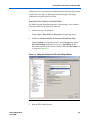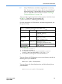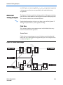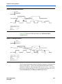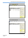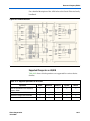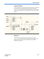
1
Quartus II Handbook, Volume 3
Verification
Preliminary Information
101 Innovation Drive
San Jose, CA 95134
(408) 544-7000
http://www.altera.com
qii5v3_2.1
Copyright © 2004 Altera Corporation. All rights reserved. Altera, The Programmable Solutions Company, the stylized Altera logo, specific device designations, and all other words and logos that are identified as trademarks and/or service marks are, unless noted otherwise, the trademarks and
service marks of Altera Corporation in the U.S. and other countries. All other product or service names are the property of their respective holders. Altera products are protected under numerous U.S. and foreign patents and pending applications, maskwork rights, and copyrights. Altera warrants
performance of its semiconductor products to current specifications in accordance with Altera's standard warranty, but reserves the right to make
changes to any products and services at any time without notice. Altera assumes no responsibility or liability arising out of the application or use of any information, product, or service described herein except as expressly agreed to in writing by Altera
Corporation. Altera customers are advised to obtain the latest version of device specifications before relying on any published information and before placing orders for products or services.
Printed on recycled paper
ii
Preliminary
Altera Corporation
Contents
Chapter Revision Dates ........................................................................... xi
About this Handbook ............................................................................. xiii
How to Contact Altera .......................................................................................................................... xiii
Typographic Conventions .................................................................................................................... xiii
Section I. Simulation
Revision History ....................................................................................................................... Section I–1
Chapter 1. Mentor Graphics
ModelSim Support
Introduction ............................................................................................................................................ 1–1
Background ............................................................................................................................................. 1–1
Software Compatibility ......................................................................................................................... 1–2
Altera Design Flow with ModelSim-Altera Software ...................................................................... 1–3
Functional RTL Simulation ............................................................................................................. 1–3
Gate-Level Timing Simulation ....................................................................................................... 1–4
Functional RTL Simulation .................................................................................................................. 1–4
Functional RTL Simulation Libraries ............................................................................................ 1–4
Simulating VHDL Designs .............................................................................................................. 1–5
Simulating Verilog Designs ............................................................................................................ 1–7
Gate-Level Timing Simulation ........................................................................................................... 1–11
Quartus II Software Output Files for use in the ModelSim-Altera Software ........................ 1–11
Gate Level Simulation Libraries ................................................................................................... 1–12
Simulating VHDL Designs ............................................................................................................ 1–15
Simulation Verilog Designs .......................................................................................................... 1–17
Using the NativeLink Feature with ModelSim ............................................................................... 1–19
Software Licensing & Licensing Set-Up ........................................................................................... 1–20
LM_LICENSE_FILE Variable ....................................................................................................... 1–20
Conclusion ............................................................................................................................................ 1–20
Chapter 2. Synopsys VCS Support
Introduction ............................................................................................................................................
Software Requirements .........................................................................................................................
Using VCS in the Quartus II Design Flow .........................................................................................
Functional RTL Simulations ...........................................................................................................
Post-Synthesis Simulation ...............................................................................................................
Gate-Level Timing Simulation .......................................................................................................
Altera Corporation
2–1
2–1
2–1
2–2
2–4
2–6
iii
Preliminary
Quartus II Handbook, Volume 3
Common VCS Compile Switches ........................................................................................................ 2–8
Using VirSim: The VCS Graphical Interface ...................................................................................... 2–9
VCS Debugging SupportæVCS Command-Line Interface .............................................................. 2–9
Using PLI Routines with the VCS Software .................................................................................... 2–10
Preparing & Linking C Programs to Verilog Code ................................................................... 2–10
Scripting Support ................................................................................................................................. 2–10
Generating a Post-Synthesis Simulation Netlist for VCS ......................................................... 2–11
Generating a Gate-Level Timing Simulation Netlist for VCS .................................................. 2–11
Conclusion ............................................................................................................................................ 2–12
Chapter 3. Cadence NC-Sim Support
Introduction ............................................................................................................................................ 3–1
Software Requirements ......................................................................................................................... 3–1
Simulation Flow Overview .................................................................................................................. 3–1
Functional/RTL Simulation ............................................................................................................ 3–2
Gate-Level Timing Simulation ....................................................................................................... 3–3
Operation Modes .............................................................................................................................. 3–3
Quartus II/NC Simulation Flow Overview ................................................................................. 3–4
Functional/RTL Simulation ................................................................................................................. 3–5
Set Up Your Environment ............................................................................................................... 3–5
Create Libraries ................................................................................................................................ 3–6
Simulating a Design with Memory .............................................................................................. 3–10
Compile Source Code & Testbenches .......................................................................................... 3–11
Elaborate Your Design ................................................................................................................... 3–13
Add Signals to View ...................................................................................................................... 3–15
Simulate Your Design .................................................................................................................... 3–17
Gate-Level Timing Simulation ........................................................................................................... 3–18
Quartus II Simulation Output Files ............................................................................................. 3–18
Quartus II Timing Simulation Libraries ...................................................................................... 3–20
Set Up Your Environment ............................................................................................................. 3–20
Create Libraries .............................................................................................................................. 3–20
Compile the Project Files & Libraries .......................................................................................... 3–21
Elaborate the Design ...................................................................................................................... 3–21
Add Signals to View ...................................................................................................................... 3–23
Simulate Your Design .................................................................................................................... 3–23
Incorporating PLI Routines ................................................................................................................ 3–23
Dynamically Link ........................................................................................................................... 3–24
Dynamically Load .......................................................................................................................... 3–25
Statically Link ................................................................................................................................. 3–28
Scripting Support ................................................................................................................................. 3–29
Generate NC-Sim Simulation Output Files ................................................................................ 3–29
Conclusion ............................................................................................................................................ 3–30
References ............................................................................................................................................. 3–30
iv
Preliminary
Altera Corporation
Contents
Section II. Timing Analysis
Revision History ..................................................................................................................... Section II–1
Chapter 4. Quartus II Timing Analysis
Introduction ............................................................................................................................................ 4–1
Timing Analysis Basics ......................................................................................................................... 4–1
Clock Setup Time (tSU) ................................................................................................................... 4–1
Clock Hold Time (tH) ...................................................................................................................... 4–2
Clock-to-Output Delay (tCO) ......................................................................................................... 4–3
Pin-to-Pin Delay (tPD) ..................................................................................................................... 4–3
Maximum Clock Frequency (fMAX) ............................................................................................. 4–3
Slack .................................................................................................................................................... 4–4
Hold Time Slack ............................................................................................................................... 4–4
Clock Skew ........................................................................................................................................ 4–5
Executing Tcl Script-Based Timing Commands ................................................................................ 4–6
Setting up the Timing Analyzer .......................................................................................................... 4–6
Setting Global Timing Assignments .............................................................................................. 4–7
Specifying Individual Clock Requirements .................................................................................. 4–7
Setting Other Individual Timing Assignments ............................................................................ 4–8
Timing Wizard ................................................................................................................................ 4–12
Timing Analysis Reporting in the Quartus II Software ................................................................. 4–12
Advanced Timing Analysis ................................................................................................................ 4–13
Clock Skew ...................................................................................................................................... 4–13
Multiple Clock Domains ............................................................................................................... 4–15
Multicycle Assignments ................................................................................................................ 4–16
Typical Applications of Multicycle Assignments ...................................................................... 4–19
False Paths ....................................................................................................................................... 4–28
Fixing Hold Time Violations ........................................................................................................ 4–31
Timing Analysis Across Asynchronous Domains ..................................................................... 4–32
Minimum Timing Analysis ................................................................................................................ 4–33
Minimum Timing Analysis Settings ............................................................................................ 4–33
Performing Minimum Timing Analysis ..................................................................................... 4–33
Minimum Timing Analysis Reporting ........................................................................................ 4–34
Third-Party Timing Analysis Software ............................................................................................ 4–34
Advanced Timing Analysis & Reports Using Tcl Scripts .............................................................. 4–34
Conclusion ............................................................................................................................................ 4–37
Chapter 5. Synopsys PrimeTime Support
Introduction ............................................................................................................................................ 5–1
Quartus II Settings to Generate PrimeTime Files .............................................................................. 5–1
Files Generated for the
PrimeTime Environment ...................................................................................................................... 5–2
Sample of Constraints Specified in PrimeTime Format ................................................................... 5–4
PrimeTime Timing Reports .................................................................................................................. 5–4
Sample PrimeTime Timing Report ................................................................................................ 5–5
Running
PrimeTime .............................................................................................................................................. 5–6
Altera Corporation
v
Preliminary
Quartus II Handbook, Volume 3
Conclusion .............................................................................................................................................. 5–6
Section III. Power Estimation & Analysis
Revision History .................................................................................................................... Section III–1
Chapter 6. Early Power Estimation
Introduction ............................................................................................................................................
Excel-Based Power Calculator .............................................................................................................
Estimating Power in the Design Cycle ...............................................................................................
Quartus II Power Report File ...............................................................................................................
Conclusion ..............................................................................................................................................
References ...............................................................................................................................................
6–1
6–1
6–3
6–6
6–8
6–8
Chapter 7. Simulation-Based Power Estimation
Introduction ............................................................................................................................................ 7–1
Power Estimation in the Quartus II Software .................................................................................... 7–2
Estimating Power with EDA Simulation Tools ................................................................................. 7–4
Scripting Support ................................................................................................................................... 7–7
Simulation-Based Power Estimation Settings .............................................................................. 7–7
Generate a Power Input File ........................................................................................................... 7–8
Conclusion .............................................................................................................................................. 7–8
References ............................................................................................................................................... 7–8
Section IV. On-Chip Debugging
Revision History .................................................................................................................... Section IV–2
Chapter 8. Quick Design Debugging Using SignalProbe
Introduction ............................................................................................................................................ 8–1
Using SignalProbe ................................................................................................................................. 8–1
Reserving SignalProbe pins ............................................................................................................ 8–2
Adding SignalProbe Sources .......................................................................................................... 8–3
Assigning I/O Standards ..................................................................................................................... 8–4
Adding Registers for Pipelining .......................................................................................................... 8–4
Performing a SignalProbe Compilation ............................................................................................. 8–5
Running SignalProbe with Smart Compilation ................................................................................ 8–7
Understanding SignalProbe Routing Failures ................................................................................... 8–7
Understanding the Results of a SignalProbe Compilation .............................................................. 8–8
Scripting Support ................................................................................................................................... 8–9
Reserving SignalProbe Pins .......................................................................................................... 8–10
Adding SignalProbe Sources ........................................................................................................ 8–10
Assigning I/O Standards .............................................................................................................. 8–10
Adding Registers for Pipelining ................................................................................................... 8–11
Run SignalProbe Automatically ................................................................................................... 8–11
Run SignalProbe Manually ........................................................................................................... 8–11
vi
Preliminary
Altera Corporation
Contents
Enable or Disable All SignalProbe Routing ................................................................................
Running SignalProbe with Smart Compilation .........................................................................
Allow SignalProbe to Modify Fitting Results ............................................................................
Conclusion ............................................................................................................................................
8–11
8–12
8–12
8–12
Chapter 9. Design Debugging Using the SignalTap II Embedded Logic Analyzer
Introduction ............................................................................................................................................ 9–1
Including the SignalTap II Logic Analyzer in Your Design ............................................................ 9–2
Using the STP File to Create an Embedded Logic Analyzer ..................................................... 9–3
Using the MegaWizard Plug-In Manager to Create your Embedded Logic Analyzer .......... 9–8
Programming the Device for SignalTap II Analysis ....................................................................... 9–12
View Data Samples .............................................................................................................................. 9–12
Advanced Features .............................................................................................................................. 9–12
Preserving FPGA Memory ............................................................................................................ 9–13
Creating Complex Triggers .......................................................................................................... 9–14
Using External Triggers ................................................................................................................. 9–17
Embedding Multiple Analyzers in One FPGA .......................................................................... 9–20
Faster Compilations ....................................................................................................................... 9–20
Time Bars and Next Transition .................................................................................................... 9–22
Saving Captured Data ................................................................................................................... 9–22
Converting Captured Data to Other File Formats ..................................................................... 9–22
Creating Mnemonics for Bit Patterns .......................................................................................... 9–23
Buffer Acquisition .......................................................................................................................... 9–23
Capturing Data to a Specific RAM Type .................................................................................... 9–24
FPGA Resources Used by SignalTap II ....................................................................................... 9–24
Using SignalTap II in a Lab Environment .................................................................................. 9–25
Remote Debugging Using SignalTap II ...................................................................................... 9–25
Signal Preservation ........................................................................................................................ 9–28
Tappable Signals ............................................................................................................................. 9–29
Timing Preservation with SignalTap II Logic Analyzer ........................................................... 9–29
Using SignalTap Il Logic Analyzer to Simultaneously Debug Multiple Designs ................ 9–29
Locating a Node in the Chip Editor ............................................................................................. 9–31
Design Example: Preserving Timing ................................................................................................ 9–32
Design Example: Using SignalTap II Logic Analyzers in SOPC Builder Systems ..................... 9–35
Conclusion ............................................................................................................................................ 9–35
Chapter 10. Design Analysis and Engineering Change Management with Chip Editor
Introduction ..........................................................................................................................................
Background ...........................................................................................................................................
Using the Chip Editor in Your Design Flow ....................................................................................
Chip Editor Overview .........................................................................................................................
Chip Editor Floorplan ....................................................................................................................
Bird’s Eye View ..............................................................................................................................
First (Highest) Level View ............................................................................................................
Second Level View .........................................................................................................................
Third Level View ............................................................................................................................
Resource Property Editor ...................................................................................................................
Altera Corporation
10–1
10–1
10–2
10–3
10–4
10–5
10–6
10–7
10–8
10–9
vii
Preliminary
Quartus II Handbook, Volume 3
The Logic Element (LE) ................................................................................................................. 10–9
The Adaptive Logic Module (ALM) .......................................................................................... 10–10
Supported Changes for an LE/ALM ......................................................................................... 10–11
Properties of the Logic Element ....................................................................................................... 10–12
Mode of Operation ....................................................................................................................... 10–12
LUT Equation ................................................................................................................................ 10–12
LUT Mask ...................................................................................................................................... 10–13
Synchronous Mode ...................................................................................................................... 10–14
Register Cascade Mode ............................................................................................................... 10–14
Properties of an ALM ........................................................................................................................ 10–14
LUT Mask ...................................................................................................................................... 10–14
Extended LUT Mode .................................................................................................................... 10–15
Shared Arithmetic Mode ............................................................................................................. 10–15
FPGA I/O Elements .......................................................................................................................... 10–15
Stratix, Stratix GX, and Stratix II I/O Elements ....................................................................... 10–15
Cyclone I/O Elements ................................................................................................................. 10–17
MAX II I/Os .................................................................................................................................. 10–17
Supported Changes for an I/O Element ................................................................................... 10–18
Editable Properties of I/O Elements ......................................................................................... 10–19
Modifying the PLL Using the Chip Editor ..................................................................................... 10–21
Properties of the PLL ................................................................................................................... 10–21
Adjusting the Duty Cycle ............................................................................................................ 10–22
Adjusting the Phase Shift ............................................................................................................ 10–22
Adjusting the Output Clock Frequency .................................................................................... 10–22
Adjusting the Spread Spectrum ................................................................................................. 10–23
Change Manager ................................................................................................................................ 10–23
Common Applications ...................................................................................................................... 10–24
Gate-Level Register Retiming ..................................................................................................... 10–24
Routing an Internal Signal to an Output Pin ............................................................................ 10–26
Adjust the Phase Shift of a PLL to Meet I/O Timing .............................................................. 10–27
Correcting a Design Flaw ............................................................................................................ 10–27
Example Design: Meeting I/O Timing ........................................................................................... 10–27
Running the Quartus II Timing Analyzer ................................................................................ 10–33
Generating a Netlist for Other EDA Tools ............................................................................... 10–33
Generating a Programming File ................................................................................................. 10–33
Conclusion .......................................................................................................................................... 10–34
Chapter 11. In-System Updating of Memory & Constants
Overview ...............................................................................................................................................
Device & Megafunction Support .......................................................................................................
Creating In-System Configurable Memory and Constants ...........................................................
Running the In-System Memory Content Editor ............................................................................
Instance Manager ...........................................................................................................................
Making Changes .............................................................................................................................
viii
Preliminary
11–1
11–2
11–3
11–4
11–5
11–6
Altera Corporation
Contents
Viewing Memory & Constants in the Hex Editor ..................................................................... 11–7
Programming the Device Using the In-System Memory Content Editor .............................. 11–8
Conclusion ............................................................................................................................................ 11–9
Section V. Formal Verification
Revision History ..................................................................................................................... Section V–1
Chapter 12. Cadence Incisive Conformal Support
Introduction .......................................................................................................................................... 12–1
Formal Verification .............................................................................................................................. 12–1
Equivalence Checking ................................................................................................................... 12–1
Generating the VO File & Incisive Conformal Script ..................................................................... 12–2
Comparing Designs Using Incisive Conformal Software .............................................................. 12–8
Black Boxes in the Incisive Conformal Flow .............................................................................. 12–8
Running the Incisive Conformal Software ................................................................................. 12–9
Known Issues & Limitations ............................................................................................................ 12–11
Conclusion .......................................................................................................................................... 12–11
Index
Altera Corporation
ix
Preliminary
Quartus II Handbook, Volume 3
x
Preliminary
Altera Corporation
Chapter Revision Dates
The chapters in this book, the Quartus II Handbook, Volume 3, were revised on the following dates.
Where chapters or groups of chapters are available separately, part numbers are listed.
Chapter 1. Mentor Graphics
ModelSim Support
Revised:
June 2004
Part number: qii53001-2.0
Chapter 2. Synopsys VCS Support
Revised:
June 2004
Part number: qii53002-2.0
Chapter 3. Cadence NC-Sim Support
Revised:
August 2004
Part number: qii53003-2.0
Chapter 4. Quartus II Timing Analysis
Revised:
June 2004
Part number: qii53004-2.0
Chapter 5. Synopsys PrimeTime Support
Revised:
June 2004
Part number: qii53005-2.0
Chapter 6. Early Power Estimation
Revised:
June 2004
Part number: qii53006-2.0
Chapter 7. Simulation-Based Power Estimation
Revised:
June 2004
Part number: qii53007-2.0
Chapter 8. Quick Design Debugging Using SignalProbe
Revised:
June 2004
Part number: qii53008-2.0
Chapter 9. Design Debugging Using the SignalTap II Embedded Logic Analyzer
Revised:
June 2004
Part number: qii53009-2.0
Altera Corporation
xi
Chapter Revision Dates
Quartus II Handbook, Volume 3
Chapter 10. Design Analysis and Engineering Change Management with Chip Editor
Revised:
June 2004
Part number: qii53010-2.0
Chapter 11. In-System Updating of Memory & Constants
Revised:
August 2004
Part number: qii53012-1.0
Chapter 12. Cadence Incisive Conformal Support
Revised:
June 2004
Part number: qii53011-2.0
xii
Preliminary
Altera Corporation
About this Handbook
This handbook provides comprehensive information about the Altera®
Quartus® II design software, version 4.0.
How to Contact
Altera
Information Type
Technical support
Product literature
For the most up-to-date information about Altera products, go to the
Altera world-wide web site at www.altera.com. For technical support on
this product, go to www.altera.com/mysupport. For additional
information about Altera products, consult the sources shown below.
USA & Canada
All Other Locations
www.altera.com/mysupport/
altera.com/mysupport/
(800) 800-EPLD (3753)
(7:00 a.m. to 5:00 p.m. Pacific Time)
(408) 544-7000 (1)
(7:00 a.m. to 5:00 p.m. Pacific Time)
www.altera.com
www.altera.com
Altera literature services
[email protected] (1)
[email protected] (1)
Non-technical customer
service
(800) 767-3753
(408) 544-7000
(7:30 a.m. to 5:30 p.m. Pacific Time)
FTP site
ftp.altera.com
ftp.altera.com
Note to table:
(1)
You can also contact your local Altera sales office or sales representative.
Typographic
Conventions
Visual Cue
This document uses the typographic conventions shown below.
Meaning
(Part 1 of 2)
Bold Type with Initial
Capital Letters
Command names, dialog box titles, checkbox options, and dialog box options are
shown in bold, initial capital letters. Example: Save As dialog box.
bold type
External timing parameters, directory names, project names, disk drive names,
filenames, filename extensions, and software utility names are shown in bold
type. Examples: fMAX, \qdesigns directory, d: drive, chiptrip.gdf file.
Italic Type with Initial Capital
Letters
Document titles are shown in italic type with initial capital letters. Example: AN
75: High-Speed Board Design.
Altera Corporation
xiii
Preliminary
Typographic Conventions
Visual Cue
Italic type
Quartus II Handbook, Volume 3
Meaning
(Part 2 of 2)
Internal timing parameters and variables are shown in italic type.
Examples: tPIA, n + 1.
Variable names are enclosed in angle brackets (< >) and shown in italic type.
Example: <file name>, <project name>.pof file.
Initial Capital Letters
Keyboard keys and menu names are shown with initial capital letters. Examples:
Delete key, the Options menu.
“Subheading Title”
References to sections within a document and titles of on-line help topics are
shown in quotation marks. Example: “Typographic Conventions.”
Courier type
Signal and port names are shown in lowercase Courier type. Examples: data1,
tdi, input. Active-low signals are denoted by suffix n, e.g., resetn.
Anything that must be typed exactly as it appears is shown in Courier type. For
example: c:\qdesigns\tutorial\chiptrip.gdf. Also, sections of an
actual file, such as a Report File, references to parts of files (e.g., the AHDL
keyword SUBDESIGN), as well as logic function names (e.g., TRI) are shown in
Courier.
1., 2., 3., and
a., b., c., etc.
Numbered steps are used in a list of items when the sequence of the items is
important, such as the steps listed in a procedure.
■
Bullets are used in a list of items when the sequence of the items is not important.
●
•
v
The checkmark indicates a procedure that consists of one step only.
1
The hand points to information that requires special attention.
c
The caution indicates required information that needs special consideration and
understanding and should be read prior to starting or continuing with the
procedure or process.
w
The warning indicates information that should be read prior to starting or
continuing the procedure or processes
r
The angled arrow indicates you should press the Enter key.
f
The feet direct you to more information on a particular topic.
xiv
Preliminary
Altera Corporation
Section I. Simulation
As the design complexity of FPGAs continues to rise, verification
engineers are finding it increasingly difficult to simulate their system-ona-programmable-chip (SOPC) designs in a timely manner. The
verification process is now the bottleneck in the FPGA design flow. You
can perform functional and timing simulation of your design by using the
Quartus® II Simulator. The Quartus II software also provides a wide
range of features for performing simulation of designs in EDA simulation
tools.
This section includes the following chapters:
Revision History
■
Chapter 1, Mentor Graphics ModelSim Support
■
Chapter 2, Synopsys VCS Support
■
Chapter 3, Cadence NC-Sim Support
The table below shows the revision history for Chapters 1 to 3.
Chapter(s) Date / Version
1
June 2004 v2.0
Changes Made
●
●
Updates to tables, figures.
New functionality for Quartus 4.1.
Feb. 2004 v1.0 Initial release
2
June 2004 v2.0
●
●
Updates to tables, figures.
New functionality for Quartus 4.1.
Feb. 2004 v1.0 Initial release
3
Aug. 2004 v2.1
●
New functionality for Quartus 4.1 SP1
June 2004 v2.0
●
Updates to tables, figures.
New functionality for Quartus 4.1.
●
Feb. 2004 v1.0 Initial release
Altera Corporation
Section I–1
Preliminary
Simulation
Section I–2
Preliminary
Quartus II Handbook, Volume 3
Altera Corporation
1. Mentor Graphics
ModelSim Support
qii53001-2.0
Introduction
An Altera® software subscription includes a license for the ModelSimAltera software on a PC or UNIX platform. The ModelSim-Altera
software can be used to perform funtional RTL and gate-level timing
simulations for either VHDL or Verilog HDL designs targeting an Altera
FPGA. This chapter provides step-by-step explanations of how to
simulate your design in the ModelSim-Altera version or the ModelSim
full version. This chapter gives you details on the specific libraries that are
needed for a functional simulation or a gate-level timing simulation.
This document describes ModelSim-Altera software version 5.8c and the
ModelSim PE software version.
f
Background
This document contains references to features available in the Altera
Quartus® II software version 4.1. Please visit the Altera web site,
available at www.altera.com/quartus for information on this Quartus II
software version.
The ModelSim-Altera software version 5.8c is included with your Altera
software subscription, and can be licensed for the PC, Solaris, HP-UX, or
Linux platforms to support either VHDL or Verilog hardware description
language (HDL) simulation. The ModelSim-Altera tool supports VHDL
or Verilog functional simulations and gate-level timing simulations for all
Altera devices.
Table 1–1 describes the differences between the ModelSim-Modeltech
and ModelSim-Altera versions.
Table 1–1. Comparison of ModelSim Versions (Part 1 of 2)
Product Feature
ModelSim SE
ModelSim PE
ModelSim-Altera
ooptionionion
option
Supports only
single-HDL
simulation
Complete HDL debugging environment
v
v
v
Optimized direct compile architecture
v
v
v
Industry-standard scripting
v
v
v
Flexible licensing
v
option
v
100% VHDL, Verilog, mixed-HDL support
Altera Corporation
June 2004
1–1
Preliminary
Quartus II Handbook, Volume 3
Table 1–1. Comparison of ModelSim Versions (Part 2 of 2)
Verilog PLI (1) support. Interfaces Verilog
designs to customer C code and third-party
software
v
VHDL FLI (2) support. Interfaces VHDL
designs to customer C code and third-party
software
v
Advanced debugging features and languageneutral licensing
v
Customizable, user-expandable graphical user
interface (GUI) and integrated simulation
performance analyzer
v
Integrated code coverage analysis and SWIFT
support
v
Accelerated VITAL (3) and Verilog primitives (3
times faster), and register transfer level (RTL)
acceleration (5 times faster)
v
Platform support
PC, UNIX, Linux
v
PC only
v
PC, UNIX, Linux
Note to Table 1–1:
(1)
See www.altera.com/products/software/pld/products/partners/eda-ms.html
Software
Compatibility
f
Table 1–2 shows which specific ModelSim-Altera software version is
compatible with the specific Quartus II software version. ModelSim
versions provided directly from Model Technology do not correspond to
specific Quartus II software versions.
For help on ModelSim-Altera licensing set-up, see “Software Licensing
& Licensing Set-Up” on page 1–20.
Table 1–2. Compatibility Between Software Versions
ModelSim-Altera Software
Quartus II Software (1)
ModelSim-Altera software version 5.7c
Quartus II software version 3.0
ModelSim-Altera software version 5.7e
Quartus II software version 4.0
ModelSim-Altera software version 5.8c
Quartus II software version 4.1
Note to Table 1–2:
(1)
ModelSim-Altera precompiled libraries are updated with Quartus II release and service packs and are generally
available for download on Altera’s web site.
1–2
Preliminary
Altera Corporation
June 2004
Altera Design Flow with ModelSim-Altera Software
Altera Design
Flow with
ModelSimAltera Software
Figure 1–1 illustrates an Altera design flow using the ModelSim-Altera
software or ModelSim Full Version:
■
■
Functional RTL simulations
Gate-level timing simulations
Figure 1–1. Altera Design Flow with ModelSim-Altera and Quartus II Software
Altera IP
Design Entry
Testbench
Functional Simulation
Functional
Models
Synthesis
Place-and-Route
Verilog
Output
File (.vo)
Standard Delay
Format Output
File (.sdo)
Gate-Level Simulation
Gate-Level
Models
Functional RTL Simulation
Functional RTL simulations verify the functionality of the design before
synthesis and place-and route. These simulations are independent of any
Altera FPGA architecture implementation. Once the HDL designs are
verified to be functionally correct, the next step is to synthesize the design
and use the Quartus II software for place-and-route.
Altera Corporation
June 2004
1–3
Preliminary
Quartus II Handbook, Volume 3
Gate-Level Timing Simulation
Place-and-route in the Quartus II software produces a design netlist (.vo
or .vho file) and a Standard Delay Format (SDF) output (.sdo) file used for
a gate-level timing simulation in the ModelSim-Altera software. The
design netlist output file is a netlist of the design mapped to
architecture-specific primitives such as logic elements and I/O elements.
The SDF file contains delay information for each architecture primitive
and routing element specific to the design. Together, these files provide an
accurate simulation of the design for the selected Altera FPGA
architecture.
Functional RTL
Simulation
A functional RTL simulation is performed before a gate-level simulation
and verifies the functionality of the design before place-and-route. This
section provides detailed instructions on how to perform a functional
RTL simulation in the ModelSim-Altera software and highlights some of
the differences in performing similar steps in the Model TechnologyTM
ModelSim software versions for VHDL and Verilog HDL designs.
Functional RTL Simulation Libraries
LPM and Altera Megafunction Functional RTL Simulation Models
To simulate designs containing LPM functions or MegaWizard®
Plug-In Manager-generated functions, use the following Altera
functional simulation models:
■
■
1
f
220model.v (for Verilog HDL)
220pack.vhd and 220model.vhd (for VHDL)
When you are simulating a design that uses VHDL-1987, use
220model_87.vhd.
For more information on LPM functions, see the Quartus II Help.
Altera Megafunction Simulation Models
To simulate a design that contains Altera Megafunctions, use the
following simulation models:
■
■
1
1–4
Preliminary
altera_mf.v (for Verilog HDL)
altera_mf.vhd and altera_mf_components.vhd (for VHDL)
When you are simulating a design that uses VHDL-1987, use
altera_mf_87.vhd.
Altera Corporation
June 2004
Functional RTL Simulation
Table 1–3 shows the location of the simulation model files in the
Quartus II software and the ModelSim-Altera software.
Table 1–3. Location of LPM Simulation Models
Software
Location
Quartus II
<Quartus II installation directory>\eda\sim_lib\ (1)
ModelSim-Altera
(PC)
<ModelSim-Altera installation directory>\altera\<HDL>\220model\(2)
ModelSim-Altera
(UNIX)
<ModelSim-Altera installation directory>/modeltech/altera/<HDL>/220model/(1)
Note to Table 1–3:
(1)
(2)
For Model Technology’s ModelSim, use the files provided with the Quartus II software.
Compile 220pack.vhd before 220model.vhd.
Table 1–4 shows the location of these files in the Quartus II software and
the ModelSim-Altera software.
Table 1–4. Location of Altera Megafunction Simulation Models
Software
Location
Quartus II
<Quartus II installation directory>\eda\sim_lib \ (1)
ModelSim-Altera
(PC)
<ModelSim-Altera installation directory>\altera\<HDL>\altera_mf\
ModelSim-Altera
(UNIX)
<ModelSim-Altera installation directory>/modeltech/altera/<HDL>/altera_mf/
Note to Table 1–4:
(1)
For Model Technology’s ModelSim, use the files provided with the Quartus II software.
Simulating VHDL Designs
The following instructions will help you to perform a functional RTL
simulation for VHDL designs in the ModelSim-Altera software.
1
The following steps assume you have already created a
ModelSim project.
Create Simulation Libraries
1
Creating a simulation library is not required if you are using the
ModelSim-Altera software.
Altera Corporation
June 2004
1–5
Preliminary
Quartus II Handbook, Volume 3
Simulation libraries are needed to simulate a design that contains an LPM
function or an Altera megafunction. If you are using the Model
TechnologyTM ModelSim software version, you need to create the
simulation libraries and correctly link them to your design.
1.
Choose New > Library (File menu).
2.
In the Create a New Library dialog box select a new Library and a
logical linking to it.
3.
Enter the name of the newly created library in the Library Name
box.
4.
Click OK.
vlib altera_mfr
vmap altera_mf altera_mfr
vlib lpmr
vmap lpm lpmr
1
The name of the libraries should be altera_mf (for Altera
megafunctions) and lpm (for LPM and Megawizard-generated
entities).
Compile Simulation Models into Simulation Libraries
1
The following steps are not required for the ModelSim-Altera
software.
1.
Choose Add to Project (File menu) and select Existing File.
2.
Browse to the <quartus installation folder>/eda/sim_lib> and add the
necessary simulation model files to your project.
3.
Select the simulation model file and select Properties (View menu).
4.
Set the Compile to Library to the correct library.
1
The altera_mf.vhd should be compiled into the altera_mf
library. The 220model.vhd should be compiled into the lpm
library.
vcom -work altera_mf <quartus installation
directory>/eda/sim_lib/altera_mf_components.vhd> r
vcom -work altera_mf <quartus installation folder/eda/sim_lib
/altera_mf.vhd> r
1–6
Preliminary
Altera Corporation
June 2004
Functional RTL Simulation
vcom -work lpm <quartus installation folder/eda/sim_lib /220pack.vhd> r
vcom -work lpm <quartus installation folder/eda/sim_lib /220model.vhd> r
Compile Testbench and Design Files into Work Library
1. Select Compile All (Compile menu) or click the Compile All
toolbar icon
2.
Resolve compile-time errors before proceeding to “Loading the
Design” below.
vcom -work work <my_testbench.vhd> <my_design_files.vhd>r
Loading the Design
1. Select Simulate (Simulate menu).
2.
Expand the work library in the Simulate dialog box.
3.
Select the top-level design unit (your testbench). Select OK in the
Simulate dialog box.
vsim work.<my_testbench>r
Running the Simulation
1. Choose Signals and Wave (View menu).
view signalsr
view waver
2.
Drag signals to monitor from the Signals window and drop them
into the Wave window.
add wave /<signal name>r
3.
At the prompt type the following:
run <time period>r
Simulating Verilog Designs
The following instructions provide step-by-step instructions on
performing functional RTL simulation for Verilog designs in the
ModelSim-Altera software.
1
Altera Corporation
June 2004
The following steps assume you have already created a
ModelSim project.
1–7
Preliminary
Quartus II Handbook, Volume 3
Create Simulation Libraries
1
Creating a simulation library is not required for the ModelSimAltera software.
Simulation libraries are needed to properly simulate a design that
contains an LPM function or an Altera megafunction. If you are using the
Model Technology ModelSim software version, you need to create the
simulation libraries and correctly link them to your design.
1.
Choose New > Library (File menu).
2.
In the Create a New Library dialog box select a new Library and a
logical linking to it.
3.
Enter the name of the newly created library in the Library Name
box.
4.
Click OK.
vlib altera_mfr
vmap altera_mf altera_mfr
vlib lpmr
vmap lpm lpmr
1
The name of the libraries should be altera_mf (for Altera
megafunctions) and lpm (for LPM and Megawizard-generated
entities).
1
This process is not required for the ModelSim-Altera version
because a set of pre-compiled libraries are created when you
install the ModelSim-Altera software.
Compile Simulation Models into Simulation Libraries
1
The following steps are not required for the ModelSim-Altera
software.
1–8
Preliminary
1.
Choose Add to Project (File menu) and select Existing File.
2.
Browse to the <quartus installation folder>/eda/sim_lib> and add the
necessary simulation model files to your project.
3.
Select the simulation model file and select Properties (View menu).
4.
Set the Compile to Library to the correct library.
Altera Corporation
June 2004
Functional RTL Simulation
1
The altera_mf.v should be compiled into the altera_mf library.
Compile the 220model.v into the lpm library.
vlog -work altera_mf
/altera_mf.v> r
<quartus installation folder/eda/sim_lib
vlog -work lpm <quartus installation folder/eda/sim_lib /220model.v>r
Compile Testbench and Design Files into Work Library
1. Select Compile All (Compile menu) or click the Compile All
toolbar icon
2.
Resolve compile-time errors before proceeding to “Loading the
Design” below.
vlog -work work <my_testbench.v> <my_design_files.v>r
Loading the Design
1. Select Simulate (Simulate menu).
2.
Click the Libraries tab in the Load Design dialog box.
3.
In the Search Libraries box, click Add.
4.
Specify the location to the lpm or altera_mf simulation libraries.
1
If you are using the ModelSim-Altera version see Table 1–3 and
Table 1–5 for the location of the precompiled simulation
libraries.
1
If you are using the ModelSim-Modeltech version, browse to the
library that was created earlier.
5.
In the Load Design dialog box, click the Design tab.
6.
Expand the work library in the Simulate dialog box.
7.
Select the top-level design unit (your testbench). Select OK in the
Simulate dialog box.
vsim -L <location of the altera_mf library> -L <location of the lpm
library> work.<my_testbench>r
Running the Simulation
1. Choose Signals and Wave (View menu).
Altera Corporation
June 2004
1–9
Preliminary
Quartus II Handbook, Volume 3
view signalsr
view waver
2.
Drag signals to monitor from the Signals window and drop them
into the Wave window.
add wave /<signal name>r
3.
At the prompt type the following:
run <time period>r
Verilog Functional RTL Simulation with Altera Memory Blocks
You can simulate your design containing complex memory blocks such as
LPM_RAM_DP and ALTSYNCRAM using either ModelSim software
version.
These memory blocks can be configured with power-up data via a
hexidecimal (.hex) or Memory Initialization File (.mif). The LPM_FILE
parameter included in the MegaWizard-generated file points to the path
of the HEX file or MIF that is used to initialize the memory block. You can
create a HEX file or MIF through the Quartus II software.
Neither ModelSim software version can directly read a HEX file or MIF
format. Therefore, to allow functional simulation of Altera memory
blocks in the ModelSim software, you must perform the following steps:
1.
Convert a HEX file or MIF to a RAM Initialization File (.rif).
2.
Modify of the MegaWizard-generated file.
3.
Compile the nopli.v file.
Converting a HEX File or MIF to a RIF
A RIF is an ASCII text file that you use with tools from electronic design
automation (EDA) vendors. Create a RIF by converting an existing MIF
or HEX file using the Export command in the Quartus II software. This
option is available through the File menu.
Modifying the MegaWizard-Generated File
You must modify the MegaWizard-generated file so that it includes the
path to the newly created RIF. You must modify the LPM_FILE
parameter. The following example shows the entry that you must change:
1–10
Preliminary
Altera Corporation
June 2004
Gate-Level Timing Simulation
lpm_ram_dp_component.lpm_outdata = "UNREGISTERED",
lpm_ram_dp_component.lpm_file = "<path to RIF>"
lpm_ram_dp_component.use_eab = "ON",
Compiling nopli.v
The nopli.v file is included in the s<path to Quartus II
installation>\eda\sim_lib directory. This file contains the following
definition:
`define NO_PLI 1
This basic definition instructs the ModelSim compile to read in the RIF.
Gate-Level
Timing
Simulation
Gate-level timing simulation is a post place-and-route simulation to
verify the operation of the design after the worst-case timing delays have
been calculated. This section provides detailed instructions on how to
perform gate-level timing simulation in the ModelSim-Altera software
and highlights differences in performing similar steps in the
Model Technology ModelSim software versions for VHDL and Verilog
HDL designs.
Quartus II Software Output Files for use in the ModelSim-Altera
Software
To perform gate-level timing simulation, the ModelSim-Altera software
requires information on how the design was placed into device-specific
architectural blocks. The Quartus II software provides this information in
the form of .vo for Verilog HDL and .vho for VHDL output files. The
accompanying timing information is stored in the .sdf file, which
annotates the delay for the elements found in the .vo or .vho output file.
To generate the VO or VHO output files, perform the following steps:
1.
Choose EDA Tool Settings (Assignments menu).
2.
In the Simulation Tool box:
3.
Altera Corporation
June 2004
a.
If you are using ModelSim-Altera, select ModelSim OEM
(VHDL/Verilog HDL output from Quartus II).
b.
If you are using Model Technology's ModelSim, select
ModelSim (VHDL/Verilog HDL output from Quartus II).
Click OK.
1–11
Preliminary
Quartus II Handbook, Volume 3
4.
Compile the project.
5.
The Quartus II output files are located in the <full path to
project>\simulation\ModelSim\ directory.
Gate Level Simulation Libraries
Table 1–5 provides a description of the various ModelSim-Altera
precompiled device libraries.
Table 1–5. Various ModelSim-Altera Precompiled Device Libraries
Library
Description
maxii
Precompiled library for MAX® II devices
stratixii
Precompiled library for Stratix® II devices
stratix
Precompiled library for Stratix device designs
stratixgx
Precompiled library for Stratix GX device designs
stratixgx_gxb Precompiled library for Stratix GX device designs using the Gigabit Transceiver Block (altgxb
Megafunction)
cyclone
Precompiled library for Cyclone™ device designs
apexii
Precompiled library for APEX™ II device designs
apex20k
Precompiled library for APEX™ 20K device designs
apex20ke
Precompiled library for APEX 20KC, APEX 20KE devices and ARM®-based Excalibur™ designs
mercury
Precompiled library for Mercury™ device designs
flex10ke
Precompiled library for FLEX® 10KE and ACEX™ 1K device designs
flex6000
Precompiled library for FLEX 6000 device designs
max
Precompiled library for MAX 7000 and MAX 3000 device designs
Table 1–6 shows the location of the timing simulation libraries in the
ModelSim-Altera software for Verilog HDL for PCs.
Table 1–6. Location of Timing Simulation Libraries for ModelSim-Altera for Verilog HDL on a PC
(Part 1 of 2)
Library
Verilog HDL
maxii
<ModelSim-Altera installation directory>\altera\verilog\maxii\
stratixii
<ModelSim-Altera installation directory>\altera\verilog\stratixii\
stratix
<ModelSim-Altera installation directory>\altera\verilog\stratix\
stratixgx
<ModelSim-Altera installation directory>\altera\verilog\stratixgx\
stratixgx_gxb
<ModelSim-Altera installation directory>\altera\verilog\stratixgx_gxb\
1–12
Preliminary
Altera Corporation
June 2004
Gate-Level Timing Simulation
Table 1–6. Location of Timing Simulation Libraries for ModelSim-Altera for Verilog HDL on a PC
(Part 2 of 2)
Library
Verilog HDL
cyclone
<ModelSim-Altera installation directory>\altera\verilog\cyclone\
apexii
<ModelSim-Altera installation directory>\altera\verilog\apexii\
apex20k
<ModelSim-Altera installation directory>\altera\verilog\apex20k\
apex20ke
<ModelSim-Altera installation directory>\altera\verilog\apex20ke\
mercury
<ModelSim-Altera installation directory>\altera\verilog\mercury\
flex10ke
<ModelSim-Altera installation directory>\altera\verilog\flex10ke\
flex6000
<ModelSim-Altera installation directory>\altera\verilog\flex6000\
max
<ModelSim-Altera installation directory>\altera\verilog\max\
Table 1–7 shows the location of the timing simulation libraries in the
ModelSim-Altera software for VHDL for PCs.
Table 1–7. Location of Timing Simulation Library Files for ModelSim-Altera for VHDL on a PC
Library
VHDL
maxii
<ModelSim-Altera installation directory>\altera\vhdl\maxii\
stratixii
<ModelSim-Altera installation directory>\altera\vhdl\stratixii\
stratix
<ModelSim-Altera installation directory>\altera\vhdl\stratix\
stratixgx
<ModelSim-Altera installation directory>\altera\vhdl\stratixgx\
stratixgx_gxb
<ModelSim-Altera installation directory>\altera\vhdl\stratixgx_gxb\
cyclone
<ModelSim-Altera installation directory>\altera\vhdl\cyclone\
apexii
<ModelSim-Altera installation directory>\altera\vhdl\apexii\
apex20ke
<ModelSim-Altera installation directory>\altera\vhdl\apex20ke\
apex20k
<ModelSim-Altera installation directory>\altera\vhdl\apex20k\
flex10ke
<ModelSim-Altera installation directory>\altera\vhdl\flex10ke\
flex6000
<ModelSim-Altera installation directory>\altera\vhdl\flex6000\
mercury
<ModelSim-Altera installation directory>\altera\vhdl\mercury\
max
<ModelSim-Altera installation directory>\altera\vhdl\max\
Altera Corporation
June 2004
1–13
Preliminary
Quartus II Handbook, Volume 3
Table 1–8 shows the location of the timing simulation libraries in the
ModelSim-Altera software for Verilog HDL for UNIX.
Table 1–8. Location of Timing Simulation Libraries for ModelSim-Altera for Verilog HDL with UNIX
Library
Verilog HDL
maxii
<ModelSim-Altera installation directory>/modeltech/altera/verilog/maxii/
stratixii
<ModelSim-Altera installation directory>/modeltech/altera/verilog/stratixii/
stratix
<ModelSim-Altera installation directory>/modeltech/altera/verilog/stratix/
stratixgx
<ModelSim-Altera installation directory>/modeltech/altera/verilog/stratixgx/
stratixgx_gxb <ModelSim-Altera installation directory>/modeltech/altera/verilog/stratixgx_gxb/
cyclone
<ModelSim-Altera installation directory>/modeltech/altera/verilog/cyclone/
apexii
<ModelSim-Altera installation directory>/modeltech/altera/verilog/apexii/
apex20k
<ModelSim-Altera installation directory>/modeltech/altera/verilog/apex20k/
apex20ke
<ModelSim-Altera installation directory>/modeltech/altera/verilog/apex20ke/
mercury
<ModelSim-Altera installation directory>/modeltech/altera/verilog/mercury/
flex10ke
<ModelSim-Altera installation directory>/modeltech/altera/verilog/flex10ke/
flex6000
<ModelSim-Altera installation directory>/modeltech/altera/verilog/flex6000/
max
<ModelSim-Altera installation directory>/modeltech/altera/verilog/max/
Table 1–9 shows the location of the timing simulation libraries in the
ModelSim-Altera software for VHDL for UNIX.
Table 1–9. Location of Timing Simulation Libraries for ModelSim-Altera for VHDL with UNIX (Part 1 of 2)
Library
maxii
VHDL
<ModelSim-Altera installation directory>/modeltech/altera/vhdl/maxii/
stratixii
<ModelSim-Altera installation directory>/modeltech/altera/vhdl/stratixii/
stratix
<ModelSim-Altera installation directory>/modeltech/altera/vhdl/stratix/
stratixgx
<ModelSim-Altera installation directory>/modeltech/altera/vhdl/stratixgx/
stratixgx_gxb
<ModelSim-Altera installation directory>/modeltech/altera/vhdl/stratixgx_gxb/
cyclone
<ModelSim-Altera installation directory>/modeltech/altera/vhdl/cyclone/
apexii
<ModelSim-Altera installation directory>/modeltech/altera/vhdl/apexii/
apex20k
<ModelSim-Altera installation directory>/modeltech/altera/vhdl/apex20k/
apex20ke
<ModelSim-Altera installation directory>/modeltech/altera/vhdl/apex20ke/
mercury
<ModelSim-Altera installation directory>/modeltech/altera/vhdl/mercury/
flex10ke
<ModelSim-Altera installation directory>/modeltech/altera/vhdl/flex10ke/
1–14
Preliminary
Altera Corporation
June 2004
Gate-Level Timing Simulation
Table 1–9. Location of Timing Simulation Libraries for ModelSim-Altera for VHDL with UNIX (Part 2 of 2)
Library
VHDL
flex6000
<ModelSim-Altera installation directory>/modeltech/altera/vhdl/flex6000/
max
<ModelSim-Altera installation directory>/modeltech/altera/vhdl/max/
If you are using the ModelSim-Modeltech version for your timing
simulation, libraries are available in the Quartus II software at the
following location: <Quartus II installation directory>\eda\sim_lib\.
Model Technology ModelSim software users must use the files provided
with the Quartus II software.
Simulating VHDL Designs
The following provides step-by-step instructions for performing gatelevel timing simulation for VHDL designs.
1
The following steps assume you have already created a
ModelSim project. For additional information see “Altera
Design Flow with ModelSim-Altera Software” on page 1–3.
Create Simulation Libraries
If you are using the Model Technology ModelSim software version, create
the gate-level simulation libraries and correctly link them to your design.
1
This process is not required for the ModelSim-Altera version
because a set of pre-compiled libraries are created when you
install the software.
1.
Select New Library (File menu).
2.
In the Create a New Library dialog box, select a new Library and a
logical linking to it.
3.
Enter in the name of the newly created library in the Library Name
box.
4.
Click OK.
vlib stratixiir
vmap stratixii stratixiir
Altera Corporation
June 2004
1–15
Preliminary
Quartus II Handbook, Volume 3
Compile Simulation Models into Simulation Libraries
1
This process is not required for the ModelSim-Altera version
because a set of pre-compiled libraries are created when you
install the software.
1.
Select Add to Project (File menu), then select Existing File.
2.
Browse to the <quartus installation folder>/eda/sim_lib> and add the
necessary gate level simulation files to your project.
3.
Select the simulation model file and select Properties (View menu).
4.
Set the Compile to Library to the correct library.
vcom -work altera_mf <quartus installation folder/eda/sim_lib
/stratixii_components.vhd> r
vcom -work altera_mf <quartus installation folder/eda/sim_lib
/stratixii.vhd> r
Compile Testbench and VHO into Work Library
1. Choose Compile All (Compile menu) or click the Compile All
toolbar icon.
2.
Resolve any compile time errors before proceeding to Loading the
Design.
vcom -work work <my_testbench.vhd> <my_vhdl_output_file.vho>r
Loading the Design
1. Select Simulate (Simulate menu).
2.
Click the SDF tab and click Add.
3.
Specify the location of the SDF file and click OK.
4.
In the Library list (Design tab), select the work library.
5.
Expand the work library in the Simulate dialog box.
6.
Select the top-level design unit (your testbench) and select OK in the
Simulate dialog box.
vsim -sdftyp work.<my_testbench>r
Running the Simulation
1. Choose Signals and Wave (View menu).
1–16
Preliminary
Altera Corporation
June 2004
Gate-Level Timing Simulation
view signalsr
view waver
2.
Drag signals to monitor from the Signals window and drop them
into the Wave window.
add wave /<signal name>r
3.
At the prompt type the following:
run <time period>r
Simulation Verilog Designs
The following provides step-by-step instructions on performing gatelevel timing simulation for Verilog HDL designs in the ModelSim-Altera
software.
1
The following steps assume you have already created a
ModelSim project. For additional information see “Altera
Design Flow with ModelSim-Altera Software” on page 1–3.
Create Simulation Libraries
1
This process is not required for the ModelSim-Altera version
because a set of pre-compiled libraries are created when you
install the software.
If you are using the Model Technology ModelSim software version, you
need to create the simulation libraries and correctly link them to your
design.
1.
Choose New Library (File menu).
2.
In the Create a New Library dialog box, select a new library and a
logical linking to it.
3.
Enter the name of the newly created library in the Library Name.
4.
Click OK.
vlib stratixiir
vmap stratixii stratixiir
Compile Simulation Models into Simulation Libraries
1
This process is not required for the ModelSim-Altera version
because a set of pre-compiled libraries are created when you
install the software.
Altera Corporation
June 2004
1–17
Preliminary
Quartus II Handbook, Volume 3
1.
Select Add to Project (File menu) and select Existing File.
2.
Browse to the <quartus installation folder>/eda/sim_lib> and add the
necessary simulation model files to your project.
3.
Select the simulation model file and select Properties (View menu).
4.
Set the Compile to Library to the correct library.
vlog -work stratixii <quartus installation folder/eda/sim_lib
/startixii_atoms.v> r
Compile Testbench and VO into Work Library
1. Select Compile All (Compile menu) or click the Compile All
toolbar icon.
2.
Resolve any compile time errors before proceeding to Loading the
Design.
vlog -work work <my_testbench.v> <my_verilog_output_file.vo>r
Loading the Design
1. Select Simulate (Simulate menu).
2.
In the Load Design dialog box, click the Libraries tab.
3.
In the Search Libraries box, click Add.
4.
Specify the location to the gate level simulation library.
1
If you are using the ModelSim-Altera version, refer to Tables 1–5
and 1–6 for the location of the precompiled simulation libraries.
1
If you are using the ModelSim-Modeltech version, browse to the
library that was created earlier.
5.
In the Load Design dialog box, click the Design tab.
6.
Expand the work library in the Simulate dialog box.
7.
Select the top-level design unit (your testbench) and select OK in the
Simulate dialog box.
vsim -L <location of the gate level simulation library> work.<my_testbench>r
Running the Simulation
1. Choose Signals and Wave (View menu).
1–18
Preliminary
Altera Corporation
June 2004
Using the NativeLink Feature with ModelSim
view signalsr
view waver
2.
Drag signals to monitor from the Signals window and drop them
into the Wave window.
add wave /<signal name>r
3.
At the prompt type the following:
run <time period>r
Using the
NativeLink
Feature with
ModelSim
The NativeLink feature in the Quartus II software facilitates the seamless
transfer of information between the Quartus II software and EDA tools
and allows you to run ModelSim within the Quartus II software.
To run an EDA simulation or timing analysis tool automatically after a
compilation in the Quartus II software:
1.
Select EDA Tool Settings (Assignments menu) and set the
Simulation Tool Name to one of the following:
ModelSim (Verilog Output from Quartus II)
ModelSim (VHDL Output from Quartus II)
ModelSim-Altera (Verilog Output from Quartus II)
ModelSim-Altera (VHDL Output from Quartus II)
1
2.
Make sure you turn on Run this tool automatically after
compilation in the Simulation page under EDA Tool Settings
in the Settings dialog box (Assignments menu).
Compile the design.
The Quartus II software creates a simulation work directory, compiles the
appropriate design files and simulation libraries, and launches the EDA
simulation tool.
UNIX workstations only: to run ModelSim automatically from the
Quartus II software using the NativeLink feature, you must add the
following environment variables to your .cshrc:
QUARTUS_INI_PATH <ModelSim installation directory> r
Altera Corporation
June 2004
1–19
Preliminary
Quartus II Handbook, Volume 3
Software
Licensing &
Licensing SetUp
License the ModelSim-Altera software through a parallel port software
guard (T-guard), FIXEDPC license, or a network FLOATNET or
FLOATPC license. Each Altera software subscription includes a license to
either VHDL or Verilog HDL. Network licenses with multiple users may
have their licenses split between VHDL and Verilog HDL in any ratio.
1
USB is not supported.
Obtain licenses for ModelSim-Altera software from the Altera web site at
www.altera.com. Get licensing information for Model Technology’s
ModelSim directly from Model Technology. See Figure 1–2 for the set-up
process.
1
For ModelSim-Altera versions prior to 5.5b, use the PCLS utility,
included with the software, to set up the license.
Figure 1–2. ModelSim-Altera Licensing Set-up Process
Initial installation
Yes
Is
ModelSim-Altera
properly licensed?
No
Set the
LM_LICENSE_FILE
variable
Finish
LM_LICENSE_FILE Variable
Altera recommends setting the LM_LICENSE_FILE environment
variable to the location of the license file.
Conclusion
1–20
Preliminary
Using the ModelSim-Altera simulation software within the Altera FPGA
design flow enables Altera software users to easily and accurately
perform functional and timing simulation on their designs. Proper
verification of designs at the functional and post place-and-route stages
using the ModelSim-Altera software helps ensure design functionality
and success and, ultimately, a quick time-to-market.
Altera Corporation
June 2004
Conclusion
Altera Corporation
June 2004
1–21
Preliminary
Quartus II Handbook, Volume 3
1–22
Preliminary
Altera Corporation
June 2004
2. Synopsys VCS Support
qii53002-2.0
Introduction
f
Software
Requirements
This chapter is a getting-started guide to using the Synopsys VCS
software to simulate designs targeting Altera® FPGAs. It provides a stepby-step explanation of how to perform functional simulations, postsynthesis simulations, and gate-level timing simulations using the VCS
software.
This document contains references to features available in the Altera
Quartus® II software version 4.1. For more information on the Quartus II
software version 4.1, go to the Altera web site at www.altera.com.
In order to properly simulate your design using VCS, you must first
install the Quartus II software.
Table 2–1 shows the supported Quartus II-VCS version compatibility.
Table 2–1. Supported Quartus II & VCS Software Version Compatibility
Synopsys
f
Using VCS in the
Quartus II
Design Flow
Altera Corporation
June 2004
Altera
VCS software version 7.0
Quartus II software version 3.0
VCS software version 7.0.1
Quartus II software version 4.0
VCS software version 7.1.1
Quartus II software version 4.1
See the Quartus II Installation & Licensing for PCs or the Quartus II
Installation & Licensing for UNIX and Linux Workstation manuals for more
information on installing the software and the directories created during
the Quartus II software installation.
The VCS software supports the following types of simulation:
■
■
■
Functional RTL simulations
Post-synthesis simulations
Gate-level timing simulations
2–1
Preliminary
Quartus II Handbook, Volume 3
Figure 2–1 shows the VCS and Quartus II software design flow.
Figure 2–1. Altera Design Flow with the VCS & Quartus II Software
Altera IP
Design Entry
Testbench
Functional RTL Simulation
Functional
Models
Synthesis
Post-Synthesis
Simulation
PostSynthesis
Models
Place-and-Route
Verilog Output
File (.vo)
Standard Delay
Format Output
File (.sdo)
Gate-Level Timing
Simulation
Gate-Level
Models
Functional RTL Simulations
Functional RTL simulations verify the functionality of the design before
synthesis and place-and-route. These simulations are independent of any
Altera FPGA architecture implementation. Once the HDL designs are
verified to be functionally correct, the next step is to synthesize the design
and use the Quartus II software for place-and-route.
To functionally simulate an Altera FPGA design in the VCS software that
uses Altera IP megafunctions, or library of parameterized modules (LPM)
functions, you must include certain libraries during the compilation.
2–2
Preliminary
Altera Corporation
June 2004
Using VCS in the Quartus II Design Flow
Table 2–2 summarizes the Verilog library files that are required to compile
library of parameterized modules (LPM) functions and Altera
megafunctions.
Table 2–2. Altera Verilog Functional/Behavioral Simulation Library Files
Library File
Description
altera_mf.v
Libraries that contain simulation models for Altera
megafunctions.
stratixgx_mf.v (1)
Libraries that contain simulation models for Stratix™ GX
devices.
220model.v
Libraries that contain simulation models for Altera LPM
functions version 2.2.0.
sgate.v
Libraries that contain simulation models for Altera IP
Note to Table 2–2:
(1)
When performing a functional RTL simulation of StratixGX design you will need
to compile the stratixgx_mf.v, sgate.v, & 220model.v
The files in Table 2–2 are installed with a Quartus II installation. You can
find these files in the <path to Quartus II installation>\eda\sim_lib
directory.
The following VCS command describes the command-line syntax to
perform a functional simulation with a pre-existing library:
vcs -R <test bench>.v <design name>.v
–v <Altera library file>.v
Functional RTL Simulation with Altera Memory Blocks
The VCS software supports functional simulation of complex Altera
memory blocks such as lpm_ram_dp and altsyncram. You can create
these memory blocks with the Quartus II MegaWizard® Plug-In Manager,
which can be initialized with power-up data via a hexidecimal (.hex) or
Memory Initialization File (.mif). The lpm_file parameter included in
the MegaWizard-generated file points to the path of the HEX file or MIF
that is used to initialize the memory block. You can create a HEX file or
MIF through the Quartus II software.
However, the VCS software cannot read a HEX file or MIF format.
Therefore, in order to perform functional simulation of Altera memory
blocks in the VCS software, you must perform the following steps:
1.
Altera Corporation
June 2004
Convert a HEX file or MIF to a RAM Initialization File (.rif)
2–3
Preliminary
Quartus II Handbook, Volume 3
f
2.
Modify the MegaWizard-generated file
3.
Compile the nopli.v file
For more information on creating a MIF, see Quartus II Help.
Converting a HEX File or MIF to a RIF
A RIF is an ASCII text file that you can use with tools from electronic
design automation (EDA) vendors. You can create a RIF by converting an
existing MIF or HEX file using the Export Current File As command in
the Quartus II software. This option is available through the File menu
while the Quartus II memory editor is open.
Modifying the MegaWizard-Generated File
You must modify the MegaWizard-generated file so that it includes the
path to the newly created RIF. You must modify the lpm_file
parameter. The following example shows the entry that you must change:
lpm_ram_dp_component.lpm_outdata = "UNREGISTERED",
lpm_ram_dp_component.lpm_file = "<path to RIF>"
lpm_ram_dp_component.use_eab = "ON",
Compiling nopli.v
The nopli.v file is included in the
<path to Quartus II installation>\eda\sim_lib directory. This file
contains the following definition:
`define NO_PLI 1
This basic definition instructs the VCS compile to read in the RIF.
The following VCS command simulates a design that includes Altera
RAM blocks that require memory initialization:
vcs -R <path to Quartus installation>\eda
\sim_lib\nopli.v <test bench>.v
<design name>.v –v <Altera library file>.v
Post-Synthesis Simulation
A post-synthesis simulation verifies the functionality of a design after
synthesis has been performed. You can create a post-synthesis netlist in
the Quartus II software and use this netlist to perform a post-synthesis
2–4
Preliminary
Altera Corporation
June 2004
Using VCS in the Quartus II Design Flow
simulation in VCS. Once the post-synthesis version of the design has been
verified, the next step is to place-and-route the design in the target
architecture using the Quartus II Fitter.
Generating a Post-Synthesis Simulation Netlist
The following steps describe the process of generating a post-synthesis
simulation netlist in the Quartus II software:
1.
Perform Analysis & Synthesis:
Choose Start > Start Analysis & Synthesis (Processing menu).
2.
Enable the Generate Netlist for Functional Simulation Only:
Choose Settings (Assignments menu). In the Category list, select
EDA Tool Settings (expand if necessary) > Simulation. In the
Simulation section of the window, choose VCS in the Tool name list,
as shown in Figure 2–2.
Figure 2–2. Setting the Tool Name to VCS in the Settings Window
3.
Altera Corporation
June 2004
Run the EDA Netlist Writer:
2–5
Preliminary
Quartus II Handbook, Volume 3
Choose Start > Start EDA Netlist Writer (Processing menu).
During the EDA Netlist Writer stage, the Quartus II software produces a
Verilog output (.vo) file that can be used for the post-synthesis
simulations in the VCS software. This netlist file is mapped to
architecture-specific primitives. No timing information is included at this
stage.
The resulting netlist is located in the <project folder>/simulation/VCS
directory. This netlist, along with the device family library listed in
Table 2–3 on page 2–7, can be used to perform a post-synthesis simulation
in VCS.
The following VCS commands describes the command-line syntax used
to perform a post-synthesis simulation with the appropriate device
family library listed in Table 2–3 on page 2–7:
vcs -R <testbench.v> <post synthesis netlist.vo> -v <altera device
family library.v>
Gate-Level Timing Simulation
A gate-level timing simulation verifies the functionality of the design
after place-and-route has been performed. You can create a post-placeand-route netlist in the Quartus II software and use this netlist to perform
a gate-level timing simulation in VCS.
Generating a Gate-Level Timing Simulation Netlist in Quartus II
The following steps describe the process of generating a gate-level timing
simulation netlist in the Quartus II software:
1.
Start Compilation:
Choose Start > Start Compilation (Processing menu).
2.
When compilation has completed successfully, set the Tool name to
VCS:
Choose Settings (Assignments menu). In the Category list, select
EDA Tool Settings (expand if necessary) > Simulation. In the
Simulation section of the window, choose VCS in the Tool name list,
as shown in Figure 2–2.
3.
Run the EDA Netlist Writer:
Choose Start > Start EDA Netlist Writer (Processing menu).
2–6
Preliminary
Altera Corporation
June 2004
Using VCS in the Quartus II Design Flow
During the EDA Netlist Writer stage, the Quartus II software produces a
Verilog output (.vo) netlist file and a Standard Delay Output (.sdo) file
used for a gate-level timing simulation in the VCS software. This netlist
file is mapped to architecture-specific primitives. The SDO file contains
timing delay information for each architecture primitive. Together, these
files provide an accurate simulation of the design in the Altera FPGA
architecture.
The resulting files will be located in the <project folder>/simulation/VCS
directory. These files, along with the device family library listed in
Table 2–3, can be used to perform a gate-level timing simulation in VCS.
The following VCS command describes the command-line syntax to
perform a post-synthesis simulation with the device family library:
vcs -R <testbench.v> <gate-level timing netlist.vo> -v <altera device
family library.v>
Table 2–3. Altera Gate-Level Simulation Libraries
Library Files
Description
apex20k_atoms.v
Atom libraries for APEX
apex20ke_atoms.v
Atom libraries for APEX 20KE, APEX 20KC, and ExcaliburTM designs
apexii_atoms.v
Atom libraries for APEX II designs
cyclone_atoms.v
Atom libraries for CycloneTM designs
flex6000_atoms.v
Atom libraries for FLEX® 6000 designs
flex10ke_atoms.v
Atom libraries for FLEX 10KE and ACEX® 1K designs
max_atoms.v
Atom libraries for MAX® 3000 and MAX 7000 designs
mercury_atoms.v
Atom libraries for MercuryTM designs
stratix_atoms.v
Atom libraries for Stratix designs
stratixgx_atoms.v
stratixgx_hssi_atoms.v
Atom libraries for Stratix GX designs
stratixii_atoms.v
Atom libraries for Stratix II designs
maxii_atoms.v
Atom libraries for MAX II designs
cycloneii_atoms.v
Atom libraries for Cyclone II designs
hc_stratix_atoms.v
Atom libraries for HardCopy Stratix designs
Altera Corporation
June 2004
TM
20K designs
2–7
Preliminary
Quartus II Handbook, Volume 3
Transport Delays
VCS filters out all pulses that are shorter than the propagation delay
between elements. Enabling the transport delay switches in VCS prevents
the simulation tool from filtering out these pulses. Use the following
switches to ensure that all signal pulses are seen in the simulation results:
+transport_path_delays
Use this switch when the pulses in your simulation may be shorter than
the delay within a gate-level primitive. For this option to work you must
also include the +pulse_e/number and +pulse_r/number compile-time
options.
+transport_int_delays
Use this switch when the pulses in your simulation may be shorter than
the interconnect delay between gate-level primitive. For this option to
work you must also include the +pulse_int_e/number and
+pulse_int_r/number compile-time options.
1
For more information on either of these switches refer to the
VCS User Guide installed with the tool.
The following VCS command describes the command-line syntax to
perform a post-synthesis simulation with the device family library:
vcs -R <testbench.v> <gate-level netlist.vo> -v <altera device family
library.v> +transport_int_delays +pulse_int_e/0
+pulse_int_r/0 +transport_path_delays +pulse_e/0
+pulse_r/0
Common VCS
Compile
Switches
The VCS software has a set of switches that help you simulate your
design. Table 2–4 lists some of the switches that are available.
Table 2–4. Device Family Library Files
Library
Description
-R
Runs the executable file immediately.
-RI
Once the compile has completed, instructs the VCS software to automatically
launch VirSim.
-v <library filename>
Specifies a Verilog library file (i.e., 220model.v or alteramf.v). The VCS
software looks in this file for module definitions that are found in the source code.
2–8
Preliminary
Altera Corporation
June 2004
Using VirSim: The VCS Graphical Interface
Table 2–4. Device Family Library Files
Library
Description
-y <library directory>
Specifies a Verilog library directory. The VCS software looks for library files in this
folder that contain module definitions that are instantiated in the source code.
+compsdf
Indicates that the VCS compiler includes the back-annotated SDF file in the
compilation.
+cli
After successful completion of compilation, Command Line Interface (CLI) Mode
is entered.
+race
Specifies that the VCS software generate a report that indicates all of the race
conditions in the design. Default report name is race.out.
-P
Compiles user-defined Programming Language Interface (PLI) table files.
-q
Indicates the VCS software runs in quiet mode. All messages are suppressed.
f
Using VirSim:
The VCS
Graphical
Interface
For more information on any VCS switch, refer to the VCS User Guide.
VirSim is the graphical debugging system for the VCS software. This tool
is included with the VCS software and can be invoked by using the -I
compile-time switch when compiling a design. The following VCS
command describes the command-line syntax for compiling and loading
a timing simulation in VirSim:
vcs -RI <test bench>.v <design name>.vo
-v <path to Quartus II installation>\eda\sim_lib\
<device family>_atoms.v +compsdf
f
VCS Debugging
Support⎯ VCS
Command-Line
Interface
For more information on using VirSim, see the VirSim User Manual
included in the VCS installation.
The VCS software has an interactive non-graphical debugging capability
that is very similar to other UNIX debuggers such as GNU debugger
(GDB). The VCS CLI can be used to halt simulations at user-defined break
points, force registers with values, and display values of registers. To
enable the non-graphical capability, you must use the +cli run-time
switch. To use the VCS CLI to debug your Altera FPGA design, use the
following command:
vcs -R <test bench>.v <design name>.vo
-v <path to Quartus II installation>\eda\sim_lib\
<device family>_atoms.v +compsdf +cli
Altera Corporation
June 2004
2–9
Preliminary
Quartus II Handbook, Volume 3
The +cli command takes an optional number argument that specifies
the level of debugging capability. As the optional debugging capability is
increased, the overhead incurred by the simulation is increased, resulting
in an increase in simulation times.
f
Using PLI
Routines with
the VCS
Software
For more information on the +cli switches, see the VCS User Guide
included in the VCS installation.
The VCS software can interface your custom-defined C code with Verilog
source code. This interface is known as PLI. This interface is extremely
useful because it allows advanced users to define their own system tasks
that currently may not exist in the Verilog language.
Preparing & Linking C Programs to Verilog Code
When compiling the source code, the C code must include a reference to
the vcsuser.h file. This file defines PLI constants, data structures, and
routines that are necessary for the PLI interface. This file is included with
the VCS installation and can be found in the $VCS_HOME\lib directory.
Once the C code is complete, you must create an object file (.o). Create the
object file by using the following command:
gcc -c my_custom_function.c
Next, you must create a PLI table file (.tab). This file maps the C program
task to the matching task $task in the Verilog source code. You can create
the TAB file using a standard text editor. The following is an example of
an entry in the TAB file:
$my_custom_function call=my_custom_function acc+=rw*
The Verilog code can now include a reference to the user-defined task. To
compile an Altera FPGA design that includes a reference to a userdefined system task, type the following at the command-line prompt:
vcs -R <test bench>.v <design name>.v
-v <Altera library file>.v –P <my_tabfile.tab>
<my_custom_function.o>
Scripting
Support
2–10
Preliminary
Run procedures and create settings described in this chapter in a Tcl
script. You can also run some procedures at a command prompt. For more
information about Tcl scripting, see the Tcl Scripting chapter in the
Quartus II Handbook Volume 2. For more information about command-
Altera Corporation
June 2004
Scripting Support
line scripting, see theCommand-Line Scripting chapter in the Quartus II
Handbook Volume 2. For detailed information about scripting command
options, see the Qhelp utility.
Type this command to start it:
quartus_sh --qhelp
Generating a Post-Synthesis Simulation Netlist for VCS
You can use the Quartus II software to generate a post-synthesis
simulation netlist with Tcl commands or with a command at a command
prompt.
Tcl Commands
Use the following Tcl commands:
set_global_assignment –name EDA_OUTPUT_DATA_FORMAT "VERILOG"
set_global_assignment -name EDA_SIMULATION_TOOL “VCS”
set_global_assignment –name EDA_GENERATE_FUNCTIONAL_NETLIST ON
Command Prompt
Use the following command to generate a simulation output file for the
VCS simulator; specify vhdl or verilog for the format:
quartus_eda <project name> --simulation=on --format=<format> --tool=vcs
--functional
Generating a Gate-Level Timing Simulation Netlist for VCS
You can use the Quartus II software to generate a gate-level timing
simulation netlist with Tcl commands or with a command at a command
prompt.
Tcl Commands
set_global_assignment –name EDA_OUTPUT_DATA_FORMAT "VERILOG"
set_global_assignment -name EDA_SIMULATION_TOOL “VCS”
Command Prompt
Use the following command to generate a simulation output file for the
VCS simulator. Specify vhdl or verilog for the format.
quartus_eda <project name> --simulation=on --format=<format> --tool=vcs
Altera Corporation
June 2004
2–11
Preliminary
Quartus II Handbook, Volume 3
Conclusion
2–12
Preliminary
You can use the VCS software in your Altera FPGA design flow easily and
accurately perform simulations, post-synthesis simlulations, gate-level
functional and timing simulations.
Altera Corporation
June 2004
3. Cadence NC-Sim Support
qii53003-2.1
Introduction
f
Software
Requirements
This chapter is a getting started guide to using the Cadence NC family of
simulators in Altera® FPGA design flows. The NC family is comprised of
the NC-Sim, NC-Verilog, NC-VHDL, Verilog, and VHDL Desktop
simulators. This chapter provides step-by-step explanations of the basic
NC-Sim, NC-Verilog, and NC-VHDL functional and gate-level timing
simulations. It also describes the location of the simulation libraries and
how to automate simulations.
This document contains references to features available in the Altera
Quartus® II version 4.1 software. See the Altera web site at
www.altera.com for information on the Quartus II version 4.1 software.
You must first install the Quartus II software before using it with
Cadence NC simulators. The Quartus II/Cadence interface is
automatically installed when the Quartus II software is installed on your
computer.
Table 3–1 shows which Cadence NC simulator version is compatible with
a specific Quartus II software version.
Table 3–1. Compatibility between Software Versions
Cadence NC Simulators
(UNIX)
Version 5.0 s005
Version 5.1 s012
Cadence NC Simulators
(PC)
Version 5.0 s006
Version 5.1 s010
f
Simulation Flow
Overview
Cadence NC Simulators
(Linux)
Version 5.0 p001
Version 5.0 p001
Quartus II Software
Version 4.0
Version 4.1
See the Quartus II Installation & Licensing for PCs or Quartus II Installation
& Licensing for UNIX and Linux Workstations manuals for more
information on installing the software, and the directories that are
created during the Quartus II installation.
The Cadence NC software supports the following simulation flows:
■
■
Functional/RTL simulation
Gate-level timing simulation
Figure 3–1 shows the Quartus II/Cadence design flow.
Altera Corporation
August 2004
3–1
Quartus II Handbook, Volume 3
Figure 3–1. Altera Design Flow with Cadence NC Simulators
Altera IP
Design Entry
Testbench
Functional Simulation
Functional
Models
Synthesis
Place-and-Route
Verilog Output
File (.vo) or VHDL
Output File (.vho)
Standard Delay
Format Output
File (.sdo)
Gate-Level Simulation
Gate-Level
Models
Functional/RTL Simulation
Functional/RTL simulation verifies the functionality of your design.
When you perform a functional simulation with Cadence NC simulators,
you use your design files (Verilog HDL or VHDL) and the models
provided with the Quartus II software. These Quartus II models are
required if your design uses library of parameterized modules (LPM)
functions or Altera-specific megafunctions. See “Functional/RTL
Simulation” on page 3–5 for more information on how to perform this
simulation.
3–2
Altera Corporation
August 2004
Simulation Flow Overview
Gate-Level Timing Simulation
After performing place-and-route in the Quartus II software, the software
generates a Verilog Output File (.vo) or VHDL Output File (.vho) and a
Standard Delay Format (SDF) Output File (.sdo) for gate-level timing
simulation. The netlist files map your design to architecture-specific
primitives. The SDO contains the delay information of each architecture
primitive and routing element specific to your design. Together, these
files provide an accurate simulation of your design with the selected
Altera FPGA architecture. See “Gate-Level Timing Simulation” on
page 3–18 for more information on how to perform this simulation.
Operation Modes
You can use either the command-line mode or graphical user interface
(GUI) mode to simulate your design with NC simulators. To simulate in
command-line mode, use the files shown in Table 3–2.
You can launch the NC GUI in UNIX or PC environments by typing
nclaunch r at a command prompt.
1
This chapter describes how to perform simulation using both
the command-line and the GUI.
Table 3–2. Command-Line Programs
Program
ncvlog or
ncvhdl
Function
NC-Verilog (ncvlog) compiles your Verilog HDL code into a Verilog
Syntax Tree (.vst) file. ncvlog also performs syntax and static
semantics checks.
NC-VHDL (ncvhdl) compiles your VHDL code into a VHDL Syntax
Tree (.ast) file. ncvhdl also performs syntax and static semantics
checks.
Altera Corporation
August 2004
ncelab
NC-Elab (ncelab) elaborates the design. ncelab constructs the
design hierarchy and establishes signal connectivity. This program
also generates a Signature File (.sig) and a Simulation SnapShot
File (.sss).
ncsim
NC-Sim (ncsim) performs mixed-language simulation. This
program is the simulation kernel that performs event scheduling
and executes the simulation code.
3–3
Quartus II Handbook, Volume 3
Quartus II/NC Simulation Flow Overview
The Quartus II/Cadence NC simulation flow is described below. A more
detailed set of instructions are given in “Functional/RTL Simulation” on
page 3–5 and “Gate-Level Timing Simulation” on page 3–18.
1.
Set up your working environment (UNIX only).
For UNIX workstations, you must set several environment variables
to establish an environment that facilitates entering and processing
designs.
2.
Create user libraries.
Create a file that maps logical library names to their physical
locations. These library mappings include your working directory
and any design-specific libraries, e.g., for Altera LPM functions or
megafunctions.
3.
Compile source code and testbenches.
You compile your design files at the command-line using ncvlog
(Verilog HDL files) or ncvhdl (VHDL files) or by using the GUI.
During compilation, the NC software performs syntax and static
semantic checks. If no errors are found, compilation produces an
internal representation for each HDL design unit in the source files.
By default, these intermediate objects are stored in a single, packed
library database file in your working directory.
4.
Elaborate your design.
Before you can simulate your model, the design hierarchy must be
defined in a process called elaboration. Use ncelab in command-line
mode or choose Elaborator (Tools menu) in GUI mode to elaborate
the design.
5.
Add signals to your waveform.
Before simulating, specify which signals to view in your waveform
using a simulation history manager (SHM) database.
6.
Simulate your design.
Run the simulator with the ncsim program (command-line mode) or
by clicking Run in the SimVision Console window.
3–4
Altera Corporation
August 2004
Functional/RTL Simulation
Functional/RTL
Simulation
The following sections provide detailed instructions for performing
functional/RTL simulation using the Quartus II software and Cadence
NC tools.
Set Up Your Environment
This section describes how to set up your working environment for the
Quartus II/NC-Verilog or NC-VHDL software interface.
1
1.
(For UNIX workstations only) The information presented here
assumes that you are using the C shell and that your Quartus II
system directory is /usr/quartus. If not, you must use the
appropriate syntax and procedures to set environment variables
for your shell.
(For UNIX workstations only) Add the following environment
variables to your .cshrc file:
setenv QUARTUS_ROOTDIR /usr/quartus
setenv CDS_INST_DIR <NC installation directory>
2.
Add $CDS_INST_DIR/tools/bin directory to the PATH
environment variable in your .cshrc file. Make sure this path are
placed before the Cadence hierarchy path.
3.
Add /usr/dt/lib and /usr/ucb/lib to the LD_LIBRARY_PATH
environment variable in your .cshrc file.
4.
Source your .cshrc file by typing source .cshrc r at the
command prompt.
Following is an example setting these environment variables.
Setting Environment Variables
setenv QUARTUS_ROOTDIR /usr/quartus
setenv CDS_INST_DIR <NC installation directory>
setenv PATH ${PATH}:<NC installation directory>/tools.sun4v/bin:/
setenv LD_LIBRARY_PATH /usr/ucb/lib:/usr/lib:/usr/dt/lib:/usr/bin/X11:<NC installation directory>
/tools.sun4v/lib:$LD_LIBRARY_PATH
setenv QUARTUS_INIT_PATH <NC installation directory>/tools.sun4v/bin
Altera Corporation
August 2004
3–5
Quartus II Handbook, Volume 3
Create Libraries
Before simulating with NC simulators, you must set up libraries using a
file named cds.lib. The cds.lib file is an ASCII text file that maps logical
library names—e.g., your working directory or the location of resource
libraries such as models for LPM functions—to their physical directory
paths. When you launch an NC tool, the tool reads cds.lib to determine
which libraries are accessible and where they are located. NC tools
include a default cds.lib file, which you can modify for your project
settings.
You can use more than one cds.lib file. For example, you can have a
project-wide cds.lib file that contains library settings specific to a project
(e.g., technology or cell libraries) and a user cds.lib file. The following
sections describe how to create/edit a cds.lib file, including:
■
■
Basic Library Setup
LPM Function & Altera Megafunction Libraries
Basic Library Setup
You can create cds.lib with any text editor. The following examples show
how you use the DEFINE statement to bind a library name to its physical
location. The logical and physical names can be the same or you can select
different names. The DEFINE statement usage is:
DEFINE <library name> <physical directory path>
For example, a simple cds.lib for Verilog HDL contains the lines:
DEFINE lib_std /usr1/libs/std_lib
DEFINE worklib ../worklib
Using Multiple cds.lib Files
Use the INCLUDE or SOFTINCLUDE statements to reference another cds.lib
file within a cds.lib file. The syntax is:
INCLUDE <path to another cds.lib>
or
SOFTINCLUDE <path to another cds.lib>
1
3–6
For the Windows operating system, enclose the path to an
included cds.lib file in quotation marks if there are spaces in any
directory names.
Altera Corporation
August 2004
Functional/RTL Simulation
For VHDL or mixed-language simulation, you must use an INCLUDE or
SOFTINCLUDE statement in the cds.lib file to include your default cds.lib
in addition to the DEFINE statements. The syntax is:
INCLUDE <path to NC installation>/tools/inca/files/cds.lib
or
INCLUDE $CDS_INST_DIR/tools/inca/files/cds.lib
The default cds.lib file, provided with NC tools, contains a
SOFTINCLUDE statement to include another cds.lib files such as
cdsvhdl.lib and cdsvlog.lib. These files contain library definitions for
IEEE libraries, Synopsys libraries, etc.
Create cds.lib: Command-Line Mode
To edit cds.lib from the command line, perform the following steps:
1.
Create a directory for the work library and any other libraries you
need using the command:
mkdir <physical directory> r
For example:
mkdir worklib r
2.
Using a text editor, create a cds.lib file and add the following line to
it:
DEFINE <library name> <physical directory path>
For example:
DEFINE worklib ./worklib
Create cds.lib: GUI Mode
To create cds.lib using the GUI, perform the following steps:
Altera Corporation
August 2004
1.
Type nclaunch at the command line to launch the GUI.
2.
If the NCLaunch window is not in multiple step mode, switch to
multistep mode by selecting Switch to Multiple Step (File menu).
3.
Change your design directory by selecting Set Design Directory
(File menu).
3–7
Quartus II Handbook, Volume 3
The Set Design Directory window opens, as shown in Figure 3–2.
4.
Click on the Browse button (...) to navigate to your project
directory.
5.
Click Create cds.lib File and choose the appropriate libraries to be
included in the New cds.lib File dialog box.
6.
Click New under Work Library.
7.
Enter your new work library name, e.g., worklib.
8.
Click OK. The new library is displayed under Work Library.
Figure 3–2 shows an example using the directory name worklib.
Figure 3–2. Creating a Work Directory in GUI Mode
9.
Click OK.
1
You can edit cds.lib by right-clicking the cds.lib filename in
the right pane and choosing Edit from the pop-up menu.
LPM Function & Altera Megafunction Libraries
Altera provides behavioral descriptions for LPM functions and Alteraspecific megafunctions. You can implement the megafunctions in a
design using the Quartus II MegaWizard™ Plug-In Manager or by
instantiating them directly from your design file. If your design uses LPM
functions or Altera megafunctions you must set up resource libraries so
that you can simulate your design in NC tools.
3–8
Altera Corporation
August 2004
Functional/RTL Simulation
1
Many LPM functions and Altera megafunctions use memory
files. You must convert the memory files for use with NC tools
before simulating. To convert these files into a format the NC
tools can read follow the instruction in section “Simulating a
Design with Memory” on page 3–10.
Altera provides megafunction behavioral descriptions in the files shown
in Table 3–1. These library files are located in the
<Quartus II installation>/eda/sim_lib directory.
For more information on LPM functions and Altera megafunctions, see
the Quartus II Help.
Table 3–3. Megafunction Behavioral Description Files
Megafunction
Verilog HDL
VHDL
LPM
220model.v
220model.vhd (1)
220model_87.vhd (2)
220pack.vhd
Altera
Megafunction
altera_mf.v
altera_mf.vhd (1)
altera_mf_87.vhd (2)
altera_components.vhd
ALTGXB (3)
stratixgx_mf.v(4) stratixgx_mf.vhd(4)
stratixgx_mf_components.vhd(4)
IP Functional
Simulation Model
sgate.v
sgate.vhd
sgate_pack.vhd
Notes to Table 3–3:
(1)
(2)
(3)
(4)
Use this model with VHDL 93.
Use this model with VHDL 87.
As an alternative you can map to the precompiled library <Quartus II
installation>/eda/sim_lib/modelsim/<verilog|vhdl>/altgxb
The ATGXB library files require the LPM and SGATE libraries.
To set up a library for LPM functions, create a new directory and add the
following line to your cds.lib file:
DEFINE lpm <path>/<directory name>
To set up a library for Altera Megafunctions, add the following line to
your cds.lib file:
DEFINE altera_mf <path>/<directory name>
Altera Corporation
August 2004
3–9
Quartus II Handbook, Volume 3
Simulating a Design with Memory
Many Altera functional models (220model.v and altera_mf.v) use a
memory file, which is a Hexadecimal (Intel-Format) File (.hex) or a
Memory Initialization File (.mif). However, NC tools cannot read a HEX
or MIF. Perform the following steps to convert these files into a format the
tools can read.
1.
Convert your HEX or MIF into a RAM Initialization File (.rif) by
performing the following steps in the Quartus II software:
1
2.
You can also use the hex2rif.exe and mif2rif.exe programs,
located in the <Quartus II installation directory>/bin
directory, to convert the files at the command line. Use the
-? option to view their usage.
a.
Open the HEX or MIF file.
b.
Choose Export (File menu).
c.
If necessary, in the Export dialog box, select a target directory in
the Save in list.
d.
Select a file to overwrite in the Files list or type the file name in
the File name box.
e.
If necessary, in the Save as type list, select RAM Initialization
File (.rif).
f.
Click Export.
Using a text editor, modify the lpm_file parameter in the
megafunction’s wizard-generated file to point to the RIF.
Alternatively, you can rerun the wizard and point to the RIF as the
memory initialization file.
The following example shows the entry that you must change:
lpm_ram_dp_component.lpm_outdata = “UNREGISTERED”
lpm_ram_dp_component.lpm_file = “<path to RIF>”
lpm_ram_dp_component.use_eab = “ON”
3–10
Altera Corporation
August 2004
Functional/RTL Simulation
Compile Source Code & Testbenches
When using NC simulators, you compile files with ncvlog (for
Verilog HDL files or ncvhdl (for VHDL files). Both ncvlog and ncvhdl
perform syntax checks and static semantic checks. If no errors are found,
compilation produces an internal representation for each HDL design
unit in the source files. By default, these intermediate objects are stored in
a single, packed, library database file in your working library directory.
Compilation: Command-Line Mode
To compile from the command line, use one of the following commands.
1
You must specify a work directory before compiling.
Verilog HDL
ncvlog <options> -work <library name> <design files> r
VHDL
ncvhdl <options> -work <library name> <design files> r
If your design uses LPM or Altera megafunctions, you also need to
compile the Altera-provided functional models. The following
commands shows examples of each.
Verilog HDL:
ncvlog –WORK lpm 220model.v r
ncvlog –WORK altera_mf altera_mf.v r
If your design also uses a memory initialization file, compile the nopli.v
file, which is located in the <Quartus II installation>/eda/
sim_lib directory, before you compile your model. For example:
ncvlog –WORK lpm nopli.v 220model.v r
ncvlog –WORK altera_mf nopli.v altera_mf.v r
Or use the NO_PLI command during compilation:
ncvlog –DEFINE “NO_PLI=1” –WORK lpm 220model.v r
ncvlog –DEFINE “NO_PLI=1” –WORK altera_mf altera_mf.v
VHDL:
ncvhdl
ncvhdl
ncvhdl
ncvhdl
Altera Corporation
August 2004
–V93
–V93
–V93
–V93
r
–WORK lpm 220pack.vhd r
–WORK lpm 220model.vhd r
–WORK altera_mf altera_mf_components.vhd r
–WORK altera_mf altera_mf.vhd r
3–11
Quartus II Handbook, Volume 3
Compilation: GUI Mode
To compile using the GUI, perform the following steps.
1.
Right-click a library filename in the NCLaunch window.
2.
Choose NCVlog (Verilog HDL) or NCVhdl (VHDL).
The Compile Verilog or Compile VHDL dialog boxes open, as
shown in Figure 3–3. Alternatively, you can choose NCVlog or
NCVhdl (Tools menu).
Figure 3–3. Compiling Verilog HDL & VHDL Files
3.
Select the files and click OK in the Compile Verilog or Compile
VHDL dialog box to begin compilation. The dialog box closes and
returns you to NCLaunch.
1
3–12
The command-line equivalent argument displays at the
bottom of the NCLaunch window.
Altera Corporation
August 2004
Functional/RTL Simulation
Elaborate Your Design
Before you can simulate your design, you must define the design
hierarchy in a process called elaboration. With NC simulators, you use the
language-independent ncelab program to elaborate your design. The
ncelab program constructs a design hierarchy based on the design’s
instantiation and configuration information, establishes signal
connectivity, and computes initial values for all objects in the design. The
elaborated design hierarchy is stored in a simulation snapshot, which is
the representation of your design that the simulator uses to run the
simulation. The snapshot is stored in the library database file along with
the other intermediate objects generated by the compiler and elaborator.
1
If you are running the NC-Verilog simulator with the single-step
invocation method (ncverilog), and want to compile your
source files and elaborate the design with one command, use the
+elaborate option to stop the simulator after elaboration. For
example: ncverilog +elaborate test.v r.
Elaboration: Command-Line Mode
To elaborate your Verilog HDL or VHDL design from the command line,
use the following command:
ncelab [options][<library>.]<cell>[:<view>] r
For example:
ncelab worklib.lpm_ram_dp_test:entity r
1
In verilog, if a timescale has been specified, the TIMESCALE
option is not necessary.
You can set your simulation timescale using the –TIMESCALE <arguments>
option. For example:
ncelab –TIMESCALE 1ps/1ps r
worklib.lpm_ram_dp_test:entity r
1
f
Altera Corporation
August 2004
To view the elements in your library and which views are
available, use the ncls program. For example the command
ncls –library worklib r displays all of the cells and their
views in your current worklib directory.
For more information on the ncls program, see the Cadence
NC-Verilog Simulator Help or Cadence NC-VHDL Simulator Help.
3–13
Quartus II Handbook, Volume 3
1
If you are running the NC-Verilog simulator using multistep
invocation, run ncelab with command-line options as shown
above. You can specify the arguments in any order, but
parameters to options must immediately follow the options they
modify.
Elaboration: GUI Mode
To elaborate using the GUI, perform the following steps.
1.
Expand your current working library in the right panel.
2.
Select and open the entity/module name you want to elaborate.
3.
Right-click the view you want to display.
4.
Choose NCElab. The Elaborate dialog box opens. Or you can
choose Elaborator from the Tools menu.
5.
Set the simulation timescale using the command –TIMESCALE
<arguments> under Other Options. See Figure 3–4.
Figure 3–4. Elaborating the Design
6.
3–14
Click OK in the Elaborate dialog box to begin elaboration. The
dialog box closes and returns you to NCLaunch.
Altera Corporation
August 2004
Functional/RTL Simulation
Add Signals to View
You use a SHM database, which is a Cadence proprietary waveform
database, to store the selected signals you want to view. Before you can
specify which signals to view, you must create this database by adding
commands to your code. Alternately, you can create a Value Change
Dump File (.vcd) to store the simulation history.
f
For more information on using a VCD, see the NC-Sim user manual.
Adding Signals: Command-Line Mode
To create an SHM database you specify the system tasks described in
Table 3–4 in your Verilog HDL code.
1
For VHDL, you can use the Tcl command interface or C function
calls to add signals to a database. See Cadence documentation for
details.
Table 3–4. SHM Database System Tasks
System Task
Description
$shm_open(“<filename>.shm”); Open database. You can provide a filename; if you do not specify one, the
default is waves.shm. You must create a database before you can open
it; if one does not exist, the tools create it for you.
$shm_probe(“[A|S|C]”);
Probe signals. You can specify the signals to probe; if you do not specify
signals, the default is all ports in the current scope.
A probes all nodes in the current scope.
S probes all nodes below the current scope.
C probes all nodes below the current scope and in libraries.
$shm_save;
Save the database.
$shm_close;
Close the database.
Following shows a simple example.
Example SHM Verilog HDL Code
initial
begin
$shm_open (“waves.shm”);
$shm_probe (“AS”);
end
For more information on these system tasks, see the NC-Sim user manual.
Altera Corporation
August 2004
3–15
Quartus II Handbook, Volume 3
Adding Signals: GUI Mode
To add signals in GUI mode, perform the following steps.
1.
Load the design.
a.
Click the + icon next to the Snapshots directory to expand it.
b.
Right-click the lib.cell:view you want to simulate, and choose
NC-Sim (right button pop-up menu).
c.
Click OK in the Simulate dialog box.
After you load the design, the SimVision Console and SimVision
Design Browser windows appear as shown in Figure 3–5 and Figure 3–6.
Figure 3–5. SimVision Console
Figure 3–6. SimVision Design Browser
3–16
Altera Corporation
August 2004
Functional/RTL Simulation
2.
In the Design Browser window, select a module in the left panel
and select the signals you want to view in the waveform by
selecting the signal names in the Signals/Variable list.
3.
To send the selected signals to the Waveform Viewer:
Select the Send to Waveform Viewer icon in the Send To area (the
upper-right area of the Design Browser window),
or
Choose the Send to Waveform Window item in the right mouse click
menu, as shown in Figure 3–7.
A waveform window appears with all of your signals and you are now
ready to simulate your testbench/design.
Figure 3–7. Selecting Signals in the Design Browser Window
Simulate Your Design
After you have compiled and elaborated your design, you can simulate
using ncsim. The ncsim program loads the ncelab-generated snapshot as
its primary input. It then loads other intermediate objects referenced by
the snapshot. If you enable interactive debugging, it may also load HDL
Altera Corporation
August 2004
3–17
Quartus II Handbook, Volume 3
source files and script files. The simulation output is controlled by the
model or debugger. The output can include result files generated by the
model, SHM database, or VCD.
Functional/RTL Simulation: Command-Line Mode
To perform functional/RTL simulation of your Verilog HDL or VHDL
design from the command line, use the following command:
ncsim [options][<library>.]<cell>[:<view>] r
For example:
ncsim worklib.lpm_ram_dp:syn r
Table 3–5 shows some of the options you can use with ncsim.
Table 3–5. ncsim Options
Options
Description
-gui
Launch GUI mode.
-batch
Used for non-interactive mode.
-tcl
Used for interactive mode (not required when –gui is used).
Functional/RTL Simulation: GUI Mode
You can run and step through simulation of your Verilog HDL or VHDL
design in the GUI. Select Run from the Simulation menu to begin
simulation.
1
Gate-Level
Timing
Simulation
If you skipped “Add Signals to View” on page 3–15, you must
load the design before simulating. See step 1 “Load the design.”
on page 3–16 for instructions.
The following sections provide detailed instructions for performing
timing simulation using Quartus II output files and simulation libraries
and Cadence NC tools.
Quartus II Simulation Output Files
When you compile your Quartus II design, the software generates VO or
VHO files and a SDO file that are compatible with Cadence NC
simulators. To generate these files, perform the following steps in the
Quartus II software.
3–18
Altera Corporation
August 2004
Gate-Level Timing Simulation
1.
Choose EDA Tool Settings (Assignments menu).
2.
Click on the “plus” (+) to the left of EDA Tool Settings in the
Category list. This will expand the EDA Tool Settings branch to
show the settings.
3.
Choose the Simulation setting. The Simulation page appears as
shown in Figure 3–8.
4.
In the Simulation page, select NC-Verilog (Verilog HDL output
from Quartus II) or NC-VHDL (VHDL output from Quartus II) in
the Tool name list. See Figure 3–8.
5.
Click OK.
6.
Choose Start Compilation (Processing menu).
During compilation, the Quartus II software automatically creates the
directory simulation/ncsim, which contains the VO/VHO, and SDO files
for timing simulation.
Figure 3–8. Quartus II EDA Tool Settings
Altera Corporation
August 2004
3–19
Quartus II Handbook, Volume 3
Quartus II Timing Simulation Libraries
Altera device simulation library files are provided in the <Quartus II
installation>/eda/sim_lib directory. The VO or VHO file requires the
library for the device your design targets. For example, the Stratix™
family has the following libraries:
■
■
■
stratix_atoms.v
stratix_atoms.vhd
stratix_components.vhd
If your design targets a Stratix device, you must set up the appropriate
mappings in your cds.lib. See “Create Libraries” on page 3–20 for more
information.
Set Up Your Environment
Set up your working environment for the Quartus II/NC-Verilog or
NC-VHDL software interface. See the instructions in “Set Up Your
Environment” on page 3–5 for details.
Create Libraries
Create the following libraries for your simulation:
■
■
A working library
The library for the device family your design targets using the
following files in the <Quartus II installation>/eda
/sim_lib directory:
<device_family>_atoms.v
<device_family>_atoms.vhd
<device_family>_components.vhd
■
If your design contains the altgxb megafunction, map to the
precompiled Stratix GX timing simulation model libraries using the
mapping <Quartus II installation>/eda/sim_lib
/ncsim/<verilog|vhdl>/stratixgx_gxb or create a new library
altgxb using the following files in the
<Quartus II installation>/eda/sim_lib directory:
stratixgx_hssi_atoms.v
stratixgx_hssi_atoms.vhd
stratixgx_hssi_components.vhd
3–20
Altera Corporation
August 2004
Gate-Level Timing Simulation
The altgxb library uses the LPM and SGATE libraries. You can use the
following files in the <Quartus II installation>/eda/sim_lib directory to
create the LPM and SGATE libraries:
220model.v
220model.vhd
220pack.vhd
sgate.v
sgate.vhd
sgate_pack.vhd
f
See “Basic Library Setup” on page 3–6 and “LPM Function & Altera
Megafunction Libraries” on page 3–8 for step-by-step instructions on
creating libraries.
Compile the Project Files & Libraries
Compile the project files and libraries into your work directory using the
ncvlog or ncvhdl programs or the GUI including the following files:
■
■
■
■
f
Testbench file
Your Quartus II output netlist file (VO or VHO)
Atom library file for the device family <device family>_atoms.<v|vhd>
For VHDL, <device family>_components.vhd
See “Compile Source Code & Testbenches” on page 3–11 for instructions
on compiling.
Elaborate the Design
When you elaborate your design, you must include the SDO file. For
Verilog HDL, this process happens automatically. The Quartus II
generated Verilog HDL netlist file reads the SDF file using the system task
call $sdf_annotate. When NC-Verilog elaborates the netlist, ncelab
recognizes the system task and automatically calls nsdfc. However, the
$sdf_annotate system task call does not specify the path. Therefore, you
must copy the SDO file from the Quartus II-created simulation directory
to the NC working directory in which you run the ncelab program. After
you update the path, you can elaborate the design. See “Elaborate Your
Design” on page 3–13 for step-by-step instructions on elaboration.
For VHDL, the Quartus II-generated VHDL netlist file has no system task
calls to locate your SDF file. Therefore, you must compile the SDO file
manually. See “Compiling the Standard Delay Output File (VHDL Only):
Command Line” and “Compiling the Standard Delay Output File (VHDL
Only): GUI” on page 3–22 for information on compiling the SDO file.
Altera Corporation
August 2004
3–21
Quartus II Handbook, Volume 3
Compiling the Standard Delay Output File (VHDL Only): Command Line
To annotate the SDO timing data from the command line, perform the
following steps:
1.
Compile the SDO file using the ncsdfc program by typing the
following command at the command prompt:
ncsdfc <project name>_vhd.sdo –output <output name> r
The ncsdfc program generates a <output name>.sdf.X compiled SDF
Output File.
1
2.
If you do not specify an output name ncsdfc uses <project
name>.sdo.X.
Specify the compiled SDO file for the project by adding the
following lines to an ASCII SDF command file for the project:
COMPILED_SDF_FILE = "<project name>.sdf.X" SCOPE =
<instance path>
Example SDF Command File
// SDF command file sdf_file
COMPILED_SDF_FILE = "lpm_ram_dp_test_vhd.sdo.X",
SCOPE = :tb,
MTM_CONTROL = "TYPICAL",
SCALE_FACTORS = "1.0:1.0:1.0",
SCALE_TYPE = "FROM_MTM";
After you compile the SDO file, execute the following command to
elaborate the design:
ncelab worklib.<project name>:entity –SDF_CMD_FILE <SDF Command File> r
Compiling the Standard Delay Output File (VHDL Only): GUI
To annotate the SDO timing data in the GUI, perform the following steps:
3–22
1.
Choose SDF Compiler (Tools menu).
2.
In the SDF File box, specify the name of the SDO file for the project.
3.
Click OK.
Altera Corporation
August 2004
Incorporating PLI Routines
When you have finished compiling the SDO file, you can elaborate the
design. See “Elaboration: GUI Mode” on page 3–14 for step-by-step
instructions; however, before clicking OK to begin elaboration, perform
the following additional steps to create the SDF command file:
1.
Click Advanced Options in the Elaborate dialog box.
2.
Click Annotation in the left pane.
3.
Turn on the Use SDF File option in the right pane.
4.
Click Edit.
5.
Browse to the location of the SDF Command File Name.
6.
Browse to the location of the SDO file in the Compiled SDF File Box
and click OK.
7.
Click OK to save and exit the SDF Command File dialog box.
Add Signals to View
If you want to add signals to view, see the steps in “Add Signals to View”
on page 3–15.
Simulate Your Design
Simulate your design using the ncsim program as described in “Simulate
Your Design” on page 3–17.
Incorporating
PLI Routines
Designers frequently use programming language interface (PLI) routines
in Verilog HDL testbenches, to perform user- or design-specific functions
that are beyond the scope of the Verilog HDL language. Cadence NC
simulators include the PLI wizard, which helps you incorporate your PLI
routines.
For example, if you are using a HEX file for memory, you can convert it
for use with NC tools using the Altera-provided convert_hex2ver
function. However, before you can use this function, you must build it
and place it in your project directory using the PLI wizard.
Altera Corporation
August 2004
3–23
Quartus II Handbook, Volume 3
This section describes how to dynamically link, dynamically load, and
statically link a PLI library using the convert_hex2ver function as an
example. The following convert_hex2ver source files are located in the
<Quartus II installation>/eda/cadence/verilog-xl directory:
■
■
■
convert_hex2ver.c
veriuser.c
convert_hex2ver.obj
Dynamically Link
To create a PLI dynamic library (.so/.sl), perform the following steps:
1.
Run the PLI wizard by typing pliwiz at the command prompt.
2.
In the Config Session Name and Directory page, type the name of
the session in the Config Session Name box and type the directory
in which the file should be built in the Config Session Directory
box.
3.
Click Next.
4.
In the Select Simulator/Dynamic Libraries page, select the
Dynamic Libraries Only option.
5.
Click Next.
6.
In the Select Components page, turn on the PLI 1.0 Applications
option, select libpli.
7.
Click Next.
8.
In the Select PLI 1.0 Application Input page, select Existing
VERIUSER (source/object file).
9.
Select Source File and click Browse to locate the veriuser.c file that
is provided with the Quartus II software.
The veriuser.c file is located in the following location:
<Quartus II installation>/eda/cadence/verilog-xl
10. Click Next.
11. In the PLI 1.0 Application page, click browse under PLI Source
Files to locate the convert_hex2ver.c file.
3–24
Altera Corporation
August 2004
Incorporating PLI Routines
12. Click Next.
13. In the Select Compiler page, choose your C compiler from the
Select Compiler list box.
An example of a C compiler would be gcc. To allow the PLIWIZ to
find your C compiler, ensure your path variable is set correctly.
14. Click Next.
15. Click Finish.
16. When you are asked if you want to build your targets now, click Yes.
17. Compilation creates the file libpli.so (libpli.dll for PCs), which is
your PLI dynamic library, in your session directory. When you
elaborate your design, the elaborator looks through the path
specified in the LD_LIBRARY_PATH (UNIX) or PATH (PCs)
environment variable, searches for the .so/.dll file, and loads them
when needed.
1
You must modify LD_LIBRARY_PATH or PATH to include the
directory location of your .so/.dll file.
Dynamically Load
To create a PLI library to be loaded with NC-Sim, perform the following
steps:
1.
Modify the veriuser.c file located in the following directory:
<Quartus II installation>/eda/cadence/verilog-xl
The following two examples are sections of the original and modified
veriuser.c file.
Original veriuser.c packaged with the Quartus II software
s_tfcell veriusertfs[] =
{
/*** Template for an entry:
{ usertask|userfunction, data,
checktf(), sizetf(), calltf(), misctf(),
"$tfname", forwref?, Vtool?, ErrMsg? },
Example:
{usertask, 0, my_check, 0, my_func, my_misctf, "$my_task" },
***/
/*** add user entries here ***/
/* This Handles Binary bit patterns */
Altera Corporation
August 2004
3–25
Quartus II Handbook, Volume 3
{usertask, 0, 0, 0, convert_hex2ver, 0, "$convert_hex2ver", 1},
{0} /*** final entry must be 0 ***/
};
Modified veriuser.c for dynamic loading
p_tfcell my_bootstrap ()
{
static s_tfcell my_tfs[] =
/*s_tfcell veriusertfs[] = */
{
/*** Template for an entry:
{ usertask|userfunction, data,
checktf(), sizetf(), calltf(), misctf(),
"$tfname", forwref?, Vtool?, ErrMsg? },
Example:
{ usertask, 0, my_check, 0, my_func, my_misctf, "$my_task" },
***/
/*** add user entries here ***/
/* This Handles Binary bit patterns */
{usertask, 0, 0, 0, convert_hex2ver, 0, "$convert_hex2ver", 1},
{0} /*** final entry must be 0 ***/
};
return(my_tfs);
}
1.
Run the PLI wizard by typing pliwiz at the command prompt, or by
selecting PLI Wizard (Utilities menu) in the NC Launch window.
2.
In the Config Session Name and Directory page, type the name of
the session in the Config Session Name box and type the directory in
which the file should be built in the Config Session Directory box.
3.
Click Next.
4.
In the Select Simulator/Dynamic Libraries page, select the Dynamic
Libraries Only option.
5.
Click Next.
6.
In the Select Components page, turn on the PLI 1.0 Applications
option, select loadpli1.
7.
Click Next.
8.
Type in a name into the Bootstrap Function(s) box.
For example, type in my_bootstrap into the Bootstrap Function(s)
box.
3–26
Altera Corporation
August 2004
Incorporating PLI Routines
9.
Type in a name into the Dynamic Library box.
The name entered will be the name of your generated dynamic
library.
For example, type in convert_dyn_lib into the Dynamic Library
box to generate a dynamic library named convert_dyn_lib.so.
10. In the PLI 1.0 Application page, click browse under PLI Source.
Files to locate the convert_hex2ver.c file and the modified veriuser.c
file.
11. Click Next.
12. In the Select Compiler page, choose your C compiler from the
Select Compiler list box.
An example of a C compiler would be gcc. To allow the PLIWIZ to
find your C compiler, ensure your Path variable is set correctly.
13. Click Next.
14. Click Finish.
15. When asked if you want to build your targets now, click Yes.
Compilation generates your dynamic library, cmd_file.nc and
cmd_file.xl into your local directory.
The cmd_file.nc and cmd_file.xl files contain command line options that
should be used with your newly generated dynamic library file.
Use the cmd_file.nc command file with ncelab to perform your
simulations.
ncelab worklib.mylpmrom -FILE cmd_file.nc r
Use the cmd_file.xl command file with verilog-xl or ncverilog to perform
you simulations.
ncverilog -f cmd_file.xl
verilog -f cmd_file.xl
Altera Corporation
August 2004
3–27
Quartus II Handbook, Volume 3
Statically Link
To statically link the PLI library with NC-Sim, perform the following
steps:
1.
Run the PLI wizard by typing pliwiz at the command prompt, or
by selecting PLI Wizard (Utilities menu) in the NC Launch window.
2.
In the Config Session Name and Directory page, type the name of
the session in the Config Session Name box and type the directory
in which the file should be built in the Config Session Directory box.
3.
Click Next.
4.
Select NC Simulators and select NC-verilog.
5.
Click Next.
6.
In the Select Components page, turn on the PLI 1.0 Applications
option, select static.
7.
In the Select PLI 1.0 Application Input page, select Existing
VERIUSER (source/object file).
8.
Select Source File and click the browse button to locate the
veriuser.c file that is provided with the Quartus II software.
The veriuser.c can be found in the following location:
<Quartus II installation>/eda/cadence/verilog-xl
9.
Click Next.
10. In the PLI 1.0 Application page, click Browse under PLI Source.
Files to locate the convert_hex2ver.c file.
11. Click Next.
12. In the Select Compiler page, choose your C compiler from the
Select Compiler list box.
An example of a C compiler would be gcc. To allow the PLIWIZ to
find your C compiler, ensure your Path variable is set correctly.
13. Click Next.
14. Click Finish.
15. To build your targets now, click Yes.
3–28
Altera Corporation
August 2004
Scripting Support
Compilation generates ncelab and ncsim executables into your local
directory. These executables replace the original ncelab and ncsim
executables.
For ncverilog users, you can use the following command to perform your
simulation with the newly generated ncelab and ncsim executables.
ncverilog +ncelabexe+<path to ncelab> +ncsimexe+<path to ncelab> <design files>r
Example:
ncverilog +ncelabexe+./ncelab +ncsimexe+./ncsim my_ram.vt my_ram.v -v altera_mf.v r
Scripting
Support
You can run procedures and make settings described in this chapter in a Tcl
script. You can also run some of these procedures at a command prompt.
For detailed information about specific scripting command options and Tcl
API packages, type quartus_sh --qhelp at a system command prompt
to run the Quartus II Command-Line and Tcl API Help utility.
f
For more information on Quartus II scripting support, including
examples, refer to the Tcl Scripting and Command-Line Scripting chapters of
the Quartus II Handbook.
Generate NC-Sim Simulation Output Files
You can generate VO and SDO simulation output files with Tcl commands
or at a command prompt.
f
For more information about generating VO and SDO simulation output
files, refer to “Quartus II Simulation Output Files” on page 3–18.
Tcl commands:
The following three assignments cause a Verilog HDL netlist to be written
out when you run the Quartus II netlist writer. The netlist has a 1ps timing
resolution for the NC-Sim Simulation software.
set_global_assignment -name EDA_OUTPUT_DATA_FORMAT VERILOG -section_id\
eda_simulation
set_global_assignment -name EDA_TIME_SCALE "1 ps" -section_id eda_simulation
set_global_assignment -name EDA_SIMULATION_TOOL\
"NC-Verilog (Verilog HDL output from Quartus II)"
Use the following Tcl command to run the Quartus II netlist writer.
execute_module -tool eda
Altera Corporation
August 2004
3–29
Quartus II Handbook, Volume 3
Command prompt:
Use the following command to generate a simulation output file for the
Cadence NC-Sim simulator. Specify Vhdl or Verilog HDL for the format.
quartus_eda <project name> --simulation --format=<verilog|vhdl> --tool=ncsim r
Conclusion
The Cadence NC family of simulators work within an Altera FPGA
design flow to perform functional/RTL and gate-level timing simulation
easily and accurately.
Altera provides functional models of LPM and Altera-specific
megafunctions that you can compile with your testbench or design. For
timing simulation, you use the atom netlist file generated by Quartus II
compilation.
The seamless integration of the Quartus II software and Cadence NC
tools make this simulation flow an ideal method for fully verifying an
FPGA design.
References
3–30
■
■
■
Cadence NC-Verilog Simulator Help
Cadence NC VHDL Simulator Help
Cadence NC Launch User Guide
Altera Corporation
August 2004
Section II. Timing
Analysis
As designs become more complex, the need for advanced timing analysis
capability grows. Static timing analysis is a method of analyzing,
debugging, and validating the timing performance of a design. The
Quartus® II software provides the features necessary to perform
advanced timing analysis for today’s system-on-a-programmable-chip
(SOPC) designs.
Synopsys Prime Time is an industry standard sign-off tool, used to
perform static timing analysis on most ASIC designs. The Quartus II
software provides a path to enable you to run Prime Time on your
Quartus designs, and export a netlist, timing constraints, and libraries to
the Prime Time environment.
This section explains the basic principles of static timing analysis, the
advanced features supported by the Quartus II Timing Analyzer, and
how you can run Prime Time on your Quartus designs.
This section includes the following chapters:
Revision History
■
Chapter 4, Quartus II Timing Analysis
■
Chapter 5, Synopsys PrimeTime Support
The table below shows the revision history for Chapters 4 and 5.
Chapter(s) Date / Version
4
June 2004 v2.0
Changes Made
●
●
Updates to tables, figures.
New functionality for Quartus 4.1.
Feb. 2004 v1.0 Initial release
5
June 2004 v2.0 No changes to document.
Feb 2004 v1.0
Altera Corporation
Initial release
Section II–1
Preliminary
Timing Analysis
Section II–2
Preliminary
Quartus II Handbook, Volume 3
Altera Corporation
4. Quartus II Timing Analysis
qii53004-2.0
Introduction
As designs become more complex, the need for advanced timing analysis
capability grows. Static timing analysis is a method of analyzing,
debugging, and validating the timing performance of a design. Timing
analysis measures the delay of every design path and reports the
performance of the design in terms of the maximum clock speed.
However, it does not check design functionality and should be used
together with simulation to verify the overall design operation.
The Quartus® II software provides the features necessary to perform
advanced timing analysis for today’s system-on-a-programmable-chip
(SOPC) designs. During compilation the Quartus II software
automatically performs timing analysis so that you don’t have to launch
a separate timing analysis tool after each successful compilation. The
Quartus II Timing Analyzer reports timing analysis results in the
compilation reports, giving you immediate access to this data.
This chapter explains the basic principles of static timing analysis, and the
advanced features supported by the Quartus II Timing Analyzer using
TCL scripts and the Quartus II graphical user interface (GUI).
Timing Analysis
Basics
A comprehensive timing analysis involves observing the setup times,
hold times, clock-to-output delays, maximum clock frequencies, and
slack times for the design. With this information you can validate circuit
performance and detect possible timing violations. Undetected timing
violations could result in incorrect circuit operation. This section
describes the basic timing analysis measurements used by the Quartus II
Timing Analyzer.
Clock Setup Time (tSU)
Data that feeds a register’s data or enable inputs must arrive at the input
pin before the register’s clock signal is asserted at the clock pin. Clock
setup time is the minimum length of time that data must be stable before
the active clock edge. Figure 4–1 shows a diagram of clock setup time.
Altera Corporation
June 2004
4–1
Preliminary
Quartus II Handbook, Volume 3
Figure 4–1. Clock Setup Time (tSU)
Data Delay
Micro tSU
data
t SU
clk
Clock Delay
Micro tSU is the internal setup time of the register (i.e., it is a characteristic
of the register and is unaffected by the signals feeding the register). The
following equation calculates the tSU of the circuit shown in Figure 4–1.
tSU = Data Delay – Clock Delay + Micro tSU
Clock Hold Time (tH)
Data that feeds a register via its data or enable inputs must be held at an
input pin after the register’s clock signal is asserted at the clock pin. Clock
hold time is the minimum length of time that this data must be stable after
the active clock edge. Figure 4–2 shows a diagram of clock hold time.
Figure 4–2. Clock Hold Time (tH)
Data Delay
Micro tH
data
tH
clk
Clock Delay
Micro tH is the internal hold time of the register. The following equation
calculates the tH of the circuit shown in Figure 4–2.
tH = Clock Delay – Data Delay + Micro tH
4–2
Altera Corporation
June 2004
Quartus II Timing Analysis
Clock-to-Output Delay (tCO)
Clock-to-output delay is the maximum time required to obtain a valid
output at an output pin fed by a register, after a clock transition on the
input pin that clocks the register. Micro tCO is the internal clock-to-output
delay of the register. Figure 4–3 shows a diagram of clock-to-output delay.
Figure 4–3. Clock-to-Output Delay (tCO)
Micro t CO
t CO
clk
Data Delay
Clock Delay
The following equation calculates the tCO of the circuit shown in
Figure 4–3.
tCO = Clock Delay + Micro tCO + Data Delay
Pin-to-Pin Delay (tPD)
Pin-to-pin delay (tPD) is the time required for a signal from an input pin
to propagate through combinational logic and appear at an external
output pin.
In the Quartus II software, you can also make tPD assignments between an
input pin and a register, a register and a register, and a register and an
output pin.
Maximum Clock Frequency (fMAX)
Maximum clock frequency is the fastest speed at which the design clock
can run without violating internal setup and hold time requirements. The
Quartus II software performs timing analysis on both single and multiple
clock designs.
Altera Corporation
June 2004
4–3
Quartus II Handbook, Volume 3
Slack
Slack is the margin by which a timing requirement (e.g., fMAX) is met or
not met. Positive slack indicates the margin by which a requirement is
met. Negative slack indicates the margin by which a requirement was not
met. The Quartus II software determines slack with the following
equations.
Slack = Required clock period – Actual clock period
Slack = Slack clock period – (Micro tCO + Data Delay + Micro tSU)
Figure 4–4 shows a slack calculation diagram.
Figure 4–4. Slack Calculation Diagram
Launching Edge
Slack
Clock Period
clk1
clk2
Capturing Edge
Combinatorial
Logic
Register 1
t CO
clk1
Register 2
t
Data
SU
clk2
Data Delay
Hold Time Slack
Hold time slack is the margin by which the minimum hold time
requirement is met or not met for a register-to-register path (Figure 4–5).
Data is required to remain stable after the rising edge of a destination
register’s clock for at least the time equal to the micro hold time of the
destination register. The primary cause of a hold time violation is
excessive clock skew (B - A). As long as the data delay is greater than
clock skew (B - A), no hold time violation occurs. Since the Quartus II
software only reports hold time slack for paths that have hold time
violations, only negative slacks are reported.
4–4
Altera Corporation
June 2004
Quartus II Timing Analysis
Figure 4–5. Hold Time Slack
Clk at reg1
data
Clk at reg2
tCO +
data
delay
Clock skew is B - A
Reg 1
Reg 2
data delay
tCO
B-A
thold
thold
B
A
Clock signal
Clock Skew
Clock skew is the difference in arrival time of a clock signal at two
different registers (Figure 4–6). Clock skew occurs when two clock signal
paths have different lengths. Clock skew is common in designs that
contain clock signals that are not routed globally. The Quartus II Timing
Analyzer reports clock skew for all clocks within the design.
Figure 4–6. Clock Skew
DFF
D
DFF
PRN
Q
D
CLRN
CLRN
inst1
inst
1.2 ns
Altera Corporation
June 2004
PRN
Q
5.6 ns
4–5
Quartus II Handbook, Volume 3
Executing Tcl
Script-Based
Timing
Commands
You can make timing assignments, perform timing analysis, and analyze
results in the Quartus II software GUI or with Tcl commands. You can use
simple Tcl commands to perform customized timing reporting, and you
can write scripts with advanced timing analysis commands to perform
complex timing analysis and reporting.
You can use the command-based timing analyzer in an interactive shell
mode where you can run timing analysis Tcl scripts.
To run the timing analyzer in interactive shell mode, type the following
command:
quartus_tan -s
To run a Tcl script, type the following command:
quartus_tan -t <tcl file>
The following commands are frequently needed for executing timingrelated scripts:
■
■
■
■
Package require ::quartus::<advanced_timing> (Different
packages are required for a different set of commands.)
project_open <project_name> (Open the project in the project
directory.)
create_timing_netlist (Timing information is created in the
memory for analysis.)
project_close (This command should be executed at the end of
every script.)
The remainder of this chapter includes Tcl command examples for
making timing assignments and performing timing analysis. Refer to the
Quartus II Command-Line and Tcl API Help for complete information
about the above commands, other Tcl commands related to timing
analysis and reporting, and the complete Tcl command reference.
To run the Tcl API Help, type the following command:
quartus_sh --qhelp
Setting up the
Timing Analyzer
4–6
You can make certain timing assignments globally for a project, and you
can make timing assignments to individual entities in a project. If a
project has global and individual timing assignments, the individual
timing assignments take precedence over the global timing assignments.
Altera Corporation
June 2004
Quartus II Timing Analysis
Setting Global Timing Assignments
You can make global timing assignments in the Timing Requirements &
Options page of the Timing Settings dialog box (Assignments menu),
shown in Figure 4–7.
Figure 4–7. Timing Settings Dialog Box
You can set global tSU, tCO, and tPD requirements, as well as minimum tH,
tCO, and tPD requirements. You can set a global fMAX requirement, or assign
timing requirements and relationships for individual clocks.
f
For more information about path cutting options in the Timing
Requirements & Options page, see “False Paths” on page 4–28.
Specifying Individual Clock Requirements
Apply clock requirements to each clock in your design. You can define
clocks as absolute clocks (independent of other clocks) or derived clocks
(dependent on other clocks). To define an absolute clock, you must
specify the required fMAX and the duty cycle. A derived clock is based on
a previously defined clock. For a derived clock, you can specify the phase
shift, offset, and multiplication and division factors relative to the
absolute clock. You must define clock requirements and relationships
with the Timing Wizard or by clicking Clocks in the Timing
Altera Corporation
June 2004
4–7
Quartus II Handbook, Volume 3
Requirements & Options page of the Settings dialog box (Assignments
menu). Altera® recommends that you define all clock requirements and
relationships in your design to ensure accurate timing analysis results.
Clocks can also be specified by executing tcl scripts.
■
Usage for absolute clocks: create_base_clock -fmax <fmax>
[-duty_cycle <duty cycle>] [-target <name>] [no_target] [-entity <entity>] [-disable]
<clock_name>
■
Example for absolute clock: create_base_clock -fmax 50ns duty_cycle 50 clk50
■
Usage for relative clocks: create_relative_clock base_clock <Base clock> [-duty_cycle <duty cycle>]
[-multiply <number>] [-divide <number>] [-offset
<offset>] [-invert] [-target <name>] [-no_target]
[-entity <entity>] [-disable] <clock_name>
■
Example for relative clock: Clk2_3 is created based on predefined
clock clk10
create_relative_clock -base_clock -multiply 2 -divide
3 clk10 clk2_3
Setting Other Individual Timing Assignments
You can use the Assignment Editor to make other individual timing
assignments to pins and nodes in your design.
f
For detailed information about how to use the Assignment Editor, see
the Assignment Editor chapter in Volume 2 of the Quartus II Handbook.
f
For more detailed information about individual timing assignments, or
for information about timing assignments not listed below, see
Quartus II Help.
Clock Settings
Use this timing assignment to assign a previously-created individual
clock requirement to a pin or node in the design. The Timing Wizard
makes this assignment automatically.
4–8
Altera Corporation
June 2004
Quartus II Timing Analysis
Input Maximum Delay
Use this timing assignment to specify the maximum allowable delay of a
signal from an external register outside the device to a specified input or
bidirectional pin. The value of this assignment usually represents the tCO
of the external register feeding the input pin of the Altera device, plus the
actual board delay. Conversely, you can set the minimum allowable delay
with the Input Minimum Delay assignment. Figure 4–8 shows a block
diagram of the input delay.
For example, input maximum delay of 2ns can be set on a predefined
group called "input_pins" by using -max option. Timegroup command is
used to gather signal names by using wild card into a group for timing
assignment purpose as shown in the example.
timegroup "input_pins" -add_member "i*" -add_exception "ibus*"
set_input_delay -clk_ref clk -to "input_pins" -max 2ns
The assignments created or modified during an open project are not
committed to .qsf file unless the export_assignments command is
explicitly executed. If a close_project command is executed, the
assignments are committed into the .qsf also.
Figure 4–8. External Input Delay
External Device
Altera Device
DFF
DFF
PRN
D
Q
CLRN
ina1
External Input Delay
inst
INPUT
VCC
D
PRN
Q
CLRN
inst2
Output Maximum Delay
Use this timing assignment to specify the maximum allowable delay of a
signal from the specified output pin to an external register outside the
device. The value of this assignment usually represents the tSU of the
external register fed by the output pin of the Altera device, plus the actual
board delay. Conversely, you can set the minimum allowable delay with
the Output Minimum Delay assignment. Figure 4–9 shows a block
diagram of the external output delay.
Altera Corporation
June 2004
4–9
Quartus II Handbook, Volume 3
Script usage of output minimum delay:
set_output_delay [-clk_ref <clock>] -to <output_pin>
[-min] [<value>]
Figure 4–9. Output Delay
Altera Device
External Device
External Output Delay
DFF
DFF
PRN
D
Q
pin_name
OUTPUT
D
PRN
Q
CLRN
CLRN
inst1
inst
Inverted Clock
The Quartus II Timing Analyzer automatically detects registers with
inverted clocks and uses the inversion in the timing analysis report. This
functionality applies to both clocks that use globals and clocks that do not
use globals. However, the Timing Analyzer can fail to automatically
detect inverted clocks when the inversion is part of a complex logic
structure. An example of a complex logic structure is shown in
Figure 4–10.
Figure 4–10. Complex Logic Structure
clk
DFF
PRN
D
Q
DFF
PRN
D
Q
INPUT
VCC
INPUT
VCC
din
inst1
NAND2
4–10
INPUT
VCC
outa
CLRN
CLRN
inst
ena
OUTPUT
inst5
NOT
inst2
Altera Corporation
June 2004
Quartus II Timing Analysis
In the example shown in Figure 4–10, when the enable is active, the clock
is inverted. Under these circumstances, you should make an inverted
clock assignment to the register, inst1, to ensure that the Timing
Analyzer recognizes the inverted clock.
Not a Clock
The Timing Analyzer automatically identifies any pin that feeds through
to the clock input of a register as a clock. An example is shown in
Figure 4–11.
Figure 4–11. Not a Clock Diagram
ina
clk
INPUT
VCC
INPUT
VCC
DFF
PRN
D
Q
DFF
PRN
D
Q
CLRN
CLRN
inst
DFF
PRN
D
Q
inst4
DFF
PRN
D
Q
outa
CLRN
CLRN
inst1
OUTPUT
inst3
AND2
gatea
gateb
INPUT
VCC
INPUT
VCC
OR2
inst2
inst7
In Figure 4–11, the Timing Analyzer identifies three clock pins for the
design: clock, gatea and gateb. The pins gatea and gateb are
identified as clock pins because they feed through an OR gate and an AND
gate to the clock inputs of registers inst1 and inst3. If you do not want
to view these pins as clocks, you can remove them from timing analysis
with the Not a Clock assignment. For example, you can use the following
Tcl command to explicitly remove a clock from timing analysis:
set_instance_assignment -name NOT_A_CLOCK -to clk
tCO Requirement
Individual tCO assignments have priority over global assignments. You
can make tCO assignments to either the pin, the output register, or from
the output register to the pin.
Altera Corporation
June 2004
4–11
Quartus II Handbook, Volume 3
tH Requirement
Individual tH assignments have priority over global assignments. You can
make tH assignments to either the pin, the input register, from the pin to
the input register, or from the clock pin to the input register.
tPD Requirement
Individual tPD assignments have priority over global assignments. You
can make tPD assignments from input pins to output pins, from input pins
to registers, from registers to registers, from registers to output pins, and
as a single point assignment to an input pin.
tSU Requirement
Individual tSU assignments have priority over global assignments. You
can make tSU assignments to either the input pin, the input register, from
the input pin to the input register, or from the clock pin to the input
register.
Timing Wizard
The Timing Wizard helps you make global timing assignments. Choose
Wizards > Timing Wizard (Assignments menu) to start it. You can use
either the Timing Wizard or the Timing Requirements & Options page
of the Settings dialog box to specify global timing requirements.
Timing Analysis
Reporting in the
Quartus II
Software
The Quartus II timing analysis report is displayed as sections in the
Compilation report. The timing report includes an fMAX and slack for all
clock pins.
1
If there are no timing assignments for the design, the Timing
Analyzer does not generate slack reports for the clock pins.
The report shows tCO for all output pins, tSU and tH for all input pins, and
tPD for any pin-to-pin combinational paths in the design.
A positive slack indicates the margin by which the path surpasses the
clock timing requirements. A negative slack indicates the margin by
which the path fails the clock timing requirements.
If a design contains individual tSU, tH or tCO assignments and does not
contain global tSU, tH or tCO assignments, only the individual assignments
are reported in the timing analysis reports. If a design contains individual
tSU, tH, or tCO assignments and you need a timing report for tSU, tH, or tCO
4–12
Altera Corporation
June 2004
Quartus II Timing Analysis
on all I/O pins, you must set global tSU, tH, or tCO assignments to generate
a timing report on the pins not specified by the individual timing
assignments.
Advanced
Timing Analysis
f
The Quartus II software performs timing analysis of designs containing
paths that cross clock domains and designs that contain multicycle paths.
This section describes these advanced features.
For detailed instructions on how to use these or any of the Quartus II
Timing Analyzer features, see the Quartus II Help.
Clock Skew
This section describes some common cases in which clock skew may
result in incorrect circuit operation.
Derived Clocks
Clock skew error reporting may occur in designs containing derived
clocks and very short register-to-register data paths. An example of this
is shown in Figure 4–12.
Figure 4–12. Derived Clocks Example
2.411 ns
ina
INPUT
VCC
DFF
PRN
D
Q
A
DFF
PRN
D
Q
DFF
PRN
D
Q
B
CLRN
CLRN
inst
inst5
OUTPUT
outa
CLRN
inst4
7.141 ns
ina
INPUT
VCC
inst1
NOT
DFF
PRN
D
Q
ina
INPUT
VCC
GLOBAL
DFF
PRN
D
Q
DFF
PRN
D
Q
OUTPUT
outa
inst8
CLRN
CLRN
inst3
CLRN
inst6
inst2
Altera Corporation
June 2004
4–13
Quartus II Handbook, Volume 3
In Figure 4–12, the longest clock path is 7.141 ns from clock_a to
destination register inst4. The shortest clock path is 1.847 ns from
clock_a to the source register inst5. This creates a clock skew of
5.294 ns.
The shortest register-to-register data path between the source and
destination register is 2.411 ns. The micro hold delay of the destination
register is 0.710 ns. Thus, the clock skew is longer than the data path
(5.294 ns > 2.411 ns). This results in incorrect circuit functionality. To
remove the clock skew error, path B must be lengthened so that it is longer
than the clock skew. This is achieved by adding cells to the path or
through the placement of the source and destination registers.
Asynchronous Memory
With asynchronous memory, the memory element acts as a latch and you
must check the setup and hold time on the latch. An example is shown in
Figure 4–13. The longest clock path from clk6 to destination memory is
9.251 ns. The shortest clock path from clk6 to source register is 2.302 ns.
Thus the largest clock skew is 6.949 ns. The shortest register to memory
delay is 3.503 ns and the micro hold delay of the destination register is
0.106 ns. As a result, the clock skew is longer than the data path and the
circuit does not operate normally.
4–14
Altera Corporation
June 2004
Quartus II Timing Analysis
Figure 4–13. Clock Skew
3.503 ns
DFF
PRN
D
Q
CLRN
B
inst
wren
rdaddress[11..0]
DFF
PRN
D
Q
9 bits X
data[8..0]
wraddress[11..0]
4096 words
A
CLRN
inst5
DFF
PRN
D
Q
2.302 ns
CLK6
INPUT
VCC
D
CLRN
inst6
9.251 ns
DFF
PRN
D
Q
Clock 2
CLRN
inst6
Name
clock_a
clock_b
A
B
Inst4 clock in
incorrect data
(data value)
Value at
15.0 ns
B0
B0
B0
B1
1.847
4.258 7.141
Multiple Clock Domains
Multiclock circuits are designs that have more than one clock. After you
specify clock settings, the Quartus II software analyzes timing for
register-to-register paths controlled by different clocks, and reports the
slack results. The Timing Analyzer disregards any paths between
unrelated clock domains by default. See “Cut Paths Between Unrelated
Clock Domains” on page 4–30 for more information.
To correctly perform multiclock timing analysis, you must define the
absolute clock, specify a desired fMAX or clock period, and define other
clocks and their relationships, if any, to the absolute clock. Then, assign
these settings to the clock pins that supply the design’s clock signals.
Upon successful compilation, the Quartus II Timing Analyzer
automatically verifies circuit operability.
Altera Corporation
June 2004
4–15
Quartus II Handbook, Volume 3
Multicycle Assignments
Multicycle paths are paths between registers that intentionally require
more than one clock cycle to become stable. For example, a register may
need to trigger a signal on every second or third rising clock edge.
Figure 4–14 shows an example of a design with a multicycle path between
the multiplier’s input registers and output register.
Figure 4–14. Example Diagram of a Multicycle Path
D
D
Q
Q
ENA
D
D
Q
ENA
Q
ENA
2 cycles
Multicycle Assignment
A Multicycle assignment specifies the number of clock cycles required
before a register should latch a value. Multicycle assignments delay the
latch edge, relaxing the required setup relationship.
Figure 4–15 shows a timing diagram for a multicycle path that exists in a
design with related clocks, with a small offset between the clocks.
4–16
Altera Corporation
June 2004
Quartus II Timing Analysis
Figure 4–15. Multicycle Paths with Offset Between Clocks
Due to the offset, the Timing Analyzer uses these two edges for setup checks by default.
clk 1
clk 2
clk 1
clk 2
You can set the Quartus II Timing Analyzer
to use these two edges for setup checks.
You can assign multicycle paths in your designs to instruct the Quartus II
Timing Analyzer to relax its measurements, thus avoiding incorrect
setup or hold time violation reports. These assignments are made in the
Assignment Editor (Assignments menu).
Multicycle Hold Assignment
A Multicycle Hold assignment, shown in Figure 4–16, specifies the
minimum number of clock cycles required before a register should latch
a value. If no Multicycle Hold value is specified, the Multicycle Hold
value defaults to the value of the Multicycle assignment.
Altera Corporation
June 2004
4–17
Quartus II Handbook, Volume 3
Figure 4–16. Multicycle Hold Assignment
Setup
Hold
Multicycle
= 2
Multicycle Hold = 2 (default)
Offset
= 0
Source Multicycle Assignment
The Source Multicycle assignment, shown in Figure 4–17, is useful when
the source and destination registers are clocked by related clocks at
different frequencies. It is used to extend the required delay by adding
periods of the source clock rather than the destination clock.
4–18
Altera Corporation
June 2004
Quartus II Timing Analysis
Figure 4–17. Source Multicycle Assignment
Setup
CLK1
CLK2
CLK1
CLK2
Source Multicycle = 2
Offset
= 0
Source Multicycle Hold Assignment
The Source Multicycle Hold assignment is useful when the source and
destination registers are clocked by related clocks at different frequencies.
This assignment allows you to increase the required hold delay by adding
source clock cycles.
Typical Applications of Multicycle Assignments
The following examples describe how to use multicycle assignments in
your designs.
Simple Multicycle Paths
Figure 4–18 shows the measurement of tSU and tH for a standard path with
a multicycle of 1.
Altera Corporation
June 2004
4–19
Quartus II Handbook, Volume 3
Figure 4–18. tSU and tH Standard Measurement Paths
Setup
Hold
CLK1
CLK2
CLK1
CLK2
0
12
24
Clock Period = 12 ns
Multicycle = 1
In the example shown in Figure 4–18, both clk1 and clk2 have the same
period and zero offset. In this figure, where the clocks have a period of
12 ns, the data delay between the source and destination registers must be
between 0 ns and 12 ns in order for the circuit to operate. If the data delay
is longer than one clock period and the circuit is intended to operate as a
multicycle circuit, you must add a Multicycle assignment of 2. When you
make Multicycle or Source Multicycle assignments, the Timing
Analyzer sets the Default Multicycle Hold setting to the value of the
Multicycle setting.
4–20
Altera Corporation
June 2004
Quartus II Timing Analysis
Figure 4–19. Timing Analysis
Setup
Hold
CLK1
CLK2
CLK1
CLK2
0
12
24
Clock Period
= 12 ns
Multicycle
= 2
Multicycle Hold = 1
In Figure 4–19, the data delay between the two registers is longer than one
clock cycle, but is less than two clock cycles. This circuit requires two
clock cycles for a change at the input of the source register to appear at the
destination register. The tSU check on clk2 is performed at the second
clock period (at 24 ns) and the tH check is performed at the next period
(at 12 ns). This analysis ensures that the data delay is between 12 ns and
24 ns. The minimum data delay is 12 ns and the maximum delay is 24 ns.
Figure 4–20 illustrates a design that has two data paths between the
registers. One data delay is shorter than one clock period and the other
data delay is longer than one clock period but shorter than two clock
periods. The circuit is intended to operate as a multicycle path.
Altera Corporation
June 2004
4–21
Quartus II Handbook, Volume 3
Figure 4–20. Data Path Delay Example
Setup
Hold
CLK1
CLK2
CLK1
CLK2
0
12
24
Clock Period
= 12 ns
Multicycle
= 2
Multicycle Hold = 2
In Figure 4–20, the circuit is intended to operate with a multicycle path of
two, however one of the data paths between the registers is less than one
clock cycle.
tSU is measured at the second clock edge and tH is measured on the launch
edge. The data delay must be between 0 ns and 24 ns for circuit operation.
4–22
Altera Corporation
June 2004
Quartus II Timing Analysis
Multicycle Paths with Offsets
In the example shown in Figure 4–21, clk2 is offset from clk1 by
2 ns.
Figure 4–21. Multicycle Paths with Offsets
Setup
Hold
CLK1
CLK2
CLK1
CLK2
0
12
24
Clock Period = 12 ns
Multicycle
= 1
Offset
= 2 ns
The setup time for clk2 is 2 ns and the hold time is –10 ns. Therefore the
data delay must be between –10 ns and 2 ns. It is unlikely that the design
is intended to latch the data within 2 ns, but it is probably intended to
latch the data on the second clk2 edge, i.e., operate as a multicycle path
of two. If you set a Multicycle of 2 and Multicycle Hold assignment of 1,
the setup requirement is 14 ns and the hold requirement is 2 ns, as shown
in Figure 4–22. The circuit operates as a multicycle path of two, assuming
the data delay between the registers is between 2 ns and 14 ns.
The following Tcl commands can be used to specify the multi-cycle
assignments shown in Figure 4–22:
set_multicycle_assignment -setup -from clk1 -to clk2 -end 2
set_multicycle_assignment -hold -from clk1 -to clk2 -end 1
Altera Corporation
June 2004
4–23
Quartus II Handbook, Volume 3
Figure 4–22. Hold Requirements
Setup
Hold
CLK1
CLK2
0
24
12
Multicycle
=2
Multicycle Hold = 1
Multicycle Paths Across Multi-Frequency Domains
Figure 4–23 is a timing diagram representing data traveling from a fast
clock domain to a slow clock domain with an offset between the clock
edges. Since data is transferring from a fast clock domain to a slow clock
domain, it has to stay stable for at least two source clock cycles otherwise
the data is lost. Without a Multicycle assignment, the Timing Analyzer
calculates a data setup requirement of 2 ns, the value of the offset between
the two clocks. The Multicycle assignment of 2 relaxes the setup
requirement by extending it to the next destination clock edge.
Figure 4–23. Multicycle Hold Checks
Setup
Hold Check 1
Hold Check 2
CLK1
CLK2
Clock 1 Period
Clock 2 Period
Offset
Multicycle
= 6 ns
= 12 ns
= 2 ns
= 2
There are two hold relationships that the Timing Analyzer checks for
multicycle paths in multi-frequency clock domain analysis. One check
ensures that data clocked out of the source register after the launch edge
is not latched by the destination register. This is illustrated by the dashed
4–24
Altera Corporation
June 2004
Quartus II Timing Analysis
line in Figure 4–23. The other check ensures that data is not captured at
the destination by the clock edge before the latch edge. This is illustrated
by the dotted line in Figure 4–23.
Figure 4–24 illustrates hold time checks for a Multicycle Hold
assignment
of 1.
Figure 4–24. Multicycle Hold of 1
Setup
Hold Check 1
Hold Check 2
CLK1
CLK2
0
Clock 1 Period
Clock 2 Period
Offset
Multicycle
Multicycle Hold
=
=
=
=
=
2
6
8
12
14
6 ns
12 ns
2 ns
2
1
The first check, illustrated with the dashed line, requires a minimum data
delay of 8 ns (14 ns - 6 ns).The second check, illustrated with the dotted
line, requires a minimum data delay of 2 ns (2 ns - 0 ns). Data must have
a maximum delay of 14 ns and a minimum delay of 8 ns to meet the
Multicycle and Multicycle Hold requirements.
Figure 4–25 illustrates hold time checks for the Default Multicycle Hold
value of 2.
Altera Corporation
June 2004
4–25
Quartus II Handbook, Volume 3
Figure 4–25. Multicycle Hold of 2
Setup
Hold Check 1
Hold Check 2
CLK1
CLK2
-12
Clock 1 Period
Clock 2 Period
Offset
Multicycle
Multicycle Hold
-10
-6
-4
0
2
6
= 6 ns
= 12 ns
= 2 ns
= 2
= 2
The Multicycle Hold Value of 2 relaxes the hold time requirement by
moving the reference edge one destination clock cycle earlier for the hold
time calculation. The first check, illustrated with the dashed line, requires
a minimum data delay of -4 ns (2 ns – 6 ns). The second check, illustrated
with the dotted line, requires a minimum data delay of -10 ns (0 – 10 ns).
Data must have a maximum delay of 14 ns and a minimum delay of -4 ns
to meet the Multicycle and Multicycle Hold requirements.
Figure 4–26 is a timing diagram representing data going from a slow
clock domain to a fast clock domain with an offset between the clock
edges. The Multicycle assignment of 4 relaxes the setup requirement by
extending it to the fourth destination clock edge, but the hold
requirement is unchanged.
4–26
Altera Corporation
June 2004
Quartus II Timing Analysis
Figure 4–26. Multicycle Hold Checks
Setup
Hold Check 1
Hold Check 2
CLK1
CLK2
Clock 1 Period
Clock 2 Period
Offset
Multicycle
= 12 ns
= 6 ns
= 2 ns
= 4
Figure 4–27 illustrates hold time checks for a Multicycle Hold
assignment of 1.
Figure 4–27. Multicycle Hold of 1
Setup
Hold Check 1
Hold Check 2
CLK1
CLK2
0
Clock 1 Period
Clock 2 Period
Offset
Multicycle
Multicycle Hold
2
8
14
18
24
= 12 ns
= 6 ns
= 2 ns
= 4
= 1
The first check, illustrated with the dashed line, requires a minimum data
delay of 10 ns (24 ns – 14 ns). The second check, illustrated with the
dotted line, requires a minimum data delay of 16 ns (18 ns – 2 ns). Data
must have a maximum delay of 22 ns and a minimum delay of 16 ns to
meet the Multicycle and Multicycle Hold requirements.
Altera Corporation
June 2004
4–27
Quartus II Handbook, Volume 3
False Paths
A false path is any path that is not relevant to a circuit’s operation. You
can make a variety of assignments to exclude false paths from timing
analysis. Global assignments excluding common false paths are turned
on in the Timing Requirements & Options page of the Settings dialog
box by default. You can make separate Cut Timing Path assignments to
cut individual false paths.
Cut Off Feedback from I/O Pins
This option, which is on by default, cuts off feedback paths from I/O pins
as shown in Figure 4–28.
Figure 4–28. Cut Off Feedback from I/O Pins
inst
CLRN
ENA
Q
D
PRN
DFFE
BIDIR
VCC
rd/~wr
INPUT
VCC
data_bus
NOT
inst4
DFFE
D
clock
PRN
Q
INPUT
VCC
inst3
TRI
ENA
CLRN
inst1
wr_enable
INPUT
VCC
The paths marked with arrows are not measured by timing analysis when
this option is turned on. Turn off Cut off feedback from I/O pins to
measure these paths during timing analysis.
Cut Off Clear and Preset Signal Paths
This option is turned on by default and cuts the register's clear and preset
paths during timing analysis, as shown in Figure 4–29.
4–28
Altera Corporation
June 2004
Quartus II Timing Analysis
Figure 4–29. Cut Off Clear and Preset Signal Paths
in1
clk
DFF
PRN
D
Q
INPUT
VCC
INPUT
VCC
DFF
D
CLRN
inst
PRN
Q
OUTPUT
out1
CLRN
inst1
AND2
inst4
DFF
PRN
D
Q
OUTPUT
out2
CLRN
clra
clrb
INPUT
VCC
INPUT
VCC
inst2
AND2
inst3
The paths marked with arrows are cut from timing analysis when this
setting is turned on. Turn off Cut off clear and preset signal paths to
include these paths in the timing analysis report.
Cut Off Read During Write Signal Paths
This option is turned on by default and cuts the path from the write
enable register through the embedded system block (ESB) to a destination
register, as shown in Figure 4–30.
Figure 4–30. Cut Off Read During Write Signal Paths
pram
data[7..0]
DFFE
q[7..0]
D
PRN
Q
WE
address[7..0]
inclock
ENA
CLRN
inst4
inst
Altera Corporation
June 2004
4–29
Quartus II Handbook, Volume 3
The path marked with an arrow between the we input to the memory
block pram and the register inst4 is not reported by the Timing
Analyzer. This path is reported if Cut off read during write signal paths
is turned off.
Cut Paths Between Unrelated Clock Domains
By default, the Quartus II software cuts paths between unrelated clock
domains when there are no timing requirements set or only the default
required fMAX is specified. This option cuts paths between unrelated clock
domains if individual clock assignments are set but there is no defined
relationship between the clock assignments. See Figure 4–31.
Figure 4–31. Cut Paths Between Unrelated Clock Domains
DFF
ina
clka
INPUT
VCC
INPUT
VCC
D
PRN
Q
DFF
LCELL
D
CLRN
clkb
outa
CLRN
DFF
INPUT
VCC
INPUT
VCC
OUTPUT
inst1
inst
inb
PRN
Q
inst5
PRN
D
Q
DFF
LCELL
DFF
LCELL
D
inst10
inst6
PRN
Q
OUTPUT
outb
inst11
CLRN
CLRN
inst2
AND2
PRN
D
Q
CLRN
inst3
For the circuit shown in Figure 4–31, the path between inst1 and inst4
is not measured or reported by the Timing Analyzer. If you turn off Cut
timing paths between unrelated clock domains, the Timing Analyzer
includes these paths as part of timing analysis.
Cut Timing Path
You can make Cut Timing Path assignments to paths that are not used
under normal operation, such as paths through test logic. Figure 4–32
shows an example of a false path.
4–30
Altera Corporation
June 2004
Quartus II Timing Analysis
Figure 4–32. False Path Signal
DFF
Clock
D
PRN
Q
CLRN
BUSMX
dataa[]
0 result[]
datab[]
1
sel
inst3
inst
DFF
D
PRN
Q
CLRN
inst2
DFF
PRN
D
Q
CLRN
inst1
Test Enable
In Figure 4–32, the path from inst1 through the multiplexer to inst2 is
used only for design testing. This false path is not used under normal
operation and should not be considered during timing analysis. You can
remove a false path from timing analysis with a Cut Timing Path
assignment from register inst1 to register inst2.
Fixing Hold Time Violations
Hold time violations usually occur when clock skew is greater than data
delay between two registers. Clock skew between registers can occur if
you use gated clocks in your design. It can also occur if some clocks are
inferred from flip-flops or other logic. You can use any of the following
guidelines to address reported hold time violations.
Make Multicycle Hold Assignments
Depending on your design functionality, you can relax the hold
relationship with Multicycle Hold or Source Multicycle Hold
assignments.
Reduce Clock Skew
Using global buffers for clock distribution minimizes clock skew, but
these buffers do not necessarily provide the shortest delay path. You can
route gated clocks using non-global buffers to access faster clock trees,
because the skew is already caused by the clock-gating logic. You can also
use a PLL to divide a clock signal instead of using other logic which may
cause clock skew. Because gated clocks are common causes of clock skew,
Altera recommends using clock enables instead of gated clocks in your
design, although this may not always be possible.
Altera Corporation
June 2004
4–31
Quartus II Handbook, Volume 3
Increase Data Delay
You can increase data delay until it is greater than clock skew to resolve
hold time violations. One way to do this is with the Logic Cell Insertion
assignment. You can specify a number of LCELL primitives to
automatically insert in the failing path. These primitives do not change
the functionality of your design. Another way to increase data delay is to
assign nodes to LogicLock regions in separate areas of the device. This
increases the routing delay along the path.
The Quartus II software attempts to meet the following timing
requirements on I/O paths by default:
■
■
■
Hold time (tH) from I/O pins to registers
Minimum tCO from registers to I/O pins
Minimum tPD from I/O pins or registers to I/O pins or registers
You can change the setting to direct the Quartus II software to also
attempt to meet register-to-register hold time requirements.
Timing Analysis Across Asynchronous Domains
In cases in which source and destination clocks are unrelated, timing
analysis across unrelated clock domains is not very useful because crossdomain paths are asynchronous. You can make Cut Timing Path
assignments to cross-domain paths and use special design techniques to
make sure that asynchronous signals do not cause meta-stability. One of
the most common techniques used is to enforce a full handshake protocol
between the asynchronous boundaries. Block A asserts the REQ signal
when data is ready. Block B synchronizes the REQ signal through two
flip-flops and then asserts the ACK signal when it has latched the data.
Block A synchronizes the ACK signal through two flip-flops and then deasserts the REQ signal. This technique guarantees that the data is
transferred correctly and there is no meta-stability due to asynchronous
signals.
Figure 4–33 shows the interaction across asynchronous boundaries.
4–32
Altera Corporation
June 2004
Quartus II Timing Analysis
Figure 4–33. Interaction Across Asynchronous Boundaries
REQ
Data Bus
Block B
Block A
ACK
33Mhz
Minimum
Timing Analysis
21Mhz
Minimum timing analysis measures and reports minimum tCO,
minimum tPD, tH, and clock hold. Minimum Timing analysis is performed
by checking for minimum delay requirements with best-case timing
models (delay models). Best-case timing models characterize device
operation at the highest voltage, fastest process and lowest temperature
conditions. Worst-case timing models (delay models) characterize device
operation based on the slowest process, lowest voltage, and highest
temperature conditions. Minimum delay checks, like tH, are also reported
during regular timing analysis using worst-case delay models.
Minimum Timing Analysis Settings
You can make global minimum tH, minimum tCO, and minimum tPD
assignments in the Minimum Delay Requirements section of the Timing
Requirements & Options page of the Settings dialog box (Assignments
menu). You can also make individual minimum timing settings to pins
and registers in your design.
Performing Minimum Timing Analysis
To perform minimum timing analysis with the best-case timing models
(delay models), choose Start > Start Minimum Timing Analysis
(Processing menu). If you use the quartus_tan command-line
executable, specify the --min option. The following tcl example will
read the project netlist and generate a Minimum timing report.
Quartus_tan --min <project_name>
Altera Corporation
June 2004
4–33
Quartus II Handbook, Volume 3
Minimum Timing Analysis Reporting
You can examine the results of minimum timing analysis in the Timing
section of the compilation report in the Quartus II GUI. The text-based
report generated during timing analysis is called <project name>.tan.rpt.
The same name is used is used for the report file generated during regular
timing analysis, so that previous timing analysis results is overwritten.
Even when you perform regular, worst-case timing analysis, there can be
reports in the Timing Analysis section of the compilation report listing
minimum delay checks. These results are generated by reporting the
minimum delay checks using the worst-case timing models (delay
models).
Third-Party
Timing Analysis
Software
You can also use the PrimeTime software to perform timing analysis.
Select PrimeTime as the Timing Analysis tool in the Timing Analysis
page of the Settings dialog box (Assignment menu). The Quartus II
Timing Analyzer generates a Verilog or VHDL netlist, a .sdo file, and a Tcl
script that you can specify in the PrimeTime software to perform timing
analysis.
Advanced
Timing Analysis
& Reports Using
Tcl Scripts
Two frequently-used commands are:
■
■
project_open <project_name> (To open the project in the project
directory)
create_timing_netlist (To generate timing information from
a compiled design in the project directory)
report_timing command gives you more control over how you want
to report your timing analysis results.
Usage: report_timing [-reuse_delays] [-npaths <number>]
[-tsu] [-th] [-tco] [-tpd] [-min_tco] [-min_tpd]
[-clock_setup] [-clock_hold] [-clock_setup_io]
[-clock_hold_io] [-clock_setup_core]
[-clock_hold_core] [-dqs_read_capture] [-stdout]
[-file <name>] [-append] [-from <names>] [-to <names>]
[-clock_filter <names>] [-longest_paths]
[-shortest_paths] [-all_failures]
Examples:
report_timing -file <file_name>
4–34
Altera Corporation
June 2004
Quartus II Timing Analysis
This command writes out worst timing path, one for each of the tsu,th, tco,
minimum tco, clock setup and clock hold timing reports based on
worst-case delay models into a text file called file_name.
report_timing -npaths 2 -file file_name
This command writes out 2 timing paths for each of the constraints in
file_name.
report_timing -tsu -npaths 3
This command reports 3 worst paths of the tsu constraint only.
report_timing -clock_filter *_clk0
This command will report one timing path per constraint related to clock
domains whose names end with _clk0 only. The filtering can be further
restricted by using more descriptive string matching like *pll0*_clk0.
These clock names are not limited to absolute of relative clocks defined by
the user but also include outputs of the PLLs.
report_timing -from in1 -to *utopia*
This command will list all timing paths starting from input, in1, to any
registers or outputs that have utopia as part of their name.
report_timing -to {out\[4\]}
This command will list all timing paths that end at bit 4 of the output bus
out[4:0]. Back slash has to preceed every bracket character and the
string has to be enclosed in braces for proper interpretation.
Advanced scripting example1:
package require ::quartus::advanced_timing
project_open <project_name>
create_timing_netlist
create_p2p_delays
foreach_in_collection node [get_timing_nodes -type reg] {
set reg_name [get_timing_node_info -info name $node]
set location [get_timing_node_info -info location $node]
puts "register: $reg_name location: $location "
}
project_close
This script reports all the registers in a design along with their respective
locations on the chip.
Altera Corporation
June 2004
4–35
Quartus II Handbook, Volume 3
Advanced scripting example2:
package require ::quartus::advanced_timing
proc split_time { a } {
set pieces [split $a]
if {[string equal ps [lindex $pieces 1]]} {
set time [expr 1000 * [lindex $pieces 0]]
} else {
set time [lindex $pieces 0]
}
return $time
}
project_open <project_name>
create_timing_netlist
create_p2p_delays
foreach_in_collection node [get_timing_nodes -type reg] {
set reg_name [get_timing_node_info -info name $node]
set delays_from_clock_list [get_delays_from_clocks
$node]
set delays_from_clock [lindex $delays_from_clock_list 0]
set clock_node_id [lindex $delays_from_clock 0]
set fanin [get_timing_node_fanin -type clock
$clock_node_id]
set pll_delay_list [lindex $fanin 0 ]
set pin_to_pll_list [lindex [get_timing_node_fanin -type
clock [lindex
$pll_delay_list 0] ] 0]
set sum_of_delays [expr [split_time [lindex
$pll_delay_list 1]] + [split_time [lindex $pll_delay_list 2]] +
[split_time [lindex $pin_to_pll_list 2]]]
set clock_name [get_timing_node_info -info name
[lindex $delays_from_clock 0 ]]
set longest [lindex $delays_from_clock 1 ]
set shortest [lindex $delays_from_clock 2 ]
puts "-> clock is $clock_name"
puts "-> register name $reg_name"
puts "-> total clock pin to reg delay [expr {$sum_of_delays +
[split_time $longest]}] ns"
}
project_close
This script starts with traversing through a list of all the registers in a
design by using get_timing_nodes -type reg command. The script
then uses a for each loop to trace the clock path back to the input clock
pin. Using this technique, the total clock insertion delay for each register
is computed from the input reference clock pin, including the PLL offset.
At the end, each register name, its associated clock name, and the the total
clock network delay w.r.t the input clock pin for each register is printed
4–36
Altera Corporation
June 2004
Quartus II Timing Analysis
out. Being able to print out clock insertion delays for each register in the
design helps figure out minimum and maximum clock skews between
different clock domains even when more than one PLLs are involved.
Conclusion
Altera Corporation
June 2004
Evolving design and aggressive process technologies require larger and
higher-performance FPGA designs. Increasing design complexity
demands enhanced timing analysis tools that aid designers in verifying
design timing requirements. Without advanced timing analysis tools, you
risk circuit failure in complex designs. The Quartus II Timing Analyzer
incorporates a set of powerful timing analysis features that are critical in
enabling system-on-a-programmable-chip designs.
4–37
Quartus II Handbook, Volume 3
4–38
Altera Corporation
June 2004
5. Synopsys PrimeTime
Support
qii53005-2.0
Introduction
PrimeTime is an industry standard sign-off tool, used to perform static
timing analysis on most ASIC designs. The Quartus® II software provides
a path to enable users to run PrimeTime on their Quartus designs,
exporting netlist, constraints specified in Quartus format, and libraries to
the PrimeTime environment. Figure 5–1 shows the PrimeTime flow
diagram.
Figure 5–1. PrimeTime Flow Diagram
Design Netlist
(Verilog or
VHDL Format)
Constraints in
PrimeTime
Format
SDO File
(Timing
Information)
PrimeTime
DB lib
HDL lib
Timing Reports
Generated
Quartus II
Settings to
Generate
PrimeTime Files
Altera Corporation
June 2004
To set the Quartus II software to generate PrimeTime files, choose
Settings (Assignments menu). Choose EDA Tool Settings >Timing
Analysis in the Category dialog box to display the Timing Analysis
window. In the Timing Analysis window, click on the Tool name pull
down menu and select PrimeTime (Verilog HDL output from
Quartus II) or PrimeTime (VHDL output from Quartus II), as shown in
Figure 5–2. This setting enables the Quartus II software to produce three
files for the PrimeTime tool, which are then written into the
timing/primetime directory of the current project.
5–1
Preliminary
Quartus II Handbook, Volume 3
Figure 5–2. Setting the Quartus II Software to Generate PrimeTime Files
Files Generated
for the
PrimeTime
Environment
This section describes the three files that the Quartus II software creates
for the PrimeTime tool.
■
<project_name>.vo or <project_name>.vho files
This is the netlist file written in either Verilog (.vo) or VHDL (.vho)
format, depending on the format selected in the EDA settings. This
file contains the flat netlist representing the entire design.
■
<project_name>_v.sdo or <project_name>_vhd.sdo files
These files contain the timing information for each timing arc in the
design. Like the netlist files, these files are written in either Verilog
(_v) or VHDL (_vhd) format, depending on the selection made in the
EDA settings. This file corresponds to the worst-case delay values of
the timing arcs if regular timing analysis is performed in the
Quartus II software.
If you want to use the best-case delay values for PrimeTime analysis,
you must perform a Minimum Timing Analysis in the Quartus II
software. This is a two-step process, as follows.
1.
5–2
Preliminary
Select Start > Start Minimum Timing Analysis (Processing menu).
Altera Corporation
June 2004
Files Generated for the PrimeTime Environment
2.
Select Start > Start EDA Netlist Writer (Processing menu).
This will create a <project_name>_v_min.sdo or
<project_name>_vhd_min.sdo file, which contains the best-case
delay values for each timing arch.
1
■
It is up to you to point to either best-case or worst-case delay
values during the PrimeTime processing by specifying the
appropriate file name in the Tool Command Language (Tcl)
script file described below.
<project_name>_pt_v.tcl or <project_name>_pt_vhd.tcl files
These files contain the search path to, and the names of, the
PrimeTime database library files provided by Altera. A file referred
to in this Tcl file (device_all_pt.v or device_all_pt.vhd) contains the
Verilog/VHDL description of each library cell. The search path and
link path are defined at the beginning of the Tcl file. The search path
must be modified, depending on where these libraries are stored.
The link path contains the names of all database files, and it does not
need to be modified.
Here is an example of the search path and link path defined in the Tcl file:
set quartus_root ". /apps1/altera/quartus/II-3.0"
set search_path [list . $quartus_root
/apps1/altera/quartus/II3.0/eda/synopsys/primetime/lib ]
set link_path [list * stratix_asynch_io_lib.db
stratix_io_register_lib.db stratix_lvds_receiver_lib.db
stratix_asynch_lcell_lib.db stratix_lvds_transmitter_lib.db
stratix_core_mem_lib.db stratix_lcell_register_lib.db
stratix_mac_out_internal_lib.db stratix_mac_mult_internal_lib.db
stratix_mac_register_lib.db stratix_memory_register_lib.db
stratix_pll_lib.db alt_vtl.db]
read_verilog
stratix_all_pt.v
This Tcl file also contains equivalent constraints in PrimeTime format,
converted automatically by the Quartus II software from constraints in
Quartus II format. Additional PrimeTime commands can be placed in the
Tcl file to report on, or analyze, timing paths. This Tcl file also has a
command to read the SDO file generated by the Quartus II software.
Depending on which SDO file is desired, either with best-case or worstcase delays, the appropriate SDO file name should be specified.
Altera Corporation
June 2004
5–3
Preliminary
Quartus II Handbook, Volume 3
Sample of
Constraints
Specified in
PrimeTime
Format
The PrimeTime constraints shown in Table 5–1 are automatically
generated by the Quartus II software. The set_input_delay -max
command is equivalent to the tSU constraint in the Quartus II software.
Since input_delay in PrimeTime is defined as the data delay from clock
edge to the input pin, and tSU in the Quartus II software is the data delay
from the input pin to clock edge, tSU is subtracted from the clock period
to calculate the set_input_delay. Table 5–1 shows the automaticallygenerated PrimeTime contraints and their Quartus II software
equivalents.
Table 5–1. Equivalent Quartus II & PrimeTime Constraints
PrimeTime Constraint
Quartus II Equivalent
create_clock -period 10.000 -waveform Clock defined on input pin, clock of
{0 5.000} [get_ports clk ] \-name clk
10 ns period 50% duty cycle
set_input_delay -max -add_delay
9.000 -clock [get_clocks clk ] \
[get_ports din ]
tSU of 1 ns on input pin, din
set_input_delay -min -add_delay 1.000 tH of 1 ns on input pin, din
-clock [get_clocks clk ] \ [get_ports din ]
set_output_delay -max -add_delay
7.000 -clock [get_clocks clk ] \
[get_ports out ]
PrimeTime
Timing Reports
tCO of 3 ns on output pin, out
This section describes the timing reports that the PrimeTime tool
generates, and the Tcl script commands that control each report’s
contents.
■
report_timing -nworst 100 > file.timing
This command, which can be inserted at the end of the Tcl file to
report timing paths in PrimeTime, will generate a list of the 100 worst
paths, and place this data into a file called file.timing.
Timing paths in PrimeTime are listed in the order of most-negativeslack to most-positive-slack. Failing paths are not reported under
each constraint's category, as they are in the Quartus II software.
Timing setup (tSU) and timing hold (tH) times are not listed
separately. In PrimeTime, there is a start and end point given with
each path to identify, for example, if it is a register-to-register or
input-to-register type of path. If you only use the report_timing
part of the command without adding a -delay option, only the
setup-time-related timing paths are reported.
5–4
Preliminary
Altera Corporation
June 2004
PrimeTime Timing Reports
■
report_timing -delay min
This command can be used to create a minimum timing report or a list
of hold-time-related violations. It is up to you to define what type of
SDO file is being used. Both minimum delay and maximum delay
SDO files can be generated from the Quartus II software.
Sample PrimeTime Timing Report
This section presents a sample timing report.
Table 5–2. Sample PrimeTime Timing Report
Startpoint: ~I.out_reg
(rising edge-triggered flip-flop clocked by
clk)
Endpoint: out (output port clocked by clk)
Path Group: clk
Path Type: max
Point
Incr
Path
clock clk (rise edge)
0.00
0.00
2.362
2.362
out~I.out_reg.clk
(stratix_io_register)
0.00
2.362 r
out~I.out_reg.regout
(stratix_io_register)
0.162*
2.524 r
out~I.out_mux3.MO (mux21)
0.000
2.524 r
out~I.and2_22.Y (AND2)
0.000
2.524 r
out~I.out_mux1.MO (mux21)
0.000
2.524 r
out~I.inst1.padio
(stratix_asynch_io)
2.715H
5.239 r
out~I.padio (stratix_io)
0.000
5.239 r
clock network delay (propagated)
out (out)
0.00
data arrival time
Altera Corporation
June 2004
5.239 r
5.239 r
clock clk (rise edge)
10.000
10.000
clock network delay (propagated)
0.000
10.000
output external delay
-7.000
3.000
data required time
3.000
data required time
3.000
data arrival time
-5.239
slack (VIOLATED)
-2.239
5–5
Preliminary
Quartus II Handbook, Volume 3
The start point in this report is a register clocked by clock, clk. Endpoint
is an output pin, out. This is equivalent to either a tCO or a Minimum tCO
path in the Quartus II software, depending on the -delay option. At the
end of the report, "Violated" is listed, which means that the constraint was
not met. A negative slack is also given, as it is in the Quartus II software.
Running
PrimeTime
PrimeTime is only available to run on Unix systems. The three files
created by the Quartus II software must be transferred to a Unix machine.
PrimeTime runs in shell mode by accepting scripts in Tcl format. The
<project_name>_pt_v.tcl script file, for example, is executed in the
following way:
Type the following command at the UNIX command line prompt, and
press the Return key:
pt_shell -f
project_name_pt_v.tcl
After all commands in the Tcl script file are executed, "pt_shell>" prompt
appears. More pt_shell commands can be executed at that prompt,
including the following:
■
man report_timing
This command will list details of how to use the report_timing
command and all related options.
■
help
Entering this command at the pt_shell prompt lists all the
commands available in the pt_shell.
■
quit
Entering this command at the pt_shell prompt closes the pt_shell.
You can also activate pt_shell without a script file by entering pt_shell
at the UNIX command line prompt.
Conclusion
5–6
Preliminary
The Quartus II-generated netlist, constraints, and timing information can
be exported into the PrimeTime environment seamlessly. PrimeTime can
be used to do worst-case and best-case timing analysis just as in the
Quartus II software. PrimeTime timing reports show any violations and
slacks.
Altera Corporation
June 2004
Section III. Power
Estimation & Analysis
As FPGA designs grow larger and processes continue to shrink, power
becomes an ever-increasing concern. When designing a printed circuit
board, the power consumed by a device needs to be accurately estimated
to develop an appropriate power budget, and to design the power
supplies, voltage regulators, heat sink, and cooling system.
The Quartus® II software allows you to estimate the power consumed by
your current design during timing simulation. The power consumption
of your design can be calculated using the Microsoft Excel-based power
calculator, or the Simulation-Based Power Estimation features in the
Quartus II software. This section explains how to use both.
This section includes the following chapters:
Revision History
■
Chapter 6, Early Power Estimation
■
Chapter 7, Simulation-Based Power Estimation
The table below shows the revision history for Chapters 6 and 7.
Chapter(s) Date / Version
6
June 2004 v2.0
Changes Made
●
●
Updates to tables, figures.
New functionality for Quartus 4.1.
Feb. 2004 v1.0 Initial release
7
June 2004 v2.0
●
●
Updates to tables, figures.
New functionality for Quartus 4.1.
Feb. 2004 v1.0 Initial release
Altera Corporation
Section III–1
Preliminary
Power Estimation & Analysis
Section III–2
Preliminary
Quartus II Handbook, Volume 3
Altera Corporation
6. Early Power Estimation
qii53006-2.0
Introduction
As designs grow larger and processes continue to shrink, power becomes
an ever-increasing concern. When designing a printed circuit board
(PCB), the power consumed by a device needs to be accurately estimated
to develop an appropriate power budget and to design the power
supplies, voltage regulators, heat sink and cooling system. Stratix™,
Stratix GX, and Cyclone™ device power consumption can be calculated
using the Microsoft Excel (Excel)-based power calculator or the
Simulation-Based Power Estimation feature in the the Quartus® II
software, which is described in the Simulation-Based Power Estimation
chapter in Volume 3 of the Quartus II Handbook.
You can use the Excel-based power calculator during the board design
and layout phase to estimate power and design for proper power
management. The simulation-based power estimation feature in the
Quartus II software (when simulation vectors are available) can verify
that your design is within your power budget.
Excel-Based
Power
Calculator
An Excel-based power calculator, which provides a current (ICC) and
power (P) estimation based on typical conditions (room temperature and
nominal VCC), is available on the Altera websites for the Stratix,
Stratix GX and Cyclone devices, under Design Utilities. The power
calculator is divided into sections, with each section representing an
architectural feature of the device, including the clock network, RAM
blocks, and digital signal processing (DSP) blocks. You must enter the
device resources, operating frequency, toggle rates, and other parameters
in the power calculator to estimate the device power consumption. The
sub-total of the ICC and power consumed by each architectural feature is
reported in each section in milliamps (mA) and milliwatts (mW),
respectively.
Before reading this chapter, you should be familiar with the Excel-based
Stratix, Stratix GX, or Cyclone power calculators available on the Altera
website.
f
For more information about how to use the Excel-based power
calculator, see the Estimating Power in Stratix, Stratix GX, and Cyclone
Devices User Guide.
Figures 6–1 through 6–5 show sections of the Stratix power calculator.
Altera Corporation
June 2004
6–1
Quartus II Handbook, Volume 3
Figure 6–1. Device and ICC Standby Sections in the Stratix Power Calculator
Figure 6–2. Clock Network Section in the Stratix Power Calculator
6–2
Preliminary
Altera Corporation
June 2004
Estimating Power in the Design Cycle
Figure 6–3. Logic Elements Section in the Stratix Power Calculator
Figure 6–4. RAM Blocks Section in the Stratix Power Calculator
Figure 6–5. General I/O Power Section in the Stratix Power Calculator
Estimating
Power in the
Design Cycle
You can estimate power at different stages of your design cycle.
Depending where you are in your design cycle, you can either use the
Excel-based power calculator or the simulation-based power estimation
feature in Quartus II.
Since FPGAs provide the convenience of a shorter design cycle and faster
time-to-market, the board design often takes place during the FPGA
design cycle, which means the power planning for the device can happen
before the FPGA design is complete. If the FPGA design has not yet
Altera Corporation
June 2004
6–3
Preliminary
Quartus II Handbook, Volume 3
begun, or is not complete, an estimate of the power consumption for the
design can be made using the Excel-based power calculator. Table 6–1
shows the power estimation flow when using the Excel-based power
calculator when the FPGA design has not begun.
Table 6–1. Power Estimation Before FPGA Design Has Begun
Steps to Follow
Advantages
1. Download the Excel-based power Power Estimation can be done
calculator from the Altera website
before any FPGA design is
complete
2. Manually fill in the power
calculator
Disadvantages
Accuracy is dependent on user
input and estimate of the device
resources
Can be time consuming
When the FPGA design is partially complete, the power estimation file
generated by the Quartus II software can help to fill in the Excel-based
power calculator. After using the Import Data macro to import the power
estimation file information into the Excel-based power calculator, you can
edit the power calculator to reflect the device resource estimates for the
final design.
f
6–4
Preliminary
For more information about how to generate the power estimation file in
the Quartus II software, see “Quartus II Power Report File” on page 6–6.
For more information about how use the Import Data macro to import
the power estimation file information into the Excel-based power
calculator, see the Estimating Power in Stratix, Stratix GX, and Cyclone
Devices User Guide.
Altera Corporation
June 2004
Estimating Power in the Design Cycle
Table 6–2 shows the power estimation flow for the Excel-based power
calculator when the FPGA design is partially complete.
Table 6–2. Power Estimation When FPGA Design Is Partially Complete
Steps to Follow
Advantages
Disadvantages
Power Estimation can be done early Accuracy is dependent on user
input and estimate of the final
in the FPGA design cycle
design device resources
2. Generate the Power Estimation
Provides the flexibility to
File in the Quartus II software
automatically fill the power3. Download the Excel-based power calculator based on results of
calculator from the Altera website
compilation in the Quartus II
software
4. Run the import data macro to
automatically populate the Excelbased power calculator
1. Compile the partial FPGA design
in the Quartus II software
5. Optionally, edits to the power
calculator can be made to reflect the
device resources used in the final
design
When the FPGA design is complete, the device power consumption can
be estimated with the simulation-based power estimation feature in
Quartus II. The Quartus II Simulator provides simulation-based power
estimation for Stratix, Stratix GX, Cyclone, HardCopy™ Stratix,
MAX® 7000AE, MAX 7000B, and MAX 3000A devices. To use the power
estimation feature, you must provide a Vector Waveform File (.vwf) or
Power Input File (.pwf) to the Quartus II Simulator and perform a timing
simulation.
f
Altera Corporation
June 2004
For more information about how to use the simulation-based power
estimation feature in the Quartus II software, see the Simulation-Based
Power Estimation chapter in Volume 3 of the Quartus II Handbook.
6–5
Preliminary
Quartus II Handbook, Volume 3
Table 6–3 shows the power estimation flow for the simulation-based
power estimation feature in the Quartus II software when the FPGA
design is complete.
Table 6–3. Power Estimation When FPGA Design Is Complete
Steps to follow
Advantages
1. Compile the FPGA design in
Quartus II
2. Create the stimulus for simulation
Disadvantages
Power Estimation done later in the
Provides the most accurate power
FPGA design cycle
estimation since the simulation
stimuli reflect actual device behavior
3. Simulate the design using
Quartus II vector files or a Power
Input File (.pwf) from a third party
simulation tool
4. Quartus II Simulator reports the
power estimation results
Quartus II Power
Report File
When filling out the Excel-based power calculator, you enter the device
resources, operating frequency, toggle rates and other parameters in the
power calculator. This requires familiarity with the design. If you do not
have an existing design, then you must estimate the number of device
resources used in your design.
If you already have an existing design or a partially completed design, the
power estimation report file that is generated by the Quartus II software
version 4.1 can aid in filling out the power calculator.
To generate the power estimation file, you must first compile your design
in the Quartus II software version 4.1. After compilation is complete,
choose Generate Power Estimation File (Project menu), which instructs
the Quartus II software to write out a power estimation report text file.
See Figure 6–6.
6–6
Preliminary
Altera Corporation
June 2004
Quartus II Power Report File
Figure 6–6. Generate Power Estimation File Option
After the Quartus II software successfully generates the power estimation
report file, a message will be displayed. See Figure 6–7.
Figure 6–7. Generate Power Estimation File Message
The power estimation report file is named <name of Quartus II
project>_pwr_cal.txt. Figure 6–8 is an example of the contents of a power
estimation file generated by the Quartus II software version 4.1.
Altera Corporation
June 2004
6–7
Preliminary
Quartus II Handbook, Volume 3
Figure 6–8. Example of Power Estimation File
Power Estimation File for dff_top - Do not edit this
line
<name=DEVICE value=EP1S25F780C5>
<name=fmax_RC1 value=100>
<name=ff_RC1 value=984>
<name=fmax_LE1 value=100>
<name=tot_LE1 value=1700>
<name=totwcc_LE1 value=1400>
<name=fmax_GIO1 value=50>
<name=NumbOB_GIO1 value=80>
<name=avgCLoad_GIO1 value=20>
<name=iostd_GIO1 value=3.3_LVTTL/LVCMOS_24>
<name=iodatarate_GIO1 value=SDR>
The Stratix Power Calculator v3.0, Stratix GX Power Calculator v1.3, and
Cyclone Power Calculator v1.2 power calculation spreadsheets include
the Import Data macro that parses the information in the power
estimation file and transfers it into the Excel-based power calculator. If
you do not want to use the macro, you can also transfer the data into the
Excel-based power calculator manually.
If your existing Quartus II project represents only a portion of your full
design, you should manually enter in the additional resources that are
used in the final design. Therefore, after importing the power estimation
file information into the Excel-based power calculator, you can edit it to
add in additional device resources.
f
For completed designs, see the Simulation-Based Power Estimation chapter
in Volume 3 of the Quartus II Handbook.
Conclusion
The power calculator is an easy and useful tool to estimate the power
consumption for your designs based on typical conditions. The power
estimation file generated by the Quartus II software helps to fill in the
Excel-based power calculator available on the Altera website. Board-level
and FPGA designers can benefit from the power estimation report file
generated by the Quartus II software to more accurately estimate power.
References
Estimating Power in Stratix, Stratix GX, and Cyclone Devices User Guide
6–8
Preliminary
Altera Corporation
June 2004
7. Simulation-Based Power
Estimation
qii53007-2.0
Introduction
After completing the design, synthesis, and place-and-route steps in the
design cycle, you should use the Simulator in the Quartus® II software to
perform a simulation to verify design functionality. The simulation
should include a Simulation-based power estimation. The power
estimation provides an accurate way to estimate the power consumed by
your design because it is based on the simulation stimuli that reflects the
actual design behavior. In addition to providing design verification, the
Simulator supports simulation-based power estimation for Stratix™,
Stratix GX, Cyclone™, HardCopy Stratix™, MAX® 7000AE, MAX 7000B,
and MAX 3000A devices.
Since simulation typically happens later in the design cycle, simulationbased power estimation is generally used to verify the power
consumption of a device already on board. However, simulation-based
power estimation is also a useful tool to estimate power in portions of a
larger design when integrating smaller designs into larger FPGAs.
The device power consumption can be estimated before the simulation
stage. To use the power estimation feature, you must provide a Vector
Waveform File (.vwf) or Power Input File (.pwf) to the Quartus II
Simulator and perform a timing simulation.
f
For more information about how to perform an early power estimation
of your design, see the Early Power Estimation chapter in Volume 3 of the
Quartus II Handbook.
This chapter explains how to use the simulation-based power estimation
feature in the Quartus II software to estimate device power consumption.
1
Altera Corporation
June 2004
It is important to remember that these results should only be
used as an estimation of power, not as a specification. The total
device current should be verified during device operation as this
measurement is sensitive to the actual implementation in the
device and to the environmental operating conditions.
7–1
Quartus II Handbook, Volume 3
Power
Estimation in the
Quartus II
Software
f
The Quartus II Simulator has a power estimation feature that uses your
design simulation vector files to estimate the device power consumption
based on typical device-operating conditions. This feature enables you to
identify and optimize system-level power consumption in the design
cycle.
For more information about how to perform simulations in the
Quartus II software, see Quartus II Help.
The power estimation is based on simulation vectors entered in the VWF
or VEC and is estimated when performing a timing simulation. To turn
on the power estimation feature, follow the steps below:
1.
2.
Choose Settings (Assignment menu).
In the Settings dialog box, under the Category list, select Simulator
(see Figure 7–1).
Figure 7–1. Simulator Settings
3.
7–2
Preliminary
In the Simulator Settings window, select Timing in the Simulation
mode list.
Altera Corporation
June 2004
Power Estimation in the Quartus II Software
4.
Click Power Estimation to open the Power Estimation window.
5.
In the Power Estimation dialog box, turn on the Estimate power
consumption (see Figure 7–2). The Simulator calculates and reports
the internal power, I/O power, and total power (in mW) consumed
by the design during the simulation period.
6.
Power estimation can be performed for the entire simulation time,
or for a portion of the entire simulation time. This allows you to look
at the power consumption at different points in your overall
simulation without having to rework your test benches. You can
specify the start time and end time in the Power Estimation dialog
box under Power estimation period. If no power estimation end
time is specified, power estimation ends at the simulation end time.
Figure 7–2. Power Estimation Window
7.
Altera Corporation
June 2004
After the timing simulation is performed, the estimated power
consumption for your design is reported in the Summary section of
the Simulation Report. The Simulator Reports the Total Power
which is the sum total of Total Internal Power and the Total I/O
power. The internal power includes the internal standby power and
dynamic power. In the example shown in Figure 7–3 the M4K RAM
and the clocktree components contribute to the dynamic power
consumed by the design.
7–3
Preliminary
Quartus II Handbook, Volume 3
Figure 7–3. Simulator Summary
Simulation-based power estimation reports a more accurate toggle
percentage of your design since it calculates the toggle rate based on the
simulation waveforms you provide. Hence, the power estimated by the
Quartus II Simulator is more accurate than the Microsoft excel-based
power calculator. The power calculator is explained in the Early Power
Estimation chapter in Volume 3 of the Quartus II Handbook. It is important
to remember that Simulator power results can be only as accurate as the
simulation waveforms you provide. To achieve the most accurate results,
your simulation waveforms should mimic the behavior of your design.
Estimating
Power with EDA
Simulation Tools
f
You can use other EDA simulation tools, such as Model Technology™
ModelSim® software to perform a simulation that includes power
estimation data. To do this, you must instruct the Quartus II software to
include power estimation data in the Verilog Output File (.vo) or VHDL
Output File (.vho). When you are performing a simulation in another
EDA simulation tool, the tool uses the power estimation data to generate
a Power Input File (.pwf). The PWF file is used in the Quartus II software
to estimate the power consumption of your design.
For more information about how to perform simulations in other EDA
simulation tools, see the relevant documentation for that tool.
To perform power estimation using the Quartus II software and other
EDA simulation tools, follow the steps below:
7–4
Preliminary
1.
Choose EDA tool settings (Assignments menu).
2.
In the EDA tools Settings dialog box, under the Category list, open
EDA Tool Settings and select Simulation.
Altera Corporation
June 2004
Estimating Power with EDA Simulation Tools
3.
In the Simulation dialog box, choose the appropriate EDA
simulation tool from the Tool name list.
4.
Turn on Generate Power Input File (see Figure 7–4).
Figure 7–4. EDA Tool Settings Window
5.
Compile the design in the Quartus II software.
6.
Perform a timing simulation with the other EDA simulation tool.
The simulation tool generates the PWF file and places it in the project
directory.
Altera Corporation
June 2004
7.
In the Quartus II software, choose Settings (Assignment menu).
8.
In the Settings dialog box, under the Category list, open Fitter
Settings and select Simulator.
9.
In the Simulator window, select Timing in the Simulation mode
list.
7–5
Preliminary
Quartus II Handbook, Volume 3
10. Specify the PWF file in the Simulation input box (see Figure 7–5).
You can browse to the appropriate PWF file by clicking the Browse
(...) button.
Figure 7–5. Simulator Settings Dialog Box
11. In the Quartus II software, perform a timing simulation of your
design.
12. View the estimated power consumption in the Simulator Summary
section of the Simulation Report (see Figure 7–6).
7–6
Preliminary
Altera Corporation
June 2004
Scripting Support
Figure 7–6. Simulator Summary
Scripting
Support
You can run the procedures and make the settings described in this
chapter in a Tcl script.
For detailed information about specific scripting command options and
Tcl API packages, type quartus_sh --qhelp at a system command
prompt to run the Quartus II Command-Line and Tcl API Help utility.
f
For more information and examples on Quartus II scripting support,
refer to the Tcl Scripting and Command-Line Scripting chapters in
Volume 2 of the Quartus II Handbook.
Simulation-Based Power Estimation Settings
Use the following Tcl command to turn on the power estimation feature:
set_global_assignment -name ESTIMATE_POWER_CONSUMPTION ON
For more information on power estimation settings, refer to “Power
Estimation in the Quartus II Software” on page 7–2.
Use the following Tcl commands to set the power estimation start and end
times. Specify the start and end times with quotes, such as “100 ns” for
start_time and end_time:
set_global_assignment -name POWER_ESTIMATION_START_TIME “<start_time>”
set_global_assignment -name POWER_ESTIMATION_END_TIME “<end_time>”
Altera Corporation
June 2004
7–7
Preliminary
Quartus II Handbook, Volume 3
Generate a Power Input File
Use the following Tcl command to cause the Quartus II software to
generate a PWF for use with third-party EDA simulation software. For
more information on estimating power with EDA simulation tools, refer
to “Estimating Power with EDA Simulation Tools” on page 7–4.
set_global_assignment -name EDA_GENERATE_POWER_INPUT_FILE ON -section_id
eda_simulation
Use the following Tcl command to specify the PWF to be used as an input
by the Quartus II software to estimate the power consumption of the
design.
set_global_assignment -name VECTOR_INPUT_SOURCE <file name>.pwf
Conclusion
The simulation-based power estimation feature in the Quartus II
software is an easy and useful tool to estimate the power consumption for
your designs, based on typical conditions. You can use this feature in the
Quartus II software and other EDA simulation tools to estimate power
and verify that their design is within their power budget.
References
■
7–8
Preliminary
Estimating Power in Stratix, Stratix GX, and Cyclone Devices User Guide
Altera Corporation
June 2004
Section IV. On-Chip
Debugging
Debugging today's FPGA designs can be a daunting task. As your
product requirements continue to increase in complexity, the time you
spend on design verification continues to rise. To get your product to
market as quickly as possible, you must minimize design verification
time. To help alleviate the time-to-market pressure, you need a set of
verification tools that are powerful, yet easy to use.
The Quartus® II software SignalTap® II Logic Analyzer and the
SignalProbe™ features analyze internal device nodes and I/O pins while
operating in-system and at system speeds. The SignalTap II Logic
Analyzer uses an embedded logic analyzer to route the signal data
through the JTAG port to either the SignalTap II Logic Analyzer or an
external logic analyzer or oscilloscope. The SignalProbe feature uses
incremental routing on unused device routing resources to route selected
signals to an external logic analyzer or oscilloscope. A third Quartus II
software feature, the Chip Editor, can be used in conjunction with the
SignalTap II and SignalProbe debugging tools to speed up design
verification and incrementally fix bugs uncovered during design
verification. This section explains how to use each of these features.
This section includes the following chapters:
Altera Corporation
■
Chapter 8, Quick Design Debugging Using SignalProbe
■
Chapter 9, Design Debugging Using the SignalTap II Embedded
Logic Analyzer
■
Chapter 10, Design Analysis and Engineering Change Management
with Chip Editor
■
Chapter 11, In-System Updating of Memory & Constants
Section IV–1
Preliminary
On-Chip Debugging
Revision History
Quartus II Handbook, Volume 3
The table below shows the revision history for Chapters 8 to 11.
Chapter(s)
Date / Version
8
June 2004 v2.0
Changes Made
●
●
9
Feb. 2004 v1.0
Initial release.
June 2004 v2.0
●
●
10
Updates to tables, figures.
New functionality for Quartus 4.1.
Feb. 2004 v1.0
Initial release.
June 2004 v2.0
●
●
11
Updates to tables, figures.
New functionality for Quartus 4.1.
Updates to tables, figures.
New functionality for Quartus 4.1.
Feb. 2004 v1.0
Initial release.
Aug. 2004 v1.1
Minor typographical corrections.
June 2004 v1.0 Initial release.
Section IV–2
Preliminary
Altera Corporation
8. Quick Design Debugging
Using SignalProbe
qii53008-2.0
Introduction
Hardware verification can be a lengthy and expensive process. The
SignalProbe™ incremental routing feature can help reduce the hardware
verification process and time-to-market for
System-On-a-Programmable-Chip (SOPC) designs.
Easy access to internal device signals is important in the debugging of a
design. The SignalProbe feature enables efficient design verification by
allowing you to quickly route internal signals to I/O pins without
affecting the design. Starting with a fully routed design, you can select
and route signals for debugging to either previously reserved or currently
unused I/O pins.
The SignalProbe feature supports the MAX® II, Stratix®, Stratix GX,
Cyclone™, APEX™ II, APEX 20KE, APEX 20KC, APEX 20K, and
Excalibur™ devices.
f
Using
SignalProbe
You can accomplish the same functionality with the Chip Editor as with
SignalProbe. For more information about using the Chip Editor to
perform SignalProbe functionality, see the Design Analysis and
Engineering Change Management with Chip Editor chapter in Volume 3 of
the Quartus® II Handbook.
You can use the SignalProbe compilation to incrementally route internal
signals to reserved output pins. This process completes in a fraction of the
time required by a full design recompilation. The incremental routing
does not affect source behavior or design operation.
Follow the steps below to use the SignalProbe incremental routing
feature:
Altera Corporation
June 2004
1.
Reserve SignalProbe pins prior to initial compilation.
2.
After initial compilation, determine which nodes you want to route
to the reserved SignalProbe pins.
3.
Assign an I/O standard to the SignalProbe pins.
4.
Add registers for pipelining of signals, if necessary.
5.
Perform a SignalProbe compilation.
8–1
Preliminary
Quartus II Handbook, Volume 3
6.
Understand the results of the SignalProbe compilation.
Reserving SignalProbe pins
You can reserve an unused pin as a SignalProbe pin before you route an
internal signal out of your device. You can reserve your SignalProbe pins
before or after a compilation. To ensure that a pin is available for your
SignalProbe pin and not to another unassigned user I/O pin, reserve the
SignalProbe pin before a compilation.
You may only need a few SignalProbe pins, since you can easily reassign
different sources to your SignalProbe pins.
To reserve an unused I/O pin as a SignalProbe pin, perform the following
steps:
1.
Click Assign SignalProbe Pins on the SignalProbe Settings page of
the Settings dialog box (Assignment menu). See Figure 8–1.
2.
Turn on Show current and potential SignalProbe pins in the
Assign SignalProbe Pins dialog box.
3.
Select a pin Number from the Available Pins & Existing
Assignments list.
4.
Type your SignalProbe pin name into the Pin name box.
5.
Select As SignalProbe output from the Reserve pin list.
6.
Turn on Reserve pin.
7.
Click Add for a new SignalProbe pin.
or
Click Change for an existing SignalProbe pin.
8.
8–2
Preliminary
Click OK.
Altera Corporation
June 2004
Using SignalProbe
Figure 8–1. Reserving a Pin for SignalProbe in the Assign SignalProbe Pins Dialog Box
Adding SignalProbe Sources
A SignalProbe source is a signal in the post-compilation design database
with a possible route to an output pin. You can assign a SignalProbe
source to a SignalProbe pin, an unused output pin, or a reserved output
pin by performing the following steps:
1.
Click Assign SignalProbe Pins on the SignalProbe Settings page of
the Settings dialog box (Assignments menu).
2.
In the Available Pins & Existing Assignments list, select the pin
number for the pin to which you want to add a SignalProbe source.
The pin must be a reserved SignalProbe pin, an unused output pin,
or a reserved output pin.
3.
Browse to a SignalProbe source.
The Node Finder dialog box appears when you click Browse and
automatically selects SignalProbe in the Filter list (see Figure 8–2).
Click List to view all the available SignalProbe sources. If you cannot
find a specific node with the SignalProbe filter, then the node has
been either removed by the Quartus II software during optimization
or placed somewhere in the device where there are no possible routes
to a pin.
Altera Corporation
June 2004
8–3
Preliminary
Quartus II Handbook, Volume 3
Figure 8–2. Available SignalProbe Sources in the Node Finder
4.
Click Add for a new SignalProbe pin.
or
Click Change for an existing SignalProbe pin.
5.
Assigning I/O
Standards
Click OK
The I/O standard of each SignalProbe pin must be compatible with the
I/O bank the pin is in.
You can use the following two methods to assign I/O standards for your
SignalProbe pins.
Adding
Registers for
Pipelining
8–4
Preliminary
1.
Click Assign SignalProbe Pins on the SignalProbe Settings page of
the Settings dialog box (Assignments menu), select your
SignalProbe output and select an I/O standard from the I/O
standard list in the Assignment box in the Assign Pins dialog box.
2.
Choose Assignment Editor (Assignments menu), select I/O
Standard in the Category list, type the SignalProbe pin name in the
To column and select the I/O standard in the I/O Standard column
of the spreadsheet.
You can specify the number of registers to be placed between a
SignalProbe source and a SignalProbe pin to synchronize the data with
respect to a clock and control the latency. The SignalProbe incremental
routing feature automatically inserts the number of registers specified in
the SignalProbe path.
Altera Corporation
June 2004
Performing a SignalProbe Compilation
For example, you can add a single register between the SignalProbe
source and the SignalProbe output pin to reduce the propagation time
(tCO). You can add multiple registers to your SignalProbe output pins to
synchronize the data with other output pins in your design.
1
When you add one register to a SignalProbe pin, the SignalProbe
compilation always attempts to place the register into the I/O
element. If it is unable to place the register into the I/O element,
it places the register as close to the SignalProbe pin as possible
to reduce clock to output delays (tCO).
You can add registers to your SignalProbe pin by performing the
following steps:
1.
Click Assign SignalProbe Pins on the SignalProbe Settings page of
the Settings dialog box (Assignments menu).
2.
In the Available Pins & Existing Assignments list, select the pin
number for the SignalProbe output pin you want to register.
3.
Under Assignment, type a new Clock name in the Clock box.
4.
Under Assignment, type the number of registers necessary to
pipeline your SignalProbe source in the Register box.
1
Altera® strongly recommends using global clock signals to clock
the added registers.
The MAX II, Stratix, Stratix GX, and Cyclone devices support adding
registers to a SignalProbe pin.
Performing a
SignalProbe
Compilation
Altera Corporation
June 2004
You can start a SignalProbe compilation manually or automatically after
a full compilation. A SignalProbe compilation performs the following
steps:
1.
Validate SignalProbe pins
2.
Validate your specified SignalProbe sources
3.
If applicable, add registers into SignalProbe paths
4.
Attempt to route from SignalProbe sources, through registers, to
SignalProbe pins
8–5
Preliminary
Quartus II Handbook, Volume 3
To make the SignalProbe compilation run automatically after a full
compile, turn on Automatically route SignalProbe sources during
compilation in the SignalProbe Settings page in the Settings dialog box
(Assignments menu), (see Figure 8–3).
Figure 8–3. SignalProbe Settings Page in the Settings Dialog Box
To run a SignalProbe compilation manually after a full compilation,
choose Start SignalProbe Compilation (Processing menu).
1
You must run the Fitter before a SignalProbe compilation. The
Fitter generates a list of all internal nodes that can be used as
SignalProbe sources.
You can enable and disable each SignalProbe pin by turning on and off
the SignalProbe enable option in the Assignment box in the Assign
SignalProbe Pins dialog box. You can also enable or disable all
8–6
Preliminary
Altera Corporation
June 2004
Running SignalProbe with Smart Compilation
SignalProbe pins by clicking Enable All SignalProbe Routing and
Disable All SignalProbe Routing respectively in the Assignment box in
the Assign SignalProbe Pins dialog box.
The Enable All SignalProbe Routing and Disable All SignalProbe
Routing options are disabled until you turn on Show current and
potential SignalProbe pins in the Assign SignalProbe Pins dialog box.
Running
SignalProbe
with Smart
Compilation
Smart compilation reduces compilation times by running only necessary
modules during compilation. However, a full compilation is required if
any design files, Analysis and Synthesis settings, or Fitter settings have
changed.
To turn on Smart compilation, turn on Use Smart compilation in the
Compilation Process page in the Settings dialog box (Assignments
menu).
If you run a SignalProbe compilation with smart compilation on, and
there are changes to a design file or settings related to the Analysis and
Synthesis or Fitter modules, then you will get the following message:
Error: Can't perform SignalProbe compilation because
design requires a full compilation.
1
Understanding
SignalProbe
Routing Failures
Altera recommends turning on smart compilation so that you
are always working with the latest settings and design files.
If the SignalProbe compilation starts and fails, it could be because of one
of the following reasons:
■
■
■
The SignalProbe compilation failed to find a route from the
SignalProbe source to the SignalProbe pin because of routing
congestion
You entered a SignalProbe source that does not exist or is an invalid
SignalProbe source.
The output pin selected is found to be unusable.
Routing failures can occur if the SignalProbe pin's I/O standard conflicts
with other I/O standards in the same I/O Bank.
If routing congestion is preventing a successful SignalProbe compilation,
you can turn on Modify latest fitting results during SignalProbe
compilation in the SignalProbe Settings page in the Settings dialog box
(Assignments menu) to allow the compiler to modify the routing to the
specified SignalProbe source (see Figure 8–4). This setting allows the
Fitter to modify the existing routing channels used by your design.
Altera Corporation
June 2004
8–7
Preliminary
Quartus II Handbook, Volume 3
1
Turning on Modify latest fitting results during SignalProbe
compilation may change the performance of your design.
Figure 8–4. SignalProbe Settings Page in the Settings Dialog Box
Understanding
the Results of a
SignalProbe
Compilation
8–8
Preliminary
Use the Messages window to view the results of the SignalProbe
compilation. This window lists successfully routed SignalProbe pins. In
addition, it displays slack information for each successfully routed
SignalProbe pin.
Altera Corporation
June 2004
Scripting Support
You can view the status and delays of each SignalProbe pin by viewing
the Status column in the Assign SignalProbe Pins dialog box. Table 8–1
describes the possible values for the Status column.
Table 8–1. Status Values
Status
Description
Routed
Connected and routed successfully
Not Routed
Not enabled
Failed to Route
Failed routing during last SignalProbe compilation
Need to Compile
Assignment changed since last SignalProbe compilation
You can find source to output delays for each routed SignalProbe pin in
the SignalProbe Source to Output Delays page under Timing Analyzer
in the Compilation Report window (see Figure 8–5).
Figure 8–5. SignalProbe Source to Output Delays Page in the Compilation Report Window
Scripting
Support
You can run procedures and make settings described in this chapter in a
Tcl script. You can also run some of these procedures at a command
prompt.
For detailed information about specific scripting command options and
Tcl API packages, type quartus_sh --qhelp at a system command
prompt to run the Quartus II Command-Line and Tcl API Help utility.
Altera Corporation
June 2004
8–9
Preliminary
Quartus II Handbook, Volume 3
f
For more information on Quartus II scripting support, including
examples, refer to the Tcl Scripting and Command-Line Scripting chapters
of the Quartus II Handbook.
Reserving SignalProbe Pins
Use the following Tcl commands to reserve a SignalProbe pin. For more
information about reserving SignalProbe pins, see “Reserving
SignalProbe pins” on page 8–2.
set_location_assignment <location> -to <SignalProbe pin name>
set_instance_assignment -name RESERVE_PIN \
"AS SIGNALPROBE OUTPUT" -to <SignalProbe pin name>
Valid locations are pin location names, such as Pin_A3.
Adding SignalProbe Sources
Use the following Tcl commands to add SignalProbe sources. For more
information about adding SignalProbe sources, see “Adding SignalProbe
Sources” on page 8–3. The following command assigns the node name to
a SignalProbe pin:
set_instance_assignment -name SIGNALPROBE_SOURCE \
<node name> -to <SignalProbe pin name>
The next command enables the SignalProbe routing. You can disable
individual SignalProbe pins by specifying OFF instead of ON.
set_instance_assignment -name SIGNALPROBE_ENABLE ON \
-to <SignalProbe pin name>
Assigning I/O Standards
Use the following Tcl command to assign an I/O standard to a pin. For
more information about assigning I/O standards, see “Assigning I/O
Standards” on page 8–4.
set_instance_assignment -name IO_STANDARD <I/O standard> \
-to <SignalProbe pin name>
For a list of valid I/O standards, refer to the I/O Standards general
description in the Quartus II Help.
8–10
Preliminary
Altera Corporation
June 2004
Scripting Support
Adding Registers for Pipelining
Use the following Tcl commands to add registers for pipelining. For more
information about adding registers for pipelining, see “Adding Registers
for Pipelining” on page 8–4.
set_instance_assignment -name SIGNALPROBE_CLOCK \
<clock name> -to <SignalProbe pin name>
set_instance_assignment \
-name SIGNALPROBE_NUM_REGISTERS <number of registers> \
-to <SignalProbe pin name>
Run SignalProbe Automatically
Use the following Tcl command to cause SignalProbe to run automatically
after a full compile. For more information about running SignalProbe
automatically, see “Performing a SignalProbe Compilation” on page 8–5.
set_global_assignment -name SIGNALPROBE_DURING_NORMAL_COMPILATION ON
Run SignalProbe Manually
You can run SignalProbe manually with a Tcl command or with a
command run at a command prompt. For more information about
running SignalProbe manually, see “Performing a SignalProbe
Compilation” on page 8–5.
Tcl command:
execute_flow -signalprobe
The execute_flow command is in the flow package.
Command prompt:
quartus_fit <project name> --signalprobe r
Enable or Disable All SignalProbe Routing
Use this Tcl code to enable or disable all SignalProbe routing. For more
information about enabling or disabling SignalProbe routing, see
page 8–5. In the set_instance_assignment command, specify ON to
enable all SignalProbe routing or OFF to disable all SignalProbe routing.
Altera Corporation
June 2004
8–11
Preliminary
Quartus II Handbook, Volume 3
set spe [get_all_assignments -name SIGNALPROBE_ENABLE] foreach_in_collection asgn $spe {
set signalprobe_pin_name [lindex $asgn 2]
set_instance_assignment -name SIGNALPROBE_ENABLE -to \
$signalprobe_pin_name <ON|OFF>
}
Running SignalProbe with Smart Compilation
Use the following Tcl command to turn on Smart Compilation. For more
information, see “Running SignalProbe with Smart Compilation” on
page 8–7.
set_global_assignment -name SPEED_DISK_USAGE_TRADEOFF SMART
Allow SignalProbe to Modify Fitting Results
Use the following Tcl command to turn on Modify latest fitting results.
For more information, see “Understanding SignalProbe Routing
Failures” on page 8–7.
set_global_assignment -name SIGNALPROBE_ALLOW_OVERUSE ON
Conclusion
8–12
Preliminary
Using the SignalProbe incremental routing feature can significantly
reduce the time required for a full recompilation. You can use the
SignalProbe incremental routing feature to get quick access to internal
design signals to perform system-level debugging.
Altera Corporation
June 2004
9. Design Debugging Using
the SignalTap II Embedded
Logic Analyzer
qii53009-2.0
Introduction
Debugging today’s FPGA designs can be a difficult task. As your design
continues to increase in complexity, the time and money you invest in
verifying your design continues to rise. To get your product to market as
quickly as possible, you must minimize the design verification time. To
help alleviate the time-to-market pressure, you need a set of verification
tools that are powerful and easy to use. The Altera® SignalTap® II
Logic Analyzer can be used to evaluate the state of the signals in your
Altera FPGA, helping you to quickly find the cause of design flaws in
your system.
The SignalTap II Logic Analyzer in the Quartus® II software is
non-intrusive, scalable, easy to use, and free with your Quartus II
subscription. This logic analyzer helps you debug your FPGA design by
allowing you to probe the state of the internal signals in your design. It is
equipped with many new and innovative features, allowing you to find
the source of a design flaw in a short amount of time. Figure 9–1 shows
the SignalTap II Logic Analyzer block diagram.
Figure 9–1. SignalTap II Logic Analyzer Block Diagram
Altera Corporation
June 2004
9–1
Quartus II Handbook, Volume 3
This handbook chapter discusses the following topics:
■
■
■
■
Including the SignalTap II Logic Analyzer in your design
Programming the device for SignalTap II analysis
Advanced features of the SignalTap II Logic Analyzer
Design examples
The SignalTap II Logic Analyzer supports the following device families:
■
■
■
■
■
■
■
■
■
■
■
Including the
SignalTap II
Logic Analyzer
in Your Design
Stratix® II
Stratix
Stratix GX
Cyclone™ II
Cyclone
APEX™ II
APEX 20KE
APEX 20KC
APEX 20K
Excalibur™
Mercury™
There are two ways to build the SignalTap II Logic Analyzer. The first
method involves creating a SignalTap II file (.stp) and then defining the
details of the STP file. The second method involves creating and
configuring the STP file with the MegaWizard® Plug-In Manager and
then instantiating the HDL output module from the MegaWizard in your
HDL code.
Figure 9–2 illustrates the process of setting up and using the SignalTap II
Logic Analyzer using both methods. The diagram shows the flow of
operations from the initial MegaWizard custom variation to the final
device configuration.
9–2
Altera Corporation
June 2004
Design Debugging Using the SignalTap II Embedded Logic Analyzer
Figure 9–2. SignalTap II Flow
Using the STP File to Create an Embedded Logic Analyzer
Creating an STP File
The STP file contains the SignalTap II Logic Analyzer settings and the
captured data for viewing and analysis. To create a new STP file, follow
these steps:
1.
In the Quartus II software, choose New (File menu).
2.
Click on the Other Files tab and select SignalTap II File.
3.
Click OK.
To open an existing STP file, select SignalTap II Logic Analyzer (Tools
menu). This method can also be used to create a new STP file.
Both of these methods bring up the SignalTap II window (Figure 9–3).
Altera Corporation
June 2004
9–3
Quartus II Handbook, Volume 3
Figure 9–3. SignalTap II Window
Assigning an Acquisition Clock
You must assign a clock signal to control the acquisition of data by the
SignalTap II Logic Analyzer. The acquisition clock samples data on every
rising edge. You can use any signal in your design as the acquisition clock.
For best results, Altera recommends using a global clock, not a gated
clock. Using a gated clock as your acquisition clock, may result in
unexpected data that does not accurately reflect your design. The
Quartus II Timing Analyzer displays the maximum acquisition clock
frequency.
To assign an acquisition clock, perform the following steps:
9–4
1.
In the SignalTap II Logic Analyzer window, click the Setup tab.
2.
Click Browse next to the Clock list to open the Node Finder.
3.
Select SignalTap II: pre-synthesis in the Filter list.
4.
In the Named box, enter the name of the signal that you would like
to use as your sample clock.
Altera Corporation
June 2004
Design Debugging Using the SignalTap II Embedded Logic Analyzer
5.
To start the node search, click List.
6.
In the Nodes Found list, select the node representing the design’s
global clock signal.
7.
To copy the selected node name to the Selected Nodes list, click
“>”.
8.
Click OK.
9.
The node is now specified as the clock in the SignalTap II window.
If you do not assign an acquisition clock in the SignalTap II window, the
Quartus II software automatically creates a clock pin called
auto_stp_external_clk.
You must make a pin assignment to this pin independently from the
design. You must ensure that a clock signal on your PCB drives the
acquisition clock.
Assigning Signals to the STP File
You can assign the following two types of signals to your STP file:
■
■
1
Pre-synthesis: A pre-synthesis signal exists after design elaboration,
but before any synthesis optimizations are done by physical
synthesis. This set of signals should reflect your Register Transfer
Level (RTL) signals.
Post-fitting: A post-fitting signal exists after physical synthesis
optimizations and place-and-route.
To add only pre-synthesis signals to your STP file, select Start
Analysis & Elaboration (Processing menu). This is particularly
useful if you want to quickly add a new node name after you
have made design changes.
Assigning Data Signals
To assign data signals, follow these steps:
Altera Corporation
June 2004
1.
Perform analysis and elaboration, or analysis and synthesis, or
compile your design.
2.
In the SignalTap II Logic Analyzer window, click the Setup tab.
9–5
Quartus II Handbook, Volume 3
3.
Double-click in the STP window to launch the Node Finder.
4.
Select SignalTap II: pre-synthesis or SignalTap II: post-fitting in
the Filter list.
5.
In the Named box, enter a node name, partial node name, or
wildcard characters. To start the node name search, click List.
6.
In the Nodes Found list, select the node or bus you want to add to
the STP file.
7.
To copy the selected node names to the Selected Nodes list,
click “>”.
8.
To insert the selected nodes in the STP file, click OK.
Specifying the Sample Depth
The sample depth specifies the number of samples that are stored for each
signal. To set the sample depth, select the desired number of samples in
the Sample Depth list. The sample depth ranges from 0 (zero) to 128K
samples.
Triggering the Analyzer
To control how the analyzer is triggered, set the trigger type and number
of trigger levels:
Trigger Type: Basic or Advanced
If Trigger Type is set to Basic, you must set the Trigger Pattern for each
signal in the STP file. The Trigger Pattern can be set to any of the
following:
●
●
●
●
●
●
Don't Care
Low
High
Falling Edge
Rising Edge
Either Edge
Data capture begins when the logical AND of all the signals for a given
level evaluates to TRUE.
If Trigger Type is set to Advanced, you must build an expression that will
be used to trigger the analyzer.
9–6
Altera Corporation
June 2004
Design Debugging Using the SignalTap II Embedded Logic Analyzer
f
For more information on trigger types, see “Creating Complex Triggers”
on page 9–14.
Number of Trigger Levels
The multiple Trigger Level feature gives you precise accuracy over the
trigger condition that you build. This allows for more complex data
capture commands to be given to the logic analyzer, providing greater
accuracy and problem isolation. You can create up to ten trigger levels.
SignalTap II Logic Analyzer first evaluates the trigger patterns associated
with trigger level 1. When the expression for trigger level 1 evaluates to
TRUE, SignalTap II Logic Analyzer evaluates the expression for trigger
level 2. This process continues until all trigger levels have been processed
and the final trigger level evaluates to TRUE.
The multiple trigger level feature can be used with Basic Triggers or
Advanced Triggers.
You can configure the SignalTap II Logic Analyzer to use up to ten trigger
levels. Select the desired number of trigger levels in the Trigger Levels
list.
You can disable the ability to trigger for a signal by turning off that trigger
enable. This option is useful when you only want to see captured data for
a signal, and are not using that signal as a trigger.
You can disable the ability to view data for signal by turning off the data
enable column. This option is useful when you want to trigger on a signal,
but do not care about viewing data for that signal.
Specifying the Trigger Position
You can specify the amount of data that is acquired before the trigger
event. Select the desired ratio of pre-trigger data to post-trigger data by
selecting one of the following ratios:
■
■
■
■
Pre: This selection saves signal activity that occurred after the trigger
(12% pre-trigger, 88% post-trigger).
Center: This selection saves 50% pre-trigger and 50% post-trigger
data.
Post: This selection saves signal activity that occurred before the
trigger (88% pre-trigger, 12% post-trigger).
Continuous: This selection saves signal activity indefinitely (until
stopped manually).
After you configure the STP file, you must compile it with your Quartus II
project before you can use it to analyze your design.
Altera Corporation
June 2004
9–7
Quartus II Handbook, Volume 3
Compiling Your Design with SignalTap II Logic Analyzer
The first time you create and save an STP file, the Quartus II software
automatically adds the file to your project. However, you can add an STP
file manually by performing the following steps:
1.
Choose Settings (Assignments menu).
2.
In the Category list, select SignalTap II Logic Analyzer.
3.
Turn on Enable SignalTap II Logic Analyzer.
4.
In the SignalTap II File Name box, type the name of the STP file
you want to compile, or select a file name with Browse.
5.
Click OK.
6.
To begin the compilation, select Start Compilation (Processing
menu).
1
When you compile your design with an STP file, the
sld_signaltap and sld_hub entities are added in the compilation
hierarchy. These two entities are the main components of the
SignalTap II Logic Analyzer.
Using the MegaWizard Plug-In Manager to Create your
Embedded Logic Analyzer
Alternatively, you can create a SignalTap II Logic Analyzer by using the
MegaWizard Plug-In Manager. If you use this method, you do not need
to create an STP file and include it in your Quartus II project. The
MegaWizard Plug-In Manager generates an HDL file that you instantiate
in your design. You can also use a hybrid approach in which you
instantiate the MegaWizard file in your HDL, along with using the
method described in “Using the STP File to Create an Embedded Logic
Analyzer” on page 9–3.
Creating the HDL Representation of the SignalTap II Logic Analyzer
The Quartus II software allows you to easily create your SignalTap II
Logic Analyzer using the MegaWizard Plug-In Manager. To implement
the SignalTap II megafunction, follow these steps:
1.
9–8
Launch the MegaWizard Plug-In Manager by choosing
MegaWizard Plug-In Manager (Tools menu) in the Quartus II
software.
Altera Corporation
June 2004
Design Debugging Using the SignalTap II Embedded Logic Analyzer
2.
Select Create a new custom megafunction variation.
3.
Click Next.
4.
Choose the SignalTap II Logic Analyzer. Select an output file type
and enter the desired name of the SignalTap II megafunction. You
can choose AHDL (.tdf), VHDL (.vhd), or Verilog HDL (.v) as the
output file type.
5.
Click Next. See Figure 9–4.
Figure 9–4. Select an Output File and Enter the Selected SignalTap II Name
Altera Corporation
June 2004
6.
Configure the analyzer by specifying the Sample Depth, Memory
Type, Data Input Width, Trigger Input Width, and Number of
Trigger Levels.
7.
Click Next. See Figure 9–5.
9–9
Quartus II Handbook, Volume 3
Figure 9–5. Select the Parameters for the Analyzer
8.
Set the Trigger level options by choosing Basic or Advanced. See
Figure 9–6.
Figure 9–6. Basic and Advanced Trigger Options
9–10
Altera Corporation
June 2004
Design Debugging Using the SignalTap II Embedded Logic Analyzer
9.
Click Finish to complete the process of creating an HDL
representation of the SignalTap II Logic Analyzer.
SignalTap II Megafunction Ports
Table 9–1 provides information on the SignalTap II megafunction ports.
1
Refer to the latest version of the Quartus II software Help for the
most current information on the ports and parameters for this
megafunction.
Table 9–1. SignalTap II Megafunction Ports
Port Name
Type
Required
Description
acq_data_in
Input
No
These set of signals represent the signals that
are monitored in SignalTap II
acq_trigger_
in
Input
No
This set of signals represent the set of signals
that are used to trigger the analyzer
acq_clk
Input
Yes
This port represents the sampling clock that
SignalTap II uses to capture data
trigger_in
Input
No
This signal is used to trigger SignalTap II
trigger_out
Output
No
This signal is enabled when the trigger event has
occurred
Instantiating the SignalTap II Logic Analyzer in your HDL
The process of instantiating the Logic Analyzer in your HDL is similar to
instantiating any other Verilog HDL or VHDL megafunction in your
design. You can instantiate as many analyzers in your design as will
physically fit in the FPGA. Once you have instantiated the SignalTap II
file in your HDL, compile your Quartus II project to fit the Logic Analyzer
in the target FPGA.
To capture and view the data, you must create an STP file from your
SignalTap II MegaWizard output file. The STP file is automatically
created for you when you select Create SignalTap II File from Design
Instance(s) from the Create/Update Menu (File menu).
Altera Corporation
June 2004
9–11
Quartus II Handbook, Volume 3
Programming
the Device for
SignalTap II
Analysis
View Data
Samples
When the compilation is complete, you must program the FPGA. To
program a device for use with the SignalTap II Logic Analyzer, follow
these steps:
1.
In the JTAG Chain Configuration panel in the STP file, select the
SRAM Object File (.sof) that includes the SignalTap II Logic
Analyzer.
2.
Click Scan Chain.
3.
In the Device list, select the device to which you want to download
the design.
4.
Click Program Device.
To capture and view data samples, follow these steps:
1.
Select the Run button.
2.
Run the SignalTap II Logic Analyzer by clicking Run or AutoRun in
the SignalTap II window.
Data capture begins when the trigger event evaluates to TRUE.
1
For more information on triggering, see the “Triggering the
Analyzer” section.
The SignalTap II toolbar has four options for running the analyzer:
■
■
■
■
Advanced
Features
9–12
Run: SignalTap II Logic Analyzer runs until the trigger event occurs.
When the trigger event occurs, data capture stops.
Stop: SignalTap II analysis stops. The acquired data does not appear
if the trigger event has not occurred.
AutoRun: SignalTap II Logic Analyzer continuously captures data
until the Stop button is clicked.
Read Data: Captured data is displayed. This button is useful if you
want to view the acquired data even if the trigger has not occurred.
This section describes the following advanced features:
■
■
■
■
■
■
“Preserving FPGA Memory”
“Creating Complex Triggers”
“Using External Triggers”
“Embedding Multiple Analyzers in One FPGA”
“Faster Compilations”
“Time Bars and Next Transition”
Altera Corporation
June 2004
Design Debugging Using the SignalTap II Embedded Logic Analyzer
■
■
■
■
■
■
■
■
■
■
■
■
“Saving Captured Data”
“Converting Captured Data to Other File Formats”
“Creating Mnemonics for Bit Patterns”
“Capturing Data to a Specific RAM Type”
“FPGA Resources Used by SignalTap II” II
“Using SignalTap II in a Lab Environment”
“Remote Debugging Using SignalTap II”
“Signal Preservation”
“Tappable Signals”
“Timing Preservation with SignalTap II Logic Analyzer”
“Using SignalTap Il Logic Analyzer to Simultaneously Debug
Multiple Designs”
“Locating a Node in the Chip Editor”
Preserving FPGA Memory
You can configure the SignalTap II Logic Analyzer to store captured data
in the device RAM, or route captured data to I/O pins to analyze with an
external Logic Analyzer. The following factors can affect the mode of
operation you choose:
■
■
■
The availability of device RAM and I/O pins
The number of trigger levels being used in analysis
Whether the SignalTap II Logic Analyzer is used in conjunction with
external test equipment
When device RAM is limited, the software can route internal signals to
unused I/O pins for capture by an external Logic Analyzer. This method
is useful for data-intensive applications in which the amount of saved
data exceeds the available sample buffer depth provided by the device
RAM. In this signal, the Quartus II software automatically generates
debugging port signals that connect internal FPGA signals to output pins.
You must assign these signals to I/O pins. To use the SignalTap II Logic
Analyzer debugging port configuration, follow these steps:
1.
Right-click on a signal in the Debug Port Out column.
2.
Choose Enable Debug Port (Edit menu).
If you want to rename the debugging port pin, type the new name in
the Out column. The default signal name for the debugging ports is
auto_stp_debug_out_<m>_<n>, where m refers to the instance
number and n refers to the signal number.
3.
Altera Corporation
June 2004
Manually assign the debugging port signal name to an unused I/O
pin.
9–13
Quartus II Handbook, Volume 3
Creating Complex Triggers
The most crucial feature of an analyzer is the triggering capability. If you
do not have the ability to create a trigger condition that allows you to
capture relevant data, your logic analyzer may not help you debug your
design.
With the SignalTap II Logic Analyzer, you can build very complex
triggers that allow you to capture data when a set of trigger conditions
exist. Advanced triggers are built with a simple graphical interface. You
can drag-and-drop operators into the Advanced Trigger window to build
the complex trigger condition in an expression tree. The operators that
you can use are listed in Table 9–2.
Table 9–2. Advanced Triggering Operators
Note (1)
Name of Operator
Type
Less Than
Comparison
Less Than or Equal To
Comparison
Equality
Comparison
Inequality
Comparison
Greater Than
Comparison
Greater Than or Equal To
Comparison
Logical NOT
Logical
Logical AND
Logical
Logical OR
Logical
Logical XOR
Logical
Reduction AND
Reduction
Reduction OR
Reduction
Reduction XOR
Reduction
Left Shift
Shift
Right Shift
Shift
Bitwise Complement
Bitwise
Bitwise AND
Bitwise
Bitwise OR
Bitwise
Bitwise XOR
Bitwise
Edge and Level Detector
Signal Detection
Note to Table 9–2:
(1)
9–14
For more information on each of these operators, see Quartus II Help.
Altera Corporation
June 2004
Design Debugging Using the SignalTap II Embedded Logic Analyzer
Some of the operators have the ability to be configured at run-time. This
allows you to change one operator type to another operator type without
recompiling your design. Operators that have a white background are
run-time configurable.
The following examples show how to use Advanced Triggering:
■
Trigger when bus outa is greater than or equal to outb (see
Figure 9–7)
Figure 9–7. Bus Out a is Greater Than or Equal to Out b
■
Altera Corporation
June 2004
Trigger when bus outa is greater than or equal to outb, and when
the enable signal has a rising edge (see Figure 9–8)
9–15
Quartus II Handbook, Volume 3
Figure 9–8. Enable Signal Has a Rising Edge
■
Trigger when bus outa is greater than or equal to bus outb, or when
the enable signal has a rising edge. Or, when a bitwise AND
operation has been performed with bus outc and bus outa, and all
bits of the result of that operation are 0 (see Figure 9–9).
Figure 9–9. Bitwise AND Operation
The advanced triggering capability can only be used with pre-synthesis
nodes. Post-fitting nodes can only be used for basic trigger operations.
However, you can create an advanced trigger that uses the results of the
9–16
Altera Corporation
June 2004
Design Debugging Using the SignalTap II Embedded Logic Analyzer
basic trigger created with post-fitting nodes as an element of an advanced
trigger condition. When your STP file contains post-fitting nodes, the
symbol (as shown in Figure 9–10) appears in the advanced trigger panel.
Figure 9–10. Symbol for STP File Containing Post-Fitting Nodes
The output of this symbol can be combined with the operators listed in
Table 9–2.
Using External Triggers
You can create a trigger input that allows you to trigger the SignalTap II
Logic Analyzer from an external source. The analyzer can also be
operated in the trigger output configuration in which it supplies an
external signal to trigger other devices. These features allow you to
synchronize the internal Logic Analyzer with external logic analysis
equipment.
Trigger In
To use Trigger In, perform the following steps:
1.
In the SignalTap II window, click the Setup tab.
2.
In the Signal Configuration window, turn on Trigger In.
3.
In the Pattern pull down list, select the condition you would like to
act as your trigger event.
4.
Click on the Browse button next to the Trigger In.
When the Node Finder window appears, select an input pin in your
design by setting the Trigger In source.
Trigger Out
To use Trigger Out, perform the following steps:
1.
Altera Corporation
June 2004
In the SignalTap II window, click the Setup tab.
9–17
Quartus II Handbook, Volume 3
2.
In the Signal Configuration window, turn on Trigger Out.
3.
In the Level list, select the condition you would like to signify that
the trigger event is occurring.
4.
Click Browse next to the Trigger Out.
When the Node Finder window appears, select an output pin in your
design.
Using the Trigger Out of One Analyzer as the Trigger In of Another
Analyzer
One advanced feature of the SignalTap II Logic Analyzer is the ability to
use the Trigger Out of one analyzer as the Trigger In to another analyzer.
This feature allows you to synchronize and debug events that occur
across multiple clock domains.
To perform this operation, first enable the Trigger Out of the first analyzer
and set the name for the Trigger Out signal (see the colored portion of
Figure 9–11). Next, you must enable the Trigger In of the second analyzer
and set the name of the Trigger In of the second analyzer as the
Trigger Out of the first analyzer (see the colored portion of Figure 9–12).
9–18
Altera Corporation
June 2004
Design Debugging Using the SignalTap II Embedded Logic Analyzer
Figure 9–11. Enabling the Trigger Out Signal
Figure 9–12. Enabling the Trigger In Signal
Altera Corporation
June 2004
9–19
Quartus II Handbook, Volume 3
Embedding Multiple Analyzers in One FPGA
The SignalTap II Logic Analyzer includes support for multiple logic
analyzers in an FPGA device. This feature allows you to create a unique
logic analyzer for each clock domain in the design. As multiple instances
of the analyzer are added to the STP file, the LE count increases
proportionally.
In addition to debugging multiple clock domains, this feature allows you
to apply the same SignalTap II settings to a group of signals in the same
clock domain. For example, if you have a set of signals that must use a
sample depth of 64K, while another set of signals in the same clock
domain need a sample depth of 1K, you can create two instances to meet
these needs.
To create multiple analyzers, select Create Instance (Edit menu), or
right-click in the Instance Manager window, and select Create Instance.
1
You can start all instances at the same time by clicking Run on
the SignalTap II toolbar.
Faster Compilations
The incremental routing feature allows you to add new nodes to your STP
file without having to perform a full recompilation. Adding these new
nodes to your STP file does not affect the existing placement and routing
of your design. Before using the SignalTap II incremental routing feature,
you must perform the following steps:
1.
Set the number of nodes allocated.
2.
Select any nodes reserved for incremental routing.
Set the Number of Nodes Allocated
Before you can fully utilize the incremental routing feature you must first
select Manual under Nodes allocated, as shown in Figure 9–13, and enter
a value that includes the number of nodes you currently want to analyze,
plus any extra nodes you may want to incrementally route later in the
verification process. The extra allocated nodes act as place-holders for
nodes that you will add later.
Setting Nodes Allocated to Auto causes the Quartus II software to build
the SignalTap II Logic Analyzer to accommodate only the number of
channels that were selected in the STP file.
9–20
Altera Corporation
June 2004
Design Debugging Using the SignalTap II Embedded Logic Analyzer
Figure 9–13. Nodes Allocated
Select Nodes Reserved for Incremental Routing
As shown in Figure 9–14, the SignalTap II Setup window shows
pre-synthesis nodes and post-fitting nodes, and an Incremental Route
column. Post-fitting nodes are displayed in blue, with the Incremental
Route option enabled and dimmed, so it cannot be edited.
By turning on Incremental Routing for pre-synthesis nodes, you
preserve the signal to the post-fitting stage of the compilation. You can
later delete the incrementally-routed pre-synthesis node and replace it
with a post-fitting node. You cannot replace this node with a SignalTap II
pre-synthesis node.
Figure 9–14. The SignalTap II Setup Window Note (1)
Note to Figure 9–14:
(1)
Post-fitting nodes are displayed in blue, and Incremental Route is always turned
on.
The next time you add a SignalTap II post-fitting node to the STP file and
start a compilation, the Quartus II software incrementally routes only the
new nodes. When the Quartus II software performs incremental routing,
the existing placement and routing of your design is not modified.
If routing resources are limited, the Quartus II software may not be able
to incrementally route your SignalTap II signal. If you are running into a
situation where the Quartus II software is not able to route your signal
Altera Corporation
June 2004
9–21
Quartus II Handbook, Volume 3
you can turn on the Modify latest fitting result during a SignalProbe
Compilation option. When this option is turned on, the placement and
routing of your existing design may change.
Time Bars and Next Transition
Time bars enable you to calculate the number of clock cycles between two
transitions for captured data in your system. There are two types of time
bars:
■
■
Master Time Bar—The Master Time Bar’s label displays the absolute
time of its location. The captured data has only one master time bar;
however, you can create an unlimited number of reference time bars
that display the time relative to the master time bar.
Reference Time Bar—The Reference Time Bar’s label displays time
relative to the master time bar. You can create an unlimited number
of reference time bars.
To help you find a transition of a signal, you can use either the Next
Transition or the Previous Transition button.
Saving Captured Data
The data log shows the history of captured data that is acquired with the
SignalTap II Logic Analyzer and the triggers used to capture the data. The
analyzer acquires data, stores it in a log, and displays it as waveforms.
The default name for the log is based on the timestamp that shows when
the data was acquired. It is a good idea to rename the data log with a more
meaningful name.
The logs are organized in a hierarchical manner; similar logs of captured
data are grouped together in trigger sets. To enable data logging, turn on
the Data Log option. To recall a data log for a given trigger set and make
it active, double click on the name of the data log in the list.
1
This feature is useful for organizing different sets of trigger
conditions and different sets of signal configurations.
Converting Captured Data to Other File Formats
You can export captured data in the following industry-standard file
formats, some of which can be used with other EDA simulation tools:
■
■
■
■
9–22
Comma Separated Values (.csv) File
Table (.tbl) File
Value Change Dump (.vcd) File
Vector Waveform File (.vwf)
Altera Corporation
June 2004
Design Debugging Using the SignalTap II Embedded Logic Analyzer
To export SignalTap II Logic Analyzer’s captured data, choose Export
(File menu) and select the File Name, the Export Format, and the Clock
Period.
Creating Mnemonics for Bit Patterns
The mnemonic table feature allows you to assign a meaningful name to a
set of bit patterns. To create a mnemonic table, right-click in the Setup
view of an STP file and select Mnemonic Setup. To assign a group of
signals to a mnemonic value, right-click on the group, and select Bus
Display Setup.
Buffer Acquisition
The Buffer Acquisition feature in SignalTap II Logic Analyzer allows you
to significantly reduce the amount of memory that is required for
SignalTap II data acquisition. This feature makes it easier to debug
systems that contain relatively infrequent periodic events. An example of
this type of system is shown in Figure 9–15.
Figure 9–15. Example System Generating Periodic Events
Stratix Device
Reference Design Top-Level File
A[17..0]
WADDR[17..0]
Q[17..0]
RADDR[17..0]
WDATA[35..0]
RDATA[35..0]
CMD[1..0]
INCLK
SRAM Interface Signals
Pipeline
Registers
(Optional)
D[17..0]
BWSn[1..0]
QDR SRAM
Controller
QDR
SRAM
RPSn
WPSn
K, Kn
K_FB_OUT
C, Cn
K_FB_IN
SignalTap II Logic Analyzer can be used to verify functionality of the
design shown in Figure 9–15 and ensure that the correct data are written
to the SDRAM controller. The buffer acquisition in SignalTap II Logic
Analyzer allows you to monitor the RDATA port when H’0F0F0F0F is
sent into the RDADDR port. You have the ability to monitor multiple read
transactions from the SDRAM device without re-running SignalTap II
Logic Analyzer. The buffer acquisition feature allows you to segment the
memory so that you can capture the same event multiple times without
Altera Corporation
June 2004
9–23
Quartus II Handbook, Volume 3
wasting the allocated memory. The number of cycles that are captured
varies depending on the number of segments that you have specified
through the Signal Configuration settings.
To enable and configure buffer acquisition, select Segmented in the
SignalTap II window, and then choose the number of segments to use.
Selecting sixty-four 64-bit segments allows you to capture 64 read cycles
when the RADDR signal is H’0F0F0F0F.
f
For more information on the buffer acquisition mode, see Setting the
Buffer Acquisition Mode in the Quartus II Help.
Capturing Data to a Specific RAM Type
When using the SignalTap II Logic Analyzer with a Stratix device, you
can select the RAM type that is used to store the acquisition data. RAM
selection allows you to preserve a specific memory block for your design,
and allocate another portion of memory for SignalTap II data acquisition.
For example, if your design implements a large buffering application
such as a system cache, it may be ideal to place this application into
M-RAM blocks so that the remaining M512 or M4K blocks can be used for
SignalTap II data acquisition.
Use this feature when the acquired data (as reported by the SignalTap II
resource estimator) is not larger than the available memory of the
memory type that you have selected in the Stratix FPGA. For example,
there are 94 M512 RAM blocks in a Stratix EP1S10 device. For 94x576
RAM bits, if you set the RAM type to M512, then you should make sure
that your SignalTap II configurations do not need more than the number
of RAM bits that are available for that type of memory.
FPGA Resources Used by SignalTap II
SignalTap II Logic Analyzer has a built-in resource estimator that
dynamically calculates the number of LEs and the amount of memory
that each SignalTap II analyzer uses. This feature is useful when device
resources are limited and you must know what device resources the
SignalTap II analyzer uses. The value reported in the resource usage
estimator may vary by as much as 5% from the actual resource usage.
The following tables provides an estimate of the number of LEs and the
amount of memory that are required to add SignalTap II Logic Analyzer
to your design.
Table 9–3 shows the SignalTap II Logic Analyzer M4K memory block
resource usage for these devices per signal width and sample depth.
9–24
Altera Corporation
June 2004
Design Debugging Using the SignalTap II Embedded Logic Analyzer
Table 9–3. SignalTap II Logic Analyzer M4K Block Utilization for Cyclone,
Stratix GX, and Stratix Devices Note (1)
Samples (Width)
Signals
(Width)
256
512
2,048
8,192
8
<1
1
4
16
16
1
2
8
32
32
2
4
16
64
64
4
8
32
128
256
16
32
128
512
Note to Table 9–3:
(1)
When configuring a SignalTap II Logic Analyzer, the Instance Manager reports an
estimate of the memory bits and logic elements required to implement the given
configuration.
Using SignalTap II in a Lab Environment
You can install a stand-alone version of the SignalTap II Logic Analyzer.
This version of SignalTap II is particularly useful in lab environments
where you may not have a workstation that meets the requirements for a
complete Quartus II installation or you do not have a license for a full
installation of the Quartus II software. The stand-alone version of the
SignalTap II Logic Analyzer is included with the Quartus II stand-alone
Programmer and is available from the Downloads page of the Altera web
site.
Another useful feature that is part of the SignalTap II interface in the
Quartus II software is the SRAM Object File (SOF) Manager. This feature
allows you to archive multiple SOFs that have different SignalTap II
configurations into one STP file. For more information on how to use this
feature refer to the Quartus II help.
Remote Debugging Using SignalTap II
You can use a SignalTap II Logic Analyzer to debug a design that is
running on a PCB in a remote location.
To perform this debugging session you need the following setup:
■
■
■
■
Altera Corporation
June 2004
Quartus II software installed on the local PC
Stand-alone SignalTap II installed on the remote PC
Programming hardware connected to the PCB at the remote location
TCP/IP connection
9–25
Quartus II Handbook, Volume 3
Equipment Setup:
1.
On the PC in the remote location install the stand-alone version of
the SignalTap II Logic Analyzer. This remote computer must have a
connected Altera programming hardware, for example,
USB-Blaster™ or ByteBlaster™.
2.
On the local PC, install the full version of the Quartus II software.
This local PC must be connected to the remote PC across a LAN
with the TCP/IP protocol.
Software Setup - Remote PC:
1.
Select Hardware Setup from the Quartus II programmer.
2.
Select the JTAG Settings tab. See Figure 9–16.
3.
Click the Configure local JTAG server button.
Figure 9–16. Configure Hardware Settings
9–26
Altera Corporation
June 2004
Design Debugging Using the SignalTap II Embedded Logic Analyzer
4.
In the Configure Local JTAG Server dialog box (see Figure 9–17),
turn on Enable remote clients to connect to the local JTAG server
and type in your password. Type your password again in the
Confirm Password box and click OK.
Figure 9–17. Configure Local JTAG Server
Software Setup - Local PC:
1.
Launch the Quartus II programmer.
2.
Click Hardware Setup.
3.
Click the JTAG settings tab. Click Add server.
4.
In the Add Server dialog box (see Figure 9–18), type the network
name or IP address of the server you want to use and the password
for the JTAG server created on the Remote PC.
Figure 9–18. Add Server Dialog Box
5.
Altera Corporation
June 2004
Click OK.
9–27
Quartus II Handbook, Volume 3
SignalTap II Setup - Local PC
1.
Select the hardware by clicking the Hardware Setup tab and
choosing the hardware on the Remote PC. See Figure 9–19.
Figure 9–19. SignalTap II Hardware Setup
2.
Click Close.
3.
Program the PCB in the remote location using the TCP/IP link and
the hardware on the remote PC.
Signal Preservation
Many of your RTL signals may be optimized during the process of
synthesis and place-and-route. This may lead to issues when you are
attempting to debug your design, because the post-fitting signal names
differ significantly from your RTL names. To avoid this issue you may
need to use the synthesis attributes to preserve signals during synthesis
and place-and-route. When the Quartus II software encounters these
synthesis attributes, it does not perform any optimization on the specified
signals. Therefore, you may see an increase in resource utilization and/or
a decrease in timing performance. The two attributes you may be able to
use are:
■
■
9–28
Keep—This attribute ensures that combinational signals do not get
removed.
Preserve—This attribute ensures that registers do not get removed.
Altera Corporation
June 2004
Design Debugging Using the SignalTap II Embedded Logic Analyzer
For more information on using these attributes, see the Quartus II
Integrated Synthesis chapter in Volume 1 of the Quartus II Handbook.
Tappable Signals
Not all of the post-fitting signals in your design are available in the
SignalTap II: post-fitting in the Node Finder. The types of signals that
cannot be tapped are listed below:
■
■
■
■
Signals that are part of a Carry Chain: You cannot tap the carry out
(cout0 or cout1) signal of a logic element. Due to architectural
restrictions, the carry out signal can only feed the carry in of another
LE.
PLL clkout: You cannot tap the output clock of a PLL. Due to
architectural restrictions, the clock out signal can only feed the clock
port of a register.
JTAG Signals: You cannot tap the JTAG (TCK, TDI, TDO, and TMS)
signals.
LVDS: You cannot tap the data out of a SERDES block.
Timing Preservation with SignalTap II Logic Analyzer
In addition to verifying functionality, timing closure is one the most
crucial processes in successfully completing a design. When you compile
a project with SignalTap II Logic Analyzer, you are adding IP to your
existing design, therefore you could potentially affect the existing
placement and routing, and the timing of your design. To minimize the
effect that SignalTap II Logic Analyzer has on your design, Altera
recommends that you back-annotate your design prior to inserting the
SignalTap II Logic Analyzer. This allows you to run your design at the
desired frequency.
For an example of timing preservation with SignalTap II, see the Design
Optimization for Altera Devices chapter in Volume 2 of the Quartus II
Handbook.
Using SignalTap Il Logic Analyzer to Simultaneously Debug
Multiple Designs
You can simultaneously debug multiple designs using one instance of the
Quartus II software. To perform this operation, follow these steps:
Altera Corporation
June 2004
1.
Create, configure, and compile the STP file for each design.
2.
Open each individual STP file. Note: a Quartus II project does not
have to be open to open an STP file.
9–29
Quartus II Handbook, Volume 3
3.
Use the JTAG Chain controls to select the target device in each STP
file.
4.
Program each FPGA.
5.
Run each analyzer independently.
Figures 9–20 through 9–23 show a JTAG chain and its associated STP files.
Figure 9–20. JTAG Chain
Communication
Cable
Stratix FPGA1
STP1
Stratix FPGA2
STP2
Stratix FPGA3
STP3
Figure 9–21. STP File for the First Device in the JTAG Chain
9–30
Altera Corporation
June 2004
Design Debugging Using the SignalTap II Embedded Logic Analyzer
Figure 9–22. STP File for the Second Device in the JTAG Chain
Figure 9–23. STP File for the Third Device in the JTAG Chain
Locating a Node in the Chip Editor
Once you have found the source of a bug in your design using
SignalTap II Logic Analyzer, you can locate that signal in the Chip Editor.
Then, you can change your design to correct the flaw that was found
using SignalTap II Logic Analyzer. To locate a signal from the SignalTap II
Logic Analyzer in the Chip Editor, right-click on a signal in the STP file
and select Locate in Chip Editor.
Altera Corporation
June 2004
9–31
Quartus II Handbook, Volume 3
For more information on using the Chip Editor, see the Design Analysis &
Engineering Change Management with Chip Editor chapter in Volume 3 of
the Quartus II Handbook.
Design Example:
Preserving
Timing
The following example shows the importance of back annotating your
design prior to inserting SignalTap II Logic Analyzer. The design files that
are used for this example vary slightly from the FIR filter design that is
included in the \qdesigns directory. To follow this example, you should
first restore the compile_fir_filter_original.qar design file.
Scenario: After programming your FPGA you notice incorrect behavior
with your circuit. Because you are using a fine-pitch package, using a
traditional logic analyzer is not possible. To debug this design you need
to use the SignalTap II embedded Logic Analyzer. The design calls for an
fMAX requirement of 125 MHz to be met.
1.
Initial compilation without SignalTap II Logic Analyzer
When you run the Quartus II Timing Analyzer, you see the following
results for the main clock in the design (see Table 9–4).
Table 9–4. fMAX Results from the Quartus II Timing Analysis
Slack (ns)
Actual fMAX
(MHz)
0.167
127.67
0.256
129.13
0.144
0.144
To
Clock
Source
state_m:inst1|filter~22
acc:inst3|result[11]
clk
state_m:inst1|filter~22
acc:inst3|result[6]
clk
127.29
state_m:inst1|filter~22
acc:inst3|result[7]
clk
127.29
state_m:inst1|filter~22
acc:inst3|result[8]
clk
From
2.
Compilation with SignalTap II Logic Analyzer
You are debugging this design with SignalTap II Logic Analyzer, so
you must compile it with an STP file. To enable SignalTap II Logic
Analyzer, the STP file included in the project archive (stp1.stp) must
be correctly set in the Quartus II software. Do this by enabling the
STP file in the SignalTap II Logic Analyzer page of the Settings
dialog box (Assignments menu), as shown in Figure 9–24.
9–32
Altera Corporation
June 2004
Design Debugging Using the SignalTap II Embedded Logic Analyzer
Figure 9–24. Enabling the STP File in the SignalTap II Logic Analyzer Page
Once the compilation is complete, the results shown in Table 9–5 are
reported by the Quartus II Timing Analyzer.
Table 9–5. fMAX Results from the Quartus II Timing Analysis with SignalTap II Logic Analyzer Added
Slack (ns)
Actual fMAX
(MHz)
-0.266
120.98
state_m:inst1|filter~22
acc:inst3|result[11]
clk
-0.177
122.29
state_m:inst1|filter~22
acc:inst3|result[6]
clk
-0.076
123.82
state_m:inst1|filter~22
acc:inst3|result[7]
clk
-0.076
123.82
state_m:inst1|filter~22
acc:inst3|result[8]
clk
From
To
Clock
Source
Notice that when you added the SignalTap II Logic Analyzer to your
design, the longest register-to-register path changed. The delay increased
by approximately 8%. This increase results in the system not meeting the
timing requirements.
Figure 9–25 shows a failing path in the timing closure floorplan editor.
Altera Corporation
June 2004
9–33
Quartus II Handbook, Volume 3
Figure 9–25. Failing Path in the Timing Closure Floorplan Editor
3.
Back-annotate the original design
To minimize the effect that SignalTap II Logic Analyzer has on the
original design, you should back-annotate the design to constrain it to a
portion of the FPGA. This is done by selecting Back-Annotate
Assignments (Assignments menu). After you have back-annotated your
design, it is safe to insert SignalTap II Logic Analyzer to your project.
Compile the design and you will see the results shown in Table 9–6.
Table 9–6. FMAX Results from the Quartus II Timing Analysis with SignalTap II Logic Analyzer After BackAnnotation
Slack
(ns)
Actual FMAX
(MHz)
0.053
125.83
state_m:inst1|filter~22
0.196
128.14
taps:inst|xn[0]~reg0
acc:inst3|result[11]
clk
0.171
127.89
state_m:inst1|filter~22
acc:inst3|result[6]
clk
0.171
127.89
state_m:inst1|filter~22
acc:inst3|result[7]
clk
From
Clock
Source
To
acc:inst3|result[11]
clk
By back-annotating your original design, the register-to-register delay
decreased significantly and the original timing requirements have been
met.
9–34
Altera Corporation
June 2004
Design Debugging Using the SignalTap II Embedded Logic Analyzer
Figure 9–26 shows the timing closure floorplan editor.
Figure 9–26. Timing Closure Floorplan Editor
Design Example:
Using
SignalTap II
Logic Analyzers
in SOPC Builder
Systems
f
Conclusion
Altera Corporation
June 2004
Application Note 323: Using SignalTap II Embedded Logic Analyzers in SOPC
Builder Systems describes how to use the SignalTap II Logic Analyzer to
monitor signals located inside a system module generated by SOPC
Builder. The system in this example contains many components,
including a Nios® processor, a DMA controller, an on-chip memory, and
an interface to external SDRAM memory. In this example, the Nios
processor executes a simple C program from on-chip memory and waits
for a button push. After a button is pushed, the processor initiates a DMA
transfer, which you analyze using the SignalTap II Logic Analyzer.
For more information on this example, see Application Note 323: Using
SignalTap II Embedded Logic Analyzers in SOPC Builder Systems.
As the FPGA industry continues to make technological advancements,
outdated methodologies need to be replaced with a new set of
technologies that maximize productivity. The SignalTap II Logic
Analyzer gives you the same benefits as a traditional logic analyzer,
without the many shortcomings of a piece of dedicated test equipment.
This version of SignalTap II Logic Analyzer provides many new and
innovative features, allowing you to capture and analyze internal signals
in your FPGA, thereby allowing you to find the source of a design flaw in
the shortest amount of time.
9–35
Quartus II Handbook, Volume 3
9–36
Altera Corporation
June 2004
10. Design Analysis and
Engineering Change
Management with Chip Editor
qii53010-2.0
Introduction
One of the toughest challenges that FPGA designers must face is
implementing incremental engineering change orders (ECOs) late in the
design cycle while maintaining timing closure. With the Quartus® II
software’s new Chip Editor, you can view the internal structure of Altera®
devices and incrementally edit device resource functionality and
parameter settings. The Chip Editor can also help you document and
manage ECOs.
The Chip Editor works directly on design netlists so you can implement
device changes in minutes without performing a design compilation.
Changes are restricted to a particular device resource to maintain timing
closure in the remaining portions of the design. Design rule checks are
performed on all changes to prevent you from making illegal edits.
This chapter describes how to use the Chip Editor and includes coverage
of the following topics:
■
■
■
Background
With the Chip Editor, you can view the following architecture-specific
information related to your design:
■
■
■
■
Altera Corporation
June 2004
Chip editor floorplan
Resource property editor
Common applications
FPGA routing resources used by your design. For example, you can
visually examine how blocks are physically connected, as well as the
signal routing that connects the blocks.
LE utilization information: You can view how a logic element (LE) is
configured within your design. For example, you can view which LE
inputs are used, if the LE utilizes the register or the look-up table
(LUT) or both, as well as the signal flow through the LE.
ALM utilization information: You can view how an adaptive logic
module (ALM) is configured within your design. For example, you
can view which ALM inputs are used, if the ALM utilizes the
registers, the upper LUT, the lower LUT, or all of them. You can also
view the signal flow through the ALM.
I/O utilization information: You can view how the device I/O
resources are used. For example, you can view what components of
the I/O are used, if the delay chain settings are enabled, and the
signal flow through the I/O.
10–1
Preliminary
Quartus II Handbook, Volume 3
■
PLL utilization information: You can view how a phase-locked loop
(PLL) is configured within your design. For example, you can view
which control signals of the PLL are used along with the settings for
your PLL.
With the Chip Editor, you can modify the following elements within the
Altera device:
■
■
■
1
f
Logic elements
I/O cells
Phase-locked loops (PLL)
With the Chip Editor, you can view the contents of an ALM and
its implementation, but you cannot edit its properties.
For more information on the Change Manager, see “Change Manager”
on page 10–23.
The Chip Editor can be used with the following device families:
■
■
■
■
■
Using the Chip
Editor in Your
Design Flow
Stratix® II
Stratix
Stratix GX
Cyclone™
MAX® II
An ideal design flow starts by developing the design specification,
creating register transfer level (RTL) code that describes the design
specification, verifying that the RTL code performs the correct
functionality, verifying that the fitted design satisfies the design's timing
constraints, and ends with successfully programming the targeted FPGA.
Unfortunately, similar to most difficult processes, the ideal design flow
rarely occurs. Often, you find bugs in the RTL code—or worse—the
design specifications change midway through the design cycle. The
challenge lies in efficiently accommodating these types of design issues.
Traditionally, you have to go back to the source RTL code, make the
appropriate changes, and then go through the entire design flow again.
With the Altera Chip Editor, you can significantly shorten the design
cycle time, and ultimately the time to market for your product. You can
make changes directly to the post place-and-route netlist, generate a new
programming file, and test the revised design without ever modifying the
RTL code. Figure 10–1 describes how the Chip Editor can be used in your
design flow.
10–2
Preliminary
Altera Corporation
June 2004
Chip Editor Overview
Figure 10–1. Chip Editor Design Flow
Design Specification
Design Entry
RTL Simulation
Synthesis
Place & Route
PCB Implementation
Timing
Analysis
Gate-Level
Simulation
Chip Editor
Chip Editor
Overview
Altera Corporation
June 2004
The Chip Editor contains many advanced features that enable you to
quickly and efficiently make design changes. The Chip Editor's
integrated tool set provides the following features:
10–3
Preliminary
Quartus II Handbook, Volume 3
■
■
■
Chip Editor Floorplan: Allows you to examine FPGA resources used
by your design
Resource Property Editor: Allows you make modifications to your
post place-and-route design
Change Manager: Allows you to track all design changes
Chip Editor Floorplan
The Chip Editor allows you to quickly and easily view post-compilation
placement and routing information. You can start the Chip Editor in any
of the following ways:
■
■
■
■
■
■
Choose Chip Editor (Tools menu)
Right button pop-up menu from the Compilation Report
Right button pop-up menu from the RTL source code
Right button pop-up menu from the Timing Closure Floorplan
Right button pop-up menu from the Node Finder
Right button pop-up menu from the Simulation Report
The Chip Editor uses a hierarchical zoom viewer that shows various
abstraction levels of the targeted Altera device. As you increase the zoom
level, the level of abstraction decreases, thus revealing more detail about
your design.
Table 10–1 gives a summary of the Chip Editor features. These features
are easily accessible from the Chip Editor Toolbar.
Table 10–1. Chip Editor Floorplan Features
10–4
Preliminary
Feature
Description
Birds Eye View
Gives a high-level picture of resource usage at the chip
level, allows you to specify which elements of the Chip
Editor are displayed, and assists you in rapidly
navigating the floorplan
Fan-In Connections
Displays the connections to the selected resource
Fan-Out Connections
Displays the connections away from the selected
resource
Immediate Fan-In
Highlights the resource that directly feeds the selected
element
Immediate Fan-Out
Highlights the resource that is directly fed by the
selected element
Show Delays
Displays the time delay between the two selected
resources
Altera Corporation
June 2004
Chip Editor Overview
f
For more information on the Chip Editor Toolbar refer to the Quartus II
on-line help.
Bird’s Eye View
The Bird's Eye View (see Figure 10–2) displays a high-level picture of
resource usage for the entire chip. It provides a fast and efficient means of
navigating between areas of interest in the Chip Editor. In addition, it
provides controls that allow you to specify which graphic elements are
displayed. The controls apply to both the Bird’s Eye View and the main
Chip Editor window.
Figure 10–2. Bird’s Eye View
The Bird's Eye View is displayed as a separate window that is linked to
the Chip Editor. When you select an area of interest in the Bird's Eye View,
the Chip Editor automatically refreshes the window as necessary to
display the selected area in greater detail, in accordance with whatever
zoom factor is in effect. For example, when you zoom-in (or zoom-out) in
the Bird’s Eye View window, the main Chip Editor window will also
zoom-in (or zoom-out). You have the option of setting the amount of
detail that you see when you use the zoom-in feature. To adjust the
default values, specify the appropriate values on the Chip Editor page of
the Options dialog box (Tools menu).
Altera Corporation
June 2004
10–5
Preliminary
Quartus II Handbook, Volume 3
The Bird’s Eye View is particularly useful when the parts of your design
that you are interested in are at opposite ends of the chip and you want to
quickly navigate between resource elements without losing your frame of
reference.
First (Highest) Level View
The first (highest) zoom level provides a high-level view of the entire
device floorplan. This view provides a similar level of detail as the
Quartus II Timing Closure floorplan. You can easily locate and view the
placement of any node in your design. Figure 10–3 shows the Chip
Editor's first level view.
Figure 10–3. Chip Editor's First (Highest) Level View
10–6
Preliminary
Altera Corporation
June 2004
Chip Editor Overview
Each resource is shown in a different color, making it easier to distinguish
between resources. The Chip Editor uses a gradient color scheme: the
color becomes darker as the utilization of a resources increases. For
example, as more LEs are used in the LAB, the color of the LAB becomes
darker.
When you place the mouse pointer over a resource at this level, a tooltip
appears that describes, at a high level, the utilization of the resource (see
Figure 10–4).
Figure 10–4. Tooltip Message: First Level View
Second Level View
As you continue to zoom in, you see an increase in the level of detail.
Figure 10–5 shows the Chip Editor’s second level view.
Figure 10–5. Chip Editor’s Second Level View
Altera Corporation
June 2004
10–7
Preliminary
Quartus II Handbook, Volume 3
At this level you can see the contents of LABs and I/O banks. You also see
the routing channels that are used to connect resources together.
When you place the mouse pointer over an LE at this level, a tooltip is
displayed that describes the name of the LE, the location of the LE, and
the number of resources that are used with that LAB. When you place the
mouse pointer over an interconnect, the tooltip shows the routing
channels that are used by that interconnect.
Figure 10–6 shows the level 2 tooltip information.
Figure 10–6. Tooltip Message: Second Level View
Third Level View
Figure 10–7 shows the level of detail at the third and lowest level. At this
level you can see within the FPGA. You can see each routing resource that
is used with a LAB.
You also have the ability to move LEs and I/Os from one physical location
to another. You can move a resource by selecting, dragging, and dropping
it into the desired location. At this level you also have the ability to create
new LEs and I/Os. To create a resource, right-mouse click at the location
you want to create the resource and select Create Atom.
10–8
Preliminary
Altera Corporation
June 2004
Resource Property Editor
Figure 10–7. Chip Editor’s Third Level View
Resource
Property Editor
You can view the following elements with the Resource Property Editor:
■
■
■
■
LEs
ALMs
I/O elements
PLLs
The Logic Element (LE)
An Altera logic element contains a four-input LUT, which is a function
generator that can implement any function of four variables. In addition,
each LE contains a register that can be fed by the output of the LUT or by
an independent function generated in a separate LE. Figure 10–8 shows
what the LE looks like in the Resource Property Editor.
Any LE that is placed in the FPGA can be viewed and edited using the
Resource Property Editor. To launch the Resource Property Editor for an
LE, right-mouse click on an LE in the Timing Closure Floorplan, Last
Compilation Floorplan, Node Finder, or Chip Editor and select Locate in
Resource Property Editor from the menu.
Altera Corporation
June 2004
10–9
Preliminary
Quartus II Handbook, Volume 3
For a detailed description of the LE for a particular device family, refer to
the Handbook or data sheet for the device family.
Figure 10–8. Stratix LE Architecture
The Adaptive Logic Module (ALM)
The basic building block of logic in the Stratix II architecture is the
Adaptive Logic Module (see Figure 10–9). The ALM provides advanced
features with efficient logic utilization. Each ALM contains a variety of
LUT-based resources that can be divided between two adaptive LUTs
(ALUTs). With up to eight inputs to the two ALUTs, each ALM can
implement various combinations of two functions. This adaptability
allows the ALM to be completely backward-compatible with four-input
LUT architectures. One ALM can also implement any function with up to
six inputs and certain seven-input functions. In addition to the adaptive
LUT-based resources, each ALM contains two programmable registers,
two dedicated full adders, a carry chain, a shared arithmetic chain, and a
register chain. Through these dedicated resources, the ALM can
efficiently implement various arithmetic functions and shift registers.
You can view any ALM in a Stratix II device with the Resource Property
Editor. To view a specific ALM in the Resource Property Editor, right-click
on the ALM in the Timing Closure Floorplan, Last Compilation
Floorplan, or Node Finder, and select Locate in Resource Property Editor
from the right button pop-up menu.
10–10
Preliminary
Altera Corporation
June 2004
Resource Property Editor
For a detailed description of the ALM refer to the Stratix II device family
handbook.
Figure 10–9. ALM Architecture
Supported Changes for an LE/ALM
Table 10–2 shows which operations are supported for various device
families.
Table 10–2. Supported Operations for an LE/ALM
Operation
Stratix
Stratix GX
Stratix II
Cyclone
MAX II
View the LEs/ALMs in the Resource
Property Editor
v
v
v
v
v
Edit properties of the LEs/ALMs
v
v
v
v
Placement changes the LEs/ALMs
v
v
v
v
Create new LEs/ALMs
v
v
v
v
Altera Corporation
June 2004
10–11
Preliminary
Quartus II Handbook, Volume 3
Properties of the
Logic Element
This section discusses the following properties of the logic element that
can be examined using the Resource Property Editor:
■
■
■
■
■
Mode of operation
LUT equation
LUT mask
Synchronous mode
Register cascade mode
Mode of Operation
An LE can operate in either normal or arithmetic mode. For more
information on the modes of operation, see Volume 1 of the Stratix Device
Handbook, Volume 1 of the Cyclone Device Handbook, or the MAX II Device
Handbook.
When configured in normal mode, the LUT can implement a function of
four inputs.
When configured in arithmetic mode, the LUT is divided into 2
three-input LUTs. The first LUT generates the signal that drives the
output of the LUT, while the second LUT is used to generate the carry-out
signal. The carry-out signal can drive only a carry-in signal of another LE.
LUT Equation
The LUT equation allows you to change the logic equation that is
currently implemented by the LUT. When the LE is configured in normal
mode, you can only change the SUM equation. When the LE is configured
in arithmetic mode, you can change both the SUM and the CARRY
equation.
When a change is made to the LUT equation, the Quartus II software
automatically changes the LUT mask.
To change the function implemented by the LUT, you must first
understand how the LUT works. A LUT contains storage cells that
implement small logic blocks as a function of the inputs. Each storage cell
is capable of holding a logic value, either a 0 or a 1. The Stratix, Stratix GX,
and Cyclone device families use a four-input LUT and have 16 storage
cells. The LUT can store 16 output values in its storage cells. The output
from the LUT depends on the signal that is driven into the input ports of
the LUT.
Assume that you need to build the following logic function:
(A XOR B) OR (C AND D)
10–12
Preliminary
Altera Corporation
June 2004
Properties of the Logic Element
LUT Mask
To generate the LUT mask, the truth table for an equation must be
computed. Table 10–3 lists the truth table for logic equation from the
section above:
Table 10–3. LUT Mask Truth Table
D Input
C Input
B Input
A Input
Output
0
0
0
0
0
0
0
0
1
1
0
0
1
0
1
0
0
1
1
0
0
1
0
0
0
0
1
0
1
1
0
1
1
0
1
0
1
1
1
0
1
0
0
0
0
1
0
0
1
1
1
0
1
0
1
1
0
1
1
0
1
1
0
0
1
1
1
0
1
1
1
1
1
0
1
1
1
1
1
1
The LUT mask is the hexadecimal representation of the LUT output. For
example, the LUT output of (A XOR B) OR (C AND D) is represented by
the following binary number: 1111011001100110. The LUT mask, in
hexadecimal, for this binary number is: F666.
When the LE is set to arithmetic mode, the first eight bits in the LUT mask
represent the SUM equation output. The second eight bits represent the
CARRY equation.
When a change is made to the LUT mask, the Quartus II software
automatically computes the LUT equation.
Altera Corporation
June 2004
10–13
Preliminary
Quartus II Handbook, Volume 3
Synchronous Mode
When an LE is in synchronous mode, the synchronous load (sload) and
synchronous clear (sclr) signals are used. You can change the
synchronous mode of an LE by connecting (or disconnecting) the sload
and sclr. You cannot remove VCC connections to the sload, however if
you want to change the synchronous mode of the LE to off, you can
connect the sload and sclr to a valid GND signal in your design.
You can invert either the sload or sclr signal feeding into the LE. The
sload signal, if used in an LE, must be the same for all other LEs in the
same LAB. This includes the inversion state of the signal. For example, if
two LEs in a LAB have the sload signal connected, both LEs must have
the sload signal set to the same value. This is also true for the sclr
signal.
Register Cascade Mode
When register cascade mode is enabled, the cascade-in port feeds the
input to the register. The register cascade mode is used most often when
the design implements a series of shift registers. You can change the
register cascade mode by connecting (or disconnecting) the cascade-in.
However, if you are creating this port, you must ensure that the source LE
is directly above the destination LE.
Properties of an
ALM
LUT Mask
As mentioned in the section above, the LUT mask is the hexadecimal
representation of the LUT output. Each ALM is broken down into a ‘top’
LUT and a ‘bottom’ LUT. The LUT mask for each LUT is computed in the
same manner as the above example. However, instead of four inputs, six
inputs are used. Since the LUTs are driven by six inputs, the LUT output
is represented by a 64-bit binary number or a 16-digit hexadecimal
number.
The following examples illustrate the use of the LUT Mask of an ALM.
Example 1:
If the ALM implements a logical AND function in the ‘top’ LUT using the
DATAE and DATAF, you will get the following:
LUT Mask: 000000000000FFFF
COMBOUT Equation: DATAE & DATAF
Example 2:
10–14
Preliminary
Altera Corporation
June 2004
FPGA I/O Elements
If the ALM implements a logical XOR function in the ‘top’ LUT using the
DATAE and DATAF, you will get the following:
LUT Mask: 0000FFFFFFFF0000
COMBOUT Equation: (!DATAE & DATAF) # (!DATAF & DATAE)
Extended LUT Mode
When the extended LUT mode is used, the ALM creates a specific set of
seven-input functions. The Quartus II software automatically recognizes
the applicable 7-input function and fits them into an ALM. The ‘top’ and
‘bottom’ LUTs are both a function of five inputs, where four of the inputs
are shared. The other input of the ALM is used to control the MUX, which
selects which LUT is used to drive the COMBOUT port.
1
For more information on Extended Mode refer to the Stratix II
Device Handbook.
Shared Arithmetic Mode
When an ALM is in arithmetic mode it uses two sets of two four-input
LUTs along with two dedicated full adders. The carry-in signal that feeds
the ALM drives adder0. The carry-out from adder0 feeds the carry-in of
adder1. The carry-out from adder1 drives adder0 of the next ALM in the
LAB. ALMs in arithmetic mode can drive out registered and/or
unregistered versions of the adder outputs.
1
FPGA I/O
Elements
Altera Corporation
June 2004
For more information on Shared Arithmetics Mode refer to the
Stratix II Device Handbook.
Stratix, Stratix GX, and Stratix II I/O Elements
The I/O element in Stratix devices contains a bidirectional I/O buffer, six
registers, and a latch for a complete bidirectional single data rate or DDR
transfer. Figure 10–10 shows the Stratix I/O element structure. The I/O
element contains two input registers (plus a latch), two output registers,
and two output enable registers.
10–15
Preliminary
Quartus II Handbook, Volume 3
Figure 10–10. Stratix Device I/O Element
Figure 10–11 shows the Stratix II I/O element structure.
Figure 10–11. Stratix II Device I/O Element
10–16
Preliminary
Altera Corporation
June 2004
FPGA I/O Elements
Cyclone I/O Elements
The I/O element in Cyclone device contain a bidirectional I/O buffer and
three registers for complete bidirectional single data rate transfer.
Figure 10–12 shows the Cyclone I/O element structure. The I/O element
contains one input register, one output register, and one output enable
register.
Figure 10–12. Cyclone Device I/O Elemnent
MAX II I/Os
MAX II device I/O elements contain a bidirectional I/O buffer.
Figure 10–13 shows the MAX II I/O element structure. Registers from
adjacent LABs can drive to or be driven from the I/O element’s
bidirectional I/O buffers.
Altera Corporation
June 2004
10–17
Preliminary
Quartus II Handbook, Volume 3
Figure 10–13. MAX II Device I/O Elemnent
f
For a detailed description of the Stratix device I/O element, see the
Stratix Architecture chapter in Volume 1 of the Stratix Device Handbook.
f
For a detailed description of the Stratix II device I/O element, see the
Stratix II Architecture chapter in Volume 1 of the Stratix II Device
Handbook.
f
For a detailed description of the Cyclone device I/O element, see the
Cyclone Architecture chapter in Volume 1 of the Cyclone Device Handbook.
f
For a detailed description of the MAX II device I/O element, see the
MAX II Architecture chapter in the MAX II Device Handbook.
Supported Changes for an I/O Element
Table 10–4 shows which operations are supported by the different device
families.
Table 10–4. Supported Operations for an I/O Element
Operation
Stratix
Stratix GX
Stratix II
Cyclone
MAX II
View the I/O elements in the Resource
Property Editor
v
v
v
v
v
Edit properties of the I/O elements
v
v
v
v
Placement changes the I/O elements
v
v
v
v
Create new I/O elements
v
v
v
v
10–18
Preliminary
Altera Corporation
June 2004
FPGA I/O Elements
Editable Properties of I/O Elements
Stratix and Stratix GX Properties
You can use the Resource Property Editor to modify the following
properties of Stratix and Stratix GX device I/O cells:
■
■
■
■
■
■
■
■
■
■
■
■
■
■
■
■
■
■
■
■
■
■
■
■
■
■
■
■
■
■
Bus Hold
Weak Pull Up
Slow Slew Rate
Open Drain
I/O Standard
Current Strength
Extend OE Disable
PCI I/O
On-Chip Termination
Input Register Mode
Input Register Reset Mode
Input Register Synchronous Reset Mode
Input Powers Up
Output Register Mode
Output Register Reset Mode
Output Register Synchronous Reset Mode
Output Powers Up
OE Register Mode
OE Register Reset Mode
OE Register Synchronous Reset Mode
OE Powers Up
Input Clock Enable Delay
Output Clock Enable Delay
Output Enable Clock Enable Delay
Input Pin to Logic Array Delay
Output Pin Delay
Input Pin to Input Register Delay
Output Enable Register tCO Delay
Output tZX Delay
Logic Array to Output Register Delay
Stratix II Properties
You can use the Resource Property Editor to view the following
properties of Stratix II device I/O cells:
■
■
■
■
Altera Corporation
June 2004
Bus Hold
Weak Pull Up
Slow Slew Rate
Open Drain
10–19
Preliminary
Quartus II Handbook, Volume 3
■
■
■
■
■
■
■
■
■
■
■
■
■
■
■
■
■
■
■
■
■
■
I/O Standard
Current Strength
Extend OE Disable
PCI I/O
On-Chip Termination
Input Register Mode
Input Register Reset Mode
Input Register Synchronous Reset Mode
Input Powers Up
Output Register Mode
Output Register Reset Mode
Output Register Synchronous Reset Mode
Output Powers Up
OE Register Mode
OE Register Reset Mode
OE Register Synchronous Reset Mode
OE Powers Up
Output Enable Clock Enable Delay
Input Pin to Logic Array Delay
Output Pin Delay
Input Pin to Input Register Delay
Output Enable Register tCO Delay
Cyclone Properties
You can use the Resource Property Editor to modify the following
properties of Cyclone device I/O cells:
■
■
■
■
■
■
■
■
■
■
■
■
■
■
■
■
■
■
■
10–20
Preliminary
Bus Hold
Weak Pull Up
Slow Slew Rate
Open Drain
I/O Standard
Current Strength
Extend OE Disable
PCI I/O
On-Chip Termination
Input Register Mode
Input Register Reset Mode
Input Register Synchronous Reset Mode
Input Powers Up
Output Register Mode
Output Register Reset Mode
Output Register Synchronous Reset Mode
Output Powers Up
OE Register Mode
OE Register Reset Mode
Altera Corporation
June 2004
Modifying the PLL Using the Chip Editor
■
■
■
■
■
OE Register Synchronous Reset Mode
OE Powers Up
Input Pin to Logic Array Delay
Output Pin Delay
Input Pin to Input Register Delay
Max II Properties
You can use the Resource Property Editor to modify the following
properties of MAX II device I/O cells:
■
■
■
■
■
■
■
■
■
Modifying the
PLL Using the
Chip Editor
Bus Hold
Weak Pull Up
Slow Slew Rate
Open Drain
I/O Standard
Current Strength
Extend OE Disable
PCI I/O
Input Pin to Logic Array Delay
PLLs are used to modify and generate clock signals to meet design
requirements. Additionally, PLLs are used for distributing clock signals
to different devices in a design, reducing clock skew between devices,
improving I/O timing, and generating internal clock signals.
Properties of the PLL
You can change many of the PLL properties with the Resource Property
Editor. You can modify the following internal parameters of the PLL.
The in-loop parameters that can be modified include:
■
■
■
■
■
■
■
■
■
■
■
M initial
M
Counter Time Delay M
M VCO Tap
N
Counter Time Delay N
M2
N2
Loop filter resistance
Loop filter capacitance
Charge pump current
The post-loop parameters that can be modified include:
Altera Corporation
June 2004
10–21
Preliminary
Quartus II Handbook, Volume 3
■
■
■
■
■
Counter high
Counter low
Counter PH
Counter initial
Counter time delay
Adjusting the Duty Cycle
Use the following equations to adjust the duty cycle of individual output
clocks:
High % = Counter High/(Counter High + Counter Low)
Low % = Counter Low/(Counter High + Counter Low)
Adjusting the Phase Shift
Use the following equations to adjust the phase shift of an output clock of
a PLL:
Phase Shift = (VCO Period * 1/8 * VCO Tap) + (VCO Init * VCO
Period)
Normal Mode
VCO Tap = Counter PH - M VCO Tap
VCO Init = Counter Initial - M Initial
VCO Period = In Clock Period * N / M
External Feedback Mode
VCO Tap = Counter PH - M VCO Tap
VCO Init = Counter Initial - M Initial
VCO Period = In Clock Period * N / (M + Counter High + Counter
Low)
Adjusting the Output Clock Frequency
Use the following equations to adjust the output clock of a PLL.
Normal Mode
OUTCLK = INCLK ((M)/(N)(Counter High + Counter Low))
10–22
Preliminary
Altera Corporation
June 2004
Change Manager
External Feedback Mode
OUTCLK = INCLK ((M + Counter High + Counter
Low)/(N)(Counter High + Counter Low))
You can adjust all the output clocks by modifying the M and N values.
You can adjust individual output locks by modifying the Counter High
and Counter Low values.
Adjusting the Spread Spectrum
Use the following equation to adjust the spread spectrum for your PLL:
%spread = 1 –
1
Change
Manager
M2N1
M1N2
For a detailed description of the settings, see Quartus II Help.
For more information on Stratix device PLLs, see the Stratix
Architecture chapter in Volume 1 of the Stratix Device Handbook.
The Change Manager allows you to track all the design changes made
with the Chip Editor. Table 10–5 summarizes the information shown by
the Change Manager.
Table 10–5. Change Manager Information
Column Name
Node name
Description
Name of the node modified with the Chip Editor
Change type
Type of change made to the node
Old value
Value previous to the change
Target value
Value of the change that you want to set (before a Check and
Save has been performed)
Current value
Value in the currently viewed netlist. This value is not necessarily
ready for POF generation
Disk value
Current value of the node as contained within the assembler
netlist (Value available for use in the Assembler, Timing
Analysis, Simulation)
Status
Current state of the change made to the node specified
Comments
User comments
The current state of your change can be viewed in the Change Manager.
When the Check & Save All Netlist Changes function is performed, you
will see the status of the change in the Change Manager. See Figure 10–14.
Altera Corporation
June 2004
10–23
Preliminary
Quartus II Handbook, Volume 3
Figure 10–14. Change Manager Results
Table 10–6 describes the values that appear in the Status column of the
Change Manager.
Table 10–6. Status Values in the Change Manager
Value
Common
Applications
Description
Applied
A change has been made and saved, but Check & Save All
Netlist Changes has not been performed
Committed
A change has been made, saved, and Check & Save All Netlist
Changes has been performed
Not Valid
A change has been made and saved. A new change to the same
element that supersedes the original change results in the status
being set to “Not Valid”.
Not Applied
A change has been made and saved. However, if the original
value has been restored, the newly created entry appears as
“Not Applied”.
The Chip Editor can be used in a number of ways to help build your
system as quickly as possible. The list below shows some of the ways you
can use the Chip Editor:
■
■
■
■
Gate-level register retiming
Routing an internal signal to an output pin
Adjust the phase shift of a PLL to meet I/O timing
Correct a functional flaw in a design
Gate-Level Register Retiming
Retiming your design involves moving registers to balance the
combinational delay across a data path, while preserving the overall
functionality of the circuit. Figure 10–15 illustrates this point.
10–24
Preliminary
Altera Corporation
June 2004
Common Applications
Figure 10–15. Gate-Level Register Retiming Diagram
f
D
Q
10 ns
D
Q
5 ns
D
Q
D
Q
7 ns
D
Q
8 ns
D
Q
For information on how Quartus II Physical Synthesis can automatically
perform gate-level retiming without altering functionality, see the Netlist
Optimizations and Physical Synthesis chapter in Volume 2 of the Quartus II
Handbook.
Figure 10–16 shows a design with unbalanced combinational delay. To
balance the logic on either side of the combinational logic, follow the
steps listed below:
Figure 10–16. Combinational Logic Before Using Chip Editor
LE1 - LUT
LE2 - LUT
LE3 - LUT
LE4 - LUT
REGOUT
COMBOUT
COMBOUT
COMBOUT
1.
Create a new LE using the Chip Editor (LE-NEW).
2.
Connect the COMBOUT port of LE2 to the DATAIN port of LE-NEW.
3.
Connect the REGOUT port of LE-NEW to the input of LE3.
Figure 10–17 shows the design with balanced combinational delay.
Altera Corporation
June 2004
10–25
Preliminary
Quartus II Handbook, Volume 3
Figure 10–17. Combinational Logic After Using Chip Editor
LE1 - LUT
LE - NEW - LUT
LE2 - LUT
LE3 - LUT
LE4 - LUT
REGOUT
COMBOUT
COMBOUT
COMBOUT
COMBOUT
Routing an Internal Signal to an Output Pin
You can use the capabilities in the Chip Editor to route internal signals to
unused output pins. This capability allows you to capture signals that are
internal to the FPGA with an external logic analyzer.
The process of routing these signals is straightforward, and requires very
little time, allowing you to spend less time on the setup and more time on
debugging.
The following steps will help you understand the process required to
route an internal signal to an output pin (see Figure 10–18).
Figure 10–18. Routing an Internal Signal to an Output Pin
LE1 - LUT
Output Pin
COMBOUT
10–26
Preliminary
1.
Create an output pin.
2.
Create the REGOUT or COMBOUT of Source LE.
3.
Connect the DATAIN of the output pin to the REGOUT or the
COMBOUT of the Source LE.
4.
Optional—Connect a clock to the CLK port of the output pin.
Altera Corporation
June 2004
Example Design: Meeting I/O Timing
Adjust the Phase Shift of a PLL to Meet I/O Timing
Using a PLL in your design should help I/O timing. However, if your I/O
timing requirements are still unmet, you can adjust the PLL phase shift to
try to meet the I/O timing requirements of your design. Shifting the clock
backwards will give a better tCO at the expense of the tSU, while shifting it
forward will give a better tSU at the expense of tCO and tH.
Use the equations shown in the PLL section to set the new phase shift
value to optimize your I/O Timing.
Correcting a Design Flaw
You may find functional flaws while you are debugging your design.
Traditionally, these flaws (bugs) are corrected by modifying the RTL code,
and going through the entire design flow again. This process can be very
time-consuming, because the process of synthesis and place-and-route
may take a significant amount of time. However, with the Chip Editor,
you can make a change to your design without having to repeat the
synthesis and place-and-route process.
To make a change with the Chip Editor, you can modify the LUT equation
(or the LUT mask) of an LE with the Resource Property Editor.
Example Design:
Meeting I/O
Timing
f
Meeting the timing requirements of a design can be a difficult task. There
are a number of proven methods that you can use to correct timing issues;
however, the most efficient method will vary depending on a number of
factors. The following example demonstrates how using the Chip Editor
can help you to meet the timing requirements in a design.
To download the design files, go to the Quartus II Handbook section of the
Altera web site and find the retiming.zip link, in Volume 3, Chapter 10.
Scenario: The tCO requirement for a particular design is 7.0 ns. This
requirement must be met to ensure that the output data is latched
correctly before being sent to a receiving device.
Based on the Quartus II place-and-route results, the timing analysis data
is shown in Table 10–7.
Table 10–7. Timing Analysis Data
(Part 1 of 2)
Slack
Required tC O
Actual tC O
From
To
From CLK
-0.317 ns
7.000 ns
7.317 ns
outff_a~7
Out
clk
-0.204 ns
7.000 ns
7.204 ns
outff_a~6
Out
clk
Altera Corporation
June 2004
10–27
Preliminary
Quartus II Handbook, Volume 3
Table 10–7. Timing Analysis Data
(Part 2 of 2)
Slack
Required tC O
Actual tC O
From
To
From CLK
-0.136 ns
7.000 ns
7.136 ns
outff_a~8
Out
clk
-0.008 ns
7.000 ns
7.008 ns
outff_a~9
Out
clk
The equation for tCO is defined as:
tCO = <clock to source register delay> + <micro clock to output delay> +
<register to pin delay>
To meet the tCO requirement, either the <clock-to-source register delay> or
the <register-to-pin delay> (or both) need to be reduced.
Solution: Use the Chip Editor to manually perform gate-level retiming to
correct the tCO.
If we examine one of the four failing paths in the timing analysis report,
we see the following results:
Info: Slack time is -318 ps for clock clk between source register outff_a~9 and destination
pin out
Info: - tco from clock to output pin is 7.318 ns
Info: + Longest clock path from clock clk to source register is 2.684 ns
Info: 1: + IC(0.000 ns) + CELL(0.619 ns) = 0.619 ns; Loc. = Pin_L2; Fanout =
100; CLK Node = 'clk'
Info: 2: + IC(1.523 ns) + CELL(0.542 ns) = 2.684 ns; Loc. = LC_X32_Y30_N2;
Fanout = 1; REG Node = 'outff_a~9'
Info: Total cell delay = 1.161 ns ( 43.26 % )
Info: Total interconnect delay = 1.523 ns ( 56.74 % )
Info: + Micro clock to output delay of source is 0.156 ns
Info: + Longest register to pin delay is 4.478 ns
Info: 1: + IC(0.000 ns) + CELL(0.000 ns) = 0.000 ns; Loc. = LC_X32_Y30_N2;
Fanout = 1; REG Node = 'outff_a~9'
Info: 2: + IC(0.400 ns) + CELL(0.366 ns) = 0.766 ns; Loc. = LC_X32_Y30_N8;
Fanout = 1; COMB Node = 'xx[0]~190'
Info: 3: + IC(1.093 ns) + CELL(2.619 ns) = 4.478 ns; Loc. = Pin_J9; Fanout =
0; PIN Node = 'out'
Info: Total cell delay = 2.985 ns ( 66.66 % )
Info: Total interconnect delay = 1.493 ns ( 33.34 % )
There are several methods that you can use to meet the tCO requirement.
However, further investigation shows that the most efficient method is to
reduce the register-to-pin delay using gate-level retiming.
Based on the analysis just performed, you can see that the data passes
from the register, through the combinational logic, to the pin. You can
move the register between the combinational logic and the pin to reduce
10–28
Preliminary
Altera Corporation
June 2004
Example Design: Meeting I/O Timing
the register-to-pin delay, thereby reducing the tCO. It should be noted that
by moving the register, the fMAX of the overall circuit may decrease. Also,
to use the manual gate-level retiming process you must ensure that
moving the register does not alter the functionality of the circuit. In
general, this method should only be used when you understand the
design completely. If you are unsure about altering functionality, it is best
to use the Perform gate-level register retiming option in the Quartus II
software.
To reduce the register-to-pin delay you need to move the register to the
other side of the combinational logic. Perform this operation manually by
following the steps shown below:
1.
Locate the failing path in Chip Editor Floorplan (see Figure 10–19).
Right click in the tCO section of the Timing Analysis Report (use the
entry where the source register is outff_a~9) and select Locate in
Chip Editor (right button pop-up menu).
Figure 10–19. Failing Path in Chip Editor
2.
Altera Corporation
June 2004
Open the Resource Property Editor and locate the source register.
10–29
Preliminary
Quartus II Handbook, Volume 3
Right click on the source register (outff_a~9) and select Locate in
Resource Property Editor (right button pop-up menu).
3.
Create the COMBOUT port for outff_a~9.
Right click the COMBOUT port and select Create COMBOUT (right
button pop-up menu). See Figure 10–20.
Figure 10–20. Select Create COMBOUT
4.
Connect COMBOUT of outff_a~9 to DATA input of xx[0]~190.
To perform this step, you must perform a Check & Save All Netlist
Changes from the Change Manager to ensure that the newly created
COMBOUT port for outff_a~9 appears in the Node Finder.
10–30
Preliminary
a.
Right click in the Change Manager and select Check & Save
All Netlist Changes.
b.
Open the Resource Property Editor for xx[0]~190.
c.
Right click on the DATA port of xx[0]~190 and select Edit
Connections. In the Edit Connections dialog box, find the
COMBOUT port outff_a~9 with the Node Finder.
Altera Corporation
June 2004
Example Design: Meeting I/O Timing
We have now removed the register from outff_a~9 and created a
COMBOUT connection to xx[0]~190. The next step is to create the
register in xx[0]~190.
5.
Create the register in xx[0]~190.
a.
Right click on the CLK port and select Edit Connections. In the
Edit Connections dialog box, type in clk (the name of the
system clock in the design).
b.
Right click on the REGOUT port and select Create REGOUT (see
Figure 10–21).
Figure 10–21. Select Create REGOUT
6.
7.
Altera Corporation
June 2004
Remove connection between COMBOUT of xx[0]~190 and DATAIN of
out.
a.
Right click on the COMBOUT of xx[0]~190 and select Go To
Destination atom out.
b.
Right click on the DATAIN port of out and select Remove
Connection.
Connect REGOUT to DATAIN of the output pin-out.
10–31
Preliminary
Quartus II Handbook, Volume 3
To perform this step you must run the Check & Save All Netlist
Changes command in the Change Manager to ensure that the newly
created REGOUT from step 6 for xx[0]~190 appears in the Node
Finder.
a.
Right click in the Change Manager and select Check & Save
All Netlist Changes.
b.
Open the Resource Property Editor for out.
c.
Right click on the DATAIN port of out and select Edit
Connections. In the Edit Connections dialog box, find the
REGOUT port for xx[0]~190 (use the Node Finder). See
Figure 10–22.
Figure 10–22. Select Edit Connections
8.
Check and save netlist.
Right click in the Change Manager and select Check & Save All
Netlist Changes.
You have now manually retimed your system to meet the tCO
requirements for one of the four failing paths. You must perform the same
procedure on the other three paths to ensure the entire system meets the
timing requirements Once the other paths are fixed, you can run the
10–32
Preliminary
Altera Corporation
June 2004
Example Design: Meeting I/O Timing
Quartus II Timing Analyzer to verify the timing results and the
Quartus II Simulator (or another EDA tool vendor’s simulator) to verify
the functionality of the design.
Table 10–8 describes the Timing Analysis report after the changes have
been made.
Table 10–8. Timing Analysis Report After Changes Have Been Made
Slack
Required tC O
Actual tC O
From
To
From CLK
0.405 ns
7.000 ns
6.595 ns
Outff_a~14
Out
Clk
Running the Quartus II Timing Analyzer
After you have made a change with the Chip Editor, you should perform
timing analysis of your design with the Quartus II Timing Analyzer, to
ensure that your changes have not adversely affected your design's
timing performance.
For example, when you enable one of the delay chain settings for a
specific pin, you change the I/O timing. Therefore, to ensure that all
timing requirements are still met, you need to perform timing analysis.
Once you make a change to your design using the Chip Editor, you
should perform timing simulation on your design with either the
Quartus II Simulator or another EDA vendor's simulation tool.
Generating a Netlist for Other EDA Tools
When you use the Chip Editor, it may be necessary to verify the
functionality using an Altera-supported simulation tool and/or verify
timing using an Altera-supported timing analysis tool. You can run the
Netlist Writer to generate a gate-level netlist that allows you to perform
simulation or timing analysis in an EDA simulation or timing analysis
tool of your choice.
Generating a Programming File
Once you have performed simulation and timing analysis, and are
confident that the changes meet your design requirements, you can
generate a programming file with the Quartus II Assembler. You use the
programming file to implement your design in an Altera device.
Altera Corporation
June 2004
10–33
Preliminary
Quartus II Handbook, Volume 3
Conclusion
As the time-to-market pressure mounts, it is increasingly important to be
able to produce a fully-functional design in the shortest amount of time.
To address this challenge, Altera developed the Quartus II Chip Editor.
The Chip Editor enables you to modify the post place-and-route
properties of your design. Specifically, you can change certain key
properties of the LE, I/O element, and PLL resources. Most importantly,
changes made with the Chip Editor do not require a full recompilation,
eliminating the lengthy process of RTL modification, resynthesis, and
another place-and-route cycle.
In summary, the new features in the Chip Editor allow you to perform
gate-level register retiming to optimize the timing of your design. The
overall effect of using the Chip Editor shortens the verification cycle and
brings timing closure to your design in a shorter period of time.
10–34
Preliminary
Altera Corporation
June 2004
11. In-System Updating of
Memory & Constants
qii53012-1.1
FPGA designs are growing larger in density and are becoming more
complex. Designers and verification engineers require more access to the
design that is programmed in the device to quickly identify, test, and
resolve issues. The in-system updating of memory and constants
capability of the Quartus® II software provides read and write access to
in-system FPGA memories and constants through the JTAG interface,
making it easier to test changes to memory contents.
This chapter explains how to use the Quartus II In-System Memory
Content Editor as part of your FPGA design and verification flow.
Overview
The ability to update memory and constants in a programmed device
provides more insight into and control over your design. The Quartus II
In-System Memory Content Editor gives you access to device memories
and constants. When used in conjunction with the SignalTap® II logic
analyzer, this feature provides you the visibility required to debug your
design in the hardware lab.
f
For more information on SignalTap II, see the Design Debugging Using the
SignalTap II Embedded Logic Analyzer chapter of the Quartus II Handbook.
The ability to read data from memories and constants allows you to
quickly identify the source of problems. In addition, the write capabilities
allow you to bypass functional issues by writing expected data. For
example, if a parity bit in your memory is incorrect, you can use the
In-System Content Editor to write the correct parity bit values into your
RAM, allowing your system to continue functioning. You can also
intentionally write incorrect parity bit values into your RAMs to check
your design’s error handling functionality.
Altera Corporation
August 2004
11–1
Device & Megafunction Support
Device &
Megafunction
Support
The following tables list the devices and types of memories and constants
that are currently supported by the Quartus II software version 4.1.
Table 11–2 lists the types of memory supported by the MegaWizard
Plug-In Manager and the In-System Memory Content Editor.
Table 11–1. MegaWizard Plug-In Manager Support
Installed Plug-Ins Category
Megafunction Name
Gates
LPM_CONSTANT
Memory Compiler
RAM: 1-PORT, ROM: 1-PORT
Storage
ALTSYNCRAM, LPM_RAM_DQ,
LPM_ROM
Table 11–2 lists support for in-system updating of memory and constants
for the APEX™ 20K, APEX II, Mercury™, Stratix®, and Cyclone™ device
families.
Table 11–2. Supported Megafunctions
MegaFunction
APEX 20K
APEX II
Mercury
Stratix
M512
blocks
Stratix
M4K
blocks
Stratix
MegaRAM
blocks
Cyclone
LPM_CONSTANT
Read/
Write
Read/
Write
Read/Write
Read/
Write
Read/
Write
Read/
Write
Read/
Write
LPM_ROM
Write
Read/
Write
Read/Write
Write
Read/
Write
N/A
Read/
Write
LPM_RAM_DQ
N/A (1)
Read/
Write
Read/Write
Read/
Write
Read/
Write
Read/
Write
Read/
Write
ALTSYNCRAM
N/A
N/A
N/A
N/A
Read/
Write
Read/
Write
Read/
Write
N/A
N/A
N/A
Read/
Write
Read/
Write
Read/
Write
Read/
Write
(ROM)
ALTSYNCRAM
(Single-Port RAM
Mode)
Note to Table 11–2:
(1)
11–2
Only write-only mode is applicable for this single-port RAM. In read only mode, use LPM_ROM instead of
LPM_RAM_DQ.
Altera Corporation
August 2004
In-System Updating of Memory & Constants
Using In-System
Updating of
Memory &
Constants with
Your Design
Creating
In-System
Configurable
Memory and
Constants
Using the In-System Updating of Memory and Constants feature requires
the following steps:
1.
Identify the memories and constants that you want to access.
2.
Edit the memories and constants to be run-time configurable.
3.
Perform a full compilation.
4.
Program your device.
When you enable a memory or constant to be run-time configurable, the
Quartus II software changes the default implementation. A single-port
RAM is converted to dual-port RAM, and a constant is implemented in
registers instead of look-up tables (LUTs). These changes enable run-time
configuration without changing the functionality of your design. For a list
of run-time configurable megafunctions, refer to Table 11–1.
To enable your memory or constant to be configurable, perform the
following steps:
1.
Choose MegaWizard Plug-In Manager (Tools menu).
2.
If you are creating a new Megafunction, select Create a new custom
megafunction variation. If you have an existing megafunction,
select Edit an existing custom megafunction variation.
3.
In addition to the characteristics required by your design, turn on
Allow In-System Memory Content Editor to capture and update
content independently of the system clock and type a value for
Instance ID. These parameters can be changed on the last page of
the wizards for megafunctions that support in-system updating.
4.
Click Finish.
5.
Choose Start Compilation (Processing menu).
If you instantiate a memory or constant megafunction directly using ports
and parameters in VHDL or Verilog HDL, add or modify the lpm_hint
parameter as shown below.
In VHDL code, add the following:
lpm_hint => "ENABLE_RUNTIME_MOD=YES, INSTANCE_NAME =
<instantiation name>"
Altera Corporation
August 2004
11–3
Running the In-System Memory Content Editor
In Verilog HDL code, add the following:
<megafunction>_component.lpm_hint = "ENABLE_RUNTIME_MOD
= YES, INSTANCE_NAME=<instantiation name>"
Running the
In-System
Memory Content
Editor
The In-System Memory Content Editor is separated into the Instance
Manager, JTAG Chain Configuration and the Hex Editor (Figure 11–1).
Figure 11–1. In-System Memory Content Editor
The Instance Manager displays all available run-time configurable
memories and constants in your FPGA device. The JTAG Chain
Configuration section allows you to program your FPGA and select the
Altera device in the chain to update. Enter and evaluate data in the Hex
Editor.
Using the In-System Memory Content Editor does not require you to
open a project. The In-System Memory Content Editor retrieves all
instances of run-time configurable memories and constants by scanning
the JTAG chain and sending a query to the specific device selected in the
JTAG Chain Configuration section.
11–4
Altera Corporation
August 2004
In-System Updating of Memory & Constants
The In-System Memory Content Editor can modify the contents of
memory in a single device. If you have more than one device containing
in-system configurable memories or constants in a JTAG chain, you can
launch multiple In-System Memory Content Editors within the Quartus
II software to access the memories and constants in each of the devices.
Instance Manager
Scan the JTAG chain to update the Instance Manager with a list of all
run-time configurable memories and constants in the design. The
Instance Manager displays the Index, Instance, Status, Width, Depth,
Type and Mode of each element in the list.
You can read and write to in-system memory using the Instance Manager
as shown in Figure 11–2.
Figure 11–2. Instance Manager Controls
Read Data from In-System Memory
Continuously Read Data from In-System Memory
Stop In-System Analysis
Write Data to In-System Memory
The following buttons are provided in the Instance Manger:
■
■
■
■
Altera Corporation
August 2004
Read data from In-System Memory–reads the data from the device
independently of the system clock and displays it in the Hex Editor.
Continuously Read Data from In-System Memory—Continuously reads
the data asynchronously from the device and displays it in the Hex
Editor.
Stop—Stops the current read or write operation
Write Data to In-System Memory—Asynchronously writes data
present in the Hex Editor to the device
11–5
Running the In-System Memory Content Editor
The status of each instance is also displayed beside each entry in the
Instance Manager. The status indicates if the instance is “Not running”,
“Offloading data” or “Updating Data”. The health monitor provides
useful information about the status of the editor.
The Quartus II software assigns a different index number to each
in-system memory and constant to distinguish between multiple
instances of the same memory or constant function. View the In-System
Memory Content Editor Setting section of the compilation report to
match an index with the corresponding instance ID (Figure 11–3).
Figure 11–3. Compilation Report In-System Memory Content Editor Setting Section
Making Changes
To read the contents of in-system memory, click Read Data from
In-System Memory or Continuously Read Data from In-System
Memory in the Instance Manager. You can also run these commands by
right-clicking in the Instance Manager or Hex Editor and choosing from
the right button pop-up menu.
To edit data before writing it back to the device, place the insertion point
at the desired location in the Hex Editor and begin typing. Editing always
overwrites data in the hex editor. Modified data appears in blue until it is
written, when it appears red.
To prepare data, type or paste changes into the Hex Editor or import a
memory file. The In-System Memory Content Editor supports importing
of hexadecimal (.hex) and memory initialization file (.mif) formats.
11–6
Altera Corporation
August 2004
In-System Updating of Memory & Constants
To import a file, right-click the target instance in the Instance Manager or
a specific location in the Hex Editor and choose Import Data from File in
the Instance Manager. The file data overwrites the data displayed at the
chosen location in the Hex Editor.
After reading data from in-system memory, export it to a file by right
mouse clicking the instance in the Instance Manager or the data in the
Hex Editor and choosing Export Data to File. You can export data to HEX,
MIF, Value Change Dump (.vcd), or RAM Initialization file (.rif) format.
Viewing Memory & Constants in the Hex Editor
For each instance of an in-system memory or constant, the Hex Editor
displays data in hexadecimal numbers and ASCII characters (if the word
size is a multiple of 8 bits). The arrangement of the hexadecimal numbers
depends on the dimensions of the memory. For example, if the word
width is 16 bits, the Hex Editor displays data in columns of words that
contain columns of bytes (Figure 11–4).
Figure 11–4. Editing 16-bit Memory Words Using the Hex Editor
Unprintable ASCII characters are represented by a period (.). The color of
the data changes in color as you perform reads and writes. Data displayed
in black indicates the data in the Hex Editor was the same as the data read
from the device. If the data in the Hex Editor changes color to red, the data
previously shown in the Hex Editor was different from the data read from
the device.
Altera Corporation
August 2004
11–7
Running the In-System Memory Content Editor
As you analyze the data, you can use the cursor and the status bar to
quickly identify the exact location in memory. The status bar is located at
the bottom of the In-System Memory Content Editor and displays the
selected instance name, word position and the bit offset (Figure 11–5).
Figure 11–5. Status Bar in the In-System Memory and Content Editor
The bit offset is the bit position of the cursor within the word. In the
following example, a word is set to be 8 bits wide.
With the cursor in the position shown in Figure 11–7, the word location is
0x0000 and the bit position is 0x0007.
Figure 11–6. Hex Editor Cursor Positioned at Bit 0x0003
With the cursor in the position shown in Figure 11–6, the word location
remains 0x0000 but the bit position is 0x0003.
Figure 11–7. Hex Editor Cursor Positioned at Bit 0x0007
Programming the Device Using the In-System Memory Content
Editor
If you make changes to your design, you can program the device from
within the In-System Memory Content Editor. To program the device,
follow these steps:
11–8
1.
Choose In-System Memory Content Editor (Tools menu).
2.
In the JTAG Chain Configuration panel of the In-System Memory
Content Editor, select the SOF file that includes the modifiable
memories and constants.
Altera Corporation
August 2004
In-System Updating of Memory & Constants
Conclusion
Altera Corporation
August 2004
3.
Click Scan Chain.
4.
In the Device list, select the device you want to program.
5.
Click Program Device.
The In-System Updating of Memory and Constants feature and InSystem Memory Content Editor provides access into a device for efficient
debug in a hardware lab. You can use In-System Memory Updating of
Memory and Constants with SignalTap II to maximize the visibility into
an Altera FPGA. The more visibility and access to the internal logic of the
device that you have, the quicker problems can be identified and
resolved.
11–9
Conclusion
11–10
Altera Corporation
August 2004
Section V. Formal
Verification
The Quartus® II software easily interfaces with EDA formal design
verification tools such as the Cadence Incisive Conformal and Synplicity
Synplify software. In addition, the Quartus II software has built-in
support for verifying the logical equivalence between the synthesized
netlist from Synplicity Synplify and the post-fit Verilog Quartus Mapped
(.vqm) files using Incisive Conformal software.
This section discusses formal verification, how to set-up the
Quartus II software to generate the VQM file and Incisive Conformal
script, and how to compare designs using Incisive Conformal software.
.This section includes the following chapter:
■
Revision History
Chapter 12, Cadence Incisive Conformal Support
The table below shows the revision history for Chapter 12.
Chapter(s) Date / Version
12
June 2004 v2.0
Changes Made
●
●
●
Updates to tables, figures.
New functionality for Quartus 4.1.
This chapter was formerly chapter 11 in the
previous section.
Feb. 2004 v1.0 Initial release.
Altera Corporation
Section V–1
Preliminary
Formal Verification
Section V–2
Preliminary
Quartus II Handbook, Volume 3
Altera Corporation
12. Cadence Incisive
Conformal Support
qii53011-2.0
Introduction
The Altera® Quartus® II software version 4.1 easily interfaces with EDA
tools such as the Cadence Incisive Conformal software and Synplicity
Synplify software. In addition, the Quartus II software has built-in
support for verifying the logical equivalence between the synthesized
(.vqm) netlist from Synplicity Synplify and the post-fit Verilog (.vo) files
using the Incisive Conformal software.
This chapter discusses the following topics:
■
■
■
■
Formal
Verification
Formal verification
Setting up the Quartus II software to generate the VQM file and
Incisive Conformal script
Comparing designs using Incisive Conformal software
Known issues and limitations
Formal verification uses exhaustive mathematical techniques to verify
design functionality. There are two types of formal verification:
equivalence checking and model checking. This chapter discusses
equivalence checking.
1
The formal verification flow can be used for designs targeting
the Cyclone™, Stratix™ GX, and Stratix device families.
Equivalence Checking
Equivalence checking is used to compare the functional equivalence of
the original design with the revised design by using mathematical
techniques rather than by performing simulation using test vectors,
greatly decreasing the time to verify the design.
Altera supports formal verification of the post-synthesis netlist from
Synplify and Synplify Pro and the post-place-and-route netlist from
Quartus II software, as shown in Figure 12–1.
Altera Corporation
June 2004
12–1
Quartus II Handbook, Volume 3
Figure 12–1. Formal Verification Flow Using Synplify & Incisive Conformal
Software
.vhd
.v
Synplicity Synplify
Software
(Synthesis)
.vqm
Golden Netlist
Formal Verificatio
Library
Conformal LEC
Software
(Equivalence
Checking)
Quartus II Software
(Place & Route)
.vqm
Generating the
VO File &
Incisive
Conformal Script
12–2
Preliminary
Revised Netlist
The following steps describe how to set up the Quartus II software
environment to generate the post-fit VO netlist file and Incisive
Conformal script for use in formal verification:
1.
If you have not yet done so, create a new Quartus II project or open
an existing project.
2.
Choose EDA Tools Settings (Assignments menu).
3.
On the EDA Tool Settings page of the Settings dialog box, under
EDA tools, for Design entry/synthesis specify Synplify or
Synplify Pro. Specify Conformal LEC for Formal verification
(Figure 12–2).
Altera Corporation
June 2004
Generating the VO File & Incisive Conformal Script
Figure 12–2. EDA Tools Selection
Note (1)
Note to Figure 12–2:
(1)
The Quartus II software allows up to six EDA tools to be selected in the EDA tools list.
Altera Corporation
June 2004
4.
Choose Analysis and Synthesis in the Category list of the Settings
dialog box.
5.
Under Analysis and Synthesis, select Synthesis Netlist
Optimizations. On the Synthesis Netlist Optimizations page,
ensure that Perform gate-level register retiming is turned off
(Figure 12–3).
12–3
Preliminary
Quartus II Handbook, Volume 3
Figure 12–3. Synthesis Netlist Optimizations
6.
1
Choose Fitter Settings in the Category list of the Settings dialog
box. Under Fitter Settings, select Physical Synthesis
Optimizations. On the Physical Synthesis optimizations page,
ensure that Perform register retiming is turned off (Figure 12–4).
Retiming a design usually results in moving and merging
registers along the critical path and is not very well supported
by equivalence checking tools. Because equivalence checkers
compare the cones of logic terminating at registers, it is
necessary that registers not be moved during Quartus II
optimization.
If the options described in this section are not selected, the Incisive
Conformal script may be presented with a different set of compare
points, and the resulting netlist would be difficult to compare against
the reference netlist file.
12–4
Preliminary
Altera Corporation
June 2004
Generating the VO File & Incisive Conformal Script
The Quartus II software version 4.1 supports register duplication to
improve timing results. The formal verification tool also supports
register duplication and can be used during the formal verification
flow (Figure 12–4).
Figure 12–4. Setting Parameters for Netlist Optimizations
f
Altera Corporation
June 2004
To learn more about register duplication, see the “Physical Synthesis for
Registers - Register Duplication” section in the Netlist Optimization &
Physical Synthesis chapter in Volume 2 of the Quartus II Handbook.
12–5
Preliminary
Quartus II Handbook, Volume 3
7.
Perform full compilation of the design either by selecting Start
Compilation (Processing menu) or by clicking the Start
Compilation icon in the tool bar.
If your project includes any of the following design entities, the
synthesized VQM netlist file from the Synplify software contains
black boxes and their boundary interface must be preserved:
●
●
●
Altera library of parameterized modules (LPMs) functions. The
black box property is applied to only those LPM modules for
which an equivalent Incisive Conformal model does not exist.
Encrypted intellectual property (IP) cores.
Entities that are defined in the design format other than Verilog
HDL or VHDL.
The Quartus II software version 4.1 can identify black boxes
automatically and set the Preserve Hierarchical Boundary logic option to
Firm to preserve the boundary interfaces of the black boxes to aid in the
formal verification.
Users can also set the black box property on the entities that need not be
compared by the formal verification tool. To do so make the following
assignments for the entities in question:
■
■
12–6
Preliminary
An EDA Formal Verification Hierarchy assignment with the value
BLACKBOX
A Preserve Hierarchical Boundary assignment with the value Firm
(Figure 12–5).
Altera Corporation
June 2004
Generating the VO File & Incisive Conformal Script
Figure 12–5. Setting the Black Box Property on a Module
The Quartus II software compiler generates:
■
■
■
A VO file <design_name>.vo
A Script file <design_name>.ctc used with Incisive Conformal
software, referencing <design_name>.clg and <design_name>.clr to
read the library files and black box descriptions
A blackboxes directory, containing all the user-defined black box
entities in the design at <project directory>/fv/conformal/blackboxes.
The script file contains the setup constraints to be used along with the
formal verification tool. Following is the sample setup constraints
generated by the Quartus II software:
add renaming rule r1”_aI$” ““-revised
add renaming rule r2 “\/” “_a” -golden
add renaming rule r3 “\/” “_a” -revised
Altera Corporation
June 2004
12–7
Preliminary
Quartus II Handbook, Volume 3
add ignored inputs data_b[3] data_b[2] data_b[1]
address_b[3] address_b[2] address_b[1]
-module altsyncram_width_a8_widthad_a7
-revised
set mapping method -unreach
set mapping method -phase
The file <entity>.v in the blackboxes directory contains the module
description of only those entities that are not defined in the formal
verification library. For example, if there is a reference to a black box for
an instance of the altdpram megafunction in the design, the blackboxes
directory does not contain a module description for the altdpram
megafunction as it is defined in the altdpram.v file of the formal
verification library.
Comparing
Designs Using
Incisive
Conformal
Software
This section discusses using the Incisive Conformal software to compare
designs.
Black Boxes in the Incisive Conformal Flow
A module must be treated as a black box by the Incisive Conformal
software if the corresponding formal verification model is not available.
As discussed in “Generating the VO File & Incisive Conformal Script” on
page 12–2, the netlist synthesized by the Quartus II software contains
black boxes if your project includes any of the following:
■
■
■
LPM functions
Encrypted IP functions
Entities not implemented in Verilog HDL or VHDL
Every LPM function is treated as a black box by the Synplify software. If
a corresponding Incisive Conformal verification model exists, however,
the LPM function is replaced by logic cells in the VQM netlist file
generated by the Quartus II software. For example, if the design has
references to the functions lpm_mult and lpm_rom, only lpm_rom is
treated as a black box because the corresponding Incisive Conformal
verification model is not available.
12–8
Preliminary
Altera Corporation
June 2004
Comparing Designs Using Incisive Conformal Software
VO netlist files written by the Quartus II software also contain the black
box hierarchy when the user makes the following assignments for a
module:
■
■
An EDA Formal Verification Hierarchy assignment with the value
BLACKBOX
A Preserve Hierarchical Boundary assignment with the value Firm
(Figure 12–3).
If the above two assignments are not made for a module, the Quartus II
software replaces the black box with logic cells and the VO netlist file no
longer contains the black box hierarchy or preserves the port interface,
resulting in a mismatch within the Incisive Conformal software.
Running the Incisive Conformal Software
Run Incisive Conformal software from either a system command prompt
or using the graphical user interface (GUI), using the CTC script
generated by the Quartus II software.
Running the Incisive Conformal Software From a System Command
Prompt
To run the Incisive Conformal Software from a system command prompt
type the following:
lec -dofile /<path to project directory>/fv/conformal/<design_name>.ctc
-nogui r
Running the Incisive Conformal Software from the GUI
To run the Incisive Conformal software using the GUI, do the following:
1.
Select Do Dofile (File menu).
2.
Select the file <path to project directory>/fv/conformal<design>.ctc.
The Incisive Conformal GUI displays results as shown in Figure 12–6.
The original VQM netlist is displayed in the Golden window and the
Quartus II generated VQM netlist is displayed in the Revised window.
The status bar at the bottom of the window reports verification results,
including the number of compared D-Type Flip Flops (DFFs) and
Primary Outputs (POs), as well as the number of DFFs and POs that are
equivalent and non-equivalent, respectively.
Altera Corporation
June 2004
12–9
Preliminary
Quartus II Handbook, Volume 3
Figure 12–6. Incisive Conformal Software GUI Display of Functional Comparisons
To investigate verification results, click the Mapping Manager icon in the
toolbar, or choose Mapping Manager (Tools menu). The Incisive
Conformal software reports the mapped, unmapped, and compared
points in the Mapped Points, Unmapped Points, and Compared Points
windows, respectively.
f
12–10
Preliminary
For more information on how to diagnose non-equivalent points, refer to
the user documentation for the Incisive Conformal software.
Altera Corporation
June 2004
Known Issues & Limitations
Known Issues &
Limitations
The following known issues and limitations may be encountered when
using the formal verification flow described in this chapter:
■
■
Conclusion
Altera Corporation
June 2004
Unused logic optimized within a black box by the Quartus II
software can result in an interface different from the interface in the
synthesized VQM netlist.
In designs with combinational feedback loops, the Incisive
Conformal software may incorrectly insert extra, unmapped cut
points in the revised netlist.
Formal verification software enables verification of the design during all
stages from RTL to placement and routing. Verifying designs takes more
times as designs get bigger. Formal verification is a technique that helps
reduce the time needed for your design verification cycle.
12–11
Preliminary
Quartus II Handbook, Volume 3
12–12
Preliminary
Altera Corporation
June 2004
Index
+transport_int_delays 2–8
+transport_path_delays 2–8
A
Acquisition Clock
Assigning 9–4
Adaptive Logic Module 10–10
Add Signals
Command-Line Mode 3–15
GUI Mode 3–16
to View 3–23
to View 3–15
Advanced Timing Analysis
Reports Using Tcl Scripts 4–34
ALM Properties 10–14
Altera Megafunction 3–8
Analyzer
Triggering 9–6
Applications
Common 10–24
Assigning Data Signals 9–5
Assignments
Multicycle 4–16
Multicycle Hold 4–17
Multicycle Source 4–18
Source Multicycle Hold 4–19
Asynchronous Memory 4–14
B
Bird’s Eye View 10–5
Buffer Acquisition 9–23
C
Captured Data
Converting to Other File Formats 9–22
Saving 9–22
cds.lib 3–6
Command-Line Mode 3–7
Altera Corporation
GUI Mode 3–7
Change Manager 10–23
Chip Editor 10–3
Floorplan 10–4
Locating a Node 9–31
Using in Design Flow 10–2
Clock
Derived Clocks 4–13
Frequency
Maximum 4–3
Hold Time 4–2
Inverted Clock 4–10
Not a Clock 4–11
Output Clock Frequency
Adjusting 10–22
Requirements
Specifying Individual 4–7
Settings 4–8
Setup Time 4–1
Skew 4–5, 4–13
Reduce 4–31
to-Output Delay 4–3
Command Prompt
2–11, 3–30
Compilation
Command-Line Mode 3–11
Faster 9–20
GUI Mode 3–12
Compile
Project Files & Libraries 3–21
Source Code & Testbenches 3–11
Cut Off
Clear and Preset
Signal Paths 4–28
Feedback
I/O Pins 4–28
Read During Write Signal Paths 4–29
Cut Paths Between Unrelated Clock
Domains 4–30
Cut Timing Path 4–30
Index–1
Quartus II Handbook, Volume 3
D
F
Data
Capturing to Specific RAM Type 9–24
Data Delay
Increase 4–32
Data Samples
View 9–12
Design
Cycle
Estimating Power 6–3
Elaborate 3–21
Flaw
Correcting 10–27
Simulating with Memory 3–10
Device & Megafunction Support 11–2
Duty Cycle
Adjusting 10–22
Dynamically Link 3–24
Dynamically Load 3–25
False Paths 4–28
File Conversion
HEX 1–10, 2–4
FPGA Memory
Preserving 9–13
Functional RTL Simulation 1–3, 1–4, 2–2
Altera Memory Blocks 2–3
Command-Line Mode 3–18
GUI Mode 3–18
Libraries 1–4
Functional RTL Simulation 3–2, 3–5
E
I
EDA Simulation Tools
Estimating Power 7–4
Elaborate Design 3–13
Elaboration
Command-Line Mode 3–13
GUI Mode 3–14
Elements
Cyclone I/O 10–17
Editable Properties of I/O 10–19
FPGA I/O 10–15
Stratix, Stratix GX, & Stratix II I/O 10–15
Supported Changes for an I/O 10–18
Embedded Logic Analyzer
Creating
with
MegaWizard
Plug-In
Manager 9–8
Embedding Multiple Analyzers in One
FPGA 9–20
Environment
Setting Up 3–5, 3–20
Setting Variables 3–5
Equipment Setup
9–26
Equivalence Checking 12–1
I/O Elements
MAX II 10–17
I/O Standards
Assigning 8–4, 8–10
Incisive Conformal
12–8
Black Boxes in Flow 12–8
Running 12–9
Running from Command Prompt 12–9
Running from GUI 12–9
Script & VO File 12–2
Instance Manager 11–5
In-System
Configurable Memory and Constants 11–3
Memory Content Editor 11–4, 11–8
Updating 11–3
Index–2
H
Hex Editor
Viewing Memory & Constants 11–7
Hold Time Violations
Fixing 4–31
L
LE/ALM
Supported Changes 10–11
Libraries
Create 3–6, 3–20
LPM Function 3–8
Libraries
Quartus II Timing Simulation 3–20
Altera Corporation
Library Setup 3–6
Licensing 1–20
Local PC
Software Setup 9–27
Logic Element 10–9
Properties 10–12
LPM
Functional RTL Simulation Models 1–4
LUT
Equation 10–12
Mask 10–13
LUT Mask 10–14
M
Maximum Delay
Input 4–9
Output 4–9
Meeting I/O Timing 10–27
MegaWizard-Generated File
Modifying 1–10, 2–4
MIF to RIF 1–10, 2–4
Minimum Timing Analysis
4–33
Performing 4–33
Reporting 4–34
Settings 4–33
Mnemonics
Creating for Bit Patterns 9–23
Mode
Extended LUT Mode 10–15
External Feedback 10–22
of Operation 10–12
Register Cascade Mode 10–14
Shared Arithmetic Mode 10–15
Synchronous Mode 10–14
ModelSim-Altera Software 1–3
Quartus II Software Output Files 1–11
Modes
Operation 3–3
Modifying the PLL Using the Chip
Editor 10–21
Multicycle Assignments
Typical Applications 4–19
Multicycle Hold Assignments 4–31
Multicycle Paths
Multi-Frequency Domains 4–24
Altera Corporation
Offsets 4–23
Simple 4–19
Multiple Clock Domains
4–15
N
NativeLink
Using with ModelSim 1–19
NC Simulation Flow 3–4
NC-Sim
Generated Simulation Output Files 3–29
Netlist
Generating for Other EDA Tools 10–33
Nodes
Select Nodes Reserved for Incremental
Routing 9–21
Set Number Allocated 9–20
nopli.v
Compiling 1–11, 2–4
O
Output Files
Quartus II Simulation 3–18
P
Phase Shift
Adjusting 10–22
of PLL
Adjusting to Meet I/O Timing 10–27
Pin-to-Pin Delay 4–3
Pipelining
Adding Registers 8–4, 8–11
PLI Routines
Incorporating 3–23
VCS
Software 2–10
PLL Mode
External Feedback 10–23
Normal 10–22
Post-Synthesis Simulation 2–4
Generating Netlist 2–5
Power
Calculator
Excel-Based 6–1
Estimation
Index–3
Quartus II Handbook, Volume 3
Quartus II Software 7–2
Simulation-Based Settings 7–7
Input File
Generate 7–8
Report File 6–6
Preserving Timing 9–32
PrimeTime
Environment
Generated Files 5–2
Format
Specified Constraint Samples 5–4
Quartus II Settings to Generate Files 5–1
Running 5–6
Sample Timing Report 5–5
Timing Reports 5–4
Programming File 10–33
Properties
Cyclone 10–20
Max II 10–21
PLL 10–21
Stratix and Stratix GX 10–19
Stratix II 10–19
Q
Quartus II
Megafunction
Simulation Models
1–4
R
Register Retiming
Gate-Level 10–24
Remote PC
Software Setup 9–26
Resource Property Editor 10–9
Routing Internal Signal to Output Pin
S
Sample Depth
Specifying 9–6
Scripting Support 2–10, 3–29, 7–7, 8–9
SDF Command File 3–22
Signal Preservation 9–28
SignalProbe
Adding Sources 8–3, 8–10
Index–4
10–26
Compilation
Performing 8–5
Fitting Results Modification 8–12
Pins
Reserving 8–2, 8–10
Results Compilation 8–8
Routing
Enable or Disable All 8–11
Routing Failures 8–7
Run Automatically 8–11
Run Manually 8–11
Running with Smart Compilation 8–7, 8–12
Using 8–1
SignalTap II
Analysis
Programming Device 9–12
Logic Analyzer
Compiling Design 9–8
Creating HDL Representation 9–8
Debug Multiple Designs 9–29
Including in Design 9–2
Instantiating in HDL 9–11
Timing Preservation 9–29
Logic Analyzers
SOPC Builder Systems 9–35
SignalTap II
Local PC Setup 9–28
Megafunction Ports 9–11
Remote Debugging 9–25
Used FPGA Resources 9–24
Using in Lab Environment 9–25
Simulate
Design 3–23
Design 3–17
Simulation
Flow 3–1
Libraries
Gate Level 1–12
Slack 4–4
Hold Time 4–4
Spread Spectrum
Adjusting 10–23
Standard Delay Output File
Compiling 3–22
Statically Link 3–28
STP File
Assigning Signals 9–5
Altera Corporation
Creating 9–3
Using
to
Create
Analyzer 9–3
Embedded
Logic
T
Tappable Signals 9–29
Tcl
Commands 2–11
commands 3–29
Executing
Script-Based
Timing
Commands 4–6
tCO Requirement 4–11
Testbench
Compile into Work Library 1–18
tH Requirement 4–12
Time Bars and Next Transition 9–22
Timing
Analysis
Advanced 4–13
Asynchronous Domains 4–32
Basics 4–1
Third-Party Software 4–34
Analysis Reporting 4–12
Analyzer 4–6
Running 10–33
Assignments
Setting Global 4–7
Setting Other Individual 4–8
Simulation
Gate-Level 1–4, 1–11, 2–6
Generating Gate-Level Netlist 2–6
Simulation Netlist
Gate-Level for VCS 2–11
Simulation
Gate-Level 3–3, 3–18
Wizard 4–12
tPD Requirement 4–12
Transport Delays 2–8
Trigger
Creating Complex 9–14
In 9–17
Levels
Number of 9–7
Out 9–17
Altera Corporation
Using as Trigger In of Another
Analyzer 9–18
Position
Specifying 9–7
Type
Basic or Advanced 9–6
Using External 9–17
tSU Requirement 4–12
V
Variable
LM_LICENSE_FILE 1–20
VCS
Compile Switches
Common 2–8
Debugging
VCS
Command-Line Interface 2–9
Netlist
Generating Post-Synthesis
Simulation 2–11
Using in Quartus II Design Flow 2–1
Verilog
Code
Preparing & Linking C Programs 2–10
Functional RTL Simulation with Altera Memory Blocks 1–10
Simulating Designs 1–7
Simulation Designs 1–17
Verilog HDL
3–11
Code 3–15
veriuser.c
Modified 3–26
Original 3–25
VHDL
3–11
Simulating Designs 1–5, 1–15
View
First Level View 10–6
Second Level View 10–7
Third Level View 10–8
VirSim
Using 2–9
Index–5
Quartus II Handbook, Volume 3
Index–6
Altera Corporation