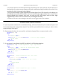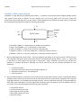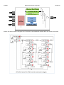
1
The University of Texas at Austin
EE460M Lab Manual
Dept. of Electrical and Computer Engg.
EE 460M
Digital Systems Design Using VHDL
Lab Manual
Table of Contents
ABOUT THE MANUAL
3
LABS AT A GLANCE
4
LAB POLICIES
5
FREQUENTLY ASKED QUESTIONS
6
LAB ASSIGNMENT #0
16
LAB ASSIGNMENT #1
18
LAB ASSIGNMENT #2
21
LAB ASSIGNMENT #3
27
LAB ASSIGNMENT #4
5
LAB ASSIGNMENT #5
4
LAB ASSIGNMENT #6A
13
LAB ASSIGNMENT #6B
21
LAB ASSIGNMENT #7A
25
LAB ASSIGNMENT #7B
37
EE 460M
Digital Systems Design Using VHDL
Lab Manual
About the manual
This document was created by consolidation of the various lab documents being used for EE460M
(Digital Design using VHDL). It is intended to serve as a lab manual for students enrolled in EE460M at
the University of Texas at Austin.
The creation process started towards the end of Spring 2011 and was accomplished by Aman Arora
(TA, EE460M) under the guidance of Prof. Lizy John. In its present form, this document includes
several changes (additions, deletions and modifications) incorporated over three semesters – Spring
2011, Fall 2011 and Spring 2012.
Several important modifications include:
1. Re-organization of Lab#1 and Lab#2 to remove several unimportant and quaint problems
2. Consolidation of tutorials which were spread over Lab#1 and Lab#2 into Lab#0
3. Addition of Lab#6B, which caters to design for test (DFT) concepts
4. Changes in values/design parameters in various labs
5. Re-organization of Lab#5 into three parts
6. Introducing ChipScope
7. Adding the ARM processor lab and the bowling score keeper lab in the appendix
8. Addition of several important details to improve clarity
a. Mostly answers to students doubts
b. Several diagrams
c. Additional explanations
This document is currently maintained by Aman Arora. He can be contacted through email at
[email protected]. Please write to him in case of any questions or concerns or suggestions.
Important: Do not print this entire document. This document will be updated during the semester.
EE 460M
Digital Systems Design Using VHDL
Lab Manual
Labs at a glance
S.No.
Brief Description
Objective
Duration
Points Possible
0
Tutorials – ModelSim and
Xilinx ISE & ChipScope and
Nexys2 Board
Introduction to digital design using
FPGAs. Introduction to simulation
and synthesis.
1 week
50
1
Subtractor and ALU
Simple combinational circuit design
1 week
100
(40+40+20)
2
Excess-3 code converter and
BCD counter
Simple sequential circuit design
1 week
100
(40+30+30)
3
Package sorter and
Traffic Light Controller
More digital design. Introduction to
testbenches.
1.5 weeks
120
(20+50+50)
4
Parking Meter
Advanced digital design. Interfacing
with 7-segment display and push
buttons.
2 weeks
150
5
A basic SNAKE game
Interfacing with PS/2 Keyboard and
VGA display
2 weeks
180
(50+50+80)
6a
Stack Calculator
Using Block RAMs on FPGAs
1 week
100
6b
Memory BIST
Understanding JTAG and BIST
1 week
100
7a
MIPS Processor
TEXTIO in VHDL
1 week
100
7b
MIPS Processor extension
Basic microprocessor design
1 week
100
Important: Please check the schedule sheet on Blackboard for the lab due dates
EE 460M
Digital Systems Design Using VHDL
Lab Manual
Lab Policies
1. You will (have access to and) work in the lab in ENS 302. This is also where TA office hours will be held.
2. This document, available on Blackboard, will serve as the lab manual for the entire semester. The
document contains all the lab information you need to do the labs (except for few codes in labs 6 and 7).
You can work on your own pace throughout the semester, but you have to follow the due dates for
submission (listed in the schedule document) and the check out procedures.
3. All communication will be done through Blackboard. So, please keep checking Blackboard for notifications
and updates. Important information will also be emailed.
4. 15-minute lab discussion sessions will be held at appropriate dates (listed in the schedule document)
before the lecture. These will be conducted by the TAs. It is advisable to read about that lab from the lab
manual before coming to the class, so that you are better prepared to ask questions and resolve doubts.
5. Labs 0, 1 and 2 are to be done individually. Labs 3 through 7 can be done in groups of two. Also, working in
groups does not mean that you work on separate parts of the lab. Both the group members are supposed
to know and answer questions about all parts of the lab. You can switch partners whenever you want.
6. Grading will occur in two parts: submission and demo (checkout).
7. For submission, upload all relevant files (specified with each lab under the ‘Submission Details’ section) via
Blackboard. One of the members from each group should log into Blackboard and go to “Labs/Submission”
section and then upload all the necessary files under the appropriate link.
8. Lab due dates (submission dates) are specified in the course schedule document on Blackboard.
9. After you submit your files, you have to demonstrate your designs to one of the TA’s in the ENS 302 lab.
Once the lab is submitted, DO NOT make changes! You must demo with the code you submitted. In the
event you decide to change the code for the demo, the day of the demo will be considered the turn-in
date, and the appropriate late penalty will be applied.
10. A checkout sign-up sheet is available on Blackboard. After every lab due date, the TAs will email the class
to sign-up for a checkout slot. Put your name in that sign-up sheet and reserve a time-slot for your check
out. Please reach the lab atleast 5 minutes before your slot. In case of group labs (lab 3 and above), only
one member of the group should submit the files but both members of a group must checkout together.
So, the entries in the checkout slot registration sheet should contain two names.
11. In case you miss your check out slot, you can check out for that lab during office hours anytime before the
next lab’s due date. In other words, the TA’s will not entertain requests for checking out labs older than
the previous lab.
12. The possible points for each lab are mentioned in the ‘Labs at a glance’ section of this manual. Late
submissions (not late checkouts) will lead to penalty according to the following rules:
a. One day late submission – less 10% of your normal score
b. Two day late submission – less 20% of your normal score
c. Three day late submission – less 30% of your normal score
Submissions late by more than 3 days will not be accepted and you will be marked zero (unless you have
taken permission from the professor).
13. Sundays are not counted for late submissions. So, if a lab is due on Saturday and you submit it on Monday,
it
will
be
considered
1-day
late
submission.
EE 460M
Digital Systems Design Using VHDL
Lab Manual
Frequently Asked Questions
MODELSIM
Q. In ModelSim 6, when I click the message saying x errors in the transcript window, the window that pops
up does not show me any errors?
This is because you file name (complete path) has spaces in it. While using ModelSim, please make sure that
the file name doesn't have any white spaces. In other words, do not have your programs saved on a path like
"xyz\Documents and Settings\user1\lab 1\file.vhd". Please make a folder on the C: drive of the computer you
work on and keep your project/source files there.
Q. When I click on ModelSim, it gives me an error saying failed to checkout license.
In case invoking ModelSim shows a licensing error on the lab computers, please run the Licensing Wizard first
(Start->Programs->ModelSim->Licensing Wizard), and then launch ModelSim.
Q. How do I create and run a do-file?
The ModelSim tutorial talks about creating a file of commands in the end (called a do-file), but does not
explain how to do it clearly. Here is how you can do this: Basically, the commands like force, run, etc that you
provide on the transcript window can be saved in a file and that file is called a "do-file". The benefit of having
a do-file is to be able to re-run all the commands by just a single click, rather than typing them again and
again. For example, if you have your do-file ready during the checkout, you can just execute it instead of
typing the individual commands all over again.
There are two ways of creating a do-file.
1. You can manually write those commands in a file using a text editor and save it with a ".do" extension.
2. You can type the commands on the transcript window, and then have ModelSim create the file for you.
For this, type the commands in the transcript window (keep the transcript window selected). Then go
to "File->Save As", and then provide the name of the file with a .do extension.
To execute the commands in the do-file, make sure the transcript window is active. Then, go to "File -> Load"
and then provide your do-file to the tool.
Q. Can I view variables on waveforms?
Viewing variables on the waves is just like viewing signals (of course, you should be simulating your design to
view the waves). The ‘Objects’ window shows you the signals in a design. Similarly, the “Locals” window shows
the variables in the selected entity/process. For seeing variables, go to the ‘View’ menu and click on ‘Locals’. A
‘Locals’ window will appear.
When you are simulating, you can see that a “Sim” pane appears near to your “Project” and “Library” panes.
Click on the “Sim” pane and it will show you the design hierarchy. You can click on any entity or a line number
of a process statement whose variables you want to see. Now, in the “Locals” window, you can click on
variables and then drag to the waveform window.
EE 460M
Digital Systems Design Using VHDL
Lab Manual
Q. Some signals in my design are not visible in the “Objects” window, and so I can’t view their waveforms.
This is because ModelSim performs a series of optimizations on your design and can get rid of some signals.
The ‘optimized out’ signals can not be seen in the “Objects” window. You can disable optimization in two
ways:
1. While starting simulation, instead of just double clicking on the entity name in the “Library” window,
right click and say “Simulate without Optimization”.
2. On the transcript window, append “ –novopt” to the “vsim” command
Q. Can I view waveforms of signals inside the design hierarchy (entities other than the top module)
When you are simulating a design, you can see that a “Sim” pane appears near to your “Project” and “Library”
panes. Click on the “Sim” pane and it will show you the design hierarchy. You can click on any entity in the
design. When you click on an entity, the “Objects” window shows the signals in that entity. Now, in the
“Objects” window, you can click on signals and then drag to the waveform window (or you can right click a
signal and say Add->To Wave->Selected Signals).
Q. How can I change the way signals are shown on the waveforms (To change viewing 000101 to 5)
Right on the signal in the “Waves” window, got to “Radix” and select the one you want.
Q. How can I create a clock using the force statements in ModelSim during simulation?
To create/generate a clock, you can use the following command:
force clk 0 0 ns, 1 10 ns –repeat 20 ns
This command creates a clock of period 20 ns with 50% duty cycle as shown below:
0ns
10ns
20ns
30ns
40ns
You can change the period and duty cycle as you want by modifying the force statement appropriately.
Q. I used the ‘force’ command to force a signal. Now I want the design to drive it. But it is just stuck to that
value.
A force statement forces the specified value onto the specified signal at the specified time and then that value
remains on that signal for the entire simulation. It can only be changed by another force statement.
Adding "-deposit" option to the "force" command puts the specified value on the specified signal at the
specified time, but lets it change anytime after that (if another driver wants to modify/override it; for example
an assignment statement in the design).
For example, let’s assume that you have an output that you want to initialize to 0 at the beginning of the
simulation. Assuming also that you have not initialized this output to 0 in your code, you may simply type:
force Z 0 0 ns. You will note after running the simulation that Z never changes. To overcome this problem,
change the above statement to: force –deposit Z 0 0 ns. The deposit will simply deposit the value of 0 to Z at
0ns instead of freezing it at 0.
The "-cancel" option cancels the force on a signal at a specified time.
EE 460M
Digital Systems Design Using VHDL
Lab Manual
You can look into more options of the force statement by going to "Help -> PDF Documentation -> Reference
Manual" in ModelSim.
Q. ModelSim 10 is showing me errors if I use the code from the book.
The code from the book has been tested on ModelSim 6. There might be some code snippets which don’t
work in ModelSim 10. So far, the following issues have been observed. The following codes won’t work in
ModelSim 10:
1. Output <= A(2 downto 0) & A(3);
where Output and A are unsigned(3 downto 0)
Instead use the rol/ror operators, or switch to ModelSim 6
2. Output <= A(2 downto 0) & '0'
Instead use Output <= A(2 downto 0) & "0", or switch to ModelSim 6
XILINX ISE
Q. Xilinx ISE is so slow! What should I do?
It is recommended, in general, to work on files in the local directories (C: drive, for example) while working
with Xilinx ISE and ModelSim in the lab. Your desktop is a networked drive and these tools work really slow
when they have to fetch files over the network. But since the files in local directories get cleaned up when you
log out, make sure you make a copy somewhere before you logout.
Q. What is a UCF File? Can I hand write it instead of using the PACE window?
The UCF file is the file which tells Xilinx ISE to map the inputs and outputs of your design to specific pins on the
FPGA. The file also has other things like clock constraints etc, but we are not going to be concerned about
them in this lab. The PACE tool helps you graphically create the UCF file. However, you can manually write a
UCF file too (it is just a text file with a specific format). This may sometime be required if the PACE tool does
not work. Assuming the the PACE tool works in your first lab, to view the UCF generated by it, click on the UCF
filename in the Design Hierarchy panel. Now, in the processes panel, expand ‘User Constraints’ by clicking on
the ‘+’ sign. Now double click, ‘Edit Constraints’. This will open the UCF file in the right hand side of the
window. The syntax is self-explanatory. So, if PACE doesn’t work in any lab, open the UCF from a previous
project, copy it to the current project and modify it manually for the current project’s constraints.
EE 460M
Digital Systems Design Using VHDL
Lab Manual
VHDL
Q. Can I model combinational logic using process statements? How?
Ideally, concurrent statements are used to model combinational logic and process statements are used to
model sequential logic (flip flops and latches). However, process statements are not restricted to that. You can
model combinational logic using them. But it is important to note that when using a process statement to
make combinational logic, the sensitivity list of the process statement should contain all the signals which are
being ‘read’ in that process. In other words, to synthesize combinational logic using a process, all inputs must
appear in the sensitivity list.
For example, if you were to model a mux, you would say:
process(a,b,sel)
begin
if sel = 1 then z <= a;
else
z <=b;
end if;
end process;
Using a process statement to model combinational logic is handy because statements like if, case, etc (which
are very useful and intuitive) can only be written inside process statements.
Q. What care should I take when using the process statement to write sequential logic?
When using a process statement to model sequential logic, the only thing in the sensitivity list of the process
statement should be the clock (or a reset signal, if it is an asynchronous reset). And there should be an ‘if’
statement inside the process which has clk=’0’ (clk=’1’) and clk’event. This is because flip-flops are edge
triggered elements.
Flip-flop without a reset
process(clk)
begin
if clk = ‘1’ and clk’event then
q <= d;
end if;
end process;
--positive edge triggered
Flip-flop with an async reset
process(clk, rst)
begin
if rst = ‘0’ then
--active low reset
q <= ‘0’;
elsif clk = ‘1’ and clk’event then --positive edge triggered
q <= d;
end if;
end process;
Flip-flop with a sync reset
process(clk)
begin
if clk = ‘0’ and clk’event then --negative edge triggered
if rst = ‘1’ then --active high reset
q <= ‘0’;
EE 460M
Digital Systems Design Using VHDL
Lab Manual
else
q <= d;
end if;
end if;
end process;
On the other hand, a latch is a level triggered element. A resettable latch can be modeled as:
process(en, rst, d)
begin
if (rst = ‘0’) then
q <= ‘0’;
elsif (en = ‘1’) then
q <= d;
end if;
end process;
Q. Why can I not use a ‘port map’ statement inside an ‘if’ statement (or a process statement, for that
matter)?
It is important to realize that a ‘port map’ statement is not like ‘calling’ a function in C. It is an instantiation of
an entity. Therefore, it cannot be conditional. If you have to instantiate a block in your design, it will be always
present there.
Let us take an example. Say you have an adder and a subtractor. You design’s specifications say that when the
input MODE is ‘1’, the design should work as an adder, while when the MODE is ‘0’, the design should work as
an subtractor. Now, this does not mean that you can have something like this:
process(…)
if(MODE = ‘1’) then
adder_inst: adder port map (…);
else
subt_inst: subtractor port map (…);
end if;
end process;
Since we are modeling hardware, we cannot say that if MODE is 1, Adder is ‘called’ and when MODE is 0,
subtractor is ‘called’. This is a wrong way of thinking.
Instead you should think of this as: Adder and Subtractor are always present. The output of the design can be
driven by either the Adder or the Subtractor depending on MODE. So you should have something like this:
adder_inst: adder port map (…,add_out);
subt_inst: subtractor port map (…,sub_out);
process(…)
if(MODE = ‘1’) then
output <= adder_out;
else
output <= sub_out;
end if;
end process;
EE 460M
Digital Systems Design Using VHDL
Lab Manual
GENERAL
Q. What tests should the ‘do’ file that I submit on blackboard contain?
It is always better to submit a do-file which has sufficient number of input combinations (not just the ones
given in the lab description).
Q. I am getting a multiple drivers error. What should I do?
A multiple driver error is because there is more than one thing driving a signal. This can happen if you are
driving a signal from two sources: like one process statement and one concurrent statement, or two process
statements. Realistically, it is not possible to do so (without having contention, which we are staying away
from). There is nothing you can do to get rid of this, other than changing your design.
Q. My design compiles successfully in ModelSim. When I simulate, I get weird errors (like entity not bound,
error loading design, etc) and I can’t simulate.
The compilation process looks at individual modules (entity-architecture pairs) in your design and checks for
syntactical and semantic correctness. Simulation lets you apply inputs and observe outputs. Between
compilation and simulation, is a step called elaboration (which is usually hidden from you, and happens when
you start simulation in ModelSim). During this step the design hierarchy is generated. Connections between
various entities, matches between entity and component declarations, search for entities referenced as
components in a design, etc are done at this stage. If there is a problem at this stage (for example, there is a
component declaration in your top module but the entity-architecture pair for that component is missing),
they are reported just before simulation. So, now you know where to look for when you get errors just when
you start simulation.
Q. Will setup and hold time be met in my simulation? Or If I add some logic between two stages in my
design, will the delay affect the output? Or should I force my input sometime before the clock edge to
satisfy setup and hold time constraints?
Remember that the simulations that you are doing in the lab are all RTL simulations. They are zero-delay
simulations (assuming you are not modeling delays using ‘after’ statements). Therefore, there is no concept of
delays of gates or setup-hold time of flip-flops. If we were doing post-synthesis simulations, then we would
have concerned timing issues.
Q. I have “library ieee; use ieee.numeric_bit.all” written at the top of my file. But I am still getting errors like
‘unsigned is not a recognized type’, etc.
This error should not pop up if there is just one entity-architecture pair in a VHDL file. The ‘library’ and ‘use’
statements have to be written separate for each entity-architecture pair you have in a file. So, if you have
multiple entity-architecture pairs in a single file, use the ‘library’ and ‘use’ statements before each entity.
EE 460M
Digital Systems Design Using VHDL
Lab Manual
GOOD DESIGN PRACTISES
Q. Are there any general ‘good’ design practices that I should follow?
1. Writing VHDL feels like writing software. But it is a good idea to think ‘hardware’ while writing code!
2. Do not use ‘after’ statements in your designs in the lab. Testbenches may use these. Eg. To generate a
clock signal in a testbench you can say “clk <= not clk after 20 ns;”
3. A state machine can be designed using either a single process statement (like Figure 2.56 in the text) or
using two process statements (like Figure 2.54 in the text). Both ways are correct. However, it is easier
to design it using a single process statement. Generally, the single process statement partakes less
debugging effort.
4. Stay away from ‘variables’ unless you are absolutely sure.
5. Concurrent statements are continuous drivers. Do not use them for initializations.
6. It is a good idea to have a reset signal in your design (even if not mentioned in the lab description). Use
this signal to reset all the things you want to. Do not rely on the initialization statements (like signal a:
bit_vector(3 downto 0) := “0001”;). These are honored in simulation, but may not be honored in
synthesis.
7. While simulating your design, it is always a good idea to stagger your inputs with respect to the active
clock edge. For example, if your active clock edge is occurring at 10ns, apply your inputs sometime
before 10ns, say at 8ns. This ensures that when your design was clocked, the input was successfully
read. If your active edge occurs at 10ns and your input also changes at 10ns, then it becomes hard to
see whether the input was successfully captured by the clock edge or not. Debugging becomes harder
if you have your inputs like that.
8. Don’t limit your testing to the input sequences mentioned with the problem statement. During the
checkouts, the TAs will apply several input combinations to test your design. So, make sure to do a
thorough testing of your design using sufficient number of inputs.
9. Generally, we tend to ignore warnings from the tools. But make sure you look at all the warnings after
the synthesis process is completed. Sometimes there are problems in your design like missing
connections, latches, etc. Such issues make the tool infer your design differently from what you want
or expect it to be. These warnings might contain the reason why your design does not work on the
board.
Q. My design works in simulation. But it does not work on the board. What should I do?
There is no one sentence answer to this question. You can try the following things to help you debug your
problem:
1. Follow the good design principles discussed above.
2. Look for any warnings in the synthesis report.
3. Make sure there are no latches in the synthesized output.
4. Use ChipScope to perform in-circuit debug.
5. Follow the synthesis-friendly code guidelines discussed in the next question
Q. My design works in simulation. But Xilinx ISE throws an error during synthesis, saying “Bad Synchronous
Description”. What am I doing wrong?
The one line answer to this question is that you are not writing synthesizable code. Here are a few tips:
1. 'event should only be used on clocks
EE 460M
Digital Systems Design Using VHDL
Lab Manual
2. a process statement to model sequential logic should only have clock (and reset, if you need one) in
the sensitivity list, and a process statement to model combinational logic should not have clock in the
sensitivity list. (this is illustrated in detail below)
3. a signal cannot change on both negative and positive edges of clock (This is specific to the design you
do in the lab because the FPGA hardware does not have dual edge triggered flops. This is true for most
industrial design also. However, there may be some very high end designs which use dual edge
triggered flops, in which case this constraint on your code gets removed.)
4. make sure the tool is able to decipher the value of each signal under each condition.
Synthesis friendly ‘process’ statements
A. If you use process statement for a combinational logic, make sure the sensitivity list contains all inputs. And
the clock should not be amongst those inputs! If you feel like you need the clock, it means you want to write
sequential logic. Think again!
B. All processes other than the ones used for combinational logic will have a structure similar to this:
process(clk, rst)
begin
if rst = ‘0’ then
--initializations
elsif clk = ‘1’ and clk’event then
--actual stuff
end if;
end process;
--positive edge triggered
C. So, any process in your design should fall into either of the following categories:
process(clk, rst) --model sequential logic -async reset
begin
if rst = ‘0’ then --this is for asynchronous reset
--initializations
elsif clk = ‘1’ and clk’event then
--actual stuff
end if;
end process;
process(clk) --model sequential logic -sync reset
begin
if clk = ‘1’ and clk’event then
if (rst = ‘0’) then --this is for sync. reset
--initializations
else
--actual stuff
end if;
end if;
end process;
process(clk) --model sequential logic -no reset
begin
if clk = ‘1’ and clk’event then
--actual stuff
end if;
end process;
EE 460M
Digital Systems Design Using VHDL
process(a,b,c)
begin
--logic
end process;
Lab Manual
--model combo logic --donot have clock in the list
Q. Xiinx ISE reports there are latches in my design. Where am I going wrong?
Latches are caused when you forget an ‘else’ block in an ‘if’ or ‘case’ statement in a process statement
intended to make combinational logic. Look at your design and find such cases.
Example:
The following process statement was intended to make do some selection. It was expected that a mux will be
generated for both f and g.
process (sel, a, b, c, d)
begin
case sel is
when 000 =>
f <= a; g <= c;
when 001 =>
f <= b; g <= d;
when 010 =>
f <= a; g <= c;
when 011 =>
f <= b;
when 101 =>
f <= a; g <= b;
when 110 =>
f <= b; g <= d;
when 111 =>
f <= a; g <= b;
end case;
end process;
But notice that the assignment to ‘g’ was missed in one case. And one case (100) was not mentioned.
Therefore, latches were inferred for both ‘g’ and ‘f’. Here is the correct way to write this:
process (sel, a, b,
begin
case sel is
when 000 =>
f
when 001 =>
f
when 010 =>
f
when 011 =>
f
when 101 =>
f
when 110 =>
f
when 111 =>
f
when others =>
end case;
end process;
c, d)
<= a; g
<= b; g
<= a; g
<= b; g
<= a; g
<= b; g
<= a; g
f <= a;
<= c;
<= d;
<= c;
<= d;
<= b;
<= d;
<= b;
g <= d;
Also, in a process statement used to model combinational logic, if you forget to assign all signals under all
conditions, you will end up with latches. So, to synthesize combinational logic using a process statement, all
signals must be assigned under all conditions.
Example:
process (state, a, b, c, d, e)
begin
case state is
when IDLE =>
if a = '0' then
next_state <= INITIAL;
end if;
when INITIAL =>
EE 460M
Digital Systems Design Using VHDL
Lab Manual
if a = '1' then
next_state <= ERROR_FLAG;
else
next_state <= SCANNING;
end if;
Since ‘next_state’ is not assigned when a is ‘1’, a latch is inferred. To avoid unwanted latches, a good way is to
make sure you assign all signal under all possible conditions.
process (state, a, b, c, d, e)
begin
case state is
when IDLE =>
if a = '0' then
next_state <= INITIAL;
else
next_state <= IDLE;
end if;
when INITIAL =>
if a = '1' then
next_state <= ERROR_FLAG;
else
next_state <= SCANNING;
end if;
But an easier (sometimes; depends on functionality) way can be to create a default assignment for all the
variables in the process.
process (state, a, b, c, d, e)
begin
--default assignment
next_state <= IDLE;
case state is
when IDLE =>
if a = '0' then
next_state <= INITIAL;
end if;
when INITIAL =>
if a = '1' then
next_state <= ERROR_FLAG;
else
next_state <= SCANNING;
end if;
EE 460M
Digital Systems Design Using VHDL
Lab Manual
Lab Assignment #0
This lab is a tutorial lab. You don’t have to design anything in this lab, just go through the tutorials and
perform them on the lab computers individually. In this course, in almost all the labs we will be doing the
following steps:
Step 1: Writing VHDL code of the circuit we want to implement
Step 2: Simulating the VHDL code using a simulator (ModelSim) to check if the intended functionality has been
achieved
Step 3: Synthesizing the VHDL code using a tool form Xilinx called ISE so that it can be programmed onto an
FPGA
Step 4: Programming the FPGA (a Spartan3E series FPGA from Xilinx) on the lab board (called Nexys2 board)
using a tool called Adept
Step 5: Applying inputs to and observing outputs from our circuit using the peripherals (like switches, buttons,
LEDs, etc) on the Nexys2 board
To be able to do all this, we need to learn how to use ModelSim and Xilinx ISE tools, and we also need to
understand the capabilities of the Nexys2 board and how can we program the Xilinx Spartan3E FPGA on it
using Adept. The following activities will help you go through all the steps so you can learn and use the
concepts in the upcoming labs.
Activity 1: ModelSim tutorial
Mentor Graphic’s Modelsim tool will be used to perform the functional simulation of our VHDL code for the
course. This software is available in all of the ENS labs. Modelsim is also available as a free download with
Xilinx’s Webpack software so you can install it on your own computer..
Go through the “Modelsim Tutorial” posted on Blackboard under “Course/Labs/Lab Info”. This tutorial goes
through the basic steps in compiling and simulating within the Modelsim environment using a simple D-flipflop
as an example.
Activity 2: Xilinx ISE tutorial
The XILINX ISE tool is used to synthesize circuits and place & route them for a particular FPGA. Then, a BIT file
needs to be generated (we use the Digilent Adept tool for that) which can be programmed onto the FPGA so
that the FPGA now contains the circuit you designed. Go over the XILINX tutorial that has been posted on
Blackboard. You may also visit www.xilinx.com and browse the Spartan 3e manuals for help.
Go through the “Xilinx ISE tutorial” posted on Blackboard under “Course/Labs/Lab Info”.
Activity 3: Nexys2 board tutorial
Read through the Nexys2 Board User Manual on Blackboard under “Course/Labs/Lab Info” to understand the
features and capabilities of the board to be used in all the labs. Then go through Nexys2 Board Configuration
manual under “Course/Assignments/Lab Info”. This document describes how to program the FPGA on the
board.
EE 460M
Digital Systems Design Using VHDL
Lab Manual
Activity 4: Xilinx ChipScope tutorial
The XILINX ChipScope tool is used for debugging FPGA based designs. It is a software based logic analyzer that
allows monitoring the status of selected signals in a design in order to detect possible design errors. The basic
concept is that you generate some components (called cores) using a tool (called Core Generator), add these
cores to your design, synthesize it and then put it on the board. Then you open up a tool on your computer
(called ChipScope Analyzer) and you can observe the signals of your design on the screen. Which signals you
want to observe is declared when you integrate the cores in your design.
Go through the “Xilinx ChipScope tutorial” posted on Blackboard under “Course/Labs/Lab Info”.
Questions
You should be able to answer (almost all of) the following questions after going through these tutorials:
1.
2.
3.
4.
5.
6.
7.
8.
What is the ModelSim? What is the role of the transcript window which appears on the bottom of the
main ModelSim window?
What is a delta cycle in a VHDL simulator like ModelSim?
How do you create a do-file of commands entered in the transcript window in ModelSim?
Describe the roles and functionality of the following tools in the Xilinx ISE suite: Project Navigator, RTL
schematic viewer, and PACE.
What is the purpose of using the Adept software?
What two devices appear in the Adept programming interface? In what situations might we wish to
program one over the other?
Is it possible to display two digits using the 7SEG LEDs at the same time on the Nexys2 boards? Note
there are only 7 pins corresponding to a single 7-segment digit.
If we want to use the push buttons on the board reliably, what should we do first to the incoming
signal into the FPGA? How do we implement this in VHDL?
Submission and Checkout details
Submit a text/doc/pdf file containing the answers to the questions given above on Blackboard. Name the file
“your_last_name.extension”. You need to demonstrate that you performed the tutorials during the checkout.
Also, you will be asked questions about various aspects covered in the tutorial. Your ability to answer them
and your demonstration will decide your score.
EE 460M
Digital Systems Design Using VHDL
Lab Manual
Lab Assignment #1
Guideline
This lab is to be done individually. Each person does his/her own assignment and turns it in.
Objective
To learn designing basic combinational circuits in VHDL and implementing them on an FPGA.
Problem 1: Subtractor Design
a. Write VHDL code for a 1-bit full subtractor using logic equations (Difference = A-B-Bin). If you use delays, make sure
to simulate for long enough to see the final result.
b. Write VHDL code for a 4-bit subtractor using the module defined in part (a) as a component. If you use delays, make
sure to simulate for long enough to see the final result. Test it for the following input combinations:
1. A = 1001, B = 0011, Bin = 1
2. A = 0011, B = 0110, Bin = 1
Verify that your design works correctly by using the “force” and “run” commands in the transcript window to provide
inputs and observe outputs on the waveform window.
Problem 2: ALU Design
Design an Arithmetic and Logic Unit (ALU) that implements 8 functions as described in Table 1. Table 1 also illustrates
the encoding of the control input.
The 4-bit ALU has the following inputs:
• A: 4-bit input
• B: 4-bit input
• Cin: 1-bit input
• Output: 4-bit output
• Cout: 1-bit output
• Control: 3-bit control input
Control
000
001
010
011
100
101
110
111
Instruction
Add
Sub
Or
And
Shl
Shr
Rol
Ror
Table 1: ALU Instructions
Operation
Output <= A + B + Cin; Cout contains the carry
Output <= A – B - Cin; Cout contains the borrow
Output <= A or B
Output <= A and B
Output <= A(2 downto 0) & ‘0’
Output <= ‘0’ & A(3 downto 1)
Output <= A(2 downto 0) & A(3)
Output <= A(0) & A (3 downto 1)
EE 460M
Digital Systems Design Using VHDL
Lab Manual
The following points should be taken care of:
• Use a case statement (or a similar ‘combinational’ statement) that checks the input combination of “Code” and
acts on A, B, and Cin as described in Table 1.
• The above circuit is completely combinational. The output should change as soon as the code combination or
any of the input changes.
• You can use arithmetic and logical operators to realize your design.
Simulate this circuit by using the “force” and “run” statements in the transcript window to provide inputs and observe
outputs on the waveform window.
Problem 3: Synthesizing and implementing the subtractor on the FPGA
Create a new project in Xilinx ISE. Use the code for the 4-bit subtractor that you wrote in Problem 1. Synthesize and
implement the design on the Spartan3E FPGA on Nexys2 board. Use the following pin assignments for creating the UCF
file:
A
B
Bin
Diff
Bout
Switches[7->4]
Switches[3->0]
BTN0
LED[3->0]
LED4
Download the design onto the board and make sure it works as expected. Include the design_name.bit file that you
download to the board in your Blackboard submission.
Useful Information
1. For problem 2, you can use the subtractor block from problem 1 for doing the subtraction (although just
using the arithmetic operators will make your design easier). If you use the subtractor from problem 1,
remember that we are designing hardware. So, doing something like the following is incorrect:
architecture xyz of abc is
process(…)
case control is
when “001” => sub_inst : four_bit_sub port map (in1,in2,bin,output);
……
First of all, it is important to realize that a ‘port map’ statement is not like ‘calling’ a function in C. It is an
instantiation of an entity. Therefore, it cannot be conditional. It is always present. So, you sould do
something like this:
architecture xyz of abc is
sub_inst : four_bit_sub port map (in1,in2,bin,sub_out)
process(…)
case control is
when “001” => output <= sub_out
EE 460M
Digital Systems Design Using VHDL
Lab Manual
……
Adder
add_out
Subtractor
sub_out
output
Inputs
(A,B,Cin)
Logic
.
.
Logic
2. Make sure that your designs work by testing them sufficiently thoroughly. You should not just use the test
inputs in the lab description. Also, it is always better to submit a do-file which has sufficient number of input
combinations (not just the ones given in the lab description).
3. Do not use ‘after’ statements in your design for providing delays in your design.
X <= A or B after 15 ns;
In fact, you should never use the ‘after’ statement in the lab during the semester.
Submission Details
All parts of this lab will be submitted on Blackboard only. You will not need to submit anything as a hard copy. For each
problem, please zip all relevant files into a single folder with the following naming scheme: Lastname_Problem#.zip
Problem
1
2
3
Submission Requirements
• VHDL file(s)
• Do-file
• VHDL file(s)
• Do-file
• Bit-file
• UCF File
Checkout Details
You will be expected to describe briefly the codes for problems 1 and 2, simulate and show waveforms in Modelsim, and
answer verbal questions. Also, for the last problem you will have to demonstrate that your circuit works on the board.
EE 460M
Digital Systems Design Using VHDL
Lab Manual
Lab Assignment #2
Guideline
This lab is to be done individually. Each person does his/her own assignment and turns it in.
Objective
To learn designing basic sequential circuits in VHDL and implementing them on an FPGA.
Problem 1: Excess-3 code converter design
In this problem, you will be designing an FSM using three different styles of VHDL coding: behavioral, dataflow, and
structural. The following is the problem for which you will be designing the FSM:
A sequential circuit has one input (X), a clock input (CLK), and two outputs (S and V). X, S and V are all one-bit signals. X
represents a 4-bit binary number N, which is input least significant bit first. S represents a 4-bit binary number equal to
N + 3, which is output least significant bit first. At the time the fourth input occurs, V = 1 if N + 3 is too large to be
represented by 4 bits; otherwise, V = 0. The value of S should be the proper value, not a don’t care, in both cases. The
circuit always resets after the fourth bit of X is received. Assume the sequential circuit is implemented with the following
state table. The outputs are (S,V). All state changes occur on the falling edge of the clock pulse.
Present State
S0
S1
S2
S3
S4
S5
S6
Next State
X=0
X=1
S1
S2
S3
S4
S4
S4
S5
S5
S5
S6
S0
S0
S0
S0
Output
X=0
X=1
1,0
0,0
1,0
0,0
0,0
1,0
0,0
1,0
1,0
0,0
0,0
1,0
1,0
0,1
a. Write a behavioral VHDL description using the state table shown above. Compile and simulate your code using the
following test sequence:
X = 1011 1100 1101 The first input bit is at the far right. This is the LSB of the first 4-bit value. Therefore, you will be adding 3 to 13, then
to 12, and then to 11. While simulating, keep the period of the CLK to be 10ns. Change X 1/4 clock period after the
rising edge of the clock.
b. Write a data flow VHDL description using the next state and output equations to describe the state machine. You
can use Logic Aid to derive the logic equations. Assume the following state assignment:
S0 = 000, S1 = 010, S2 = 001, S3 = 101, S4 = 011, S5 = 100, S6=111
Compile and simulate your code using the same test sequence and timing as (a).
c. Write a structural model of the state machine in VHDL that contains the interconnection of gates and D flip-flops.
Compile and simulate your code using the same test sequence and timing as (a).
EE 460M
Digital Systems Design Using VHDL
Lab Manual
Problem 2: BCD Counter Design
Implement a 1 digit BCD (binary coded decimal) counter. It should be a synchronous (4-bit) up/down decade counter
with output Q that works as follows: All state changes occur on the rising edge of the CLK input, except the
asynchronous clear (CLR). When CLR = 0, the counter is reset regardless of the values of the other inputs. You can keep
the time period of the CLK signal to 10ns for simulating your design.
D
CO
BCD Counter
ENABLE
LOAD
UP
CLR
Q
If the LOAD = ENABLE = 1, the data input D is loaded into the counter.
If LOAD = 0 and ENABLE = UP = 1, the counter is incremented.
If LOAD = 0, ENABLE = 1, and UP = 0, the counter is decremented.
If ENABLE = 1 and UP = 1, the carry output (CO) = 1 when the counter’s value is 9.
If ENABLE = 1 and UP = 0, the carry output (CO) = 1 when the counter’s value is 0.
a. Write a VHDL description of the counter. You may implement your design in any style you wish. It will be easier to
use a behavioral description which can be either written in the algorithmic way (eg. Count <= Count + 1 – Figure 2.46
in the text) or a state machine way (eg. State <= Next_State – Figure 2.54/2.56 in the text). You may also use
dataflow or structural descriptions, although that will be more work. Use the following simulation for your
waveforms:
1.
2.
3.
4.
Load counter with 6
Increment counter four times. You should get 9 and then 0.
Decrement counter once. You should get 9.
Clear the counter.
b. Write a VHDL description of a decimal counter that uses two of the above counters to form a two-decade decimal
up/down counter that counts up from 00 to 99 or down from 99 to 00. In other words, instantiate (port map) two
single digit counters in a top module (the two-digit counter). You may need some extra logic in the top module too
other than these instantiations. The top module will have these inputs and outputs: CLR, CLK, ENABLE, LOAD, UP,
D1, D2, Q1, D2, CO. Use the following simulation for your waveforms:
1. Load counter with 97
2. Increment counter five times.
3. Do nothing for 2 clock periods
3. Decrement counter four times.
4. Clear the counter.
EE 460M
Digital Systems Design Using VHDL
Lab Manual
Problem 3: Synthesizing and implementing the BCD counter on the FPGA
Use the code for the single digit BCD counter that you wrote in Problem 2a. Before you synthesize it and implement it on
the board, you will have to modify your code a little bit. This is because the CLK signal available on the board is a high
frequency signal (50 MHz). If you use this high frequency for your circuit, you will not be able to give proper inputs or
see proper outputs to your design.
So, you need to add a clock divider to your VHDL description. Create two more entities in your design. Call one as top
and another as divider. Make connections as shown in the following figure. Look at the codes given in the end of this
document, understand them and see how they can be used as clock dividers.
Ensure that there are no latches in your design. Xilinx ISE will report these in the Synthesis report. You need to eliminate
such warnings. You may want to read the synthesis guidelines “Tips for writing synthesizable code” available on
Blackboard.
To look for latches in your synthesized design, open the synthesis report generated by ISE by clicking “View Synthesis
Report” under the “Synthesize-XST” option. In the synthesis report, look for “Macro Statistics” and see if any latches are
being shown. Alternatively, you can look for “cell usage” in the report and there should not be any cells under “Flip
Flops/Latches” having names starting with “L”.
Also, after adding the counter/clock divider block to your design, simulate the top entity in Modelsim before directly
synthesizing using ISE to ensure that the counter/divider works. And while simulating, reduce the large values (like
5000000) in the counter to small values (say 50), so that simulation takes less time and the waveforms are legible. Don't
forget to switch to the correct (large) value before synthesizing.
TOP
CLK
input
(connect it
to 50MHz
clock –
B8)
Divider
Slow
clock
BCD
Counter
Outputs
Other
inputs
Synthesize the top module (which includes the divider and the 1-digit bcd counter) and use the following pin
assignments. Download the design onto the board and make sure it works as expected.
LOAD
D
ENABLE
UP
CLK
COUNT
CO
BTN0
SW[3:0]
SW4
SW5
B8
LED[3:0]
LED4
EE 460M
Digital Systems Design Using VHDL
CLR
Lab Manual
SW6
Useful Information
1. Don’t limit your testing to the input sequences mentioned with the problem statement. During the checkouts,
the TAs will apply several input combinations to test your design. So, make sure to do a thorough testing of your
design using sufficient number of inputs.
2. While simulating your design, it is always a good idea to stagger your inputs with respect to the active clock
edge. For example, if your active clock edge is occurring at 10ns, apply your inputs sometime before 10ns, say at
8ns. This ensures that when your design was clocked, the input was successfully read. If your active edge occurs
at 10ns and your input also changes at 10ns, then it becomes hard to see whether the input was successfully
captured by the clock edge or not.
Force inputs here
0ns
10ns
20ns
30ns
40ns
3. A state machine can be designed using either a single process statement (like Figure 2.56 in the text) or using
two process statements (like Figure 2.54 in the text). Both ways are correct. However, it is easier to design it
using a single process statement. Generally, the single process statement partakes less debugging effort. This is
good guideline to observe during the entire semester.
Submission Details
All parts of this lab are to be submitted on Blackboard. No hard-copy submission is needed. For each problem, please zip
all your files into a single folder with the following naming scheme: Lastname_Problem#.zip
Problem
1
2
3
Submission Requirements
• VHDL file(s)
• Do-file
• VHDL file(s)
• Do-file
• VHDL file(s)
• Bit-file and UCF File
Checkout Details
During your checkout you will be expected to demonstrate each of the problems in the assignment and answer verbal
questions about the assignment.
EE 460M
Digital Systems Design Using VHDL
Example 1
library IEEE;
use IEEE.numeric_bit.ALL;
entity simpleCounter is
Port ( clk50Mhz : in bit;
led : out bit);
end simpleCounter;
architecture Behavioral of simpleCounter is
signal counter: unsigned (26 downto 0);
signal cnt_temp: bit_vector(26 downto 0);
begin
process (clk50Mhz)
begin
if clk50MHZ = '1' and clk50Mhz'event then
counter <= counter + 1;
--increment counter every 20 ns (1/ 50 Mhz) cycle.
end if;
end process;
cnt_temp <= bit_vector(counter);
led <= cnt_temp(26);
-- (2^26 / 50E6) = 1.34 seconds
end Behavioral;
Example 2
library IEEE;
use IEEE.numeric_bit.ALL;
entity complex is
Port ( clk50Mhz : in bit;
led : inout bit
);
end complex;
architecture Behavioral of complex is
signal counter: integer range 1 to 50000000;
begin
process (clk50Mhz)
begin
if clk50MHZ = '1' and clk50Mhz'event then
if counter = 50000000 then counter <= 1; led <= not led;
else counter <= counter + 1;
end if;
end if;
Lab Manual
EE 460M
end process;
end Behavioral;
Digital Systems Design Using VHDL
Lab Manual
EE 460M
Digital Systems Design Using VHDL
Lab Manual
Lab Assignment #3
Guideline
This lab can be done with a partner. In fact, partnership is encouraged.
Objective
1.
2.
3.
4.
Understanding the ASIC/FPGA design flow
More digital design - sequential and combinational circuits.
Learn writing and using testbenches in VHDL
Implementing circuits on FPGA
Problem 1: ASIC/FPGA Design Flow
The following figure shows the design flow as described in chapter 2 of the text. Annotate each box in this figure with
the answers to the following questions:
a. What is the function of each box (answer in one line)?
b. Which tool do you use in the lab to perform this step? If a step is not performed in the lab, mark it.
c. What inputs are needed at each stage and what outputs are delivered at each stage?
EE 460M
Digital Systems Design Using VHDL
Lab Manual
Problem 2: Package Sorter (simulation only – using a testbench)
Design a package sorter to classify packages based on their weights and to keep track of packages of different
categories. The sorter has an active high asynchronous reset and will keep track of packages since the last reset.
Packages should be classified into 6 groups:
Spring 2012: Use configuration 2
i)
ii)
iii)
iv)
v)
vi)
Configuration #1
between 1 and 200 grams
between 201 and 500 grams
between 501 and 800 grams
between 801 and 1000 grams
between 1000 and 2000 grams
greater than 2000
i)
ii)
iii)
iv)
v)
vi)
Configuration #2
between 1 and 250 grams
between 251 and 500 grams
between 501 and 750 grams
between 751 and 1500 grams
between 1501 and 2000 grams
greater than 2000
You need to decode weight measurements and classify them into various groups. The input to the circuit will be a 12-bit
unsigned binary number (indicating the weight of the package), a clock signal, and a reset. One of the outputs will be
currentGrp, a 3-bit unsigned number representing the current group number. There will also be six 8-bit unsigned
outputs Grp1-Grp6 representing the number of items weighed in each category since the last reset. The reset line is
provided as input to allow these counts to be cleared.
clk
weight(11:0)
Sorter
Grp1(7:0)
Grp2(7:0)
Grp3(7:0)
Grp4(7:0)
Grp5(7:0)
Grp6(7:0)
reset
currentGrp(2:0)
The output lines have the following functionality:
currentGrp[2:0]: Outputs the group number for the weight currently being applied to the sorter. When a weight of zero
is applied, it should output a zero. This should update as soon as a package weight changes and may not necessarily
reflect the last group that a package was assigned to.
Grp1-Grp6[7:0]: Outputs the number of objects that have been weighed in each group since the last reset. These
outputs should be zero when reset=’1’.
EE 460M
Digital Systems Design Using VHDL
Lab Manual
Notice that the functionality of the two outputs is such that the description of currentGrp will be purely combinational
since it does not depend on any previous inputs. But the description of Grp1-Grp6 will be sequential since it depends not
just on the current input but also on the previous inputs.
Any sequential output should change on the falling edge of the clock. Notice that the clk signal will be significantly faster
than the duration of the weight signal. As such, you must ensure that the count is only updated once for a given input
weight. Secondly, new objects can only be detected and sorted if the weight is allowed to go to zero. This is to ensure
that any fluctuations in the weight after it has been sampled are not considered new items. Only the first weight after 0
updates a group count.
Test your design by using a VHDL testbench similar to Fig. 2-68 in the text. The testbench should use arrays (to set the
inputs, to store the expected group counts and currentGrp values). Do not just use the example input. It is for illustrating
the desired functionality. You are responsible for adequately testing your design, so make sure you test everything
described for this problem.
Example input sequence
For Configuration 1
Reset Put 250grams on Take off Put on 300 grams Take off Put on 501grams Put 512 grams more
[In your waveforms, this input sequence will look like this: reset -> 250 -> 0 -> 300 -> 0 -> 501 -> 1013]
At the end of this sequence, the outputs should be:
grp1 = grp4 = grp5 = 0x00
grp2 = 0x02
grp3 = 0x01
currentGrp = 0x5
Note that after 501 grams is sampled in grp3, adding 512 grams only updates the current group and not the grp5 count.
For Configuration 2
Reset Put 270grams on Take off Put on 300 grams Take off Put on 501grams Put 512 grams more
[In your waveforms, this input sequence will look like this: reset -> 270 -> 0 -> 300 -> 0 -> 501 -> 1013]
At the end of this sequence, the outputs should be:
grp1 = grp4 = grp5 = 0x00
grp2 = 0x02
grp3 = 0x01
currentGrp = 0x04
Note that after 501 grams is sampled in grp3, adding 512 grams only updates the current group and not the grp5 count.
EE 460M
Digital Systems Design Using VHDL
Lab Manual
Problem 3: Traffic Light Controller (implementation – on an FPGA)
Design a traffic light controller for an intersection with a main street, a side street, and a pedestrian crossing.
Traffic light A consists of three lights: Green (Ga), Yellow (Ya), and Red (Ra).
Similarly, traffic light B consists of three lights: Green (Gb), Yellow (Yb), and Red (Rb).
Lastly, the walk indicator consists of two lights: Green (Gw) and Red (Rw).
The normal sequence of operation is as follows: Ga Rb Rw, Ya Rb Rw, Ra Gb Rw, Ra Yb Rw, Ra Rb Gw, Ra Rb Rw, Ga Rb
Rw… (repeat). The timings are as follows:
Spring 2012 : Use configuration 2
Configuration 1
Main (A) Street:
• Green: lasts 4 seconds.
• Yellow: lasts 2 seconds.
• Red: lasts 10 seconds.
Side (B) Street:
• Green: lasts 3 seconds.
• Yellow: lasts 1 seconds.
• Red: lasts 12 seconds.
Pedestrian Crossing:
• Green: lasts 2 second.
• Red: Flashes 4 seconds at 1Hz, then solid for 10 seconds
Maintenance mode:
• RST=1: Ra, Rb, and Rw all flash at 1Hz
• RST=0: Traffic lights should resume operation with Ga,Rb,Rw as initial state
Configuration 2
Main (A) Street:
• Green: lasts 3 seconds.
• Yellow: lasts 2 seconds.
• Red: lasts 8 seconds.
Side (B) Street:
• Green: lasts 3 seconds.
• Yellow: lasts 1 seconds.
• Red: lasts 9 seconds.
Pedestrian Crossing:
• Green: lasts 2 second.
• Red: Flashes 2 seconds at 2Hz, then solid for 9 seconds
Maintenance mode:
EE 460M
•
•
Digital Systems Design Using VHDL
Lab Manual
RST=1: Ra, Rb, and Rw all flash at 1Hz
RST=0: Traffic lights should resume operation with Ga,Rb,Rw as initial state
The above mentioned delays can be obtained through the use of counters, just like you divided 50MHz clock to generate
a 1Hz (1 sec period) in Lab#2.
Your design steps are listed below:
1. Start by designing a state graph for the controller. You do not need to derive any equations, since you can model the
state graph using behavioral VHDL code. Note that on designing your state graph, you will transition from one state
to the other when the appropriate time has elapsed.
2. Write behavioral VHDL code that represents your state graph. For purposes of checking the functionality of your
code, reduce the counter time to a small number during simulation, otherwise you may have to simulate your code
through several simulation pages.
3. Once your code simulates properly, proceed to synthesizing it and implementing it on the FPGA. Follow the
synthesis guidelines “Tips for writing synthesizable code” that are available on Blackboard. Read through the FAQs
at the beginning of this manual to understand and clarify doubts about how to use process statement to make
combinational logic and sequential logic, and how to avoid latches. The following table gives the IO connections for
implementing the traffic light controller:
Green Light street A:
Yellow Light street A:
Red Light street A:
LED2
LED1
LED0
Green Light street B:
Yellow Light street B:
Red Light street B:
LED7
LED6
LED5
Green Light Ped Xing:
Red Light Ped Xing:
LED3
LED4
Rst (Maintenance mode)
SW0
There is something else that you need to do as well for this part of the lab. You need to generate three reports while
implementing your design:
1. The synthesis report – to find out the digital elements used by your design
2. The Place and Route report – to find out the number of slices of the FPGA used by your design
3. The Static Timing report – to find out the critical path in your design
To view these reports, go to the “Design Summary” tab in the Xilinx ISE window. The synthesis report can be seen by
double-clicking “Synthesis Report” under “Detailed Reports”. You can locate the digital elements (like gates, flops and
latches) used by your design in this report. Of course, to be able to see this report, you should have synthesized your
design. Ensure that there are no latches in your design. In the synthesis report, look for “Macro Statistics” and see if any
EE 460M
Digital Systems Design Using VHDL
Lab Manual
latches are being shown. Alternatively, you can look for “cell usage” in the report and there should not be any cells
under “Flip Flops/Latches” having names starting with “L”.
The Place and Route Report will be located in the “Design Summary” tab under Detailed Reports -> Place and Route
Report. The Static Timing Report should be in the same tab under “Detailed Reports” -> “Static Timing Report”. For you
to be able to see these reports, you should have run the “Implement Design” step. If the Post-PAR Static Timing Report is
not generated, expand the “Implement Design” entry under the “Processes” window. Then expand the “Place & Route”
entry and run the “Generate Post-Place & Route Static Timing” process. In the place and route report, circle or otherwise
note the number of slices used by your design, and in the static timing report, circle or otherwise note the critical delay
of your design. Please note that Xilinx Timing Reports are sorted in 3-4 groups.
i.
ii.
iii.
iv.
Path from input port to register, reported in Setup/Hold to clock CLK group.
Path from register to output port, reported in Clock CLK to Pad group.
Path from register to register, reported in Clock to setup on destination clock CLK group.
Path from input port to output port, reported in Pad to Pad group.
For finding the critical delay in your design you need to look for the longest delay within each of these four groups.
EE 460M
Digital Systems Design Using VHDL
Lab Manual
Useful Information
1. For the reports (STA, PAR and SYNTH), just copy the entire reports into text/doc files and highlight the parts
which contain relevant information (like cell count, path delays, etc)
2. Sometimes Xilinx ISE does not show all the paths in the timing report. It will show just one or two paths. This
is okay. Probably there is a bug in the tool. Just submit whatever you got.
Submission Details
All parts of this lab are to be submitted on Blackboard. No hard-copy submission is needed.
•
•
•
Problem 1
o Text file/Word document containing the answers
Problem 2
o Typed VHDL Code (.vhd file)
o Typed Testbench Code (.vhd file)
Problem 3
o Typed VHDL Code (.vhd file)
o Synthesis report (.txt or .doc file)
o Place and Route Report with number of slices noted (.txt or .doc file)
o Post-Place and Route Static Timing Report with critical delay noted (.txt or .doc file)
o [filename].bit file from compilation
o UCF file
Checkout Details
During your checkout you will be expected to demonstrate each of the problems (both simulation and implementation if
required for the problem) in the assignment and answer verbal questions about the assignment.
EE 460M
Digital Systems Design Using VHDL
Lab Manual
Lab Assignment #4
Guideline
This lab can be done with a partner.
Objective
Your objective in this lab is to design (code, simulate and implement) a parking meter much like the ones around Austin.
It should be able to simulate coins being added and show the appropriate time remaining. Also, it should flash slowly
when less than 200 seconds are remaining and flash quickly when time has expired.
Description
You will design a finite state machine that will simulate the operation of a traffic meter. The buttons on the board will
represent different coin denominations and the seven segment LED display will output the total amount of seconds
remaining before the meter expires.
Spring 2012 : Use configuration 2
Configuration 1
Button 0
Button 1
Button 2
Button 3
Switch 0
Switch 1
Add 30 seconds
Add 120 seconds
Add 180 seconds
Add 300 seconds
Reset time to 15 seconds
Reset time to 185 seconds
As soon as a button is pushed, the time should be added immediately. When less than 180 seconds remain, the display
should flash with period 2 seconds and duty cycle 50% (on for 1 sec and off for 1 sec; so you will see alternate counts on
the display eg- 185,blank,183,blank,181…). When time has expired, the display should flash with period 1 sec and duty
cycle 50% (on for 0.5 sec and off for 0.5 sec).
For example, when the board starts, it should be in the 0 time remaining state and be flashing 0000 at a 0.5 second rate.
If button 3 is then pushed, the display should read 300 seconds and begin counting down. When the time counts down
to 200 seconds and button 2 is pushed, the display should then read 380 seconds (200 + 180). If switch 0 goes high, then
the time should change to 15 seconds and flash accordingly.
Configuration 2
Button 0
Add 50 seconds
Button 1
Button 2
Button 3
Switch 0
Add 150 seconds
Add 200 seconds
Add 500 seconds
Reset time to 10 seconds
EE 460M
Digital Systems Design Using VHDL
Switch 1
Lab Manual
Reset time to 205 seconds
As soon as a button is pushed, the time should be added immediately. When less than 200 seconds remain, the display
should flash with period 2 seconds and duty cycle 50% (on for 1 sec and off for 1 sec; so you will see alternate counts on
the display like 200,blank,198,blank,196,…). Make sure you blink such that even values show up and odd values are
blanked out. When time has expired, the display should flash with period 1 sec and duty cycle 50% (on for 0.5 sec and
off for 0.5 sec).
For example, when the board starts, it should be in the 0 time remaining state and be flashing 0000 at a 0.5 second rate.
If button 3 is then pushed, the display should read 500 seconds and begin counting down. When the time counts down
to 180 seconds and button 2 is pushed, the display should then read 380 seconds (200 + 180). If switch 0 goes high, then
the time should change to 10 seconds and flash accordingly.
The max value of time will be 9999 and any attempt to increment beyond 9999, should result in the counter defaulting
to 9999 and counting down from there.
From a structural perspective, your circuit will consist of three parts:
• The input module, which takes the input from the buttons on the board,
• The output module, which displays the output on the 7-segment display, and
• The controller
Although it is not mandatory to follow this structural hierarchy, it is recommended that you implement the input and
output parts in separate modules (entities) and make sure they are working correctly before putting the whole design
together. You need to implement a de-bouncing circuit to make the input module work. The best way to this is to read,
understand, and then implement the de-bouncing circuitry described in the textbook. For the output module you need
to read the board manual and understand how to correctly drive the multi-digit 7-segment display. In the controller
module, you will need to add the time count whenever a button is pushed and subtract the time count every second.
You can design in a way such that you use all BCD operations (by having BCD addition and subtraction like the one
shown in the following figure). However, you can also keep your counts in binary and then convert binary numbers to
multiple digit BCD numbers before you send them to the output module. However, please note that you cannot divide
by 10 using the Spartan 3E FPGA hardware. If you use the division operator in your VHDL, it will not synthesize to
anything. Therefore, you CANNOT use any binary-to-BCD conversion methods that rely on dividing by 10.
EE 460M
Digital Systems Design Using VHDL
Lab Manual
Useful Information
1. Debouncer and Single Pulser circuitry is explained in section 4.7 of the text.
2. BCD Adder is described in section 4.2 of the text. If you don't want to use a BCD adder, you can use an
approach similar to problem 4.13 (in the text) for binary to bcd conversion
3. BCD to 7-segment decoder is described in section 4.1 of the text. However, note that the polarities of signals
(anodes and cathodes) are not the same as the ones in the text. Please refer to the board’s manual for
proper polarities.
4. Make sure you go through the Nexys board manual to understand how to multiplex the 7-segment displays.
5. Check for the overflow condition (saturation at 9999) in your code and make sure it works.
6. If you make the BCD Adder and Decrementer as a single process running on 50MHz clock, your design might
become easy. However, it is up to you to make them as two separate processes or separate entities.
7. It is recommended that you simulate the design using either a test bench or by using the force & run
commands from the transcript window.
8. In case your design does not work on the board, submit the testbench VHDL file and/or the .do file, and
show the simulation during checkout for partial credit.
9. Ensure that there are no latches in your design when you implement it.
Submission Details
All parts of this lab are to be submitted on Blackboard. No hard-copy submission is needed.
1. All VHDL code
2. Any testbench code or do-files that you use
3. Bit file and UCF file
EE 460M
Digital Systems Design Using VHDL
Lab Manual
Checkout Details
During checkout you will demonstrate the parking meter working on the board as well as in simulation. Also, you will be
judged on how well you understand your code and other concepts like de-bouncing, multiplexing 7-segments and BCD
addition.
EE 460M
Digital Systems Design Using VHDL
Lab Manual
Lab Assignment #5
Guideline
This lab can be done with a partner.
Objective
To develop a basic SNAKE game by interfacing a PS/2 Keyboard and VGA display with theboard
Reading
Before you start working on this lab, please read pages 7-12 of the Nexys2 Board User Manual.
More info on the PS/2 protocol: http://pcbheaven.com/wikipages/The_PS2_protocol/
More info on the VGA Standard: http://www.ece.msstate.edu/~reese/EE4743/lectures/displays/displays.pdf
Description
In this lab you will be required to create a simple keyboard controller and a VGA controller. The keyboard controller will
enable communication from the keyboard. The VGA controller will be used to display some simple graphic patterns on
the computer monitor attached to the board.
For the entire lab, keep in mind “How can I test this during early design and simulation stages?” It is recommended that
you simulate the core components of your design to ensure the basic logic works correctly. After this, you can use the
hardware to begin testing your design. Debugging through a relatively opaque hardware interface is difficult (e.g., trying
to debug a graphics controller if the monitor doesn’t display anything). Try to make your design very clear, simple, and
modular. This allows you to relatively quickly diagnose problems and create potential solutions.
Submission details
Submit the following things on Blackboard:
• VHDL codes (design and testbenches/dofiles) for each part
• Waveforms for part (b)
• Bit files and UCF files for each part
Checkout details
Demonstrate the each part during the checkout to the TA.
EE 460M
Digital Systems Design Using VHDL
Lab Manual
Part A: Keyboard interface design
In this part of the lab, you will be designing an interface for accepting values from the keyboard. In previous labs, we
have been limited to accepting inputs from the 8 switches or the 4 buttons. In this lab, we will expand the input
functionality by implementing a PS2 keyboard interface. The values sent from the keyboard will be displayed on the
seven segment display on the Nexys2 board.
The PS2 protocol is a simple two-wire scheme that uses serial transmission to transmit the data to the board. While the
two-wire bus is bi-directional in design, we will only be using it as an input to the FPGA. [Typically writing to the
keyboard is used to reset, turn on the various indicator lights, etc.]
Keyboard
PS2
connector
FPGA containing
the keyboard
controller circuit
Seven Segment
and LEDs
When a key is pressed, a sequence of bytes is sent serially over the two-wire bus. Each key on the keyboard is given a
unique “scancode” (see Nexys2 board user manual). In order to detect when keys are initially pressed and then released,
the keyboard will send a sequence of bytes for each key press. The first byte sent by the keyboard is typically called the
“make code” and it represents the key that is pressed. The final byte sent by the keyboard is the “break code” which
represents the key that was released.
For example, consider the situation where a user presses the letter ‘a’:
1) User presses the ‘a’ key
2) Keyboard sends “make code” (which is ‘1C’ for the ‘a’ key) serially. The keyboard keeps sending the “make code”
every 100ms until the user releases the key.
3) User releases the ‘a’ key
4) Keyboard sends the “key up” code ‘F0’serially
5) Keyboard sends the “break code” (which is ‘1C’ for the ‘a’ key) serially
We will only need to look for the “break code” bytes. So we can simply monitor the bits for the “key up” scan code
which indicates that the key has been released. When this byte has been sent, the “break code” for the released key will
be sent.
To transmit the sequence of bytes, the keyboard first forces the DATA line low to create the start bit. Bits are
transmitted using the falling edge of CLK for synchronization. This is illustrated in Figure 1. The DATA signal changes
state when the CLK signal is high, and DATA is valid for reading on the falling edge of CLK.
EE 460M
Digital Systems Design Using VHDL
Lab Manual
Figure 1. Device to Host Communication
So the basic operation of your design is as follows:
• On the falling edge of CLK, use a shift register to capture each bit of data
• When all 11 bits have been sent (start, scancode, parity, stop), you can look at the scancode and decide what to do
• If the scancode is a “key up” i.e. ‘F0’, you know that the next data sequence sent by the keyboard is the final
scancode that you need.
• Capture the final scancode by following the same steps as above and output this value from your keyboard
controller.
Display the lower 2 hex digits of the scancode received by the controller on the lower two seven segment displays (Note
that some keys scan codes have 2 digits and some have 4 digits, see Fig. 14 on page 9 of the Board User Manual). You
should also have a strobe signal to indicate that the keyboard controller is outputting a new keypress. A strobe signal is a
short pulse on one of the board LEDs.
Useful Information
1. Some keyboards in the LAB have a problem with the SPACE bar (probably the ones from HP). So, don't panic if
your code breaks when you hit the SPACE bar. Just change the keyboard, and everything will be fine.
2. The 7-segment display should show the keycode of a key until a new key is pressed, at which time it starts to
show the keycode of the new key.
3. The strobe signal’s duration can be as much as you wish unless it is visible to us with naked eye.
4. There is an easy way of implementing the keyboard interface by using a 22-bit shift register in your design. Think
about it! Talk to the TAs about it.
5. Some keys on the keyboard (like the arrow keys) are special in the sense that they send an additional code “E0”
ahead of the scan code. Such keys are called extended keys. When an extended key is released and “E0 F0” code
is sent followed by the scan code. So, irrespective of the type of key, the last two chunks of data when a key is
released will be “F0” and the scan code.
6. The Nexys2 Board Manual shows the keycode for the key “z” as “1Z”. This is a typo, the actual code is “1A”.
7. For this design you should use the keyboard clock as an input to your module. Disregard what the Nexys2 Board
Manual says.
8. Although the keyboard data signal is birectional, we will only be using it as an input for this lab.
9. In case you are getting an error related to the keyboard clock during the Place & Route step in Xilinx ISE (which
says something like "Clock IOB/ clock component is not..."), please add the following line to your UCF file and
then re-run the Place & Route step again.
NET "KCLK" CLOCK_DEDICATED_ROUTE = FALSE;
where KCLK is the name of keyboard clock signal in your design. To edit your UCF file, click on the UCF file name
in the ‘Sources’ part of the window in Xilinx ISE. Now expand the “User constraints” in the “Processes” part of
the window. Now double-click on “Edit Constraints”. Now the UCF file will be loaded in the right side of the
window. Edit the file as a normal text file and hit “Save”.
EE 460M
Digital Systems Design Using VHDL
Lab Manual
Part B: VGA Interface Design
In this part of the lab you will design a VGA controller to output graphics to the computer monitor connected to the
Nexys2 board. In previous labs, we were limited to either the seven-segment display or the LEDs. In this lab, we expand
on this functionality to allow graphical images to be displayed from the FPGA board.
Switches
FPGA containing
the VGA
controller circuit
VGA
connector
VGA display
(screen)
A VGA monitor operates using an electron beam that scans the screen row by row, starting at the upper left corner and
ending at the lower-right corner. This beam moves using two synchronization signals, called hsync (horizontal
synchronization), and vsync (vertical synchronization). The hsync signal tells the beam when to move to the next row.
The vsync signal tells the beam when to move to back to the top of the screen. To display a picture on the screen, we
simply generate these synchronization signals and provide the pixel color to display on the screen.
In this lab, you are required to create a 640 pixel x 480 pixel screen display. A pixel clock operating at 25 MHz will be
used. To get 640 pixels horizontally, a horizontal synchronization frequency of approximately 31.5 KHz is required. This
corresponds to approximately 800 clock periods of the pixel clock. During the first 640 clock periods of the pixel clock
for a row, visible pixels can be displayed; however, the last 160 clock periods for the row are called the “retrace period”
or “blanking region” where nothing is displayed while the beam retraces back to the left of the screen. To get 480 pixels
vertically, a vertical synchronization frequency of 60 Hz is required. This corresponds to approximately (800x)525 clock
periods of the pixel clock. This can be thought of as generating 480 visible rows followed by 45 blank rows during which
the beam retraces back to the top of the screen. This is illustrated in Fig. 2.
Figure 3 shows the timing of the hsync signal. It is made low starting on the 659th pixel clock period for the row and
made high again on the 755th pixel clock period. During the first 640 pixel clock periods, visible pixels are generated.
During the last 160 pixel clock periods, nothing is generated on the screen.
Figure 4 shows the relationship between the vsync signal and the hsync signal. The digits represent the line count. As
stated earlier, the first 480 lines are displayed while the last 45 lines correspond to the retrace period for the beam to
get back to the top left corner of the screen.
EE 460M
Digital Systems Design Using VHDL
Lab Manual
Horizontal
Blanking:
Visible Region:
640 width (columns)
480 height (rows)
160 width
(columns)
480 height (rows)
Vertical Blanking:
800 width (columns)
45 height (rows)
Figure 2. Display Regions
HCount
H Sync
0
New Row Retrace
639 640
799 0
639 640
799
659 755
659 755
Video
One row
Another
Blanking Time
Figure 3. Horizontal Sync Timing
New Screen Retrace
VCount
V Sync 0
524 0
479 480
479 480
493 494
Display
Figure 4. Vertical Sync Timing
524
493 494
EE 460M
Digital Systems Design Using VHDL
Lab Manual
So the basic operation of the design you implement is as follows:
•
•
•
•
•
•
•
Use 2 counters to store the values of hcount and vcount
Generate a 25MHz pixel clock by dividing the 50MHz clock
On the rising edge of the pixel clock, increment the hcount. Increment vcount when hcount has reached the end
of the row.
Generate the hsync signal based on the value of hcount as illustrated in Fig. 3. vsync is generated in a similar
fashion as illustrated in Fig. 4.
Generate a signal to determine whether the pixel is in the visible region as illustrated in Figure 2.
When in the visible region, output the pixel color value {R, G, B}, otherwise when in the blanking region, output
{0, 0, 0}.
Finally, put all of the outputs {R, G, B, hsync, vsync} thru flip-flops to ensure no combinational logic delays will
interfere with the output display
The VGA controller that you design in this part of the lab will take as inputs the 25 MHz pixel clock and the pixel_color to
display each clock cycle. The 25Mhz will be generated from the 50Mhz clock and the pixel_color will come from which
switch is ON. The following table shows the color of the screen for each switch. The VGA controller will generate as an
output the hsync, vsync, R, G, and B signals. It will also output the current horizontal coordinate (0-799) and vertical
coordinate (0-524). The screen will display the color depending on which switch is ON (complete screen filled with one
color).
Switch
0
1
2
3
4
5
6
7
None
Color on the VGA display
Black
Blue
Green
Cyan
Red
Magenta
Yellow
White
Black
(Don’t consider the cases when more than one switch is ON.)
Important: It is mandatory to simulate this part before synthesizing and downloading to the FPGA. You can either use a
testbench or the commands (like force, etc) directly.
Useful Information
1. You must follow the VGA protocol exactly as mentioned in this document. Do not change the numbers for
generating hsync and vsync.
2. To generate different colors, you can refer to the 8-bit VGA color codes where each R, G and B are encoded
in 8 bits. http://cloford.com/resources/colours/namedcol.htm You can develop color codes (total RGB = 8
bits, which is what you need for this lab) using that.
EE 460M
Digital Systems Design Using VHDL
Lab Manual
Part C: Snake game
In this part of the design, you will implement the master controller which receives input from the keyboard controller
and uses the VGA controller to output the appropriate pixels to the monitor. You will implement a simple snake game in
this part.
Keyboard
PS2
connector
FPGA containing
the SNAKE game
circuit
VGA
connector
VGA
display
The screen is blank in the beginning. Pressing ‘S’ on the keyboard starts the snake game- a ‘snake’ graphic at the left
edge of the screen that automatically starts scrolling right as shown in the figure below.
This scrolling graphic will respond to arrow key pushes in the following way:
Original Orientation
Horizontal
Vertical
Up arrow
Down arrow
Left arrow
Right arrow
Up arrow
Down arrow
Left arrow
Right arrow
Change
Flip vertical and scroll up
Flip vertical and scroll down
No change
No change
No change
No change
Flip horizontal and scroll left
Flip horizontal and scroll right
The following figures show the change in the graphic due to a few arrow key pushes:
EE 460M
Digital Systems Design Using VHDL
Lab Manual
Note that the snake turns from its front head instead of the tail. Pressing the button ‘P’ on the keyboard pauses the
game (freezes the screen) and pressing ‘R’ resumes the game from its paused state. Pressing ‘ESC’ exits from the game
(blanks out the screen).
Other game properties:
• The width of the snake, the color of the snake, the background color of the screen and the scrolling speed of the
snake that you need to keep are given at the end of this lab description.
• On a game over, make sure that only the required part of the snake is visible. For example, if the snake is moving
towards the right direction very close to the top edge, and the user presses an up-arrow key, the game will end and
only a part of the snake should be visible.
• When the snake touches any edge of the screen, the entire screen should freeze and no longer respond to arrow
pushes or R/P presses. But it should still respond to ‘ESC’ and ‘S’ presses.
• Pressing ‘R’ in the unpaused state does nothing. Pressing ‘P’ in the paused state does nothing. Pressing ‘ESC’
anytime exits the game (blanks out the screen) and pressing ‘S’ anytime starts the game.
A block diagram for the complete design is shown in Figure 5.
TOP Level Design
VGA Controller:
Inputs:
pixel_in, clk
Outputs:
Hsync,Vsync, R, G, B
XCoord, YCoord
Keyboard Controller:
Inputs:
clk, data
Outputs:
keycode, newKeyStrobe
Master Controller
Takes inputs from keyboard controller,
processes the ketstrokes to decide what
to do and generates the pixels for the
VGA display.
Inputs: keycode, newKeyStrobe,
XCoord, YCoord, clk
Outputs: pixel_out
Figure 5. Block Diagram for Complete Design
EE 460M
Digital Systems Design Using VHDL
Parameters of the Snake Game
Background color of the screen
Color of the snake
Length and width of the snake
Speed of the snake
White
Blue
40 x 10
50pixels per second
Lab Manual
EE 460M
Digital Systems Design Using VHDL
Lab Manual
Lab Assignment #6A
Guideline
This lab can be done with a partner.
Objectives
•
•
•
To implement a stack calculator.
To get more familiar with block RAMs on an FPGA and understand memory interfacing
To understand how to model buses in VHDL.
Description
In this lab, you will write VHDL code to implement a stack calculator using a memory module (block RAM on the FPGA)
and the board I/O.
A stack calculator stores its operands in a stack structure and performs operations (e.g. addition, subtraction, etc) on the
top two values of the stack. The operands are popped off the stack and the result is pushed back on the top of the
stack, so the stack is one element less than it was before the operation. The output of the calculator is always the value
at the top of the stack. The stack may contain more than two operands at any time, but operations are only performed
on the top two values. This is similar to the Reverse Polish Notation (RPN) used by old TI calculators.
You will implement a simple stack calculator using Xilinx BlockRAM as the storage for the stack. We will provide you with
code to implement/model a memory using the BlockRAM. The memory supplied is byte-addressable and 8 bits (1 byte)
wide. Please check the synthesis report to make sure that Xilinx ISE is synthesizing your design using a BlockRAM and not
distributed LUT-RAM. If it is not BlockRAM, then you need to change it to BlockRAM under synthesis properties. Rightclick “Synthesize-XST” and click on “Properties”. In the dialog box that appears, click “HDL Options”. Select “Block RAM”
from the drop-down menu for the “RAM Style” option.
We will also provide you the code for top block which integrates the controller, memory along with the data bus. You
will need to modify the supplied code to implement the bus interface to memory and the controller. This will involve
using tri-state buffers. Through tri-state buffers, we will be able to ensure that only one driver drives the data bus at a
time. Since the numeric_bit library provides for only two-level logic (0 and 1), we will use the std_logic library to be able
to get X (contention) and Z (floating) values.
You will also need to implement a master controller for the calculator. This controller contains three registers, a stack
pointer (SPR), a display address register (DAR), and a display value register (DVR). The SPR will contain the address of the
next free address past the top of the stack. The DAR will hold the address of the data that should be displayed on the
output. Whenever the SPR is updated, the DAR should be updated to SPR plus 1. The DVR contains the value that should
be displayed on the output. The content of the DVR is the value stored at the memory location pointed to by the DAR.
This should be updated every time the DAR changes by reading from the memory location contained in the DAR. The
memory will be 128 bytes total giving a 7-bit address. So the SPR and DAR will both be 7 bits wide and the DVR will be 8
bits wide. The master controller will be responsible for taking in the inputs, updating its registers accordingly, as well as
performing the operations of the calculator and displaying the outputs. Before use, a reset/clear operation should be
used to initialize the calculator. The SPR should be initialized to 0x7F, the DAR to 0x00, and the DVR to 0x00 (don’t read
EE 460M
Digital Systems Design Using VHDL
Lab Manual
from memory this time). As data is pushed on to the stack, the SPR will decrement. In other words, the stack will grow
towards decreasing addresses.
EE 460M
Digital Systems Design Using VHDL
Lab Manual
The calculator will use all of the inputs/outputs on the Xilinx board. The seven segment displays will show the contents
of the DVR (only two of them will be used because the data size is 8 bits). Values will be entered, 8 bits at a time, using
the switches on the board (SW0 maps to the LSB). LED[6:0] show the contents of the DAR bits 6 down to 0 and LED[7]
will map to an ‘EMPTY’ flag. If the stack is empty (the SPR contains 0x7F), the EMPTY flag (LED[7]) will be set to ‘1’.
The buttons will provide the operational inputs to the controller. Each button will implement a function as defined in the
table below:
Mode
Push/Pop
Add/Subtract
Clear/Top
Dec/Inc
•
•
•
•
•
•
•
•
BTN3 BTN2
0
0
0
1
1
0
1
1
BTN1
Delete/Pop
Subtract
Clear/RST
Dec Addr
BTN0
Enter/Push
Add
Top
Inc Addr
Enter/Push: Reads the value from switches on the board and pushes it on the top of the stack. To do this, keep
BTN3 and BTN2 at 0 (ie. unpressed) and press BTN0
Delete/Pop: Pops and discards the 8-bit value on the top of the stack. To do this, keep BTN3 and BTN2 at 0 (ie.
unpressed) and press BTN1
Add: Pops the top two 8-bit values on the stack, adds them, and pushes the 8-bit result on the top of the stack,
discarding the carry bit. To do this, keep BTN3 at 0 (unpressed) and BTN2 at 1 (pressed) and press BTN0
Subtract: Pops the top two 8-bit values on the stack, subtracts them, and pushes the 8-bit result on the top of
the stack, discarding the borrow bit (High Addr minus Low Addr). To do this, keep BTN3 at 0 (unpressed) and
BTN2 at 1 (pressed) and press BTN1
Clear/RST: Resets the SPR to 0x7F, the DAR to 0x00, and the DVR to 0x00. The stack should be empty now
(EMPTY flag should be set to 1). To do this, keep BTN3 at 1 (pressed) and BTN2 at 0 (unpressed) and press BTN1
Top: Sets the DAR to the top of the stack (SPR+1; will cause the DVR to update). To do this, keep BTN3 at 1
(pressed) and BTN2 at 0 (unpressed) and press BTN0
Dec Addr: Decrements the DAR by 1. To do this, keep BTN3 1 (pressed) and BTN2 at 1 (pressed) and press BTN1
Inc Addr: Increments the DAR by 1. To do this, keep BTN3 1 (pressed) and BTN2 at 1 (pressed) and press BTN0
The following figure shows the block diagram of your design:
Top-Level Design
Stack
Calculator
Controller
Address
Memory
Data Bus
EE 460M
Digital Systems Design Using VHDL
Lab Manual
Useful Information
1. Note that the overflow, underflow, and pushing both BTN0 and BTN1 at the same time are not considered in this
2.
3.
4.
5.
6.
7.
8.
lab. In general you can assume the calculator will be used as described, i.e. you do not have to worry about the error
conditions like POPing without having pushed anything, decrementing DAR beyond the lowest address. Keep it
simple.
All data on the stack should be considered unsigned.
Also note that the INC and DEC commands affect the DAR and DVR. They don't modify SPR. INC and DEC are just to
be able to see the contents of various locations on the stack. Similarly, the POP/PUSH/ADD/SUBTRACT will use the
SPR (however, they will update the DAR and DVR as well).
Simulation is NOT a requirement to get full credit if your design works perfectly on the board. If it does not work on
the board, please have simulation ready for partial credit.
The simplest way to approach the design of the controller is to use a large state machine. The first state will be state
will waits for inputs from the user. You will jump from this state to others depending on the inputs.
The memory works on 50MHz, but has single cycle latency. This means that when reading from the memory, if you
make WE 0 in one clock cycle (in other words, in one state of the controller), you should read data from the data bus
in the next clock cycle (in other words, in the next state of the controller). Similarly, when writing to the memory,
you should make WE 1 in one clock cycle and wait for one clock cycle to let the memory write the data.
The controller can use as many cycles (states) as it wishes to perform the tasks (like POP, PUSH, ADD, etc). Since the
clock frequency is 50MHz, even if the controller takes 10 cycles (say) to perform an operation, the user won’t be
able to see the lag with the naked eye.
If you need, you can modify the ports of the modules given to you. But we would want you to not change the
memory module at all.
Submission Details
Submit the following files through Blackboard. No hard copy submission is required.
•
•
•
•
Typed VHDL Code (.vhd files)
[filename].bit file
[filename].ucf file
Synthesis report showing that your final design does not contain any latches and that block RAM has been used
in the design
Checkout Details
Demonstrate the calculator working on the board to the TA during checkout.
Example
Suppose you want to add 0x92 (binary form: 10010010) and 0x25 (binary form: 00100101). You should first push these
two numbers on the top of the stack (the stack at this time can contain other numbers). Perform the following sequence
to enter 0x92 and then 0x25 into the stack:
0. Reset the calculator, hold BTN3 and push BTN1. At this point, LED[7:0]=1_0000000 and 7-seg are 00
1. Set the switches (SW7 downto SW0) to 10010010.
2. Push BTN0. At this point, LED[7:0] are 0_1111111 and the 7-segs are 92.
3. Set the switches (SW7 downto SW0) to 00100101.
4. Push BTN0. At this point, LED[7:0] are 0_1111110 and the 7-segs are 25.
EE 460M
Digital Systems Design Using VHDL
5. Hold BTN2 and push BTN0. At this point, LED[7:0] are 0_1111111 and the 7-segs are B7.
6. After steps 2 or 4, you can pop (delete) the numbers you have entered by pressing BTN1.
Lab Manual
EE 460M
Digital Systems Design Using VHDL
Starter Code
Top Module
library IEEE;
use IEEE.numeric_std.all;
use IEEE.std_logic_1164.all;
entity top is
port( clk: in std_logic; btns: in unsigned (3 downto 0);
swtchs: in unsigned(7 downto 0);
leds, segs: out unsigned(7 downto 0); an: out unsigned(3 downto 0));
end entity;
architecture blocks of top is
component memory
port(clock, cs, we: in std_logic;
address: in unsigned(6 downto 0);
data_in: in unsigned(7 downto 0);
data_out: out unsigned(7 downto 0));
end component;
component controller
port(clk: in std_logic; cs, we: out std_logic;
address: out unsigned(6 downto 0);
data_in: in unsigned(7 downto 0);
data_out: out unsigned(7 downto 0);
btns: in unsigned (3 downto 0);
swtchs: in unsigned(7 downto 0);
leds, segs: out unsigned(7 downto 0);
an: out unsigned(3 downto 0));
end component;
signal cs, we: std_logic;
signal addr: unsigned(6 downto 0);
signal data_out_mem, data_out_ctrl, data_bus: unsigned(7 downto 0);
begin
--CHANGE THESE TWO LINES
data_bus <= 1; -- 1st driver of the data bus -- tri state switches
-- function of we and data_out_ctrl
data_bus <= 1; -- 2nd driver of the data bus -- tri state switches
-- function of we and data_out_mem
ctrl: controller port map(clk, cs, we,
addr, data_bus,
data_out_ctrl,
btns, swtchs,
leds, segs, an);
mem: memory port map(clk, cs, we,
addr, data_bus,
data_out_mem);
end blocks;
Lab Manual
EE 460M
Digital Systems Design Using VHDL
Controller
library IEEE;
use IEEE.numeric_std.all;
use IEEE.std_logic_1164.all;
entity controller is
port(clk: in std_logic; cs, we: out std_logic;
address: out unsigned(6 downto 0);
data_in: in unsigned(7 downto 0);
data_out: out unsigned(7 downto 0);
btns: in unsigned (3 downto 0);
swtchs: in unsigned(7 downto 0);
leds, segs: out unsigned(7 downto 0);
an: out unsigned(3 downto 0));
end entity;
architecture test of controller is
begin
-- WRITE THE ARCHITECTURE OF THE CONTROLLER
end test;
Lab Manual
EE 460M
Digital Systems Design Using VHDL
Memory
library IEEE;
use IEEE.numeric_std.all;
use IEEE.std_logic_1164.all;
entity memory is
port(clock, cs, we: in std_logic; address: in unsigned(6 downto 0);
data_in: in unsigned(7 downto 0); data_out: out unsigned(7 downto 0));
end memory;
architecture internal of memory is
type RAM_ARRAY is array(0 to 127) of unsigned(7 downto 0);
signal RAM: RAM_ARRAY := (others => (others => '0'));
begin
process (clock)
begin
if (clock'event and clock = '0') then
if (we = '1' and cs = '1') then
RAM(to_integer(address(6 downto 0))) <= data_in(7 downto 0);
end if;
data_out <= RAM(to_integer(address(6 downto 0)));
end if;
end process;
end internal;
Lab Manual
EE 460M
Digital Systems Design Using VHDL
Lab Manual
Lab Assignment #6B
Guideline
This lab can be done with a partner.
Objective
1. To introduce you to JTAG
2. To introduce you to DFT, in particular Memory BIST
Description
In this lab, we will add a memory BIST engine to the memory module we had in Part A. The memory BIST engine will test
the memory in your design. It will be operated by a register which will be programmed by a JTAG interface.
JTAG is a 4 pin serial protocol. It is an IEEE standard. (The 4 pins have standard names and functions. 5th pin –TRST – is
optional). The most common use of JTAG (in fact, the reason why it was developed) is boundary scan, which you would
have read in class. But JTAG finds its use in several other places. E.g. the programming of the FPGA on the lab board is
done using a JTAG interface. Another common example of JTAG application is to perform testing.
The basic concept that makes JTAG so versatile is that it is comprises of a state machine (called TAP controller) which
can be used to program a register (or many registers). These registers can be used for any purpose in the design. For the
boundary scan purposes, the register that is programmed is called the Boundary Scan Register. For memory BIST, say,
you can have a memory BIST register. For some other purpose, you may have any other register.
The merit of JTAG is that it lets you achieve a lot by just using 4/5 pins (this is the general advantage of any serial
protocol). Let us take an example of a testing scenario. Let’s say that for testing a particular aspect of your chip, you
need to control 10 signals in your design and you need to observe 15 signals in your design. If you use the simplest
possible approach, you can add 25 pins on the top level of the chip and your work is done. But it is not justified to add so
many pins (let us say the chip overall has 50 pins; then adding 25 pins is 50% overhead) just for the purposes of test. If
you have JTAG in your design (which a state-of-the-art will definitely have for certain other reasons), you can use the 4/5
JTAG pins to control and observe as many signals as you like in the design, by just adding an extra register.
A simplified diagram of JTAG is given below. Refer to section 10.4 of text for details.
EE 460M
Digital Systems Design Using VHDL
Lab Manual
And the TAP state machine is also given here. The states are annotated with numbers which are used in the lab code.
EE 460M
Digital Systems Design Using VHDL
Lab Manual
Let us take some time to understand what memory BIST is. The purpose of memory BIST is to be able to test an on-chip
memory (just like we have in our stack calculator design in lab 6a) by designing a testing engine which resides on the
chip itself. So, during the normal operation of the chip (called the functional or system mode), the design works
normally, as if nothing else is present. In our case, the stack calculator controller accesses the memory normally. But
when we have to test the memory (ie. when we are in the test mode or the memory BIST mode, to be specific), this
testing engine grabs the control of the memory interface and tests it. The muxing logic used to grab the control of the
memory ports is called ‘BIST Collar’.
Testing a memory involves very sophisticated algorithms (the most common one being the MARCH algorithm), which
are beyond the scope of this lab. But the simplest memory tests work like this. We write some data to an address and
then read it back. If we obtain the same data, it means the memory is fine. Otherwise the memory is bad. We will use a
similar testing approach for this lab.
Test Engine
Or
BIST Controller
Memory
Controls
like
Address,
Data,
WE, CS,
etc
Actual Design
(E.g. the Stack
Calculator)
Memory
BIST Enable
or
Test Mode
In this lab, we will use JTAG to program a memory BIST register. By using 5 top level pins (TCK, TRST, TMS, TDI, TDO), we
will program a register (we will call it MBIST register) via the JTAG protocol. This register will have four bits:
Bit 3 (MSB)
Bit 2
Bit 1
Bit 0 (LSB)
MBIST_PASS MBIST_DONE MBIST_START MBIST_ENABLE
The first two bits will control the MBIST test engine in the design, and the last two bits will observe the results of the
test. MBIST_ENABLE lets the BIST engine take control of the memory ports (address, data, we, cs etc). MBIST_START
starts the testing operation (writing to an address, reading it back, writing to the next address and so on). MBIST_DONE
is an ‘observe’ signal. It tells if the testing operation is complete. MBIST_PASS is also an ‘observe’ signal which tells
whether the test passed or not. So, overall the top level design will look like this:
EE 460M
Digital Systems Design Using VHDL
Lab Manual
Top-Level Design
MBIST_ENABLE
MBIST_START
JTAG
Controller
MBIST_DONE
MBIST_PASS
TCK TDI
TDO TMS
Memory
BIST
Controller
or
Test Logic
Memory
TRST
Functional
Logic
or
System
Logic
In our case, because the memory has a special interface, the top level would look like this:
Top-Level Design
JTAG
Controller
bist_enable
Memory
BIST
Controller
or
BIST Engine
Stack
Calculator
Controller
Address
Memory
Data Bus
So, just to re-iterate the entire flow of the design:
EE 460M
Digital Systems Design Using VHDL
Lab Manual
JTAG controller sends and receives signals from the BIST controller. The BIST controller controls the memory in TEST
mode, while the stack calculator controls the memory in FUNCTIONAL mode. The following steps discuss this in a little
more detail:
1. User programs the MBIST register to being BIST
a. User selects the MBIST register in the JTAG controller (TAP IR branch)
b. User programs the MBIST register (TAP DR branch)
2. MBIST controller receives the START signal (the START bit in the register is SET in step 1b) and the MBIST collar
receives the ENABLE signal (the ENABLE bit in the register is SET in step 1b).
3. MBIST controller starts testing the memory – writing to and reading from memory locations based on the
algorithms which were incorporated while designing the controller
4. When the entire memory is tested, the MBIST controller makes the DONE signal HIGH. Also, the PASS signal
reflects whether the test passed or failed. These signals are connected to the MBIST register
5. User shifts out the results of the test
a. User selects the MBIST register in the JTAG controller (TAP IR branch)
b. User shifts out the MBIST register (TAP DR branch)
Important Information
This lab is a simulation-only lab. We have given you most of the files you will need for this lab. You need to fill in the
areas marked with *****. You will need to design the other parts.
Your tasks
1. Design the Memory BIST controller
Our memory BIST controller will be simple random testing logic. You will have to write two LFSRs – one of data and
one for address. Refer to section 10.5 in the text for details on designing LFSRs. The address LFSR should be maximal
length so that all addresses are tested. The data LFSR will be 8 bits long while the address LFSR will be 7 bits long.
The controller will essentially be a small state machine. It will write to a random address (generated by the address
LFSR) in the memory, a random data (generated by the data LFSR). Then it will read the data from the memory and
compare it with what was written. Then it will move on to the next random address and so on. Finally it will end
when 128 addresses have been generated. Keep in mind that the LFSR cannot generate an all zero number. Thus,
the 0th address will remain untested. You can add testing the 0th address for a bonus of 10 points. You don’t need to
have separate entities for the LFSRs. They can just be incorporated in one state of the BIST engine.
2. Integrate and develop the TOP module
The JTAG controller is being given to you as an IP. Integrate the given JTAG controller and the Memory BIST
controller you developed in (1) with other parts as shown in the figure above. Also write the logic which lets the BIST
controller gain access to the memory in the BIST test mode.
3. Complete the testbench
The testbench given to you contains code for selecting the IDCODE register and shifting it out. You need to extend it
such that in addition to what it does already, it should do the following operations:
1. Program IR to select the mbist register.
EE 460M
Digital Systems Design Using VHDL
2.
3.
4.
5.
4.
Lab Manual
Program mbist register to set these bits: mbist_enable and mbist_start.
Wait for the number of cycles you expect MBIST to run (you can wait for more cycles).
Program IR to select mbist register.
Shift out mbist register to confirm that mbist_done is set. Check mbist_pass bit. It should be ‘1’.
Now run the testbench for appropriate time using ModelSim. You should be able to observe MBIST_DONE and
MBIST_PASS. Now restart simulation, from the transcript window in ModelSim, force address 0x23 with 0x00,
and re-run the testbench. This time mbist_pass should be 0.
Submission Details
Submit all VHDL code through Blackboard. No hard copy submission is required.
Checkout Details
Demonstrate the MBIST operation (both a passing and a failing case) to the TA during checkout.
Useful Information
1. The TAP state machine has two main parts: the Instruction Register (IR) side and the Data Register (DR) side. [It is
important to note that there is one IR but there can be multiple DRs in the design – like IDCODE Register, Boundary Scan
Register, Bypass Register, MBIST register etc]. When using the TAP state machine, the first thing is to program the
instruction register. This step uses the IR side of the TAP state machine. Programming the instruction register instructs
the TAP to select a particular register as the data register (for example, we would want to select the MBIST register as
the data register in our case). Then we can program (or read out) the contents of the selected data register. This step
will use the DR side of the TAP state machine.
To move through the state machine, we have to wiggle the pins TMS and TCK of the design. To shift data in and out of
the registers (whether IR or the DRs), we have to use the TDI and TDO pins. The TRST pin is used as an async. reset.
Let’s look at how we can program the instruction register.
Step1: Keep TMS high and give more than 5 TCK cycles. This will bring the TAP machine in reset.
Step2: Make TMS 0 and pulse TCK. This takes the machine to Run-Test-Idle.
Step3: Make TMS 1 and pulse TCK. This takes the machine to Select-DR-Scan
Step4: Make TMS 1 and pulse TCK. This takes the machine to Select-IR-Scan
Step5: Make TMS 0 and pulse TCK. This takes the machine to Capture IR
Step6: Make TMS 0 and pulse TCK. This takes the machine to Shift IR. When you are in Shift IR, you must remain
in Shift IR for N number of cycles (where N is the width of the IR) by keeping TMS 0. For these N cycles, you
should drive TDI (at or just before posedge of TCK) with the value that you want to program into the IR, one bit
at a time.
Step7: Make TMS 1 and pulse TCK. This takes the machine to Exit1-IR.
Step8: Make TMS 1 and pulse TCK. This takes the machine to Update-IR.
Step9: Make TMS 0 and pulse TCK. This takes the machine to Run-Test-Idle.
Now you have successfully programmed the IR. Let us say you programmed the IR to select the IDCODE register as the
data register. Now lets us look at the steps which we need to observe the value of the IDCODE register. [You should not
reset the machine by going to the Test-Logic-Reset state after having programmed the IR]
Step1: (We are in the Run-Test-Idle state). Make TMS 1 and pulse TCK. This takes the machine to Select-DR-Scan
Step2: Make TMS 0 and pulse TCK. This takes the machine to Capture DR
EE 460M
Digital Systems Design Using VHDL
Lab Manual
Step3: Make TMS 0 and pulse TCK. This takes the machine to Shift DR. When you are in Shift DR, you must
remain in Shift DR for N number of cycles (where N is the width of the data register which you had selected
when you programmed the IR) by keeping TMS 0. For these N cycles, you should observe TDO (at or just after
negedge of TCK). The bits on TDO are the value of the data register.
Step4: Make TMS 1 and pulse TCK. This takes the machine to Exit1-DR.
Step5: Make TMS 1 and pulse TCK. This takes the machine to Update-DR.
Step6: Make TMS 0 and pulse TCK. This takes the machine to Run-Test-Idle.
A similar set of operations has been done in the VHDL testbench given to you. You have to modify it to get program the
MBIST register and read out the same register after the BIST operation is complete.
2. It is a good idea to approach the design in parts. Get the MBIST Engine working first. Simulate just the BIST Engine
with the memory to see if the BIST Engine is working properly. Then put in the JTAG controller.
3. If we assume that 0 is a data that will never be generated by the Data LFSR, forcing 0 on the data at an address in the
memory should lead to BIST_PASS=0. Also, since the LFSR is maximal length, each address in the memory is being tested
and hence, forcing only one of the addresses to 0 should lead to BIST_PASS=0. To force the data at a particular address
to 0, after starting simulation, click on the memory entity (MEM) in the “Sim” window. Now in the objects window, the
signals in that entity will appear. Click on the memory array (RAM1) and drag it to the “Wave” window. Now expand
RAM1, go to the address you want to force, right click and select “Force”. On this window, give the value “00000000”
and say “Okay”. Now carry on with rest of your simulation.
4. You do not need to create separate entities for LFSRs (this complicates the design). Just create an LFSR like this:
fb <= addr(1) xor addr(5); --this is just an example
addr <= addr(5 downto 0) & fb;
5. You can make BIST_DONE=1 and BIST_PASS=0 the moment you see the first failure. You do not need to test the
complete memory in that case.
EE 460M
Digital Systems Design Using VHDL
Lab Manual
----TESTBENCH
---YOU HAVE TO ADD CODE TO THIS MODULE
library IEEE;
use IEEE.NUMERIC_STD.ALL;
use IEEE.STD_LOGIC_1164.ALL;
entity testbench is
end testbench;
architecture behavioral of testbench is
component top
port(tdi, tck, tms, trst_b: in bit;
tdo: out bit;
stack_calc_clk: in bit := '0';
swtchs:in unsigned(7 downto 0);
btns:in unsigned(3 downto 0);
segs,leds:out unsigned(7 downto 0);
an: out unsigned(3 downto 0));
end component;
signal
: bit;
signal
signal
signal
signal
begin
tdi, tck, tms, trst_b, tdo, mbist_done, mbist_pass, mbist_start, mbist_enable
idcode_inst :bit_vector(3 downto 0) := "0011";
mbist_inst :bit_vector(3 downto 0) := "0010";
mbist_reg :bit_vector(3 downto 0) := "1111";
finish: bit := '0';
--***** add the instantiation (port map) of the DUT (top)
tck <= not tck after 100 ns;
process
begin
tms <= '1';
trst_b <= '0';
wait for 200 ns;
--reset the design
trst_b <= '1';
wait until tck'event and tck = '0';
--start traversing the tap state machine
tms <= '1';
wait until tck'event and tck = '0';
tms <= '1'; --remain in test logic reset
wait until tck'event and tck = '0';
tms <= '1'; --remain in test logic reset
wait until tck'event and tck = '0';
tms <= '0'; --takes to run test / idle
wait until tck'event and tck = '0';
tms <= '1'; --takes to select dr scan
wait until tck'event and tck = '0';
EE 460M
Digital Systems Design Using VHDL
tms <= '1'; --takes to select ir scan
wait until tck'event and tck = '0';
tms <= '0'; --takes to capture ir
wait until tck'event and tck = '0';
--shift in the idcode instruction through the tdi
for i in 0 to 3 loop
tms <= '0';
wait until tck'event and tck = '0';
tdi <= idcode_inst(i);
end loop;
tms <= '1'; --takes to exit1 ir
wait until tck'event and tck = '0';
tms <= '1'; --takes to update ir
wait until tck'event and tck = '0';
tms <= '1'; --takes to select dr scan
wait until tck'event and tck = '0';
tms <= '0'; --takes to capture dr
wait until tck'event and tck = '0';
for i in 0 to 3 loop
--this is when the idcode is being shiftes out bit by bit on tdo
tms <= '0'; --takes to shift dr
wait until tck'event and tck = '0';
end loop;
tms <= '1'; --takes to exit 1 dr
wait until tck'event and tck = '0';
tms <= '1'; --takes to update dr
wait until tck'event and tck = '0';
tms <= '0'; --takes to idle
wait until tck'event and tck = '0';
--***** add code here for
--*****
1. selecting the mbist register
--*****
2. making the start and enable bits '1'
--*****
3. waiting till bist done becomes '1'
wait until finish = '1';
end process;
end Behavioral;
Lab Manual
EE 460M
Digital Systems Design Using VHDL
----TOP LEVEL DESIGN
----YOU HAVE TO ADD CODE TO THIS MODULE
library IEEE;
use IEEE.NUMERIC_STD.ALL;
use IEEE.STD_LOGIC_1164.ALL;
entity top is
port(tdi, tck, tms, trst_b: in bit;
tdo: out bit;
stack_calc_clk: in bit := '0';
swtchs:in unsigned(7 downto 0);
btns:in unsigned(3 downto 0);
segs,leds:out unsigned(7 downto 0);
an: out unsigned(3 downto 0));
end entity;
architecture structural of top is
--*****components
----jtag_controller
----memory
----bist_engine
----stack_calc_controller
--*****internal signals
begin
--*****bist collar muxes for address, we , cs
--*****tristates for data bus
--*****port maps for the components
end architecture;
Lab Manual
EE 460M
Digital Systems Design Using VHDL
----BIST ENGINE
----YOU HAVE TO ADD CODE TO THIS MODULE
library IEEE;
use IEEE.NUMERIC_STD.ALL;
use IEEE.STD_LOGIC_1164.ALL;
entity bist_engine is
port(clk, start:in bit;
cs, we: out bit;
address: out unsigned(6 downto 0);
data_in: in unsigned(7 downto 0);
data_out: out unsigned(7 downto 0);
pass:out bit; done:out bit);
end entity;
architecture bhv of bist_engine
--**** write the architecture of the bist engine
--**** you dont need to have lfsr's as separate entities
end architecture;
Lab Manual
EE 460M
Digital Systems Design Using VHDL
----STACK CALCULATOR CONTROLLER
----YOU MAY USE YOUR LAB6A MODULE HERE OR JUST LEAVE THIS AS IS
library IEEE;
use IEEE.NUMERIC_STD.ALL;
use IEEE.STD_LOGIC_1164.ALL;
entity stack_calc_controller is
port(clock: in bit;
swtchs:in unsigned(7 downto 0);
btns:in unsigned(3 downto 0);
segs,leds:out unsigned(7 downto 0);
an: out unsigned(3 downto 0);
cs, we: out bit;
data_in: in unsigned(7 downto 0);
data_out: out unsigned(7 downto 0);
address: out unsigned(6 downto 0));
end entity;
architecture structural of stack_calc_controller is
begin
end architecture;
Lab Manual
EE 460M
Digital Systems Design Using VHDL
----MEMORY
----USE THIS CODE AS IS
library IEEE;
use IEEE.NUMERIC_STD.ALL;
use IEEE.STD_LOGIC_1164.ALL;
entity memory is
port(clock, cs, we: in bit; address: in unsigned(6 downto 0);
data_in: in unsigned(7 downto 0); data_out: out unsigned(7 downto 0));
end memory;
architecture internal of memory is
type RAM_TYPE is array(0 to 127) of unsigned(7 downto 0);
signal RAM: RAM_TYPE := (others => (others => '0'));
begin
process (clock)
begin
if (clock'event and clock = '0') then
if (we = '1' and cs = '1') then
RAM(to_integer(address(6 downto 0))) <= data_in(7 downto 0);
end if;
data_out <= RAM(to_integer(address(6 downto 0)));
end if;
end process;
end internal;
Lab Manual
EE 460M
Digital Systems Design Using VHDL
----YOU SHOULD NOT NEED TO MODIFY ANY MODULES THAT FOLLOW
----JTAG CONTROLLER
library IEEE;
use IEEE.NUMERIC_STD.ALL;
use IEEE.STD_LOGIC_1164.ALL;
entity jtag_controller is
port(tdi, tck, tms, trst_b: in bit;
tdo: out bit;
mbist_done, mbist_pass: in bit;
mbist_start,mbist_enable: buffer bit);
end entity;
architecture structural of jtag_controller is
component tap_cntl
port (tms, tck, trst_b :in bit;
instr_sel: out bit;
update_dr, update_ir : out bit;
shift_dr, shift_ir : out bit;
capture_dr, capture_ir: out bit);
end component;
component instruction_reg
port(tck,trst_b,tdi: in bit;
capture_ir, shift_ir, update_ir: in bit;
inst_tdo: out bit;
mbist_reg_en, idcode_reg_en, bypass_reg_en: out bit);
end component;
component mbist_reg
port(tck, trst_b, tdi: in bit;
capture_dr, update_dr, shift_dr: in bit;
mbist_pass, mbist_done: in bit;
mbist_start,mbist_enable: buffer bit;
mbist_tdo: out bit;
mbist_reg_en: in bit);
end component;
component idcode_reg
port(tck, trst_b, tdi: in bit;
capture_dr, update_dr, shift_dr: in bit;
idcode_tdo: out bit;
idcode_reg_en: in bit);
end component;
component tdo_select
port(inst_reg_sel, idcode_reg_sel, mbist_reg_sel,
inst_tdo, mbist_tdo, idcode_tdo: in bit;
tdo: out bit);
end component;
signal
signal
signal
signal
instr_sel: bit;
update_dr, update_ir: bit;
capture_dr, capture_ir: bit;
shift_dr, shift_ir: bit;
Lab Manual
EE 460M
Digital Systems Design Using VHDL
Lab Manual
signal inst_tdo, mbist_tdo, idcode_tdo: bit;
signal idcode_reg_sel, mbist_reg_sel: bit;
begin
i_tap: tap_cntl port map(tms,tck,trst_b,instr_sel,
update_dr, update_ir,
shift_dr, shift_ir,
capture_dr, capture_ir);
i_instruction_reg: instruction_reg port map(tck,trst_b,tdi,
capture_ir, shift_ir, update_ir,
inst_tdo, mbist_reg_sel, idcode_reg_sel, open);
i_mbist_reg: mbist_reg port map(tck,trst_b,tdi,
capture_dr, update_dr, shift_dr,
mbist_pass, mbist_done,
mbist_start, mbist_enable,
mbist_tdo, mbist_reg_sel);
i_idcode_reg: idcode_reg port map(tck,trst_b,tdi,
capture_dr, update_dr, shift_dr,
idcode_tdo, idcode_reg_sel);
i_tdo_select: tdo_select port map(instr_sel, idcode_reg_sel, mbist_reg_sel, inst_tdo,
mbist_tdo, idcode_tdo,tdo);
end architecture;
EE 460M
Digital Systems Design Using VHDL
----TAP CONTROLLER
library IEEE;
use IEEE.numeric_std.all;
entity tap_cntl is
port (tms, tck, trst_b :in bit;
instr_sel: out bit;
update_dr, update_ir : out bit;
shift_dr, shift_ir : out bit;
capture_dr, capture_ir: out bit);
end entity tap_cntl;
architecture behavioral of tap_cntl is
signal state: unsigned(3 downto 0);
signal next_state: unsigned(3 downto 0);
signal state_rst_b: bit;
constant
constant
constant
constant
constant
constant
constant
constant
constant
constant
constant
constant
constant
constant
constant
constant
EXIT2_DR_STATE
EXIT1_DR_STATE
SHIFT_DR_STATE
PAUSE_DR_STATE
SELECT_IR_SCAN_STATE
UPDATE_DR_STATE
CAPTURE_DR_STATE
SELECT_DR_SCAN_STATE
EXIT2_IR_STATE
EXIT1_IR_STATE
SHIFT_IR_STATE
PAUSE_IR_STATE
IDLE_STATE
UPDATE_IR_STATE
CAPTURE_IR_STATE
RESET_STATE
:
:
:
:
unsigned(3 downto 0) := X"0";
unsigned(3 downto 0) := X"1";
unsigned(3 downto 0) := X"2";
unsigned(3 downto 0) := X"3";
: unsigned(3 downto 0) := X"4";
: unsigned(3 downto 0) := X"5";
: unsigned(3 downto 0) := X"6";
: unsigned(3 downto 0) := X"7";
: unsigned(3 downto 0) := X"8";
: unsigned(3 downto 0) := X"9";
: unsigned(3 downto 0) := X"a";
: unsigned(3 downto 0) := X"b";
: unsigned(3 downto 0) := X"c";
: unsigned(3 downto 0) := X"d";
: unsigned(3 downto 0) := X"e";
: unsigned(3 downto 0) := X"f";
begin
--next state logic
process (tck, trst_b)
begin
if(trst_b='0') then
state <= RESET_STATE;
elsif(tck'event and tck='1') then
state <= next_state;
end if;
end process;
--control lines
process (tck,trst_b)
begin
if(trst_b='0') then
update_ir
<= '0';
update_dr
<= '0';
capture_ir <= '0';
capture_dr <= '0';
state_rst_b <= '0';
Lab Manual
EE 460M
Digital Systems Design Using VHDL
Lab Manual
shift_ir
<= '0';
shift_dr
<= '0';
elsif (tck='0' and tck'event) then
case state is
when EXIT2_DR_STATE | EXIT1_DR_STATE | SELECT_IR_SCAN_STATE |
SELECT_DR_SCAN_STATE | EXIT2_IR_STATE | EXIT1_IR_STATE | PAUSE_IR_STATE | IDLE_STATE |
PAUSE_DR_STATE =>
update_ir
<= '0';
update_dr
<= '0';
capture_ir <= '0';
capture_dr <= '0';
state_rst_b <= '1';
shift_ir
<= '0';
shift_dr
<= '0';
when CAPTURE_DR_STATE =>
update_ir
<= '0';
update_dr
<= '0';
capture_ir <= '0';
capture_dr <= '1';
state_rst_b <= '1';
shift_ir
<= '0';
shift_dr
<= '0';
when CAPTURE_IR_STATE =>
update_ir
<= '0';
update_dr
<= '0';
capture_ir <= '1';
capture_dr <= '0';
state_rst_b <= '1';
shift_ir
<= '0';
shift_dr
<= '0';
when SHIFT_DR_STATE =>
update_ir
<= '0';
update_dr
<= '0';
capture_ir <= '0';
capture_dr <= '0';
state_rst_b <= '1';
shift_ir
<= '0';
shift_dr
<= '1';
when SHIFT_IR_STATE =>
update_ir
<= '0';
update_dr
<= '0';
capture_ir <= '0';
capture_dr <= '0';
state_rst_b <= '1';
shift_ir
<= '1';
shift_dr
<= '0';
when UPDATE_DR_STATE =>
update_ir
<= '0';
update_dr
<= '1';
capture_ir <= '0';
capture_dr <= '0';
state_rst_b <= '1';
shift_ir
<= '0';
shift_dr
<= '0';
EE 460M
Digital Systems Design Using VHDL
when UPDATE_IR_STATE =>
update_ir
<= '1';
update_dr
<= '0';
capture_ir <= '0';
capture_dr <= '0';
state_rst_b <= '1';
shift_ir
<= '0';
shift_dr
<= '0';
when RESET_STATE =>
update_ir
<= '0';
update_dr
<= '0';
capture_ir <= '0';
capture_dr <= '0';
state_rst_b <= '0';
shift_ir
<= '0';
shift_dr
<= '0';
when others =>
update_ir
update_dr
capture_ir
capture_dr
state_rst_b
shift_ir
shift_dr
end case;
end if;
end process;
<=
<=
<=
<=
<=
<=
<=
'0';
'0';
'0';
'0';
'1';
'0';
'0';
process(state,tms)
begin
case state is
when EXIT2_DR_STATE =>
if(tms='1') then
next_state <= UPDATE_DR_STATE;
else
next_state <= SHIFT_DR_STATE;
end if;
when EXIT1_DR_STATE =>
if (tms='1') then
next_state <= UPDATE_DR_STATE;
else
next_state <= PAUSE_DR_STATE;
end if;
when SHIFT_DR_STATE =>
if (tms='1') then
next_state <= EXIT1_DR_STATE;
else
next_state <= SHIFT_DR_STATE;
end if;
when PAUSE_DR_STATE =>
if (tms='1') then
next_state <= EXIT2_DR_STATE;
else
next_state <= PAUSE_DR_STATE;
end if;
when SELECT_IR_SCAN_STATE =>
Lab Manual
EE 460M
Digital Systems Design Using VHDL
if (tms='1') then
next_state <= RESET_STATE;
else
next_state <= CAPTURE_IR_STATE;
end if;
when UPDATE_DR_STATE =>
if (tms='1') then
next_state <= SELECT_DR_SCAN_STATE;
else
next_state <= IDLE_STATE;
end if;
when CAPTURE_DR_STATE =>
if (tms='1') then
next_state <= EXIT1_DR_STATE;
else
next_state <= SHIFT_DR_STATE;
end if;
when SELECT_DR_SCAN_STATE =>
if (tms='1') then
next_state <= SELECT_IR_SCAN_STATE;
else
next_state <= CAPTURE_DR_STATE;
end if;
when EXIT2_IR_STATE =>
if (tms='1') then
next_state <= UPDATE_IR_STATE;
else
next_state <= SHIFT_IR_STATE;
end if;
when EXIT1_IR_STATE =>
if (tms='1') then
next_state <= UPDATE_IR_STATE;
else
next_state <= PAUSE_IR_STATE;
end if;
when SHIFT_IR_STATE =>
if (tms='1') then
next_state <= EXIT1_IR_STATE;
else
next_state <= SHIFT_IR_STATE;
end if;
when PAUSE_IR_STATE =>
if (tms='1') then
next_state <= EXIT2_IR_STATE;
else
next_state <= PAUSE_IR_STATE;
end if;
when IDLE_STATE =>
if (tms='1') then
next_state <= SELECT_DR_SCAN_STATE;
else
next_state <= IDLE_STATE;
end if;
when UPDATE_IR_STATE =>
if (tms='1') then
next_state <= SELECT_DR_SCAN_STATE;
else
next_state <= IDLE_STATE;
end if;
Lab Manual
EE 460M
Digital Systems Design Using VHDL
Lab Manual
when CAPTURE_IR_STATE =>
if (tms='1') then
next_state <= EXIT1_IR_STATE;
else
next_state <= SHIFT_IR_STATE;
end if;
when RESET_STATE =>
if (tms='1') then
next_state <= RESET_STATE;
else
next_state <= IDLE_STATE;
end if;
when others =>
next_state <= RESET_STATE;
end case;
end process;
process(state)
begin
if (( state = EXIT2_IR_STATE ) or ( state =
( state = SHIFT_IR_STATE )
( state = UPDATE_IR_STATE )
( state = IDLE_STATE )
instr_sel
<= '1';
else
instr_sel <= '0';
end if;
end process;
end architecture behavioral;
EXIT1_IR_STATE )
or
or ( state = PAUSE_IR_STATE )
or
or ( state = CAPTURE_IR_STATE ) or
or ( state = RESET_STATE ) ) then
EE 460M
Digital Systems Design Using VHDL
Lab Manual
----INSTRUCTION REGISTER
library IEEE;
use IEEE.numeric_std.all;
entity instruction_reg is
port(tck,trst_b,tdi: in bit;
capture_ir, shift_ir, update_ir: in bit;
inst_tdo: out bit;
mbist_reg_en, idcode_reg_en, bypass_reg_en: out bit);
end entity instruction_reg;
architecture behavioral of instruction_reg is
signal shift_reg : bit_vector(3 downto 0);
signal instruction_reg: bit_vector(3 downto 0);
begin
--shift register
process(tck,trst_b)
begin
if (trst_b='0') then
shift_reg <= "0000";
elsif (tck='1' and tck'event) then
if (capture_ir='1') then
shift_reg <= instruction_reg;
elsif (shift_ir='1') then
shift_reg <= tdi & shift_reg(3 downto 1);
end if;
end if;
end process;
--instruction register
process(tck,trst_b)
begin
if (trst_b='0') then
instruction_reg <= "0000";
elsif (tck='0' and tck'event) then
if (update_ir='1') then
instruction_reg <= shift_reg;
end if;
end if;
end process;
--tdo flop
process(tck,trst_b)
begin
if(trst_b='0') then
inst_tdo <= '0';
elsif (tck='0' and tck'event) then
inst_tdo <= shift_reg(0);
end if;
end process;
mbist_reg_en <=
idcode_reg_en <=
bypass_reg_en <=
'1' when ((instruction_reg = "0010") and (trst_b = '1')) else '0';
'1' when ((instruction_reg = "0011") and (trst_b = '1')) else '0';
'1' when ((instruction_reg = "1111") and (trst_b = '1')) else '0';
EE 460M
end architecture;
Digital Systems Design Using VHDL
Lab Manual
EE 460M
Digital Systems Design Using VHDL
----IDCODE REGISTER
library IEEE;
use IEEE.numeric_std.all;
entity idcode_reg is
port(tck, trst_b, tdi: in bit;
capture_dr, update_dr, shift_dr: in bit;
idcode_tdo: out bit;
idcode_reg_en: in bit);
end entity;
architecture behavioral of idcode_reg is
signal idcode: bit_vector(3 downto 0);
signal shift_reg :bit_vector (3 downto 0);
begin
idcode <= "0101";
--shift register
process(tck,trst_b)
begin
if (trst_b='0') then
shift_reg <= "0000";
elsif (tck='1' and tck'event) then
if (capture_dr='1') then
shift_reg <= idcode;
elsif (shift_dr='1') then
shift_reg <= tdi & shift_reg(3 downto 1);
end if;
end if;
end process;
--tdo flop
process(tck,trst_b)
begin
if(trst_b='0') then
idcode_tdo <= '0';
elsif (tck='0' and tck'event) then
idcode_tdo <= shift_reg(0);
end if;
end process;
--idcode register
process(tck,trst_b)
begin
if(trst_b='0') then
--do nothing
elsif (tck='0' and tck'event) then
if((idcode_reg_en='1') and (update_dr='1')) then
--do nothing
end if;
end if;
end process;
end architecture;
Lab Manual
EE 460M
Digital Systems Design Using VHDL
----MBIST REGISTER
--mbist_reg(0) -> mbist_enable
--mbist_reg(1) -> mbist_start
--mbist_reg(2) -> mbist_done
--mbist_reg(3) -> mbist_pass
library IEEE;
use IEEE.numeric_std.all;
entity mbist_reg is
port(tck, trst_b, tdi: in bit;
capture_dr, update_dr, shift_dr: in bit;
mbist_pass, mbist_done: in bit;
mbist_start,mbist_enable: buffer bit;
mbist_tdo: out bit;
mbist_reg_en: in bit);
end entity;
architecture behavioral of mbist_reg is
signal mbist_reg: bit_vector(3 downto 0);
signal shift_reg : bit_vector(3 downto 0);
begin
mbist_reg <= mbist_pass & mbist_done & mbist_start & mbist_enable;
--shift register
process(tck,trst_b)
begin
if (trst_b='0') then
shift_reg <= "0000";
elsif (tck='1' and tck'event) then
if (capture_dr='1') then
shift_reg <= mbist_reg;
elsif (shift_dr='1') then
shift_reg <= tdi & shift_reg(3 downto 1);
end if;
end if;
end process;
--tdo flop
process(tck,trst_b)
begin
if(trst_b='0') then
mbist_tdo <= '0';
elsif (tck='0' and tck'event) then
mbist_tdo <= shift_reg(0);
end if;
end process;
--mbist register
process(tck,trst_b)
begin
if(trst_b='0') then
mbist_start <= '0';
mbist_enable <= '0';
elsif (tck='0' and tck'event) then
Lab Manual
EE 460M
Digital Systems Design Using VHDL
if((mbist_reg_en='1') and (update_dr='1')) then
mbist_start <= shift_reg(1);
mbist_enable <= shift_reg(0);
end if;
end if;
end process;
end architecture;
Lab Manual
EE 460M
Digital Systems Design Using VHDL
Lab Manual
----TDO SELECT
library IEEE;
use IEEE.numeric_std.all;
entity tdo_select is
port(inst_reg_sel, idcode_reg_sel, mbist_reg_sel,
inst_tdo, mbist_tdo, idcode_tdo: in bit;
tdo: out bit);
end entity;
architecture behavioral of tdo_select is
begin
process(inst_reg_sel,idcode_reg_sel,mbist_reg_sel,inst_tdo,idcode_tdo,mbist_tdo)
begin
if(inst_reg_sel='1') then
tdo <= inst_tdo;
elsif (idcode_reg_sel='1') then
tdo <= idcode_tdo;
elsif (mbist_reg_sel='1') then
tdo <= mbist_tdo;
end if;
end process;
end architecture;
EE 460M
Digital Systems Design Using VHDL
Lab Manual
Lab Assignment #7A
Guideline
This lab can be done with a partner.
Objective
1. Become familiar with the MIPS ISA
2. Synthesize and implement a basic MIPS processor on the Nexys2 board
3. Learn how to use VHDL Text-IO to initialize a memory image for simulation
Reading
Please read chapter 9 of you textbook Digital Systems Design Using VHDL for background on the MIPS ISA and the basic
MIPS implementation.
Summary of tasks
You will use a model of a MIPS processor that handles a subset of the MIPS instructions. This model is provided for you
in the book. You will write a testbench for this model that uses the VHDL text-IO package to initialize the instruction
memory. Once the processor is verified in simulation using this testbench, you will synthesize and implement it on the
board and run a simple MIPS program to light up some of the board LEDs.
Description
Figure 9-9 in the book gives the code for the complete MIPS model. This model consists of the MIPS processor and
memory. The code for the MIPS processor can be found in Figure 9-8, and the code for the MIPS memory can be found
in Figure 9-7. The MIPS processor also uses a Register File, whose code can be found in Figure 9-6. All of this code is
appended at the end of the lab description and will be provided on Blackboard as well.
Here are your tasks:
1. Take the complete MIPS model presented in Figure 9-9 and compile it in Modelsim. You will need to include the
MIPS processor, memory, and register file as supporting modules (either as separate entities in the same file, or as
separate entities in separate files).
2. Modify the above model by adding code to interface it to the input switches and LEDs on the Nexys2 board. Your
interface must be able to halt operation of the MIPS processor and display the lower 8 bits of register $1 on eight
LEDs. Your interface must also divide the prototyping board’s internal clock to provide the model with a slow clock.
a. You should add a new ‘Halt’ port to the MIPS toplevel. When Halt is high your processor should complete
the current instruction and not proceed to the next instruction. When halt goes back to zero you should
keep executing the normal flow of instructions starting from the next instruction.
b. Map switches SW0 and SW1 to Reset and Halt, respectively.
c. Make necessary changes to your register file so that you can use register $1 as a top-level output and map it
to LEDs [7:0].
d. The slow clock can be used to execute instructions in a manner that makes your outputs visible (when you
implement this on the board). You may choose the frequency of the slow clock. Using a 50 MHz clock will
make any program outputs on the LEDs a blur.
EE 460M
Digital Systems Design Using VHDL
Lab Manual
3. Write a testbench to test your modified MIPS model. You will use a testbench similar to the skeleton testbench
provided in Figure 1 of this document (next page). You will have to fill out the sections marked with **** in order to
complete the functionality of the testbench. The idea here is to get you familiar with using the VHDL text-IO
package. The testbench will use text-IO to initialize the memory with a set of instructions that you will provide in a
text file (called the instruction text file hereafter). After initializing the memory with your instructions, the testbench
will run the processor for as many cycles as you need to see your program working. You have to edit the ‘wait for’
statement at the end of the testbench to extend its run length.
4. Write a program in MIPS assembly to create a rotating light on the LED outputs. The light rotates from one LED to
the next. This rotation should not stop. So, if a number denotes a specific LED being lit, the result should be like
0,1,2,3,4,5,6,7,0,1,2,3,… In other words, the LED rotation should happen indefinitely.
5. Translate this program to machine code and put it in your instruction text file. Run the testbench and analyze the
processor outputs using the Modelsim Waveform Viewer. Verify that the correct values are being written to register
$1 and that they are showing up on your LED outputs. Also verify that reset and halt are working.
6. Synthesize your modified MIPS model and implement it on the Nexys2 board.
a. You will not need to synthesize the testbench.
b. The memory should be initialized with your instructions by hard-coding values into the array in the memory
module (see figure 2 of this document for an example). Xilinx will correctly instantiate block RAM and
initialize them with these values for you.
c. Correctly map the switches and LEDs.
Useful Information
1. To read instructions from a file you can use the following options:
i. Store the instruction file in INTEGER format. Use the following statements:
Library: use std.textio.all;
readline(file_handle, buff);
-- buffer is a variable of type line
read(buff, data);
-- data is a variable of type integer
mem_bus <= to_unsigned(data,32); -- mem_bus is of type unsigned
ii. Store the instruction file in HEX format. Use the following statements:
Library: use IEEE.std_logic_textio.all;
readline(file-handle, rdline);
-- rdline is a variable of type line
hread(rdline, hex);
-- hex is a variable of type std_logic_vector
mem_bus <= unsigned(hex);
-- mem_bus is of type unsigned
iii. Store the instruction file in BINARY format. Use the following statements:
Library: use std.textio.all;
readline(file_handle, buff);
-- buffer is a variable of type line
read(buff, data);
-- data is a variable of type bit_vector
mem_bus <= unsigned(to_stdlogicvector(data)); -- mem_bus is of type unsigned
EE 460M
Digital Systems Design Using VHDL
Lab Manual
2. The testbench code has a FOR loop which reads instructions from the instruction file. The loop runs ‘W’ lines, where
W is the number of lines in the instruction file. You can either hardcode the value of W in your testbench, or you can
get rid of the FOR loop and use a WHILE loop instead:
while not endfile(file_pointer) loop
--stuff
end loop;
3. Since the memory size is very large and you will have a small number of instructions, you can use the following
syntax to fill the rest of the unused locations to zero:
signal RAM : RAMTYPE := (“0011”, “0010”, “0100”, others=>(others=>’0’));
Submission details
Submit the following things on Blackboard:
• VHDL codes (modified MIPS and testbenches/dofiles)
• MIPS assembly program
• Instruction text file containing the machine code of your program
• Bit file and UCF file, if any
Checkout details
The following things will be checked during check-out:
• Your modifications to the code and the testbench
• Correct functionality of the program on the board
• Simulation waveforms showing functionality of the program in Modelsim
EE 460M
Digital Systems Design Using VHDL
Figure 1: Skeleton Testbench
library IEEE;
use IEEE.std_logic_1164.all;
use IEEE.numeric_std.all;
entity MIPS_Testbench is
end MIPS_Testbench;
architecture test of MIPS_Testbench is
-- **** modify these components to include the new interfaces you added ****
component MIPS
port(CLK, RST: in std_logic;
CS, WE: out std_logic;
ADDR: out unsigned (31 downto 0);
Mem_Bus: inout unsigned(31 downto 0));
end component;
component Memory
port(CS, WE, CLK: in std_logic;
ADDR: in unsigned(31 downto 0);
Mem_Bus: inout unsigned(31 downto 0));
end component;
-- **** Declare any extra signals or variables as needed ****
signal CS, WE, CLK: std_logic := '0';
signal Mem_Bus, Address, AddressTB, Address_Mux: unsigned(31 downto 0);
signal RST, init, WE_Mux, CS_Mux, WE_TB, CS_TB: std_logic;
begin
-- **** modify these instantiations to reflect the new components ****
CPU: MIPS port map (CLK, RST, HALT, CS, WE, Address, Mem_Bus, Reg1_Out);
MEM: Memory port map (CS_Mux, WE_Mux, CLK, Address_Mux, Mem_Bus);
CLK <= not CLK after 10 ns;
Address_Mux <= AddressTB when init = '1' else Address;
WE_Mux <= WE_TB when init = '1' else WE;
CS_Mux <= CS_TB when init = '1' else CS;
process
begin
rst <= '1';
wait until CLK = '1' and CLK'event;
--Initialize the memory with instructions from an external file
init <= '1'; -- enable initialization phase
-- test bench variables used during init only (see
-- WE_Mux and CS_MUX above)
CS_TB <= '1'; WE_TB <= '1';
for i in 1 to W loop
wait until CLK = '1' and CLK'event;
-- **** This is where you will add your file IO capability ****
-- the code added here should read the input file line-by-line and
-- pass the instructions to the memory module. You will use
-- AdressTB and Mem_bus signals to pass values to the memory
end loop;
-- end initialization phase
Lab Manual
EE 460M
Digital Systems Design Using VHDL
Lab Manual
wait until CLK = '1' and CLK'event;
Mem_Bus <= "ZZZZZZZZZZZZZZZZZZZZZZZZZZZZZZZZ";
CS_TB <= '0'; WE_TB <= '0';
init <= '0';
wait until CLK = '1' and CLK'event;
-- driving reset low here puts processor in normal operating mode
rst <= '0';
-- **** you can add in a 'Halt' signal here as well to test Halt operation ****
-- **** Edit this 'wait for' value to contain whatever value
-- you need to see your program complete
-- you will be verifying your program operation using the
-- waveform viewer rather than self-checking operations
wait for 1000 ns;
end process;
end test;
EE 460M
Digital Systems Design Using VHDL
Figure 2: Memory Initialization
library IEEE;
use IEEE.std_logic_1164.all;
use IEEE.numeric_std.all;
entity Memory is
port(CS, WE, Clk: in std_logic;
ADDR: in unsigned(31 downto 0);
Mem_Bus: inout unsigned(31 downto 0));
end Memory;
architecture Internal of Memory is
type RAMtype is array (0 to 127) of unsigned(31 downto 0);
-- **** initialize your memory array here ****
-- two entries are currently shown (not real instructions)
signal RAM1: RAMtype := ( X"01234567", X"76543210" ,others=>(others=>'0'));
signal output: unsigned(31 downto 0);
begin
Mem_Bus <= "ZZZZZZZZZZZZZZZZZZZZZZZZZZZZZZZZ" when CS = '0' or WE = '1'
else output;
process(Clk)
begin
if Clk = '0' and Clk'event then
if CS = '1' and WE = '1' then
RAM1(to_integer(ADDR(6 downto 0))) <= Mem_Bus;
end if;
output <= RAM1(to_integer(ADDR(6 downto 0)));
end if;
end process;
end Internal;
Lab Manual
EE 460M
Digital Systems Design Using VHDL
Complete MIPS (Figure 9-9 of the textbook)
library IEEE;
use IEEE.std_logic_1164.all;
use IEEE.numeric_std.all;
entity Complete_MIPS is
port(CLK, RST: in std_logic;
A_Out, D_Out: out unsigned(31 downto 0));
end Complete_MIPS;
architecture model of Complete_MIPS is
component MIPS is
port(CLK, RST: in std_logic;
CS, WE: out std_logic;
ADDR: out unsigned(31 downto 0);
Mem_Bus: inout unsigned(31 downto 0));
end component;
component Memory is
port(CS, WE, Clk: in std_logic;
ADDR: in unsigned(31 downto 0);
Mem_Bus: inout unsigned(31 downto 0));
end component;
signal CS, WE: std_logic;
signal ADDR, Mem_Bus: unsigned(31 downto 0);
begin
CPU: MIPS port map (CLK, RST, CS, WE, ADDR, Mem_Bus);
MEM: Memory port map (CS, WE, CLK, ADDR, Mem_Bus);
A_Out <= Addr;
D_Out <= Mem_Bus;
end model;
Lab Manual
EE 460M
Digital Systems Design Using VHDL
Memory (Figure 9-7 of the textbook)
library IEEE;
use IEEE.std_logic_1164.all;
use IEEE.numeric_std.all;
entity Memory is
port(CS, WE, Clk: in std_logic;
ADDR: in unsigned(31 downto 0);
Mem_Bus: inout unsigned(31 downto 0));
end Memory;
architecture Internal of Memory is
type RAMtype is array (0 to 127) of unsigned(31 downto 0);
signal RAM1: RAMtype := (others => (others => '0'));
signal output: unsigned(31 downto 0);
begin
Mem_Bus <= "ZZZZZZZZZZZZZZZZZZZZZZZZZZZZZZZZ" when CS = '0' or WE = '1'
else output;
process(Clk)
begin
if Clk = '0' and Clk'event then
if CS = '1' and WE = '1' then
RAM1(to_integer(ADDR(6 downto 0))) <= Mem_Bus;
end if;
output <= RAM1(to_integer(ADDR(6 downto 0)));
end if;
end process;
end Internal;
Lab Manual
EE 460M
Digital Systems Design Using VHDL
Processor (Figure 9-8 of the textbook)
library IEEE;
use IEEE.std_logic_1164.all;
use IEEE.numeric_std.all;
entity MIPS is
port(CLK, RST: in std_logic;
CS, WE: out std_logic;
ADDR: out unsigned (31 downto 0);
Mem_Bus: inout unsigned(31 downto 0));
end MIPS;
architecture structure of MIPS is
component REG is
port(CLK: in std_logic;
RegW: in std_logic;
DR, SR1, SR2: in unsigned(4 downto 0);
Reg_In: in unsigned(31 downto 0);
ReadReg1, ReadReg2: out unsigned(31 downto 0));
end component;
type Operation is (and1,or1,add,sub,slt,shr,shl,jr);
signal Op, OpSave: Operation := and1;
type Instr_Format is (R, I, J); -- (Arithmetic, Addr_Imm, Jump)
signal Format: Instr_Format := R;
signal Instr, Imm_Ext: unsigned (31 downto 0);
signal PC, nPC, ReadReg1, ReadReg2, Reg_In: unsigned(31 downto 0);
signal ALU_InA, ALU_InB, ALU_Result: unsigned(31 downto 0);
signal ALU_Result_Save: unsigned(31 downto 0);
signal ALUorMEM, RegW, FetchDorI, Writing, REGorIMM: std_logic := '0';
signal REGorIMM_Save, ALUorMEM_Save: std_logic := '0';
signal DR: unsigned(4 downto 0);
signal State, nState : integer range 0 to 4 := 0;
constant addi: unsigned(5 downto 0) := "001000"; -- 8
constant andi: unsigned(5 downto 0) := "001100"; -- 12
constant ori: unsigned(5 downto 0) := "001101"; -- 13
constant lw:
unsigned(5 downto 0) := "100011"; -- 35
constant sw:
unsigned(5 downto 0) := "101011"; -- 43
constant beq: unsigned(5 downto 0) := "000100"; -- 4
constant bne: unsigned(5 downto 0) := "000101"; -- 5
constant jump: unsigned(5 downto 0) := "000010"; -- 2
alias opcode: unsigned(5 downto 0) is Instr(31 downto 26);
alias SR1: unsigned(4 downto 0) is Instr(25 downto 21);
alias SR2: unsigned(4 downto 0) is Instr(20 downto 16);
alias F_Code: unsigned(5 downto 0) is Instr(5 downto 0);
alias NumShift: unsigned(4 downto 0) is Instr(10 downto 6);
alias ImmField: unsigned (15 downto 0) is Instr(15 downto 0);
begin
A1: Reg port map (CLK, RegW, DR, SR1, SR2, Reg_In, ReadReg1, ReadReg2);
Imm_Ext <= x"FFFF" & Instr(15 downto 0) when Instr(15) = '1'
else x"0000" & Instr(15 downto 0); -- Sign extend immediate field
DR <= Instr(15 downto 11) when Format = R
else Instr(20 downto 16);
-- Destination Register MUX (MUX1)
ALU_InA <= ReadReg1;
ALU_InB <= Imm_Ext when REGorIMM_Save = '1' else ReadReg2;
-- ALU MUX (MUX2)
Reg_in <= Mem_Bus when ALUorMEM_Save = '1' else ALU_Result_Save; -- Data MUX
Format <= R when Opcode = 0 else J when Opcode = 2 else I;
Lab Manual
EE 460M
Digital Systems Design Using VHDL
Mem_Bus <= ReadReg2 when Writing = '1' else
"ZZZZZZZZZZZZZZZZZZZZZZZZZZZZZZZZ"; -- drive memory bus only during writes
ADDR <= PC when FetchDorI = '1' else ALU_Result_Save; --ADDR Mux
process(State, PC, Instr, Format, F_Code, opcode, Op, ALU_InA, ALU_InB,
Imm_Ext)
begin
FetchDorI <= '0'; CS <= '0'; WE <= '0'; RegW <= '0'; Writing <= '0';
ALU_Result <= "00000000000000000000000000000000";
npc <= pc; Op <= jr; REGorIMM <= '0'; ALUorMEM <= '0';
case state is
when 0 => --fetch instruction
nPC <= PC + 1; CS <= '1'; nState <= 1;
FetchDorI <= '1';
when 1 =>
nState <= 2; REGorIMM <= '0'; ALUorMEM <= '0';
if Format = J then
nPC <= "000000" & Instr(25 downto 0); nState <= 0; --jump, and finish
elsif Format = R then -- register instructions
if
F_code = "100000" then Op <= add;
-- add
elsif F_code = "100010" then Op <= sub;
-- subtract
elsif F_code = "100100" then Op <= and1; -- and
elsif F_code = "100101" then Op <= or1;
-- or
elsif F_code = "101010" then Op <= slt;
-- set on less than
elsif F_code = "000010" then Op <= shr;
-- shift right
elsif F_code = "000000" then Op <= shl;
-- shift left
elsif F_code = "001000" then Op <= jr;
-- jump register
end if;
elsif Format = I then -- immediate instructions
REGorIMM <= '1';
if Opcode = lw or Opcode = sw or Opcode = addi then Op <= add;
elsif Opcode = beq or Opcode = bne then Op <= sub; REGorIMM <= '0';
elsif Opcode = andi then Op <= and1;
elsif Opcode = ori then Op <= or1;
end if;
if Opcode = lw then ALUorMEM <= '1'; end if;
end if;
when 2 =>
nState <= 3;
if
OpSave = and1 then ALU_Result <= ALU_InA and ALU_InB;
elsif OpSave = or1 then ALU_Result <= ALU_InA or ALU_InB;
elsif OpSave = add then ALU_Result <= ALU_InA + ALU_InB;
elsif OpSave = sub then ALU_Result <= ALU_InA - ALU_InB;
elsif OpSave = shr then ALU_Result <= ALU_InB srl to_integer(numshift);
elsif OpSave = shl then ALU_Result <= ALU_InB sll to_integer(numshift);
elsif OpSave = slt then -- set on less than
if ALU_InA < ALU_InB then ALU_Result <= X"00000001";
else ALU_Result <= X"00000000";
end if;
end if;
if ((ALU_InA = ALU_InB) and Opcode = beq) or
((ALU_InA /= ALU_InB) and Opcode = bne) then
nPC <= PC + Imm_Ext; nState <= 0;
elsif opcode = bne or opcode = beq then nState <= 0;
elsif OpSave = jr then nPC <= ALU_InA; nState <= 0;
end if;
when 3 =>
nState <= 0;
if Format = R or Opcode = addi or Opcode = andi or Opcode = ori then
Lab Manual
EE 460M
Digital Systems Design Using VHDL
RegW <= '1';
elsif Opcode = sw then CS <= '1'; WE <= '1'; Writing <= '1';
elsif Opcode = lw then CS <= '1'; nState <= 4;
end if;
when 4 =>
nState <= 0; CS <= '1';
if Opcode = lw then RegW <= '1'; end if;
end case;
end process;
process(CLK)
begin
if CLK = '1' and CLK'event then
if rst = '1' then
State <= 0;
PC <= x"00000000";
else
State <= nState;
PC <= nPC;
end if;
if State = 0 then Instr <= Mem_Bus; end if;
if State = 1 then
OpSave <= Op;
REGorIMM_Save <= REGorIMM;
ALUorMEM_Save <= ALUorMEM;
end if;
if State = 2 then ALU_Result_Save <= ALU_Result; end if;
end if;
end process;
end structure;
Lab Manual
EE 460M
Digital Systems Design Using VHDL
Register File (Figure 9-6 of the textbook)
library IEEE;
use IEEE.std_logic_1164.all;
use IEEE.numeric_std.all;
entity REG is
port(CLK: in std_logic;
RegW: in std_logic;
DR, SR1, SR2: in unsigned(4 downto 0);
Reg_In: in unsigned(31 downto 0);
ReadReg1, ReadReg2: out unsigned(31 downto 0));
end REG;
architecture Behavioral of REG is
type RAM is array (0 to 31) of unsigned(31 downto
signal Regs: RAM := (others => (others => '1'));
begin
process(clk)
begin
if CLK = '1' and CLK'event then
if RegW = '1' then
Regs(to_integer(DR)) <= Reg_In;
end if;
end if;
end process;
ReadReg1 <= Regs(to_integer(SR1)); --asynchronous
ReadReg2 <= Regs(to_integer(SR2)); --asynchronous
end Behavioral;
0);
-- set all reg bits to '1'
read
read
Lab Manual
EE 460M
Digital Systems Design Using VHDL
Lab Manual
Lab Assignment #7B
Guideline
This lab can be done with a partner.
Objective
Extend the MIPS ISA by adding ARM-like instructions
Description
In this part of the lab, you will extend the basic MIPS processor you implemented in Part A so that it can execute new
instructions. The following table contains a summary of the new instructions you will be required to execute. Details of
each instruction and their encodings appear towards the end of this document.
Instruction
JAL
LUI
MULT
MFHI
MFLO
ADD8
RBIT
REV
SADD
SSUB
Description
Jump and Link
Load Upper Immediate
Multiply Word
Move from special register HI
Move from special register LO
Byte-wise addition
Reverse bits in a word
Reverse bytes in a word
Saturating ADD
Saturating Subtract
You will be modifying your processor to execute these instructions and testing your modifications using a test program
that is provided (the assembly language version of the test program is available at the end of this lab’s description and
also on Blackboard). The test program uses three switches and two buttons from the board to perform certain
operations and show certain results on the 7 segment display. The following table summarizes the functions and display
modes of the test program.
SW3
SW2 SW1 Task
0
0
0
MULT $4, $5
MFLO $2
MFHI $3
0
0
1
ADD8 $2, $4, $5
0
1
0
LUI $2, imm
0
1
1
RBIT $2, $5
1
0
0
REV $2, $4
1
0
1
SADD $2, $4, $5
BTN1
0
0
1
1
0
0
0
0
0
0
0
0
0
BTN0
0
1
0
1
0
1
0
1
0
1
0
1
0
Value to Display on 7 segment
lower 16 bits of $2
upper 16 bits of $2
lower 16 bits of $3
upper 16 bits of $3
lower 16 bits of $2
upper 16 bits of$2
lower 16 bits of $2
upper 16 bits of$2
lower 16 bits of $2
upper 16 bits of$2
lower 16 bits of $2
upper 16 bits of$2
lower 16 bits of $2
EE 460M
Digital Systems Design Using VHDL
1
1
0
SSUB $2, $5, $4
0
0
0
1
0
1
Lab Manual
upper 16 bits of $2
lower 16 bits of $2
upper 16 bits of $2
Summary of Test Program
Three input switches from the board will be used to load a value into register $1. The assembly program will be running
in a loop and will be constantly looking at the value in $1. When the value in $1 changes, the program will jump to a
subroutine that performs the Task indicated in Table 2. The program will use JAL to jump to subroutines, so you should
make sure this instructions works perfectly. The subroutines use $4 and $5 which will be loaded with some constant
values. At the end of the subroutine, the program will continue looping, waiting for a change in $1. While the program is
looping, you should be able to press BTN1 and BTN0 in the appropriate combinations to display the value in the result
register $2 or $3 on the 7 segment display. The constants that are loaded into $4 and $5 for the computations will be
changed during checkouts to make sure your implementation works.
Your tasks
1. Modify your processor model from Part A – extend its functionality so that it can execute the instructions
summarized in Table 1 (and detailed in Table 3)
2. In order to run the test program, you have to interface three board switches to one of the registers in the register
file. Modify your processor such that SW2, SW1, and SW0 map to the LSB three bits of register $1. You are not
restricted to the MIPS interfaces when doing this. Register $1 will be used to branch to various sub-routines that will
test the new instructions.
3. In order to view the results from the test program, you need to interface two registers to the 7 segment display. As
shown in Table 2, register $2 is used for output in most cases except for the HI part of the multiply result. You should
write some code that takes BTN1 and BTN0 as inputs and then displays the upper or lower bytes of $2 or $3 on the
7-segment display as required.
4. Once you have made the necessary modification to your MIPS modules, you will translate the provided assembly
language test program to machine code.
5. Initialize your memory using the machine code
6. Synthesize the design and implement it on the board
Useful Information
This part of the lab has only an implementation requirement. However, simulation is recommended to debug your
design. If you are unable to implement, be ready with simulation waveforms/do-file/testbench for partial credit.
Submission Details
1. All your code
2. The machine language translation of the test assembly program
3. Bit file and UCF file, if any
Checkout details
1. Your modifications to the basic MIPS implementation will be looked at.
2. Run the test program that you have loaded into your memory and check that all the switches and buttons give
the expected result on the 7-segment display.
3. Change the constants in your test program and re-run the test.
EE 460M
Digital Systems Design Using VHDL
Lab Manual
EE 460M
Digital Systems Design Using VHDL
Lab Manual
Details of New Instructions
JAL
Encoding
Format
JAL Target
Description JAL is used for procedure calls. JAL Target puts the return address (PC+1) in the
register $31 and then goes to Target for the next instruction.
Operation $31 = PC + 1
New_PC = (PC & 0xf0000000) | (Target );
LUI
Encoding
Format
LUI $t, imm
Description The immediate value is shifted left 16 bits and stored in the register. The lower 16 bits
are zeroes.
Operation $t = imm << 16
MULT
Encoding
Format
MULT rs, rt
Description The 32-bit word value in reg rt is multiplied by the 32-bit value in reg rs, treating both
operands as signed values, to produce a 64-bit result. The low-order 32-bit word of
the result is placed into special register LO, and the high-order 32-bit word is placed
into special register HI.
Operation prod = rs[31:0] * rt[31:0]
LO = prod[31:0]
HI = prod[63:32]
MFHI
Encoding
Format
MFHI rd
Description The contents of special register HI are stored in the GPR rd
Operation rd HI
EE 460M
MFLO
Digital Systems Design Using VHDL
Encoding
Format
MFLO rd
Description The contents of special register LO are stored in the GPR rd
Operation Rd LO
ADD8
Encoding
Format
ADD8 rd, rs, rt
Description This perform byte-wise addition as illustrated below
Operation rd[31:24] = rs[31:24]+rt[31:24]
rd[23:16] = rs[23:16]+rt[23:16]
rd[15:8] = rs[15:8]+ rt[15:8]
rd[7:0] = rs[7:0]+ rt[7:0]
RBIT
Encoding
Format
RBIT rs, rt
Description Reverse the bits in a word
Operation for(i=0;i<32;i++){
rs[i]=rt[31-i]}
REV
Encoding
Format
REV rs, rt
Description Reverse the bytes in a word
Operation rs[31:24]=rt[7:0]
rs[23:16]=rt[15:8]
rs[15:8]=rt[23:16]
rs[7:0]=rt[31:24]
Lab Manual
EE 460M
SADD
Digital Systems Design Using VHDL
Encoding
Format
SADD rd, rs, rt
Description Saturating addition
Operation If (( rs + rt) > 2^32 – 1), then rd = 2^32 – 1;
else rd = rs + rt;
SSUB
Encoding
Format
SSUB rd, rs, rt
Description Saturating Subtraction
Operation if ((rs - rt)< 0) then rd = 0;
else rd = rs - rt;
Lab Manual
EE 460M
Digital Systems Design Using VHDL
Test Program
start:
addi
andi
lui
lui
ori
$6,
$8,
$4,
$5,
$8,
$1, 0
$8, 0
28672
32767
$8, 11
loop:
beq
addi
sll
add
jr
j
$6, $1,
$6, $1,
$7, $1,
$7, $8,
$7
loop
loop
0
1
$7
call_table:
jal operation0
j loop
jal operation1
j loop
jal operation2
j loop
jal operation3
j loop
jal operation4
j loop
jal operation5
j loop
jal operation6
j loop
operation0:
mult $4,$5
mflo $2
mfhi $3
jr $31
operation1:
add8 $2, $4, $5
jr $31
operation2:
lui $2, 4096
jr $31
operation3:
rbit $2, $5
jr $31
operation4:
rev $2, $4
jr $31
operation5:
sadd $2, $4, $5
jr $31
operation6:
ssub $2, $5, $4
jr $31
Lab Manual
EE 460M
Digital Systems Design Using VHDL
Lab Manual
APPENDIX
This section contains the lab documents which were created but are not currently being used. Some time in
future these may be needed.
EE 460M
Digital Systems Design Using VHDL
Lab Manual
Lab Assignment – ARM Processor
Guideline
This lab is to be done individually. Each person does his/her own assignment and turns it in.
Introduction
In this lab, you will implement a basic ARM processor. ARM (Advanced RISC Machines) microprocessors are very popular
in the embedded systems market. The ARM is a 32-bit RISC architecture and features the main characteristics of such
systems:
•
•
•
•
Large number of registers
Load-store model of data processing
Small number of addressing modes
Uniform fixed length instructions
In addition, ARM provides some additional features:
• A Shifter on one input to the ALU
• Conditional execution of instructions
Pipeline: The ARM pipeline also consists of basically five stages: Fetch, Decode, Execute, MemoryAccess, RegisterWrite.
This is very similar to the MIPS pipeline.
Registers: There are 16 user registers (R0 through R15) and a status register (PSR), each 32 bits in size, in an ARM
machine. R0 through R12 are general purpose registers, while R13, R14 and R15 are special purpose. R13 is the stack
pointer (SP), R14 is the link register (LR) and R15 is the program counter (PC). The status register (PSR) contains the
condition code flags (like negative, zero, carry and overflow). The PC stores the address of the instruction to be executed
next. The LR stores the address of the instruction to return to, after completing a branch to a subroutine.
Instructions: There are several kinds of instructions in the ARM ISA, ranging from data movement instructions to logical
& arithmetic instructions to flow control instructions. But for this lab you will be implementing only a subset of the
instructions of the ARM ISA.
Objective
1. To design the given subset of an ARM ISA in VHDL and implement it on the lab board. [You are required to do
both simulation and synthesis for this lab.]
2. To convert the given assembly program (which uses the given subset of instructions) into its machine code,
initialize the processor memory with the program and execute the program on the processor on the board.
Background
Please briefly read through the ARM architecture manual and/or the ARM instruction set manual before proceeding, to
get an idea of the ARM architecture and instructions. One such document is available on Blackboard under “Labs ->
EE 460M
Other documents/files”.
Digital Systems Design Using VHDL
Lab Manual
EE 460M
Instructions to be
Digital Systems Design Using VHDL
1
2
3
4
5
6
7
8
9
10
11
12
13
Branch
B
BL
Arithmetic &
Shift
ADD
ADD8
SADD
SSUB
Comparisons
TEQ
Movement
MOV
LDR
STR
Others
SWP
RBIT
CLZ
Lab Manual
implemented
Conditional Execution
The ARM instruction set is unique in that it allows the conditional execution of all the instructions (not just branch
instructions). All instructions contain a “condition field” which determines whether the CPU will execute them. The
general format of an ARM machine-language instruction is:
<Condition> <Opcode> <Operands>
The following figure shows the condition fields used by the ARM instruction set. You will only have to implement three
conditions: EQ, NE, AL for each instruction.
So, basically when executing each instruction, the processor checks for the flags in the PSR against the condition field in
the instruction. For example, if PSR has the ZERO flag set, then an instruction with a condition “NE” will not execute.
The following image gives the location of the flag bits in the PSR register.
EE 460M
Digital Systems Design Using VHDL
Instruction Details
1. B (Branch) and BL (Branch and Link)
B
Format
B{cond} label
Description Branch to label; This is used for jumps.
Operation PC = PC + sign_ext(Offset *4)
BL
Format
BL{cond} label
Description Branch to label, save PC+4 in link register; This is used for subroutine calls.
Operation PC = PC + sign_extend(Offset *4)
LR = PC + 4
Lab Manual
EE 460M
Digital Systems Design Using VHDL
Lab Manual
2. ADD, ADD8, SADD, SSUB, MOV, TEQ, RBIT, CLZ
Another interesting feature in the ARM architecture is the way shifts are handled. The ARM has a shifter on one of the
input paths to the ALU. There are no dedicated shift instructions. Shifting is done by providing a shift in the second
operand. You will implement logical left shift (LSL) and logical right shift (LSR). For example, the following ADD operation
shifts R1 left by 2, adds it to R2 and stores the result in R0:
ADD R0, R2, R1, LSL #2
EE 460M
Digital Systems Design Using VHDL
Lab Manual
The shift can be specified either as an immediate value or in a register. Implementing the shift feature is not mandatory,
but will earn you a bonus of 5%. You have to implement the shift only for ADD and MOV instructions.
ADD
Format
ADD{cond}{S} Rd,Rn,Op2
Description Add two operands and store results in a register
Operation Rd = Rn+Op2
ADD8
Format
ADD8{cond}{S} Rd, Rn, Op2
Description This perform byte-wise addition as illustrated below
Operation Rd[31:24] = Rn[31:24]+ Op2[31:24]
Rd[23:16] = Rn [23:16]+ Op2[23:16]
Rd[15:8] = Rn [15:8]+ Op2[15:8]
Rd[7:0] = Rn [7:0]+ Op2[7:0]
SADD
Format
SADD{cond}{S} Rd, Rn, Op2
Description Saturating addition
Operation If (( Rn + Op2) > 232 – 1), then Rd = 232 – 1;
else Rd = Rn + Op2;
SSUB
Format
SSUB{cond}{S} Rd, Rn, Op2
Description Saturating Subtraction
Operation if ((Rn – Op2) < 0) then Rd = 0;
else Rd = Rn – Op2;
MOV
Format
MOV{cond}{S} Rd, Op2 (Note that Operand 1 is not used here)
Description Move data from Op2 to Rd
Operation Rd = Op2
TEQ
Format
TEQ{cond}{S} Rd, Op2 (Note that Operand 1 is not used here)
Description Compare Rd and Op2
Operation PSR set based on (Rd == Op2)
RBIT
Format
RBIT Rd, Op2 (Note that Operand 1 is not used here)
Description Reverse the bits in a word
Operation for(i=0;i<32;i++){
Rd[i]=Op2[31-i]}
EE 460M
Digital Systems Design Using VHDL
Lab Manual
CLZ
Format
CLZ Rd, Op2 (Note that Operand 1 is not used here)
Description Count the leading zeros in a word
Operation Rd = number of leading zeros in Op2;
3. LDR and STR
LDR
Format
LDR{cond} Rd, [Rn]
Description Load value from memory into Rd. The memory address is contained in a
register.
Operation Rd = mem[Rn]
STR
Format
STR{cond} Rd, [Rn]
Description Store value in Rd into memory. The memory address is contained in a register.
Operation mem[Rn] = Rd
EE 460M
Digital Systems Design Using VHDL
Lab Manual
You don’t have to implement shift in the Load and Store instructions. Also, you don’t have to implement the
functionality of the Write Back bit. Implementing the functionality of the Byte/Word bit, Post/Pre indexing bit and
Up/Down bit is not mandatory (and if you don’t, the Offset part of the instruction is not used), but will earn you 5%
bonus. Look into the ARM manual on Blackboard for details of these.
EE 460M
Digital Systems Design Using VHDL
Lab Manual
4. SWP
SWP
Format
SWP{cond} Rd, Rm, [Rn]
Description Swap contents of memory location pointed to by Rn with value in Rd.
Operation temp = mem[Rn];
mem[Rn] = Rm;
Rd = temp;
This implements actual SWAP if you make Rd=Rm
You don’t have to implement the functionality of the B bit
Test program
You will test your VHDL model of the ARM processor using a test program that is provided (the assembly language
version of the test program is available on Blackboard). The test program uses three switches and two buttons from the
board to perform certain operations and show certain results on the 7 segment display. Table 2 summarizes the
functions and display modes of the test program.
SW
4
SW
3
SW
2
SW
1
Task
0
0
0
0
ADD R2, R4, R5
ADD R3, R2, R4, LSL #4
0
0
0
1
ADD8 R2, R4, R5
0
0
1
0
SADD R2, R4, R5
SADD R3, R2, R4
0
0
1
1
SSUB R2, R5, R4
SSUB R3, R5, R4, LSR #1
BTN1
BTN0
Value to Display on 7 segment
0
0
1
1
0
0
1
0
1
0
0
0
0
1
1
0
0
1
1
1
0
1
0
1
0
1
0
1
lower 16 bits of R2
upper 16 bits of R2
lower 16 bits of R3
upper 16 bits of R3
lower 16 bits of R2
upper 16 bits of R2
lower 16 bits of R2
upper 16 bits of R2
lower 16 bits of R3
upper 16 bits of R3
lower 16 bits of R2
upper 16 bits of R2
lower 16 bits of R3
upper 16 bits of R3
EE 460M
Digital Systems Design Using VHDL
0
1
0
0
MOV R2, R4
0
1
0
1
RBIT R2, R4
0
1
1
0
CLZ R3, R4
0
1
1
0
1
0
1
0
MOV R0, #0
ADD R0, R0, #1
SWP R2, R2, R0
STR R0, [R5]
LDR R2, [R5]
Lab Manual
0
0
0
0
0
0
0
1
0
1
0
1
lower 16 bits of R2
upper 16 bits of R2
lower 16 bits of R2
upper 16 bits of R2
lower 16 bits of R3
upper 16 bits of R3
0
0
lower 16 bits of R2
0
1
upper 16 bits of R2
0
0
0
1
lower 16 bits of R2
upper 16 bits of R2
Four switches from the board will be used to load a value into register R1. The assembly program will be running in a
loop and will be constantly looking at the value in R1. When the value in R1 changes, the program will jump to a
subroutine that performs the Task indicated in the table above. The program will use BLEQ to jump to subroutines, so
you should make sure this instruction works perfectly. At the end of the subroutine, the program will continue looping,
waiting for a change in R1. While the program is looping, you should be able to press BTN1 and BTN0 in the appropriate
combinations to display the value in the result registers R2 or R3 on the 7 segment display. The constants that are
loaded into R4 and R5 for the computations should be chosen carefully to prove the functionality of the instructions you
implement.
Your tasks for this lab
7. Write a VHDL model for an ARM processor capable of executing the instructions listed in this document.
8. Convert the assembly language program into machine language. Then add these machine codes to the “memory”
block in your design (ie. initialize the memory of ARM with the test program).
9. Add a 7-segment display” block in your design (you can reuse this block from the previous labs). This block will take
BTN1 and BTN0 as inputs and then displays the upper or lower bytes of R2 or R3 on the 7-segment display as
required.
10. Modify the “register” block in your design to expose certain registers.
a. Map any four switches to the lower 4 bits of R1.
b. Expose R2 and R3 to the “7-segment display” block.
11. Simulate the model using ModelSim and observe the outputs on the waveforms.
12. Synthesize the design and implement it on the board.
Submission details
Submit the following things on Blackboard:
• VHDL codes
• Machine code of the assembly program
• Bit file and UCF file, if any
EE 460M
Digital Systems Design Using VHDL
Lab Manual
Checkout details
The following things will be checked during check-out:
• Correct functionality of the program on the board
• Your VHDL code
Some helpful explanations
1. You may not have the PSR implemented as a part of the register file. It can be just a signal/variable in the ARM
program.
2. The registers R13,R14 and R15 are the same as SP, LR and PC. You can keep these registers outside the register file, in
which case, the register file will only have 13 registers - R0 through R12.
3. The condition bits are different from the PSR flags. The condition bits (4 in number) are a part of the op-code of each
instruction. Their values will either be 0000 (for EQ), 0001 (for NE) or 1111 (for AL).
The PSR flags are the most significant 4 bits of the register called PSR. They are status flags and are by instructions. Also,
they are checked by the instructions depending on the condition bits in the instruction. There are four flags: N
(negative), Z (zero), C (carry), V(overflow).
4. The condition flags work like this:
Let us say that the assembly instruction is : ADDEQ R1, R2, R3
The machine code for this instruction will have the condition bits (bits 31 thru 28) as "0000". When the processor
encounters this instruction, it sees the condition bits. Since they are "0000", it needs to check for an equality condition.
So, it checks the PSR "Z" bit. If the "Z" bit is 1 (meaning that some instruction prior to this instruction resulted in a ZERO),
then the processor executes the ADD instruction (R1 <= R2 + R3). If the "Z" bit is "0", then the processor does not
execute the ADD instruction.
5. The "S" bit works like this:
Let us say that the assembly instruction is : ADDS R1, R2, R3
The machine code for this instruction will have the S bit set [Also, the condition bits (bits 31 thru 28) will be "1111"
because the instruction is expected to run unconditionally]. When the processor encounters this instruction, it sees the
condition bits. Since they are "1111", it decides that it has to execute the instruction without looking at the PSR. Then, it
executed the ADD instruction (R1 <= R2 + R3). And then it sets the PSR accordingly (ie. if the ADD instruction results in a
zero value, it sets the "z" bit in the PSR. if the ADD instruction results in an overflow, it sets the "V" bit in the PSR. and so
on).
6. While choosing the values in the test program, use the values that actually test the behavior of an instruction. For
example, for SADD, don’t use smaller numbers whose sum does not overflow. Use large numbers. Since you can not
directly move very large numbers into registers, add some instructions in the test code. For example, you can move 0x01
in a register and apply RBIT instruction on it. This will make its magnitude huge.
EE 460M
Digital Systems Design Using VHDL
Lab Manual
7. For branch instructions, you need to consider your arguments to be signed. For all other instructions, you may use
unsigned numbers to operate on. Specifically, for the SADD and the SSUB instructions, the operands should be assumed
to be UNSIGNED. So, there are no negative numbers. The bounds are 0 to ( (2^32) - 1 ).
8. You may choose not to simulate in this lab. If your code works fine on the board, you will get full credit. But if you
want partial credit for something that does not work, please be ready with simulation waveforms during checkout. Also,
if you plan to do simulation only, then you may get rid of the seven segment display block in your design.
9. This lab is slightly open ended. Please make sure you understand what is required and what is not. Do not implement
any unnecessary features. Do not get into managing error conditions. Keep it simple. You can start from the MIPS code
from Lab 7a and modify it by adding some extra states. You may modify the given test program according to your needs.
10. Many ARM features have been modified for the purpose for creating this lab. For example, it uses different opcodes
from an actual ARM processor. Please follow the descriptions used in this document. You can use other documents to
help improve understanding of your concepts.
11. You may choose not to increment PC by 4 to move to the next instruction. You can increment it by 1, if that is easier.
But it is important to understand that an actual ARM would always do PC=PC+4.
12. For the SWP instruction, you will swap the contents of a memory location with the contents of a register. Since the
memory contains your instructions (machine level program code) and you don’t want to corrupt a memory with some
arbitrary data (from a register), you can use a memory address where there are no instructions. For example, if your
instructions are upto address 105, increase the size of the memory to say 106 and in the SWP instruction, swap the
contents of location 106 with a register’s contents.
EE 460M
Digital Systems Design Using VHDL
Lab Manual
Lab Assignment – Bowling Score Keeper
Objective:
Design a digital system to keep score for a bowling game. The score should be displayed on a 10-bit register in
BCD form rather than in binary. You need to use a testbench to test your design in Modelsim. Also, you are
not required to implement your code on the board.
Problem:
The digital system shown below will be used to keep score for a bowling game. The score keeping system will
score the game according to the following (regular) rules of bowling: A game of bowling is divided into ten
frames. During each frame, the player gets two tries to knock down all of the bowling pins. At the beginning of
a frame, ten pins are set up. If the bowler knocks all ten pins down on his or her first throw, then the frame is
scored as a strike. If some (or all) of the pins remain standing after the first throw, the bowler gets a second
try. If the bowler knocks down all of the pins on the second try, the frame is scored as a spare. Otherwise, the
frame is scored as the total number of pins knocked down during that frame.
The total score for a game is the sum of the number of pins knocked down plus bonuses for scoring strikes and
spares. A strike is worth 10 points (for knocking down all ten pins) plus the number of pins knocked down on
the next two throws (not frames). A spare is worth 10 points (for knocking down ten pins) plus the number of
pins knocked down on the next throw. If the bowler gets a spare on the tenth frame, then he/she gets one
more throw. The number of pins knocked down from this extra throw are added to the current score to get
the final score. If the bowler gets a strike on the last frame, then he/she gets two more throws, and the
number of pins knocked down are added to the score. If the bowler gets a strike in frame 9 and 10, then
he/she also gets two more throws, but the score from the first bonus throw is added into the total twice (once
for the strike in frame 9, once for the strike in frame 10), and the second bonus throw is added in once. The
maximum score for a perfect game (all strikes) is 300. An example of bowling game scoring follows:
EE 460M
Digital Systems Design Using VHDL
Frame
1
2
3
...
9
10
-
First
Throw
3
5
7
...
10
10
6
Second
Throw
4
5
1
...
3
Result
Score
7
spare
8
...
strike
strike
-
7
7 + 10 = 17
17 + 7 (bonus for spare in 2) + 8 = 32
87
87 + 10 = 97
97 + 10 (for this throw) + 10 (bonus for strike in 9)
117 + 6 (bonus for strike in 9)
+ 6 (bonus for strike in 10)
+ 3 ( bonus for strike in 10) = 132
Lab Manual
For additional resources with respect to keeping the bowling score, please visit the following websites which
provides a java applet for keeping score.
http://www.bowlinggenius.com/
The score keeping system has the form shown above diagram (You are free to design your own system for
keeping score, not necessarily follow the structure given in the diagram). The control network has three
inputs: APD (All Pins Down), LF (Last Frame), and UPD (update). APD is 1 if the bowler has knocked all ten pins
down (in either one or two throws). LF is 1 if the frame counter is in state 9 (frame 10). UPD is a signal to the
network that causes it to update the score. UPD is 1 for exactly one clock cycle after every throw the bowler
makes. There are many clock cycles between updates.
The control network has four outputs: AD, NF, FT, and Done. N represents the number of pins knocked down
on the current throw. If AD is 1, N will be added to the score register on the rising edge of the next clock. If NF
is 1, the frame counter will increment on the rising edge of the next clock. FT is 1 when the first throw in a
frame is made. Done should be set to 1 when all ten frames and bonus throws, if applicable, are complete.
Use a 10-bit score register and keep the score in BCD form rather than in binary. That is, a score of 197 would
be represented as 01 1001 0111 . When ADD = 1 and the register is clocked, N should be added to the
register. N is a 4-bit binary number in the range 0 through 10. Use a 4-bit BCD counter module for the middle
BCD digit. Note that in the lower four bits, you will add a binary number to a BCD digit to give a BCD digit and a
carry.
IMPORTANT NOTE: In the real bowling game, you should ideally display the correct score at the end of every
throw. However, we only require you to get the final score right (after all 10 throws + bonus throws are done).
So you don’t have to display the perfect score after every throw except the last possible one.
Simulate your code with the following test scenario (test bench) as shown in the table below:
EE 460M
Frame ->
First Throw
Second Throw
Score
Digital Systems Design Using VHDL
1
10
27
2
10
47
3
7
3
66
4
9
1
85
5
9
0
94
6
10
114
7
7
3
134
8
10
154
9
9
1
174
Lab Manual
10
10
201
Bonus
10
7
Total
Score
=
201
Create your own additional test benches. We will be testing with other test benches also. So you need to
make sure all corner cases are covered.
Online Submission:
You must submit the VHDL source code, testbench and waveforms (showing the above test scenario) in
Blackboard. If you have implemented the design on the board, then we also require you to submit the place
and route report as well.
Demo Submission:
1. Annotated simulation waveform showing all the pins down in every throw.
2. All source code.