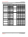
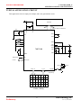
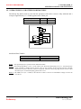
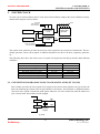
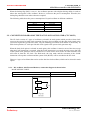
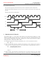
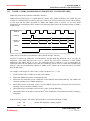
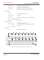
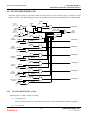
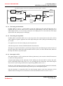
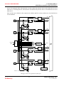
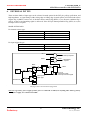
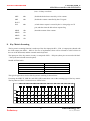
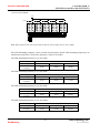
1
TM87P18M 4-Bit Microcontroller with LCD Driver User Manual tenx reserves the right to change or discontinue the manual and online documentation to this product herein to improve reliability, function or design without further notice. tenx does not assume any liability arising out of the application or use of any product or circuit described herein; neither does it convey any license under its patent rights nor the rights of others. tenx products are not designed, intended, or authorized for use in life support appliances, devices, or systems. If Buyer purchases or uses tenx products for any such unintended or unauthorized application, Buyer shall indemnify and hold tenx and its officers, employees, subsidiaries, affiliates and distributors harmless against all claims, cost, damages, and expenses, and reasonable attorney fees arising out of, directly or indirectly, any claim of personal injury or death associated with such unintended or unauthorized use even if such claim alleges that tenx was negligent regarding the design or manufacture of the part. tenx technology inc. Rev 1.0, 2012/10/05 UM-TM87P18M_E 4-Bit Microcontroller with LCD Driver Advance Information AMENDMENT HISTORY Version Date V1.0 Jul, 2012 Description New release 2 Preliminary tenx technology inc. Rev 1.0, 2012/10/05 UM-TM87P18M_E 4-Bit Microcontroller with LCD Driver Advance Information CONTENTS AMENDMENT HISTORY ................................................................................................................ 2 Chapter 1 General Description .......................................................................................................... 7 GENERAL DESCRIPTION .............................................................................................................. 7 FEATURES ......................................................................................................................................... 7 BLOCK DIAGRAM ........................................................................................................................... 9 PAD COORDINATE ........................................................................................................................ 10 PIN DESCRIPTION ......................................................................................................................... 11 CHARACTERIZATION ................................................................................................................. 12 1. 2. 3. 4. 5. 6. 7. 8. ABSOLUTE MAXIMUM RATINGS....................................................................................... 12 POWER CONSUMPTION........................................................................................................ 12 ALLOWABLE OPERATING CONDITIONS ......................................................................... 12 ALLOWABLE OPERATING FREQUENCY .......................................................................... 13 INTERNAL RC FREQUENCY RANGE ................................................................................. 13 ELECTRICAL CHARACTERISTICS...................................................................................... 13 DC Output Characteristics ......................................................................................................... 13 Segment Driver Output Characteristics ..................................................................................... 14 TYPICAL APPLICATION CIRCUIT ........................................................................................... 15 Chapter 2 TM87P18M Internal System Architecture.................................................................. 16 1. Power Supply ................................................................................................................................ 16 1-1. NO BIAS USING A Li BATTERY POWER SUPPLY ......................................................... 16 1-2. 1/2 BIAS USING A Li BATTERY POWER SUPPLY ......................................................... 17 1-3. BIAS AT Li BATTERY POWER SUPPLY .......................................................................... 18 2. SYSTEM CLOCK........................................................................................................................ 19 2-1. CONNECTION DIAGRAM OF SLOW CLOCK OSCILLATOR (XT CLOCK) ................ 19 2-2. CONNECTION DIAGRAM OF THE FAST CLOCK OSCILLATOR (CF CLOCK) ......... 20 2-2-1. RC oscillator with External Resistor, connection diagram is shown below: ................. 20 2-2-2. External 3.58 MHz Ceramic Resonator Oscillator ......................................................... 21 2-2-3. Internal RC Oscillator..................................................................................................... 21 2-3. THE COMBINATION OF THE CLOCK SOURCES ........................................................... 22 2-3-1. Dual Clock ...................................................................................................................... 22 2-3-2. Single Clock ................................................................................................................... 23 2-4. PREDIVIDER ......................................................................................................................... 25 2-5. System Clock Generator ......................................................................................................... 26 3. PROGRAM COUNTER (PC)..................................................................................................... 26 4. PROGRAM/TABLE MEMORY ................................................................................................ 27 4-1. INSTRUCTION ROM (PROM) ............................................................................................. 29 4-2. TABLE ROM (TROM) .......................................................................................................... 29 5. INDEX ADDRESS REGISTER (@HL) .................................................................................... 30 3 Preliminary tenx technology inc. Rev 1.0, 2012/10/05 UM-TM87P18M_E 4-Bit Microcontroller with LCD Driver Advance Information 6. STACK REGISTER (STACK) ................................................................................................... 31 7. DATA MEMORY (RAM) ........................................................................................................... 32 8. WORKING REGISTER (WR) ................................................................................................... 32 9. ACCUMULATOR (AC) .............................................................................................................. 33 10. ALU (Arithmetic and Logic Unit) ............................................................................................ 33 11. HEXADECIMAL CONVERT TO DECIMAL (HCD) .......................................................... 33 12. TIMER 1 (TMR1) ...................................................................................................................... 34 12-1. NORMAL OPERATION ..................................................................................................... 35 12-2. RE-LOAD OPERATION ..................................................................................................... 36 13. TIMER 2 (TMR2) ...................................................................................................................... 38 13-1. NORMAL OPERATION ..................................................................................................... 38 13-2. RE-LOAD OPERATION ..................................................................................................... 39 13-3. TIMER 2 (TMR2) IN RESISTOR TO FREQUENCY CONVERTER (RFC) .................... 40 14. STATUS REGISTER (STS) ..................................................................................................... 42 14-1. 14-2. 14-3. 14-4. 14-5. 14-6. STATUS REGISTER 1 (STS1) ........................................................................................... 42 STATUS REGISTER 2 (STS2) ........................................................................................... 43 STATUS REGISTER 3 (STS3) ........................................................................................... 44 STATUS REGISTER 3X (STS3X) ...................................................................................... 44 STATUS REGISTER 4 (STS4) ........................................................................................... 45 START CONDITION FLAG 11 (SCF11) ........................................................................... 46 15. CONTROL REGISTER (CTL)................................................................................................ 47 15-1. CONTROL REGISTER 1 (CTL1) ....................................................................................... 47 15-1-1. The Setting for Halt Mode .............................................................................................. 48 15-1-2. The Setting for Stop Mode ............................................................................................. 48 15-1-3. Interrupt for CTL1 .......................................................................................................... 48 15-2. CONTROL REGISTER 2 (CTL2) ....................................................................................... 49 15-3. CONTROL REGISTER 3 (CTL3) ....................................................................................... 49 15-4. CONTROL REGISTER 4 (CTL4) ....................................................................................... 50 16. HALT FUNCTION .................................................................................................................... 51 17. BACK UP FUNCTION ............................................................................................................. 52 18. STOP FUNCTION (STOP) ...................................................................................................... 53 Chapter 3 Control Function............................................................................................................. 55 1. ERRUPT FUNCTION ................................................................................................................. 55 1-1. RUPT REQUEST AND SERVICE ADDRESS ..................................................................... 57 1-1-1. External Interrupt Factor ................................................................................................ 57 1-1-2. Internal Interrupt Factor ................................................................................................. 57 1-2. INTERRUPT PRIORITY ....................................................................................................... 58 1-3. INTERRUPT SERVICING .................................................................................................... 59 2. RESET FUNCTION .................................................................................................................... 60 4 Preliminary tenx technology inc. Rev 1.0, 2012/10/05 UM-TM87P18M_E 4-Bit Microcontroller with LCD Driver Advance Information 2-1. POWER ON RESET............................................................................................................... 60 2-2. RESET PIN RESET ................................................................................................................ 60 2-2-1. Level Reset ..................................................................................................................... 61 2-2-2. Pulse Reset...................................................................................................................... 61 2-2-3. IOC Port/Key Matrix RESET ......................................................................................... 62 2-2-4. WATCHDOG RESET.................................................................................................... 63 3. OCK GENERATOR .................................................................................................................... 64 3-1. 3-2. 3-3. 3-4. REQUENCY GENERATOR.................................................................................................. 64 Melody APPLICATION ......................................................................................................... 65 Halver / Doubler / Tripler ....................................................................................................... 66 Alternating Frequency for LCD .............................................................................................. 66 4. BUZZER OUTPUT PINS ........................................................................................................... 66 4-1. SOUND EFFECT APPLICATION ........................................................................................ 67 4-2. REMOTE CONTROLLER APPLICATION.......................................................................... 68 5. INPUT / OUTPUT PORTS ......................................................................................................... 69 5-1. OA PORT................................................................................................................................ 69 5-1-1. Pseudo Serial Output ...................................................................................................... 70 5-2. IOB PORT .............................................................................................................................. 72 5-3. IOC PORT .............................................................................................................................. 73 5-3-1. Chattering Prevention Function and Halt Release .......................................................... 75 5-4. IOD PORT .............................................................................................................................. 76 5-4-1. Chattering Prevention Function and Halt Release.......................................................... 76 6. EXTERNAL INT PIN ................................................................................................................. 78 7. Resistor to Frequency Converter (RFC) .................................................................................... 79 7-1. 7-2. 7-3. 7-4. RC Oscillation Network .......................................................................................................... 81 Enable/Disable the Counter by Software ................................................................................ 81 Enable / Disable the Counter by Timer 2 ................................................................................ 83 Enable / Disable the Counter by CX Signal ............................................................................ 84 8. Key Matrix Scanning ................................................................................................................... 85 CHAPTER 4 LCD/LED DRIVER OUTPUT ................................................................................. 90 1. LCD LIGHTING SYSTEM IN TM87P18M ............................................................................. 90 2. DC OUTPUT ................................................................................................................................ 92 3. SEGMENT CIRCUIT FOR LCD DISPLAY ............................................................................ 93 3-1. PRINCIPLE OF OPERATION OF LCD DRIVER SECTION .............................................. 93 3-2. Relative Instructions ............................................................................................................... 96 3-1. THE CONFIGURATION of LCD RAM Area ....................................................................... 97 4. LED DRIVER OUTPUT ............................................................................................................. 98 Chapter 5 Detail Explanation of TM87P18M Instructions ........................................................ 104 1. INPUT / OUTPUT INSTRUCTIONS ...................................................................................... 104 5 Preliminary tenx technology inc. Rev 1.0, 2012/10/05 UM-TM87P18M_E 4-Bit Microcontroller with LCD Driver Advance Information 2. ACCUMULATOR MANIPULATION INSTRUCTIONS AND MEMORY MANIPULATION INSTRUCTIONS ........................................................................................... 110 3. OPERATION INSTRUCTIONS .............................................................................................. 112 4. LOAD/STORE INSTRUCTIONS ............................................................................................ 121 5. CPU CONTROL INSTRUCTIONS ......................................................................................... 123 6. INDEX ADDRESS INSTRUCTIONS ...................................................................................... 126 7. DECIMAL ARITHMETIC INSTRUCTIONS ....................................................................... 127 8. JUMP INSTRUCTIONS ........................................................................................................... 128 9. MISCELLANEOUS INSTRUCTIONS ................................................................................... 130 Appendix A TM87P18M Instruction Table ................................................................................. 135 6 Preliminary tenx technology inc. Rev 1.0, 2012/10/05 UM-TM87P18M_E 4-Bit Microcontroller with LCD Driver Advance Information Chapter 1 General Description GENERAL DESCRIPTION The TM87P18M is a One Time PROM embedded high-performance 4-bit microcontroller with LCD driver. It contains all the following functions on a single chip: 4-bit parallel processing ALU, ROM, RAM, I/O ports, timer, clock generator, dual clock operation, Resistance to Frequency Converter (RFC), LCD driver, look-up table, watchdog timer and key matrix scanning circuitry. FEATURES 1. Powerful instruction set (173 instructions). Binary addition, subtraction, BCD adjusts, logical operation in direct and index addressing mode. Single-bit manipulation (set, reset, decision for branch). Various conditional branches. 16 working registers and manipulation. Table look-up. LCD driver data transfer. 2. 3. Memory capacity. Program ROM capacity 4096 x 16 bits Data RAM capacity 512 x 4 bits. Input/output ports. Port IOA 4 pins (with internal pull-low), muxed with SEG24~SEG27. Port IOB 4 pins (with internal pull-low), muxed with SEG28~SEG30, DC31. Port IOC 4 pins (with internal pull-low, low-level-hold, chattering prevention clock). Port IOD 4 pins (with internal pull-low, chattering prevention clock). 4. 8-level subroutine nesting. 5. Interrupt function. External factor 4 (INT pin, Port IOC, IOD & KI input). Internal factor 4 (Pre-Divider, Timer1, Timer2, RFC). 6. Built-in Alarm, Frequency or Melody generator. 7. BZB, BZ (Muxed with IOB3/SE30, IOB4/DC31). 8. Built-in R to F Converter circuit. CX, RR, RT, RH (Muxed with IOA1~IOA4/ SEG24 ~ SEG27). 9. Built-in KEY_BOARD scanning function. K1~K16 (Share with SEG1~SEG16). KI1~KI4 (Muxed with IOC1~IOC4). 7 Preliminary tenx technology inc. Rev 1.0, 2012/10/05 UM-TM87P18M_E 4-Bit Microcontroller with LCD Driver Advance Information 10. Two 6-bit programmable timers with programmable clock source. 11. Watch dog timer. 12. LCD driver output. 8 common outputs and 32 segment outputs (drive up to 256 LCD segments). 1/2 ~ 1/8 Duty for LCD/LED. 1/2 Bias or 1/3 Bias for LCD/LED selected by option. Single instruction to turn off all segments. COM5~8, DC9/OD9, SEG17~ SEG23, DC31/OD31, SEG40, SEG41 can be defined as CMOS or P_open drain output type output in mask option. 32 LCD address. 13. Built-in Voltage doubler, halve charge pump circuit. 14. Dual clock operation Slow clock oscillation can be defined as X‟tal or external RC type oscillator in mask option. Fast clock oscillation can be defined as 3.58 MHz ceramic resonator, internal R in external R type oscillator by mask option. 15. HALT function. 16. STOP function. 17. ROM code protect fuse. 8 Preliminary tenx technology inc. Rev 1.0, 2012/10/05 UM-TM87P18M_E 4-Bit Microcontroller with LCD Driver Advance Information BLOCK DIAGRAM COM1-8 DC9, SEG1-30,40,41 B1-4 A1-4 C1-4 D1-4 B-PORT ALARM A-PORT RFC C-PORT KEY-IN D-PORT 31 VDD2 VDD1 VDD3 LCD DRIVER FIXED SEGMENT PLA 4 BITS DATA BUS FREQUENCY GENERATOR INDEX ROM 256(16-N) X 8 BITS PRE-DIVIDER 6 BITS PRESET TIMER1 & 2 8 LEVELS STACK CONTROL CIRCUIT 12 BITS PROGRAM COUNTER OSCILLATOR CUP1,2 XIN,OUT CFIN,OUT RESET INT ALU DATA RAM 512 X 4 BITS INSTRUCTION DECODER PROGRAM ROM (2048+128N) X 16 BITS N:0->16 TM87P18M BLOCK DIAGRAM 9 Preliminary tenx technology inc. Rev 1.0, 2012/10/05 UM-TM87P18M_E 4-Bit Microcontroller with LCD Driver Advance Information PAD COORDINATE No 1 2 3 4 5 6 7 8 9 10 11 12 13 14 15 16 17 18 19 20 21 22 23 24 25 26 27 28 29 30 31 32 Name BAK XIN XOUT CFIN CFOUT GND VDD1 VDD2 VDD3 CUP1 CUP2 COM1 COM2 COM3 COM4 COM5/DC5/OD5 COM6/DC6/OD6 COM7/DC7/OD7 COM8/DC8/OD8 DC9/OD9 SEG1 (K1) SEG2 (K2) SEG3 (K3) SEG4 (K4) SEG5 (K5) SEG6 (K6) SEG7 (K7) SEG8 (K8) SEG9 (K9) SEG10 (K10) SEG11 (K11) SEG12 (K12) No 33 34 35 36 37 38 39 40 41 42 43 44 45 46 47 48 49 50 51 52 53 54 55 56 57 58 59 60 61 62 63 64 10 Preliminary Name SEG13 (K13) SEG14 (K14) SEG15 (K15) SEG16 (K16) SEG17/DC17/OD17 SEG18/DC18/OD18 SEG19/DC19/OD19 SEG20/DC20/OD20 SEG21/DC21/OD21 SEG22/DC22/OD22 SEG23/DC23/OD23 SEG24/IOA1/CX SEG25/IOA2/RR SEG26/IOA3/RT SEG27/IOA4/RH SEG28/IOB1 SEG29/IOB2 SEG30/IOB3/BZB DC31/OD31/IOB4/BZ IOC1/KI1 IOC2/KI2 IOC3/KI3 IOC4/KI4 IOD1 IOD2 IOD3 IOD4 SEG40/DC40/OD40 SEG41/DC41/OD41 RESET INT VPP tenx technology inc. Rev 1.0, 2012/10/05 UM-TM87P18M_E 4-Bit Microcontroller with LCD Driver Advance Information PIN DESCRIPTION Name I/O BAK P VDD2 P VDD1, 3 P RESET I INT I I/O CUP1, 2 O XIN XOUT I O CFIN CFOUT I O COM1~8 O DC9,31 SEG1-30,40, 41 O O IOA1-4 I/O IOB1-4 I/O IOC1-4 I/O IOD1-4 I/O (RFC)CX RR/RT/RH (ALM) BZB/BZ I O KI1~4 I GND P VPP P O Description Positive Back-up voltage, connect a 0.1u capacitor to GND. Positive voltage is needed to BAK pin for Serial Program/Read Mode. Positive supply voltage. Connect +3.0V battery positive pin to VDD2. Positive voltage is needed to VDD2 for Serial Program/Read Mode. LCD supply voltage, and positive supply voltage. Positive voltage is needed to VDD3 for Serial Program/Read Mode. Input pin from LSI reset request signal, with internal pull-down resistor. Instruction Reset Time can select “PH15/2” or “PH12/2” by option. Reset Type can select “Level” or “Pulse” by option. Signal for Serial Program/Read Mode. Input pin for external INT request signal. Falling edge or rising edge triggered by option. Internal pull-down or pull-up resistor is selected by option. Signal for Serial Program/Read Mode. Switching pins for supply the LCD driving voltage to the VDD1, VDD2, VDD3 pins. Connect the CUP1 and CUP2 pins with non-polarized electrolytic capacitor if 1/2 or 1/3 bias mode has been selected. In no BIAS mode, these pins should be open. Low speed oscillator, generates clock for time base functions (clock specified, LCD alternating frequency, Alarm signal frequency) or system clock oscillation. 32KHz Crystal oscillator for Slow Clock. High speed oscillator, system clock oscillation for FAST clock only or DUAL clock operation. The usage of 3.58 MHz ceramic/resonator oscillator or external R type oscillator is defined by mask option. Output pins for driving the common pins of the LCD or LED panel. COM5~8 is muxed with DC/Open Drain, and set mask option. DC/Open Drain Output pins for driving the LCD or LED panel segment. Input / Output port A, can use software to define internal pull-low Resistor. This port is muxed with SEG24~27, and set by option. Input / Output port B, can use software to define internal pull-low Resistor. This port is muxed with SEG28~30, DC31 / BZB, BZ, and set by option. Input / Output port C, can use software to define internal pull-low / low-level-hold Resistor and Chattering clock to reduce input bounce. This port is muxed with KI1~4, and set by option. Input / Output port D, can use software to define internal pull-low Resistor, and Chattering clock to reduce input bounce. 1 input pin and 3 output pins for RFC application. This port is muxed with SEG24~27 / IOA1~4, and set by option. Output port for alarm, frequency or melody generator This port is muxed with SEG 30, DC 31 / IOB3, 4, and set by option. Keyboard scanning input port. This port is muxed with IOC1~4, and set by option. Negative supply voltage. Connect for Serial Program/Read Mode. High Voltage is need to VPP for Serial Program/Read Mode. Connected VDD2 to VPP or floating for Normal Mode. Serial Program/Read Connect Pins: VPP, VDD2, VDD3, GND, RESET, INT, BAK 11 Preliminary tenx technology inc. Rev 1.0, 2012/10/05 UM-TM87P18M_E 4-Bit Microcontroller with LCD Driver Advance Information CHARACTERIZATION 1. ABSOLUTE MAXIMUM RATINGS (GND= 0V) Name Maximum Supply Voltage Maximum Input Voltage Maximum Output Voltage Maximum Operating Temperature Maximum Storage Temperature Symbol VDD1 VDD2 VDD3 VPP Vin Vout1 Vout2 Topg Tstg Range -0.3 to 5.5 -0.3 to 5.5 -0.3 to 8.5 -0.3 to 13.5 -0.3 to VDD1/VDD2+0.3 -0.3 to VDD1/VDD2+0.3 -0.3 to VDD3+0.3 -40 to +80 -25 to +125 Unit V V V V V V V ℃ ℃ 2. POWER CONSUMPTION (At VDD2=3.0V, Ta=-40℃ to 80℃, GND= 0V) Name HALT mode STOP mode Normal Mode External R 3.58 MHz ceramic resonator Sym. Condition Only 32.768 KHz Crystal oscillator operating, IHALT without loading. BCF = 0, 1/4 duty, ph0=BCLK ISTOP Only 32.768 KHz Crystal oscillator operating, I32K without loading. BCF = 0, 1/4 duty, ph0=BCLK R = 150 KΩ oscillator operating, without loading. IExt. R BCF = 0, 1/4 duty, ph0=BCLK Only 3.58 MHz ceramic resonator operating, without I3.58Mcr loading. BCF = 0, 1/4 duty, ph0=BCLK Min. Typ. Max. Unit 3 6 uA 1 uA 8 uA 36 uA 480 uA Note: When External R oscillator mode is operating, the current consumption will depend on the frequency of oscillation. 3. ALLOWABLE OPERATING CONDITIONS (At Ta=-40℃ to 80℃, GND= 0V) Name Supply Voltage Oscillator Start-Up Voltage Oscillator Sustain Voltage Supply Voltage Input “H” Voltage Input “L” Voltage Input “H” Voltage Input “L” Voltage Input “H” Voltage Input “L” Voltage Operating Freq Symb. VDD2 VDD3 VPP VDDstup VDDsut VDD2 Vih1 Vil1 Vih2 Vil2 Vih3 Vil3 Fopg1 Fopg2 Condition 32.768 KHz Crystal Mode 3.58 ceramic resonator Mode 32.768 KHz Crystal Mode 3.58 ceramic resonator Mode Li Mode Li Battery Mode OSCIN at Li Battery Mode CFIN at Li Battery 32.768 KHz Crystal Mode External R mode 12 Preliminary Min. 2.4 2.4 2.4 1.4 1.8 1.3 1.55 2.4 VDD2-0.7 -0.7 0.8xVDD2 0 0.8xVDD2 0 32 10 Max. 5.25 8.0 12.5 3.6 VDD2+0.7 0.7 VDD2 0.2xVDD2 VDD2 0.2xVDD2 1000 Unit V V V V V V V V V V V V V V KHz KHz tenx technology inc. Rev 1.0, 2012/10/05 UM-TM87P18M_E 4-Bit Microcontroller with LCD Driver Advance Information 4. ALLOWABLE OPERATING FREQUENCY (At Ta=-40℃ to 80℃, GND= 0V) Condition BAK=3V Max. Operating Frequency 4 MHz 5. INTERNAL RC FREQUENCY RANGE Option Mode BAK Min. Typ. Max. 250 KHz 3.0V 200 KHz 250 KHz 300 KHz 500 KHz 3.0V 400 KHz 500 KHz 600 KHz 6. ELECTRICAL CHARACTERISTICS At#1:VDD2=3.0V(Li); At#2:VDD2=5.0V; Input Resistance Name “L” Level Hold Tr(IOC) IOA,B,C Pull-Down Tr INT Pull-up Tr INT Pull-Down Tr RES Pull-Down R Symb. Rllh1 Rllh2 Rmad1 Rmad2 Rintu1 Rintu2 Rintd1 Rintd2 Rres Condition Vi=0.2VDD2,#1 Vi=0.2VDD2,#2 Vi=VDD2,#1 Vi=VDD2,#2 Vi=VDD2,#1 Vi=VDD2,#2 Vi=GND,#1 Vi=GND,#2 Vi=GND or VDD2,#1,#2 Min. 10 5 200 100 200 100 200 100 10 Typ. 40 20 500 250 500 250 500 250 45 Max. 100 50 1000 500 1000 500 1000 500 100 Unit KΩ KΩ KΩ KΩ KΩ KΩ KΩ KΩ KΩ Min. 2.0 3.2 Typ. Max. Unit V V V V V V V V 7. DC Output Characteristics At#3:VDD2=2.4V(Li); At#4:VDD2=4.0V; Name Output “H” Voltage Output “L” Voltage Output “H” Voltage Output “L” Voltage Symb. Voh3c Voh4c Vol3c Vol4c Voh3c Voh4c Vol3c Vol4c Condition Ioh=-1 mA,#3 Ioh=-3 mA,#4 Iol=2 mA,#3 Iol=6 mA,#4 Ioh=-3 mA,#3 Ioh=-5 mA,#4 Iol=5 mA,#3 Iol=10 mA,#4 13 Preliminary Port COM5~8,DC9 SEG28~30,DC31, SEG40,41, IOC, IOD SEG24~27,INT 0.4 0.8 2.0 3.2 0.4 0.8 tenx technology inc. Rev 1.0, 2012/10/05 UM-TM87P18M_E 4-Bit Microcontroller with LCD Driver Advance Information 8. Segment Driver Output Characteristics Name Output “H” Voltage Output “L” Voltage Output “H” Voltage Symb. Voh3f Voh4f Vol3f Vol4f Voh3g Voh4g Vom3g Output “M” Voltage Vom4g Output “L” Voltage Vol3g Vol4g Output “H” Voltage Voh3i Voh4i Vom13i Output “M1” Voltage Vom14i Vom23i Output “M2” Voltage Vom24i Output “L” Voltage Output “H” Voltage Vol3i Vol4i Voh3j Voh4j Vom13j Output “M1” Voltage Vom14j Vom23j Output “M2” Voltage Vom24j Output “L” Voltage Vol3j Vol4j Condition For 1/2 Bias Display Mode Ioh=-1 uA,#3 Ioh=-1 uA,#4 SEG-n Iol=1 uA,#3 Iol=1 uA,#4 Ioh=-10 uA,#3 COM-n Ioh=-10 uA,#4 Iol/h=+/-10 uA,#3 Iol/h=+/-10 COM-n uA,#4 Iol=10 uA,#3 Iol=10 uA,#4 1/3 Bias display Mode Ioh=-1 uA,#3 Ioh=-1 uA,#4 Iol/h=+/-10 uA,#3 Iol/h=+/-10 uA,#4 SEG-n Iol/h=+/-10 uA,#3 Iol/h=+/-10 uA,#4 Iol=1 uA,#3 Iol=1 uA,#4 Ioh=-10 uA,#3 Ioh=-10 uA,#4 Iol/h=+/-10 uA,#3 Iol/h=+/-10 uA,#4 COM-n Iol/h=+/-10 uA,#3 Iol/h=+/-10 uA,#4 Iol=10 uA,#3 Iol=10 uA,#4 14 Preliminary Min. Typ. Max. Unit. 0.2 0.2 V V V V V V 1.0 1.4 V 1.8 2.2 V 0.2 0.2 V V 2.2 3.8 2.2 3.8 3.4 5.8 V V 1.0 1.4 V 1.8 2.2 V 2.2 2.6 V 3.8 4.2 V 0.2 0.2 V V V V 1.0 1.4 V 1.8 2.2 V 2.2 2.6 V 3.8 4.2 V 0.2 0.2 V V 3.4 5.8 tenx technology inc. Rev 1.0, 2012/10/05 UM-TM87P18M_E 4-Bit Microcontroller with LCD Driver Advance Information TYPICAL APPLICATION CIRCUIT This application circuit is simply an example, and is not guaranteed to work. LCD Panel 3.58MHz Ceramic 15P CFIN CFOUT 15P XIN 32.768KHz Crystal COM1~8, SEG1~23, SEG40,41 CUP1 XOUT 0.1u CUP2 RH RT VDD3 RR VPP VDD(2) CX 0.1u VDD1 TM87P18M 0.1u I/O Port BAK 0.1u 3.0V 0.1u GND RESET External INT. 0.1u INT IOB,IOC,IOD Choke SEG1~16 K1~K4 Buzzer BZ(BZB) Key Scaning Key Matrix 1/3 Bias, 1/8Duty 15 Preliminary tenx technology inc. Rev 1.0, 2012/10/05 0.1u UM-TM87P18M_E 4-Bit Microcontroller with LCD Driver Advance Information Chapter 2 TM87P18M Internal System Architecture 1. Power Supply TM87P18M can operate at Li, all of these operating types are defined by mask option. The power supply circuitry is also generated by the necessary voltage level to drive the LCD panel with different bias. Shown below are the connection diagrams for 1/2 bias, 1/3 bias application. LI BATTERY POWER SUPPLY Operating voltage range: 2.4V ~ 5.25V. For different LCD bias application, the connection diagrams are shown below: 1-1. NO BIAS USING A Li BATTERY POWER SUPPLY N.C. N.C. CUP1 CUP2 GND BAK VDD1 VDD2 VDD3 + Application circuit TM87P18M MASK OPTION TABLE: Mask Option name POWER SOURCE BIAS Selected item (2) 3V BATTERY OR HIGHER (1) NO BIAS Note 1: The input/output ports operate between GND and VDD2. 16 Preliminary tenx technology inc. Rev 1.0, 2012/10/05 UM-TM87P18M_E 4-Bit Microcontroller with LCD Driver Advance Information 1-2. 1/2 BIAS USING A Li BATTERY POWER SUPPLY The backup flag (BCF) must be reset after the operation of the halver circuit is fully stabilized and a voltage of approximately 1/2 * VDD2 appears on the VDD1 pin. Backup flag(BCF) BCF=0 BCF=1 SW1 ON OFF SW2 OFF ON CUP1 0.1u CUP2 VDD3 VDD2 SW2 VDD1 SW1 BAK Internal logic 0.1u 3.0V 0.1u GND MASK OPTION TABLE: Mask Option name POWER SOURCE BIAS Selected item (2) 3V BATTERY OR HIGHER (2) 1/2 BIAS Note 1: The input/output ports operate between GND and VDD2. Note 2: The backup flag (BCF) is set to 1 in the initial cycle. When the backup flag is set to 1, the internal logic signal operated on VDD2 and the driving power of the oscillator circuit increases and the operating current also increases. Therefore, unless it is required, otherwise, the backup flag must be reset to 0 after the initial cycle. For the backup flag, please refer to 2-17. Note 3: The VDD1 level (1/2 * VDD2) in the off-state of SW1 is used as an intermediate voltage level for the LCD driver. 17 Preliminary tenx technology inc. Rev 1.0, 2012/10/05 UM-TM87P18M_E 4-Bit Microcontroller with LCD Driver Advance Information 1-3. BIAS AT Li BATTERY POWER SUPPLY The backup flag (BCF) must be reset after the operation of the halver circuit is fully stabilized and a voltage of approximately 1/2 * VDD2 appears on the VDD1 pin. Backup flag (BCF) BCF=0 BCF=1 SW1 ON OFF SW2 OFF ON CUP1 0.1u CUP2 VDD3 SW2 VDD2 SW1 VDD1 Internal logic BAK 0.1u 0.1u 3.0V 0.1u GND MASK OPTION TABLE: Mask Option name POWER SOURCE BIAS Selected item (2) 3V BATTERY OR HIGHER (3) 1/3 BIAS Note 1: The input/output ports operate between GND and VDD2. Note 2: The backup flag (BCF) is set to 1 in the initial cycle. When the backup flag is set to 1, the internal logic signal is operated on VDD2 and the driving power of the oscillator circuit increases and the operating current also increases. Therefore, unless it is required, otherwise, the backup flag must be reset to 0 after the initial cycle. For the backup flag, please refer to 2-17. Note 3: The VDD1 level (1/2 * VDD) in the off-state of SW1 is used as an intermediate voltage level for LCD driver. 18 Preliminary tenx technology inc. Rev 1.0, 2012/10/05 UM-TM87P18M_E 4-Bit Microcontroller with LCD Driver Advance Information 2. SYSTEM CLOCK XT clock (slow clock oscillator) and CF clock (fast clock oscillator) compose the clock oscillation circuitry and the block diagram is shown below. Stop, Halt Fast instruction Slow instruction BCLK T1 T2 T3 T4 Sclk XT Clock Clock switch circuit CF Clock Clock switch circuit System clock generator PH Predivider Single clock option Dual clock option The system clock generator provides the necessary clock signals for the execution of instructions. The predivider generates various clock signals of different frequencies for the LCD driver, frequency generator, etc… The following table shows the clock sources of system clock generator and the pre-divider under different conditions. PH0 XT clock CF clock XT clock XT clock XT clock XT clock Slow clock only option fast clock only option Initial state (dual clock option) Halt mode (dual clock option) Slow mode (dual clock option) Fast mode (dual clock option) BCLK XT clock CF clock XT clock XT clock XT clock CF clock 2-1. CONNECTION DIAGRAM OF SLOW CLOCK OSCILLATOR (XT CLOCK) This oscillator provides the lower-speed clock signals to the system clock generator, the pre-divider, the timer, the chattering prevention of the IO port and the LCD circuitry. This oscillator is disabled when the “fast clock only” option is selected in mask option; otherwise it is active all the time after the initial reset cycle. In stop mode, the oscillator will be stopped. 15pf XOUT 15pf XIN 32768Hz Crystal (1) X'tal 19 Preliminary tenx technology inc. Rev 1.0, 2012/10/05 UM-TM87P18M_E 4-Bit Microcontroller with LCD Driver Advance Information When the backup flag (BCF) is set to 1, the oscillator operates with a higher driving ability in order to reduce the start-up time of the oscillator. However, it increases the power consumption. Therefore, the backup flag should be reset unless otherwise required. The following table shows the power consumption of Crystal oscillator in different conditions: Li power option Increased Normal Increased Normal BCF=1 BCF=0 Initial reset After reset 2-2. CONNECTION DIAGRAM OF THE FAST CLOCK OSCILLATOR (CF CLOCK) The CF clock consists of 3 types of oscillators (selectable in mask option) which provide a faster clock source to the system. In single clock operation (fast only), this oscillator provides the clock signals to the system clock generator, pre-divider, timer, I/O port chattering prevention clock and the LCD circuitry. In dual clock operation, CF clock provides the clock signals to the system clock generator only. When the dual clock option is selected in mask option, this oscillator is inactive most of the time except when the FAST instruction is executed. After the FAST instruction is executed, the clock source (BCLK) of the system clock generator will be switched to CF clock, but the clock source for other functions will still come in from the XT clock. The Halt mode, the stop mode and the execution of the SLOW instruction will stop this oscillator and the system clock (BCLK) will be switched to the XT clock. There are 3 types of oscillators that can be used as the fast clock oscillator, which can be selected in mask option: 2-2-1. RC oscillator with External Resistor, connection diagram is shown below: MASK OPTION TABLE: Mask Option name FAST CLOCK TYPE FOR FAST ONLY OR DUAL Selected item (3) EXTERNAL RESISTOR CFOUT R CFIN External Resistor 20 Preliminary tenx technology inc. Rev 1.0, 2012/10/05 UM-TM87P18M_E 4-Bit Microcontroller with LCD Driver Advance Information 2-2-2. External 3.58 MHz Ceramic Resonator Oscillator MASK OPTION TABLE: Mask Option name FAST CLOCK TYPE FOR FAST ONLY OR DUAL Selected item (4) 3.58 MHz Ceramic Resonator CFOUT CFIN 3.58MHz Ceramic Resonator Notes: 1. If it is required to reset the BCF to 0 in Li battery power mode, do not use a 3.58 MHz Ceramic Resonator as the oscillator. 2-2-3. Internal RC Oscillator MASK OPTION TABLE: For 250 KHz output frequency: Mask Option name FAST CLOCK TYPE FOR FAST ONLY OR DUAL Selected item (1) INTERNAL RESISTOR FOR 250 KHz For 250 KHz output frequency: Mask Option name FAST CLOCK TYPE FOR FAST ONLY OR DUAL Selected item (2) INTERNAL RESISTOR FOR 500 KHz CFOUT N.C. CFIN N.C. Internal RC FREQUENCY RANGE OF INTERNAL RC OSCILLATOR Option Mode 250 KHz 500 KHz BAK 3.0V 3.0V Min. 200 KHz 400 KHz 21 Preliminary Typ. 250 KHz 500 KHz Max. 300 KHz 600 KHz tenx technology inc. Rev 1.0, 2012/10/05 UM-TM87P18M_E 4-Bit Microcontroller with LCD Driver Advance Information 2-3. THE COMBINATION OF THE CLOCK SOURCES There are three types of combination of the clock sources that can be selected by mask option: 2-3-1. Dual Clock MASK OPTION TABLE: Mask Option name CLOCK SOURCE Selected Item (3) DUAL The operation of the dual clock mode is shown in the following figure. When this mode is selected in mask option, the clock source (BCLK) of the system clock generator will switch between the XT clock and the CF clock according to the user‟s program. When the HALT and STOP instructions are executed, the clock source (BCLK) will switch to the XT clock automatically. The XT clock provides the clock signals to the pre-divider, the timer, the I/O port chattering prevention and the LCD circuitry in this mode. Halt Halt mode XTOSC:active CFOSC:stop Halt HALT released Stop released Power-on reset Reset pin reset Watchdog timer reset Key reset Slow mode XTOSC:active CFOSC:stop Reset release Slow Fast Fast mode XTOSC: active CFOSC: active Stop Reset Reset state XTOSC:active CFOSC:stop Reset Stop mode XTOSC: stop CFOSC: stop The state diagram of the dual clock mode is shown the above figure. After the execution of the FAST instructions, the system clock generator will hold for 12 CF clock cycles after the CF clock oscillator starts up and then BCLK will switch to the CF clock. It prevents the delivery of incorrect clock signals to the system clock in the start-up duration of the fast clock oscillator. 22 Preliminary tenx technology inc. Rev 1.0, 2012/10/05 UM-TM87P18M_E 4-Bit Microcontroller with LCD Driver Advance Information C F clo ck X T clo ck F A S T B C L K H O L D1 2C FC L O C K S This figure shows the System Clock Switching from Slow to Fast After executing SLOW instruction, the system clock generator will hold for 2 XT clock cycles, and then BCLK will switch to the XT clock. C F clo ck F a st clo cksto p so p e ra tin g X T clo ck S L O W B C L K This figure shows the System Clock Switching from Fast to Slow 2-3-2. Single Clock MASK OPTION TABLE: For Fast clock oscillator only Mask Option name CLOCK SOURCE (1) Selected item FAST ONLY For slow clock oscillator only Mask Option name CLOCK SOURCE Selected item (2) SLOW ONLY The operation of the single clock option is shown in the following figure. Either XT or CF clock may be selected by mask option in this mode. The FAST and SLOW instructions will perform as the NOP instruction in this option. 23 Preliminary tenx technology inc. Rev 1.0, 2012/10/05 UM-TM87P18M_E 4-Bit Microcontroller with LCD Driver Advance Information The backup flag (BCF) will be set to 1 automatically before the program enters the stop mode. This can ensure the Crystal oscillator will start up in a better condition. Normal mode OSC:active Reset release Power -on reset Reset pin reset Watchdog timer reset Key reset Halt Halt released Halt mode OSC:active Stop Reset Stop Release Reset mode OSC:active Reset Stop mode OSC: stop This figure shows the State Diagram of Single Clock Option 24 Preliminary tenx technology inc. Rev 1.0, 2012/10/05 UM-TM87P18M_E 4-Bit Microcontroller with LCD Driver Advance Information 2-4. PREDIVIDER The pre-divider is a 15-stage counter that receives the clock signals from the output of the clock switch circuitry (PH0) as input. When PH0 changes from "H" level to "L" level, the content of this counter changes accordingly. The PH11 to PH15 of the pre-divider are reset to "0" when the PLC 100H instruction is executed or in the initial reset cycle. The pre-divider delivers the signals to the halver/tripler circuit, LCD driver, sound generator and the I/O port chattering prevention function. Frequency Generator HEF3 BCLK Halt mode FAST instruction FAST instruction T1 T2 T3 T4 Sclk Clock switch circuit XTOSC Interrupt request IEF3 Initial PLC 8H Interrupt SCF7 R Q Fall edge detector System clock generator S HRF3 HALT release request flag MSC instruction Data bus 2 Clock switch circuit CFOSC To timer circuit PH0 PLC 100H initial PH7 PH15 PH14 PH13 PH8 PH12 PH6 PH11 PH5 PH4 PH3 PH2 PH1 Single clock option Dual clock option PH10 R R R R R PH9 To sound circuit Halver tribler circuit This figure shows the Pre-divider and its Peripherals The falling edge of PH14 will set the halt mode release request signal flag (HRF3), in this case, if the pre-divider interrupt enable mode (IEF3) is set in advance, the interrupt coming from predivider is accepted; and if the halt release enable mode (HEF3) is set in advance, then the halt release request signal will be delivered and the start condition flag 7 (SCF7) in status register 3 (STS3) will be set. The clock source of the pre-divider is PH0; there are 4 kinds of frequencies of PH0 that can be selected in mask option: MASK OPTION TABLE: Mask Option name PH0 <-> BCLK FOR FAST ONLY PH0 <-> BCLK FOR FAST ONLY PH0 <-> BCLK FOR FAST ONLY PH0 <-> BCLK FOR FAST ONLY 25 Preliminary Selected item (1) PH0 = BCLK (2) PH0 = BCLK/4 (3) PH0 = BCLK/8 (4) PH0 = BCLK/16 tenx technology inc. Rev 1.0, 2012/10/05 UM-TM87P18M_E 4-Bit Microcontroller with LCD Driver Advance Information 2-5. System Clock Generator The system clock generator provides the necessary clocks to control the execution of instructions. The FAST and SLOW instructions can also be used to switch the clock input of the system clock generator. The basic system clock is as shown below: SCLK T1 T2 T3 T4 Machine Cycle Instruction Cycle 3. PROGRAM COUNTER (PC) The program counter is a 12-bit counter, which addresses the program memory (ROM) up to 4096 addresses. The MSB of program counter (PC11) is a page register. Only CALL and JMP instructions can be used to address the whole address range (000h ~ FFFh), the rest of relative jump instructions can address either page 0 (000h ~ 7ffh) or page 1 (800h ~ FFFh). The program counter (PC) is normally incremented by one (+1) for every instruction execution. When executing JMP instructions, subroutine call instructions (CALL), interrupt service routine or when reset occurs, the program counter (PC) will be loaded with the corresponding address in table 2-1. Table 2- 1 When executing a jump instruction except JMP and CALL, the program counter (PC) will be loaded with the specified address in the operand of the instruction. All these relative jump instructions can only 26 Preliminary tenx technology inc. Rev 1.0, 2012/10/05 UM-TM87P18M_E 4-Bit Microcontroller with LCD Driver Advance Information be used to address the current page, that is when the current page is page 0 (PC11=0), only the range from 000h ~ 7FFh is accessible; when the current page is page 1 (PC11=1), only the range from 800h ~ FFFh is accessible. Return instruction (RTS) –1 Table 2- 1 Initial reset Interrupt 2 (INT pin) Interrupt 0 (input port C or D) Interrupt 1 (timer 1 interrupt) Interrupt 3 (pre-divider interrupt) Interrupt 4 (timer 2 interrupt) Interrupt 5 (Key Scanning interrupt) Interrupt 6 (RFC counter interrupt) Jump instruction Subroutine call PC11 PC10 0 0 PC9 0 PC8 0 PC7 0 PC6 0 PC5 0 PC4 0 PC3 0 PC2 0 PC1 0 PC0 0 0 0 0 0 0 0 0 1 0 0 0 0 0 0 0 0 0 0 0 1 0 1 0 0 0 0 0 0 0 0 0 1 1 0 0 0 0 0 0 0 0 0 0 1 1 1 0 0 0 0 0 0 0 0 1 0 0 0 0 0 0 0 0 0 0 0 1 0 0 1 0 0 0 0 0 0 0 0 1 0 1 0 0 0 P11 P11 P10 P10 P9 P9 P8 P8 P7 P7 P6 P6 P5 P5 P4 P4 P3 P3 P2 P2 P1 P1 P0 P0 P10 to P0: the 11 Low-order bits of instruction operand P11: page register When executing a subroutine call instructions or interrupt service routine, the content of the program counter (PC) are automatically saved to the stack register (STACK). 4. PROGRAM/TABLE MEMORY The built-in mask ROM is organized into 4096 x 16 bits. There are 2 pages of memory space in this mask ROM. Page 0 covers the address ranging from 000h to 7FFh and page 1 covers 800h to FFFh. 27 Preliminary tenx technology inc. Rev 1.0, 2012/10/05 UM-TM87P18M_E 4-Bit Microcontroller with LCD Driver Advance Information Page 0 000h Page 1 800h 7FFh FFFh Both instruction ROM (PROM) and table ROM (TROM) share this memory space together. The partition formula for PROM and TROM is as shown below: Instruction ROM memory space = 2048 + (128 * N) words, Table ROM memory space = 256(16 - N) bytes (N = 0 ~ 16). Note: The data width of the table ROM is 8-bit The partition of memory space is defined by mask option, the table is shown below: MASK OPTION table: Mask Option name Selected item INSTRUCTION ROM <-> TABLE ROM INSTRUCTION ROM <-> TABLE ROM INSTRUCTION ROM <-> TABLE ROM INSTRUCTION ROM <-> TABLE ROM INSTRUCTION ROM <-> TABLE ROM INSTRUCTION ROM <-> TABLE ROM INSTRUCTION ROM <-> TABLE ROM INSTRUCTION ROM <-> TABLE ROM INSTRUCTION ROM <-> TABLE ROM INSTRUCTION ROM <-> TABLE ROM INSTRUCTION ROM <-> TABLE ROM INSTRUCTION ROM <-> TABLE ROM INSTRUCTION ROM <-> TABLE ROM INSTRUCTION ROM <-> TABLE ROM INSTRUCTION ROM <-> TABLE ROM INSTRUCTION ROM <-> TABLE ROM INSTRUCTION ROM <-> TABLE ROM 1 (N=0) 2 (N=1) 3 (N=2) 4 (N=3) 5 (N=4) 6 (N=5) 7 (N=6) 8 (N=7) 9 (N=8) A (N=9) B (N=10) C (N=11) D (N=12) E (N=13) F (N=14) G (N=15) H (N=16) 28 Preliminary Instruction ROM memory space (Words) 2048 2176 2304 2432 2560 2688 2816 2944 3072 3200 3328 3456 3584 3712 3840 3968 4096 Table ROM memory space (Bytes) 4096 3840 3584 3328 3072 2816 2560 2304 2048 1792 1536 1280 1024 768 512 256 0 tenx technology inc. Rev 1.0, 2012/10/05 UM-TM87P18M_E 4-Bit Microcontroller with LCD Driver Advance Information 4-1. INSTRUCTION ROM (PROM) There are some special locations that serve as interrupt service routines, such as reset address (000H), interrupt 0 address (014H), interrupt 1 address (018H), interrupt 2 address (010H), interrupt 3 address (01CH), interrupt 4 address (020H), interrupt 5 address (024H), and interrupt 6 address (028H), in the program memory. When the valid address range of PROM exceeds 2048 addresses (800h), the memory space of PROM will automatically be defined as 2 pages. Refer to section 2-3. This figure shows the Organization of ROM 000h Initial reset 010h Interrupt 2 014h Interrupt 0 018h Interrupt 1 01Ch Interrupt 3 020h Interrupt 4 024h Interrupt 5 028h Interrupt 6 address 000H 256(16-N) addresses Address High Nibble Low Nibble XFFH 8 Bits 2048+(128*N) (N=0 ~ 16) X=15-N(N:1 -> 15) 16 bits Instruction ROM ( PROM ) organization Table ROM ( TROM ) organization 4-2. TABLE ROM (TROM) The table ROM is organized into 256(16-N) x 8 bits that shares the memory space with the instruction ROM (as shown in the figure above). This memory space stores the constant data or look up tables for the usage of the main program. All the table ROM addresses can be specified by the index address register (@HL). The data width can be 8 bits (256(16-N) x 8 bits) or 4 bits (512(16-N) x 4 bits) depending on the usage. Please refer to the explanation in the instruction chapter for details. 29 Preliminary tenx technology inc. Rev 1.0, 2012/10/05 UM-TM87P18M_E 4-Bit Microcontroller with LCD Driver Advance Information 5. INDEX ADDRESS REGISTER (@HL) This is a versatile address pointer for the data memory (RAM) and table ROM (TROM). The index address register (@HL) is a 12-bit register, and the content of the register can be modified by executing MVH, MVL and MVU instructions. The execution of the MVL instructions will load the content of the specified data memory to the lower nibble of the index register (@L). In the same manner, the execution of the MVH and MVU instructions will load the content of the data RAM (Rx) to the higher nibble of the register @H and @U, respectively. @U register Bit7 Bit6 Bit5 IDBF11 IDBF10 IDBF9 Bit4 IDBF8 Bit3 IDBF7 @H register Bit2 Bit1 IDBF6 IDBF5 Bit0 IDBF4 Bit3 IDBF3 @L register Bit2 Bit1 IDBF2 IDBF1 Bit0 IDBF0 The index address register can specify the full range addresses of the table ROM and data memory. bit3 MVU IDBF11 Rx bit0 IDBF8 bit3 IDBF7 DATA RAM MVH @H Rx IDBF4 IDBF3 bit0 bit3 index @U addressing @L MVL Rx IDBF0 bit0 @HL TABLE ROM index addressing This figure shows the diagram of the index address register The index address register is a write-only register, CPHL X instruction can specify 8-bit immediate data to compare with the content of @H and @L. If the result of the comparison is equivalent, the instruction behind CPHL X will be skipped (NOP); if it is not equivalent, the instruction behind CPHL X will be executed normally. Note: During the process of the comparison of the index address, all the interrupt enable flags (IEF) must be cleared to avoid malfunction. The comparison bit pattern is shown below: CPHL X @HL X7 IDBF7 Example: ……………… CPHL 30h SIE* 0h X6 IDBF6 X5 IDBF5 X4 IDBF4 X2 IDBF2 X1 IDBF1 X0 IDBF0 ; @HL = 30h ; disable IEF 30 Preliminary X3 IDBF3 tenx technology inc. Rev 1.0, 2012/10/05 UM-TM87P18M_E 4-Bit Microcontroller with LCD Driver Advance Information JMP lable1 JMP lable2 ……………. lable1: ……….. lable2: ; this instruction will not be executed (NOP) ; this instruction will be executed and than jump to lable2 6. STACK REGISTER (STACK) Stack is a special design register following the first-in-last-out rule. It is used to save the contents of the program counter sequentially during subroutine call or execution of the interrupt service routine. The contents of stack register are returned sequentially to the program counter (PC) while executing return instructions (RTS). The stack register is organized using 11 bits by 8 levels but with no overflow flag; hence only 8 levels of subroutine call or interrupt are allowed (If the stacks are full, and either interrupt occurs or subroutine call executes, the first level will be overwritten). Once the subroutine call or interrupt causes the stack register (STACK) overflow, the stack pointer will return to 0 and the content of the level 0 stack will be overwritten by the PC value. The contents of the stack register (STACK) are returned sequentially to the program counter (PC) during execution of the RTS instruction. Once the RTS instruction causes the stack register (STACK) underflow, the stack pointer will return to level 7 and the content of the level 7 stack will be restored to the program counter. The following figure shows the diagram of the stack. Stack pointer CALL instruction Interrupt accepted RTS instruction level 1 level 0 level 2 level 7 STACK ring with first-in, last-out function level 6 level 3 level 4 level 5 31 Preliminary tenx technology inc. Rev 1.0, 2012/10/05 UM-TM87P18M_E 4-Bit Microcontroller with LCD Driver Advance Information 7. DATA MEMORY (RAM) The static RAM is organized with 512 addresses x 4 bits and is used to store data. The data memory may be accessed using two methods: (1) Direct addressing mode The address of the data memory is specified by the instruction and the addressing range is from 00H to 7FH. (2) Index addressing mode The index address register (@HL) specifies the address of the data memory and all address space from 00H to 1FFH can be accessed. The 16 specified addresses (70H to 7FH) in the direct addressing memory are also used as 16 working registers. The function of working register will be described in detail in section 2-8. DATA RAM 70H Working Register 7FH 80H Index Address Access Direct Address Access 00H 1FFH 4 Bits This figure shows the Data Memory (RAM) and Working Register Organization 8. WORKING REGISTER (WR) The locations 70H to 7FH of the data memory (RAM) are not only used as general-purpose data memory but also as the working register (WR). The following will introduce the general usage of working registers: (1) To perform the arithmetic and logic operations on the contents of a working register and immediate data. Such as: ADCI, ADCI*, SBCI, SBCI*, ADDI, ADDI*, SUBI, SUBI*, ADNI, ADNI*, ANDI, ANDI*, EORI, EORI*, ORI, ORI* (2) To transfer data between a working register and any address in the direct addressing data memory (RAM). Such as: MWR Rx, Ry; MRW Ry, Rx (3) To decode (or directly transfer) the contents of a working register and then output to the LCD PLA circuit. Such as: 32 Preliminary tenx technology inc. Rev 1.0, 2012/10/05 UM-TM87P18M_E 4-Bit Microcontroller with LCD Driver Advance Information (4) LCT, LCB, LCP 9. ACCUMULATOR (AC) The accumulator (AC) is a register that plays the most important role in operations and controls. By using it in conjunction with the ALU (Arithmetic and Logic Unit), data transfer between the accumulator and other registers or data memory can be performed. 10. ALU (Arithmetic and Logic Unit) This is a circuitry that performs arithmetic and logic operation. The ALU provides the following functions: Binary addition/subtraction (INC, DEC, ADC, SBC, ADD, SUB, ADN, ADCI, SBUI, ADNI) Logic operation (AND, EOR, OR, ANDI, EORI, ORI) Shift (SR0, SR1, SL0, SL1) Decision (JB0, JB1, JB2, JB3, JC, JNC, JZ, and JNZ) BCD operation (DAA, DAS) 11. HEXADECIMAL CONVERT TO DECIMAL (HCD) Decimal format is another number format for TM87P18M. When the content of the data memory has been assigned as decimal format, it is necessary to convert the results to decimal format after the execution of ALU instructions. When the decimal converting operation is processing, all of the operand data (including the contents of the data memory (RAM), accumulator (AC), immediate data, and look-up table) should be in the decimal format, or the results of conversion will be incorrect. Instructions DAA, DAA*, DAA @HL can convert the data from hexadecimal to decimal format after any addition operation. The conversion rules are shown in the following table and illustrated in example 1. AC data before DAA execution 0 ≤ AC ≤ 9 A ≤ AC ≤ F 0 ≤ AC ≤ 3 CF data before DAA execution CF = 0 CF = 0 CF = 1 AC data after DAA execution no change AC= AC+ 6 AC= AC+ 6 CF data after DAA execution no change CF = 1 no change Example 1: LDS 10h, 9 ; Load immediate data”9”to data memory address 10H. LDS 11h, 1 ; Load immediate data”1”to data memory address 11H and AC. RF 1h ; Reset CF to 0. ADD* 10h ; Contents of the data memory address 10H and AC are ; binary-added; the result loads to AC & data memory address ; 10H (R10 = AC = AH, CF = 0). 33 Preliminary tenx technology inc. Rev 1.0, 2012/10/05 UM-TM87P18M_E 4-Bit Microcontroller with LCD Driver Advance Information DAA* 10h ; Convert the content of AC to decimal format. ; The result in the data memory address 10H is”0”and in ; the CF is “1”. This represents the decimal number”10”. Instructions DAS, DAS*, DAS @HL can convert the data from hexadecimal format to decimal format after any subtraction operation. The conversion rules are shown in the following table and illustrated in Example 2. AC data before DAS execution 0 ≤ AC ≤ 9 6 ≤ AC ≤ F CF data before DAS execution CF = 1 CF = 0 AC data after DAS execution No change AC= AC+A CF data after DAS execution no change no change Example 2: LDS 10h, 1 ; Load immediate data”1”to the data memory address 10H. LDS 11h, 2 ; Load immediate data”2”to the data memory address 11H and AC. SF 1h SUB* 10h ; Set CF to 1, which means no borrowing has occurred. ; Content of data memory address 10H is binary-subtracted; ; the result loads to data memory address 10H (R10 = AC = FH, CF = 0). DAS* 10h ; Convert the content of the data memory address 10H to decimal format. ; The result in the data memory address 10H is”9”and in ; the CF is “0”. This represents the decimal number”–1”. 12. TIMER 1 (TMR1) Re-load ( RL1 ) S TMS instruction Initial reset Q R FREQ TMR1 Interrupt 6-bit binary down counter PH3 IEF1 Set S Q PH9 HRF1 SCF5 Halt release R Reset PH15 Operand data ( x5..x0 ) Operand data (x8, x7,x6) TMS instruction HEF1 *TMS instruction *Interrupt accept signal *PLC 2 instruction *Initial reset This figure shows the TMR1 organization. 34 Preliminary tenx technology inc. Rev 1.0, 2012/10/05 UM-TM87P18M_E 4-Bit Microcontroller with LCD Driver Advance Information 12-1. NORMAL OPERATION TMR1 consists of a programmable 6-bit binary down counter, which is loaded and enabled by executing TMS or TMSX instruction. Once the TMR1 counts down to 3Fh, it generates an underflow signal to set the halt release request flag1 (HRF1) to 1 and then stop to count down. When HRF1 = 1, and the TMR1 interrupt enable flag (IEF1) = 1, the interrupt is generated. When HRF1 = 1, if the IEF1 = 0 and the TMR1 halt release enable (HEF1) = 1, program will escape from halt mode (if CPU is in halt mode) and then set the start condition flag 5 (SCF5) to 1 in the status register 3 (STS3). After power on reset, the default clock source of TMR1 is PH3. If watchdog reset occurs, the clock source of TMR1 will still keep the previous selection. The following table shows the definition of each bit in TMR1 instructions OPCODE TMSX X TMS Rx TMS @HL X8 0 0 Select clock X7 X6 AC3 AC2 bit7 bit6 X5 AC1 bit5 X4 AC0 Bit4 Initiate value of timer X3 X2 X1 Rx3 Rx2 Rx1 bit3 bit2 bit1 X0 Rx0 bit0 The following table shows the clock source setting for TMR1. X8 0 0 0 0 1 1 1 1 X7 0 0 1 1 0 0 1 1 X6 0 1 0 1 0 1 0 1 clock source PH9 PH3 PH15 FREQ PH5 PH7 PH11 PH13 Notes: 1. n the TMR1 clock is PH3 TMR1 set time = (Set value + error) * 8 * 1/fosc (KHz) (ms) 2. When the TMR1 clock is PH9 TMR1 set time = (Set value + error) * 512 * 1/fosc (KHz) (ms) 3. When the TMR1 clock is PH15 TMR1 set time = (Set value + error) * 32768 * 1/fosc (KHz) (ms) 4. When the TMR1 clock is PH5 TMR1 set time = (Set value + error) * 32 * 1/fosc (KHz) (ms) 5. When the TMR1 clock is PH7 35 Preliminary tenx technology inc. Rev 1.0, 2012/10/05 UM-TM87P18M_E 4-Bit Microcontroller with LCD Driver Advance Information TMR1 set time = (Set value + error) * 128 * 1/fosc (KHz) (ms) 6. When the TMR1 clock is PH11 TMR1 set time = (Set value + error) * 2048 * 1/fosc (KHz) (ms) 7. When the TMR1 clock is PH13 TMR1 set time = (Set value + error) * 8192 * 1/fosc (KHz) (ms) Set value: Decimal number of timer set value error: the tolerance of set value, 0 < error <1. fosc: Input of the predivider PH3: The 3rd stage output of the predivider PH5: The 5th stage output of the predivider PH7: The 7th stage output of the predivider PH9: The 9th stage output of the predivider PH11: The 11th stage output of the predivider PH13: The 13th stage output of the predivider PH15: The 15th stage output of the predivider 8. When the TMR1 clock is FREQ TMR1 set time = (Set value + error) * 1/FREQ (KHz) (ms). FREQ: refer to section 3-3-4. 12-2. RE-LOAD OPERATION TMR1 provides a re-load function, which can last for a time interval longer than 3Fh. The SF 80h instruction enables the re-load function and RF 80h instruction disables it. When the re-load function is enabled, the TMR1 will count down with a 3Fh initial data automatically if TMR1‟s underflow occurs. Once the re-load function has been disabled, TMR1‟s underflow will stop TMR1 immediately. During this operation, the program must use the halt release request flag or interrupt to calculate the desired counting value. It is necessary to execute either the TMS or the TMSX instructions to initiate the count down value before the re-load function is enabled, otherwise, TMR1 will automatically count down with an unknown value. Do not disable the re-load function before the last expected halt release or interrupt occurs. If the TMS related instructions are not executed after each halt release or an interrupt occurs, TMR1 will stop operating immediately after the re-load function is disabled. For example, if the expected count down value is 500, it may be divided as 52 + 7 * 64. First, set the initial count down value of TMR1 to 52 and start counting, then enable the TMR1 halt release or interrupt function. Before the first underflow occurs, enable the re-load function. TMR1 will continue operating even though TMR1 underflow occurs. When a halt release or an interrupt occurs, clear the HRF1 flag by executing PLC instruction. After a halt release or an interrupt occurs 8 times, disable the re-load function and then the counting is completed. 36 Preliminary tenx technology inc. Rev 1.0, 2012/10/05 UM-TM87P18M_E 4-Bit Microcontroller with LCD Driver Advance Information 1st 52 count 2nd 64 count 3rd 64 count 4th 64 count 5th 64 count 6th 64 count 7th 64 count 8th 64 count TM S H R F1 P LC R e-load In the following example, S/W enters the halt mode to wait for the underflow of TMR1. LDS 0, 0 PLC 2 SHE 2 ; Initiate the underflow counting register ; Enable the HALT release caused by TMR1 TMSX 34h ; Initiate the TMR1 value (52) and clock source is 9 SF 80h ; Enable the re-load function INC* 0 ; Increase the underflow counter PLC 2 ; Clear HRF1 JB3 END_TM1 ; If the TMR1 underflow counter is equal to 8, exit subroutine JMP RE_LOAD RE_LOAD: HALT END_TM1: RF 80h ; Disable the re-load function 37 Preliminary tenx technology inc. Rev 1.0, 2012/10/05 UM-TM87P18M_E 4-Bit Microcontroller with LCD Driver Advance Information 13. TIMER 2 (TMR2) The following figure shows the TMR2 organization. Re-load(RL2) S Q R IEF 4 TM2 instruction Initial reset TM2 Interrupt 6-bit binary down counter FREQ f3 f5 f7 f9 f11 f13 f15 S Q HRF4 SCF 6 Halt release R HEF 4 Operand Data (X5..X0) Operand Data (X8, X7, X6) TM2 instruction *TM2 instruction *Interrupt accept signal *PLC 10h instruction *Initial reset R Q DED S TENX Control signal of RFC counter falling edge of the 1st clock after TM2 is enabled 13-1. NORMAL OPERATION TMR2 consists of a programmable 6-bit binary down counter, which can be loaded and enabled by executing either the TM2 or the TM2X instructions. Once TMR2 counts down to 3Fh, it stops counting, then generates an underflow signal and sets the halt release request flag 4 (HRF4) to 1. When HRF4 = 1, and the TMR2 interrupt enabler (IEF4) is set to 1, the interrupt occurs. When HRF4 =1, IEF4 = 0, and the TMR2 halt release enabler (HEF4) is set to 1, the program will exit from the halt mode (if CPU is in the halt mode) and HRF4 sets the start condition flag 6 (SCF6) to 1 in the status register 4 (STS4). After power on reset, the default clock source of TMR2 is PH7. If a watchdog reset occurs, the clock source of TMR2 will remain the same. The following table shows the definition of each bit in TMR2 instructions. OPCODE TM2X X TM2 Rx TM2 @HL X8 0 0 Select clock X7 X6 AC3 AC2 bit7 bit6 X5 AC1 bit5 38 Preliminary X4 AC0 Bit4 Initiate value of timer X3 X2 X1 Rx3 Rx2 Rx1 bit3 bit2 bit1 X0 Rx0 bit0 tenx technology inc. Rev 1.0, 2012/10/05 UM-TM87P18M_E 4-Bit Microcontroller with LCD Driver Advance Information The following table shows the clock source setting for TMR2 X8 0 0 0 0 1 1 1 1 X7 0 0 1 1 0 0 1 1 X6 0 1 0 1 0 1 0 1 clock source PH9 PH3 PH15 FREQ PH5 PH7 PH11 PH13 Notes: 1. n the TMR2 clock is PH3 TMR2 set time = (Set value + error) * 8 * 1/fosc (KHz) (ms) 2. When the TMR2 clock is PH9 TMR2 set time = (Set value + error) * 512 * 1/fosc (KHz) (ms) 3. When the TMR2 clock is PH15 TMR2 set time = (Set value + error) * 32768 * 1/fosc (KHz) (ms) 4. When the TMR2 clock is PH5 TMR2 set time = (Set value + error) * 32 * 1/fosc (KHz) (ms) 5. When the timer clock is PH7 TMR2 set time = (Set value + error) * 128 * 1/fosc (KHz) (ms) 6. When the TMR2 clock is PH11 TMR2 set time = (Set value + error) * 2048 * 1/fosc (KHz) (ms) 7. When the TMR2 clock is PH13 TMR2 set time = (Set value + error) * 8192 * 1/fosc (KHz) (ms) Set value: Decimal number of timer set value error: the tolerance of set value, 0 < error <1. fosc: Input of the predivider PH3: The 3rd stage output of the predivider PHn: The nth stage output of the predivider ( n=5,7,9,11,13) 8. When the TMR2 clock is FREQ TMR2 set time = (Set value + error) * 1/FREQ (KHz) (ms). FREQ: refer to section 3-3-4. 13-2. RE-LOAD OPERATION TMR2 also provides the re-load function is the same as TMR1. The instruction SF2 1 enables the re-load function; the instruction RF2 1 disables it. 39 Preliminary tenx technology inc. Rev 1.0, 2012/10/05 UM-TM87P18M_E 4-Bit Microcontroller with LCD Driver Advance Information 13-3. TIMER 2 (TMR2) IN RESISTOR TO FREQUENCY CONVERTER (RFC) TMR2 also controls the operation of the RFC function. TMR2 will set TENX flag to 1 to enable the RFC counter. Once TMR2 underflows, the TENX flag will be reset to 0 automatically. In behaving this way, Timer 2 can set an accurate time period without setting a value error like the other operations of TMR1 and TMR2. Refer to section 3-8 for more detail information on controlling the RFC counter. The following figure shows the operating timing of TMR 2 in RFC mode. Clock source of Timer 2 TM2X X Content of Timer2 3Fh N N-1 N-2 1 0 3Fh HRF4 TENX TMR2 also provides the re-load function when controlls the RFC function. The SF2 1h instruction enables the re-load function, and the DED flag should be set to 1 by SF2 2h instruction. Once DED flag has been set to 1, TENX flag will not be cleared to 0 while TMR2 underflows (but HRF4 will be set to1). The DED flag must be cleared to 0 by executing RF2 2h instruction before the last HRF4 occurs; thus, the TENX flag will be reset to 0 when the last HRF4 flag delivery. After the last underflow (HRF4) of TMR2 occurs, disable the re-load function by executing RF2 1h instruction. For example, if the target set value is 500, it will be divided as 52 + 7 * 64. 1. Set the initiate value of TMR2 to 52 and start counting. 2. Enable the TMR2 halt release or interrupt function. 3. Before the first underflow occurs, enable the re-load function and set the DED flag. The TMR2 will continue counting even if TMR2 underflows. 4. When halt release or interrupt occurs, clear the HRF4 flag by PLC instruction and increase the counting value to count the underflow times. 5. When halt release or interrupt occurs for the 7th time, reset the DED flag. 6. When halt release or interrupt occurs for the 8th time, disable the re-load function and the counting is completed. In the following example, S/W enters the halt mode to wait for the underflow of TM2 LDS 0,0 PLC 10h ; Initiate the underflow counting register 40 Preliminary tenx technology inc. Rev 1.0, 2012/10/05 UM-TM87P18M_E 4-Bit Microcontroller with LCD Driver Advance Information SHE 10h ; Enable the halt release caused by TM2 SRF 19h ; Enable RFC, and controlled by TM2 TM2X 34h ; Initiate the TM value(52) and clock source is 9 SF2 3h ; Enable the re-load function and set DED flag to 1 INC* 0 ; Increase the underflow counter PLC 10h ; Clear HRF4 LDS 20h, 7 SUB 0 JNZ NOT_RESET_DED RF2 2 RE_LOAD: HALT ; When halt is released for the 7th time, reset DED flag ; Reset DED flag NOT_RESET_DED: LDA 0 ; Store underflow counter to AC JB3 END_TM1 ; If the TM2 underflow counter is equal to 8, exit this ; subroutine JMP RE_LOAD END_TM1: RF2 1 1st 52 count ; Disable the re-load function 2nd 64 count 3rd 64 count 4th 64 count 5th 64 count 6th 64 count 7th 64 count 8th 64 count TM 2 HRF4 P LC Re-load DE D TE NX This figure shows the operating timing of TMR2 re-load function for RFC 41 Preliminary tenx technology inc. Rev 1.0, 2012/10/05 UM-TM87P18M_E 4-Bit Microcontroller with LCD Driver Advance Information 14. STATUS REGISTER (STS) The status register (STS) is organized with 4 bits and comes in 4 types: status register 1 (STS1) to status register 4 (STS4). The following figure shows the configuration of the start condition flags for TM87P18M. IEF0 PLC 0 Chattering prevention output of IOC SCF 1 (SIE* 1h) (PLC 1h) S Q SEF4 (SCA 10h) SEF3 Timer1 underflo w SCF 3 HRF 1 HEF1 Interrupt 0 Initial reset Interrupt accept R Chattering prevention output of IOD (SCA 8h) HRF0 Halt release request SCF2 IEF1 (SIE* 2h) Interrupt 1 SCF 5 (SHE 2h) IEF2 Signal changed on INT pin (SIE* 4h) Interrupt 2 HRF 2 HEF 2 SCF 4 (SHE 4h) IEF3 HRF 3 Predivide overflow HEF 3 Interrupt 3 (SIE* 8h) SCF 7 (SHE 8h) IEF4 Interrupt 4 (SIE* 10h) HRF 4 Timer 2 underflow SCF 6 HEF 4 (SHE 10h) Key Scanning overflow IEF5 Interrupt 5 (SIE* 20h) HRF 5 HEF 5 (SHE 20h) SCF 7 IEF6 (SIE* 40h) FRC counter overflow HRF 6 HEF 6 Interrupt 6 SCF 9 (SHE 40h) 14-1. STATUS REGISTER 1 (STS1) Status register 1 (STS1) consists of 2 flags: (1) Carry flag (CF) The carry flag is used to save the results of the carry or borrow during the arithmetic operation. (2) Zero flag (Z) 42 Preliminary tenx technology inc. Rev 1.0, 2012/10/05 UM-TM87P18M_E 4-Bit Microcontroller with LCD Driver Advance Information Indicate the accumulator (AC) status. When the content of the accumulator is 0, the Zero flag is set to 1. If the content of the accumulator is not 0, the zero flag is reset to 0. (3) The MAF instruction transfers the data of the status register 1 (STS1) to the accumulator (AC) and the data memory (RAM). (4) The MRA instruction transfers the data of the data memory (RAM) to the status register 1 (STS1). The bit pattern of status register 1 (STS1) is shown below. Bit 3 Bit 2 Bit 1 Bit0 Carry flag (AC) Read / write Zero flag (Z) Read only NA Read only NA Read only 14-2. STATUS REGISTER 2 (STS2) Status register 2 (STS2) consists of start condition flag 1, 2, 3 (SCF1, SCF2, SCF3) and the backup flag. The MSB instruction transfers the data of the status register 2 (STS2) to the accumulator (AC) and the data memory (RAM), and the status register 2 (STS2) is read-only. The following table shows the bit pattern of each flag in status register 2 (STS2). Bit 3 Start condition flag 3 (SCF3) Halt release caused by the IOD port Read only Bit 2 Start condition flag 2 (SCF2) Halt release caused by SCF4,5,6,7,9 Read only Bit 1 Start condition flag 1 (SCF1) Halt release caused by the IOC port Read only Bit 0 Backup flag (BCF) The backup mode status Read only Start Condition Flag 3 (SCF3) When a signal change occurs on port IOC due to the execution of SCA instruction to and the halt mode is released as a result, SCF3 will be set. Executing the SCA instruction will cause SCF3 to be reset to 0. Start Condition Flag 1 (SCF1) When a signal change occurs on port IOC due to that the execution of SCA instruction and the halt mode is released as a result, SCF1 will be set. Executing the SCA instruction will cause SCF1 to be reset to 0. Start Condition Flag 2 (SCF2) When factors other than port IOA and IOC cause the halt mode to be released, SCF2 will be set to 1. Also, if one or more start condition flags in SCF4, 5, 6, 7, 9 are set to 1, SCF2 will be set to 1 synchronously. When all of the flags in SCF4, 5, 6, 7, 9 are cleared, the start condition flag 2 (SCF2) is reset to 0. Note: If the start condition flag is set to 1, the program will not be able to enter the halt mode. Backup Flag (BCF) This flag can be set/reset by executing the SF 2h/RF 2h instruction. 43 Preliminary tenx technology inc. Rev 1.0, 2012/10/05 UM-TM87P18M_E 4-Bit Microcontroller with LCD Driver Advance Information 14-3. STATUS REGISTER 3 (STS3) When the halt mode is released by the start condition flag 2 (SCF2), the status register 3 (STS3) will update the corresponding status flag wherein the cause for the release of the halt mode. Status register 3 (STS3) consists of 4 flags: 1. The Start Condition Flag 4 (SCF4) If the halt release enable flag 2 (HEF2) is set, the Start Condition Flag 4 (SCF4) will be set to 1 when the signal change on the INT pin causes the halt release request flag 2 (HRF2) to be output. There are two methods to reset the Start Condition Flag 4 (SCF4), one is to execute the PLC instruction to reset the halt release request flag 2 (HRF2) and the other is to execute the SHE instruction to reset the halt release enable flag 2 (HEF2). 2. The Start Condition Flag 5 (SCF5) If the halt release enable flag 1 (HEF1) is set, the Start Condition Flag 5 (SCF5) will be set when an underflow signal from Timer 1 (TMR1) causes the halt release request flag 1 (HRF1) to be output. There are two methods to reset the Start Condition Flag 5 (SCF5), one is to execute the PLC instruction to reset the halt release request flag 1 (HRF1) and the other is to execute the SHE instruction to reset the halt release enable flag 1 (HEF1). 3. The Start Condition Flag 7 (SCF7) If the halt release enable flag 3 (HEF3) is set beforehand, the Start Condition Flag 7 (SCF7) will be set when an overflow signal from the pre-divider causes the halt release request flag 3 (HRF3) to be output. There are two methods to reset the Start Condition Flag 7 (SCF7), one is to execute the PLC instruction to reset the halt release request flag 3 (HRF3) and the other is to execute the SHE instruction to reset the halt release enable flag 3 (HEF3). 4. Contents of the pre-divider on the 15th stage. The MSC instruction is used to transfer the contents of the status register 3 (STS3) to the accumulator (AC) and the data memory (RAM). The following table shows the Bit Pattern of Status Register 3 (STS3). Bit 3 Start condition flag 7 (SCF7) Halt release caused by pre-divider overflow Read only Bit 2 15th stage of the pre-divider Read only Bit 1 Start condition flag 5 (SCF5) Halt release caused by TMR1 underflow Read only Bit 0 Start condition flag 4 (SCF4) Halt release caused by INT pin Read only 14-4. STATUS REGISTER 3X (STS3X) When the halt mode is released with Start Condition Flag 2 (SCF2), status register 3X (STS3X) will store the status of the factor in the release of the halt mode. 44 Preliminary tenx technology inc. Rev 1.0, 2012/10/05 UM-TM87P18M_E 4-Bit Microcontroller with LCD Driver Advance Information The status register 3X (STS3X) consists of 3 flags: 1. Start Condition Flag 8 (SCF8) SCF8 is set to 1 when any one of KI1~4 =1/0 (KI1~4=1 in LED mode / KI1~4=0 in LCD mode) causes the halt release request flag 5 (HRF5) to be output and the halt release enable flag 5 (HEF5) is set beforehand. To reset the Start Condition Flag 8 (SCF8), the PLC instruction must be used to reset the halt release request flag 5 (HRF5) or the SHE instruction must be used to reset the halt release enable flag 5 (HEF5). 2. Start Condition Flag 6 (SCF6) SCF6 is set to 1 when an underflow signal from timer 2 (TMR2) causes the halt release request flag 4 (HRF4) to be output and the halt release enable flag 4 (HEF4) is set beforehand. To reset the Start Condition Flag 6 (SCF6), the PLC instruction must be used to reset the halt release request flag 4 (HRF4) or the SHE instruction must be used to reset the halt release enable flag 4 (HEF4). 3. Start Condition Flag 9 (SCF9) SCF9 is set when a finish signal from mode 3 of RFC function causes the halt release request flag 6 (HRF6) to be output and the halt release enable flag 9 (HEF9) is set beforehand. In this case, the 16-counter of RFC function must be controlled by CX pin; please refer to 2-16-9. To reset the Start Condition Flag 9 (SCF9), the PLC instruction must be used to reset the halt release request flag 6 (HRF6) or the SHE instruction must be used to reset the halt release enable flag 6 (HEF6). The MCX instruction can be used to transfer the contents of status register 3X (STS3X) to the accumulator (AC) and the data memory (RAM). The following table shows the Bit Pattern of Status Register 3X (STS3X) Bit 3 Start condition flag 9 (SCF9) Halt release caused by RFC counter finish Read only Bit 2 Bit 1 Start condition flag 6 (SCF6) Halt release caused by TMR2 underflow Read only NA NA Read only Bit 0 Start condition flag 8 (SCF8) Halt release caused by SKI underflow Read only 14-5. STATUS REGISTER 4 (STS4) The Status register 4 (STS4) consists of 3 flags: 1. The System Clock Selection Flag (CSF) The system Clock Selection Flag (CSF) shows which clock source of the system clock generator (SCG) is in use. Executing the SLOW instruction will change the clock source (BCLK) of the system clock generator to the slow speed oscillator (XT clock) and the system clock selection flag (CSF) will be reset to 0. Executing the FAST instruction will change the clock source (BCLK) of the system clock generator to the fast speed oscillator (CF clock), and the system Clock Selection Flag (CSF) will be set to 1. For the operation of the system clock generator, refer to section 2-2-3. 2. The Watchdog Timer Enable Flag (WTEF) The Watchdog Timer Enable Flag (WDF) shows the operating status of the watchdog timer. 3. The Overflow flag of the 16-bit counter of RFC (RFOVF) 45 Preliminary tenx technology inc. Rev 1.0, 2012/10/05 UM-TM87P18M_E 4-Bit Microcontroller with LCD Driver Advance Information The overflow flag of the 16-bit counter of RFC (RFOVF) is set to 1 when the overflow of the 16bit counter of RFC occurs. The flag will be reset to 0 when this counter is initiated by executing the SRF instruction. The MSD instruction can be used to transfer the contents of status register 4 (STS4) to the accumulator (AC) and the data memory (RAM). The following table shows the Bit Pattern of Status Register 4 (STS4) Bit 3 Bit 2 The overflow flag of 16-bit counter of RFC (RFVOF) Read only NA Read only Bit 1 Watchdog timer Enable flag (WDF) Read only Bit 0 System clock selection flag (CSF) Read only 14-6. START CONDITION FLAG 11 (SCF11) The Start Condition Flag 11 (SCF11) will be set to 1 in STOP mode when the following conditions are met: A high level signal received from the OR-ed output via the pins defined as input mode in the IOC port, it causes the stop release flag of the IOC port (CSR) to output, the stop release enable flag 4 (SRF4) has to be set beforehand. A high level signal received from the OR-ed output via the pins defined as input mode in the IOD port, it causes the stop release flag of the IOD port (DSR) to output, the stop release enable flag 3 (SRF3) has to be set beforehand. A high level signal received from the OR-ed output of the signals latch buffer on KI1~4 pins, it causes the stop release flag of the Key Scanning (SKI) to output, the stop release enable flag 4 (SRF7) has to be set beforehand. The signal change from the INT pin causes the halt release flag 2 (HRF2) to output, the stop release enable flag 5 (SRF5) has to be set beforehand. The following figure shows the organization of Start Condition Flag 11 (SCF 11). HRF2 SRF5 KI1 KI2 KI3 KI4 SKI SRF7 SRF4 IOC1 IOC2 IOC3 IOC4 CSR IOD1 IOD2 IOD3 IOD4 DSR SCF11 Stop release request SRF3 46 Preliminary tenx technology inc. Rev 1.0, 2012/10/05 UM-TM87P18M_E 4-Bit Microcontroller with LCD Driver Advance Information The stop release flags (SKI, CSR, DSR, HRF2) are specified by the stop release enable flags (SRFx). These flags should be cleared before the chip enters stop mode. All of the pins in the IOA and IOC ports have to be set in input mode and keep in 0 state before the chip enters the STOP mode, otherwise the program can not enter STOP mode. Instruction SRE is used to set or reset the stop release enable flags (SRF4,5,7). The following table shows the stop release request flags. Stop release request flag The OR-ed latched signals The OR-ed input mode pins for KI1~4 of IOC(IOD) port SKI CSR(DSR) Stop release enable flag SRF7 SRF4(SRF3) The rising or falling edge on INT pin HRF2 SRF5 15. CONTROL REGISTER (CTL) The control register (CTL) comes in 4 types: control register 1 (CTL1) to control register 4 (CTL4). 15-1. CONTROL REGISTER 1 (CTL1) The control register 1 (CTL1), is a 1-bit register: 1. itch Enable Flag 4 (SEF4) It stores the status of the input signal change on IOC pins which have been defined as input mode that causes the halt mode or the stop mode to be released. 2. Switch Enable Flag 3 (SEF3) It stores the status of the input signal change on IOD pins which have been defined as input mode that causes the halt mode or the stop mode to be released. Executing the SCA instruction can set or reset these flags. The following table shows Bit Pattern of Control Register 1 (CTL1). Bit 4 Bit3 Switch Enable Flag 4 (SEF4) Enables the halt release caused by the signal change on IOC port Write only Switch Enable Flag 3 (SEF3) Enables the halt release caused by the signal change on IOD port Write only 47 Preliminary tenx technology inc. Rev 1.0, 2012/10/05 UM-TM87P18M_E 4-Bit Microcontroller with LCD Driver Advance Information The following figure shows the organization of control register 1 (CTL1). IOC Edge detector HALT Released Request SCF1 SEF4 (SCA 10h) HRF0 S IOD Edge detector Q Interrupt 0 request R SEF3 (SCA 8h) PLC 1 Interrupt accept SCF3 IEF0 15-1-1. The Setting for Halt Mode If SEF4 (SEF3) is set to 1, a signal change on the IOC (IOD) port will cause the halt mode to be released and SCF1 (SCF3) will be set to 1. Because the signal change on the IOC (IOD) port is an ORed output of IOC1~4, it is necessary to keep the rest of input pins in "0" state when one of the input signal on the IOC (IOD) port pin is changing. 15-1-2. The Setting for Stop Mode If SRF4 (SRF3) and SEF4 (SEF3) are set, the stop mode will be released and set the SCF1 (SCF3) when a high level signal is applied to one of the input mode pins of IOC (IOD) port and other pins stay in "0" state. It is applied to one of the IOC (IOD) port pins in input mode. After the stop mode is released, TM87P18M enters the halt mode. The high level signal must hold for a period long enough to allow the chattering prevention circuitry of the IOC (IOD) port to detect this signal and then set SCF1 (SCF3) to release the halt mode, otherwise the chip will return to stop mode again. 15-1-3. Interrupt for CTL1 The control register 1 (CTL1) performs the following functions by the execution of the SIE instruction to enable the interrupt function. An input signal changes on the input pins of IOC (IOD) port will cause MCU to deliver the SCF1 (SCF3) when SEF4 (SEF3) has been set to 1 by executing the SCA instruction. After delivering the status of SCF1 (SCF3) flag, the halt release request flag (HRF0) will be set to 1. In this case, if the interrupt enable flag 0 (IEF0) is set to 1 by executing the SIE instruction beforehand, it will also deliver the interrupt request flag 0 (interrupt 0) to interrupt the program. Once the interrupt 0 is accepted by MCU, the later interrupt requests come from interrupt 0 will be inhibited until executing the SCA instruction to release this inhibition. Refer to section 2-16-1-1. 48 Preliminary tenx technology inc. Rev 1.0, 2012/10/05 UM-TM87P18M_E 4-Bit Microcontroller with LCD Driver Advance Information 15-2. CONTROL REGISTER 2 (CTL2) The Control register 2 (CTL2) consists of halt release enable flags 1, 2, 3, 4, 5, 6 (HEF1, 2, 3, 4, 5, 6) and is set by the SHE instruction. The bit pattern of the control register (CTL2) is shown below. Halt release enable flag Halt release condition Halt release enable flag Halt release condition HEF6 Enable the halt release caused by RFC counter to be finished (HRF6) HEF3 Enable the halt release caused by pre-divider overflow (HRF3) HEF5 Enable the halt release caused by Key Scanning(HRF5) HEF2 HEF4 Enable the halt release caused by TMR2 underflow (HRF4) HEF1 Enable the halt release Enable the halt release caused by TM1 underflow caused by INT pin (HRF2) (HRF1) When the halt release enable flag 6 (HEF6) is set, the stop signal from the 16-bit counter of RFC causes the halt mode to be released. In the same manner, when HEF1 to HEF4 are set to 1, the following conditions will cause the halt mode to be released, respectively : an underflow signal from TMR1, the signal change at the INT pin, an overflow signal from the pre-divider and an underflow signal from TMR2, and a 'H' signal from OR-ed output of KI1~4 latch signals. When the stop release enable flag 5 (SRF5) and the HEF2 are set, a signal change on the INT pin can cause the stop mode to be released. When the stop release enable flag 7 (SRF7) and the HEF5 are set, the 'H' signal from OR-ed output of K1~4 latch signals can cause the stop mode to be released. 15-3. CONTROL REGISTER 3 (CTL3) The Control register 3 (CTL3) is composed of 7 bits of interrupt enable flags (IEF) to enable/disable interrupts. The interrupt enable flag (IEF) is set/reset by the SIE* instruction. The bit pattern of control register 3 (CTL3) is as shown below. Interrupt enable flag Interrupt request flag Interrupt flag Interrupt enable flag Interrupt request flag Interrupt flag Interrupt enable flag Interrupt request flag Interrupt flag IEF6 IEF5 Enable the interrupt request Enable the interrupt request caused by RFC function caused by Key Scanning (HRF6) (HRF5) Interrupt 6 Interrupt 4 IEF3 IEF2 Enable the interrupt request Enable the interrupt request caused by predivider caused by INT pin (HRF2) overflow (HRF3) Interrupt 3 Interrupt 2 IEF0 Enable the interrupt request caused by IOC or IOD port signal to be changed (HRF0) Interrupt 0 49 Preliminary IEF4 Enable the interrupt request caused by TMR2 underflow (HRF4) Interrupt 4 IEF1 Enable the interrupt request caused by TM1 underflow (HRF1) Interrupt 1 tenx technology inc. Rev 1.0, 2012/10/05 UM-TM87P18M_E 4-Bit Microcontroller with LCD Driver Advance Information When any of the interrupts are accepted, the corresponding HRFx and the interrupt enable flag (IEF) will be reset to 0 automatically. Therefore, the desirable interrupt enable flag (IEFx) must be set again before exiting from the interrupt routine. 15-4. CONTROL REGISTER 4 (CTL4) The Control register 4 (CTL4) is a 3-bit register. It is set/reset by the SRE instruction. The following table shows the Bit Pattern of the Control Register 4 (CTL4). Stop release enable flag Stop release request flag SRF7 Enable the stop release request caused by signal change on KI1~4 (SKI) SRF5 Enable the stop release request caused by signal change on INT pin (HRF2) SRF4 (SRF3) Enable the stop release request caused by signal change on IOC (IOD) When the stop release enable flag 7 (SRF7) is set to 1, an input signal change on the pin KI1~4 will cause the stop mode to be released. In the same manner, when SRF4 (SRF3) and SRF5 are set to 1, an input signal will change on the IOC (IOD) port pin in input mode and a signal change on the INT pin will cause the stop mode to be released as well. Example: This example illustrates the stop mode released by the port IOC, KI1~4 and INT pins. Assuming all the IOD and IOC pins have been defined as input mode. PLC 25h ; Reset the HRF0, HRF2 and HRF5. SHE 24h ; Set HEF2 and HEF5, the signal change on INT or KI1~4 pin ; will cause the start condition flag 4 or 8 to be set. SCA 10h ; Set SEF4, the signal change on port IOC ; will cause the start conditions SCF1 to be set. SRE 0b0h ; SRF7,5,4 are set so that the signal changes on KI1~4 pins, ; port IOC and INT pin will cause the stop mode to be released. STOP ; Enter the stop mode. …………… MSC 10h ;STOP release ; Check the signal change on INT pin that causes the stop ; mode to be released. MSB 11h ; Check the signal change on port IOC that causes the stop ; mode to be released. MCX 12h ; Checks the signal change on KI1~4 pins that causes the stop ; mode to be released. 50 Preliminary tenx technology inc. Rev 1.0, 2012/10/05 UM-TM87P18M_E 4-Bit Microcontroller with LCD Driver Advance Information 16. HALT FUNCTION The halt function is provided to minimize the current dissipation of the TM87P18M when the LCD is still operating. During halt mode, the program memory (ROM) is not in operation; only the oscillator circuit, pre-divider circuit, sound circuit, I/O port chattering prevention circuit, and LCD driver output circuit are in operation (If the timer has started operating, the timer counter still operates in the halt mode). After executing the HALT instruction, and no halt release signals (SCF1, SCF3, HRF1 ~ 6) are delivered, the CPU enters halt mode. The following 3 conditions are available to release halt mode (1) An interrupt is accepted. When an interrupt is accepted, the halt mode is released automatically, and the program will enter the halt mode again by executing the RTS instruction after the completion of the interrupt service. When halt mode is released and an interrupt is accepted, the halt release signal is reset automatically. (2) A signal change on IOC or IOD port is specified by the SCA instruction (SCF1) or (SCF3). (3) The halt release condition specified by the SHE instruction is met (HRF1 ~ HRF6). When the halt mode is released in either (2) or (3), it is necessary to execute the MSB, or the MSC, or the MCX instruction to test the halt release signal. It is also necessary to execute the PLC instruction to reset the halt release signal (HRF). Even the HALT instruction is executed in the state that the halt release signal is delivered; the MCU does not enter the halt mode. 51 Preliminary tenx technology inc. Rev 1.0, 2012/10/05 UM-TM87P18M_E 4-Bit Microcontroller with LCD Driver Advance Information 17. BACK UP FUNCTION TM87P18M provides a back up mode to avoid system malfunctioning under heavy loading, such as active buzzer, LED lighting, etc..., since heavy loading will cause a large voltage drop in the supply voltage, the system will malfunction under this condition. In back up mode, the 32.768 KHz Crystal oscillator will increase the driving ability and switch the internal power (BAK pin) from VDD1 to VDD2 (Li power option only). Under this condition, all the functions in TM87P18M will work under VDD2 voltage level. It will improve the power noise immunity of TM87P18M but it also increases the power consumption. If it is not in back up mode, the 32.768 KHz Crystal oscillator operates with a normal driving ability and the internal power (BAK pin) switches from VDD2 to VDD1 when BCF flag is cleared. In this condition, only peripheral circuitry operates under VDD2 voltage level; the other functions will operate under VDD1 voltage level. It is necessary to connect a 0.1 uf capacitor between BAK and GND pins to regulate the internal power voltage. Exit the back up mode anytime if it is not needed and reset the BCF flag to 0 in order to reduce the current consumption for low power applications. The back up flag (BCF) indicates the status of the back up function. When setting the BCF flag to 1, the MCU will enter backup mode. The BCF flag can be set or reset by executing the SF or RF instructions respectively. In order to shorten the start-up time of the 32.768 KHz Crystal oscillator, TM87P18M sets the BCF to 1 during the initial reset cycle and reset BCF to 0 by executing the RF 2 instruction in Li power mode options. The back up function performs differently with different power mode options, as shown in the following table. 3V battery or higher mode: TM87P18M status BCF flag status Initial reset cycle After initial reset cycle Executing SF 2h instruction Executing RF 2h instruction HALT mode STOP mode BCF = 1 (hardware controlled) BCF = 1 (hardware controlled) BCF = 1 BCF = 0 Previous state BCF = 1 (hardware controlled) 32.768 KHz Crystal Oscillator Voltage on BAK pin Internal operating voltage BCF = 0 BCF = 1 Small driver VDD1 VDD1 Large driver VDD2 VDD2 Note: For power saving reasons, it is recommended to reset the BCF flag to 0 when back up mode is not used. 52 Preliminary tenx technology inc. Rev 1.0, 2012/10/05 UM-TM87P18M_E 4-Bit Microcontroller with LCD Driver Advance Information 18. STOP FUNCTION (STOP) The stop function is another way to minimize the current dissipation for TM87P18M. In stop mode, all the functions in TM87P18M are put into hold state, including oscillators. All of the LCD corresponding signals (COM and Segment) will output "L" level. In this mode, TM87P18M will not dissipate any power. Because the stop mode will set the BCF flag to 1 automatically, it is recommended to reset the BCF flag after releasing the stop mode in order to reduce power consumption. Before the stop instruction is executed, all of the signals on the IOD and IOC port pins which are defined as input mode must be in the "L" state, and no stop release signals (SRFn) will be delivered. The CPU will then enter stop mode by executing STOP instruction. The following conditions will cause stop mode to be released. One of the signals on the IOD or the IOC port pin in input mode is in "H" state and holds long enough to cause the CPU to be released from the halt mode. A signal is changed on the INT pin. The stop release condition specified by the SRE instruction is met. When TM87P18M is released from stop mode, the TM87P18M will enter the halt mode immediately and will process the halt release procedure. If the "H" signal on the IOC (IOD) port does not hold long enough to set the SCF1 (SCF3), once the signal on the IOC port returns to "L", the TM87P18M will enter stop mode. The backup flag (BCF) will be set to 1 automatically after the MCU enters stop mode. The following diagram shows the stop release procedure: N o H A L T S T O P H A L T r e l e a s e d M O D E r e l e a s e d e s S T O Pd e c i s i o nY r e l e a s e n o r m a l m o d e Figure: The stop release state machine Before the STOP instruction is executed, the following operations must be completed: Set the stop release conditions by the execution of the SRE instruction. Set the halt release conditions corresponding to the stop release conditions, if needed. Set the interrupt conditions corresponding to the stop release conditions, if needed. When stop mode is released by an interrupt request, TM87P18M will enter the halt mode immediately. Once the interrupt is accepted, the halt mode will be released and then enters the interrupt service routine. The MCU will return to the stop mode again by executing the RTS instruction after the interrupt service is completed. 53 Preliminary tenx technology inc. Rev 1.0, 2012/10/05 UM-TM87P18M_E 4-Bit Microcontroller with LCD Driver Advance Information Once the MCU is released from the stop release, the execution of the MSB, MSC or the MCX instruction can test the halt release signals and the execution of the PLC instruction can reset the halt release signals. If the stop instruction is executed in the state that the stop release signal (SRF) is delivered, the CPU will not enter stop mode, but enter the halt mode. When stop mode is released and an interrupt is accepted, the halt release signal (HRF) is reset automatically. 54 Preliminary tenx technology inc. Rev 1.0, 2012/10/05 UM-TM87P18M_E 4-Bit Microcontroller with LCD Driver Advance Information Chapter 3 Control Function 1. ERRUPT FUNCTION There are 7 different kinds of interrupt: 3 external interrupts and 4 internal interrupts. When an interrupt is accepted, the program in execution is suspended temporarily and the corresponding interrupt service routine specified by a pre-determined address in the program memory (ROM) will be called. The following table shows the flag and service of each interrupt: Table 3-1-1 Interrupt information Interrupt source Interrupt vector Interrupt enable flag Interrupt priority Interrupt request flag INT pin IOC or IOD port TMR1 underflow Pre-divider overflow TMR2 underflow Key matrix Scanning RFC counter overflow 010H 014H 018H 01CH 020H 024H 028H IEF2 IEF0 IEF1 IEF3 IEF4 IEF5 IEF6 6th 5th 2nd 1st 3rd 7th 4th Interrupt 2 Interrupt 0 Interrupt 1 Interrupt 3 Interrupt 4 Interrupt 5 Interrupt 6 55 Preliminary tenx technology inc. Rev 1.0, 2012/10/05 UM-TM87P18M_E 4-Bit Microcontroller with LCD Driver Advance Information The following figure shows the Interrupt Control Circuit Interrupt 0 Specified signal change at IOC or IOD port IEF0 S Q R D Q HRF0 X0 CLK R Priority control circuit PLCX0 Interrupt 1 Timer(TM) underflow IEF1 S Q R HRF1 D Q CLK R X1 PLCX1 Specified signal change at INT pin Interrupt request signal Interrupt 2 IEF2 S Q R HRF2 D Q CLK R X2 Interrupt vector address generator PLCX2 Interrupt 3 Predivider overflow IEF3 S Q R HRF3 D Q CLK R X3 PLCX3 Interrupt 4 IEF4 TM2 underflow S Q R D Q HRF4 CLK R X4 PLCX4 Specified signal enable at Key matrix Scanning Interrupt 5 IEF5 S Q HRF5 R D Q CLK R X5 PLCX5 Interrupt 6 RFC counter IEF6 overflow S Q R HRF6 D Q R CLK X6 PLCX6 Interrupt accept signal SIE* instruction Initial clear 56 Preliminary tenx technology inc. Rev 1.0, 2012/10/05 UM-TM87P18M_E 4-Bit Microcontroller with LCD Driver Advance Information 1-1. RUPT REQUEST AND SERVICE ADDRESS 1-1-1. External Interrupt Factor The external interrupts are generated by the INT pin, the IOC or IOD ports, or Key-matrix scanning function. (1) External INT pin interrupt request In the mask option, a rising edge or falling edge of the signal on the INT pin can be selected for generating an interrupt. If the interrupt enable flag 2 (IEF2) is set beforehand and a signal change on the INT pin matches the mask option, it will generate a HRF2, the interrupt 2. Once the interrupt request is accepted and the instruction at address 10H will be executed automatically. It is necessary to hold the signal level for at least 1 machine cycle after the signal edge changes. (2) I/O port IOC (IOD) interrupt request. An interrupt request signal (HRF0) will be generated when an input signal changes on the I/O port IOC (IOD) matches what is specified by the SCA instruction. In this case, if the interrupt enable flag 0 (IEF0) is set to 1, interrupt 0 is accepted and the instruction at address 14H will be executed automatically. (3) Key matrix Scanning interrupt request. An interrupt request signal (HRF5) will be generated when an input signal is generated in the scanning interval. If the Interrupt Enable Flag 5 (IEF5) is set to 1 and interrupt 5 is accepted, the instruction at address 24H will be executed automatically. 1-1-2. Internal Interrupt Factor The internal interrupts are generated by Timer 1 (TMR1), Timer 2 (TMR2), RFC counter and the predivider. (1) Timer1/2 (TMR1/2) interrupt request An interrupt request signal (HRF1/4) is generated when Timer1/2 (TMR1/2) underflows. In this case, if the interrupt enable flag 1/4 (IEF1/4) is set beforehand and interrupt 1/4 is accepted, the instruction at address 18H/20H will be executed automatically. (2) Pre-divider interrupt request An interrupt request signal (HRF3) is generated when the pre-divider overflows. In this case, if the Interrupt Enable Flag3 (IEF3) is set beforehand and interrupt 3 is accepted, the instruction at address 1CH will be executed automatically. (3) The 16-bit counter of RFC (CX pin control mode) interrupt request An interrupt request signal (HRF6) is generated when the control signal applied on the CX pin is inactive and the 16-bit counter stops to operate. In this case, if the Interrupt Enable Flag6 (IEF6) is set beforehand and interrupt 6 is accepted, the instruction at address 28H will be executed automatically. 57 Preliminary tenx technology inc. Rev 1.0, 2012/10/05 UM-TM87P18M_E 4-Bit Microcontroller with LCD Driver Advance Information 1-2. INTERRUPT PRIORITY If all interrupts are requested simultaneously during a state when all interrupts are enabled, the predivider interrupt is given the first priority and other interrupts are held. When the interrupt service routine is initiated, all of the Interrupt Enable Flags (IEF0 ~ IEF6) are cleared and should be set with the next execution of the SIE instruction. Refer to Table 3-1. Example: ; Assuming all interrupts are requested simultaneously and all interrupts are enabled ; beforehand, all the IOC port pins are been defined as input mode. PLC SCA SIE* 7Fh 10h 7Fh ;…………………….. ; Clear all of the HRF flags ; Enable the interrupt request of IOC ; Enable all interrupt requests ; All interrupts are requested simultaneously. ;An interrupt caused by the predivider overflow occurs, and the interrupt service is concluded. SIE* 77h ; Enable the interrupt request (except the predivider). ; An interrupt caused by TM1 underflow occurs, and interrupt ; service is concluded. SIE* 75h ; Enable the interrupt request (except the predivider and TMR1). ; An interrupt caused by TM2 underflow occurs, and interrupt ; service is concluded. SIE* 65h ; Enable the interrupt request (except the predivider, TMR1 ; and TMR2). ; An interrupt caused by RFC counter overflow occurs, and ; interrupt service is concluded. SIE* 25h ; Enable the interrupt request (except the predivider, TMR1, ; TMR2, and the RFC counter). ; An interrupt is caused by IOC port, and interrupt service is ; concluded. SIE* 24h ; Enable the interrupt request (except the predivider, TMR1, ; TMR2, RFC counter, and IOC port) ; An interrupt is caused by the INT pin, and interrupt service is ; concluded. SIE* 20h ; Enable the interrupt request (except the predivider, TMR1, ; TMR2, RFC counter, IOC port, and INT) ; An interrupt is caused by Key matrix Scanning, and interrupt ; service is concluded. ; All interrupt requests have been processed. 58 Preliminary tenx technology inc. Rev 1.0, 2012/10/05 UM-TM87P18M_E 4-Bit Microcontroller with LCD Driver Advance Information 1-3. INTERRUPT SERVICING When an interrupt is enabled, the program in execution is suspended and the instruction at the interrupt service address is executed automatically (Refer to Table 3-1-1). In this case, the CPU performs the following services automatically. (1) The value of the program counter (PC) right before the interrupt service begins is saved on the stack register (STACK). (2) The corresponding interrupt service routine address is loaded in the program counter (PC). The interrupt request flag corresponding to the accepted interrupt is reset and all other interrupt enable flags are also cleared. When an interrupt occurs, the TM87P18M will follow the procedure below: Instruction 1 ; An interrupt is accepted by the MCU. NOP ; Store the address of Instruction 1 into the STACK, ; the current program is suspended and insert a NOP instruction cycle. Instruction A ; The program jumps to the interrupt service routine. Instruction B Instruction C ............. RTS ; Finish the interrupt service routine Instruction 1* ; Re-execute the instruction 1, which is interrupted. Instruction 2 Note: If instruction 1 is the “halt” instruction, the MCU will return to “halt” mode after interrupt. When an interrupt is accepted, all interrupt enable flags are reset to 0 and the corresponding HRF flag will be cleared; the Interrupt Enable Flags (IEF) can be set again in the interrupt service routine if required. 59 Preliminary tenx technology inc. Rev 1.0, 2012/10/05 UM-TM87P18M_E 4-Bit Microcontroller with LCD Driver Advance Information 2. RESET FUNCTION TM87P18M contains four reset sources: power-on reset, RESET pin reset, IOC port reset and watchdog timer reset. When reset signal is accepted, TM87P18M will generate a time period for internal reset cycle and there are two types of internal reset cycle time could be selected by mask option, the one is PH15/2 and the other is PH12/2. Reset signal f0 System clock Hold 16384 or 2048 clocks for internal reset cycle Normal operation . Internal reset cycle time is PH15/2 MASK OPTION table: Mask Option name RESET TIME Selected item (1) PH15/2 In this option, the reset cycle time will be extended 16384 clocks Internal reset cycle time is PH12/2 MASK OPTION table: Mask Option name RESET TIME Selected item (2) PH12/2 In this option, the reset cycle time will be extended 2048 clocks 2-1. POWER ON RESET TM87P18M provides a power on reset function. If the power (VDD) is turned on or the power supply drops below 0.6V, it will generate a power on reset signal. Note: It is recommended to connect a capacitor between VDD and GND in order to get the better performance of power-on reset function. 2-2. RESET PIN RESET When "H" level is applied to the reset pin, a reset signal will be generated. There is a built-in pull down resistor on this pin. There are two types of reset mode can be set for the RESET pin in mask option. One is level reset and the other is pulse reset. 60 Preliminary tenx technology inc. Rev 1.0, 2012/10/05 UM-TM87P18M_E 4-Bit Microcontroller with LCD Driver Advance Information It is recommended to connect a capacitor (0.1 uf) between the RESET pin and the VDD. This connection can prevent signal bounce on the RESET pin. 2-2-1. Level Reset Once an “H” signal is applied on the RESET pin, TM87P18M will not enter the initial reset cycle until the signal on the RESET pin is return to “0”. Once the signal applied on the reset pin returns to 0, TM87P18M launches the initial reset cycle immediately. MASK OPTION table: Mask Option name RESET PIN TYPE Selected item (1) LEVEL 2-2-2. Pulse Reset Once a “1” signal is applied on the RESET pin, TM87P18M will escape from reset state and begin the normal operation after internal reset cycle automatically no matter whether the signal on RESET pin returns to “0” or not. MASK OPTION table: Mask Option name RESET PIN TYPE Selected item (2) PULSE The following table shows the initial condition of TM87P18M in reset cycle. Program counter Start condition flags 1 to 7 Backup flag Stop release enable flags 4,5,7 Switch enable flags 4 Halt release request flag Halt release enable flags 1 to 3 Interrupt enable flags 0 to 3 Alarm output Pull-down flags in I/OC, I/OD port Input/output ports I/OA, I/OB, I/OC, I/OD I/OC, I/OD port chattering clock Frequency generator clock source and duty cycle Resistor frequency converter LCD driver output Timer 1/2 Watchdog timer (PC) (SCF1-7) (BCF) (SRF3,4,5,7) (SEF3,4) (HRF 0~6) (HEF1-6) (IEF0-6) (ALARM) Clock source (BCLK) (PORT I/OA, I/OB, I/OC, I/OD) Cch Cfq (RFC) (WDT) Address 000H 0 1 (Li-B option) 0 0 0 0 0 DC 0 1(with pull-down resistor) Input mode PH10* PH0, duty cycle is 1/4, output is inactive Inactive, RR/RT/RH output 0 All lighted (mask option)* Inactive Reset mode, WDF = 0 XT clock (slow speed clock in dual clock option) Notes: 1. PH3: the 3rd output of the predivider 2. PH10: the 10th output of predivider 3. All the LCD segment pins can be set to output all-ON or all-OFF signals during reset cycle in mask option 61 Preliminary tenx technology inc. Rev 1.0, 2012/10/05 UM-TM87P18M_E 4-Bit Microcontroller with LCD Driver Advance Information 2-2-3. IOC Port/Key Matrix RESET The key reset function can be selected in mask option. When the IOC port or the key matrix scanning input (KI1~4) is activated and the the „0‟ signal is applied to all the input pins, a reset signal is delivered (The key-matrix scanning function will not deliver the reset signal until the scanning clock signal arrives). MASK OPTION table: IOC or KI pins are used as key reset : Mask Option name IOC1/KI1 FOR KEY RESET IOC2/KI2 FOR KEY RESET IOC3/KI3 FOR KEY RESET IOC4/KI4 FOR KEY RESET Selected item (1) USE (1) USE (1) USE (1) USE IOC or KI pins are not used as key reset: Mask Option name IOC1/KI1 FOR KEY RESET IOC2/KI2 FOR KEY RESET IOC3/KI3 FOR KEY RESET IOC4/KI4 FOR KEY RESET Selected item (2) NO USE (2) NO USE (2) NO USE (2) NO USE The following figure shows the key reset diagram. IOC IOC1/KI1 VDD Key Scanning latch circuit IOC IOC2/KI2 VDD Key Scanning latch circuit key reset IOC IOC3/KI3 VDD Key Scanning latch circuit IOC IOC4/KI4 VDD Key Scanning latch circuit 62 Preliminary tenx technology inc. Rev 1.0, 2012/10/05 UM-TM87P18M_E 4-Bit Microcontroller with LCD Driver Advance Information 2-2-4. WATCHDOG RESET The watchdog timer is used to detect unexpected execution sequences caused by run-away software. The watchdog timer consists of a 9-bit binary counter. The clock source of watchdog timer comes from the 10th stage output of the pre-divider. When the watchdog timer overflows, it will generate a reset signal to reset TM87P18M. Most of the functions in TM87P18M will be re-initiated except for the watchdog timer itself (which is still active); the WDF flag will not be affected and PH0 ~ PH10 of the pre-divider will not be reset. The following figure shows the watchdog timer diagram. 8 * PH10 64 * PH10 512 * PH10 PH10 HALT mask option 9-bit counter Reset S R F.F. O WDF POR Reset pin Reset pin, POR RF 10H Edge detector WDRST to reset TM87P18M SF 10H During initial reset (power on reset [POR] or reset pin reset), the timer is inactive and the watchdog flag (WDF) is reset. The Instruction SF 10h will enable the watchdog timer and set the watchdog flag (WDF) to 1. At the same time, the content of the watchdog timer will be cleared. Once the watchdog timer is enabled, the watchdog timer will pause when the program enters the halt or the stop mode. When the TM87P18M wakes up from the halt or the stop mode, the timer operates continuously. It is recommended to execute a SF 10h instruction before the program enters the halt or the stop mode. This will keep the MCU away from the unexpected reset when it is released from halt or stop mode. Once the watchdog timer is enabled, the program must execute the SF 10h instruction to clear the watchdog timer periodically; it will prevent the watchdog timer from overflow. The overflow time interval of the watchdog timer is selected in mask option: MASK OPTION table: Mask Option name WATCHDOG TIMER OVERFLOW TIME INTERVAL WATCHDOG TIMER OVERFLOW TIME INTERVAL WATCHDOG TIMER OVERFLOW TIME INTERVAL Selected item (1) 8 x PH10 (2) 64 x PH10 (3) 512 x PH10 Note: timer overflow time interval is about 16 seconds when PH0 = 32.768 KHz 63 Preliminary tenx technology inc. Rev 1.0, 2012/10/05 UM-TM87P18M_E 4-Bit Microcontroller with LCD Driver Advance Information 3. OCK GENERATOR 3-1. REQUENCY GENERATOR The Frequency Generator is a versatile programmable divider that is capable of delivering a clock with wide frequency range and different duty cycles. The output of the frequency generator may be the clock source for the alarm function, timer1, timer2 and RFC counter. The following shows the organization of the frequency generator. BCLK PH0 Clock Option 8-bit Programmable Divider Duty Cycle Generator Frequency output (FREQ) FRQ D,Rx SCC FRQ D,Rx AC1~AC0 Rx3~Rx0 Executing the SCC instruction can select the clock source for the frequency generator. Executing the FRQ related instructions can set the output frequency and duty cycle of frequency generator. The FRQ related instructions preset a scaling data N for the programming divider and a data D for setting the duty cycle, and then the frequency generator starts to output the clock signals with the following formula: FREQ = (clock source) / ((N+1) * X) Hz. (X=1, 2, 3, 4 for 1/1, 1/2, 1/3, 1/4 duty) The scaling data N is preset by the content of data memory and the accumulator (AC), the table ROM data or the operand data specified in the FRQX instruction. The following table shows the bit pattern of the combination. The following table shows the bit pattern of the preset scaling data N Programming divider FRQ D,Rx FRQ D,@HL FRQX D,X bit7 AC3 T7 X7 The bit pattern of preset letter N bit 5 bit 4 bit 3 Bit 2 AC1 AC0 Rx3 Rx2 T5 T4 T3 T2 X5 X4 X3 X2 Bit6 C2 T6 X6 bit 1 Rx1 T1 X1 bit 0 Rx0 T0 X0 Notes: 1. T0 ~ T7 represents the data of table ROM. 2. X0 ~ X7 represents the data specified in operand X. The following table shows the bit pattern of the preset letter D Preset Letter D D1 D0 0 0 0 1 1 0 1 1 64 Preliminary Duty Cycle 1/4 duty 1/3 duty 1/2 duty 1/1 duty tenx technology inc. Rev 1.0, 2012/10/05 UM-TM87P18M_E 4-Bit Microcontroller with LCD Driver Advance Information The following diagram shows the output waveform for different duty cycles. clock source/(N+1)Hz 1/4 duty carrier out 1/3 duty carrier out 1/2 duty carrier out 1/1 duty carrier out 3-2. Melody APPLICATION The frequency generator may generate specified frequencies to compose melody music and the note table for those specified frequencies is shown below: 1. The clock source is PH0, i.e. 32,768 Hz 2. The duty cycle is 1/2 Duty (D=2) 3. “FREQ” is the output frequency 4. “ideal” is the ideal tone frequency 5. “%” is the frequency deviation The following table shows the note table for melody application Tone C2 #C2 D2 #D2 E2 F2 #F2 G2 #G2 A2 #A2 B2 C3 #C3 D3 #D3 E3 F3 #F3 G3 #G3 A3 #A3 B3 N 249 235 222 210 198 187 176 166 157 148 140 132 124 117 111 104 98 93 88 83 78 73 69 65 FREQ 65.5360 69.4237 73.4709 77.6493 82.3317 87.1489 92.5650 98.1078 103.696 109.960 116.199 123.188 131.072 138.847 146.286 156.038 165.495 174.298 184.090 195.048 207.392 221.405 234.057 248.242 Ideal 65.4064 69.2957 73.4162 77.7817 82.4069 87.3071 92.4986 97.9989 103.826 110.000 116.541 123.471 130.813 138.591 146.832 155.563 164.814 174.614 184.997 195.998 207.652 220.000 233.082 246.942 % 0.19 0.18 0.07 -0.17 -0.09 -0.18 0.07 0.11 -0.13 -0.04 -0.29 -0.23 0.20 0.19 -0.37 0.31 0.41 -0.18 -0.49 -0.48 -0.13 0.64 0.42 0.53 65 Preliminary Tone C4 #C4 D4 #D4 E4 F4 #F4 G4 #G4 A4 #A4 B4 C5 #C5 D5 #D5 E5 F5 #F5 G5 #G5 A5 #A5 B5 N 62 58 55 52 49 46 43 41 38 36 34 32 30 29 27 25 24 22 21 20 19 18 17 16 FREQ 260.063 277.695 292.571 309.132 327.680 348.596 372.364 390.095 420.103 442.811 468.114 496.485 528.516 546.133 585.143 630.154 655.360 712.348 744.727 780.190 819.200 862.316 910.222 963.765 Ideal 261.626 277.183 293.665 311.127 329.628 349.228 369.994 391.995 415.305 440.000 466.164 493.883 523.251 554.365 587.330 622.254 659.255 698.456 739.989 783.991 830.609 880.000 932.328 987.767 % -0.60 0.18 -0.37 -0.64 -0.59 -0.18 0.64 -0.48 1.16 0.64 0.42 0.53 1.01 -1.48 -0.37 1.27 -0.59 1.99 0.64 -0.48 -1.37 -2.01 -2.37 -2.43 tenx technology inc. Rev 1.0, 2012/10/05 UM-TM87P18M_E 4-Bit Microcontroller with LCD Driver Advance Information Note: 1. The above variation does not include X'tal variation. 2. If PH0 = 65536 Hz, C3 - B5 may have more accurate frequency. For the melody application, the output signal of frequency generator has to be conveyed to the buzzer output (BZB, BZ) in order to accomplish the whole function. For more detail information about Buzzer output function, refer to section 3-4. 3-3. Halver / Doubler / Tripler The halver/doubler/tripler circuitry generates the necessary bias voltage for LCD driver; this circuitry consists of a combination of PH2, PH3, PH4, and PH5. When using Li battery power supply, halver circuitry generates a 1/2 VDD voltage for suppling the MCU‟s functoins which is not related to the input/output operation. 3-4. Alternating Frequency for LCD The alternating clock is the basic clock for LCD driver. Both COM and SEG pins shall change their output waveforms according to the alternating clock. 4. BUZZER OUTPUT PINS TM87P18M provides a pair of buzzer output pins known as BZB and BZ, which are pin-shared with I/O pins, IOB3 and IOB4, and can be configured in mask option respectively. BZB and BZ pins are versatile output pins with complementary output polarity. When the buzzer output function combined with the clock source comes from the frequency generator, it can generate a melody, a sound effect or the carrier output for the remote controller. MASK OPTION table: Mask Option name SEG30/IOB3/BZB DC31/IOB4/BZ Selected item (3) BZB (3) BZ 66 Preliminary tenx technology inc. Rev 1.0, 2012/10/05 UM-TM87P18M_E 4-Bit Microcontroller with LCD Driver Advance Information This figure shows the organization of the buzzer output. 4-1. SOUND EFFECT APPLICATION The buzzer output pins (BZ, BZB) are suitable for driving the buzzer through a transistor with one output pin or driving the buzzer with both BZ and BZB pins directly. It is capable of outputting a modulation waveform of any combination of the frequency generator‟s output signal, PH3 (1024 Hz), PH4 (2048 Hz), PH5 (1024 Hz) as the carrier, and with the envelope waveform of any combination of the following frequencies: 32 Hz (PH10), 16 Hz (PH11), 8 Hz (PH12), 4 Hz (PH13), 2 Hz (PH14), 1 Hz (PH15). Execute the ALM instruction to specify the frequency combination for the output waveform. Note: 1. The higher frequency clock source should be only one of PH3, PH4, PH5 or FREQ, and the lower frequency may be any/all of the combinations from any/all of PH10 ~ PH15. 2. The frequency in parentheses corresponding to the input clock of the pre-divider (PH0) is 32768 Hz. 3. The BZ and BZB pins will output DC0 after the initial reset cycle. Example: Buzzer output generates a waveform with 1 KHz carrier and (PH15 + PH14) envelope. LDS 20h, 0Ah ………. ALM 70h ; Output the waveform. ……… 67 Preliminary tenx technology inc. Rev 1.0, 2012/10/05 UM-TM87P18M_E 4-Bit Microcontroller with LCD Driver Advance Information In this example, the BZ and BZB pins will generate the waveform as shown in the following figure: P H 1 5 (1 H Z ) P H 1 4 (2 H z) P H 5 (1 K H z) B Z B Z B P H 5 (1 K H Z ) B Z B Z B 4-2. REMOTE CONTROLLER APPLICATION If the buzzer output is combined with the timer and the frequency generator, the output signals on the BZ pin may produce the waveform for the IR remote controller. For the usage of remote controller, the preset scaling data N of the frequency generator must be greater than or equal to 3, and the ALM instruction must be executed immediately after the FRQ related instructions in order to deliver the FREQ signal to the BZ pin. Example: SHE 1 ; Enable timer 1 halt release enable flag. TMSX 3Fh ; Set initial value of Timer 1 to 3Fh and the clock source to PH9. SCC 40h ; Set the clock source of the frequency generator to BCLK. FRQX 2, 3 ; FREQ = BCLK / (4*2), preset scaling data of the frequency ; generator to 3 and duty cycle to 1/2. ALM 1C0h ; FREQ signal is output. This instruction must be executed ; after the FRQ related instructions. HALT ; Waiting for the halt release (Timer 1 underflows). ; Halt released. ALM 0 ; Stop the buzzer output. 68 Preliminary tenx technology inc. Rev 1.0, 2012/10/05 UM-TM87P18M_E 4-Bit Microcontroller with LCD Driver Advance Information 5. INPUT / OUTPUT PORTS Four I/O ports are available in TM87P18M: IOA, IOB, IOC and IOD. Each I/O port has the same basic function and consists of 4 bits. When the I/O pins are defined as non-IO functions in mask option, the input/output function of the pins will be disabled. 5-1. OA PORT IOA1 ~ IOA4 pins are MUX with CX / SEG24, RR / SEG25, RT / SEG26 and RH / SEG27 pins respectively by mask option. MASK OPTION table: Mask Option name SEG24/IOA1/CX SEG25/IOA2/RR SEG26/IOA3/RT SEG27/IOA4/RH Selected item (2) IOA1 (2) IOA2 (2) IOA3 (2) IOA4 The default setting of IOA port is input mode in initial reset cycle, each bit of the port can be defined as input mode or output mode respectively by executing a SPA instruction. Executing an OPA instruction can output the content of the specified data memory to the pins which have been defined as output mode. Executing an IPA instruction can store the I/O pins‟ signal into the specified data memory locations. When the IO pins are defined as output mode, executing an IPA instruction will store the content of the latch of the output pin into the specified data memory location. Before executing the SPA instruction to set the I/O pins to output mode, the OPA instruction must be executed to output the data to those output latches beforehand. This will prevent the chattering signal on the I/O pin when the I/O mode changes. The IOA port has a built-in pull-low resistor which can be selected in mask option and be enabled / disabled by executing a SPA instruction. Pull-low function option Mask Option name IOA PULL LOW RESISTOR IOA PULL LOW RESISTOR Selected item (1) USE (2) NO USE 69 Preliminary tenx technology inc. Rev 1.0, 2012/10/05 UM-TM87P18M_E 4-Bit Microcontroller with LCD Driver Advance Information Initial clear SPA 1 bit0 L Q CLK IOA1 bit0 Initial clear SPA 2 bit1 L Q CLK IOA2 bit1 Initial clear SPA 4 Data Bus D bit2 L Q CLK bit 2 IOA3 Initial clear SPA 8 SCLK Q bit3 L CL K IOA4 bit3 SPA OPA IOA Pull low option OPAS OPA IPA This figure shows the organization of IOA port. Note: If the input level is in the floating state, a large current (straight-through current) flows to the input buffer. The input level must not be in the floating state. 5-1-1. Pseudo Serial Output The IOA port may operate as a pseudo serial output port by executing an OPAS instruction. The IOA port must be defined as output mode before executing an OPAS instruction. 1. BIT0 and BIT1 of the port deliver RAM data. 2. BIT2 of the port delivers the constant data (D) in operand. 3. BIT3 of the port delivers a pulse. Shown below is a sample program using the OPAS instruction to perform a serial output function. (1) LDS 0AH, 0 (2) OPA 0AH SPA 0FH 70 Preliminary tenx technology inc. Rev 1.0, 2012/10/05 UM-TM87P18M_E 4-Bit Microcontroller with LCD Driver Advance Information : : LDS 1,5 (3) OPAS 1,1 ; Bit 0 output, enable the serial output function (4) SR0 1 ; Shift bit 1 to bit 0 (5) OPAS 1,1 ; Bit 1 output (6) SR0 1 ; Shift bit2 to bit 0 (7) OPAS 1,1 ; Bit 2 output (8) SR0 1 ; Shift bit 3 to bit 0 (9) OPAS 1,1 ; Bit 3 output : : (10) OPAS 1,1 ; Output the Last bit data (11) OPAS 1,0 ; Inactive the serial output function The above program is illustrated by the timing chart below: ( 1 ) A C = 0 IO A 1 ( 2 ) ( 3 ) A C = 5 ( 4 ) ( 5 ) A C = 2 B it0fo rR x = 5 ( 6 ) ( 7 ) ( 8 ) ( 9 ) ( 1 0 ) ( 1 1 ) A C = 1 B it1fo rR x = 5 B it2fo rR x = 5 B it3fo rR x = 5 IO A 2 IO A 3 IO A 4 t= B C L K /2 If the IOA1 pin is defined as the CX pin for the RFC function and the other pins (IOA2 ~ IOA3) are used as normal IO pins in mask option, the IOA1 function must be set as output mode in the begining of program to prevent the signal change on the CX pin getting into the IOA1 function within input mode. On the other hand, the IOA1 function cannot change the output signal within output mode because the output signal of IOA1 function will affect the counting of RFC counter through the CX pin when the RFC function is enabled. 71 Preliminary tenx technology inc. Rev 1.0, 2012/10/05 UM-TM87P18M_E 4-Bit Microcontroller with LCD Driver Advance Information 5-2. IOB PORT IOB1 ~ IOB4 pins are MUXed with SEG28, SEG29, BZB / SEG30 and BZ / DC31 pins respectively by mask option. MASK OPTION table: Mask Option name SEG28/IOB1 SEG29/IOB2 SEG30/IOB3/BZB DC31/IOB4/BZ Selected item (2) IOB1 (2) IOB2 (2) IOB3 (2) IOB4 The following figure shows the organization of IOB port. Initial clear SPB 1 Q bit0 L CLK IOB1 bit0 Initial clear SPB 2 Q bit1 L CLK IOB2 bit1 Initial clear SPB 4 Q Data Bus bit2 L CLK IOB3 bit2 Initial clear SPB 8 Q bit3 L CLK IOB4 bit3 SPB OPB IOA Pull low option IPB Note: The pins in the input mode should not be in floating, or a large current (straight-through will flow into the input buffer. current) The default setting of the IOB port is input mode in the initial reset cycle, each bit of the port can be defined as input mode or output mode respectively by executing a SPB instruction. Executing an OPB 72 Preliminary tenx technology inc. Rev 1.0, 2012/10/05 UM-TM87P18M_E 4-Bit Microcontroller with LCD Driver Advance Information instruction can output the content of specified data memory to those pins which have been defined as output mode. Executing an IPB instruction can store the IO pins‟ signals into the specified data memory. When the IO pins are defined as output mode, executing an IPB instruction will store the content that is stored in the output latch into the specified data memory. Before changing the I/O pins to output mode, the OPB instruction must be executed first to output the data to those output latches. It will prevent the chattering signal on the I/O pin when changing the I/O mode. IOB port has a built-in pull-low resistor which can be selected in mask option and can be enabled/disabled by executing a SPB instruction. Pull-low function option Mask Option name IOB PULL LOW RESISTOR IOB PULL LOW RESISTOR Selected item (1) USE (2) NO USE 5-3. IOC PORT IOC1 ~ IOC4 pins are MUXed with KI1, KI2, KI3 and KI4 pins respectively by mask option. MASK OPTION table: Mask Option name IOC1/KI1 IOC2/KI2 IOC3/KI3 IOC4/KI4 Selected item (2) IOC1 (2) IOC2 (2) IOC3 (2) IOC4 The default setting of IOC port is input mode in the initial reset cycle, each bit of the port can be defined as input mode or output mode respectively by executing a SPC instruction. Executing an OPC instruction can output the content of specified data memory to the pins which has been defined as output mode. Executing an IPC instruction can store the IO pins‟ signals into the specified data memory. When the IO pins are defined as output mode, executing an IPC instruction will store the content that is stored in the output latch into the specified data memory. Before changing the I/O pins to output mode, the OPC instruction must be executed first to output the data to those output latches. It will prevent the chattering signal on the I/O pin when changing the I/O mode. IOC port has a built-in pull-low resistor which can be selected in mask option and can be enabled/disabled by executing a SPC instruction. The IOC port can select the pull-low device or low-level hold device for each pin in mask option and can be enabled/disabled by the software program. When the pull-low device and the low-level hold device are both enabled in mask option, a reset will enable the pull-low device and disable the low-level hold 73 Preliminary tenx technology inc. Rev 1.0, 2012/10/05 UM-TM87P18M_E 4-Bit Microcontroller with LCD Driver Advance Information device. Executing the SPC 10h instruction can also enable the pull-low device and disable the low-level hold device. Executing the SPC 0h instruction will disable the pull-low device and enable the low-level hold device. Once an IOC pin is defined as the output mode, both the pull-low resistor and the low-level hold device will be disabled. Q bit0 D CLK bit0 IOC1 M.O. Q bit1 D CLK bit1 IOC2 Initial clear SPC Control 1 M.O. edge dectect & chattering Q SCF1 Data Bus bit2 D CLK bit2 IOC3 M.O. Q bit3 D CLK bit3 IOC4 M.O. Control 2 IPC OPC Note:M.O. is mask option This figure shows the organization of IOC port. 74 Preliminary tenx technology inc. Rev 1.0, 2012/10/05 UM-TM87P18M_E 4-Bit Microcontroller with LCD Driver Advance Information Note: The pins in input mode should not be in floating, or a large current (straight-through current) flow into the input buffer when both the pull low device and the L-level hold device are disabled. will MASK OPTION table: Pull-low function option Mask Option name IOC PULL LOW RESISTOR IOC PULL LOW RESISTOR Selected item (1) USE (2) NO USE The low-level-hold device can not be selected individually in mask option without the pull-low resistor. The Low-level-hold function option Mask Option name C PORT LOW LEVEL HOLD C PORT LOW LEVEL HOLD Selected item (1) USE (2) NO USE 5-3-1. Chattering Prevention Function and Halt Release The port IOC is capable of preventing the chattering signals (bounce) applied on IOC1 to IOC4 pins. The de-bounce time can be selected as PH10 (32 ms), PH8 (8 ms) or PH6 (2 ms) by executing a SCC instruction. The default selection is PH10 after the reset cycle. The following figure shows the organization of chattering prevention circuitry. Note: The default prevention clock is PH10 S P C 1 S P C 2 S P C 4 S P C 8 E d g e d e te c t IO C 1 IO C 2 IO C 3 IO C 4 P H 1 0 P H 8 P H 6 S C C in tr u c tio n e d g e d e c te c t& c h a tte r in g SQ IE F 0 H R F 0 SQ In te r r u p t r e q u e s t R S C F 1 H A L T r e le a s e d r e q u e s t R c h a tte r in g p r e v e n tio n c lc o k SQ P L C 1 In te r r u p ta c c e p t R S C A in tr u c tio n The chattering prevention function will be invoked when the signal on the applicable pin (e.g. IOC1) changes from “L” level to “H” level or from “H” level to “L” level and the remaining pins (e.g. IOC2 to IOC4) are held at “L” level. When the signal changes on the IOC port pins in input mode specified by the SCA instruction and stays in that state for at least two chattering clock (PH6, PH8, PH10) cycles, the control circuit that operates upon the input pins will transmit a halt release request signal (SCF1). At that time, the chattering prevention clock will stop due to the transmission of SCF1. SCF1 will be reset to 0 by executing a SCA instruction and the chattering prevention clock will be enabled at the same time. If 75 Preliminary tenx technology inc. Rev 1.0, 2012/10/05 UM-TM87P18M_E 4-Bit Microcontroller with LCD Driver Advance Information SCF1 has been set to 1, a halt release request flag 0 (HRF0) will be generated. In this case, if the Interrupt Enable Flag (IEF0) of the port IOC is set, the interrupt will be accepted. Since the IOC port is not available to hold the information of the signal on the input pins of IOC1 to IOC4, the input data on the port IOC should be read into the RAM immediately after the halt mode is released. 5-4. IOD PORT The default setting of IOD port is input mode in the initial reset cycle, each bit of the port can be defined as input mode or output mode respectively by executing a SPD instruction. Executing an OPD instruction can output the content of specified data memory to the pins which has been defined as output mode. Executing IPD instructions can store the signals applied to the IOD pins into the specified data memory. When the IOD pins are defined as output mode, executing an IPD instruction will store the data that stored in the output latches into the specified data memory. Before changing the I/O pins to output mode, the OPD instruction must be executed first to output the data to those output latches. It will prevent the chattering signal on the I/O pin when changing the I/O mode. IOD port has a built-in pull-low resistor for each pin which can be selected in mask option and can be enabled or disabled this resistor by executing a SPD instruction. When the IOD pin is set to the output mode, the pull-low device will be disabled. MASK OPTION table: Pull-low function option Mask Option name IOC PULL LOW RESISTOR IOC PULL LOW RESISTOR Selected item (1) USE (2) NO USE This figure shows the organization of IOD port. Note: If the input level is in the floating state, a large current (straight-through current) will flow to the input buffer when both the pull low and L-level hold devices are disabled. Therefore, the input level must not be in the floating state. 5-4-1. Chattering Prevention Function and Halt Release The port IOD is capable of preventing the chattering signals (bounce) applied on the IOD1 to IOD4 pins. The de-bounce time can be selected as PH10 (32 ms), PH8 (8 ms) or PH6 (2 ms) by executing a SCC instruction. The default selection is PH10 after the reset cycle. The following figure shows the organization of chattering prevention circuitry. 76 Preliminary tenx technology inc. Rev 1.0, 2012/10/05 UM-TM87P18M_E 4-Bit Microcontroller with LCD Driver Advance Information SPD SPD SPD SPD 1 2 4 8 Edge detect IOD1 IOD2 IOD3 IOD4 PH10 PH8 PH6 SCC intruction edge dectect & chattering S Q S Q IEF0 HRF0 Interrupt request R SCF3 HALT released request R chattering prevention clcok S Q PLC 1 Interrupt accept R SCA intruction This figure shows the organization of chattering prevention circuitry. Note: The default prevention clock is PH10 The chattering prevention function will be invoked when the signal on the applicable pin (e.g. IOD1) changes from “L” level to “H” level or from “H” level to “L” level and the remaining pins (e.g. IOD2 to IOD4) are held at “L” level. When the signal changes on the IOD port pins in input mode specified by the SCA instruction and stays in the state for at least two chattering clock (PH6, PH8, and PH10) cycles, the control circuit that operates upon the input pins will transmit the halt release request signal (SCF3). At that time, the chattering prevention clock will stop due to the transmission of SCF3. The SCF3 can be reset to 0 by executing a SCA instruction and the chattering prevention clock will be enabled at the same time. If the SCF3 has been set to 1, the halt release request flag 0 (HRF0) will be generated. In this case, if the interrupt enable mode (IEF0) of the port IOD is set, the interrupt will be accepted. Since no flip-flop is available to hold the information of the signal on the input pins of IOD1 to IOD4, the input data on the port IOD should be stored into the RAM immediately after the halt mode is released. 77 Preliminary tenx technology inc. Rev 1.0, 2012/10/05 UM-TM87P18M_E 4-Bit Microcontroller with LCD Driver Advance Information 6. EXTERNAL INT PIN There are three kinds of input type can be selected in mask option for the INT pin: pull-up, pull-down, and high impedance. A signal change (either rising edge or falling edge in mask option) will set the halt release request flag 2 (HRF2). In this case, if the halt release enable flag (HEF2) is set, the start condition flag 2 will be set and a corresponding signal is delivered. If the INT pin Interrupt Enable Flag (IEF2) is set, the interrupt will be accepted. MASK OPTION table: For internal resistor type: Mask Option name INT PIN INTERNAL RESISTOR INT PIN INTERNAL RESISTOR INT PIN INTERNAL RESISTOR Selected item (1) PULL HIGH (2) PULL LOW (3) OPEN TYPE For input triggered type: Mask Option name INT PIN TRIGGER MODE INT PIN TRIGGER MODE Selected item (1) RISING EDGE (2) FALLING EDGE IEF2 Interrupt request HEF2 Mask option Q S CLK R R L INT SCF2 Q VDD Mask option Halt release request HRF2 *PLC 4h *Initial clear pulse *Interrupt 2 receive signal Open type SF2/RF2 8h GND . This figure shows the INT Pin Configuration Note: For Ag battery power supply, positive power is connected to VDD1; for anything other than Ag battery power supply, it is connected to VDD2. 78 Preliminary tenx technology inc. Rev 1.0, 2012/10/05 UM-TM87P18M_E 4-Bit Microcontroller with LCD Driver Advance Information 7. Resistor to Frequency Converter (RFC) The Resistor to Frequency Converter (RFC) converts a specified resistance to a corresponding frequency. SRF 8h Controlled by Timer 2 SRF 18h SRF 28h SRF 4h CX pin signal RHM RH IEF6 interrupt request SRF 2h RTP HEF6 RT SCF9 SRF 1h Rref RR HRF6 enable CNT 16-bit counter CLKIN SRF 18h CX SRF 28h CX counter over flow flag MRF1~4 FREQ, output from frequency generator to data memory and AC 4-bit data bus This figure shows the block diagram of RFC. Figure shows the block diagram of RFC. RFC contains four external pins: CX: the oscillation Schmitt trigger input pin RR: the reference resistor output pin RT: the temperature sensor output pin RH: the humidity sensor output pin (this pin can also be used with another temperature sensor or left floating) These CX, RR, RT and RH pins are MUXed with IOA1/SEG37 to IOA4/SEG40 respectively and selected in mask option. MASK OPTION table: Mask Option name SEG24/IOA1/CX SEG25/IOA2/RR SEG26/IOA3/RT Selected item (3) CX (3) RR (3) RT 79 Preliminary tenx technology inc. Rev 1.0, 2012/10/05 UM-TM87P18M_E 4-Bit Microcontroller with LCD Driver Advance Information SEG27/IOA4/RH (3) RH 80 Preliminary tenx technology inc. Rev 1.0, 2012/10/05 UM-TM87P18M_E 4-Bit Microcontroller with LCD Driver Advance Information 7-1. RC Oscillation Network The RFC circuitry can build up to 3 RC oscillation networks by connecting sensors or resistors between CX and one of RR, RT, or RH and CX pins. Only one RC oscillation network can be active at a time. When the oscillation network is built up (by executing SRF 1h, SRF 2h, and SRF 4h instructions to enable RR, RT, and RH networks, respectively), a clock signal with specified frequency corresponding to the resistance will be generated and counted by the 16-bit counter through the CX pin as the clock source. How to build up the RC oscillation network: 1. Connect the resistor and capacitor on the RR, RT, RH and CX pins. Fig. 2-24 illustrates the connection of these networks. 2. Execute SRF 1h, SRF 2h, or SRF 4h instructions to activate the output pins (RR, RT, RH) for the RC networks respectively. The inactive pins will become tri-state output pins. 3. Execute SRF 8, SRF 18h or SRF 28h instructions to enable the RC oscillation network and the 16-bit counter. The RC oscillation network will not active until these instructions are executed. The output pin of RC oscillation network (one of the RR, RT, and RH pins) will output an “L” state before this network is activated. To get a better oscillation clock from the CX pin, activate the output pin for each RC network before the counter is enabled. There is an extended bit (the 17th bit) for the 16-bit counter. This bit is the overflow flag (RFOVF) which can be checked a by MSD instruction, the 16-bit counter will stop counting when overflow occurs: Mask Option name RFC OVERFLOW DISABLE COUNTER RFC OVERFLOW DISABLE COUNTER Selected item (1) USE (2) NO USE If “NO USE” is selected, the RFOVF flag is only used as the 17th bit of the counter. There are 3 operation modes for the 16-bit counter. Each mode is described in the following sections: 7-2. Enable/Disable the Counter by Software In this mode, the clock source of the 16-bit counter is received from the CX pin and the counter is enabled/disabled by the S/W. When the SRF 8h instruction is executed, the counter will be enabled and will start to count the clocks from the CX pin. The counter will be disabled when the SRF 0 instruction is executed. Executing MRF1 ~ 4 instructions will load the content of the 16-bit counter into the specified data memory and AC. Each time the 16-bit counter is enabled, the content of the counter will be cleared automatically. Example: If you intend to count the number of clock from the CX pin for a time period, you can enable the 16-bit counter by executing a SRF 8 instruction and setting the timer1 to control the time period. The overflow flag (RFOVF) of the 16-bit counter will be checked during the time period. If the overflow flag is not set to 1, read the content of the counter directly; if the overflow flag has been 81 Preliminary tenx technology inc. Rev 1.0, 2012/10/05 UM-TM87P18M_E 4-Bit Microcontroller with LCD Driver Advance Information set to 1, the program is required to reduce the time period and repeat the previous procedure again. In the following example, the RR network generates the clock source on CX pin. ; Timer 1 is used to enable/disable the counter LDS 0, 0 ; Set the TMR1 clock source (PH9) LDS 1, 3 ; Initiate TMR1 setting value to 3F LDS 2, 0Fh SHE 2 ; Enable halt release by TMR1 RE_CNT: LDA 0 OR* 1 ; Combine the TMR1 setting value TMS 2 ; Enable the TMR1 SRF 9 ; Build up the RR network and enable the counter SRF 1 ; Stop the counter when TMR1 underflows MRF1 10h ; Read the content of the counter MRF2 11h MRF3 12h MRF4 13h MSD 20h HALT JB2 CNT1_OF JMP ; Check the overflow flag of counter DATA_ACCEPT CNT1_OF: DEC* 2 LDS 20h, 0 SBC* 1 ; Decrement the TM1 value JZ CHG_CLK_RANGE ; Change the clock source of TMR1 PLC 1 ; Clear the halt release request flag of TMR1 JMP RE_CNT 82 Preliminary tenx technology inc. Rev 1.0, 2012/10/05 UM-TM87P18M_E 4-Bit Microcontroller with LCD Driver Advance Information 7-3. Enable / Disable the Counter by Timer 2 In this mode, the clock source of the 16-bit counter is received from the CX pin and the 16-bit counter is activated by the operation of TMR2. When the counter is enabled by a SRF 18 instruction, the 16-bit counter will not start counting until TMR2 is enabled and the first falling edge of the clock has applied on the clock source of TMR2. When the TMR2 underflow occurs, the 16-bit counter will stop counting immediately. TMR2 can produce an accurate time period to control the counting of the 16-bit counter. For a detail description of the operation of TMR2, please refer to 2-13. Each time the 16-bit counter is enabled, the content of the counter will be cleared automatically. S R F1 8 h S R F0 2 h S R Fc o n tro l C o u n te ra c tiv e T im e r2 3 F h 2 0 h 1 9 h 0 1 1 8 h 0 h 3 F h C o n te n to f th ec o u n te r 2 3 N -1 N N + 1 C X H a ltre le a s e re q u e s t c o u n te rs ta rts C o u n tin gs to p s ,c a u s e d toc o u n t b yth eT im e r2u n d e rflo w This figure shows the timing of the RFC counter controlled by timer 2 Example: ; In this example, the RT network is used to generate the clock source. SRF 1Ah ; Build up the RT network and enables the counter ; controlled by TM2 SHE 10h ; Enable the halt release caused by TM2 TM2X 20h ; Set the PH9 as the clock signals for TM2 and the ; count down value is 20h. HALT PLC 10h ; Clear the halt release request flag of TM2 MRF1 10h ; Read the content of the counter. MRF2 11h MRF3 12h MRF4 13h 83 Preliminary tenx technology inc. Rev 1.0, 2012/10/05 UM-TM87P18M_E 4-Bit Microcontroller with LCD Driver Advance Information 7-4. Enable / Disable the Counter by CX Signal This is another usage for the 16-bit counter but it is not related to the RFC function. In the applications described in the previous section, the CX clock is used as the clock source for the 16-bit counter using the S/W or TMR2 to produce a time period to control the counter. In this mode, however, the 16-bit counter operates differently. The clock signal on the CX pin turns into the controlled signal to enable/disable the 16-bit counter and the clock source of the 16-bit counter coming from the output of the frequency generator (FREQ). When the 16-bit counter is enabled, it will count the clock (FREQ) after the first rising edge signal applies to the CX pin. Once the second rising edge applies to the CX pin after the counter is enabled, a halt release request (HRF6) will be delivered and the 16-bit counter stops counting. In this case, if the Interrupt Enable Flag 6 (IEF6) is set, the interrupt will be accepted; and if the halt release enable flag 6 (HEF6) is set, the halt release request signal will be delivered to set the start condition flag 9 (SCF9) in the status register 4 (STS4). Each time the 16-bit counter is enabled, the content of the counter will be cleared automatically. SRF 28h SRF 0h SRF control Enable counter CX Content of the counter 0 1 2 3 N-1 N N+1 FREQ HALT released request Counter stops, caused by the 2nd falling edge Counter starts to count This figure shows the timing of the counter controlled by the CX pin Example: SCC 0h ; Select the base clock of the frequency generator that comes ; from PH0 (XT clock) FRQX 1, 5 ; Set the frequency generator to FREQ = (PH0/3) / 5 ; the count value of the frequency generator is 5 and ; CK FREQ is 1/3 duty waveform. ; The setting value of the frequency generator is 5 and FREQ 84 Preliminary tenx technology inc. Rev 1.0, 2012/10/05 UM-TM87P18M_E 4-Bit Microcontroller with LCD Driver Advance Information ; has a 1/3 duty waveform. SHE 40h ; Enable the halt release caused by 16-bit counter SRF 28h ; Enable the counter controlled by the CX signal 40h ; A halt release request is caused by the 2nd rising edge on CX HALT PLC ; pin, and then clear the halt release request flag MRF1 10h MRF2 11h MRF3 12h MRF4 13h ; Read the content of the counter 8. Key Matrix Scanning The key matrix scanning function is made up of the four input pins KI1 ~ KI4, 16 output pins (shared with the LCD output pins SEG1 ~ SEG16. For ease of explanation, these will be referred to as KO1~KO16 in the rest of the document) and the external matrix keyboard. The input port of the key matrix circuitry is composed of KI1 ~ KI4 pins (these pins are muxed with IOC1 ~ IOC4 pins and selected in mask option). MASK OPTION table: Mask Option name IOC1/KI1 IOC2/KI2 IOC3/KI3 IOC4/KI4 Selected item (3) KI1 (3) KI2 (3) KI3 (3) KI4 The typical application circuit of the key matrix scanning is shown below: Executing the SPKX X, SPK Rx, and SPK @HL instructions can set the scanning type of the key matrix. The bit patterns of these 3 instructions are shown below: K 1 6K 1 5K 1 4K 1 3K 1 2K 1 1K 1 0K 9 K 8 K 7 K 6 K 5 K 4 K 3 K 2 K 1 K I 1 K I 2 K I 3 K I 4 85 Preliminary tenx technology inc. Rev 1.0, 2012/10/05 UM-TM87P18M_E 4-Bit Microcontroller with LCD Driver Advance Information This figure shows the key matrix. Instruction SPKX X SPK Rx SPK @HL Bit7 X7 AC3 T@HL7 Bit6 X6 AC2 T@HL6 Bit5 X5 AC1 T@HL5 Bit4 X4 AC0 T@HL4 Bit3 X3 Rx3 T@HL3 Bit2 X2 Rx2 T@HL2 Bit1 X1 Rx1 T@HL1 Bit0 X0 Rx0 T@HL0 The following description shows the bit definition of the operand in the SPKX instruction. X6 = “0”, when HEF5 is set to 1, the HALT release request (HRF5) will be set to 1 after the key is depressed on the key matrix, and then SCF8 will be set to 1. “1”, when HEF5 is set to 1, the HALT released request (HRF5) will be set to 1 after each scanning cycle regardless of key is depressed, and then SCF8 will be set to 1. X7X5X4 = 000, in this setting, each scanning cycle only checks one specified column (K1 ~ K16) on the key matrix. The specified column is defined by the setting of X3 ~ X0. X3 ~ X0 = 0000, activates K1 column X3 ~ X0 = 0001, activates K2 column …………………………………….. X3 ~ X0 = 1110, activates K15 column X3 ~ X0 = 1111, activates K16 column X7X5X4 = 001, in this setting, all of the matrix columns (K1 ~ K16) will be checked simultaneously in each scanning cycle. X3 ~ X0 are not a factor. X7X5X4 = 010, in this setting, the key matrix scanning function will be disabled. X3 ~ X0 are not a factor. X7X5X4 = 10X, in this setting, each scanning cycle checks 8 specified columns on the key matrix. The specified column is defined by the setting of X3. X3 = 0, activates K1 ~ K8 columns simultaneously X3 = 1, activates K9 ~ K16 columns simultaneously X2 ~ X0 don‟t care. X7X5X4 = 110, in this setting, each scanning cycle checks four specified columns on key matrix. The specified columns are defined by the setting of X3 and X2. X3X2 = 00, activates K1 ~ K4 columns simultaneously X3X2 = 01, activates K5 ~ K8 columns simultaneously X3X2 = 10, activates K9 ~ K12 columns simultaneously X3X2 = 11, activates K13 ~ K16 columns simultaneously X1, X0 don‟t care. 86 Preliminary tenx technology inc. Rev 1.0, 2012/10/05 UM-TM87P18M_E 4-Bit Microcontroller with LCD Driver Advance Information X7X5X4 = 111, in this setting, each scanning cycle checks two specified columns on key matrix. The specified columns are defined by the setting of X3, X2 and X1. X3X2X1 = 000, activates K1 ~ K2 columns simultaneously X3X2X1 = 001, activates K3 ~ K4 columns simultaneously ……………………………………. X3X2X1 = 110, activates K13 ~ K14 columns simultaneously X3X2X1 = 111, activates K15 ~ K16 columns simultaneously X0 is not a factor. When KI1~4 are selected as the Key matrix scanning input in mask option, it is necessary to execute a SPC instruction to set the unused IOC port to output mode before the key matrix scanning function is activated. Fig 2-27 shows the organization of the Key matrix scanning input port. Once one of the KI1~4 pins detects the signal changes from “Hi-z” to “1”, TM87P18M will set HRF5 to 1. If HEF5 has been set to 1 beforehand, it will cause SCF7 to be set and release the HALT mode. After the key scanning cycle finishes, the states of SKI1 ~ 4 pins will be stored into the output latch of the IOC port. Executing an IPC instruction can store these states into data RAM. Executing a PLC 20h instruction can clear the HRF5 flag. Since the key matrix scanning function steals a part of the LCD driving waveforms as the scanning output signal, the scanning frequency is the same as the alternating clock frequency of the LCD. The formula for the key matrix scanning frequency is shown below: The key matrix scanning frequency (Hz) = (LCD frame frequency) x (LCD duty cycle) x 2 Note: “2” is a factor For example, if the LCD frame frequency is 32 Hz, and the duty cycle is 1/5 duty, the scanning frequency for the key matrix will be: 320 Hz (32 x 5 x 2). 87 Preliminary tenx technology inc. Rev 1.0, 2012/10/05 UM-TM87P18M_E 4-Bit Microcontroller with LCD Driver Advance Information key scanning input & latch KI1 SKI1 bit0 key scanning input & latch KI2 SKI2 bit1 KSI key scanning input & latch KI3 SKI3 SKI Data Bus X6 bit2 Rising edge strobe S key scanning input & latch KI4 Q HRF5 R SKI4 bit3 key scanning enable signal IPC PLC 20h Initial Reset Interrupt 5 request This figure shows the organization of Key matrix scanning input Example: SPC 0fh ; Disable all the pull-down devices on the internal IOC port. ; Set all the IOC pins as the output mode. SPKX 10h ; Generate a HALT release request when key is depressed ; Scan every column simultaneously in each cycle. PLC 20h ; Clear Flag HRF5 SHE 20h ; Set HEF5. HALT ; Wait for the halt release caused by the key matrix. MCX 10h JB0 ski_release ; Check SCF8 (SKI). …………. ………… 88 Preliminary tenx technology inc. Rev 1.0, 2012/10/05 UM-TM87P18M_E 4-Bit Microcontroller with LCD Driver Advance Information ski_release: IPC 10h JB0 ki1_release JB1 ki2_release JB2 ki3_release JB3 ki4_release ; Read the KI1~4 input latch state. . . ki1_release: SPKX 40h ; Check if the key depressed on K1 column. PLC 20h ; Clear Flag HRF5 to avoid the false HALT release CALL wait_scan_again ; Wait for the next key matrix scanning cycle. ; The waiting period must be longer than the key ; matrix scanning cycle. IPC 10h ; Read the KI1 input latch state. JB0 ki1_seg1 …………. …………. SPK 4fh ; Only enable the SEG16 scanning output. PLC 20h ; Clear HRF5 to avoid the false HALT released CALL wait_scan_again ; Wait for the time longer than the halt LCD clock ; cycle to ensure scan again. IPC 10h ; Read the KI1 input latch state. JB0 kil_seg16 …………. …………. wait_scan_again: HALT PLC 20h RTS 89 Preliminary tenx technology inc. Rev 1.0, 2012/10/05 UM-TM87P18M_E 4-Bit Microcontroller with LCD Driver Advance Information CHAPTER 4 LCD/LED DRIVER OUTPUT TM87P18M provides 32 segment output pins and 8 common output pins to drive LCD. COM5~COM8, SEG17~23, SEG40, SEG41 can also be used as DC output ports (the mask option). MASK OPTION table: Mask Option name COM5/DC5/OD5 COM6/DC6/OD6 COM7/DC7/OD7 COM8/DC8/OD8 Selected item (1) COM5 (1) COM6 (1) COM7 (1) COM8 Mask Option name SEG17~23,40,41/DC/OD Selected item (1) SEG17~23,40,41 MASK OPTION table: 1. LCD LIGHTING SYSTEM IN TM87P18M There are several settings for the LCD lighting systems that can be selected in mask option in TM87P18M, they are: 1/2 bias 1/2 duty, 1/2 bias 1/3 duty, 1/2 bias 1/4 duty, 1/2 bias 1/5 duty, 1/2 bias 1/6 duty, 1/2 bias 1/7 duty, 1/2 bias 1/8 duty. 1/3 bias 1/3 duty, 1/3 bias 1/4 duty, 1/3 bias 1/5 duty, 1/3 bias 1/6 duty, 1/3 bias 1/7 duty, 1/3 bias 1/8 duty. All these options for the lighting systems are combined into 2 kinds in mask options; the “LCD DUTY CYCLE” and the “BIAS”. MASK OPTION table: LCD duty cycle option Mask Option Name LCD DUTY CYCLE LCD DUTY CYCLE LCD DUTY CYCLE LCD DUTY CYCLE LCD DUTY CYCLE LCD DUTY CYCLE LCD DUTY CYCLE LCD DUTY CYCLE Selected Item (1) O/P (2) DUPLEX (note : 1/2 duty) (3) 1/3 DUTY (4) 1/4 DUTY (5) 1/5 DUTY (6) 1/6 DUTY (7) 1/7 DUTY (8) 1/8 DUTY 90 Preliminary tenx technology inc. Rev 1.0, 2012/10/05 UM-TM87P18M_E 4-Bit Microcontroller with LCD Driver Advance Information LCD bias option Mask Option name BIAS BIAS BIAS Selected item (1) NO BIAS (2) 1/2 BIAS (3) 1/3 BIAS The frame frequency for each lighting system is shown below. These frequencies can be selected in mask option. The entire LCD frame frequencies in the following tables are based on the slow clock source is 32768 Hz. The LCD frame frequency in duplex (1/2 duty) type Mask Option name LCD frame frequency LCD frame frequency LCD frame frequency LCD frame frequency Selected item (1) SLOW (2) TYPICAL (2) FAST (2) O/P Frequency 16 Hz 32 Hz 64 Hz 0 Hz (LCD is not used) The LCD frame frequency in 1/3 duty type Mask Option name LCD frame frequency LCD frame frequency LCD frame frequency LCD frame frequency Selected item (1) SLOW (2) TYPICAL (2) FAST (2) O/P Frequency 21 Hz 42 Hz 85 Hz 0 Hz (LCD is not used) The LCD frame frequency in 1/4 duty type Mask Option name LCD frame frequency LCD frame frequency LCD frame frequency LCD frame frequency Selected item (1) SLOW (2) TYPICAL (2) FAST (2) O/P Frequency 16 Hz 32 Hz 64 Hz 0 Hz (LCD is not used) The LCD frame frequency in 1/5 duty type Mask Option name LCD frame frequency LCD frame frequency LCD frame frequency LCD frame frequency Selected item (1) SLOW (2) TYPICAL (2) FAST (2) O/P Frequency 25 Hz 51 Hz 102 Hz 0 Hz (LCD is not used) The LCD frame frequency in 1/6 duty type Mask Option name LCD frame frequency LCD frame frequency LCD frame frequency LCD frame frequency Selected item (1) SLOW (2) TYPICAL (2) FAST (2) O/P 91 Preliminary Frequency 21 Hz 42 Hz 85 Hz 0 Hz (LCD is not used) tenx technology inc. Rev 1.0, 2012/10/05 UM-TM87P18M_E 4-Bit Microcontroller with LCD Driver Advance Information The LCD frame frequency in 1/7 duty type Mask Option name LCD frame frequency LCD frame frequency LCD frame frequency LCD frame frequency Selected item (1) SLOW (2) TYPICAL (2) FAST (2) O/P Frequency 18 Hz 36 Hz 73 Hz 0 Hz (LCD is not used) The LCD frame frequency in 1/8 duty type Mask Option name LCD frame frequency LCD frame frequency LCD frame frequency LCD frame frequency Selected item (1) SLOW (2) TYPICAL (2) FAST (2) O/P Frequency 32 Hz 64 Hz 128 Hz 0 Hz (LCD is not used) The following table shows the relationship between the LCD lighting system and the maximum number of driving LCD segments. LCD Lighting System Duplex(1/2 bias,1/2 duty) 1/2 bias 1/3 duty 1/2 bias 1/4 duty 1/2 bias 1/5 duty 1/2 bias 1/6 duty 1/2 bias 1/7 duty 1/2 bias 1/8 duty 1/3 bias 1/3 duty 1/3 bias 1/4 duty 1/3 bias 1/5 duty 1/3 bias 1/6 duty 1/3 bias 1/7 duty 1/3 bias 1/8 duty The Maximum Number of Driving LCD Segments 82 123 164 205 246 287 328 123 164 205 246 287 328 Remarks Connect VDD3 to VDD2 Connect VDD3 to VDD2 Connect VDD3 to VDD2 Connect VDD3 to VDD2 Connect VDD3 to VDD2 Connect VDD3 to VDD2 Connect VDD3 to VDD2 It is recommended to choose the frame frequency higher than 24 Hz. If the frame frequency is lower than 24 Hz, the pattern on the LCD panel will start to flicker. 2. DC OUTPUT TM87P18M allows the LCD driver output pins (COM5 ~ COM8 and SEG17 ~ SEG23, 40, 41) to be defined as CMOS type DC output or P open-drain DC output ports in mask option. It is also possible to use some LCD driver output pins as DC output and the rest of the LCD driver output pins as LCD drivers. Refer to 4-3-4 for details. The configurations of CMOS output type and P open-drain type are shown below. When the LCD driver output pins (SEG) are defined as DC output ports, the output data on the ports will not be affected even the program enters the stop mode or the LCD turn-off mode. 92 Preliminary tenx technology inc. Rev 1.0, 2012/10/05 UM-TM87P18M_E 4-Bit Microcontroller with LCD Driver Advance Information VDD P VDD SEG P N SEG GND Figure 4-2 P Open-Drain Output Type Figure 4-1 CMOS Output Type Only those unused COM and SEG pads can be defined as DC output pins. The COM pad sequence for LCD drivers can not be interrupted when the COM pads are defined as DC output ports. For example, when the LCD lighting system is specified as 1/5 duty, the COM pad used for LCD driver must be COM1 ~ COM5. Only COM6 ~ COM8 pads can be defined as DC output ports. 3. SEGMENT CIRCUIT FOR LCD DISPLAY 3-1. PRINCIPLE OF OPERATION OF LCD DRIVER SECTION Fig. 4-3-1 below illustrates how the LCD driver module operates when the LCD-related instructions are executed. DBUSA..DBUSH Table ROM @HL AC & RAM data Data memory (RAM) Data bus Strobe data of LCD related instructio n Data decode r Decoder of strobe L0 to L4 LRAM circui t Multiplexe r & LCD driver circuit ( 256 segments ) LCD output PSTB0..PSTB1Fh Figure 4-3-1 Principal Drawing of LCD Driver Section The LCD driver section consists of the following units: Data decoder to decode data supplied from RAM or table ROM Latch circuit to store LCD lighting information L0 to L4 decoder to decode the Lz-specified data in LCD-related instructions which specifies the strobe of the latch circuit Multiplexer to select 1/2 duty, 1/3 duty, 1/4 duty, 1/5 duty, 1/6 duty, 1/7 duty, and 1/8 duty. LCD driver circuitry Segment LRAM circuit connected between data decoder, L0 to L5 decoder and latch circuit. 93 Preliminary tenx technology inc. Rev 1.0, 2012/10/05 UM-TM87P18M_E 4-Bit Microcontroller with LCD Driver Advance Information The data decoder is used for decoding the contents of the working registers as specified in LCD-related instructions. They are decoded as 7-segment patterns on the LCD panel. The decoding table is shown below: Content of data memory 0 1 2 3 4 5 6 7 8 9 A-F DBUSA 1 0 1 1 0 1 1 1 1 1 0 DBUSB 1 1 1 1 1 0 0 1 1 1 0 DBUSC 1 1 0 1 1 1 1 1 1 1 0 Output of data decoder DBUSD DBUSE 1 1 0 0 1 1 1 0 0 0 1 0 1 1 0 0 1 1 1 0 0 0 DBUSF 1 0 0 0 1 1 1 *note 1 1 0 DBUSG 0 0 1 1 1 1 1 0 1 1 0 DBUSH 1 1 1 1 1 1 1 1 1 1 0 * Note: The DBUSF of decoded output can be selected as 0 or 1 by mask option. The LCD pattern of this option is shown below: DBUSA DBUSF DBUSA DBUSB DBUSF DBUSG DBUSG DBUSC DBUSE DBUSD DBUSB DBUSH DBUSF=0 DBUSC DBUSE DBUSD DBUSH DBUSF=1 The following table shows the options table for displaying the digit “7” pattern: MASK OPTION table: Mask Option name F SEGMENT FOR DISPLAY “7” F SEGMENT FOR DISPLAY “7” Selected item (1) ON (2) OFF Both the LCT and LCB instructions use the data-decoder table to decode the content of the specified data memory location. When the content of the data memory location that is specified by the LCB instruction is “0”, the output of DBUSA ~ DBUSH will be all “0” (this is used for blanking the leading digit “0” on the LCD panel). The LCP instruction transfers content of the RAM (Rx) and accumulator (AC) to “DBUSA” ~ “DBUSH” directly by passing the data decoder. The LCD instruction transfers the table ROM data (T@HL) to “DBUSA” ~ “DBUSH” directly bypassing the data decoder. 94 Preliminary tenx technology inc. Rev 1.0, 2012/10/05 UM-TM87P18M_E 4-Bit Microcontroller with LCD Driver Advance Information Table 4-3-2 The bit mapping table of LCP and LCD instructions LCP LCD DBUSA Rx0 T@HL0 DBUSB Rx1 T@HL1 DBUSC Rx2 T@HL2 DBUSD Rx3 T@HL3 DBUSE AC0 T@HL4 DBUSF AC1 T@HL5 DBUSG AC2 T@HL6 DBUSH AC3 T@HL7 If we define that a “pixel” is a pattern on LCD panel corresponding to a specified segment and common, TM87P18M can drive a LCD panel which contains up to 256 (32 SEGs and 8 COMs) pixels. Each pixel needs a “pixel latch” to store its display information (ON or OFF), so there are total 256 pixel latches in latch circuitry. The input data of the pixel latch comes from DBUS data and the strobe signal comes from PSTB signal. The segment LRAM determines the connection between DBUS data the data input of a latch circuit, and so does the connection between PSTB signals and the strobe signal. The connection is performed in mask option. Each latch circuit can select one of 8 DBUS data and select one of 32 PSTB signals. In this way, the configuration of LCD panel‟s pixel is very flexible. Among the 256 signals obtainable by combining the data “DBUSA” to “DBUSH” with the address PSTB 0h to PSTB 1Fh, any one of 256 signals (corresponding to the number of latch circuits incorporated in the hardware) can be selected by programming the aforementioned segment LRAM. Table 4-3-3 shows the selectable PSTB 0h to PSTB 1Fh in mask option. Table 4-3-3 Strobe Signal for LCD Latch in Segment LRAM and Strobe in the LCT Instruction Strobe signal for LCD latch PSTB0 PSTB1 PSTB2 PSTB3 PSTB4 PSTB5 ………… PSTB1Ah PSTB1Bh PSTB1Ch PSTB1Dh PSTB1Eh PSTB1Fh Strobe in LCT, LCB, LCP, LCD instructions The values of Lz in ”LCT Lz, Q": * 0H 1H 2H 3H 4H 5H ……………. 1AH 1BH 1CH 1DH 1EH 1FH Note: The values of Q are the addresses of the working register in the data memory (RAM). In the LCD instruction, Q is the index address in the table ROM. The LCD pattern (pixels) can be turned off without changing the DBUS data. The execution of the SF2 4h instruction can turn off all the patterns on the LCD panel simultaneously. The execution of the RF2 4h instruction can turn on the panel. These two instructions will not affect the content stored in the latch circuitry. When executing the RF2 4h instruction to turn off the LCD, the program can still execute LCT, LCB, LCP and LCD instructions to update the content in the latch circuitry. The new data will be displayed on the LCD panel while the panel is turned on again. In the stop mode, all COM and SEG outputs of LCD driver will automatically switch to the GND state to eliminate the DC bias on the LCD panel. 95 Preliminary tenx technology inc. Rev 1.0, 2012/10/05 UM-TM87P18M_E 4-Bit Microcontroller with LCD Driver Advance Information 3-2. Relative Instructions 1. Lz, Ry Decodes the content specified in Ry with the data decoder and transfers the DBUSA ~ H to the LCD latch specified by Lz. 2. LCB Lz, Ry Decodes the content specified in Ry with the data decoder and transfers the DBUSA ~ H to the LCD latch specified by Lz. “DBUSA” to “DBUSH” are all set to 0 when the input data of the data decoder is 0. 3. LCD Lz, @HL Transfers the table ROM data specified by @HL directly to ”DBUSA” through ”DBUSH” without passing through the data decoder. The mapping table is shown in table 4-3-4. 4. LCP Lz, Ry The data in the RAM and accumulator (AC) are transferred directly to DBUS and stores the DBUS data into the latch circuit specified by Lz. The mapping table is shown in table 4-3-4. 5. LCT Lz, @HL Decodes the index RAM data specified in @HL with the data decoder and transfers DBUSA ~ H to the LCD latch specified by Lz. 6. LCB Lz, @HL Decodes the content specified in index RAM (@HL) and stores the DBUS data into the LCD latch circuit specified by Lz. All the DBUS data will be 0 when the input data of the data decoder is 0. 7. LCP Lz, @HL The content of the index RAM (@HL) and accumulator (AC) are transferred directly to DBUS and stores the DBUS data into the latch circuit specified by Lz. The mapping table is shown below: Table 4-3-4 The mapping table of LCP and LCD instructions LCP LCD 8. SF2 DBUSA Rx0 T@HL0 DBUSB Rx1 T@HL1 DBUSC Rx2 T@HL2 DBUSD Rx3 T@HL3 DBUSE AC0 T@HL4 DBUSF AC1 T@HL5 DBUSG AC2 T@HL6 DBUSH AC3 T@HL7 4h Turns off the LCD display. 9. RF2 4h Turns on the LCD display. 96 Preliminary tenx technology inc. Rev 1.0, 2012/10/05 UM-TM87P18M_E 4-Bit Microcontroller with LCD Driver Advance Information 3-3. THE CONFIGURATION of LCD RAM Area SEG SEG1 SEG2 SEG3 SEG4 SEG5 SEG6 SEG7 SEG8 SEG9 SEG10 SEG11 SEG12 SEG13 SEG14 SEG15 SEG16 SEG17 SEG18 SEG19 SEG20 SEG21 SEG22 SEG23 SEG24 SEG25 SEG26 SEG27 SEG28 SEG29 SEG30 SEG40 SEG41 Lz 00H 01H 02H 03H 04H 05H 06H 07H 08H 09H 0AH 0BH 0CH 0DH 0EH 0FH COM1 DBUSA DBUSE DBUSA DBUSE DBUSA DBUSE DBUSA DBUSE DBUSA DBUSE DBUSA DBUSE DBUSA DBUSE DBUSA DBUSE DBUSA DBUSE DBUSA DBUSE DBUSA DBUSE DBUSA DBUSE DBUSA DBUSE DBUSA DBUSE DBUSA DBUSE DBUSA DBUSE < COM2 DBUSB DBUSF DBUSB DBUSF DBUSB DBUSF DBUSB DBUSF DBUSB DBUSF DBUSB DBUSF DBUSB DBUSF DBUSB DBUSF DBUSB DBUSF DBUSB DBUSF DBUSB DBUSF DBUSB DBUSF DBUSB DBUSF DBUSB DBUSF DBUSB DBUSF DBUSB DBUSF COM3 DBUSC DBUSG DBUSC DBUSG DBUSC DBUSG DBUSC DBUSG DBUSC DBUSG DBUSC DBUSG DBUSC DBUSG DBUSC DBUSG DBUSC DBUSG DBUSC DBUSG DBUSC DBUSG DBUSC DBUSG DBUSC DBUSG DBUSC DBUSG DBUSC DBUSG DBUSC DBUSG 1/8 Duty Lz COM4 DBUSD 10H DBUSH DBUSD 11H DBUSH DBUSD 12H DBUSH DBUSD 13H DBUSH DBUSD 14H DBUSH DBUSD 15H DBUSH DBUSD 16H DBUSH DBUSD 17H DBUSH DBUSD 18H DBUSH DBUSD 19H DBUSH DBUSD 1AH DBUSH DBUSD 1BH DBUSH DBUSD 1CH DBUSH DBUSD 1DH DBUSH DBUSD 1EH DBUSH DBUSD 1FH DBUSH LZ 20H COM5 DBUSA DBUSE DBUSA DBUSE DBUSA DBUSE DBUSA DBUSE DBUSA DBUSE DBUSA DBUSE DBUSA DBUSE DBUSA DBUSE DBUSA DBUSE DBUSA DBUSE DBUSA DBUSE DBUSA DBUSE DBUSA DBUSE DBUSA DBUSE DBUSA DBUSE DBUSA DBUSE > COM6 DBUSB DBUSF DBUSB DBUSF DBUSB DBUSF DBUSB DBUSF DBUSB DBUSF DBUSB DBUSF DBUSB DBUSF DBUSB DBUSF DBUSB DBUSF DBUSB DBUSF DBUSB DBUSF DBUSB DBUSF DBUSB DBUSF DBUSB DBUSF DBUSB DBUSF DBUSB DBUSF COM7 DBUSC DBUSG DBUSC DBUSG DBUSC DBUSG DBUSC DBUSG DBUSC DBUSG DBUSC DBUSG DBUSC DBUSG DBUSC DBUSG DBUSC DBUSG DBUSC DBUSG DBUSC DBUSG DBUSC DBUSG DBUSC DBUSG DBUSC DBUSG DBUSC DBUSG DBUSC DBUSG COM8 DBUSD DBUSH DBUSD DBUSH DBUSD DBUSH DBUSD DBUSH DBUSD DBUSH DBUSD DBUSH DBUSD DBUSH DBUSD DBUSH DBUSD DBUSH DBUSD DBUSH DBUSD DBUSH DBUSD DBUSH DBUSD DBUSH DBUSD DBUSH DBUSD DBUSH DBUSD DBUSH LZ SEG17 DC/OD DBUSA SEG21 DC/OD DBUSE SEG18 DC/OD DBUSB SEG22 DC/OD DBUSF SEG19 DC/OD DBUSC SEG23 DC/OD DBUSG SEG20 DC/OD DBUSD DBUSH 21H COM5 DC5/OD5 DBUSA COM6 DC6/OD6 DBUSB DC9/OD9 DC31/OD31 DBUSE DBUSF COM7 DC7/OD7 DBUSC SEG40 DC/OD DBUSG COM8 DC8/OD8 DBUSD SEG41 DC/OD DBUSH ※ Duty 1/2: COM1~COM2, Duty 1/3: COM1~COM3…, Duty 1/8: COM1~COM8. 97 Preliminary tenx technology inc. Rev 1.0, 2012/10/05 UM-TM87P18M_E 4-Bit Microcontroller with LCD Driver Advance Information 4. LED DRIVER OUTPUT If the LED mode option is selected in the mask option, TM87P18M will switch the LCD driver to the LED driver. TM87P18M provides 32 segment pins (SEG) and 8 common pins (COM) to drive a LED module with 256 pixels. For LED application, the COM pin can be selected as active low LED display or active high LED display in mask option. There are options for static, 1/2~1/8 duty lighting systems. There are only 2 bias options can be selected in mask option, the one is 1/2 bias and the other is “No bias” option for the bias system. In the LED mode, the segment output pins‟ (SEG) waveforms are low active type. MASK OPTION table: When COM pins drives the high active LED panel Mask Option name LCD/LED ACTIVE TYPE Selected item (2) LED HIGH ACTIVE When COM pins drives the low active LED panel Mask Option name LCD/LED ACTIVE TYPE Selected item (3) LED LOW ACTIVE The following schematics will illustrate the difference between high active mode and low active mode: (1) High Active Mode SEG1 COM1 S2 S3 C2 S4 S5 C3 98 Preliminary S6 S7 C4 S8 C5 tenx technology inc. Rev 1.0, 2012/10/05 UM-TM87P18M_E 4-Bit Microcontroller with LCD Driver Advance Information (2) Low Active Mode VDD COM1 C2 C3 C4 C5 SEG1 S3S5 S7 S2 S4 S6S8 Note: Please limit the total sink current under 40 mA for each COM pin at Low Active Mode. The LED alternating frequency can be selected in mask option (All the LED alternating frequencies are based on the predivider‟s clock source frequency, which is 32768 Hz). The LED alternating frequency in 1/2 duty mode LED duty cycle Mask option LED alternating frequency Slow 1/2 duty Typ. Fast 32 Hz 64 Hz 128 Hz Slow 1/3 duty Typ. Fast 42 Hz 85 Hz 171 Hz Slow 1/4 duty Typ. Fast 32 Hz 64 Hz 128 Hz Slow 1/5 duty Typ. Fast 51 Hz 102 Hz 205 Hz The LED alternating frequency in 1/3 duty mode LED duty cycle Mask option LED alternating frequency The LED alternating frequency in 1/4 duty mode LED duty cycle Mask option LED alternating frequency The LED alternating frequency in 1/5 duty mode LED duty cycle Mask option LED alternating frequency 99 Preliminary tenx technology inc. Rev 1.0, 2012/10/05 UM-TM87P18M_E 4-Bit Microcontroller with LCD Driver Advance Information The LED alternating frequency in 1/6 duty mode LED duty cycle Mask option LED alternating frequency Slow 1/5 duty Typ. Fast 42 Hz 84 Hz 171 Hz Slow 1/5 duty Typ. Fast 36Hz 73Hz 146 Hz Slow 1/5 duty Typ. Fast 56Hz 113Hz 226 Hz The LED alternating frequency in 1/7 duty mode LED duty cycle Mask option LED alternating frequency The LED alternating frequency in 1/8 duty mode LED duty cycle Mask option LED alternating frequency LED Lighting System and Maximum Number of Driving LED Segments LED Lighting System Static Duplex 1/3duty 1/4duty 1/5duty 1/6duty 1/7duty 1/8duty Maximum Number of Driving LED Segments 32 64 96 128 160 192 224 256 TM87P18M allows some SEG pins to be the DC output ports and the remaining of the SEG pins to be the LED driver outputs. When a SEG pin is defined as the DC output port, the output data will remain intact even if the MCU enters the STOP mode or the LED turn-off mode is active. During the initial reset cycle, all the LED pixels will be turned off as defined in the default setting because turning on all the LED pixels will cause large current consumption. All the LED output data will keep their initial settings until LED related instructions are executed to change their settings in the program. The waveform on the COM output and LED driver output for each LED lighting system are shown below. 100 Preliminary tenx technology inc. Rev 1.0, 2012/10/05 UM-TM87P18M_E 4-Bit Microcontroller with LCD Driver Advance Information Example. 1/5 DUTY LIGHTING SYSTEM FOR LED DRIVER (i) Initial reset cycle (lighting) VDD COM1,2,3,4,5 in low active GND VDD COM1,2,3,4,5 in high active GND VDD All LED driver outputs GND 101 Preliminary tenx technology inc. Rev 1.0, 2012/10/05 UM-TM87P18M_E 4-Bit Microcontroller with LCD Driver Advance Information (ii) Normal operation mode frame period VDD COM1 in Low active GND VDD COM2 in Low active GND VDD COM3 in Low active GND VDD COM4 in Low active GND VDD COM5 in Low active GND VDD COM1 in High active GND VDD COM2 in High active GND VDD COM3 in High active GND VDD COM4 in High active GND VDD COM5 in High active GND VDD segnments on COM1,2,3,4,5 with unlighted sides GND VDD segnments on COM1 with lighted sides GND VDD segnments on COM2 with lighted sides GND VDD segnments on COM3 with lighted sides GND VDD segnments on COM4 with lighted sides GND VDD segnments on COM5 with lighted sides GND VDD segnments on COM1,2 with lighted sides GND VDD segnments on COM1,3 with lighted sides GND VDD segnments on COM1,4 with lighted sides GND VDD segnments on COM1,5 with lighted sides GND VDD segnments on COM2,3 with lighted sides GND VDD segnments on COM2,4 with lighted sides GND VDD segnments on COM2,5 with lighted sides GND VDD segnments on COM3,4 with lighted sides GND VDD segnments on COM3,5 with lighted sides GND VDD segnments on COM4,5 with lighted sides GND VDD segnments on COM1,2,3,4,5 with lighted sides GND 102 Preliminary tenx technology inc. Rev 1.0, 2012/10/05 UM-TM87P18M_E 4-Bit Microcontroller with LCD Driver Advance Information (iii) Display Turned Off VDD COM1,2,3,4,5 in low active GND VDD COM1,2,3,4,5 in high active GND VDD All LED driver outputs GND (iv) Stop mode VDD COM1,2,3,4,5 in low active GND VDD COM1,2,3,4,5 in high active GND VDD All LED driver outputs GND Figure 4-4-5 1/5 duty LED Waveform 103 Preliminary tenx technology inc. Rev 1.0, 2012/10/05 UM-TM87P18M_E 4-Bit Microcontroller with LCD Driver Advance Information Chapter 5 Detail Explanation of TM87P18M Instructions It is recommended to initialize the content of the data memory after the initial reset, because the initial values of them are unknown. The working registers are part of the data memory (RAM), and the relationship between them is shown as follows: [The absolute address of working register Rx=Ry+70H]* Address of working registers specified by Ry Absolute address of data memory (Rx) 0H 70H 1H 2H . . 5H 6H 71H 72H . . 75H 76H 7H 77H Lz represents the address of the LCD pixel latch which is configured in the segment LRAM; the address range specified by Lz is from 00H to 1FH. 1. INPUT / OUTPUT INSTRUCTIONS LCT Lz, Ry Function: LCD latch [Lz] ← data decoder ← [Ry] Description: The content of working register specified by Ry, are loaded to the LCD latch, specified by Lz, through the data decoder. Lz : 00 ~ 1FH, Ry : 0 ~ 7H. LCB Lz, Ry Function: LCD latch [Lz] ← data decoder ← [Ry] Description: The content of working register contents, specified by Ry, are loaded to the LCD latch, specified by Lz, through the data decoder. If the content of Ry is "0", the output of the data decoder will consist entirely of "0"s. Lz : 00 ~ 1FH, Ry : 0 ~ 7H. LCP Lz, Ry Function: LCD latch [Lz] ← [Ry],AC Description: The content of working register contents, specified by Ry, and the contents of AC are loaded to the LCD latch, specified by Lz. Lz : 00 ~ 1FH, Ry : 0 ~ 7H. 104 Preliminary tenx technology inc. Rev 1.0, 2012/10/05 UM-TM87P18M_E 4-Bit Microcontroller with LCD Driver Advance Information Table 5-2 The mapping table of LCD latches with the contents of AC and Ry. LCP LCD DBUSA Rx0 T@HL0 DBUSB DBUSC Rx1 Rx2 T@HL1 T@HL2 DBUSD Rx3 T@HL3 DBUSE AC0 T@HL4 DBUSF AC1 T@HL5 DBUSG AC2 T@HL6 DBUSH AC3 T@HL7 LCD Lz, @HL Function: LCD latch [Lz] ← TAB[@HL] Description: @HL indicates an index address of table ROM. The content of table ROM, specified by @HL, are loaded to the LCD latch, specified by Lz, directly. Refer to Table 5-2. Lz : 00 ~ 1FH. LCT Lz, @HL Function: Description: LCD latch [Lz] ← data decoder ← [@HL] The content of index RAM, specified by @HL, are loaded to the LCD latch, specified by Lz, through the data decoder. Refer to Table 5-2. Lz : 00 ~ 1FH. LCB Lz, @HL Function: LCD latch [Lz] ← data decoder ← [@HL] Description: The contents of index RAM, specified by @HL, are loaded to the LCD latch, specified by Lz, through the data decoder. Refer to Table 5-2. If the content of @HL is "0", the output of the data decoder will consist entirely of "0"s. Lz : 00 ~ 1FH. LCP Lz, @HL Function: LCD latch [Lz] ← [@HL],AC Description: The content of index RAM, specified by @HL, and the contents of AC are loaded to the LCD latch, specified by Lz. Refer to Table 5-2. Lz : 00 ~ 1FH. SPA X Function: Description: Bit pattern X4=1 X3=1 X2=1 X1=1 X0=1 Defines the input/output mode of each pin for the IOA port and enables or disables the pull-low device. Sets the I/O mode and turns the pull-low device on or off. The meaning of each bit of X(X4, X3, X2, X1, X0) is shown below: Setting Enable the pull-low device on IOA1~IOA4 simultaneously IOA4 as output mode IOA3 as output mode IOA2 as output mode IOA1 as output mode 105 Preliminary Bit pattern X4=0 X3=0 X2=0 X1=0 X0=0 Setting Disable the pull-low device on IOA1~IOA4 simultaneously IOA4 as input mode IOA3 as input mode IOA2 as input mode IOA1 as input mode tenx technology inc. Rev 1.0, 2012/10/05 UM-TM87P18M_E 4-Bit Microcontroller with LCD Driver Advance Information OPA Rx Function: I/OA ← (Rx) Description: The content of Rx is output to I/OA port. OPAS Rx, D Function: IOA1,2 ← (Rx), IOA3 ← D, IOA4 ← pulse Description: Content of Rx is output to IOA port. D is output to IOA3, pulse is output to IOA4. D = 0 or 1 IPA Rx Function: Rx, AC ← (IOA) Description: The data of I/OA port is loaded to AC and data memory Rx. SPB X Function: Description: Bit pattern X4=1 X3=1 X2=1 X1=1 X0=1 Defines the input/output mode of each pin for IOB port and enables or disables the pull-low device. Sets the I/O mode and turns the pull-low device on or off. The meaning of each bit of X(X4, X3, X2, X1, X0) is shown below: Setting Enable the pull-low device on IOB1~IOB4 simultaneously IOB4 as output mode IOB3 as output mode IOB2 as output mode IOB1 as output mode Bit pattern X4=0 X3=0 X2=0 X1=0 X0=0 Setting Disable the pull-low device on IOB1~IOB4 simultaneously IOB4 as input mode IOB3 as input mode IOB2 as input mode IOB1 as input mode OPB Rx Function: I/OB ← (Rx) Description: The contents of Rx are output to I/OB port. IPB Rx Function: Rx, AC ← (IOB) Description: The data of I/OB port is loaded to AC and data memory Rx. SPC X Function: Description: Defines the input/output mode of each pin for IOC port and enables / disables the pull-low device or low-level-hold device. Sets the I/O mode and turns on/off the pull-low device. The input pull-low device will be enabled when the I/O pin is set as input mode. 106 Preliminary tenx technology inc. Rev 1.0, 2012/10/05 UM-TM87P18M_E 4-Bit Microcontroller with LCD Driver Advance Information The meaning of each bit of X(X4 X3 X2 X1 X0) is shown below: Bit pattern X4=1 X3=1 X2=1 X1=1 X0=1 Setting Enables all of the pull-low and disables the low-level hold devices IOC4 as output mode IOC3 as output mode IOC2 as output mode IOC1 as output mode Bit pattern X4=0 Setting Disables all of the pull-low and enables the low-level hold devices X3=0 X2=0 X1=0 X0=0 IOC4 as input mode IOC3 as input mode IOC2 as input mode IOC1 as input mode OPC Rx Function: I/OC ← (Rx) Description: The content of Rx is output to I/OC port. IPC Rx Function: Rx, AC ← (IOC) Description: The data of I/OC port is loaded to AC and data memory Rx. SPD X Function: Description: Bit pattern X4=1 X3=1 X2=1 X1=1 X0=1 Defines the input/output mode of each pin for IOD port and enables or disables the pull-low device. Sets the I/O mode and turns the pull-low device on or off. The meaning of each bit of X(X4, X3, X2, X1, X0) is shown below: Setting Enable the pull-low device on IOD1~IOD4 simultaneously IOD4 as output mode IOD3 as output mode IOD2 as output mode IOD1 as output mode Bit pattern X4=0 X3=0 X2=0 X1=0 X0=0 Setting Disable the pull-low device on IOD1~IOD4 simultaneously IOD4 as input mode IOD3 as input mode IOD2 as input mode IOD1 as input mode OPD Rx Function: I/OD ← [Rx] Description: The content of Rx is output to I/OD port. IPD Rx Function: [Rx], AC ← [I/OD] Description: The data of the I/OD port is loaded to AC and data memory Rx. SPKX X Function: Sets the Key matrix scanning output state. Description: When SEG1~16 is(are) used for LCD driver pin(s), set X(X7~0) to specify the key matrix scanning output state for each SEGn pin in the scanning interval. X6 = “0”, when HEF5 is set to 1, the HALT released request (HRF5) will be set to 1 after the key is depressed on the key matrix, and then SCF7 will be set to 1. 107 Preliminary tenx technology inc. Rev 1.0, 2012/10/05 UM-TM87P18M_E 4-Bit Microcontroller with LCD Driver Advance Information “1”, when HEF5 is set to 1, the HALT released request (HRF5) will be set to 1 after each scanning cycle regardless of key depression, and then SCF7 will be set to 1. X7X5X4 = 000, in this setting, each scanning cycle only checks one specified column (K1 ~ K16) on the key matrix. The specified column is defined by the setting of X3 ~ X0. X3 ~ X0 = 0000, activates the K1 column X3 ~ X0 = 0001, activates the K2 column …………………………………….. X3 ~ X0 = 1110, activates the K15 column X3 ~ X0 = 1111, activates the K16 column X7X5X4 = 001, in this setting, all of the matrix columns (K1 ~ K16) will be checked simultaneously in each scanning cycle. X3 ~ X0 are not a factor. X7X5X4 = 010, in this setting, the key matrix scanning function will be disabled. X3 ~ X0 are not a factor. X7X5X4 = 10X, in this setting, each scanning cycle checks 8 specified columns on the key matrix. The specified column is defined by the setting of X3. X3 = 0, activates the K1 ~ K8 columns simultaneously X3 = 1, activates the K9 ~ K16 columns simultaneously (X2 ~ X0 are not a factor) X7X5X4 = 110, in this setting, each scanning cycle checks four specified columns on the key matrix. The specified columns are defined by the setting of X3 and X2. X3X2 = 00, activates the K1 ~ K4 columns simultaneously X3X2 = 01, activates the K5 ~ K8 columns simultaneously X3X2 = 10, activates the K9 ~ K12 columns simultaneously X3X2 = 11, activates the K13 ~ K16 columns simultaneously (X1, X0 are not a factor) X7X5X4 = 111, in this setting, each scanning cycle checks two specified columns on the key matrix. The specified columns are defined by the setting of X3, X2 and X1. X3X2X1 = 000, activates the K1 ~ K2 columns simultaneously X3X2X1 = 001, activates the K3 ~ K4 columns simultaneously ……………………………………. X3X2X1 = 110, activates the K13 ~ K14 columns simultaneously X3X2X1 = 111, activates the K15 ~ K16 columns simultaneously (X0 is not a factor) 108 Preliminary tenx technology inc. Rev 1.0, 2012/10/05 UM-TM87P18M_E 4-Bit Microcontroller with LCD Driver Advance Information SPK Rx Function: Description: Sets the Key matrix scanning output state. When SEG1~16 is(are) used for LCD driver pin(s), sets the contents of AC and Rx to specify the key matrix scanning output state for each SEGn pin in the scanning interval. The bit setting is the same as the SPKX instruction. The bit patterns of AC and Rx corresponding to SPKX are shown below: Instruction SPK Rx SPKX X SPK @HL Function: Description: Bit7 AC3 X7 Bit6 AC2 X6 Bit5 AC1 X5 Bit4 AC0 X4 Bit3 Rx3 X3 Bit2 Rx2 X2 Bit1 Rx1 X1 Bit0 Rx0 X0 Sets the Key matrix scanning output state. When SEG1~16 is(are) used for LCD driver pin(s), sets the content of table ROM([@HL]) to specify the key matrix scanning output state for each SEGn pin in the scanning interval. The bit setting is the same as the SPKX instruction. The bit pattern of the table ROM corresponding to SPKX is shown below: Instruction Bit7 SPK @HL (T@HL)7 SPKX X X7 ALM X Function: Description: Bit6 (T@HL)6 X6 Bit5 (T@HL)5 X5 Bit4 (T@HL)4 X4 Bit3 (T@HL)3 X3 Bit2 (T@HL)2 X2 Bit1 (T@HL)1 X1 Bit0 (T@HL)0 X0 Sets buzzer output frequency. The waveform specified by X(X8 ~ X0) is delivered to the BZ and BZB pins. The output frequency could be any combination in the following table. The bit pattern of X (for higher frequency clock source): X8 1 1 0 0 0 0 X7 1 0 1 1 0 0 X6 1 0 1 0 1 0 Clock Source (Higher Frequency) FREQ* DC1 PH3 (4 KHz) PH4 (2 KHz) PH5 (1 KHz) DC0 The bit pattern of X (for lower frequency clock source)*: Bit X5 X4 X3 X2 X1 X0 Clock Source(Lower Frequency) PH15 (1 Hz) PH14 (2 Hz) PH13 (4 Hz) PH12 (8 Hz) PH11 (16 Hz) PH10 (32 Hz) Notes: 1. FREQ is the output of the frequency generator. 2. When the buzzer output does not need the envelope waveform, X5 ~ X0 should be set to 0. 3. The frequency inside is based on the PH0 is 32768 Hz. 109 Preliminary tenx technology inc. Rev 1.0, 2012/10/05 UM-TM87P18M_E 4-Bit Microcontroller with LCD Driver Advance Information SRF X Function: The operation control for RFC. Description: The meaning of each control bit(X5 ~ X0) is shown below: X0=1 enables the RC oscillation network of RR X1=1 enables the RC oscillation network of RT X0=0 disables the RC oscillation network of RR X1=0 disables the RC oscillation network of RT X2=1 enables the RC oscillation network of RH X3=1 enables the 16-bit counter Timer 2 controls the 16-bit counter. X3 must be X4=1 set to 1 when this bit is set to 1. The 16-bit counter is controlled by the signal on X5=1 CX pin. X3 must be set to 1 when this bit is set to 1. X2=0 disables the RC oscillation network of RH X3=0 disables the 16-bit counter X4=0 Disables timer 2 to control the 16-bit counter. X5=0 Disables the CX pin to control the 16-bit counter. Note: X4 and X5 can not be set to 1 at the same time. 2. ACCUMULATOR MANIPULATION INSTRUCTIONS AND MEMORY MANIPULATION INSTRUCTIONS MRW Ry, Rx Function: AC, Rx ← (Rx) Description: The content of Rx is loaded to AC and the working register specified by Ry. MRW @HL, Rx Function: AC, R@HL ← (Rx) Description: The content of data memory specified by Rx is loaded to AC and data memory specified by @HL. MRW# @HL, Rx Function: Description: The content of data memory specified by Rx is loaded to AC and the data memory specified by @HL. The content of the index register (@HL) will be incremented automatically after executing this instruction. MWR Rx, Ry Function: AC, Rx ← (Ry) Description: The content of working register specified by Ry is loaded to AC and data memory specified by Rx. MWR Rx, @HL Function: AC, Rx ← (R@HL) Description: The content of data memory specified by @HL is loaded to AC and data memory specified by Rx. 110 Preliminary tenx technology inc. Rev 1.0, 2012/10/05 UM-TM87P18M_E 4-Bit Microcontroller with LCD Driver Advance Information MWR# Rx, @HL Function: Description: The content of the data memory specified by @HL is loaded to AC and the data memory specified by Rx. The content of the index register (@HL) will be incremented automatically after executing this instruction. SR0 Rx Function: Description: SR1 Rx Function: SL0 Rx Function: SL1 Rx Function: MRA Rx Function: Description: MAF Rx Function: Rxn, ACn ← Rx(n+1),AC(n+1) Rx3, AC3 ← 0 The Rx content is shifted right and 0 is loaded to the MSB. The result is loaded to the AC. Rxn, ACn ← Rx(n+1),AC(n+1) Rx3, AC3 ← 1 Description: The Rx content is shifted right and 1 is loaded to the MSB. The result is loaded to the AC. Rxn, ACn ← Rx(n-1),AC(n-1) Rx0, AC0 ← 0 Description: The Rx content is shifted left and 0 is loaded to the LSB. The results are loaded to the AC. Rxn, ACn ← Rx(n-1),AC(n-1) Rx0, AC0 ← 1 Description: The Rx content is shifted left and 1 is loaded to the LSB. The results are loaded to the AC. CF ← (Rx)3 Bit3 of the content of Rx is loaded to Carry Flag (CF). AC,Rx ← CF Description: The content of CF is loaded to AC and Rx. The content of AC and meaning of bit after execution of this instruction are as follows: Bit 3 .... CF Bit 2 .... (AC)=0, zero flag Bit 1 .... (No Use) Bit 0 .... (No Use) 111 Preliminary tenx technology inc. Rev 1.0, 2012/10/05 UM-TM87P18M_E 4-Bit Microcontroller with LCD Driver Advance Information 3. OPERATION INSTRUCTIONS INC* Rx Function: Description: Rx,AC ← (Rx)+1 Adds 1 to the content of Rx; the result is loaded to data memory Rx and AC. * The carry flag (CF) will be affected. INC* @HL Function: R@HL,AC ← (R@HL)+1 Description: Adds 1 to the content of data memory specified by @HL; the result is loaded to data memory specified by @HL and AC. * The carry flag (CF) will be affected. INC*# @HL Function: [@HL],AC Description: Adds 1 to the content of @HL; the result is loaded to the data memory @HL and AC. The content of the index register (@HL) will be incremented automatically after executing this instruction. * The Carry Flag (CF) will be affected. • @HL indicates an index address of data memory. DEC* Rx Function: Description: Rx, AC ← (Rx)-1 Substrates 1 from the content of Rx; the result is loaded to data memory Rx and AC. * The Carry Flag (CF) will be affected. DEC* @HL Function: R@HL, AC ← (R@HL)-1 Description: Substrates 1 from the content of data memory specified by @HL; the result is loaded to data memory specified by @HL and AC. * The Carry flag (CF) will be affected. DEC*# @HL Function: R@HL, AC ← R[@HL] -1, Description: Substrates 1 from the content of @HL; the result is loaded to the data memory @HL and AC. The content of the index register (@HL) will be incremented automatically after executing this instruction. * The Carry Flag (CF) will be affected. • @HL indicates an index address of data memory. ADC Rx Function: Description: AC ← (Rx)+(AC)+CF The contents of Rx, AC and CF are binary-added; the result is loaded to AC. * The Carry Flag (CF) will be affected. 112 Preliminary tenx technology inc. Rev 1.0, 2012/10/05 UM-TM87P18M_E 4-Bit Microcontroller with LCD Driver Advance Information ADC @HL Function: AC ← (R@HL)+(AC)+CF Description: The contents of data memory specified by @HL, AC and CF are binary-added; the result is loaded to AC. * The Carry Flag (CF) will be affected. ADC# @HL Function: Description: Binary-adds the contents of @HL, AC and CF; the result is loaded to AC. The content of the index register (@HL) will be incremented automatically after executing this instruction. * The Carry Flag (CF) will be affected. . @HL indicates an index address of data memory. ADC* Rx Function: Description: AC, Rx ← (Rx)+(AC)+CF The contents of Rx, AC and CF are binary-added; the result is loaded to AC and data memory Rx. * The carry flag (CF) will be affected. ADC* @HL Function: AC,R@HL ← (R@HL)+(AC)+CF Description: The contents of data memory specified by @HL, AC and CF are binary-added; the result is loaded to AC and data memory specified by @HL. * The Carry Flag (CF) will be affected. ADC*# @HL Function: Description: Binary-adds the contents of @HL, AC and CF; the result is loaded to AC and the data memory @HL. The content of the index register (@HL) will be incremented automatically after executing this instruction. * The Carry Flag (CF) will be affected. . @HL indicates an index address of data memory. SBC Rx Function: Description: AC ← (Rx)+ (AC)B+CF The contents of AC and CF are binary-subtracted from content of Rx; the result is loaded to AC. * The Carry Flag (CF) will be affected. 113 Preliminary tenx technology inc. Rev 1.0, 2012/10/05 UM-TM87P18M_E 4-Bit Microcontroller with LCD Driver Advance Information SBC @HL Function: AC ← (R@HL)+ (AC)B+CF Description: The contents of AC and CF are binary-subtracted from content of data memory specified by @HL; the result is loaded to AC. * The carry flag (CF) will be affected. SBC# @HL Function: Description: Binary-subtracts the contents of AC and CF from the content of @HL; the result is loaded to AC. The content of the index register (@HL) will be incremented automatically after executing this instruction. . @HL indicates an index address of data memory. * The Carry Flag (CF) will be affected. SBC* Rx Function: Description: AC, Rx ← (Rx)+(AC)B+CF The contents of AC and CF are binary-subtracted from content of Rx; the result is loaded to AC and data memory Rx. . The Carry Flag (CF) will be affected. SBC* @HL Function: AC,R@HL ← (R@HL)+ (AC)B+CF Description: The contents of AC and CF are binary-subtracted from content of data memory specified by @HL; the result is loaded to AC and data memory specified by @HL. * The Carry Flag (CF) will be affected. SBC*# @HL Function: Description: ADD Rx Function: Description: AC,[@HL] ← [@HL]+ (AC)B+CF, @HL HL + 1 Binary-subtracts the contents of AC and CF from the content of @HL; the result is loaded to AC and the data memory @HL. The content of the index register (@HL) will be incremented automatically after executing this instruction. . @HL indicates an index address of data memory. * The Carry Flag (CF) will be affected. AC ← [Rx]+AC Binary-adds the contents of Rx and AC; the result is loaded to AC. * The Carry Flag (CF) will be affected. ADD @HL Function: AC ← [@HL]+AC Description: Binary-adds the contents of @HL and AC; the result is loaded to AC. . @HL indicates an index address of data memory. * The Carry Flag (CF) will be affected. 114 Preliminary tenx technology inc. Rev 1.0, 2012/10/05 UM-TM87P18M_E 4-Bit Microcontroller with LCD Driver Advance Information ADD# @HL Function: Description: Binary-adds the contents of @HL and AC; the result is loaded to AC. The content of the index register (@HL) will be incremented automatically after executing this instruction. . @HL indicates an index address of data memory. * The Carry Flag (CF) will be affected. ADD* Rx Function: AC, [Rx] ← [Rx]+AC Description: Binary-adds the contents of Rx and AC; the result is loaded to AC and the data memory Rx. * The Carry Flag (CF) will be affected. ADD* @HL Function: AC,[@HL] ← [@HL]+AC Description: Binary-adds the contents of @HL and AC; the result is loaded to AC and the data memory @HL. . @HL indicates an index address of data memory. * The Carry Flag (CF) will be affected. ADD*# @HL Function: Description: Binary-adds the contents of @HL and AC; the result is loaded to AC and the data memory @HL. The content of the index register (@HL) will be incremented automatically after executing this instruction. . @HL indicates an index address of data memory. * The Carry Flag (CF) will be affected. SUB Rx Function: Description: AC ← [Rx]+ (AC)B+1 Binary-subtracts the content of AC from the content of Rx; the result is loaded to AC. * The Carry Flag (CF) will be affected. SUB @HL Function: AC ← [@HL]+ (AC)B+1 Description: Binary-subtracts the content of AC from the content of @HL; the result is loaded to AC. . @HL indicates an index address of data memory. * The Carry Flag (CF) will be affected. SUB# @HL Function: Description: Binary-subtracts the content of AC from the content of @HL; the result is loaded to AC. The content of the index register (@HL) will be incremented automatically after executing this instruction. . @HL indicates an index address of data memory. * The Carry Flag (CF) will be affected. 115 Preliminary tenx technology inc. Rev 1.0, 2012/10/05 UM-TM87P18M_E 4-Bit Microcontroller with LCD Driver Advance Information SUB* Rx Function: Description: AC,[Rx] ← [Rx]+ (AC)B+1 Binary-subtracts the content of AC from the content of Rx; the result is loaded to AC and Rx. * The Carry Flag (CF) will be affected. SUB* @HL Function: AC, [@HL] ← [@HL]+ (AC)B+1 Description: Binary-subtracts the content of AC from the content of @HL; the result is loaded to AC and the data memory @HL. . @HL indicates an index address of data memory. * The Carry Flag (CF) will be affected. SUB*# @HL Function: Description: ADN Rx Function: Description: Binary-subtracts the content of AC from the content of @HL; the result is loaded to AC and the data memory @HL. The content of the index register (@HL) will be incremented automatically after executing this instruction. . @HL indicates an index address of data memory. * The Carry Flag (CF) will be affected. AC ← [Rx]+AC Binary-adds the contents of Rx and AC; the result is loaded to AC. * The result will not affect the Carry Flag (CF). ADN @HL Function: AC ← [@HL]+AC Description: Binary-adds the contents of @HL and AC; the result is loaded to AC. * The result will not affect the Carry Flag (CF). . @HL indicates an index address of data memory. ADN# @HL Function: Description: Binary-adds the contents of @HL and AC; the result is loaded to AC. The content of the index register (@HL) will be incremented automatically after executing this instruction. * The result will not affect the Carry Flag (CF). . @HL indicates an index address of data memory. ADN* Rx Function: Description: AC, [Rx] ← [Rx]+AC Binary-adds the contents of Rx and AC; the result is loaded to AC and data memory Rx. * The result will not affect the Carry Flag (CF). 116 Preliminary tenx technology inc. Rev 1.0, 2012/10/05 UM-TM87P18M_E 4-Bit Microcontroller with LCD Driver Advance Information ADN* @HL Function: AC, [@HL] ← [@HL]+AC Description: Binary-adds the contents of @HL and AC; the result is loaded to AC and the data memory @HL. * The result will not affect the Carry Flag (CF). . @HL indicates an index address of data memory. ADN*# @HL Function: Description: Binary-adds the contents of @HL and AC; the result is loaded to AC and the data memory @HL. The content of the index register (@HL) will be incremented automatically after executing this instruction. * The result will not affect the Carry Flag (CF). . @HL indicates an index address of data memory. AND Rx Function: AC ← [Rx] & AC Description: Binary-ANDs the contents of Rx and AC; the result is loaded to AC. AND @HL Function: AC ← [@HL] & AC Description: Binary-ANDs the contents of @HL and AC; the result is loaded to AC. . @HL indicates an index address of data memory. AND# @HL Function: AC ← [@HL] & AC, @HL Description: Binary-ANDs the contents of @HL and AC; the result is loaded to AC. The content of the index register (@HL) will be incremented automatically after executing this instruction. . @HL indicates an index address of data memory. AND* Rx Function: Description: memory Rx. AC, [Rx] ← [Rx] & AC Binary-ANDs the contents of Rx and AC; the result is loaded to AC and the data AND* @HL Function: AC, [@HL] ← [@HL] & AC Description: Binary-ANDs the contents of @HL and AC; the result is loaded to AC and the data memory @HL. . @HL indicates an index address of data memory. AND*# @HL Function: Description: Binary-ANDs the contents of @HL and AC; the result is loaded to AC and the data memory @HL. The content of the index register (@HL) will be incremented automatically after executing this instruction. . @HL indicates an index address of data memory. 117 Preliminary tenx technology inc. Rev 1.0, 2012/10/05 UM-TM87P18M_E 4-Bit Microcontroller with LCD Driver Advance Information EOR Rx Function: Description: Exclusive-Ors the contents of Rx and AC; the result is loaded to AC. EOR @HL Function: Description: Exclusive-Ors the contents of @HL and AC; the result is loaded to AC. . @HL indicates an index address of data memory. EOR# @HL Function: Description: Exclusive-Ors the contents of @HL and AC; the result is loaded to AC. The content of the index register (@HL) will be incremented automatically after executing this instruction. . @HL indicates an index address of data memory. EOR* Rx Function: Description: Exclusive-Ors the contents of Rx and AC; the result is loaded to AC and the data memory Rx. EOR* @HL Function: Description: Exclusive-Ors the contents of @HL and AC; the result is loaded to AC and the data memory @HL. . @HL indicates an index address of data memory. EOR*# @HL Function: Description: Exclusive-Ors the contents of @HL and AC; the result is loaded to AC and the data memory @HL. The content of the index register (@HL) will be incremented automatically after executing this instruction. . @HL indicates an index address of data memory. OR Rx Function: Description: AC ← [Rx] | AC Binary-Ors the contents of Rx and AC; the result is loaded to AC. OR @HL Function: AC ← [@HL] | AC Description: Binary-Ors the contents of @HL and AC; the result is loaded to AC. . @HL indicates an index address of data memory. OR# @HL Function: Description: Binary-Ors the contents of @HL and AC; the result is loaded to AC. The content of the index register (@HL) will be incremented automatically after executing this instruction. . @HL indicates an index address of data memory. 118 Preliminary tenx technology inc. Rev 1.0, 2012/10/05 UM-TM87P18M_E 4-Bit Microcontroller with LCD Driver Advance Information OR* Rx Function: Description: AC, Rx ← [Rx] | AC Binary-Ors the contents of Rx and AC; the result is loaded to AC and the data memory Rx. OR* @HL Function: AC,[@HL] ← [@HL] | AC Description: Binary-Ors the contents of @HL and AC; the result is loaded to AC and the data memory @HL. . @HL indicates an index address of data memory. OR*# @HL Function: Description: Binary-Ors the contents of @HL and AC; the result is loaded to AC and the data memory @HL. The content of the index register (@HL) will be incremented automatically after executing this instruction. . @HL indicates an index address of data memory. ADCI Ry, D Function: AC ← [Ry]+D+CF Description: D represents the immediate data. Binary-ADDs the contents of Ry, D and CF; the result is loaded to AC. * The Carry Flag (CF) will be affected. D = 0H ~ FH ADCI* Ry, D Function: AC,[Ry] ← [Ry]+D+CF Description: D represents the immediate data. Binary-ADDs the contents of Ry, D and CF; the result is loaded to AC and the working register Ry. * The Carry Flag (CF) will be affected. D = 0H ~ FH SBCI Ry, D Function: AC ← [Ry]+#(D)+CF Description: D represents the immediate data. Binary-subtracts the CF and immediate data D from the working register Ry; the result is loaded to AC. * The Carry Flag (CF) will be affected. D = 0H ~ FH SBCI* Ry, D Function: AC,[Ry] ← [Ry]+#(D)+CF Description: D represents the immediate data. Binary-subtracts the CF and immediate data D from the working register Ry; the result is loaded to AC and the working register Ry. * The Carry Flag (CF) will be affected. D = 0H ~ FH 119 Preliminary tenx technology inc. Rev 1.0, 2012/10/05 UM-TM87P18M_E 4-Bit Microcontroller with LCD Driver Advance Information ADDI Ry, D Function: AC ← [Ry]+D Description: D represents the immediate data. Binary-ADDs the contents of Ry and D; the result is loaded to AC. * The Carry Flag (CF) will be affected. D = 0H ~ FH ADDI* Ry, D Function: AC,[Ry] ← [Ry]+D Description: D represents the immediate data. Binary-ADDs the contents of Ry and D; the result is loaded to AC and the working register Ry. * The Carry Flag (CF) will be affected. D = 0H ~ FH SUBI Ry, D Function: AC ← [Ry]+#(D)+1 Description: D represents the immediate data. Binary-subtracts the immediate data D from the working register Ry; the result is loaded to AC. * The Carry Flag (CF) will be affected. D = 0H ~ FH SUBI* Ry, D Function: AC,[Ry] ← [Ry]+#(Y)+1 Description: D represents the immediate data. Binary-subtracts the immediate data D from the working register Ry; the result is loaded to AC and the working register Ry. * The Carry Flag (CF) will be affected. D = 0H ~ FH ADNI Ry, D Function: AC ← [Ry]+D Description: D represents the immediate data. Binary-ADDs the contents of Ry and D; the result is loaded to AC. * The result will not affect the Carry Flag (CF). D = 0H ~ FH ADNI* Ry, D Function: AC, [Ry] ← [Ry]+D Description: D represents the immediate data. Binary-ADDs the contents of Ry and D; the result is loaded to AC and the working register Ry. * The result will not affect the Carry Flag (CF). D = 0H ~ FH 120 Preliminary tenx technology inc. Rev 1.0, 2012/10/05 UM-TM87P18M_E 4-Bit Microcontroller with LCD Driver Advance Information ANDI Ry, D Function: AC ← [Ry] & D Description: D represents the immediate data. Binary-ANDs the contents of Ry and D; the result is loaded to AC. D = 0H ~ FH ANDI* Ry, D Function: AC,[Ry] ← [Ry] & D Description: D represents the immediate data. Binary-ANDs the contents of Ry and D; the result is loaded to AC and the working register Ry. D = 0H ~ FH EORI Ry, D Function: AC ← [Ry] EOR D Description: D represents the immediate data. Exlusive-Ors the contents of Ry and D; the result is loaded to AC. D = 0H ~ FH EORI* Ry, D Function: Description: D represents the immediate data. Exclusive-Ors the contents of Ry and D; the result is loaded to AC and the working register Ry. D = 0H ~ FH ORI Ry, D Function: AC ← [Ry] | D Description: D represents the immediate data. Binary-Ors the contents of Ry and D; the result is loaded to AC. D = 0H ~ FH ORI* Ry, D Function: AC,[Ry] ← [Ry] | D Description: D represents the immediate data. Binary-Ors the contents of Ry and D; the result is loaded to AC and the working register Ry. D = 0H ~ FH 4. LOAD/STORE INSTRUCTIONS STA Rx Function: Description: Rx ← (AC) The content of AC is loaded to data memory specified by Rx. STA @HL Function: R@HL ← (AC) 121 Preliminary tenx technology inc. Rev 1.0, 2012/10/05 UM-TM87P18M_E 4-Bit Microcontroller with LCD Driver Advance Information Description: The content of AC is loaded to data memory specified by @HL. STA# @HL Function: Description: The content of AC is loaded to the data memory specified by @HL. The content of the index register (@HL) will be incremented automatically after executing this instruction. @HL indicates an index address of data memory. LDS Rx, D Function: Description: D = 0H ~ FH AC,Rx ← D Immediate data D is loaded to the AC and data memory specified by Rx. LDA Rx Function: Description: AC ← (Rx) The content of Rx is loaded to AC. LDA @HL Function: Description: AC ← (R@HL) The content of data memory specified by @HL is loaded to AC. LDA# @HL Function: Description: The content specified by @HL is loaded to AC. The content of the index register (@HL) will be incremented automatically after executing this instruction. @HL indicates an index address of data memory. LDH Rx, @HL Function: Rx, AC ← H(T@HL) Description: The higher nibble data of Table ROM specified by @HL is loaded to data memory specified by Rx. LDH* Rx, @HL Function: Description: The higher nibble data of Table ROM specified by @HL is loaded to data memory specified by Rx and then is increased in @HL. LDL Rx, @HL Function: Rx, AC ← L(T@HL) Description: The lower nibble data of Table ROM specified by @HL is loaded to the data memory specified by Rx. LDL* Rx, @HL Function: Description: The lower nibble data of Table ROM specified by @HL is loaded to the data memory specified by Rx and then incremented the content of @HL. 122 Preliminary tenx technology inc. Rev 1.0, 2012/10/05 UM-TM87P18M_E 4-Bit Microcontroller with LCD Driver Advance Information MRF1 Rx Function: Description: MRF2 Rx Function: Description: MRF3 Rx Function: Description: MRF4 Rx Function: Description: Rx, AC ← RFC[3 ~ 0] Loads the lowest nibble data of 16-bit counter of RFC to AC and data memory specified by Rx. Rx, AC ← RFC[7 ~ 4] Loads the 2nd nibble data of 16-bit counter of RFC to AC and data memory specified by Rx. Rx, AC ← RFC[11 ~ 8] Loads the 3rd nibble data of 16-bit counter of RFC to AC and data memory specified by Rx. Rx, AC ← RFC[15 ~ 12] Loads the highest nibble data of 16-bit counter of RFC to AC and data memory specified by Rx. RFC[12] 5. CPU CONTROL INSTRUCTIONS NOP Function: Description: HALT Function: Description: no operation no operation Enters halt mode The following 3 conditions cause the halt mode to be released. 1) An interrupt is accepted. 123 Preliminary tenx technology inc. Rev 1.0, 2012/10/05 UM-TM87P18M_E 4-Bit Microcontroller with LCD Driver Advance Information 2) The signal change specified by the SCA instruction is applied to IOC. 3) The halt release condition specified by SHE instruction is met. When an interrupt is accepted to release the halt mode, the halt mode returns by executing the RTS instruction after completion of interrupt service. STOP Function: Description: Enters stop mode and stops all oscillators Before executing this instruction, all signals on IOC port must be set to low. The following 3 conditions cause the stop mode to be released. 1) One of the signal on KI1~4 is “H”/“L”(LED/LCD) in scanning interval. 2) A signal change in the INT pin. 3) One of the signals on IOC port is "H". SCA X Function: Description: The data specified by X causes the halt mode to be released. The signal change at port IOA, IOC is specified. The bit meaning of X(X4) is shown below: Bit pattern X4=1 Description Halt mode is released when signal is applied to IOC X7~5, X3~0 is reserved SIE* X Function: Description: X0=1 X1=1 X2=1 X3=1 X4=1 X6=1 Set/Reset interrupt enable flag The IEF0 is set so that interrupt 0 (Signal change at port IOC specified by SCA) is accepted. The IEF1 is set so that interrupt 1 (underflow from timer 1) is accepted. The IEF2 is set so that interrupt 2 (the signal change at the INT pin) is accepted. The IEF3 is set so that interrupt 3 (overflow from the predivider) is accepted. The IEF4 is set so that interrupt 4 (underflow from timer 2) is accepted. The IEF6 is set so that interrupt 6 (overflow from the RFC counter) is accepted. X7 is reserved SHE X Function: Description: X1=1 X2=1 X3=1 X4=1 X6=1 Set/Reset halt release enable flag The HEF1 is set so that the halt mode is released by TMR1 underflow. The HEF2 is set so that the halt mode is released by signal changed on INT pin. The HEF3 is set so that the halt mode is released by predivider overflow. The HEF4 is set so that the halt mode is released by TMR2 underflow. The HEF6 is set so that the halt mode is released by RFC counter overflow. X7 is reserved 124 Preliminary tenx technology inc. Rev 1.0, 2012/10/05 UM-TM87P18M_E 4-Bit Microcontroller with LCD Driver Advance Information SRE X Function: Description: X4=1 X5=1 Set/Reset stop release enable flag The SRF4 is set so that the stop mode is released by the signal change on IOC port. The SRF5 is set so that the stop mode is released by the signal change on INT pin. X6, X3~0 is reserved FAST Function: Description: SLOW Function: Description: MSB Rx Function: Description: Switches the system clock to CFOSC clock. Starts up the CFOSC (high speed osc.) and then switches the system clock to high speed clock. Switches the system clock to XTOSC clock (low speed osc). Switches the system clock to low speed clock, and then stops the CFOSC. AC, Rx ← SCF3, SCF1, SCF2, BCF The SCF1, SCF2 and BCF flag contents are loaded to AC and the data memory specified by Rx. The content of AC and meaning of bit after execution of this instruction are as follows: Bit 3 Start Condition Flag 3 (SCF 3) Halt release caused by the IOD port MSC Rx Function: Description: Bit 2 The content of 15th stage of the predivider Bit 0 Backup flag (BCF) The Backup mode status in TM87P18M Bit 1 Start Condition Flag 5 (SCF5) Halt release caused by TM1 underflow Bit 0 Start Condition Flag 4 (SCF4) Halt release caused by INT pin AC, Rx ← SCF8, SCF6, SCF9 The SCF8, SCF6, SCF9 contents are loaded to AC and the data memory specified by Rx. 125 Preliminary Bit 1 Start Condition Flag 1 (SCF1) Halt release caused by the IOC port AC, Rx ← SCF4…7 The SCF4 to SCF7 contents are loaded to AC and the data memory specified by Rx. The content of AC and meaning of bit after execution of this instruction are as follows: Bit 3 Start Condition Flag 7 (SCF7) Halt release caused by predivider overflow MCX Rx Function: Description: Bit 2 Start Condition Flag 2 (SCF2) Halt release caused by SCF4,5,6,7,8,9 tenx technology inc. Rev 1.0, 2012/10/05 UM-TM87P18M_E 4-Bit Microcontroller with LCD Driver Advance Information The content of AC and meaning of bit after execution of this instruction are as follows: Bit 3 Start Condition Flag 9 (SCF9) Halt release caused by RFC counter overflow MSD Rx Function: Description: Bit 3 NA Bit 2 Bit 1 Start Condition Flag 6 (SCF6) NA Halt release caused by TM2 underflow NA Bit 0 Start Condition Flag 8 (SCF8) Halt release caused by the signal change to “L” applied on KI1~4 in scanning interval Rx, AC ← WDF, CSF, RFOVF The watchdog flag, system clock status, overflow flag of RFC counter and low battery detected flag are loaded to data memory specified by Rx and AC. The content of AC and meaning of bit after execution of this instruction are as follows: Bit 2 The overflow flag of 16-bit counter of RFC (RFVOF) Bit 1 Watchdog timer enable flag (WDF) Bit 0 System Clock Selection Flag (CSF) 6. INDEX ADDRESS INSTRUCTIONS MVU Rx Function: Description: MVH Rx Function: Description: MVL Rx Function: Description: CPHL X Function: Description: [@U] ← (Rx) Loads content of Rx to the index address buffer @U. U3=[Rx]3, U2=[Rx]2, U1=[Rx]1, U0=[Rx]0 (@H) ← (Rx) Loads content of Rx to higher nibble of index address buffer @H. H3=[Rx]3, H2=[Rx]2, H1=[Rx]1, H0=[Rx]0, (@L) ← (Rx) Loads content of Rx to lower nibble of index address buffer @L. L3=[Rx]3, L2=[Rx]2, L1=[Rx]1, L0=[Rx]0 If @HL = X, force the next instruction as NOP. Compares the content of the index register @HL in lower 8 bits (@h and @L) with the immediate data X. Note: In the duration of the comparison of the index address, all the Interrupt Enable Flags (IEF) have to be cleared to avoid malfunction. If the compared result is equal, the next executed instruction that is behind the CPHL instruction will be forced as NOP. If the compared result is not equal, the next executed instruction that is behind CPHL instruction will operate normally. 126 Preliminary tenx technology inc. Rev 1.0, 2012/10/05 UM-TM87P18M_E 4-Bit Microcontroller with LCD Driver Advance Information The comparison bit pattern is shown below: CPHL X @HL X7 IDBF7 X6 IDBF6 X5 IDBF5 X4 IDBF4 X3 IDBF3 X2 IDBF2 X1 IDBF1 X0 IDBF0 7. DECIMAL ARITHMETIC INSTRUCTIONS DAA Function: Description: DAA* Rx Function: Description: AC ← BCD(AC) Converts the content of AC to binary format, and then restores to AC. When this instruction is executed, the AC must be the result of any added instruction. * The Carry Flag (CF) will be affected. AC, Rx ← BCD(AC) Converts the content of AC to binary format, and then restores to AC and data memory specified by Rx. When this instruction is executed, the AC must be the result of any added instruction. * The Carry Flag (CF) will be affected. DAA* @HL Function: AC,R@HL ← BCD(AC) Description: Converts the content of AC to decimal format, and then restores to AC and data memory specified by @HL. When this instruction is executed, the AC must be the result of any added instruction. * The Carry Flag (CF) will be affected. AC data before DAA execution CF data before DAA execution CF = 0 CF = 0 CF = 1 AC data after DAA execution no change AC= AC+ 6 AC= AC+ 6 CF data after DAA execution no change CF = 1 no change DAA*# @HL Function: AC,[@HL] ← BCD[AC], @HL = @HL + 1 Description: Converts the content of AC to binary format, and then restores to AC and the data memory specified by @HL. The content of the index register (@HL) will be incremented automatically after executing this instruction. When this instruction is executed, the AC must be the result of any added instruction. * The Carry Flag (CF) will be affected. AC data before DAA execution DAS Function: CF data before DAA execution CF = 0 CF = 0 CF = 1 CF data after DAA execution no change CF = 1 no change AC ← BCD[AC] 127 Preliminary AC data after DAA execution no change AC= AC+ 6 AC= AC+ 6 tenx technology inc. Rev 1.0, 2012/10/05 UM-TM87P18M_E 4-Bit Microcontroller with LCD Driver Advance Information Description: DAS* Rx Function: Description: Converts the content of AC to binary format, and then restores to AC. When this instruction is executed, the AC must be the result of any subtracted instruction. * The Carry Flag (CF) will be affected. AC, Rx ← BCD(AC) Converts the content of AC to decimal format, and then restores to AC and data memory specified by Rx. When this instruction is executed, the AC must be the result of any subtracted instruction. * The Carry Flag (CF) will be affected. DAS* @HL Function: AC, @HL ← BCD[AC] Description: Converts the content of AC to binary format, and then restores to AC and the data memory @HL. When this instruction is executed, the AC must be the result of any subtracted instruction. * The Carry Flag (CF) will be affected. DAS*# @HL Function: AC, @HL ← BCD[AC], @HL = @HL + 1 Description: Converts the content of AC to binary format, and then restores to AC and the data memory @HL. The content of the index register (@HL) will be incremented automatically after executing this instruction. When this instruction is executed, the AC must be the result of any subtracted instruction. * The Carry Flag (CF) will be affected. AC data before DAS execution CF data before DAS execution CF = 1 CF = 0 AC data after DAS execution No change AC= AC+A CF data after DAS execution no change no change 8. JUMP INSTRUCTIONS JB0 X Function: Description: JB1 X Function: Description: JB2 X Function: Description: Program counter jumps to X if AC0=1. If bit0 of AC is 1, jump occurs. If 0, the PC is increased by 1. The range of X is from 000H to 7FFH or 800H to FFFH. Program counter jumps to X if AC1=1. If bit1 of AC is 1, jump occurs. If 0, the PC is increased by 1. The range of X is from 000H to 7FFH or 800H to FFFH. Program counter jumps to X if AC2=1. If bit2 of AC is 1, jump occurs. If 0, the PC is increased by 1. 128 Preliminary tenx technology inc. Rev 1.0, 2012/10/05 UM-TM87P18M_E 4-Bit Microcontroller with LCD Driver Advance Information The range of X is from 000H to 7FFH or 800H to FFFH. JB3 X Function: Description: JNZ X Function: Description: JNC X Function: Description: JZ X Function: Description: JC X Function: Description: JMP X Function: Description: CALL X Function: Description: RTS Function: Description: Program counter jumps to X if AC3=1. If bit3 of AC is 1, jump occurs. If 0, the PC is increased by 1. The range of X is from 000H to 7FFH or 800H to FFFH. Program counter jumps to X if (AC) != 0. If the content of AC is not 0, jump occurs. If 0, the PC is increased by 1. The range of X is from 000H to 7FFH or 800H to FFFH. Program counter jumps to X if CF=0. If the content of CF is 0, jump occurs. If 1, the PC is increased by 1. The range of X is from 000H to 7FFH or 800H to FFFH. Program counter jumps to X if (AC)=0. If the content of AC is 0, jump occurs. If 1, the PC is increased by 1. The range of X is from 000H to 7FFH or 800H to FFFH. Program counter jumps to X if CF=1. If the content of CF is 1, jump occurs. If 0, the PC is increased by 1. The range of X is from 000H to 7FFH or 800H to FFFH. Program counter jumps to X. Unconditional jump. The range of X is from 000H to FFFH. STACK ← (PC)+1 Program counter jumps to X. A subroutine is called. The range of X is from 000H to FFFH. PC ← (STACK) A return from a subroutine occurs. 129 Preliminary tenx technology inc. Rev 1.0, 2012/10/05 UM-TM87P18M_E 4-Bit Microcontroller with LCD Driver Advance Information 9. MISCELLANEOUS INSTRUCTIONS SCC X Function: Setting the clock source for IOC, IOD chattering prevention, PWM output and frequency generator. The following table shows the meaning of each bit for this instruction: Description: Bit pattern Clock source setting Bit pattern X6=1 The clock source comes from the system clock (BCLK). X6=0 Bit pattern (X4,X3) = 01 (X2,X1,X0)=001 (X4,X3) = 01 (X2,X1,X0)=010 (X4,X3) = 01 (X2,X1,X0)=100 FRQ D, Rx Function: Description: Clock source setting Chattering prevention clock of IOD port = PH0 Chattering prevention clock of IOD port = PH8 Chattering prevention clock of IOD port = PH6 Bit pattern (X4,X3) = 10 (X2,X1,X0)=001 (X4,X3) = 10 (X2,X1,X0)=010 (X4,X3) = 10 (X2,X1,X0)=100 Clock source setting The clock source comes from the 0. Refer to section 3-3-4 for 0. Clock source setting Chattering prevention clock of IOC port = PH0 Chattering prevention clock of IOC port = PH8 Chattering prevention clock of IOC port = PH6 Frequency generator ← D, (Rx), (AC) Loads the content of AC and data memory specified by Rx and D to frequency generator to set the duty cycle and initial value. The following table shows the preset data and the duty cycle setting: Programming divider FRQ D, Rx Bit7 AC3 The bit pattern of preset letter N Bit 5 Bit 4 Bit 3 Bit 2 AC1 AC0 Rx3 Rx2 Bit6 AC2 Preset Letter D D1 0 0 1 1 D0 0 1 0 1 Bit 1 Rx1 Bit 0 Rx0 Duty Cycle 1/4 duty 1/3 duty 1/2 duty 1/1 duty FRQ D, @HL Function: Frequency generator ← D, (T@HL) Description: Loads the content of Table ROM specified by @HL and D to frequency generator to set the duty cycle and initial value. The following table shows the preset data and the duty cycle setting: Programming divider FRQ D,@HL Bit7 T7 The bit pattern of preset letter N Bit 5 Bit 4 Bit 3 Bit 2 T5 T4 T3 T2 Bit6 T6 Bit 1 T1 Bit 0 T0 Note: T0 ~ T7 represents the data of table ROM. 130 Preliminary tenx technology inc. Rev 1.0, 2012/10/05 UM-TM87P18M_E 4-Bit Microcontroller with LCD Driver Advance Information Preset Letter D D1 0 0 1 1 FRQX D, X Function: Description: Duty Cycle D0 0 1 0 1 1/4 duty 1/3 duty 1/2 duty 1/1 duty Frequency generator ← D, X Loads the data X(X7 ~ X0) and D to frequency generator to set the duty cycle and initial value. The following table shows the preset data and the duty cycle setting: Programming divider FRQX D,X Bit7 X7 The bit pattern of preset letter N Bit 5 Bit 4 Bit 3 Bit 2 X5 X4 X3 X2 Bit6 X6 bit 1 X1 bit 0 X0 Note: X0 ~ X7 represents the data specified in operand X. Preset Letter D D1 0 0 1 1 1. Duty Cycle D0 0 1 0 1 1/4 duty 1/3 duty 1/2 duty 1/1 duty FRQ D, Rx The content of Rx and AC as preset data N. 2. FRQ D, @HL The content of tables TOM specified by index address buffer as preset data N. 3. FRQX D, X The data of operand in the instruction are assigned as preset data N. TMS Rx Function: Description: Select timer 1 clock source and preset timer 1. The content of data memory specified by Rx and AC are loaded to timer 1 to start the timer. The following table shows the bit pattern for this instruction: TMS Rx AC3 Select clock AC2 AC1 AC0 Rx3 Setting value Rx2 Rx1 Rx0 The clock source option for timer 1 AC3 0 0 1 1 AC2 0 1 0 1 Clock source PH9 PH3 PH15 FREQ 131 Preliminary tenx technology inc. Rev 1.0, 2012/10/05 UM-TM87P18M_E 4-Bit Microcontroller with LCD Driver Advance Information TMS @HL Function: Description: Select timer 1 clock source and preset timer 1. The content of table ROM specified by @HL is loaded to timer 1 to start the timer. The following table shows the bit pattern for this instruction: TMS @HL Bit7 Select clock Bit6 Bit5 Bit4 Bit3 Setting value Bit2 Bit1 Bit0 The clock source option for timer 1 Bit7 0 0 1 1 TMSX X Function: Description: Bit6 0 1 0 1 Clock source PH9 PH3 PH15 FREQ Selects timer 1 clock source and preset timer 1. The data specified by X(X8 ~ X0) is loaded to timer 1 to start the timer. The following table shows the bit pattern for this instruction: OPCODE TMSX X X8 Select clock X7 X6 X5 X4 Initiate value of timer X3 X2 X1 X0 The clock source setting for timer 1 X8 0 0 0 0 1 1 1 1 TM2 Rx Function: Description: X7 0 0 1 1 0 0 1 1 X6 0 1 0 1 0 1 0 1 clock source PH9 PH3 PH15 FREQ PH5 PH7 PH11 PH13 Selects timer 2 clock source and preset timer 2. The content of data memory specified by Rx and AC is loaded to timer 2 to start the timer. The following table shows the bit pattern for this instruction: OPCODE TM2 Rx AC3 Select clock AC2 AC1 AC0 Rx3 Initiate value of timer Rx2 Rx1 Rx0 The clock source setting for timer 2 AC3 0 0 1 1 AC2 0 1 0 1 clock source PH9 PH3 PH15 FREQ 132 Preliminary tenx technology inc. Rev 1.0, 2012/10/05 UM-TM87P18M_E 4-Bit Microcontroller with LCD Driver Advance Information TM2 @HL Function: Description: Selects timer 2 clock source and preset timer 2. The content of Table ROM specified by @HL is loaded to timer 2 to start the timer. The following table shows the bit pattern for this instruction: OPCODE TM2 @HL Bit7 Select clock Bit6 Bit5 Bit4 Bit3 Initiate value of timer Bit2 Bit1 Bit0 The clock source setting for timer 2 Bit7 0 0 1 1 TM2X X Function: Description: Bit6 0 1 0 1 clock source PH9 PH3 PH15 FREQ Selects timer 2 clock source and preset timer 2. The data specified by X(X8 ~ X0) is loaded to timer 2 to start the timer. The following table shows the bit pattern for this instruction: OPCODE TM2X X Select clock X7 X6 X8 X5 X4 Initiate value of timer X3 X2 X1 X0 The clock source setting for timer 2 X8 0 0 0 0 1 1 1 1 SF X Function: Description: X7 0 0 1 1 0 0 1 1 X6 0 1 0 1 0 1 0 1 clock source PH9 PH3 PH15 FREQ PH5 PH7 PH11 PH13 Sets flag Description of each flag X0: "1" The CF is set to 1. X1: "1" The chip enters backup mode and BCF is set to 1. X4: "1" The watchdog timer is initiated and active. X7: "1" Enables the re-load function of timer 1. X6, 5 is reserved RF X Machine code: 1111 0100 X700X4 00X1X0 Function: Resets flag Description: Description of each flag X0: "1" The CF is reset to 0. X1: "1" The chip is out of backup mode and BCF is reset to 0. X4: "1" The watchdog timer is inactive. X7: "1" Disables the re-load function of timer 1. X6, 5, 3 is reserved 133 Preliminary tenx technology inc. Rev 1.0, 2012/10/05 UM-TM87P18M_E 4-Bit Microcontroller with LCD Driver Advance Information SF2 X Function: Description: RF2 X Function: Description: Sets flag Description of each flag X4: “1” Enables low battery detected function X3: “1” Enables INT powerful pull-low X2: "1" Disables the LCD segment output. X1: "1" Sets the DED flag. Refer to 2-12-3 for detail. X0: "1" Enables the re-load function of timer 2. X7~6 is reserved Resets flag Description of each flag X4: “1” Disables low battery detected function X3: “1” Disables INT powerful pull-low X2: "1" Enables the LCD segment output. X1: "1" Resets the DED flag. Refer to 2-12-3 for detail. X0: "1" Disables the re-load function of timer 2. X7~6 is reserved PLC Function: Pulse control Description:The pulse corresponding to the data specified by X is generated. X0: "1" Halt release request flag HRF0 caused by the signal at I/O port C is reset. X1: "1" Halt release request flag HRF1 caused by underflow from the timer 1 is reset, and stops the operating of timer 1(TM1). X2: "1" Halt or stop release request flag HRF2 caused by the signal change at the INT pin is reset. X3: "1" Halt release request flag HRF3 caused by overflow from the predivider is reset. X4: "1" Halt release request flag HRF4 caused by underflow from the timer 2 is reset and stops the operating of timer 2(TM2). X5: "1" Halt release request flag HRF5 caused by the signal change to “L” on KI1~4 in scanning interval is reset. X6: "1" Halt release request flag HRF6 caused by overflow from the RFC counter is reset. X8: "1" The last 5 bits of the predivider (15 bits) are reset. When executing this instruction, X3 must be set to "1" simultaneously. 134 Preliminary tenx technology inc. Rev 1.0, 2012/10/05 UM-TM87P18M_E 4-Bit Microcontroller with LCD Driver Advance Information Appendix A TM87P18M Instruction Table Instruction Lz,Ry Machine Code 0000 0000 0000 0000 0000 001Z ZZZZ ZYYY No Operation Lz LCB Lz,Ry 0000 010Z ZZZZ ZYYY Lz LCP LCD LCT Lz,Ry Lz,@HL Lz,@HL 0000 011Z ZZZZ ZYYY 0000 100Z ZZZZ Z000 0000 100Z ZZZZ Z001 Lz Lz Lz LCB Lz,@HL 0000 100Z ZZZZ Z010 Lz LCP OPA OPAS OPB OPC OPD Lz,@HL Rx Rx,D Rx Rx Rx 0000 100Z ZZZZ Z011 0000 1010 0XXX XXXX 0000 1011 DXXX XXXX 0000 1100 0XXX XXXX 0000 1101 0XXX XXXX 0000 1110 0XXX XXXX FRQ D,Rx FRQ FRQX MVL MVH MVU ADC ADC D,@HL D,X Rx Rx Rx Rx @HL ADC# @HL ADC* ADC* Rx @HL ADC*# @HL SBC SBC Rx @HL SBC# @HL SBC* SBC* Rx @HL SBC*# @HL ADD ADD Rx @HL ADD# @HL ADD* ADD* Rx @HL ADD*# @HL SUB SUB SUB# Rx @HL @HL NOP LCT Function Lz Port(A) A1,2,3,4 Port(B) Port(C) Port(D) FREQ D=00 0001 00DD 0XXX XXXX D=01 D=10 D=11 0001 01DD 0000 0000 FREQ 0001 10DD XXXX XXXX FREQ 0001 1100 0XXX XXXX IDBF0~3 0001 1101 0XXX XXXX IDBF4~7 0001 1110 0XXX XXXX IDBF8~11 0010 0000 0XXX XXXX AC 0010 0000 1000 0000 AC AC 0010 0000 1100 0000 HL 0010 0001 0XXX XXXX AC,Rx 0010 0001 1000 0000 AC,@HL AC,@HL 0010 0001 1100 0000 HL 0010 0010 0XXX XXXX AC 0010 0010 1000 0000 AC AC 0010 0010 1100 0000 HL 0010 0011 0XXX XXXX AC,Rx 0010 0011 1000 0000 AC,@HL AC,@HL 0010 0011 1100 0000 HL 0010 0100 0XXX XXXX AC 0010 0100 1000 0000 AC AC 0010 0100 1100 0000 HL 0010 0101 0XXX XXXX AC,Rx 0010 0101 1000 0000 AC,@HL AC,@HL 0010 0101 1100 0000 HL 0010 0110 0XXX XXXX AC 0010 0110 1000 0000 AC 0010 0110 1100 0000 AC 135 Preliminary ← (7SEG ← Ry) ← (7SEG ← Ry) Blank Zero ← Ry & AC ← T@HL ← (7SEG ← @HL) ← (7SEG ← @HL) Blank Zero ← @HL & AC ← Rx ← Rx0,Rx1,D,Pulse ← Rx ← Rx ← Rx ← Rx & AC : 1/4 Duty : 1/3 Duty : 1/2 Duty : 1/1 Duty ←T@HL ←X ← Rx ← Rx ← Rx ← Rx + AC + CF ← @HL + AC + CF ← @HL + AC + CF ←HL+1 ← Rx + AC + CF ← @HL + AC + CF ← @HL + AC + CF ←HL+1 ← Rx + ACB + CF ← @HL + ACB + CF ← @HL + ACB + CF ←HL+1 ← Rx + ACB + CF ← @HL + ACB + CF ← @HL + ACB + CF ←HL+1 ← Rx + AC ← @HL + AC ← @HL + AC ←HL+1 ← Rx + AC ← @HL + AC ← @HL + AC ←HL+1 ← Rx + ACB + 1 ← @HL + ACB + 1 ← @HL + ACB + 1 Flag/Remark (Ry=70H~77H) (Ry=70H~77H) (Ry=70H~77H) CF CF CF CF CF CF CF CF CF CF CF CF CF CF CF CF CF CF CF CF CF tenx technology inc. Rev 1.0, 2012/10/05 UM-TM87P18M_E 4-Bit Microcontroller with LCD Driver Advance Information SUB* SUB* Rx @HL 0010 0111 0XXX XXXX 0010 0111 1000 0000 SUB*# @HL 0010 0111 1100 0000 ADN ADN Rx @HL 0010 1000 0XXX XXXX 0010 1000 1000 0000 ADN# @HL 0010 1000 1100 0000 ADN* ADN* Rx @HL 0010 1001 0XXX XXXX 0010 1001 1000 0000 ADN*# @HL 0010 1001 1100 0000 AND AND Rx @HL 0010 1010 0XXX XXXX 0010 1010 1000 0000 AND# @HL 0010 1010 1100 0000 AND* AND* Rx @HL 0010 1011 0XXX XXXX 0010 1011 1000 0000 AND*# @HL 0010 1011 1100 0000 EOR EOR Rx @HL 0010 1100 0XXX XXXX 0010 1100 1000 0000 EOR# @HL 0010 1100 1100 0000 EOR* EOR* Rx @HL 0010 1101 0XXX XXXX 0010 1101 1000 0000 EOR*# @HL 0010 1101 1100 0000 OR OR Rx @HL 0010 1110 0XXX XXXX 0010 1110 1000 0000 OR# @HL 0010 1110 1100 0000 OR* OR* Rx @HL 0010 1111 0XXX XXXX 0010 1111 1000 0000 OR*# @HL 0010 1111 1100 0000 ADCI ADCI* SBCI SBCI* ADDI ADDI* SUBI SUBI* ADNI ADNI* ANDI ANDI* EORI EORI* ORI ORI* INC* INC* INC*# Ry,D Ry,D Ry,D Ry,D Ry,D Ry,D Ry,D Ry,D Ry,D Ry,D Ry,D Ry,D Ry,D Ry,D Ry,D Ry,D Rx @HL @HL 0011 0000 DDDD YYYY 0011 0001 DDDD YYYY 0011 0010 DDDD YYYY 0011 0011 DDDD YYYY 0011 0100 DDDD YYYY 0011 0101 DDDD YYYY 0011 0110 DDDD YYYY 0011 0111 DDDD YYYY 0011 1000 DDDD YYYY 0011 1001 DDDD YYYY 0011 1010 DDDD YYYY 0011 1011 DDDD YYYY 0011 1100 DDDD YYYY 0011 1101 DDDD YYYY 0011 1110 DDDD YYYY 0011 1111 DDDD YYYY 0100 0000 0XXX XXXX 0100 0000 1000 0000 0100 0000 1100 0000 HL AC,Rx AC,@HL AC,@HL HL AC AC AC HL AC,Rx AC,@HL AC,@HL HL AC AC AC HL AC,Rx AC,@HL AC,@HL HL AC AC AC HL AC,Rx AC,@HL AC,@HL HL AC AC AC HL AC,Rx AC,@HL AC,@HL HL AC AC,Ry AC AC,Ry AC AC,Ry AC AC,Ry AC AC,Ry AC AC,Ry AC AC,Ry AC AC,Ry AC,Rx AC,@HL AC,@HL 136 Preliminary ←HL+1 ← Rx + ACB + 1 ← @HL + ACB + 1 ← @HL + ACB + 1 ←HL+1 ← Rx + AC ← @HL + AC ← @HL + AC ←HL+1 ← Rx + AC ← @HL + AC ← @HL + AC ←HL+1 ← Rx AND AC ← @HL AND AC ← @HL AND AC ←HL+1 ← Rx AND AC ← @HL AND AC ← @HL AND AC ←HL+1 ← Rx EOR AC ← @HL EOR AC ← @HL EOR AC ←HL+1 ← Rx EOR AC ← @HL EOR AC ← @HL EOR AC ←HL+1 ← Rx OR AC ← @HL OR AC ← @HL OR AC ←HL+1 ← Rx OR AC ← @HL OR AC ← @HL OR AC ←HL+1 ← Ry + D + CF ← Ry + D + CF ← Ry + DB + CF ← Ry + DB + CF ← Ry + D ← Ry + D ← Ry + DB + 1 ← Ry + DB + 1 ← Ry + D ← Ry + D ← Ry AND D ← Ry AND D ← Ry EOR D ← Ry EOR D ← Ry OR D ← Ry OR D ← Rx + 1 ← @HL + 1 ← @HL + 1 CF CF CF CF CF CF tenx technology inc. Rev 1.0, 2012/10/05 UM-TM87P18M_E 4-Bit Microcontroller with LCD Driver Advance Information DEC* DEC* Rx @HL 0100 0001 0XXX XXXX 0100 0001 1000 0000 DEC*# @HL 0100 0001 1100 0000 IPA IPB IPC IPD Rx Rx Rx Rx 0100 0010 0XXX XXXX 0100 0100 0XXX XXXX 0100 0111 0XXX XXXX 0100 1000 0XXX XXXX HL AC,Rx AC,@HL AC,@HL HL AC,Rx AC,Rx AC,Rx AC,Rx ←HL+1 ← Rx – 1 ← @HL - 1 ← @HL - 1 ←HL+1 ← Port(A) ← Port(B) ← Port(C) ← Port(D) MAF Rx 0100 1010 0XXX XXXX AC,Rx ← STS1 MSB Rx 0100 1011 0XXX XXXX AC,Rx ← STS2 MSC Rx 0100 1100 0XXX XXXX AC,Rx ← STS3 MCX Rx 0100 1101 0XXX XXXX AC,Rx ← STS3X MSD Rx 0100 1110 0XXX XXXX AC,Rx ← STS4 SR0 Rx 0101 0000 0XXX XXXX SR1 Rx SL0 Rx SL1 Rx DAA DAA* DAA* Rx @HL DAA*# @HL DAS DAS* DAS* Rx @HL DAS*# @HL LDS LDH Rx,D Rx,@HL LDH* Rx,@HL LDL Rx,@HL LDL* Rx,@HL MRF1 MRF2 MRF3 Rx Rx Rx ACn, Rxn AC3, Rx3 ACn, Rxn 0101 0001 0XXX XXXX AC3, Rx3 ACn, Rxn 0101 0010 0XXX XXXX AC0, Rx0 ACn, Rxn 0101 0011 0XXX XXXX AC0, Rx0 0101 0100 0000 0000 AC 0101 0101 0XXX XXXX AC,Rx 0101 0101 1000 0000 AC,@HL AC,@HL 0101 0101 1100 0000 HL 0101 0110 0000 0000 AC 0101 0111 0XXX XXXX AC,Rx 0101 0111 1000 0000 AC,@HL AC,@HL 0101 0111 1100 0000 HL 0101 1DDD DXXX XXXX AC,Rx 0110 0000 0XXX XXXX AC,Rx AC,Rx 0110 0001 0XXX XXXX HL 0110 0010 0XXX XXXX AC,Rx AC,Rx 0110 0011 0XXX XXXX HL 0110 0100 0XXX XXXX AC,Rx 0110 0101 0XXX XXXX AC,Rx 0110 0110 0XXX XXXX AC,Rx 137 Preliminary ← Rx(n+1) ←0 ← Rx(n+1) ←1 ← Rx(n-1) ←0 ← Rx(n-1) ←1 ← BCD(AC) ← BCD(AC) ← BCD(AC) ← BCD(AC) ←HL+1 ← BCD(AC) ← BCD(AC) ← BCD(AC) ← BCD(AC) ←HL+1 ←D ← H(T@HL) ← H(T@HL) ← HL + 1 ← L(T@HL) ← L(T@HL) ← HL + 1 ← RFC3-0 ← RFC7-4 ← RFC11-8 CF CF CF B3 : CF B2 : ZERO B1 : (No use) B0 : (No use) B3 : SCF3(DPT) B2 : SCF2(HRx) B1 : SCF1(CPT) B0 : BCF B3 : SCF7(PDV) B2 : PH15 B1 : SCF5(TM1) B0 : SCF4(INT) B3 : SCF9(RFC) B2 : (unused) B1 : SCF6(TM2) B0 : SCF8(SKI) B3 : (No use) B2 : FROVF B1 : WDF B0 : CSF CF CF CF CF CF CF CF CF tenx technology inc. Rev 1.0, 2012/10/05 UM-TM87P18M_E 4-Bit Microcontroller with LCD Driver Advance Information MRF4 STA STA Rx Rx @HL 0110 0111 0XXX XXXX 0110 1000 0XXX XXXX 0110 1000 1000 0000 STA# @HL 0110 1000 1100 0000 LDA LDA Rx @HL 0110 1100 0XXX XXXX 0110 1100 1000 0000 LDA# @HL 0110 1100 1100 0000 MRA MRW Rx @HL,Rx 0110 1101 0XXX XXXX 0110 1110 0XXX XXXX MRW# @HL,Rx 0110 1110 1XXX XXXX MWR Rx,@HL 0110 1111 0XXX XXXX MWR# Rx,@HL 0110 1111 1XXX XXXX MRW MWR JB0 JB1 JB2 JB3 JNZ JNC JZ JC Ry,Rx Rx,Ry X X X X X X X X 0111 0YYY YXXX XXXX 0111 1YYY YXXX XXXX 1000 0XXX XXXX XXXX 1000 1XXX XXXX XXXX 1001 0XXX XXXX XXXX 1001 1XXX XXXX XXXX 1010 0XXX XXXX XXXX 1010 1XXX XXXX XXXX 1011 0XXX XXXX XXXX 1011 1XXX XXXX XXXX CALL X 1100 PXXX XXXX XXXX JMP X 1101 PXXX XXXX XXXX TMS Rx 1110 0000 0XXX XXXX TMS @HL 1110 0001 0000 0000 TMSX X 1110 001X XXXX XXXX TM2 TM2 Rx @HL 1110 0100 0XXX XXXX 1110 0101 0000 0000 TM2X X 1110 011X XXXX XXXX AC,Rx Rx @HL @HL HL AC AC AC HL CF AC,@HL AC,@HL HL AC,Rx AC,Rx HL AC,Ry AC,Rx PC PC PC PC PC PC PC PC STACK PC PC AC3,2 = 11 AC3,2 = 10 AC3,2 = 01 AC3,2 = 00 AC1,0,PB3~0 TD7,6 = 11 TD7,6 = 10 TD7,6 = 01 TD7,6 = 00 TD5~0 X8,7,6=111 X8,7,6=110 X8,7,6=101 X8,7,6=100X8 ,7,6=011 X8,7,6=010 X8,7,6=001 X8,7,6=000 X5~0 Timer2 Timer2 X8,7,6=111 X8,7,6=110 X8,7,6=101 X8,7,6=100 X8,7,6=011 X8,7,6=010 X8,7,6=001 138 Preliminary ← RFC15-12 ← AC ← AC ← AC ←HL+1 ← Rx ← @HL ← @HL ←HL+1 ← Rx3 ← Rx ← Rx ←HL+1 ← @HL ← @HL ←HL+1 ← Rx ← Ry ←X ←X ←X ←X ←X ←X ←X ←X ← PC + 1 ←X ←X : Ctm = FREQ : Ctm = PH15 : Ctm = PH3 : Ctm = PH9 : Set Timer1 Value : Ctm = FREQ : Ctm = PH15 : Ctm = PH3 : Ctm = PH9 : Set Timer1 Value : Ctm = PH13 : Ctm = PH11 : Ctm = PH7 : Ctm = PH5 : Ctm = FREQ : Ctm = PH15 : Ctm = PH3 : Ctm = PH9 : Set Timer1 Value ← Rx & AC ← T@HL : Ctm = PH13 : Ctm = PH11 : Ctm = PH7 : Ctm = PH5 : Ctm = FREQ : Ctm = PH15 : Ctm = PH3 if AC0 = 1 if AC1 = 1 if AC2 = 1 if AC3 = 1 if AC ≠ 0 if CF = 0 if AC = 0 if CF = 1 tenx technology inc. Rev 1.0, 2012/10/05 UM-TM87P18M_E 4-Bit Microcontroller with LCD Driver Advance Information 1110 1110 0000 0000 1110 1110 1000 0000 X8,7,6=000 X5~0 X6 X5 X4 X3 X2 X1 X6 X5 X4 X3 X2 X1 X0 X8 X6-0 X5 X4 X3 X2 X1 X0 X7 X5 X4 X3 SCLK SCLK SHE X 1110 1000 0XXX XXX0 SIE* X 1110 1001 0XXX XXXX PLC X 1110 101X 0XXX XXXX SRF X 1110 1100 00XX XXXX SRE X 1110 1101 X0XX X000 FAST SLOW CPHL X 1110 1111 XXXX XXXX (PC+1) SPK SPK Rx @HL 1111 0000 0XXX XXXX 1111 0001 0000 0000 KO1~16 KO1~16 X6=1 : Ctm = PH9 : Set Timer2 Value : Enable HEF6 : Enable HEF5 : Enable HEF4 : Enable HEF3 : Enable HEF2 : Enable HEF1 : Enable IEF6 : Enable IEF5 : Enable IEF4 : Enable IEF3 : Enable IEF2 : Enable IEF1 : Enable IEF0 : Reset PH15~11 : Reset HRF6-0 : Enable Cx Control : Enable TM2 Control : Enable Counter : Enable RH Output : Enable RT Output : Enable RR Output : Enable SRF7(key_s) : Enable SRF5(INT) : Enable SRF4(C port) : Enable SRF3(D port) : High Speed Clock : Low Speed Clock ← force “NOP” if X7~0=IDBF7~0 ← Rx & AC ← T @HL : KEY_S is released by scanning cycle : KEY_S is released by normal key scanning RFC KEY_S TMR2 PDV INT TMR1 RFC KEY_S TMR2 PDV INT TMR1 C, DPT ENX EHM ETP ERR X6=0 X7,5,4=000 X7,5,4=001 X7,5,4=010 X7,5,4=10X SPKX X 1111 0010 XXXX XXXX X7,5,4=110 X7,5,4=111 139 Preliminary : Set one of KO1~16 =1 by X3~0 : Set all = 1 : Set all Hi-z : Set eight of KO1~16 =1 by X3 X3=0 => KO1~8 X3=1 => KO9~16 : Set four of KO1~16 =1 by X3,2 X3,2=00 => KO1~4 X3,2=01 => KO5~8 X3,2=10 => KO9~12 X3,2=11 => KO13~16 : Set two of KO1~16 =1 by X3,2,1 X3~1=000=>KO1,2 X3~1=001=>KO3,4 X3~1=010=>KO5,6 X3~1=011=>KO7,8 tenx technology inc. Rev 1.0, 2012/10/05 UM-TM87P18M_E 4-Bit Microcontroller with LCD Driver Advance Information RTS 1111 0100 0000 0000 SCC X 1111 0100 1X0X XXXX SCA X 1111 0101 000X X000 SPA X 1111 0101 100X XXXX SPB X 1111 0101 101X XXXX SPC X 1111 0101 110X XXXX PC X6 = 1 X6 = 0 X4 = 1 X3 = 1 X2,1,0=001 X2,1,0=010 X2,1,0=100 X4 X3 X4 X3~0 X4 X3~0 X4 X3-0 X4 X3-0 X7 X4 X1 X0 X7 X4 X1 X0 X8,7,6=111 X8,7,6=100 X8,7,6=011 X8,7,6=010 X8,7,6=001 X8,7,6=000 X5~0 X3 SPD X 1111 0101 111X XXXX SF X 1111 0110 X00X 00XX RF X 1111 0111 X00X 00XX ALM X 1111 110X XXXX XXXX SF2 X 1111 1110 0000 XXXX X2 X1 X0 X3 RF2 X 1111 1110 1000 XXXX X2 X1 X0 Halt Operation Stop Operation HALT STOP 1111 1111 0000 0000 1111 1111 1000 0000 140 Preliminary X3~1=100=>KO9,10 X3~1=101=>KO11,12 X3~1=110=>KO13,14 X3~1=111=>KO15,16 ← STACK (CALL Return) : Cfq = BCLK : Cfq = PH0 : Set P(C) Cch : Set P(D) Cch : Cch = PH10 : Cch = PH8 : Cch = PH6 : Enable SEF4(C1-4) : Enable SEF3(D1-4) : Set A4-1 Pull-Low : Set A4-1 I/O : Set B4-1 Pull-Low : Set B4-1 I/O : Set C4-1 Pull-Low / Low-Level-Hold : Set C4-1 I/O : Set D4-1 Pull-Low : Set D4-1 I/O : Reload 1 Set : WDT Enable : BCF Set : CF Set :Reload 1 Reset : WDT Reset : BCF Reset : CF Reset : FREQ : DC1 : PH3 : PH4 : PH5 : DC0 ← PH15~10 : Enable INT powerful Pulllow : Close all Segments : Dis-ENX Set : Reload 2 Set : Disable INT powerful Pulllow : Release Segments : Dis-ENX Reset : Reload 2 Reset 1:Pull low 1:Output, 0: Input 1:Pull low 1:Output, 0: Input 1:Pull low, 0:LLH 1:Output, 0: Input 1:Pull low 1:Output, 0: Input tenx technology inc. Rev 1.0, 2012/10/05 UM-TM87P18M_E 4-Bit Microcontroller with LCD Driver Advance Information Symbol Description Symbol () AC (AC)n (AC)B X Rx (Rx)n Ry R@HL BCF @HL (@HL) (@L) (@H) (@U) T@HL H(T@HL) L(T@HL) TMR Ctm PDV STACK TM1 TM2 Description Content of Register Accumulator Content of Accumulator (bit n) Complement of content of Accumulator Address of program or control data Address X of data RAM Bit n content of Rx Address Y of working register Address of data RAM specified by @HL Backup flag Generic Index address register Content of generic Index address register Content of lowest nibble Index register Content of middle nibble Index register Content of highest nibble Index register Address of Table ROM High Nibble content of Table ROM Low Nibble content of Table ROM Timer Overflow Release Flag Clock Source of Timer Pre-Divider Content of stack Timer 1 Timer 2 Symbol D (D)B PC CF ZERO WDF 7SEG BCLK IEFn HRFn HEFn Lz SRFn SCFn Cch Cfq SEFn FREQ CSF P RFOVF RFC (RFC)n 141 Preliminary Description Immediate Data Complement of Immediate Data Program Counter Carry Flag Zero Flag Watch-Dog Timer Enable Flag 7 segment decoder for LCD System clock for instruction Interrupt Enable Flag HALT Release Flag HALT Release Enable Flag Address of LCD PLA Latch STOP Release Enable Flag Start Condition Flag Clock Source of Chattering prevention ckt. Clock Source of Frequency Generator Switch Enable Flag Frequency Generator setting Value Clock Source Flag Program Page RFC Overflow Flag Resistor to Frequency counter Bit data of Resistor to Frequency counter tenx technology inc. Rev 1.0, 2012/10/05