1
Virtex-4 FPGA
Configuration
User Guide
UG071 (v1.11) June 9, 2009
R
R
Xilinx is disclosing this user guide, manual, release note, and/or specification (the "Documentation") to you solely for use in the development
of designs to operate with Xilinx hardware devices. You may not reproduce, distribute, republish, download, display, post, or transmit the
Documentation in any form or by any means including, but not limited to, electronic, mechanical, photocopying, recording, or otherwise,
without the prior written consent of Xilinx. Xilinx expressly disclaims any liability arising out of your use of the Documentation. Xilinx reserves
the right, at its sole discretion, to change the Documentation without notice at any time. Xilinx assumes no obligation to correct any errors
contained in the Documentation, or to advise you of any corrections or updates. Xilinx expressly disclaims any liability in connection with
technical support or assistance that may be provided to you in connection with the Information.
THE DOCUMENTATION IS DISCLOSED TO YOU “AS-IS” WITH NO WARRANTY OF ANY KIND. XILINX MAKES NO OTHER
WARRANTIES, WHETHER EXPRESS, IMPLIED, OR STATUTORY, REGARDING THE DOCUMENTATION, INCLUDING ANY
WARRANTIES OF MERCHANTABILITY, FITNESS FOR A PARTICULAR PURPOSE, OR NONINFRINGEMENT OF THIRD-PARTY
RIGHTS. IN NO EVENT WILL XILINX BE LIABLE FOR ANY CONSEQUENTIAL, INDIRECT, EXEMPLARY, SPECIAL, OR INCIDENTAL
DAMAGES, INCLUDING ANY LOSS OF DATA OR LOST PROFITS, ARISING FROM YOUR USE OF THE DOCUMENTATION.
© 2004–2009 Xilinx, Inc. XILINX, the Xilinx logo, Virtex, Spartan, ISE, and other designated brands included herein are trademarks of Xilinx
in the United States and other countries. The PowerPC name and logo are registered trademarks of IBM Corp. and used under license. All
other trademarks are the property of their respective owners.
Revision History
The following table shows the revision history for this document.
Version
Revision
08/02/04
1.0
Initial Xilinx release. Printed Handbook version.
09/10/04
1.1
Chapters 11, 12, and 13 in the printed handbook are now Chapters 1, 2, and 3 in this
guide. Chapter 14 in the printed handbook is now Chapter 6 in this guide. There are now
eight chapters in this guide.
08/08/05
1.2
System Monitor functions are not supported in Virtex-4 devices, removed references.
General typographical edits for correctness and clarity. Edited Table 1-1, Table 1-4,
Figure 1-11, Table 2-4, and Figure 2-11 to add information on Slave SelectMAP32 mode.
Removed the Virtex-4 bitstream length tables in favor of the exact numbers reported in
the ISE BitGen tool. Edited Table 1-3 and removed the Power-Up Timing table to
consolidate data in the Virtex-4 FPGA Data Sheet. Edited Figure 1-11. Removed the
Dynamic Reconfiguration Timing table to consolidate data in the Virtex-4 FPGA
Data Sheet.
08/16/05
1.3
Due to a documentation error, all configuration I/O notations have been changed from
LVTTL to LVCMOS.
Virtex-4 FPGA Configuration User Guide
www.xilinx.com
UG071 (v1.11) June 9, 2009
Version
Revision
01/19/06
1.4
Completed grammatical and style edits for clarity and compliance to Xilinx
documentation standards.
Added preface, not included in previous versions. Corrected Table 1-1, page 13 (Note 2.).
Added “HSWPEN has a weak pull-up prior to and during configuration” to Table 1-2,
page 14. Clarified first paragraph of “Clear Configuration Memory (Step 2,
Initialization),” page 16. Clarified title of Table 1-10, page 22 (status register), to
differentiate from Figure 1-10 (signal sequencing). Added descriptions for GWE, GTS,
EOS, DCI_MATCH, and DCM_LOCK to Table 1-10, page 22. Added “ICAP is not
supported with an encrypted bitstream in the LX, SX, and FX12 devices” as last
paragraph in “Loading the Encryption Key,” page 24 and as last line in first paragraph
in “Bitstream Encryption and Internal Configuration Access Port (ICAP),” page 25.
Added third paragraph to “Loading Encrypted Bitstreams,” page 24. Clarified
SelectMAP Data Pin Description in Table 2-4, page 39. Added port width to “SelectMAP
Reconfiguration,” page 51. Added first paragraph to Chapter 4, “Frame ECC Logic,”
page 75. Updated the BitGen option to DONE_CYCLE:KEEP in Chapter 5, “User Access
Register,” page 77. Added “Frame Address Register (FAR),” page 92. Corrected
Configuration Data in Table 8-2, page 103 (step 4 and step 6). Changed DESYCH to
DESYNC (throughout).
01/12/07
1.5
Updated notes relevant to Figure 2-5. Updated Table 2-4, Table 3-3, and the “Instruction
Register” section. Added the “ICAP - Internal Configuration Access Port” section.
Updated the “Control Register (CTL)” section, Table 7-7, and Figure 8-2.
06/21/07
1.6
Updated “Introduction,”Table 1-2, “Master Serial Configuration,” “SelectMAP Data
Loading,” Chapter 5, “User Access Register,” “Changing the Multiply and Divide
Values,” “Dynamic Phase Shifting Through the DRP in Direct Mode,” Table 7-1, CBC
address value in Table 7-5, “Configuration Memory Read Procedure (SelectMAP),” and
Table 8-2. Added “Packet Types”section.
07/30/07
1.7
Added TAP controller state definitions in the “TAP Controller” section and a NOOP note
to Table 8-1.
08/08/07
1.8
Replaced instructions for setting a direct phase shift value in the “Dynamic Phase
Shifting Through the DRP in Direct Mode” section.
10/01/07
1.9
Title: Updated corporate disclaimer.
Chapter 2: Updated notes relevant to Figure 2-3 and updated Figure 2-19.
Chapter 3: Updated “TAP Controller” section.
Chapter 8: Updated Table 8-5.
04/08/08
1.10
Chapter 1: Updated Table 1-6 and “Loading Encrypted Bitstreams” section.
Chapter 3: Updated “Identification Register” section, including Table 3-4 and Table 3-5.
06/09/09
1.11
Chapter 1:
• Interchanged phase events 5 and 6 in Table 1-9.
Chapter 2:
• Added cross reference to the Virtex-4 FPGA Data Sheet.
• Changed default oscillator frequency to 4 MHz in Note 3 following Figure 2-4.
• Updated “Single Device SelectMAP Configuration” section.
Chapter 8:
• Updated description of .rba and .rbb files in “Verifying Readback Data” section.
UG071 (v1.11) June 9, 2009
www.xilinx.com
Virtex-4 FPGA Configuration User Guide
Virtex-4 FPGA Configuration User Guide
www.xilinx.com
UG071 (v1.11) June 9, 2009
Table of Contents
Preface: About This Guide
Guide Contents . . . . . . . . . . . . . . . . . . . . . . . . . . . . . . . . . . . . . . . . . . . . . . . . . . . . . . . . . . . . . . 9
Additional Documentation . . . . . . . . . . . . . . . . . . . . . . . . . . . . . . . . . . . . . . . . . . . . . . . . . . . 9
Additional Resources . . . . . . . . . . . . . . . . . . . . . . . . . . . . . . . . . . . . . . . . . . . . . . . . . . . . . . . 10
Typographical Conventions . . . . . . . . . . . . . . . . . . . . . . . . . . . . . . . . . . . . . . . . . . . . . . . . . 10
Online Document . . . . . . . . . . . . . . . . . . . . . . . . . . . . . . . . . . . . . . . . . . . . . . . . . . . . . . . . . 11
Chapter 1: Configuration Overview
Introduction . . . . . . . . . . . . . . . . . . . . . . . . . . . . . . . . . . . . . . . . . . . . . . . . . . . . . . . . . . . . . . . . 13
Setup (Steps 1-3) . . . . . . . . . . . . . . . . . . . . . . . . . . . . . . . . . . . . . . . . . . . . . . . . . . . . . . . . . . . . 15
Device Power-Up (Step 1) . . . . . . . . . . . . . . . . . . . . . . . . . . . . . . . . . . . . . . . . . . . . . . . . . .
Clear Configuration Memory (Step 2, Initialization) . . . . . . . . . . . . . . . . . . . . . . . . . . .
Sample Mode Pins (Step 3) . . . . . . . . . . . . . . . . . . . . . . . . . . . . . . . . . . . . . . . . . . . . . . . . .
Delaying Configuration . . . . . . . . . . . . . . . . . . . . . . . . . . . . . . . . . . . . . . . . . . . . . . . . . . .
15
16
17
17
Bitstream Loading (Steps 4-7) . . . . . . . . . . . . . . . . . . . . . . . . . . . . . . . . . . . . . . . . . . . . . . . . 18
Synchronization (Step 4) . . . . . . . . . . . . . . . . . . . . . . . . . . . . . . . . . . . . . . . . . . . . . . . . . . .
Check Device ID (Step 5) . . . . . . . . . . . . . . . . . . . . . . . . . . . . . . . . . . . . . . . . . . . . . . . . . .
Load Configuration Data Frames (Step 6) . . . . . . . . . . . . . . . . . . . . . . . . . . . . . . . . . . . .
Cyclic Redundancy Check (Step 7) . . . . . . . . . . . . . . . . . . . . . . . . . . . . . . . . . . . . . . . . . .
18
19
20
20
Startup (Step 8) . . . . . . . . . . . . . . . . . . . . . . . . . . . . . . . . . . . . . . . . . . . . . . . . . . . . . . . . . . . . . 21
Bitstream Encryption . . . . . . . . . . . . . . . . . . . . . . . . . . . . . . . . . . . . . . . . . . . . . . . . . . . . . . . . 23
AES Overview . . . . . . . . . . . . . . . . . . . . . . . . . . . . . . . . . . . . . . . . . . . . . . . . . . . . . . . . . . .
Creating an Encrypted Bitstream . . . . . . . . . . . . . . . . . . . . . . . . . . . . . . . . . . . . . . . . . . .
Loading the Encryption Key . . . . . . . . . . . . . . . . . . . . . . . . . . . . . . . . . . . . . . . . . . . . . . .
Loading Encrypted Bitstreams . . . . . . . . . . . . . . . . . . . . . . . . . . . . . . . . . . . . . . . . . . . . . .
Bitstream Encryption and Internal Configuration Access Port (ICAP) . . . . . . . . . . . .
VBATT . . . . . . . . . . . . . . . . . . . . . . . . . . . . . . . . . . . . . . . . . . . . . . . . . . . . . . . . . . . . . . . . . . .
23
24
24
24
25
25
Chapter 2: Configuration Interfaces
Serial Configuration Interface . . . . . . . . . . . . . . . . . . . . . . . . . . . . . . . . . . . . . . . . . . . . . . . 27
Clocking Serial Configuration Data . . . . . . . . . . . . . . . . . . . . . . . . . . . . . . . . . . . . . . . . .
Master Serial Configuration . . . . . . . . . . . . . . . . . . . . . . . . . . . . . . . . . . . . . . . . . . . . . . . .
Slave Serial Configuration . . . . . . . . . . . . . . . . . . . . . . . . . . . . . . . . . . . . . . . . . . . . . . . . .
Serial Daisy Chains . . . . . . . . . . . . . . . . . . . . . . . . . . . . . . . . . . . . . . . . . . . . . . . . . . . . . . .
Configuring a Serial Daisy Chain with a Microprocessor or CPLD . . . . . . . . . . . . . . . .
Mixed Serial Daisy Chains . . . . . . . . . . . . . . . . . . . . . . . . . . . . . . . . . . . . . . . . . . . . . . .
Guidelines and Design Considerations for Serial Daisy Chains . . . . . . . . . . . . . . . . . . .
Ganged Serial Configuration . . . . . . . . . . . . . . . . . . . . . . . . . . . . . . . . . . . . . . . . . . . . . . .
Startup Sequencing (GTS) . . . . . . . . . . . . . . . . . . . . . . . . . . . . . . . . . . . . . . . . . . . . . . . .
Disable the Active DONE Driver On for All Devices . . . . . . . . . . . . . . . . . . . . . . . . . . .
Connect All DONE Pins if Using a Master Device . . . . . . . . . . . . . . . . . . . . . . . . . . . . .
DONE Pin Rise Time . . . . . . . . . . . . . . . . . . . . . . . . . . . . . . . . . . . . . . . . . . . . . . . . . . .
Configuration Clock (CCLK) as Clock Signal for Board Layout . . . . . . . . . . . . . . . . . . .
Signal Fanout . . . . . . . . . . . . . . . . . . . . . . . . . . . . . . . . . . . . . . . . . . . . . . . . . . . . . . . . .
PROM Files for Ganged Serial Configuration . . . . . . . . . . . . . . . . . . . . . . . . . . . . . . . . .
Virtex-4 FPGA Configuration User Guide
UG071 (v1.11) June 9, 2009
www.xilinx.com
29
29
30
30
32
33
33
37
38
38
38
38
38
38
39
5
R
SelectMAP Configuration Interface. . . . . . . . . . . . . . . . . . . . . . . . . . . . . . . . . . . . . . . . . . 39
Single Device SelectMAP Configuration . . . . . . . . . . . . . . . . . . . . . . . . . . . . . . . . . . . . .
Multiple Device SelectMAP Configuration . . . . . . . . . . . . . . . . . . . . . . . . . . . . . . . . . . .
Ganged SelectMAP . . . . . . . . . . . . . . . . . . . . . . . . . . . . . . . . . . . . . . . . . . . . . . . . . . . . . . .
SelectMAP Data Loading . . . . . . . . . . . . . . . . . . . . . . . . . . . . . . . . . . . . . . . . . . . . . . . . . .
Continuous SelectMAP Data Loading . . . . . . . . . . . . . . . . . . . . . . . . . . . . . . . . . . . . . .
Non-Continuous SelectMAP Data Loading . . . . . . . . . . . . . . . . . . . . . . . . . . . . . . . . . .
SelectMAP ABORT . . . . . . . . . . . . . . . . . . . . . . . . . . . . . . . . . . . . . . . . . . . . . . . . . . . . . . .
Configuration Abort Sequence Description . . . . . . . . . . . . . . . . . . . . . . . . . . . . . . . . . .
Readback Abort Sequence Description . . . . . . . . . . . . . . . . . . . . . . . . . . . . . . . . . . . . . .
ABORT Status Word . . . . . . . . . . . . . . . . . . . . . . . . . . . . . . . . . . . . . . . . . . . . . . . . . . . .
Resuming Configuration or Readback After an Abort . . . . . . . . . . . . . . . . . . . . . . . . . .
SelectMAP Reconfiguration . . . . . . . . . . . . . . . . . . . . . . . . . . . . . . . . . . . . . . . . . . . . . . . .
SelectMAP Data Ordering . . . . . . . . . . . . . . . . . . . . . . . . . . . . . . . . . . . . . . . . . . . . . . . . .
41
42
44
45
46
48
49
49
50
50
51
51
52
Configuration Data Files . . . . . . . . . . . . . . . . . . . . . . . . . . . . . . . . . . . . . . . . . . . . . . . . . . . . 53
Byte Swapping . . . . . . . . . . . . . . . . . . . . . . . . . . . . . . . . . . . . . . . . . . . . . . . . . . . . . . . . . . . 53
Generating PROM Files . . . . . . . . . . . . . . . . . . . . . . . . . . . . . . . . . . . . . . . . . . . . . . . . . . . . . 54
PROM Files for Serial Daisy Chains . . . . . . . . . . . . . . . . . . . . . . . . . . . . . . . . . . . . . . . . . 54
PROM Files for SelectMAP Configuration . . . . . . . . . . . . . . . . . . . . . . . . . . . . . . . . . . . . 55
Chapter 3: Boundary-Scan and JTAG Configuration
Introduction . . . . . . . . . . . . . . . . . . . . . . . . . . . . . . . . . . . . . . . . . . . . . . . . . . . . . . . . . . . . . . . . 57
Boundary-Scan for Virtex-4 Devices Using IEEE Standard 1149.1 . . . . . . . . . . . . . 57
Test Access Port . . . . . . . . . . . . . . . . . . . . . . . . . . . . . . . . . . . . . . . . . . . . . . . . . . . . . . . . . .
TAP Controller . . . . . . . . . . . . . . . . . . . . . . . . . . . . . . . . . . . . . . . . . . . . . . . . . . . . . . . . . . .
Boundary-Scan Architecture . . . . . . . . . . . . . . . . . . . . . . . . . . . . . . . . . . . . . . . . . . . . . . .
Boundary-Scan Register . . . . . . . . . . . . . . . . . . . . . . . . . . . . . . . . . . . . . . . . . . . . . . . . .
Instruction Register . . . . . . . . . . . . . . . . . . . . . . . . . . . . . . . . . . . . . . . . . . . . . . . . . . . . .
BYPASS Register . . . . . . . . . . . . . . . . . . . . . . . . . . . . . . . . . . . . . . . . . . . . . . . . . . . . . . .
Identification Register . . . . . . . . . . . . . . . . . . . . . . . . . . . . . . . . . . . . . . . . . . . . . . . . . . .
Configuration Register (Boundary-Scan) . . . . . . . . . . . . . . . . . . . . . . . . . . . . . . . . . . . .
USERCODE Register. . . . . . . . . . . . . . . . . . . . . . . . . . . . . . . . . . . . . . . . . . . . . . . . . . . .
USER1, USER2, USER3, and USER4 Registers . . . . . . . . . . . . . . . . . . . . . . . . . . . . . . . .
Using Boundary-Scan in Virtex-4 Devices . . . . . . . . . . . . . . . . . . . . . . . . . . . . . . . . . . . .
Configuring Through Boundary-Scan . . . . . . . . . . . . . . . . . . . . . . . . . . . . . . . . . . . . . . .
Reconfiguring through Boundary-Scan . . . . . . . . . . . . . . . . . . . . . . . . . . . . . . . . . . . . .
57
59
61
61
62
64
64
66
66
66
66
67
70
Boundary-Scan for Virtex-4 Devices Using IEEE Standard 1532 . . . . . . . . . . . . . . 71
ISC Modal States . . . . . . . . . . . . . . . . . . . . . . . . . . . . . . . . . . . . . . . . . . . . . . . . . . . . . . . . . 71
Clocking Startup and Shutdown Sequences (JTAG) . . . . . . . . . . . . . . . . . . . . . . . . . . . 72
Configuration Flows Using JTAG . . . . . . . . . . . . . . . . . . . . . . . . . . . . . . . . . . . . . . . . . . . 73
Chapter 4: Frame ECC Logic
Using Frame ECC Logic . . . . . . . . . . . . . . . . . . . . . . . . . . . . . . . . . . . . . . . . . . . . . . . . . . . . . 75
Chapter 5: User Access Register
Using the User Access Register . . . . . . . . . . . . . . . . . . . . . . . . . . . . . . . . . . . . . . . . . . . . . . 77
Chapter 6: Reconfiguration Techniques
Dynamic Reconfiguration of Functional Blocks (DRP) . . . . . . . . . . . . . . . . . . . . . . . 79
Background . . . . . . . . . . . . . . . . . . . . . . . . . . . . . . . . . . . . . . . . . . . . . . . . . . . . . . . . . . . . . . 79
6
www.xilinx.com
Virtex-4 FPGA Configuration User Guide
UG071 (v1.11) June 9, 2009
R
Overview . . . . . . . . . . . . . . . . . . . . . . . . . . . . . . . . . . . . . . . . . . . . . . . . . . . . . . . . . . . . . . . .
FPGA Fabric Port Definition . . . . . . . . . . . . . . . . . . . . . . . . . . . . . . . . . . . . . . . . . . . . . . .
DRP DCM Implementation . . . . . . . . . . . . . . . . . . . . . . . . . . . . . . . . . . . . . . . . . . . . . . . .
Changing the Multiply and Divide Values . . . . . . . . . . . . . . . . . . . . . . . . . . . . . . . . . . .
Dynamic Phase Shifting Through the DRP in Direct Mode . . . . . . . . . . . . . . . . . . . . .
ICAP - Internal Configuration Access Port . . . . . . . . . . . . . . . . . . . . . . . . . . . . . . . . . . .
79
80
83
83
84
85
Chapter 7: Configuration Details
Configuration Memory Frames . . . . . . . . . . . . . . . . . . . . . . . . . . . . . . . . . . . . . . . . . . . . . . 87
Configuration Control Logic. . . . . . . . . . . . . . . . . . . . . . . . . . . . . . . . . . . . . . . . . . . . . . . . . 88
Packet Types . . . . . . . . . . . . . . . . . . . . . . . . . . . . . . . . . . . . . . . . . . . . . . . . . . . . . . . . . . . . .
Type 1 Packet . . . . . . . . . . . . . . . . . . . . . . . . . . . . . . . . . . . . . . . . . . . . . . . . . . . . . . . . .
Type 2 Packet . . . . . . . . . . . . . . . . . . . . . . . . . . . . . . . . . . . . . . . . . . . . . . . . . . . . . . . . .
Configuration Registers . . . . . . . . . . . . . . . . . . . . . . . . . . . . . . . . . . . . . . . . . . . . . . . . . . .
Command Register (CMD) . . . . . . . . . . . . . . . . . . . . . . . . . . . . . . . . . . . . . . . . . . . . . . .
Control Register (CTL) . . . . . . . . . . . . . . . . . . . . . . . . . . . . . . . . . . . . . . . . . . . . . . . . . .
Frame Address Register (FAR) . . . . . . . . . . . . . . . . . . . . . . . . . . . . . . . . . . . . . . . . . . . .
Status Register (STAT) . . . . . . . . . . . . . . . . . . . . . . . . . . . . . . . . . . . . . . . . . . . . . . . . . .
Configuration Options Register (COR) . . . . . . . . . . . . . . . . . . . . . . . . . . . . . . . . . . . . . .
88
88
89
89
90
91
92
93
94
Bitstream Composition . . . . . . . . . . . . . . . . . . . . . . . . . . . . . . . . . . . . . . . . . . . . . . . . . . . . . . 96
Default Initial Configuration Process . . . . . . . . . . . . . . . . . . . . . . . . . . . . . . . . . . . . . . . . 96
Chapter 8: Readback and Configuration Verification
Preparing a Design for Readback . . . . . . . . . . . . . . . . . . . . . . . . . . . . . . . . . . . . . . . . . . . . 99
Readback Command Sequences . . . . . . . . . . . . . . . . . . . . . . . . . . . . . . . . . . . . . . . . . . . . 100
Accessing Configuration Registers through the SelectMAP Interface . . . . . . . . . . . .
Configuration Register Read Procedure (SelectMAP) . . . . . . . . . . . . . . . . . . . . . . . . .
Configuration Memory Read Procedure (SelectMAP) . . . . . . . . . . . . . . . . . . . . . . . . .
Accessing Configuration Registers through the JTAG Interface . . . . . . . . . . . . . . . .
Configuration Register Read Procedure - JTAG . . . . . . . . . . . . . . . . . . . . . . . . . . . . . .
Configuration Memory Read Procedure (1149.1 JTAG) . . . . . . . . . . . . . . . . . . . . . . . .
Configuration Memory Read Procedure (1532 JTAG) . . . . . . . . . . . . . . . . . . . . . . . . .
100
101
102
104
104
106
109
Verifying Readback Data. . . . . . . . . . . . . . . . . . . . . . . . . . . . . . . . . . . . . . . . . . . . . . . . . . . 110
Readback Capture . . . . . . . . . . . . . . . . . . . . . . . . . . . . . . . . . . . . . . . . . . . . . . . . . . . . . . . . . . 113
Virtex-4 FPGA Configuration User Guide
UG071 (v1.11) June 9, 2009
www.xilinx.com
7
R
8
www.xilinx.com
Virtex-4 FPGA Configuration User Guide
UG071 (v1.11) June 9, 2009
R
Preface
About This Guide
This document describes the Virtex®-4 Configuration. Complete and up-to-date
documentation of the Virtex-4 family of FPGAs is available on the Xilinx web site at
http://www.xilinx.com/products/virtex4/index.htm.
Guide Contents
•
Chapter 1, “Configuration Overview”
•
Chapter 2, “Configuration Interfaces”
•
Chapter 3, “Boundary-Scan and JTAG Configuration”
•
Chapter 4, “Frame ECC Logic”
•
Chapter 5, “User Access Register”
•
Chapter 6, “Reconfiguration Techniques”
•
Chapter 7, “Configuration Details”
•
Chapter 8, “Readback and Configuration Verification”
Additional Documentation
The following documents are also available for download at
http://www.xilinx.com/products/virtex4/index.htm.
•
Virtex-4 Family Overview
The features and product selection of the Virtex-4 family are outlined in this overview.
•
Virtex-4 FPGA Data Sheet: DC and Switching Characteristics
This data sheet contains the DC and Switching Characteristic specifications for the
Virtex-4 family.
•
Virtex-4 FPGA User Guide
Chapters in this guide cover the following topics:
-
Clocking Resources
-
Digital Clock Manager (DCM)
-
Phase-Matched Clock Dividers (PMCD)
-
Block RAM and FIFO memory
-
Configurable Logic Blocks (CLBs)
-
SelectIO™ Resources
Virtex-4 FPGA Configuration User Guide
UG071 (v1.11) June 9, 2009
www.xilinx.com
9
R
Preface: About This Guide
•
-
SelectIO Logic Resources
-
Advanced SelectIO Logic Resources
XtremeDSP™ Design Considerations
This guide describes the XtremeDSP slice and includes reference designs for using
DSP48 math functions and various FIR filters.
•
Virtex-4 FPGA PCB Designers Guide
This designer’s guide provides information on the design of PCBs for Virtex-4 devices.
It considers all aspects of the PCB from the system level down to the minute details.
This guide focuses on strategies for making design decisions at the PCB and interface
level.
•
Virtex-4 FPGA Packaging and Pinout Specification
This specification includes the tables for device/package combinations and maximum
I/Os, pin definitions, pinout tables, pinout diagrams, mechanical drawings, and
thermal specifications.
•
Virtex-4 RocketIO™ Multi-Gigabit Transceiver User Guide
This guide describes the RocketIO Multi-Gigabit Transceivers available in the
Virtex-4-FX family.
•
Virtex-4 FPGA Embedded Tri-Mode Ethernet MAC User Guide
This guide describes the Tri-Mode Ethernet Media Access Controller available in the
Virtex-4 FX family.
•
PowerPC® 405 Processor Block Reference Guide
This guide is updated to include the PowerPC 405 processor block available in the
Virtex-4 FX family.
Additional Resources
To search the database of silicon and software questions and answers, or to create a
technical support case in WebCase, see the Xilinx website at:
http://www.xilinx.com/support.
Typographical Conventions
This document uses the following typographical conventions. An example illustrates each
convention.
Convention
Meaning or Use
References to other documents
See the Virtex-4 Configuration
Guide for more information.
Emphasis in text
The address (F) is asserted after
clock event 2.
Italic font
10
Example
www.xilinx.com
Virtex-4 FPGA Configuration User Guide
UG071 (v1.11) June 9, 2009
R
Typographical Conventions
Online Document
The following conventions are used in this document:
Convention
Meaning or Use
Example
See the section “Additional
Resources” for details.
Blue text
Cross-reference link to a
location in the current
document
Red text
Cross-reference link to a
location in another document
See the Virtex-4 User Guide.
Blue, underlined text
Hyperlink to a website (URL)
Go to http://www.xilinx.com
for the latest speed files.
Virtex-4 FPGA Configuration User Guide
UG071 (v1.11) June 9, 2009
www.xilinx.com
Refer to “Title Formats” in
Chapter 1 for details.
11
R
Preface: About This Guide
12
www.xilinx.com
Virtex-4 FPGA Configuration User Guide
UG071 (v1.11) June 9, 2009
R
Chapter 1
Configuration Overview
Introduction
Virtex®-4 devices are configured by loading application-specific configuration data—the
bitstream—into internal memory. Because Xilinx® FPGA configuration memory is
volatile, it must be configured each time it is powered-up. The bitstream is loaded into the
device through special configuration pins. These configuration pins serve as the interface
for a number of different configuration modes:
•
Master-serial configuration mode
•
Slave-serial configuration mode
•
Master SelectMAP (parallel) configuration mode
•
Slave SelectMAP (parallel) configuration mode
In addition, the bitstream can be loaded through the JTAG interface:
•
JTAG/Boundary-Scan configuration mode
The configuration modes are explained in detail in Chapter 2 The configuration mode is
selected by setting the appropriate level on the dedicated MODE input pins. Table 1-1 lists
the Virtex-4 configuration modes.
Table 1-1:
Virtex-4 Configuration Modes
Configuration Mode
M2
M1
M0
Data Width
CCLK Direction
Master Serial
0
0
0
1 bit
Output
Slave Serial
1
1
1
1 bit
Input
Master SelectMAP
0
1
1
8 bits
Output
Slave SelectMAP8
1
1
0
8 bits
Input
0
0
1
32 bits
Input
1
0
1
1 bit
–
Slave
SelectMAP32(3)
JTAG/Boundary-Scan only(1)
Notes:
1. JTAG configuration uses the JTAG TCK pin instead of the configuration clock (CCLK).
2. I/O pre-configuration pull-up resistors are disabled with the HSWAPEN pin.
3. In SelectMAP32 D0:D31 data bits are not swapped. D0 is the LSB. D31 is the MSB.
4. If the pins are left unconnected a weak pull-up resistor on the mode pins makes slave serial the default
mode.
Virtex-4 FPGA Configuration User Guide
UG071 (v1.11) June 9, 2009
www.xilinx.com
13
R
Chapter 1: Configuration Overview
The terms Master and Slave refer to the direction of the configuration clock (CCLK):
•
In Master configuration modes, the Virtex-4 device drives the configuration clock
(CCLK) from an internal oscillator
•
In Slave configuration modes, the configuration clock is an input.
The JTAG/Boundary-Scan configuration interface is always available, regardless of the
MODE pin settings. The JTAG/Boundary-Scan configuration mode disables all other
configuration modes. This prevents conflicts between configuration interfaces.
The JTAG interface is available after the mode pins are sampled. Activating PROGRAM_B
disables JTAG until INIT is completed.
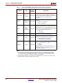
Certain pins are dedicated to configuration, while others are dual-purpose (Table 1-2).
Dual-purpose pins serve both as configuration pins and as user I/O after configuration.
Dedicated configuration pins retain their function after configuration.
Table 1-2:
Virtex-4 Configuration Pins
Type (1)
Dedicated or
Dual-Purpose (2)
M[2:0]
Input
Dedicated
Mode pins that determine configuration mode. Sampled on the rising
edge of INIT_B.
CCLK
Input or
Output
Dedicated
Configuration clock source for all configuration modes except JTAG.
D_IN
Input
Dedicated
Serial data input for serial configuration modes.
Output
Dedicated
In Serial configuration mode, pin acts as serial data output for daisy-chain
configuration. In SelectMAP mode, pin acts as BUSY output.
Bidirectional,
Open-Drain
or Active
Dedicated
Active High signal indicating configuration is complete.
0 = FPGA not configured
1 = FPGA configured
Pin Name
DOUT_BUSY
DONE
Description
Refer to the “BitGen” section of the Development System Reference Guide for
software settings.
INIT_B
PROGRAM_B
SelectMAP
Data
Input or
Output,
Open-Drain
Dedicated
Before MODE pins are sampled, INIT_B is an input that can be held Low
to delay configuration.
After MODE pins are sampled, INIT_B is an open-drain active Low
output indicating whether a CRC error occurred during configuration:
0 = CRC error
1 = No CRC error
Input
Dedicated
Active Low asynchronous full-chip reset.
Bidirectional
Dual-Purpose
Parallel data inputs for SelectMAP modes.
For 8-bit SelectMAP:
D0 = MSB
D7 = LSB
For 32-bit SelectMAP:
D0 = LSB
D31 = MSB
14
www.xilinx.com
Virtex-4 FPGA Configuration User Guide
UG071 (v1.11) June 9, 2009
R
Table 1-2:
Setup (Steps 1-3)
Virtex-4 Configuration Pins (Continued)
Pin Name
HSWAPEN
Type (1)
Dedicated or
Dual-Purpose (2)
Input
Dedicated
Description
Active High input used to disable weak pre-configuration I/O pull-up
resistors:
0 = weak pre-configuration I/O pull-up resistors enabled
1 = weak pre-configuration I/O pull-up resistors disabled
HSWAPEN must be connected to either enable or disable the pull-up
resistors.
HSWAPEN has a weak pull-up prior to and during configuration. The
weak pull-up does not always provide a reliable 1.
Notes:
1. The Bidirectional type describes a pin that is bidirectional under all conditions. If the pin is an input for some configuration modes or an
output for others, it is listed as an Input or Output type.
2. Dual-purpose pins can become user I/O after configuration. See “PERSIST” in Chapter 7 for details.
Setup (Steps 1-3)
While each of the configuration interfaces is different, the basic steps for configuring a
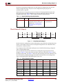
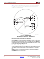
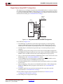
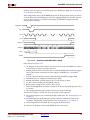
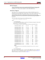
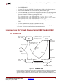
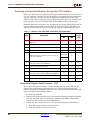
Virtex-4 device are the same for all modes. Figure 1-1 shows the Virtex-4 configuration
process. Each step is described in detail in the following sections.
Steps
1
2
3
Device
Power-Up
Clear
Configuration
Memory
Sample Mode
Pins
4
5
6
Synchronization
Device ID
Check
Load
Configuration
Data
7
8
CRC Check
Startup
Sequence
Bitstream
Loading
Start
Finish
ug071_01_122105
Figure 1-1:
Virtex-4 Configuration Process
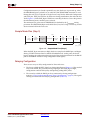
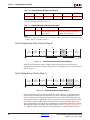
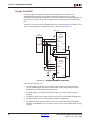
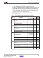
Device Power-Up (Step 1)
Steps
1
2
Device
Power-Up
Clear
Configuration
Memory
3
Sample Mode
Pins
4
Synchronization
5
6
7
8
Device ID
Check
Load
Configuration
Data
CRC Check
Startup
Sequence
Bitstream
Loading
Start
Finish
ug071_02_122105
Figure 1-2:
Device Power-Up (Step 1)
For configuration, Virtex-4 devices require power on the VCC_CONFIG, VCCAUX, and
VCCINT pins. There are no power-supply sequencing requirements.
All JTAG and serial configuration pins are located in a separate, dedicated bank with a
dedicated VCC_CONFIG (VCCO_0) supply. The SelectMAP data pins are shared dualpurpose pins, and are located in Bank 2 (VCCO_2). All dedicated input pins operate at
VCC_CONFIG LVCMOS level. All active dedicated output pins operate at the VCC_CONFIG
voltage level with the output standard set to LVCMOS_12F. In SelectMAP mode, VCCO_2
must be connected to the appropriate voltage to match the I/O standard of the
configuration device.
Virtex-4 FPGA Configuration User Guide
UG071 (v1.11) June 9, 2009
www.xilinx.com
15
R
Chapter 1: Configuration Overview
For power-up, the VCCINT power pins must be supplied with a 1.2V source. None of the
I/O voltage supplies (VCCO), except VCCO_0 (VCC_CONFIG), need to be powered for
Virtex-4 configuration in JTAG or serial modes. Table 1-3 shows the power supplies
required for configuration; for recommended operating conditions, see Table 2 of the
Virtex-4 FPGA Data Sheet. Table 41 of the Virtex-4 FPGA Data Sheet shows the configuration
power-up timing parameters. Table 7-1 shows the number of frames per Virtex-4 device.
Table 1-3:
Power Supplies Required for Configuration
Pin Name
VCCINT
VBATT
Description
Internal core voltage relative to GND.
(1)
Encryption Key battery supply.
VCC_CONFIG
Configuration output supply voltage (also known as VCCO_0)
VCCAUX
Auxiliary power input for configuration logic and other FPGA functions.
Notes:
1. VBATT is required only when using bitstream encryption.
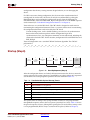
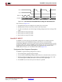
TPOR
VCC
PROGRAM_B
TPL
INIT_B
TTICCK
CCLK Output or Input
M0, M1, M2*
(Required)
VALID
*Can be either 0 or 1, but must not toggle during and after configuration.
ug071_03_073007
Figure 1-3:
Device Power-Up Timing
VCCINT should rise monotonically within the specified ramp rate. If this is not possible,
delay configuration by holding the INIT_B pin or the PROGRAM_B pin Low (see
“Delaying Configuration”) while the system power reaches VPOR.
The configuration logic power input (VCC_CONFIG) and the auxiliary voltage input
(VCCAUX) are used as a logic input to the Power-On-Reset (POR) circuitry. If either of these
voltage planes dips below the specified level, POR can trigger.
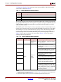
Clear Configuration Memory (Step 2, Initialization)
Steps
1
2
3
Device
Power-Up
Clear
Configuration
Memory
Sample Mode
Pins
4
5
6
Synchronization
Device ID
Check
Load
Configuration
Data
Bitstream
Loading
Start
7
8
CRC Check
Startup
Sequence
Finish
ug071_04_122105
Figure 1-4:
16
www.xilinx.com
Initialization (Step 2)
Virtex-4 FPGA Configuration User Guide
UG071 (v1.11) June 9, 2009
R
Setup (Steps 1-3)
Configuration memory is cleared sequentially any time the device is powered up, when
the PROGRAM_B pin is pulsed Low, or when the JTAG JPROGRAM instruction is used.
During this time, I/Os are placed in a high-Z state except for the dedicated Configuration
and JTAG pins. INIT_B is held Low by the device during initialization, then released after
TPOR (Figure 1-3.) If the INIT_B pin is held Low externally, the device waits at this point in
the initialization process until the pin is released.
The minimum Low pulse time for PROGRAM_B is defined by the TPROGRAM timing
parameter. The PROGRAM_B pin can be held active (Low) for as long as necessary, and the
device remains held in the reset state.
Sample Mode Pins (Step 3)
Steps
1
2
3
Device
Power-Up
Clear
Configuration
Memory
Sample Mode
Pins
4
5
6
Synchronization
Device ID
Check
Load
Configuration
Data
Bitstream
Loading
Start
7
CRC Check
8
Startup
Sequence
Finish
ug071_05_122105
Figure 1-5: Sample Mode Pins (Step 3)
When the INIT_B pin transitions to High, the device samples the MODE pins and begins
driving CCLK if in Master Serial or Master SelectMAP mode. At this point, the device
begins sampling the configuration data input pins (DIN pin for Serial Modes or the D0–D7
pins for SelectMAP modes on rising configuration clock signals).
Delaying Configuration
There are two ways to delay configuration for Virtex-4 devices:
•
The first is to hold the INIT_B pin Low during initialization (Figure 1-3). This method
only works if INIT_B is prevented from going High. After INIT_B goes High,
configuration cannot be delayed by subsequently pulling INIT_B Low.
•
The second is to hold the PROG pin Low, continuously clearing configuration
memory (“Clear Configuration Memory (Step 2, Initialization),” page 16). The signals
relating to initialization and delaying configuration (Table 1-4).
Virtex-4 FPGA Configuration User Guide
UG071 (v1.11) June 9, 2009
www.xilinx.com
17
R
Chapter 1: Configuration Overview
Table 1-4:
Signals Relating to Initialization and Delaying Configuration
Signal Name
PROGRAM_B
INIT_B
Type (1)
Access (2)
Input
Externally accessible via
the PROGRAM_B pin.
Global asynchronous chip reset.
Can be held Low to delay
configuration.
Input or
Output
Externally accessible via
the INIT_B pin.
Before the MODE pins are
sampled, INIT_B is an input that
can be held Low to delay
configuration.
After the MODE pins are sampled,
INIT_B is an open-drain active
Low output indicating whether a
CRC error occurred during
configuration:
0 = CRC error
1 = No CRC error
Description
INIT_COMPLETE
Status
Internal signal,
accessible through the
Virtex-4 status register.
Indicates whether INIT_B signal
has been internally released.
MODE_STATUS[2:0]
Status
Internal signals,
accessible through the
Virtex-4 status register.
Reflects the values sampled on the
MODE pins when INIT_B is
asserted High.
Notes:
1. The Status type symbolizes an internal status signal without a corresponding pin.
2. Information on the Virtex-4 status register is available in Table 7-9. Information on accessing the
JTAG capture sequence is available in Table 8-4.
Bitstream Loading (Steps 4-7)
The bitstream loading process is similar for all configuration modes; the primary
difference between modes is the interface to the configuration logic. Details on the different
configuration interfaces are provided in Chapter 2.
The most important steps in the bitstream loading process are, synchronization, device ID
check, loading configuration data, and the CRC check. Each of these steps involves distinct
parts of the configuration bitstream. The steps prior to synchronization and after the CRC
check do not directly involve the configuration bitstream.
Synchronization (Step 4)
Steps
1
Device
Power-Up
2
Clear
Configuration
Memory
3
4
5
Sample Mode
Pins
Synchronization
Device ID
Check
6
Load
Configuration
Data
Bitstream
Loading
Start
7
8
CRC Check
Startup
Sequence
Finish
ug071_06_122105
Figure 1-6:
Synchronization (Step 4)
Before the configuration data frames can be loaded, a special 32-bit synchronization word
(0xAA995566) must be sent to the configuration logic. The synchronization word alerts
18
www.xilinx.com
Virtex-4 FPGA Configuration User Guide
UG071 (v1.11) June 9, 2009
R
Bitstream Loading (Steps 4-7)
the device to upcoming configuration data and aligns the configuration data with the
internal configuration logic. Any data on the configuration input pins prior to
synchronization is ignored.
Synchronization is transparent to most users because all configuration bitstreams (.bit
files) generated by the Xilinx ISE® Bitstream Generator (BitGen) software include the
synchronization word. Table 1-5 shows signals relating to synchronization.
Table 1-5:
Signals Relating to Synchronization
Signal Name
Type
DALIGN
Status
Access
Description
Indicates whether device
is synchronized.
Only available through the
SelectMAP interface during an
ABORT. (See “Configuration
Abort Sequence Description,”
page 49.)
Check Device ID (Step 5)
Steps
1
2
3
Device
Power-Up
Clear
Configuration
Memory
Sample Mode
Pins
4
5
6
Synchronization
Device ID
Check
Load
Configuration
Data
7
8
CRC Check
Startup
Sequence
Bitstream
Loading
Start
Finish
ug071_07_122105
Figure 1-7:
Check Device ID (Step 5)
Once the device is synchronized, a device ID check must pass before the configuration data
frames can be loaded. This prevents an attempted configuration with a bitstream that is
formatted for a different device.
For example, the device ID check should prevent an XC4VLX15 from being configured
with an XC4VLX80 bitstream.
The device ID check is built into the bitstream, making this step transparent to most
designers. Figure 1-7 shows the relative position of the device ID check, Table 1-6 shows
the Virtex-4 device IDs, and Table 1-7 shows the signals relating to the device ID check. The
device ID check is performed through commands in the bitstream to the configuration
logic, not through the JTAG IDCODE register in this case.
Table 1-6:
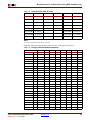
Virtex-4 Device ID Codes
Device
IDCODE
XC4VLX15
01658093
XC4VLX25
0167C093
XC4VSX25
XC4VLX40
016A4093
XC4VLX60
016B4093
XC4VLX80
016D8093
XC4VLX100
XC4VLX160
Virtex-4 FPGA Configuration User Guide
UG071 (v1.11) June 9, 2009
Device
Device
IDCODE
XC4VFX12
01E58093
02068093
XC4VFX20
01E64093
XC4VSX35
02088093
XC4VFX40
01E8C093 (1)
XC4VSX55
020B0093
XC4VFX60
01EB4093
01700093
XC4VFX100
01EE4093
01718093
XC4VFX140
01F14093
www.xilinx.com
IDCODE
19
R
Chapter 1: Configuration Overview
Table 1-6:
Virtex-4 Device ID Codes (Continued)
Device
IDCODE
Device
XC4VLX200
01734093
IDCODE
Device
IDCODE
Notes:
1. Does not reflect the actual device array size.
Table 1-7:
Signals Relating to the Device ID Check
Signal Name
Type
ID_Err
Status
Access (1)
Description
Internal signal. Accessed
only through the Virtex-4
status register.
Indicates a mismatch between the
device ID specified in the bitstream
and the actual device ID.
Notes:
1. Information on the Virtex-4 status register is available in Table 7-9. Information on accessing the JTAG
capture sequence is available in Table 8-4.
Load Configuration Data Frames (Step 6)
Steps
1
2
3
Device
Power-Up
Clear
Configuration
Memory
Sample Mode
Pins
4
5
6
Synchronization
Device ID
Check
Load
Configuration
Data
7
8
CRC Check
Startup
Sequence
Bitstream
Loading
Start
Finish
ug071_08_122105
Figure 1-8:
Load Configuration Data Frames (Step 6)
After the synchronization word is loaded and the device ID has been checked, the
configuration data frames are loaded. This process is transparent to most users. For details,
refer to Chapter 7
Cyclic Redundancy Check (Step 7)
Steps
1
2
3
Device
Power-Up
Clear
Configuration
Memory
4
Sample Mode
Pins
Synchronization
5
6
7
8
Device ID
Check
Load
Configuration
Data
CRC Check
Startup
Sequence
Bitstream
Loading
Start
Finish
ug071_09_122105
Figure 1-9:
Cyclic Redundancy Check (Step 7)
As the configuration data frames are loaded, the device calculates a Cyclic Redundancy
Check (CRC) value from the configuration data packets. After the configuration data
frames are loaded, the configuration bitstream can issue a Check CRC instruction to the
device, followed by an expected CRC value. If the CRC value calculated by the device does
not match the expected CRC value in the bitstream, the device pulls INIT_B Low and
aborts configuration. The CRC check is included in the configuration bitstream by default,
although the designer can disable it if desired. (Refer to the Development System Reference
Guide, BitGen section.) If the CRC check is disabled, there is a risk of loading incorrect
20
www.xilinx.com
Virtex-4 FPGA Configuration User Guide
UG071 (v1.11) June 9, 2009
R
Startup (Step 8)
configuration data frames, causing incorrect design behavior, or even damaging the
device.
If a CRC error occurs during configuration, the device must be resynchronized and
reconfigured. In serial modes, the device can only be resynchronized by pulsing the
PROGRAM_B pin and restarting the configuration process from the beginning. In
SelectMAP modes, either the PROGRAM_B pin can be pulsed Low or an ABORT sequence
can be initiated (see “SelectMAP Configuration Interface” in Chapter 2).
Virtex-4 devices use a 32-bit CRC check. The CRC check is designed to catch errors in
transmitting the configuration bitstream. There is a scenario where errors in transmitting
the configuration bitstream can be missed by the CRC check:
Certain clocking errors, such as double-clocking, can cause loss of synchronization
between the 32-bit bitstream packets and the configuration logic. Once
synchronization is lost, any subsequent commands are not understood, including the
command to check the CRC. In this situation, configuration fails with DONE Low and
INIT_B High.
Virtex-4 configuration uses a standard CRC32C checksum algorithm. The CRC32C
polynomial is:
x
32
+x
28
+x
27
+x
26
+x
25
+x
23
+x
22
+x
20
+x
19
+x
18
+x
14
+x
13
+x
11
+x
10
9
8
6
+x +x +x +1
Startup (Step 8)
Steps
1
2
Device
Power-Up
Clear
Configuration
Memory
3
Sample Mode
Pins
4
Synchronization
5
6
7
8
Device ID
Check
Load
Configuration
Data
CRC Check
Startup
Sequence
Bitstream
Loading
Start
Finish
ug071_10_122105
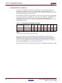
Figure 1-10:
Start-Up Sequence (Step 8)
After the configuration frames are loaded, the bitstream instructs the device to enter the
startup sequence. The startup sequence is controlled by an 8-phase (phases 0–7) sequential
state machine. The startup sequencer performs the tasks outlined in Table 1-8.
Table 1-8:
User-Selectable Cycle of Startup Events
Phase
Event
1–6
Wait for DCMs to Lock (optional)
1–6
Wait for DCI to Match (optional)
1–6
Assert GWE (Global Write Enable), allowing RAMs and flip-flops to change state
1–6
Negate GTS (Global 3-State), activating I/O
1–6
Release DONE pin
7
Assert EOS (End Of Startup)
The specific order of startup events (except for EOS assertion) is user-programmable
through BitGen options (refer to the Development System Reference Guide). Table 1-8 shows
the general sequence of events, although the specific phase for each of these startup events
is user-programmable (EOS is always asserted in the last phase). Refer to Chapter 2,
Virtex-4 FPGA Configuration User Guide
UG071 (v1.11) June 9, 2009
www.xilinx.com
21
R
Chapter 1: Configuration Overview
“Configuration Interfaces” for important startup option guidelines. By default, startup
events occur as shown in Table 1-9.
Table 1-9:
Default Sequence of Startup Events
Phase
Event
4
Release DONE pin
5
Negate GTS, activating I/O
6
Assert GWE, allowing RAMs and FFs to change state
7
Assert EOS
The start-up sequence can be forced to wait for the DCMs to lock or for DCI to match with
the appropriate BitGen options. These options are typically set to prevent DONE, GTS, and
GWE from being asserted (preventing device operation) before the DCMs have locked
and/or DCI has matched.
The DONE signal is released by the start-up sequencer on the cycle indicated by the user,
but the start-up sequencer does not proceed until the DONE pin actually sees a logic High.
The DONE pin is an open-drain bidirectional signal by default. By releasing the DONE
pin, the device simply stops driving a logic Low and the pin goes into a high-Z state. An
external pull-up resistor is needed for the DONE pin to reach a logic High in this case.
Table 1-10 shows signals relating to the status register. Figure 1-11 shows the signals
relating to the start-up sequencer.
Table 1-10:
Signals Relating to Status Register
Signal Name
DONE
Type
Access (1)
Description
Bidirectional (2)
DONE pin or
Virtex-4 Status
Register
Indicates configuration is complete. Can be
held Low externally to synchronize startup
with other FPGAs.
Release_DONE
Indicates whether device has released
DONE pin. If pin is held Low externally,
Release_DONE can differ from actual value
on DONE pin.
GWE
Global Write Enable. When de asserted GWE
disables CLB and IOB flips-flops as well as
other synchronous elements on the FPGA.
GTS
Global Tri-State. When asserted, GTS
disables all the I/O drivers except for
configuration pins.
Virtex-4
EOS
Status
Status
Register
End of Startup. EOS indicates the absolute
end of the configuration and startup process.
DCI_MATCH
DCI_MATCH indicates when all the
Digitally Controlled Impedance (DCI)
controllers have matched their internal
resistor to the external reference resistor.
DCM_LOCK
DCM_LOCK indicates when all the Digital
Clock Managers (DCMs) have locked. This
signal is asserted by default. It is active if the
LOCK_WAIT option is used on a DCM and
the LockCycle option is used when the
bitstream is generated.
Notes:
1. Information on the Virtex-4 status register is available in Table 7-9. Information on accessing the JTAG
capture sequence is available in Table 8-4.
2. Open-drain output by default; optional driver enabled using BitGen drivedone option.
22
www.xilinx.com
Virtex-4 FPGA Configuration User Guide
UG071 (v1.11) June 9, 2009
R
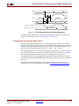
Bitstream Encryption
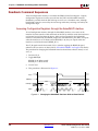
POR
INIT_B
DONE
GWE
GTS
EOS
CCLK
Initialization
Figure 1-11:
Configuration
End of Bitstream
Startup
ug071_11_080305
Configuration Signal Sequencing (Default Startup Settings)
Bitstream Encryption
Virtex-4 devices have on-chip AES (Advanced Encryption Standard) decryption logic to
provide a high degree of design security. Without knowledge of the encryption key,
potential pirates cannot analyze an externally intercepted bitstream to understand or clone
the design. Encrypted Virtex-4 designs cannot be copied or reverse-engineered.
The Virtex-4 AES system consists of software-based bitstream encryption and on-chip
bitstream decryption with dedicated memory for storing the encryption key. Using the
Xilinx ISE software, the user generates the encryption key and the encrypted bitstream.
During configuration, the Virtex-4 device performs the reverse operation, decrypting the
incoming bitstream. The Virtex-4 AES encryption logic uses a 256-bit encryption key.
The on-chip AES decryption logic cannot be used for any purpose other than bitstream
decryption; i.e., the AES decryption logic is not available to the user design and cannot be
used to decrypt any data other than the configuration bitstream.
Virtex-4 devices store the encryption key internally in dedicated RAM, backed up by a
small externally connected battery. The encryption key can only be programmed onto the
device through the JTAG interface; once programmed, it is not possible to read the
encryption key out of the device through JTAG or any other means.
ICAP is not supported with an encrypted bitstream in the LX, SX, and FX12 devices.
AES Overview
The Virtex-4 encryption system uses the Advanced Encryption Standard (AES) encryption
algorithm. AES is an official standard supported by the National Institute of Standards and
Technology (NIST) and the U.S. Department of Commerce
(http://csrc.nist.gov/publications/fips/fips197/fips-197.pdf).
The Virtex-4 AES encryption system uses a 256-bit encryption key (the alternate key
lengths of 128- and 192- bits described by NIST are not implemented) to encrypt or decrypt
blocks of 128 bits of data at a time. According to NIST, there are 1.1 x 1077 possible key
combinations for a 256-bit key.
Symmetric encryption algorithms such as AES use the same key for encryption and
decryption. The security of the data is therefore dependent on the secrecy of the key.
Virtex-4 FPGA Configuration User Guide
UG071 (v1.11) June 9, 2009
www.xilinx.com
23
R
Chapter 1: Configuration Overview
Creating an Encrypted Bitstream
The Xilinx Bitstream Generator (BitGen, provided with the Xilinx ISE software) can
generate encrypted as well as non-encrypted bitstreams. For AES bitstream encryption, the
user specifies a 256-bit key as an input to BitGen. BitGen in turn generates an encrypted
bitstream file (.bit) and an encryption key file (.nky).
For specific BitGen commands and syntax, refer to the Development System Reference Guide.
Loading the Encryption Key
The encryption key can only be programmed onto a Virtex-4 device through the JTAG
interface. The iMPACT tool, provided with the Xilinx ISE software, can accept the .nky file
as an input and program the device with the key through JTAG, using a supported Xilinx
programming cable.
To program the key, the device enters a special key-access mode using the ISC_PROGRAM
instruction, as detailed in the JTAG 1532 specification. In this mode, all FPGA memory,
including the encryption key and configuration memory, is cleared. Once the key is
programmed and the key-access mode is exited, it cannot be read out of the device by any
means, and it cannot be reprogrammed without clearing the entire device. The key-access
mode is transparent to most users.
Loading Encrypted Bitstreams
Once the device has been programmed with the correct encryption key, the device can be
configured with an encrypted bitstream. After configuration with an encrypted bitstream,
it is not possible to read the configuration memory through JTAG or SelectMAP readback,
regardless of the BitGen security setting.
After loading the encryption key, a non-encrypted bitstream can be used to configure the
device; in this case the key is ignored. After configuring with a non-encrypted bitstream,
readback is possible (if allowed by the BitGen security setting). The encryption key still
cannot be read out of the device, preventing the use of Trojan Horse bitstreams to defeat the
Virtex-4 encryption scheme.
However, once an encrypted bitstream has been used to configure a device, the device
cannot be reconfigured with a non-encrypted bitstream unless a full-chip reset is
performed first by pulling the PROGRAM_B pin Low, cycling power, or issuing a
JPROGRAM instruction. Additional encrypted reconfigurations can be performed.
The method of configuration is not affected by encryption. The configuration bitstream can
be delivered in any mode (Serial, SelectMAP, or JTAG) from any configuration solution
(PROM, System ACE™ tool, etc.). Configuration timing and signaling are unaffected by
encryption.
The encrypted bitstream must configure the entire device, because partial reconfiguration
through the external configuration interfaces is not permitted for encrypted bitstreams.
After configuration, the device cannot be reconfigured without toggling the PROG pin,
cycling power, or issuing the JTAG JSTART or JPROG instruction. Readback is available
through the ICAP primitive (see “Bitstream Encryption and Internal Configuration Access
Port (ICAP)”). None of these events resets the key if VBATT or VCCAUX is maintained.
24
www.xilinx.com
Virtex-4 FPGA Configuration User Guide
UG071 (v1.11) June 9, 2009
R
Bitstream Encryption
A mismatch between the key in the encrypted bitstream and the key stored in the device
causes configuration to fail with the INIT pin remaining High and the DONE pin
remaining Low. A mismatch between the key and bitstream can result in a high current on
VCCINT.
Note:
1.
Do not use or monitor BUSY when loading an encrypted bitstream.
2.
SelectMAP-32 mode is not supported with encrypted bitstreams.
Bitstream Encryption and Internal Configuration Access Port (ICAP)
The Internal Configuration Access Port (ICAP) primitive provides the user logic with
access to the Virtex-4 configuration interface. The ICAP interface is similar to the
SelectMAP interface, although the restrictions on readback and reconfiguration for the
SelectMAP interface do not apply to the ICAP interface after configuration. Users can
perform readback and reconfiguration through the ICAP interface even if bitstream
encryption is used. Unless the designer wires the ICAP interface to user I/O, this does not
offer attackers a method for defeating the Virtex-4 AES encryption scheme. ICAP is not
supported with an encrypted bitstream in the LX, SX, and FX12 devices.
Users concerned about the security of their design should not:
•
Wire the ICAP interface to user I/O
-or•
Not instantiate the ICAP primitive.
Like the other configuration interfaces, the ICAP interface does not provide access to the
key register.
VBATT
The encryption key memory cells are volatile and must receive continuous power to retain
their contents. During normal operation, these memory cells are powered by the auxiliary
voltage input (VCCAUX), although a separate VBATT power input is provided for retaining
the key after VCCAUX is removed. Because VBATT draws very little current (on the order of
nano amperes), a small watch battery is suitable for this supply. (To estimate the battery
life, refer to VBATT DC Characteristics in the Virtex-4 FPGA Data Sheet and the battery
specifications.) At less than a 100 nA load, the endurance of the battery should be limited
only by its shelf life.
VBATT does not draw any current and can be removed while VCCAUX is applied. VBATT
cannot be used for any purpose other than retaining the encryption keys when VCCAUX is
removed.
Virtex-4 FPGA Configuration User Guide
UG071 (v1.11) June 9, 2009
www.xilinx.com
25
R
Chapter 1: Configuration Overview
26
www.xilinx.com
Virtex-4 FPGA Configuration User Guide
UG071 (v1.11) June 9, 2009
R
Chapter 2
Configuration Interfaces
Virtex®-4 devices have three configuration interfaces. Each configuration interface
corresponds to one or more configuration modes, shown in Table 2-1. For detailed
interface timing information, see the Virtex-4 FPGA Data Sheet.
Table 2-1:
Configuration Interfaces and Corresponding Configuration Modes
Configuration Interface
Corresponding Configuration Mode(s)
Serial
Master Serial, Slave Serial
SelectMAP (8-bit or 32-bit)
Master SelectMAP, Slave SelectMAP
JTAG
JTAG
Serial Configuration Interface
In serial configuration modes, the FPGA is configured by loading one configuration bit per
CCLK cycle:
•
In Master serial mode, CCLK is an output.
•
In Slave serial mode, CCLK is an input.
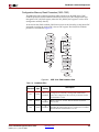
Figure 2-1 shows the basic Virtex-4 serial configuration interface.
There are four methods of configuring an FPGA in serial mode:
•
•
•
•
Master serial configuration
Slave serial configuration
Serial daisy chain configuration
Ganged serial configuration
Virtex-4 FPGA Configuration User Guide
UG071 (v1.11) June 9, 2009
www.xilinx.com
27
R
Chapter 2: Configuration Interfaces
M[2:0]
DOUT
D_IN
INIT_B
PROGRAM_B
DONE
CCLK
ug071_14_073007
Figure 2-1:
Virtex-4 Serial Configuration Interface
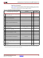
Table 2-2 describes the Serial Configuration Interface.
Table 2-2:
Virtex-4 Serial Configuration Interface Pins
Type
Dedicated
or DualPurpose
M[2:0]
Input
Dedicated
Mode Pins – determine configuration mode.
CCLK
Input or
Output
Dedicated
Configuration clock source for all configuration
modes except JTAG.
D_IN
Input
Dedicated
Serial configuration data input, synchronous to
rising CCLK edge.
Output
Dedicated
Serial data output for downstream daisy-chained
devices.
Pin Name
DOUT_BUSY
DONE
INIT_B
PROGRAM_B
28
Bidirectional,
open-drain
or active
Description
Active High signal indicating configuration is
complete:
Dedicated
0 = FPGA not configured
1 = FPGA configured
Refer to the “BitGen” section of the Development
System Reference Guide for software settings.
Input or
Output,
open-drain
Dedicated
Before the MODE pins are sampled, INIT_B is an
input that can be held Low to delay configuration.
After the MODE pins are sampled, INIT_B is an
open-drain active Low output indicating whether
a CRC error occurred during configuration:
0 = CRC error
1 = No CRC error
Input
Dedicated
Active-Low asynchronous full-chip reset.
www.xilinx.com
Virtex-4 FPGA Configuration User Guide
UG071 (v1.11) June 9, 2009
R
Serial Configuration Interface
Clocking Serial Configuration Data
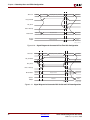
Figure 2-2 shows how configuration data are clocked into Virtex-4 devices in Slave serial
and Master serial modes.
PROGRAM_B
INIT_B
Master CLK Begins Here(2)
CCLK
BIT 0(1)
Master DIN
BIT 1
BIT n
BIT n+1
Master DOUT /
Slave DIN
BIT n-64
BIT n-63
Data bits clocked on rising edge of CCLK
DONE
ug071_016_073007
Figure 2-2:
Serial Daisy Chain Configuration Clocking Sequence
Notes relevant to Figure 2-2:
1.
In Figure 2-2, bit 0 represents the MSB of the first byte. For example, if the first byte is
0xAA (1010_1010), bit 0=1, bit 1=0, bit 2=1, etc.
2.
For Master configuration mode, CCLK does not transition until after MODE pins are
sampled, as indicated by the arrow.
3.
CCLK can be free-running in Slave serial mode.
Master Serial Configuration
The Master serial mode is designed so that the FPGA can be configured from a
Xilinx® serial configuration PROM, as shown in Figure 2-3.
M0
Xilinx
Serial PROM
M1
(7)
M2
DATA
DIN
CLK
DOUT
CCLK
CE
(7)
RESET/OE
(1)
Virtex-4
Master
Serial
(2)
PROGRAM_B
DONE
PROGRAM_B
UG071_12_073007
Figure 2-3:
Virtex-4 FPGA Configuration User Guide
UG071 (v1.11) June 9, 2009
INIT_B
Master Serial Mode Configuration
www.xilinx.com
29
R
Chapter 2: Configuration Interfaces
Notes relevant to Figure 2-3:
1.
The DONE pin is by default an open-drain output requiring an external pull-up
resistor. A 330Ω pull-up resistor is recommended. The DONE pin has a programmable
active driver. To enable it, enable the DriveDONE option in BitGen.
2.
The INIT_B pin is a bidirectional, open-drain pin. An external pull-up resistor is
required.
3.
The BitGen startup clock setting must be set for CCLK for serial configuration. The
oscillator frequency can be selected in BitGen (default is 4 MHz). Selectable
frequencies are 4, 5, 7, 8, 9, 10, 13, 15, 20, 26, 30, 34, 41, 45, 51, 55, and 60 MHz. Because
the oscillator can vary by ± 50%, select a maximum frequency not to exceed the FMAX
of the configuration device.
4.
The PROM in this diagram represents one or more Xilinx serial PROMs. Multiple serial
PROMs can be cascaded to increase the overall configuration storage capacity.
5.
The .bit file must be reformatted into a PROM file before it can be stored on the serial
PROM. Refer to the “Generating PROM Files” section.
6.
On XC17V00 PROMs, the reset polarity is programmable. RESET should be set for
active Low when using an XC17V00 device in this setup.
7.
Connect pull-up resistors to VCC_CONFIG (identical to VCC Bank 0).
8.
The CCLK net requires Thevenin parallel termination. See “Board Layout for
Configuration Clock (CCLK),” page 34.
9.
The CCLK pin is an output and an input.
Slave Serial Configuration
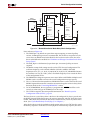
Slave serial configuration is typically used for devices in a serial daisy chain, or when
configuring a single device from an external microprocessor or CPLD. Design
considerations are similar to Master serial configuration except for the direction of CCLK.
A single device in Slave serial mode cannot simply be connected to a PROM, because
CCLK is an input on both devices.
Serial Daisy Chains
Multiple Virtex-4 devices can be configured from a single configuration source by
arranging the devices in a serial daisy chain. In a serial daisy chain, devices receive their
configuration data through their DIN pin, passing configuration data along to
downstream devices through their DOUT pin. The device closest to the configuration data
source is considered the most upstream device, while the device furthest from the
configuration data source is considered the most downstream device.
In a serial daisy chain, the configuration clock is typically provided by the most upstream
device in Master serial mode. All other devices are set for Slave serial mode. Figure 2-4
illustrates this configuration.
Alternatively, if a CPLD or microprocessor is used as a configuration controller, all devices
can be set for Slave serial mode. (See “Configuring a Serial Daisy Chain with a
Microprocessor or CPLD,” page 32.)
30
www.xilinx.com
Virtex-4 FPGA Configuration User Guide
UG071 (v1.11) June 9, 2009
R
Serial Configuration Interface
Xilinx
Serial PROM
(7)
M1
M0
M2
DATA
DOUT
DIN
CCLK
CE
(7)
M1
M2
DIN
CLK
RESET/OE
M0
DOUT
CCLK
Virtex-4
Master
Serial
(2)
Virtex-4
Slave
Serial
PROGRAM_B
PROGRAM_B
DONE
DONE
INIT_B
(1)
INIT_B
PROGRAM
ug071_17_073007
Figure 2-4:
Master/Slave Serial Mode Daisy Chain Configuration
Notes relevant to Figure 2-4:
1.
The DONE pin is by default an open-drain output requiring an external pull-up
resistor. A 330Ω pull-up resistor is recommended. For all devices except the last, the
active driver on DONE must be disabled. For the last device in the chain, the active
driver on DONE can be enabled. See “Guidelines and Design Considerations for Serial
Daisy Chains.”
2.
The INIT_B pin is a bidirectional, open-drain pin. An external pull-up resistor is
required.
3.
The BitGen startup clock setting must be set for CCLK for serial configuration. The
oscillator frequency can be selected in BitGen (default is 4 MHz). Selectable
frequencies are 4, 5, 7, 8, 9, 10, 13, 15, 20, 26, 30, 34, 41, 45, 51, 55, and 60 MHz. Because
the oscillator can vary by ± 50%, select a maximum frequency not to exceed the FMAX
of the configuration device.
4.
The PROM in this diagram represents one or more Xilinx serial PROMs. Multiple serial
PROMs can be cascaded to increase the overall configuration storage capacity.
5.
The .bit file must be reformatted into a PROM file before it can be stored on the serial
PROM. Separate bitstream files cannot be concatenated together to form a daisy-chain
bitstream. Refer to the “Generating PROM Files” section.
6.
On XC17V00 PROMs, the reset polarity is programmable. RESET should be set for
active Low when using an XC17V00 device in this setup.
7.
The CCLK net requires Thevenin parallel termination. See “Board Layout for
Configuration Clock (CCLK),” page 34.
The first device in a serial daisy chain is the first to be configured. No data is passed onto
the DOUT pin until all the data frames, the start-up command, and CRC check have been
loaded. CRC checks only include the data for the current device, not for any others in the
chain. (See “Cyclic Redundancy Check (Step 7)” in Chapter 1.)
After the first device in the chain finishes configuration and passes its CRC check, it enters
the Start-Up sequence. At the Release DONE pin phase in the Start-Up sequence, the device
Virtex-4 FPGA Configuration User Guide
UG071 (v1.11) June 9, 2009
www.xilinx.com
31
R
Chapter 2: Configuration Interfaces
places its DONE pin in a high-Z state while continuing to pass configuration data and
commands to downstream devices. After all devices release their DONE pins, the common
DONE signal is either pulled High externally or driven High by the last device in the chain.
On the next rising CCLK edge, all devices move out of the Release DONE pin phase and
complete their startup sequences.
It is important that all DONE pins in a Slave serial daisy chain be connected. Only the last
device in the serial daisy chain should have the DONE driver enabled. Enabling the DONE
driver on upstream devices causes contention on the DONE signal.
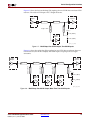
Configuring a Serial Daisy Chain with a Microprocessor or CPLD
If a microprocessor or CPLD is driving configuration instead of a Xilinx serial PROM, all
devices in the serial daisy chain can be set for Slave serial configuration mode, or the lead
FPGA can be set for Master serial, as shown in Figure 2-5.
Non-Xilinx
PROM (Parallel)
VCC
(6)
CPLD
ADDRESS[18:0]
DATAOUT[7:0]
CE
ADDRESS[18:0]
DATAIN
INIT_B
INIT_B
DOUT
DIN
CLKIN
CCLK
ROM_CS
LDC_DONE
OE
(6)
VCC
INIT_B
DOUT
DIN
CCLK
Virtex-4
Slave
Serial
Virtex-4
Master
Serial
DONE
DONE
PROGRAM_B
PROGRAM_B
VCC
Control Signal
ug071_18_073007
Figure 2-5: Serial Daisy Chain Configuration from Parallel EPROM and CPLD
Notes relevant to Figure 2-5:
32
1.
This schematic shows one of many possible implementations.
2.
The DONE pin is by default an open-drain output requiring an external pull-up
resistor. A 330Ω pull-up resistor is recommended. For all devices except the first, the
active driver on DONE must be disabled. For the first device in the chain, the active
driver on DONE can be enabled. See “Guidelines and Design Considerations for Serial
Daisy Chains.”
3.
The INIT_B pin is a bidirectional, open-drain pin. An external pull-up resistor is
required.
4.
The BitGen startup clock setting must be set for CCLK for serial configuration.
5.
The .bit file must be reformatted into a PROM file before it can be stored on the
PROM. Refer to the “Generating PROM Files” section.
6.
The CCLK net requires Thevenin parallel termination. See “Board Layout for
Configuration Clock (CCLK),” page 34.
www.xilinx.com
Virtex-4 FPGA Configuration User Guide
UG071 (v1.11) June 9, 2009
R
Serial Configuration Interface
Mixed Serial Daisy Chains
Virtex-4 devices can be daisy-chained with the Virtex, Spartan®-II, Virtex-E, Spartan-IIE,
Virtex-II, Virtex-II Pro, and Spartan-3 families. There are three important design
considerations when designing a mixed serial daisy chain:
•
Many older devices cannot accept as fast a CCLK frequency as a Virtex-4 device can
generate. Select a configuration CCLK speed supported by all devices in the chain.
•
Newer devices should be grouped at the beginning of the serial daisy chain, with
older devices located at the end of the chain.
•
The number of configuration bits that a device can pass through its DOUT pin is
limited. This limit varies for different families (Table 2-3). The sum of the bitstream
lengths for all downstream devices must not exceed the number in this table for each
family.
Table 2-3:
Maximum Number of Configuration Bits, Various Device Families
Architecture
Maximum DOUT Bits
Virtex-4
32 x( 227 – 1) = 4,294,967,264
Virtex-II Pro, Virtex-II
32 x( 227 – 1) = 4,294,967,264
Spartan-3
32 x (227 – 1) = 4,294,967,264
Virtex, Virtex-E, Spartan-II, Spartan-IIE
32 x (220 – 1) = 33,554,216
Guidelines and Design Considerations for Serial Daisy Chains
There are a number of important considerations for serial daisy chains:
Startup Sequencing (GTS)
GTS should be released before DONE or during the same cycle as DONE to ensure the
Virtex-4 device is operational when all DONE pins have been released.
Active DONE Driver
All devices except the first should disable the driver on the DONE pin (refer to the BitGen
section of the Development System Reference Guide for software settings):
•
DriveDone enabled (first device)
•
DriveDone disabled (all devices except the first)
Alternatively, the driver can be disabled for all DONE pins and an external pull-up resistor
added to pull the signal High after all devices have released it.
Connect All DONE Pins
It is important to connect the DONE pins for all devices in a serial daisy chain. Failing to
connect the DONE pins can cause configuration to fail. For debugging purposes, it is often
helpful to have a way of disconnecting individual DONE pins from the common DONE
signal, so that devices can be individually configured through the serial or JTAG interface.
DONE Pin Rise Time
After all DONE pins are released, the DONE pin should rise from logic 0 to logic 1 in one
CCLK cycle. If there are several devices in the serial daisy chain or other loads on the
DONE signal (such as LEDs or microprocessor inputs), external pull-up resistors can be
Virtex-4 FPGA Configuration User Guide
UG071 (v1.11) June 9, 2009
www.xilinx.com
33
R
Chapter 2: Configuration Interfaces
required. If additional time is required for the DONE signal to rise, the BitGen donepipe
option can be set for all devices in the serial daisy chain. (Refer to the BitGen section of the
Development System Reference Guide for software settings.)
Board Layout for Configuration Clock (CCLK)
The Virtex-4 output standard for all configuration I/Os, including CCLK, is different from
previous Xilinx FPGAs. To improve performance, the Virtex-4 configuration I/Os use the
LVCMOS fast slew rate standard of 12 mA. This change results in faster edge rates to
support higher configuration frequencies. This requires more attention to PCB trace
routing and termination for proper signal integrity.
These basic guidelines must be followed:
•
Route the CCLK net as a 50Ω controlled impedance transmission line.
•
Always route the CCLK net without any branching, do not use a star topology
(Figure 2-9).
•
Stubs, if necessary, must be shorter than 8 mm (0.3 inches).
•
Terminate the end of the CCLK transmission line with a parallel termination of 100Ω
to VCCO, and 100Ω to GND (the Thevenin equivalent of VCCO/2, and assuming a
trace characteristic impedance of 50Ω).
Xilinx recommends simulating the CCLK distribution with an IBIS simulator (such as
HyperLynx) to check for glitches on each CLK input, including the CCLK of the master
FPGA.
Figure 2-6 through Figure 2-8 show the recommended topologies for CCLK distribution.
Figure 2-6 shows the basic point-to-point topology for one CCLK driver (FPGA master)
and one CCLK receiver (PROM or FPGA slave).
CCLK
Input
CCLK
Output
Z0 (50 Ω)
Z0 (50 Ω)
VCCO_0
2 x Z0 (100 Ω)
CCLK Output = Master FPGA
CCLK Input = PROM or Slave FPGA
2 x Z0 (100 Ω)
ug071_2_06_072505
Figure 2-6:
34
Point-to-Point: One CCLK Output, One CCLK Input
www.xilinx.com
Virtex-4 FPGA Configuration User Guide
UG071 (v1.11) June 9, 2009
R
Serial Configuration Interface
Figure 2-7 shows the basic multi-drop flyby topology for one CCLK driver and two CCLK
receivers. The stub at CCLK input 1 has a length constraint.
CCLK
Input 2
CCLK
Output
Z0 (50 Ω)
Z0 (50 Ω)
Z0 (50 Ω)
length < 8mm
Z0 (50 Ω)
VCCO_0
2 x Z0 (100 Ω)
CCLK
Input 1
2 x Z0 (100 Ω)
ug071_2_07_072505
Figure 2-7:
Multi-Drop: One CCLK Output, Two CCLK Inputs
Figure 2-8 shows the multi-drop flyby topology for one CCLK driver and more than two
CCLK receivers (four in this example). All CCLK inputs except input 4 have length
constraints.
CCLK
Input 4
CCLK
Output
Z0 (50 Ω)
Z0 (50 Ω)
Z0 (50 Ω)
Z0 (50 Ω)
Z0 (50 Ω)
Z0 (50 Ω)
length < 8mm
Z0 (50 Ω)
length < 8mm
Z0 (50 Ω)
length < 8mm
VCCO_0
2 x Z0 (100 Ω)
CCLK
Input 1
CCLK
Input 2
CCLK
Input 3
2 x Z0 (100 Ω)
ug071_2_08_072505
Figure 2-8:
Multi-Drop: One CCLK Output, More Than Two CCLK Inputs
Virtex-4 FPGA Configuration User Guide
UG071 (v1.11) June 9, 2009
www.xilinx.com
35
R
Chapter 2: Configuration Interfaces
Figure 2-9 shows a star topology where the transmission line branches to the multiple
CCLK inputs. The branch point creates a significant impedance discontinuity. This
arrangement is Not Recommended.
CCLK
Input 1
Impedance
Discontinuity
Z0
CCLK
Output
Z0
CCLK
Input 2
Z0
ug071_2_09_080204
Figure 2-9: Not Recommended
Star Topology: One CCLK Output, Two CCLK Inputs
Daisy-Chaining Virtex-4 with Earlier FPGA Generations
A serial daisy chain can include earlier generations of Xilinx FPGAs (Virtex-II, Virtex,
Spartan-II, 4000, etc.). In general, newer devices should appear upstream of older devices.
For example, a daisy chain consisting of a Virtex-4, a Virtex-II, a Virtex, and a 4000E device
should be arranged with the Virtex-4 device first in the chain, the Virtex-II device second,
the Virtex device third, and the 4000E device last.
BitGen Options for Mixed Daisy Chains
All Virtex-based device families have similar BitGen options. The guidelines provided for
Virtex-4 BitGen options should be applied to all Virtex-based devices in a serial daisy
chain.
If 4000-series devices are included in the daisy chain, it is important to set the BitGen
SyncToDONE option for the startup settings.
36
www.xilinx.com
Virtex-4 FPGA Configuration User Guide
UG071 (v1.11) June 9, 2009
R
Serial Configuration Interface
Maximum CCLK Rate Varies Between Xilinx Device Families
Older Xilinx device families require slower CCLK rates than Virtex-4 devices. For mixed
serial daisy chains, ensure the Master device does not toggle CCLK faster than the slowest
device can tolerate.
PROM File Considerations
The PROM file for a serial daisy chain is larger than the sum of all bitstreams due to
additional configuration instructions. See “Generating PROM Files.”
Ganged Serial Configuration
More than one device can be configured simultaneously from the same bitstream using a
ganged serial configuration setup (Figure 2-10). In this arrangement, the serial
configuration pins are tied together such that each device sees the same signal transitions.
One device is typically set for Master serial mode (to drive CCLK) while the others are set
for Slave serial mode. For ganged serial configuration, all devices must be identical.
Configuration can be driven from a configuration PROM or from an external configuration
controller.
Xilinx
Serial PROM
(8)
M0 M1
M2
DIN
DATA
CLK
DOUT
CCLK
CE
RESET/OE
(8)
(1)
Virtex-4
Master
Serial
(2)
PROGRAM_B
DONE
PROGRAM
INIT_B
M0 M1
M2
DIN
DOUT
CCLK
Virtex-4
Slave
Serial
PROGRAM_B
DONE
INIT_B
ug071_15_073007
Figure 2-10:
Ganged Serial Configuration
Notes relevant to Figure 2-10:
1.
For ganged serial configuration, the optional DONE driver must be disabled for all
devices if one device is set for Master mode, because each device might not start up on
exactly the same CCLK cycle. An external pull-up resistor is required in this case.
2.
The INIT_B pin is a bidirectional, open-drain pin. An external pull-up resistor is
required.
Virtex-4 FPGA Configuration User Guide
UG071 (v1.11) June 9, 2009
www.xilinx.com
37
R
Chapter 2: Configuration Interfaces
3.
The BitGen startup clock setting must be set for CCLK for serial configuration.
4.
The PROM in this diagram represents one or more Xilinx serial PROMs. Multiple serial
PROMs can be cascaded to increase the overall configuration storage capacity.
5.
The .bit file must be reformatted into a PROM file before it can be stored on the serial
PROM. Refer to the “Generating PROM Files” section.
6.
On XC17V00 devices, the reset polarity is programmable. RESET should be set for
active Low when using an XC17V00 device in this setup.
7.
For ganged serial configuration, all devices must be identical (same IDCODE) and
must be configured with the same bitstream.
8.
The CCLK net requires Thevenin parallel termination. See “Board Layout for
Configuration Clock (CCLK),” page 34.
There are a number of important considerations for ganged serial configuration:
Startup Sequencing (GTS)
GTS should be released before DONE or during the same cycle as DONE to ensure all
devices are operational when all DONE pins have been released.
Disable the Active DONE Driver On for All Devices
For ganged serial configuration, the active DONE driver must be disabled for all devices if
the DONE pins are tied together, because there can be variations in the startup sequencing
of each device. A pull-up resistor is therefore required on the common DONE signal.
-g DriveDone:no (BitGen option, all devices)
Connect All DONE Pins if Using a Master Device
It is important to connect the DONE pins for all devices in ganged serial configuration if
one FPGA is used as the Master device. Failing to connect the DONE pins can cause
configuration to fail for individual devices in this case. If all devices are set for Slave serial
mode, the DONE pins can be disconnected (if the external CCLK source continues toggling
until all DONE pins go High).
For debugging purposes, it is often helpful to have a way of disconnecting individual
DONE pins from the common DONE signal.
DONE Pin Rise Time
After all DONE pins are released, the DONE pin should rise from logic 0 to logic 1 in one
CCLK cycle. If additional time is required for the DONE signal to rise, the BitGen
donepipe option can be set for all devices in the serial daisy chain.
Configuration Clock (CCLK) as Clock Signal for Board Layout
The CCLK signal is an LVCMOS fast 12 mA driver (LVCMOS_P12.) Signal integrity issues
on the CCLK signal can cause configuration to fail. (Typical failure mode: DONE Low,
INIT_B High.) Therefore, careful attention to signal integrity, including signal integrity
simulation with IBIS, is recommended.
Signal Fanout
Special care must be taken in assuring good signal integrity when using ganged serial
configuration. Signal integrity simulation is recommended.
38
www.xilinx.com
Virtex-4 FPGA Configuration User Guide
UG071 (v1.11) June 9, 2009
R
SelectMAP Configuration Interface
PROM Files for Ganged Serial Configuration
PROM files for ganged serial configuration are identical to the PROM files used to
configure single devices. There are no special PROM file considerations.
SelectMAP Configuration Interface
The SelectMAP configuration interface (Figure 2-11) provides an 8-bit bidirectional
data-bus interface to the Virtex-4 configuration logic that can be used for both
configuration and readback. (For details, refer to Chapter 8)
CCLK is an output in Master SelectMAP mode; in Slave SelectMAP, CCLK is an input. One
or more Virtex-4 devices can be configured through the SelectMAP bus.
There are four methods of configuring an FPGA in SelectMAP mode:
•
•
•
•
Single device Master SelectMAP
Single device Slave SelectMAP
Multiple device SelectMAP bus
Multiple device ganged SelectMAP
Table 2-4 describes the SelectMAP configuration interface.
M[2:0]
BUSY
SelectMap Data
INIT_B
PROGRAM_B
RDWR_B
CS_B
DONE
CCLK
ug071_21_073007
Figure 2-11:
Table 2-4:
Virtex-4 SelectMAP Configuration Interface
Virtex-4 SelectMAP Configuration Interface Pins
Type
Dedicated
or DualPurpose
M[2:0]
Input
Dedicated
MODE pins - determines configuration mode
CCLK
Input and
Output
Dedicated
Configuration clock source for all configuration
modes except JTAG
Pin Name
SelectMAP
Data
Virtex-4 FPGA Configuration User Guide
UG071 (v1.11) June 9, 2009
Three-State
Bidirectional
Dual
Purpose
www.xilinx.com
Description
Byte-wide (SelectMAP 8 bit) configuration and
readback data bus, clocked on rising edge of
CCLK. D0 is the most-significant bit (MSB), D7 the
least-significant bit (LSB). In SelectMAP 32 bit,
configuring the data order is straight D0 = LSB
and D31 = MSB.(1)
39
R
Chapter 2: Configuration Interfaces
Table 2-4:
Virtex-4 SelectMAP Configuration Interface Pins (Continued)
Pin Name
DOUT_BUSY
DONE
INIT_B
PROGRAM_B
CS_B
RDWR_B
Dedicated
or DualPurpose
Description
Dedicated
Indicates that the device is not ready to send
readback data. For Virtex-4 devices, the BUSY
signal is only needed for readback; it is not needed
for configuration (see “SelectMAP Data
Loading”).
Dedicated
Active High signal indicating configuration is
complete:
0 = FPGA not configured
1 = FPGA configured
Input or
Output,
Open-Drain
Dedicated
Before MODE pins are sampled, INIT_B is an
input that can be held Low to delay configuration.
After MODE pins are sampled, INIT_B is an opendrain active Low output indicating whether a CRC
error occurred during configuration:
0 = CRC error
1 = No CRC error
Input
Dedicated
Active-Low asynchronous full-chip reset
Dedicated
Active-Low chip select to enable the SelectMAP
data bus (see “SelectMAP Data Loading”):
0 = SelectMAP data bus enabled
1 = SelectMAP data bus disabled(2)
Type
Three-State
Output
Bidirectional,
Open-Drain
or active
Input
Input
Dedicated
Determines the direction of the SelectMAP data
bus (see “SelectMAP Data Loading”):
0 = inputs
1 = outputs
RDWR_B input can only be changed while CS_B is
deasserted, otherwise an ABORT occurs (see
“SelectMAP ABORT”)(2).
Notes:
1. If SelectMAP32 is used and the bitstream is compressed by the -g compress in BitGen then the
CONFIG_MODE constraint must be used. the values for the CONFIG_MODE constraint are either
S_SelectMAP32 or S_SelectMAP32+READBACK. S_SelectMAP32+READBACK preserves the
S_SelectMAP32 data pins for readback (also known as persist).
2. If the SelectMAP interface is not used, the CS_B and RDWR_B pins can be left unconnected. Weak
pullups pull these pins High, and their state is ignored.
40
www.xilinx.com
Virtex-4 FPGA Configuration User Guide
UG071 (v1.11) June 9, 2009
R
SelectMAP Configuration Interface
Single Device SelectMAP Configuration
The simplest way to configure a single device in SelectMAP mode is to connect it directly
to a parallel configuration PROM as shown in Figure 2-12. In this arrangement, the device
is set for Master SelectMAP mode, and the RDWR_B and CS_B pins are tied to Ground for
continuous data loading (see “SelectMAP Data Loading”).
Virtex-4
Master
SelectMAP
M0
M1
Xilinx
Serial PROM
M2
(10)
DATA[0:7]
D[0:7]
CCLK
CCLK
CF
PROGRAM_B
(10)
(1)
(2)
CE
DONE
RESET/OE
INIT_B
RDWR_B
CS_B
ug071_22_073007
Figure 2-12:
Single Device Master SelectMAP Configuration
Notes relevant to Figure 2-12:
1.
The DONE pin is by default an open-drain output requiring an external pull-up
resistor. A 330Ω pull-up resistor is recommended. In this arrangement, the active
DONE driver can be enabled, eliminating the need for an external pull-up resistor.
2.
The INIT_B pin is a bidirectional, open-drain pin. An external pull-up resistor is
required.
3.
The BitGen startup clock setting must be set for CCLK for SelectMAP configuration.
4.
The PROM in this diagram represents one or more Xilinx serial PROMs. Multiple serial
PROMs can be cascaded to increase the overall configuration storage capacity.
5.
The .bit file must be reformatted into a PROM file before it can be stored on the serial
PROM. Refer to the “Generating PROM Files” section.
6.
On XC17V00 devices, the reset polarity is programmable. RESET should be set for
active Low when using an XC17V00 device in this setup.
7.
The Xilinx PROM must be set for parallel mode. Note that this mode is not available
for all devices.
8.
When configuring a Virtex-4 device in SelectMAP mode from a Xilinx configuration
PROM, the RDWR_B and CS_B signals can be tied Low (see “SelectMAP Data
Loading”).
9.
The BUSY signal does not need to be monitored for this setup and can be left
unconnected (see “SelectMAP Data Loading”).
10. The CCLK net requires Thevenin parallel termination. See “Board Layout for
Configuration Clock (CCLK),” page 34.
11. The CCLK pin is an output and an input.
Virtex-4 FPGA Configuration User Guide
UG071 (v1.11) June 9, 2009
www.xilinx.com
41
R
Chapter 2: Configuration Interfaces
For custom applications where a microprocessor or CPLD is used to configure a single
Virtex-4 device, either Master or Slave SelectMAP mode can be used (Figure 2-13). See
Xilinx Application Note XAPP502 for information on configuring Virtex devices using a
microprocessor). Refer to the “Data Loading” section for details on handling the CS_B,
RDWR_B, and BUSY signals.
(7)
ADDRESS
PROGRAM_B
Program
Register
CS_B
RDWR_B
DATA
CCLK
D[0:7]
Config.
CPLD Register
CSO
Virtex-4
Slave
SelectMAP
(7)
CS1
(2)
WE
Input
Register
OE
(3)
INIT_B
DONE
Microprocessor
BUSY
Memory
Figure 2-13:
Used for storage
of the configuration
bitstream
ug071_19_073007
Single Slave Device SelectMAP Configuration
from Microprocessor and CPLD
Notes relevant to Figure 2-13:
1.
This schematic is from Xilinx Application Note XAPP502. It is one of many possible
implementations.
2.
The DONE pin is by default an open-drain output requiring an external pull-up
resistor. A 330Ω pull-up resistor is recommended. In this arrangement, the active
DONE driver can be enabled, eliminating the need for an external pull-up resistor.
3.
The INIT_B pin is a bidirectional, open-drain pin. An external pull-up resistor is
required.
4.
The BitGen startup clock setting must be set for CCLK for SelectMAP configuration.
5.
The BUSY signal can be left unconnected if readback is not needed.
6.
The CS_B and RDWR_B signals can be tied to ground if only one FPGA is going to be
configured and readback is not needed.
7.
The CCLK net requires Thevenin parallel termination. See “Board Layout for
Configuration Clock (CCLK),” page 34.
Multiple Device SelectMAP Configuration
Multiple Virtex-4 devices in Slave SelectMAP mode can be connected on a common
SelectMAP bus (Figure 2-14). In a SelectMAP bus, the data pins (SelectMAP data, CCLK,
RDWR_B, BUSY, PROGRAM_B, DONE, and INIT_B share a common connection between
all of the devices. To allow each device to be accessed individually, the CS_B (Chip Select)
inputs must not be tied together. External control of the CS_B signal is required and is
usually provided by a microprocessor or CPLD.
If Readback is going to be performed on the device after configuration, the RDWR_B and
BUSY signals must be handled appropriately. (For details, refer to Chapter 8)
42
www.xilinx.com
Virtex-4 FPGA Configuration User Guide
UG071 (v1.11) June 9, 2009
R
SelectMAP Configuration Interface
Otherwise, RDWR_B can be tied Low and BUSY can be ignored. Unlike earlier Virtex
devices, the BUSY signal never needs to be monitored when configuring Virtex-4 devices.
Refer to “Bitstream Loading (Steps 4-7)” in Chapter 1 and to Chapter 8.
(6)
DATA[0:7]
CCLK
WRITE
BUSY
(6)
M1
M2
M1
M0
Virtex-4
Slave
SelectMAP
Virtex-4
Slave
SelectMAP
D[0:7]
D[0:7]
CCLK
CCLK
RDWR_B
RDWR_B
BUSY
CS(0)
(1)
BUSY
CS(1)
CS_B
PROGRAM_B
(2)
M2
M0
DONE
INIT_B
CS_B
PROGRAM_B
DONE
INIT_B
DONE
INIT
PROGRAM
ug071_20_073007
Figure 2-14:
Multiple Slave Device Configuration on an 8-bit SelectMAP Bus
Notes relevant to Figure 2-14:
1.
The DONE pin is by default an open-drain output requiring an external pull-up
resistor. A 330Ω pull-up resistor is recommended. In this arrangement, the active
DONE driver must be disabled.
2.
The INIT_B pin is a bidirectional, open-drain pin. An external pull-up resistor is
required.
3.
The BitGen startup clock setting must be set for CCLK for SelectMAP configuration.
4.
The BUSY signals can be left unconnected if readback is not needed.
5.
An external controller such as a microprocessor or CPLD is needed to control
configuration.
6.
The CCLK net requires Thevenin parallel termination. See “Board Layout for
Configuration Clock (CCLK),” page 34.
Virtex-4 FPGA Configuration User Guide
UG071 (v1.11) June 9, 2009
www.xilinx.com
43
R
Chapter 2: Configuration Interfaces
Ganged SelectMAP
It is also possible to configure simultaneously multiple devices with the same
configuration bitstream by using ganged SelectMAP configuration. In a ganged
SelectMAP arrangement, the CS_B pins of two or more devices are connected together (or
tied to ground), causing all devices to recognize data presented on the SelectMAP data
pins.
All devices can be set for Slave SelectMAP mode if an external oscillator is available, or one
device can be designated as the Master device, as illustrated in Figure 2-15.
M1
Xilinx
Serial PROM
M2
M0
Virtex-4
SelectMAP
Master
DATA[0:7]
D[0:7]
CCLK
CCLK
PROGRAM_B
CF
BUSY
CE
RESET/OE
INIT_B
RDWR_B
(1)
CS_B
DONE
M1
M2
(10)
M0
Virtex-4
SelectMAP
Slave
D[0:7]
CCLK
PROGRAM_B
(2)
BUSY
INIT_B
(10)
RDWR_B
CS_B
DONE
ug071_24_073007
Figure 2-15:
Ganged SelectMAP Configuration
Notes relevant to Figure 2-15:
44
1.
The DONE pin is by default an open-drain output requiring an external pull-up
resistor. A 330Ω pull-up resistor is recommended. In this arrangement, the active
DONE driver must be disabled for both devices.
2.
The INIT_B pin is a bidirectional, open-drain pin. An external pull-up resistor is
required.
3.
The BitGen startup clock setting must be set for CCLK for SelectMAP configuration.
4.
The BUSY signal is not used for ganged SelectMAP configuration.
5.
The PROM in this diagram represents one or more Xilinx Platform Flash PROMs.
Multiple serial PROMs can be cascaded to increase the overall configurations storage
capacity.
www.xilinx.com
Virtex-4 FPGA Configuration User Guide
UG071 (v1.11) June 9, 2009
R
SelectMAP Configuration Interface
6.
The .bit file must be reformatted into a PROM file before it can be stored on the serial
PROM. Refer to the “Generating PROM Files” section.
7.
On 17V00 devices, the reset polarity is programmable. Reset should be set for active
Low when using a 17V00 device in this setup.
8.
The Xilinx PROM must be set for parallel mode. This mode is not available for all
devices.
9.
When configuring a Virtex-4 device in SelectMAP mode from a Xilinx configuration
PROM, the RDWR_B and CS_B signals can be tied Low (see “SelectMAP Data
Loading”).
10. The CCLK net requires Thevenin parallel termination. See “Board Layout for
Configuration Clock (CCLK),” page 34.
If one device is designated as the Master, the DONE pins of all devices must be connected
and with the active DONE drivers disabled. An external pull-up resistor is required on the
common DONE signal. Careful attention must be paid to signal integrity due to the
increased fanout of the outputs from the PROM. Signal integrity simulation is
recommended.
Readback is not possible if the CS_B signals are tied together, as all devices simultaneously
attempt to drive the SelectMAP data signals.
SelectMAP Data Loading
The SelectMAP interface allows for either continuous or non-continuous data loading.
Data loading is controlled by the CS_B, RDWR_B, CCLK, and BUSY signals.
CS_B
The Chip Select input (CS_B) enables the SelectMAP bus. When CS_B is High, the Virtex-4
device ignores the SelectMAP interface, neither registering any inputs nor driving any
outputs. SelectMAP data and BUSY are placed in a high-Z state, and RDWR_B is ignored.
♦
If CS_B = 0, the device's SelectMAP interface is enabled.
♦
If CS_B = 1, the device's SelectMAP interface is disabled.
CS_B is used for arbitrating between two or more devices on a SelectMAP bus. The active
device is selected by asserting its CS_B signal, while all other devices are deactivated by
deasserting their CS_B signals. If used, the CS_B should be actively driven until the startup
cycle completes, as signaled by the EOS.
If only one device is being configured through the SelectMAP, or if ganged SelectMAP
configuration is used, the CS_B signal can be tied to ground, as illustrated in Figure 2-12
and Figure 2-15.
In Slave Serial mode, the CS_B pin can be left unconnected or can be pulled High in a noisy
environment.
RDWR_B
RDWR_B is an input to the Virtex-4 device that controls whether the SelectMAP data pins
are inputs or outputs:
♦
If RDWR_B = 0, the data pins are inputs (writing to the FPGA).
♦
If RDWR_B = 1, the data pins are outputs (reading from the FPGA).
Virtex-4 FPGA Configuration User Guide
UG071 (v1.11) June 9, 2009
www.xilinx.com
45
R
Chapter 2: Configuration Interfaces
For configuration, RDWR_B must be set for write control (RDWR_B = 0). For readback,
RDWR_B must be set for read control (RDWR_B = 1) while CS_B is deasserted. (For
details, refer to Chapter 8)
Changing the value of RDWR_B while CS_B is asserted triggers an ABORT if the device
gets a rising CCLK edge (see “SelectMAP ABORT”). If readback is not needed, RDWR_B
can be tied to ground.
The RDWR_B signal is ignored while CS_B is deasserted. Read/write control of the data
pins is asynchronous. The FPGA actively drives SelectMAP data without regard to CCLK
if RDWR_B is set for read control (RDWR_B = 1, Readback) while CS_B is asserted.
CCLK
All activity on the SelectMAP data bus is synchronous to CCLK. When RDWR_B is set for
write control (RDWR_B = 0, Configuration), the FPGA samples the SelectMAP data pins
on rising CCLK edges. When RDWR_B is set for read control (RDWR_B = 1, Readback),
the FPGA updates the SelectMAP data pins on rising CCLK edges.
In Slave SelectMAP mode, configuration can be paused by stopping CCLK (see “NonContinuous SelectMAP Data Loading”).
BUSY
BUSY is an output from the FPGA indicating when the device is ready to drive readback
data. Unlike earlier Virtex devices, Virtex-4 FPGAs never drive the BUSY signal during
configuration, even at the maximum configuration frequency with an encrypted bitstream.
The Virtex-4 device only drives BUSY during readback. (For details, refer to Chapter 8)
♦
If BUSY = 0 during readback, the SelectMAP data pins are driving valid readback
data.
♦
If BUSY = 1 during readback, the SelectMAP data pins are not driving valid
readback data.
When CS_B is deasserted (CS_B = 1), the BUSY pin is placed in a high-Z state.
BUSY remains in a high-Z state until CS_B is asserted. If CS_B is asserted before power up
(that is, if the pin is tied to ground), BUSY initially is in a high-Z state, then driven Low
after POR finishes, usually a few milliseconds (TBUSY), after VCCINT reaches VPOR but
before INIT_B goes High.
Unless readback is used, the BUSY pin can be left unconnected.
Continuous SelectMAP Data Loading
Continuous data loading is used in applications where the configuration controller can
provide an uninterrupted stream of configuration data. After power-up, the configuration
controller sets the RDWR_B signal for write control (RDWR_B = 0) and asserts the CS_B
signal (CS_B = 0), causing the device to drive BUSY Low (this transition is asynchronous).
RDWR_B must be driven Low before CS_B is asserted, otherwise an ABORT occurs (see
“SelectMAP ABORT”).
On the next rising CCLK edge, the device begins sampling the SelectMAP data pins.
Configuration begins after the synchronization word is clocked into the device.
After the configuration bitstream is loaded, the device enters the startup sequence. The
device asserts its DONE signal (DONE=1) in the phase of the startup sequence that is
specified by the bitstream (see “Startup (Step 8)” in Chapter 1). The configuration
controller should continue sending CCLK pulses until after the startup sequence has
46
www.xilinx.com
Virtex-4 FPGA Configuration User Guide
UG071 (v1.11) June 9, 2009
R
SelectMAP Configuration Interface
finished. (This can require several CCLK pulses after DONE goes High. See “Startup (Step
8)” in Chapter 1 for details).
After configuration, the CS_B and RDWR_B signals can be deasserted, or they can remain
asserted. Because the SelectMAP port is inactive, toggling RDWR_B at this time does not
cause an abort. Figure 2-16 summarizes the timing of SelectMAP configuration with
continuous data loading.
PROGRAM_B
(4)
INIT_B
CCLK
(1)
(13)
(6)
CS_B
(2)
(14)
(5)
RDWR_B
(8)
DATA[0:7]
(9)
Byte 0
(3)
BUSY
Byte 1
(10)
(11)
Byte n
(7)
High-Z
(12)
DONE
ug071_25_073007
Figure 2-16: Continuous SelectMAP Data Loading
Notes relevant to Figure 2-16:
1.
2.
3.
4.
5.
6.
7.
8.
9.
10.
11.
12.
13.
14.
CS_B signal can be tied Low if there is only one device on the SelectMAP bus. If CS_B
is not tied Low, it can be asserted at any time.
RDWR_B can be tied Low if readback is not needed. RDWR_B should not be toggled
after CS_B has been asserted, because this triggers an ABORT. (See “SelectMAP
ABORT”).
If CS_B is tied Low, BUSY is tristated and pulled up until INIT_B toggles High.
The MODE pins are sampled when INIT_B goes High.
RDWR_B should be asserted before CS_B to avoid causing an abort.
CS_B is asserted, enabling the SelectMAP interface.
BUSY remains in high-Z state until CS_B is asserted.
With 8-bit SelectMAP, the first byte is loaded on the first rising CCLK edge after CS_B
is asserted.
The configuration bitstream is loaded one byte per rising CCLK edge.
After the last byte is loaded, the device enters the startup sequence.
The startup sequence lasts a minimum of eight CCLK cycles. See “Startup (Step 8)” in
Chapter 1
The DONE pin goes High during the startup sequence. Additional CCLKs can be
required to complete the startup sequence. (See “Startup (Step 8)” in Chapter 1).
After configuration has finished, the CS_B signal can be deasserted.
After the CS_B signal is deasserted, RDWR_B can be deasserted.
Virtex-4 FPGA Configuration User Guide
UG071 (v1.11) June 9, 2009
www.xilinx.com
47
R
Chapter 2: Configuration Interfaces
Non-Continuous SelectMAP Data Loading
Non-continuous data loading is used in applications where the configuration controller
cannot provide an uninterrupted stream of configuration data—for example, if the
controller pauses configuration while it fetches additional data.
Configuration can be paused in two ways: by deasserting the CS_B signal (Free-Running
CCLK method, Figure 2-17) or by halting CCLK (Controlled CCLK method, Figure 2-18).
PROGRAM_B
(2)
INIT_B
(5)
(6)
(7)
(8)
(9)
(10)
(11)
(12)
(13)
(14)
CCLK
(3)
CS_B
DATA[0:7]
(1)
RDWR_B
(4)
BUSY
High-Z
High-Z
High-Z
ug071_26_073007
Figure 2-17:
Non-Continuous SelectMAP Data Loading with Free-Running CCLK
Notes relevant to Figure 2-17:
1.
RDWR_B is driven Low by the user, setting the SelectMAP data pins as inputs for
configuration. RDWR_B can be tied Low if readback is not needed. RDWR_B should
not be toggled after CS_B has been asserted, as this triggers an ABORT. (See
“SelectMAP ABORT”).
2.
Device is ready for configuration after INIT_B toggles High.
3.
The user asserts CS_B Low, enabling SelectMAP data bus. CS_B signal can be tied Low
if there is only one device on the SelectMAP bus. If CS_B is not tied Low, it can be
asserted at any time.
4.
BUSY goes Low shortly after CS_B is asserted. If CS_B is tied Low, BUSY is driven Low
before INIT_B toggles High.
5.
Byte loaded on rising CCLK edge.
6.
Byte loaded on rising CCLK edge.
7.
The user deasserts CS_B; byte ignored.
8.
The user deasserts CS_B; byte ignored.
9.
Byte loaded on rising CCLK edge.
10. Byte loaded on rising CCLK edge.
11. The user deasserts CS_B; byte ignored.
12. Byte loaded on rising CCLK edge.
13. Byte loaded on rising CCLK edge.
14. Byte loaded on rising CCLK edge.
48
www.xilinx.com
Virtex-4 FPGA Configuration User Guide
UG071 (v1.11) June 9, 2009
R
SelectMAP Configuration Interface
(4)
(5)
(6)
CCLK
(3)
CS_B
(2)
RDWR_B
(1)
DATA[0:7]
Byte 0
Byte 1
Byte n
ug071_27_080204
Figure 2-18:
Non-Continuous SelectMAP Data Loading with Controlled CCLK
Notes relevant to Figure 2-18:
1.
SelectMAP data pins are in High-Z state while CS_B is deasserted.
2.
RDWR_B has no effect on the device while CS_B is deasserted.
3.
CS_B is asserted by the user. Device begins loading configuration data on rising CCLK
edges.
4.
Byte loaded on rising CCLK edge.
5.
Byte loaded on rising CCLK edge.
6.
Byte loaded on rising CCLK edge.
SelectMAP ABORT
An ABORT is an interruption in the SelectMAP configuration or readback sequence
occurring when the state of RDWR_B changes while CS_B is asserted. During a
configuration ABORT, an 8-bit status word is driven onto the SelectMAP data pins over the
next four CCLK cycles. After the ABORT sequence finishes, the user can resynchronize the
configuration logic and resume configuration. For applications that must de-assert
RDWR_B between bytes, see Controlled CCLK method, Figure 2-18.
Configuration Abort Sequence Description
An ABORT is signaled during configuration as follows:
1.
The configuration sequence begins normally.
2.
The user pulls the RDWR_B pin High while the device is selected (CS_B asserted Low).
3.
BUSY goes High if CS_B remains asserted (Low). The FPGA drives the status word
onto the data pins if RDWR_B remains set for read control (logic High).
4.
The ABORT lasts for four clock cycles and Status is updated.
Virtex-4 FPGA Configuration User Guide
UG071 (v1.11) June 9, 2009
www.xilinx.com
49
R
Chapter 2: Configuration Interfaces
CCLK
CS_B
RDWR_B
STATUS
DATA[0:7]
BUSY
ABORT
Figure 2-19:
ug071_028_091207
Configuration Abort Sequence
Readback Abort Sequence Description
An ABORT is signaled during readback as follows:
1.
The readback sequence begins normally.
2.
The user pulls the RDWR_B pin Low while the device is selected (CS_B asserted Low).
3.
BUSY goes High if CS_B remains asserted (Low).
4.
The ABORT ends when CS_B is deasserted.
CCLK
CS_B
RDWR_B
FPGA
DATA[0:7]
BUSY
ABORT
Figure 2-20:
ug071_029_031104
Readback Abort Sequence
ABORTs during readback are not followed by a status word, because the RDWR_B signal
is set for write control (FPGA SelectMAP data pins are inputs).
ABORT Status Word
During the configuration ABORT sequence, the device drives a status word onto the
SelectMAP data pins. The key for that status word is given in Table 2-5.
50
www.xilinx.com
Virtex-4 FPGA Configuration User Guide
UG071 (v1.11) June 9, 2009
R
SelectMAP Configuration Interface
Table 2-5:
ABORT Status Word
Bit Number
Status Bit Name
D7
CFGERR_B
Meaning
Configuration error (active Low)
0 = A configuration error has occurred.
1 = No configuration error.
Sync word received (active High)
D6
DALIGN
D5
RIP
0 = No sync word received.
1 = Sync word received by interface logic.
Readback in progress (active High)
0 = No readback in progress.
1 = A readback is in progress.
ABORT in progress (active Low)
D4
IN_ABORT_B
D3-D0
1111
0 = Abort is in progress.
1 = No abort in progress.
The ABORT sequence lasts four CCLK cycles. During those cycles, the status word changes
to reflect data alignment and ABORT status. A typical sequence might be:
11011111
11001111
10001111
10011111
=>
=>
=>
=>
DALIGN
DALIGN
DALIGN
DALIGN
=
=
=
=
1,
1,
0,
0,
IN_ABORT_B
IN_ABORT_B
IN_ABORT_B
IN_ABORT_B
=
=
=
=
1
0
0
1
After the last cycle, the synchronization word can be reloaded to establish data alignment.
Resuming Configuration or Readback After an Abort
There are two ways to resume configuration or readback after an ABORT:
•
The device can be resynchronized after the ABORT completes.
•
The device can be reset by pulsing PROGRAM_B Low at any time.
To resynchronize the device, CS_B must be deasserted, then reasserted. The configuration
synchronization word can then be sent. Configuration or readback can be resumed by
sending the last configuration or readback packet that was in progress when the ABORT
occurred. Alternatively, configuration or readback can be restarted from the beginning.
SelectMAP Reconfiguration
The term reconfiguration refers to reprogramming an FPGA after its DONE pin has gone
High. Reconfiguration can be initiated by pulsing the PROGRAM_B pin (this method is
identical to configuration), or by resynchronizing the device and sending configuration
data. The latter method is only available in SelectMAP and JTAG configuration modes.
To reconfigure a device in SelectMAP mode without pulsing PROGRAM_B, the BitGen
persist option must be set—otherwise, the SelectMAP data pins become user I/O after
configuration. Reconfiguration must be enabled in BitGen. The SelectMAP port width is
either 8 or 32 bits as selected by the mode pin settings.
Reconfiguration begins when the synchronization word is clocked into the SelectMAP
port. The remainder of the operation is identical to configuration as described above.
Virtex-4 FPGA Configuration User Guide
UG071 (v1.11) June 9, 2009
www.xilinx.com
51
R
Chapter 2: Configuration Interfaces
SelectMAP Data Ordering
In many cases, SelectMAP configuration is driven by a user application residing on a
microprocessor, CPLD, or in some cases another FPGA. In these applications, it is
important to understand how the data ordering in the configuration data file corresponds
to the data ordering expected by the FPGA.
In SelectMAP 8-bit mode, configuration data is loaded at one byte per CCLK, with the MSB
of each byte presented to the D0 pin. This convention (D0 = MSB, D7 = LSB) differs from
many other devices. This can be a source of confusion when designing custom
configuration solutions. Table 2-6 shows how to load the hexadecimal value 0xABCD into
the SelectMAP data bus.
Table 2-6:
Bit Ordering for SelectMAP 8-bit Mode
CCLK Cycle
Hex
Equivalent
D0
D1
D2
D3
D4
D5
D6
D7
1
0xAB
1
0
1
0
1
0
1
1
2
0xCD
1
1
0
0
1
1
0
1
Notes:
1. D[0:7] represent the SelectMAP 8-bit mode data pins.
Some applications can accommodate the non-conventional data ordering without
difficulty. For other applications, it can be more convenient for the source configuration
data file to be byte-swapped, meaning that the bits in each byte of the data stream are
reversed. For these applications, the Xilinx PROM file generation software can generate
byte-swapped PROM files (see “Configuration Data Files”).
In SelectMAP 32-bit mode, configuring the data order is straight D0 = LSB and D31 = MSB.
52
www.xilinx.com
Virtex-4 FPGA Configuration User Guide
UG071 (v1.11) June 9, 2009
R
Configuration Data Files
Configuration Data Files
Xilinx design tools can generate configuration data files in a number of different formats,
as described in Table 2-7. BitGen converts the post-PAR .ncd file into a configuration file,
or bitstream. The bitstream contains commands to the FPGA configuration logic as well as
configuration data. (For details on the bitstream format, refer to Chapter 7)
PROMGen, the PROM file generator, converts one or more bitstream files into a PROM file.
PROM files can be generated in a number of different file formats, and need not be used
with a PROM. They can be stored anywhere and delivered by any means.
Table 2-7:
Xilinx Configuration File Formats
File
Extension
Byte
Swapping (1)
Xilinx Software
Tool (2)
Description
.bit
Not
byte-swapped
BitGen (generated
by default)
Binary configuration data file
containing header information that
does not need to be downloaded to
the FPGA. Used to program
devices from iMPACT with a
programming cable.
.rbt
Not
byte-swapped
BitGen (generated if
-b option is set)
ASCII equivalent of the .bit file
containing a text header and ASCII
1s and 0s.
BitGen (generated if
-g binary:yes
option is set)
Binary configuration data file with
no header information. Similar to
.bit file. Can be used for custom
configuration solutions
(microprocessors, etc.), or in some
cases to program third-party
PROMs.
.bin
Not
byte-swapped
.mcs
.exo
.tek
Byte-swapped
PROMGen or
iMPACT
ASCII PROM file formats
containing address and checksum
information in addition to
configuration data. Used mainly
for device programmers and
iMPACT.
.hex
Determined
by user
PROMGen or
iMPACT
ASCII PROM file format
containing only configuration data.
Used mainly in custom
configuration solutions.
Notes:
1. Byte swapping is discussed in the “Byte Swapping” section.
2. For complete BitGen and PROMGen syntax, refer to the Development System Reference Guide.
Byte Swapping
The .mcs, .exo, and .tek PROM file formats are always byte-swapped. The .hex file
format can be byte-swapped or not byte-swapped, depending on user options. The
bitstream files (.bit, .rbt, .bin) are never byte-swapped.
Virtex-4 FPGA Configuration User Guide
UG071 (v1.11) June 9, 2009
www.xilinx.com
53
R
Chapter 2: Configuration Interfaces
The .hex file format contains only configuration data. The other PROM file formats
include address and checksum information that should not be sent to the FPGA. The
address and checksum information is used by some third-party device programmers, but
is not programmed into the PROM.
Figure 2-17 shows how two bytes of data (0xABCD) are byte-swapped.
A
Hex:
B
C
D
SelectMAP D0 D1 D2 D3 D4 D5 D6 D7 D0 D1 D2 D3 D4 D5 D6 D7
Data Pin:
Binary:
1
0
1
0
1
0
1
1
1
1
0
0
1
1
0
1
ByteSwapped
Binary:
1
1
0
1
0
1
0
1
1
0
1
1
0
0
1
1
SelectMAP
D7 D6 D5 D4 D3 D2 D1 D0 D7 D6 D5 D4 D3 D2 D1 D0
Data Pin:
ByteSwapped
Hex:
D
5
B
3
ug071_30_120903
Figure 2-21:
Byte Swapping Example
The MSB of each byte goes to the D0 pin regardless of the orientation of the data:
•
In the byte-swapped version of the data, the bit that goes to D0 is the rightmost bit
•
In the non-byte-swapped data, the bit that goes to D0 is the leftmost bit.
Whether or not data must be byte-swapped is entirely application-dependent, and is only
applicable for SelectMAP configuration applications. Non-byte-swapped data should be
used for Slave serial downloads.
Generating PROM Files
PROM files are generated from bitstream files with the PROMGen utility. Users can access
PROMGen directly from the command line, or indirectly through the iMPACT File
Generation Mode. For PROMGen syntax, refer to the Development System Reference Guide.
For information on iMPACT, refer to the ISE® Software Documentation). PROM files serve
to reformat bitstream files for PROM programming and combine bitstream files for serial
daisy chains (see “PROM Files for Serial Daisy Chains”).
PROM Files for Serial Daisy Chains
Configuration data for serial daisy chains requires special formatting in that separate .bit
files cannot simply be concatenated together to program the daisy chain. The special
formatting is performed by PROMGen (or iMPACT) when generating a PROM file from
multiple bitstreams. To generate the PROM file, specify multiple bitstreams using the
PROMGen -n option or the iMPACT File Generation Wizard. Refer to software
documentation for details.
54
www.xilinx.com
Virtex-4 FPGA Configuration User Guide
UG071 (v1.11) June 9, 2009
R
Generating PROM Files
PROMGen reformats the configuration bitstreams by nesting downstream configuration
data into configuration packets for upstream devices. Attempting to program the chain by
sending multiple bitstreams to the first device causes the first device to configure and then
ignore the subsequent data.
PROM Files for SelectMAP Configuration
The .mcs file format is most commonly used to program Xilinx serial configuration
PROMs that in turn programs a single FPGA in SelectMAP mode. For custom
configuration solutions, the .bin and .hex files are the easiest PROM file formats to use
due to their raw data format. In some cases, additional formatting is required; refer to
Xilinx Application Note XAPP502 for details.
If multiple configuration bitstreams for SelectMAP configuration resides on a single
memory device, the bitstreams must not be combined into a serial daisy chain PROM file.
Instead, the target memory device should be programmed with multiple .bin or .hex files.
If a single PROM file with multiple, separate data streams is needed, one can be generated
in iMPACT by targeting a Parallel PROM, then selecting the appropriate number of data
streams. This can also be accomplished through the PROMGen command line. Refer to
software documentation for details.
Virtex-4 FPGA Configuration User Guide
UG071 (v1.11) June 9, 2009
www.xilinx.com
55
R
Chapter 2: Configuration Interfaces
56
www.xilinx.com
Virtex-4 FPGA Configuration User Guide
UG071 (v1.11) June 9, 2009
R
Chapter 3
Boundary-Scan and JTAG Configuration
Introduction
Virtex®-4 devices support the new IEEE 1532 standard for In-System Configuration (ISC),
based on the IEEE 1149.1 standard. The IEEE 1149.1 Test Access Port and Boundary-Scan
Architecture is commonly referred to as JTAG. JTAG is an acronym for the Joint Test Action
Group, the technical subcommittee initially responsible for developing the standard. This
standard provides a means to ensure the integrity of individual components and the
interconnections between them at the board level. With multi-layer PC boards becoming
increasingly dense and more sophisticated surface mounting techniques in use, BoundaryScan testing is becoming widely used as an important debugging standard.
Devices containing Boundary-Scan logic can send data out on I/O pins in order to test
connections between devices at the board level. The circuitry can also be used to send
signals internally to test the device-specific behavior. These tests are commonly used to
detect opens and shorts at both the board and device level.
In addition to testing, Boundary-Scan offers the flexibility for a device to have its own set
of user-defined instructions. The added common vendor-specific instructions, such as
configure and verify, have increased the popularity of Boundary-Scan testing and
functionality.
Boundary-Scan for Virtex-4 Devices Using IEEE Standard 1149.1
The Virtex-4 family is fully compliant with the IEEE Standard 1149.1 Test Access Port and
Boundary-Scan Architecture. The architecture includes all mandatory elements defined in
the IEEE 1149.1 Standard. These elements include the Test Access Port (TAP), the TAP
controller, the instruction register, the instruction decoder, the Boundary-Scan register, and
the bypass register. The Virtex-4 family also supports a 32-bit identification register and a
configuration register in full compliance with the standard. Outlined in the following
sections are the details of the JTAG architecture for Virtex-4 devices.
Test Access Port
The Virtex-4 TAP contains four mandatory dedicated pins as specified by the protocol
given in Table 3-1 and illustrated in Figure 3-1, a typical JTAG architecture. Three input
pins and one output pin control the 1149.1 Boundary-Scan TAP controller. Optional control
pins, such as TRST (Test Reset) and enable pins might be found on devices from other
manufacturers. It is important to be aware of these optional signals when interfacing
Xilinx® devices with parts from different vendors, because they might need to be driven.
The TAP controller is a state machine (16-states) shown in Figure 3-2. The four mandatory
TAP pins are outlined below.
Virtex-4 FPGA Configuration User Guide
UG071 (v1.11) June 9, 2009
www.xilinx.com
57
R
Chapter 3: Boundary-Scan and JTAG Configuration
Table 3-1:
Virtex-4 TAP Controller Pins
Pin
Description
TDI
Test Data In. This pin is the serial input to all JTAG instruction and data registers.
The state of the TAP controller and the current instruction determine the register that
is fed by the TDI pin for a specific operation. TDI has an internal resistive pull-up to
provide a logic High to the system if the pin is not driven. TDI is applied into the JTAG
registers on the rising edge of TCK.
TDO
Test Data Out. This pin is the serial output for all JTAG instruction and data registers.
The state of the TAP controller and the current instruction determine the register
(instruction or data) that feeds TDO for a specific operation. TDO changes state on the
falling edge of TCK and is only active during the shifting of instructions or data
through the device. TDO is an active driver output.
TMS
Test Mode Select. This pin determines the sequence of states through the TAP
controller on the rising edge of TCK.
TMS has an internal resistive pull-up to provide a logic High if the pin is not driven.
TCK
Test Clock. This pin is the JTAG Test Clock.
TCK sequences the TAP controller and the JTAG registers in the Virtex-4 devices.
Notes:
1. As specified by the IEEE Standard, the TMS and TDI pins both have internal pull-up resistors. These
internal pull-up resistors of 50-150 kΩ are active, regardless of the mode selected.
IEEE Standard 1149.1 Compliant Device
TAP State Machine
TMS
Select Next State
1
Test-Logic-Reset
0
0
Run-Test/Idle
1
Select-DR
1
Select-IR
0
1
0
1
Capture-DR
0
Shift-DR
0
1
Exit1-IR
0
0
0
1
Exit2-DR
TCK
TDI
0
Pause-IR
1
Exit2-IR
0
1
1
1
0
Pause-DR
Update-DR
Shift-IR/Shift-DR
Shift-IR
1
1
Exit1-DR
Capture-IR
0
0
0
1
1
Update-IR
0
Instruction Register
Instruction Decoder
Select Data
Register
TDO
Bypass[1] Register
IDCODE[32] Register
Boundary-Scan[N] Register
I/O
I/O
I/O
I/O
UG071_47_042704
Figure 3-1:
Typical JTAG Architecture
For JTAG configuration mode, JTAG inputs use the VCCO_CFG supply.
58
www.xilinx.com
Virtex-4 FPGA Configuration User Guide
UG071 (v1.11) June 9, 2009
R
Boundary-Scan for Virtex-4 Devices Using IEEE Standard 1149.1
TAP Controller
Figure 3-2 diagrams a 16-state finite state machine. The four TAP pins control how data is
scanned into the various registers. The state of the TMS pin at the rising edge of TCK
determines the sequence of state transitions. There are two main sequences, one for
shifting data into the data register and the other for shifting an instruction into the
instruction register.
A transition between the states only occurs on the rising edge of TCK, and each state has a
different name. The two vertical columns with seven states each represent the Instruction
Path and the Datapath. The data registers operate in the states whose names end with
"DR," and the instruction register operates in the states whose names end in "IR." The states
are otherwise identical.
The operation of each state is described below.
Test-Logic-Reset:
All test logic is disabled in this controller state, enabling the normal operation of the IC.
The TAP controller state machine is designed so that regardless of the initial state of the
controller, the Test-Logic-Reset state can be entered by holding TMS High and pulsing
TCK five times. Consequently, the Test Reset (TRST) pin is optional.
Run-Test-Idle:
In this controller state, the test logic in the IC is active only if certain instructions are
present. For example, if an instruction activates the self test, then it is executed when the
controller enters this state. The test logic in the IC is idle otherwise.
Select-DR-Scan:
This controller state controls whether to enter the Datapath or the Select-IR-Scan state.
Select-IR-Scan:
This controller state controls whether or not to enter the Instruction Path. The controller
can return to the Test-Logic-Reset state otherwise.
Capture-IR:
In this controller state, the shift register bank in the Instruction Register parallel loads a
pattern of fixed values on the rising edge of TCK. The last two significant bits must always
be 01.
Shift-IR:
In this controller state, the instruction register gets connected between TDI and TDO, and
the captured pattern gets shifted on each rising edge of TCK. The instruction available on
the TDI pin is also shifted in to the instruction register. If the Shift-IR state is entered after
a Pause-IR state is used, then the first bit shifted is always 0. This does not occur if the
Pause-IR state is not used prior to a Shift-IR state, which is not fully compliant with the
JTAG 1149.1 specification.
Exit1-IR:
This controller state controls whether to enter the Pause-IR state or Update-IR state.
Pause-IR:
This state allows the shifting of the instruction register to be temporarily halted.
Exit2-DR:
This controller state controls whether to enter either the Shift-IR state or Update-IR state.
Update-IR:
In this controller state, the instruction in the instruction register is latched to the latch bank
of the Instruction Register on every falling edge of TCK. This instruction becomes the
current instruction after it is latched.
Virtex-4 FPGA Configuration User Guide
UG071 (v1.11) June 9, 2009
www.xilinx.com
59
R
Chapter 3: Boundary-Scan and JTAG Configuration
Capture-DR:
In this controller state, the data is parallel-loaded into the data registers selected by the
current instruction on the rising edge of TCK.
Shift-Dr, Exit1-DR, Pause-DR, Exit2-DR, and Update-DR:
These controller states are similar to the Shift-IR, Exit1-IR, Pause-IR, Exit2-IR, and UpdateIR states in the Instruction path.
1
TEST-LOGIC-RESET
0
0
RUN-TEST/IDLE
1
SELECT-DR-SCAN
1
1
0
SELECT-IR-SCAN
1
CAPTURE-DR
0
CAPTURE-IR
0
0
0
SHIFT-DR
1
1
1
EXIT1-IR
0
0
PAUSE-DR
PAUSE-IR
0
0
1
1
EXIT2-DR
0
EXIT2-IR
1
1
UPDATE-DR
1
0
SHIFT-IR
1
EXIT1-DR
0
1
0
UPDATE-IR
1
0
NOTE: The value shown adjacent to each state transition in this figure
represents the signal present at TMS at the time of a rising edge at TCK.
ug071_34_121703
Figure 3-2:
Boundary-Scan Tap Controller
Virtex-4 devices support the mandatory IEEE 1149.1 commands, as well as several Xilinx
vendor-specific commands. The EXTEST, INTEST, SAMPLE/PRELOAD, BYPASS,
IDCODE, USERCODE, and HIGHZ instructions are all included. The TAP also supports
internal user-defined registers (USER1, USER2, USER3, and USER4) and
configuration/readback of the device.
The Virtex-4 Boundary-Scan operations are independent of mode selection. The BoundaryScan mode in Virtex-4 devices overrides other mode selections. For this reason, BoundaryScan instructions using the Boundary-Scan register (SAMPLE/PRELOAD, INTEST, and
EXTEST) must not be performed during configuration. All instructions except the userdefined instructions are available before a Virtex-4 device is configured. After
configuration, all instructions are available.
JSTART and JSHUTDOWN are instructions specific to the Virtex-4 architecture and
configuration flow.
For details on the standard Boundary-Scan instructions EXTEST, INTEST, and BYPASS,
refer to the IEEE Standard.
60
www.xilinx.com
Virtex-4 FPGA Configuration User Guide
UG071 (v1.11) June 9, 2009
R
Boundary-Scan for Virtex-4 Devices Using IEEE Standard 1149.1
Boundary-Scan Architecture
Virtex-4 device registers include all registers required by the IEEE 1149.1 Standard. In
addition to the standard registers, the family contains optional registers for simplified
testing and verification (Table 3-2).
Table 3-2:
Virtex-4 JTAG Registers
Register Name
Register Length
Description
Boundary-Scan Register
3 bits per I/O
Controls and observes input,
output, and output enable.
Instruction Register
10 bits
Holds current instruction OPCODE
and captures internal device status.
Bypass Register
1 bit
Device bypass.
Identification Register
32 bits
Captures device ID.
JTAG Configuration Register
32 bits
Allows access to the configuration
bus when using the CFG_IN or
CFG_OUT instructions.
USERCODE Register
32 bits
Captures user-programmable code.
User-Defined Registers
(USER1, USER2, USER3,
and USER4)
Design-specific
Design-specific.
Boundary-Scan Register
The test primary data register is the Boundary-Scan register. Boundary-Scan operation is
independent of individual IOB configurations. Each IOB, bonded or un-bonded, starts as
bidirectional with 3-state control. Later, it can be configured to be an input, output, or
3-state only. Therefore, three data register bits are provided per IOB (Figure 3-3).
When conducting a data register (DR) operation, the DR captures data in a parallel fashion
during the CAPTURE-DR state. The data is then shifted out and replaced by new data
during the SHIFT-DR state. For each bit of the DR, an update latch is used to hold the input
data stable during the next SHIFT-DR state. The data is then latched during the
UPDATE-DR state when TCK is Low. The internal DR CLK follows TCK when the TAP
controller is in the CAPTURE-DR state and SHIFT-DR state, however, it can toggle in other
states.
The update latch is opened each time the TAP controller enters the UPDATE-DR state. Care
is necessary when exercising an INTEST or EXTEST to ensure that the proper data has been
latched before exercising the command. This is typically accomplished by using the
SAMPLE/PRELOAD instruction.
Consider internal pull-up and pull-down resistors when developing test vectors for testing
opens and shorts. The Boundary-Scan mode determines whether the IOB has a pull-up
resistor. Figure 3-3 is a representation of Virtex-4 Boundary-Scan architecture.
Virtex-4 FPGA Configuration User Guide
UG071 (v1.11) June 9, 2009
www.xilinx.com
61
R
Chapter 3: Boundary-Scan and JTAG Configuration
TDI
1x
01
00
D
Q
D
sd
Q
LE
INTEST
1
IOB.I
0
1x
01
00
sd
D
Q
D
Q
LE
1
0
IOB.O
IOB.T
0
1x
01
00
sd
D
Q
D
Q
1
LE
EXTEST
SHIFT
CLOCK DATA
REGISTER
Figure 3-3:
TDO
UPDATE
INTEST is OR'd with EXTEST
ug071_39_121703
Virtex-4 Family Boundary-Scan Logic
Bit Sequence Boundary-Scan Register
The order of each non-TAP IOB is described in this section. The input is first, then the
output, and finally the 3-state IOB control. The 3-state IOB control is closest to the TDO.
The input-only pins contribute only the input bit to the Boundary-Scan I/O data register.
The bit sequence of the device is obtainable from the Boundary-Scan Description Language
Files (BSDL files) for the Virtex-4 family. (These files can be obtained from the Xilinx
software download area.) The bit sequence always has the same bit order and the same
number of bits, and is independent of the design.
Instruction Register
The Instruction Register (IR) for the Virtex-4 device is connected between TDI and TDO
during an instruction scan sequence. In preparation for an instruction scan sequence, the
instruction register is parallel-loaded with a fixed instruction capture pattern. This pattern
is shifted out onto TDO (LSB first), while an instruction is shifted into the instruction
register from TDI.
To determine the operation to be invoked, an OPCODE necessary for the Virtex-4
Boundary-Scan instruction set is loaded into the Instruction Register. The length of the IR
is device size-specific. The IR is 10 bits wide for all Virtex-4 LX, SX, and single-processor FX
devices. FX devices with two processors have a 14-bit IR. The bottom six bits of the
instruction codes are the same for all devices sizes to support the new IEEE Standard 1532
for In-System Configurable (ISC) devices. The additional IR bits for each instruction are 1s.
Table 3-3 lists the available instructions for Virtex-4 devices. Figure 3-4 shows the
instruction capture values loaded into the IR as part of an instruction scan sequence.
62
www.xilinx.com
Virtex-4 FPGA Configuration User Guide
UG071 (v1.11) June 9, 2009
R
Table 3-3:
Boundary-Scan for Virtex-4 Devices Using IEEE Standard 1149.1
Virtex-4 Boundary-Scan Instructions
Boundary-Scan Command
Binary Code
(9:0)
EXTEST
1111000000
Enables Boundary-Scan EXTEST operation
SAMPLE
1111000001
Enables Boundary-Scan SAMPLE operation
USER1
1111000010
Access user-defined register 1
USER2
1111000011
Access user-defined register 2
USER3
1111100010
Access user-defined register 3
USER4
1111100011
Access user-defined register 4
CFG_OUT
1111000100
Access the configuration bus for readback
CFG_IN
1111000101
Access the configuration bus for configuration
INTEST
1111000111
Enables Boundary-Scan INTEST operation
USERCODE
1111001000
Enables shifting out user code
IDCODE
1111001001
Enables shifting out of ID code
HIGHZ
1111001010
3-state output pins while enabling Bypass Register
JPROGRAM
1111001011
Equivalent to and has the same affect as PROGRAM
JSTART
1111001100
Clocks the start-up sequence when StartClk is TCK
JSHUTDOWN
1111001101
Clocks the shutdown sequence
ISC_ENABLE
1111010000
Marks the beginning of ISC configuration. Full shutdown is executed
ISC_PROGRAM
1111010001
Enables in-system programming
ISC_PROGRAM_SECURITY
1111010010
Change security status from secure to non-secure mode and vice versa
ISC_ADDRESS_SHIFT
1111010011
For programming, key address is shifted first, before the key
ISC_NOOP
1111010100
No operation
ISC_READ
1111010101
Used to read back BBR
ISC_DISABLE
1111010111
Completes ISC configuration. Startup sequence is executed
BYPASS
1111111111
Enables BYPASS
RESERVED
All other codes
Xilinx reserved instructions
Description
Notes:
1. For FX devices with two processors, the instruction codes are MSB extended with 1s. For example, the CFG_IN instruction is
1111 1111 000101.
TDI →
Figure 3-4:
IR[9:6]
IR[5]
IR[4]
IR[3]
IR[2]
IR[1:0]
Reserved
DONE
INIT
ISC_ENABLED
ISC_DONE
01
→ TDO
Virtex-4 Instruction Capture Values Loaded into IR as Part of an Instruction Scan Sequence
Virtex-4 FPGA Configuration User Guide
UG071 (v1.11) June 9, 2009
www.xilinx.com
63
R
Chapter 3: Boundary-Scan and JTAG Configuration
BYPASS Register
The other standard data register is the single flip-flop BYPASS register. It passes data
serially from the TDI pin to the TDO pin during a bypass instruction. This register is
initialized to zero when the TAP controller is in the CAPTURE-DR state.
Identification Register
Virtex devices have a 32-bit identification register called the IDCODE register. The
IDCODE is based on the IEEE 1149.1 standard, and is a fixed, vendor-assigned value that is
used to identify electrically the manufacturer and the type of device that is being
addressed. This register allows easy identification of the part being tested or programmed
by Boundary-Scan, and it can be shifted out for examination by using the IDCODE
instruction.
The Virtex-4 JTAG ID Code register has the following format:
vvvv:fffffff:aaaaaaaaa:ccccccccccc1
where
v = the revision code
f = the 7-bit family code (0001011 for Virtex-4 LX family, 0010000 for Virtex-4 SX
family, 0001111 for Virtex-4 FX family)
a = the number of array rows plus columns in the part, expressed in 9 bits:
XC4VLX15 columns + rows
=
64 + 24
=
88
=
0x058
XC4VLX25 columns + rows
=
96 + 28
=
124
=
0x07C
XC4VLX40 columns + rows
=
128 + 36
=
164
=
0x0A4
XC4VLX60 columns + rows
=
128 + 52
=
180
=
0x0B4
XC4VLX80 columns + rows
=
160 + 56
=
216
=
0x0D8
XC4VLX100 columns + rows
=
192 + 64
=
256
=
0x100
XC4VLX160 columns + rows
=
192 + 88
=
280
=
0x118
XC4VLX200 columns + rows
=
192 + 116
=
308
=
0x134
XC4VSX25 columns + rows
=
64 + 40
=
104
=
0x068
XC4VSX35 columns + rows
=
96 + 40
=
136
=
0x088
XC4VSX55 columns + rows
=
128 + 48
=
176
=
0x0B0
XC4VFX12 columns + rows
=
64 + 24
=
88
=
0x058
XC4VFX20 columns + rows
=
64 + 36
=
100
=
0x064
XC4VFX40 columns + rows
=
96 + 52
=
148
=
0x094 (1)
XC4VFX60 columns + rows
=
128 + 52
=
180
=
0x0B4
XC4VFX100 columns + rows
=
160 + 68
=
228
=
0x0E4
XC4VFX140 columns + rows
=
192 + 84
=
276
=
0x114
Notes:
1. The actual array size is 148. The JTAG ID code reflects an array size of 96 + 44 = 140
(0x08C).
c = the company code.
The last bit of the IDCODE is always 1 (based on JTAG IEEE 1149.1). The last three hex
digits appear as 0x093. IDCODEs assigned to Virtex-4 FPGAs are shown in Table 3-4.
Note the similarity to the device ID codes in Table 1-6.
64
www.xilinx.com
Virtex-4 FPGA Configuration User Guide
UG071 (v1.11) June 9, 2009
R
Boundary-Scan for Virtex-4 Devices Using IEEE Standard 1149.1
Table 3-4:
Virtex-4 Device JTAG ID Codes
Device
IDCODE
Device
IDCODE
Device
IDCODE
XC4VLX15
01658093
XC4VFX12
01E58093
XC4VLX25
0167C093
XC4VSX25
02068093
XC4VFX20
01E64093
XC4VLX40
016A4093
XC4VSX35
02088093
XC4VFX40
01E8C093 (1)
XC4VLX60
016B4093
XC4VSX55
020B0093
XC4VFX60
01EB4093
XC4VLX80
016D8093
XC4VLX100
01700093
XC4VFX100
01EE4093
XC4VLX160
01718093
XC4VFX140
01F14093
XC4VLX200
01734093
Notes:
1. Does not reflect the actual device array size.
Examples of how the binary digits translate into hex codes appear in Table 3-5.
Table 3-5:
Example JTAG IDCODE Concatenation
XC4VLX15
XC4VLX25
XC4VLX40
XC4VLX60
XC4VLX80
XC4VLX100
XC4VLX160
XC4VLX200
XC4VSX25
XC4VSX35
XC4VSX55
XC4VFX12
XC4VFX20
Virtex-4 FPGA Configuration User Guide
UG071 (v1.11) June 9, 2009
vvvv
ffff
fffa
aaaa
aaaa
cccc
cccc
ccc1
bin
<vvvv>
0001
0110
0101
1000
0000
1001
0011
hex
<v>
1
6
5
8
0
9
3
bin
<vvvv>
0001
0110
0111
1100
0000
1001
0011
hex
<v>
1
6
7
C
0
9
3
bin
<vvvv>
0001
0110
1010
0100
0000
1001
0011
hex
<v>
1
6
A
4
0
9
3
bin
<vvvv>
0000
0110
1011
0100
0000
1001
0011
hex
<v>
1
6
B
4
0
9
3
bin
<vvvv>
0001
0110
1101
1000
0000
1001
0011
hex
<v>
1
6
D
8
0
9
3
bin
<vvvv>
0001
0111
0000
0000
0000
1001
0011
hex
<v>
1
7
0
0
0
9
3
bin
<vvvv>
0001
0111
0001
1000
0000
1001
0011
hex
<v>
1
7
1
8
0
9
3
bin
<vvvv>
0001
0111
0011
0100
0000
1001
0011
hex
<v>
1
7
3
4
0
9
3
bin
<vvvv>
0010
0000
0110
1000
0000
1001
0011
hex
<v>
2
0
6
8
0
9
3
bin
<vvvv>
0010
0000
1000
1000
0000
1001
0011
hex
<v>
2
0
8
8
0
9
3
bin
<vvvv>
0010
0000
1011
0000
0000
1001
0011
hex
<v>
2
0
B
0
0
9
3
bin
<vvvv>
0001
1110
0101
1000
0000
1001
0011
hex
<v>
1
E
5
8
0
9
3
bin
<vvvv>
0001
1110
0110
0100
0000
1001
0011
www.xilinx.com
65
R
Chapter 3: Boundary-Scan and JTAG Configuration
Table 3-5:
Example JTAG IDCODE Concatenation (Continued)
XC4VFX40 (1)
XC4VFX60
XC4VFX100
XC4VFX140
vvvv
ffff
fffa
aaaa
aaaa
cccc
cccc
ccc1
hex
<v>
1
E
6
4
0
9
3
bin
<vvvv>
0001
1110
1001
0100
0000
1001
0011
hex
<v>
1
E
8
C
0
9
3
bin
<vvvv>
0001
1110
1011
0100
0000
1001
0011
hex
<v>
1
E
B
4
0
9
3
bin
<vvvv>
0001
1110
1110
0100
0000
1001
0011
hex
<v>
1
E
E
4
0
9
3
bin
<vvvv>
0001
1111
0001
0100
0000
1001
0011
hex
<v>
1
F
1
4
0
9
3
Notes:
1. Does not reflect the actual device array size.
Configuration Register (Boundary-Scan)
The configuration register is a 64-bit register. This register allows access to the
configuration bus and readback operations.
USERCODE Register
The USERCODE instruction is supported in the Virtex-4 family. This register allows a user
to specify a design-specific identification code. The USERCODE can be programmed into
the device and can be read back for verification later. The USERCODE is embedded into
the bitstream during bitstream generation (BitGen -g UserID option) and is valid only
after configuration. If the device is blank or the USERCODE was not programmed, the
USERCODE register contains 0xFFFFFFFF.
USER1, USER2, USER3, and USER4 Registers
The USER1, USER2, USER3, and USER4 registers are only available after configuration.
These four registers must be defined by the user within the design. These registers can be
accessed after they are defined by the TAP pins.
The BSCAN_VIRTEX4 library macro is required when creating these registers. This symbol
is only required for driving internal scan chains (USER1, USER2, USER3, and USER4).
A common input pin (TDI) and shared output pins represent the state of the TAP controller
(RESET, SHIFT, and UPDATE). Unlike earlier FPGA families that required the BSCAN
macro to dedicate TAP pins for Boundary-Scan, Virtex-4 TAP pins are dedicated and do
not require the BSCAN_VIRTEX4 macro for normal Boundary-Scan instructions or
operations. For HDL, the BSCAN_VIRTEX4 macro must be instantiated in the design.
Using Boundary-Scan in Virtex-4 Devices
Characterization data for some of the most commonly requested timing parameters shown
in Figure 3-5 are listed in the Virtex-4 FPGA Data Sheet in the Configuration Switching
Characteristics table.
66
www.xilinx.com
Virtex-4 FPGA Configuration User Guide
UG071 (v1.11) June 9, 2009
R
Boundary-Scan for Virtex-4 Devices Using IEEE Standard 1149.1
TMS
TDI
TTAPTCK TTCKTAP
TCK
TTCKTDO
TDO
Data Valid
Data to be captured
Data Valid
Data to be driven out
ug071_35_121703
Figure 3-5:
Virtex-4 Boundary-Scan Port Timing Waveforms
For further information on the startup sequence, bitstream, and internal configuration
registers referenced here, refer to “Setup (Steps 1-3)” in Chapter 1.
Configuring Through Boundary-Scan
One of the most common Boundary-Scan vendor-specific instructions is the configure
instruction. An individual Virtex-4 device can be configured through JTAG on power-up. If
the Virtex-4 device is configured on power-up, it is advisable to tie the mode pins to the
Boundary-Scan configuration mode settings: 101 (M2 = 1, M1 = 0, M0 = 1).
The configuration flow for Virtex-4 device configuration with JTAG is shown in Figure 3-6.
The sections that follow describe how the Virtex-4 device can be configured as a single
device through the Boundary-Scan or as part of a multiple-device scan chain.
A configured device can be reconfigured by toggling the TAP and entering a CFG_IN
instruction after pulsing the PROGRAM pin or issuing the shut-down sequence. (Refer to
Figure 3-6.)
Designers who wish to implement the Virtex-4 JTAG configuration algorithm are
encouraged to use the SVF-based flow provided in Xilinx Application Note XAPP058.
Virtex-4 FPGA Configuration User Guide
UG071 (v1.11) June 9, 2009
www.xilinx.com
67
R
Chapter 3: Boundary-Scan and JTAG Configuration
Power-Up
No
VCCINT > 1.0 V
Yes
Keep Clearing
Configuration
Memory
Yes
PROGRAM_B
Low?
Clear Configuration
Memory Once More
INIT_B = High?
No
Yes
Sample
Mode Pins
JTAG Available
Load
JSHUTDOWN
Instruction
Shutdown
Sequence
Load CFG_IN
Instruction
Load
Bitstream
CRC
Correct?
No
Abort Startup
Yes
Synchronous
TAP Reset
(Clock five 1s
on TMS)
Load JSTART
Instruction
Startup
Sequence
Yes
Reconfigure?
Operational
No
Figure 3-6:
68
ug071_40_073007
Device Configuration Flow Diagram
www.xilinx.com
Virtex-4 FPGA Configuration User Guide
UG071 (v1.11) June 9, 2009
R
Boundary-Scan for Virtex-4 Devices Using IEEE Standard 1149.1
Single Device Configuration
Table 3-6 describes the TAP controller commands required to configure a Virtex-4 device.
Refer to Figure 3-2 for TAP controller states. These TAP controller commands are issued
automatically if configuring the part with the iMPACT software.
Table 3-6:
Single Device Configuration Sequence
Set & Hold
# of Clocks
TAP Controller Step and Description
TDI
TMS
TCK
On power-up, place a logic 1 on the TMS, and clock
the TCK five times. This ensures starting in the TLR
(Test-Logic-Reset) state.
X
1
5
2.
Move into the RTI state.
X
0
1
3.
Move into the SELECT-IR state.
X
1
2
4.
Enter the SHIFT-IR state.
X
0
2
5.
Start loading the CFG_IN instruction, LSB first:
111000101
0
9
6.
Load the MSB of CFG_IN instruction when exiting
SHIFT-IR, as defined in the IEEE standard.
1
1
1
7.
Enter the SELECT-DR state.
X
1
2
8.
Enter the SHIFT-DR state.
X
0
2
9.
Shift in the Virtex-4 bitstream. Bitn (MSB) is the first
bit in the bitstream (1).
bit1 ... bitn
0
(bits in
bitstream)-1
10.
Shift in the last bit of the bitstream. Bit0 (LSB) shifts
on the transition to EXIT1-DR.
bit0
1
1
11.
Enter UPDATE-DR state.
X
1
1
12.
Reset TAP by clocking five 1s on TMS
X
1
5
13.
Enter the SELECT-IR state.
X
1
2
14.
Move to the SHIFT-IR state.
X
0
2
15.
Start loading the JSTART instruction. The JSTART
instruction initializes the startup sequence.
111001100
0
9
16.
Load the last bit of the JSTART instruction.
1
1
1
17.
Move to the UPDATE-IR state.
X
1
1
18.
Move to the RTI state and clock the startup
sequence by applying a minimum of 12 clock cycles
to the TCK.
X
0
12
Move to the TLR state. The device is now
functional.
X
1
3
1.
19.
Notes:
1. In the Configuration Register, data is shifted in from the right (TDI) to the left (TDO), MSB first. (Shifts into the Configuration Register are
different from shifts into the other registers in that they are MSB first.)
Virtex-4 FPGA Configuration User Guide
UG071 (v1.11) June 9, 2009
www.xilinx.com
69
R
Chapter 3: Boundary-Scan and JTAG Configuration
Multiple Device Configuration
It is possible to configure multiple Virtex-4 devices in a chain. (See Figure 3-7.) The devices
in the JTAG chain are configured one at a time. The multiple device configuration steps can
be applied to any size chain.
Refer to the state diagram in Figure 3-2 for the following TAP controller steps:
1.
On power-up, place a logic 1 on the TMS and clock the TCK five times. This ensures
starting in the TLR (Test-Logic-Reset) state.
2.
Load the CFG_IN instruction into the target device (and BYPASS in all other devices).
Go through the RTI state (RUN-TEST/IDLE).
3.
Load in the configuration bitstream per step 7 through step 11 in Table 3-6.
4.
Repeat step 2 and step 3 for each device.
5.
Reset all TAPs by clocking five 1s on TMS.
6.
Load the JSTART command into all devices.
7.
Go to the RTI state and clock TCK 12 times.
All devices are active at this point.
JTAG Header
TDO
Virtex-4
FPGA
TDI
TDI
TMS
TMS
TCK
Virtex-4
FPGA
TDO
TDI
TDO
TMS
Virtex-4
FPGA
TDI
TDO
TMS
TCK
TCK
TCK
PROGRAM_B
PROGRAM_B
PROGRAM_B
Device 0
Device 1
Device 2
ug071_36_073007
Figure 3-7:
Boundary-Scan Chain of Devices
Reconfiguring through Boundary-Scan
The ability of Virtex-4 devices to perform partial reconfiguration is the reason that the
configuration memory is not cleared when reconfiguring the device. When reconfiguring a
chain of devices, refer to step 3 in Table 3-6. There are two methods to reconfigure Virtex-4
devices without possible internal contention. The first method is to pulse the
PROGRAM_B pin, resetting the internal configuration memory. The alternate method is to
perform a shutdown sequence, placing the device in a safe state. The following shutdown
sequence includes using internal registers. (For details on internal registers, refer to
Chapter 8)
1.
Load the CFG_IN instruction.
2.
In the SHIFT-DR state, load the synchronization word followed by the Reset CRC
Register (RCRC) command.
1111
1010
0011
0000
0000
70
1111
1010
0000
0000
0000
1111
1001
0000
0000
0000
1111
1001
0000
0000
0000
1111
0101
1000
0000
0000
1111
0101
0000
0000
0000
www.xilinx.com
1111
0110
0000
0000
0000
1111→
0110→
0001→
0111→
0000→
Dummy word
Synchronization word
Header: Write to CMD register
RCRC command
flush pipe
Virtex-4 FPGA Configuration User Guide
UG071 (v1.11) June 9, 2009
R
Boundary-Scan for Virtex-4 Devices Using IEEE Standard 1532
3.
Load JSHUTDOWN.
4.
Go to the RTI state and clock TCK at least 12 times to clock the shutdown sequence.
5.
Proceed to the SHIFT-IR state and load the CFG_IN instruction again.
6.
Go to the SHIFT-DR state and load the configuration bits. Make sure the configuration
bits contain the AGHIGH command, asserting the global signal GHIGH_B. This
prevents contention while writing configuration data.
0011 0000 0000 0000 1000 0000 0000 0001→ Header: Write to CMD
0000 0000 0000 0000 0000 0000 0000 1000→ AGHIGH command asserts GHIGH_B
0000 0000 0000 0000 0000 0000 0000 0000→ flush pipe
7.
When all configuration bits have been loaded, reset the TAP by clocking five 1s on
TMS.
8.
Go to the SHIFT-IR state and load the JSTART instruction.
9.
Go to the RTI state and clock TCK at least 12 times to clock the startup sequence.
10. Go to the TLR state to complete the reconfiguration process.
Boundary-Scan for Virtex-4 Devices Using IEEE Standard 1532
ISC Modal States
Any non-test instruction,
but ISC_ENABLE
executed
ISC_ENABLE is executed
Unprogrammed
(0,0)
TLR & ISC_Done is clear
ISC_Accessed
(1,X)
Any non-test
instruction, but
ISC_DISABLE
executed
Any non-test instruction,
but ISC_DISABLE loaded
and ISC_DONE is clear
ISC_Done is clear
TLR and
ISC_Done
is set
Power
UP
ISC_DISABLE
executed
ISC_ENABLE
executed
ISC_Done is set
Any non-test instruction,
but ISC_ENABLE
executed
ISC_DISABLE
loaded
Operational
(0,1)
ISC Complete
(0,X)
Any non-test instruction,
but ISC_DISABLE loaded
and ISC_DONE is set
(ISC_Enabled, ISC_Done)
UG071_32_121803
Figure 3-8:
ISC Modal States
Once the device is powered up, it goes to the Unprogrammed state. The I/Os are all either
3-stated or pulled up. When ISC_ENABLE is successfully executed, the ISC_Enabled
signal is asserted, and the device moves to the ISC_Accessed state. When the device moves
Virtex-4 FPGA Configuration User Guide
UG071 (v1.11) June 9, 2009
www.xilinx.com
71
R
Chapter 3: Boundary-Scan and JTAG Configuration
to the ISC_Accessed state from the Operational state, the shutdown sequence is executed.
The I/Os are all either 3-stated or pulled up.
The startup sequence is executed when in the ISC_Accessed state. At the end of the startup
sequence, ISC_Enabled is cleared and the device moves to ISC_Complete. The minimum
clock cycle requirement is the number of clock cycles required to complete the startup
sequence. At the completion of the minimum required clock cycles, ISC_Enabled is
deasserted.
Whether the startup sequence is successful or not is determined by CRC or configuration
error status from the configuration processor. If the startup is completed, ISC_Done is
asserted; otherwise, ISC_Done stays Low. The I/Os are either 3-stated or pulled up.
When ISC_Done is set in ISC_Complete state, the device moves to the Operational state.
Otherwise, if ISC_Done is clear, the device moves to the Unprogrammed state. However, if
the TAP controller goes to the TLR state while the device is in ISC_Accessed state, and if
ISC_Done is set, then the device moves to the Operational state.
Though Operational, the I/O is not active yet because the startup sequence has not been
performed. The startup sequence has to be performed in the Operational state to bring the
I/O active.
Clocking Startup and Shutdown Sequences (JTAG)
There are three clock sources for startup and shutdown sequence: CCLK, UserCLK, and
JTAGCLK. Clock selection is set by BitGen. The startup sequence is executed in the
ISC_Accessed state. When it is clocked by JTAGCLK, the startup sequence receives the
JTAGCLK in TAP Run/Test Idle state while ISC_DISABLE is the current JTAG instruction.
The number of clock cycles in Run/Test Idle state for successful completion of
ISC_DISABLE is determined by the number of clock cycles needed to complete the startup
sequence.
When UserCLK or CCLK is used to clock the startup sequence, the user should know how
many JTAGCLK cycles should be spent in Run/Test Idle to complete the startup sequence
successfully.
The shutdown sequence is executed when the device transitions from the Operational to
the ISC_Accessed state. Shutdown is done while executing the ISC_ENABLE instruction.
When the shutdown sequence is clocked using JTAGCLK, the clock is supplied in the
Run/Test Idle state of the ISC_ENABLE instruction. The number of clock cycles in
Run/Test Idle is determined by the number of clock cycles needed to complete the
shutdown sequence.
When the shutdown sequence is clocked by CCLK or UserCLK, the user is responsible for
knowing how many JTAGCLK cycles in Run/Test Idle are needed to complete the
shutdown sequence.
Note:
When configuring the device through JTAG, the startup and shutdown clock should
come from TCK, regardless of the selection in BitGen. In IEEE 1532 configuration
mode, the startup and shutdown clock source is always TCK.
72
www.xilinx.com
Virtex-4 FPGA Configuration User Guide
UG071 (v1.11) June 9, 2009
R
Boundary-Scan for Virtex-4 Devices Using IEEE Standard 1532
Configuration Flows Using JTAG
Power-Up
PROGRAM_B
Vcc > ?
A
No
Load 64 bits of
bitstream data
Yes
PROGRAM_B?
Yes
RTI
1 TCK cycles
Keep clearing
Configuration memory
No
No
Clear Configuration
memory once more
End of
Data?
Yes
INIT_B
= High?
CRC
correct?
No
No
Pull INIT_B Low
STOP
Yes
Yes
Load ISC_DISABLE
Sample mode pins
RTI minimum
12 TCK cycles
Load ISC_ENABLE
Operational
Load 00000
Yes
RTI minimum
12 TCK cycles
Reconfigure?
No
Load ISC_PROGRAM
A
UG071_33_073007
Figure 3-9:
Virtex-4 FPGA Configuration User Guide
UG071 (v1.11) June 9, 2009
IEEE 1532 Configuration Flow
www.xilinx.com
73
R
Chapter 3: Boundary-Scan and JTAG Configuration
TAP Instr.
IDCODE
ISC_ENABLE
Anything but ISC_DISABLE
ISC_DISABLE
BYPASS
ISC_Accessed
ISC_Complete
Operational
ISC_Enabled
ISC_Done
End of Startup
Modal State
Unprog.
System
Output
Active
Disable (3-stated)
Start-up
Figure 3-10:
TAP Instr.
ug071_37_121703
Signal Diagram for Successful First Time ISC Configuration
IDCODE
ISC_ENABLE
Anything but ISC_DISABLE
ISC_DISABLE
BYPASS
ISC_Accessed
ISC_Complete
Operational
ISC_Enabled
ISC_Done
End of Startup
Modal State
Operational
System
Output
Active
Disabled
Start-up
Figure 3-11:
74
ug071_38_121703
Signal Diagram for Successful ISC Partial and Full Reconfiguration
www.xilinx.com
Virtex-4 FPGA Configuration User Guide
UG071 (v1.11) June 9, 2009
R
Chapter 4
Frame ECC Logic
Using Frame ECC Logic
Configurable memory is highly reliable, however to provide extra reliability, the solution
explained in this chapter has been provided.
The Frame error correction code (ECC) logic of the Virtex®-4 FPGA is designed to detect
single- or double-bit errors in configuration frame data. It uses SECDED (Hamming code)
parity values based on the frame data generated by BitGen. During readback, the Frame
ECC logic calculates a syndrome value using all the bits in the frame, including the ECC
bits. If the bits have not changed from the original programmed values, then the syndrome
are all 0s. If a single bit has changed, including any of the ECC bits, then the location of the
bit is indicated by syndrome bits 10:0 and syndrome bit 11 is 1. If two bits have changed,
then syndrome bit 11 is 0 and the remaining bits is non-zero and meaningless. If more than
two bits have changed then the syndrome is indeterminate. The error output of the block is
asserted if one or two bits have changed, indicating that action needs to be taken.
To use the Frame ECC logic, FRAME_ECC _VIRTEX4 must be instantiated in the user's
design, and readback must be performed through SelectMAP, JTAG, or ICAP. At the end of
each frame of readback, the syndrome_valid signal is asserted for one cycle of the readback
clock (CCLK, TCK, or ICAP_CLK). The number of cycles required to read back a frame
varies with the interface used. Refer to Chapter 8, “Readback and Configuration
Verification,” for further information.
The FRAME_ECC_VIRTEX4 logic does not repair changed bits; this requires a user design.
The design must be able to store at least one frame of data, or be able to fetch original
frames of data for reload. A single frame is 1,312 bits. Following is an example of a simple
repair implementation:
1.
A frame is read out through ICAP and stored in block RAM. The frame address must
be generated as each frame is read.
2.
If an error is indicated by the error output of the FRAME_ECC block, then the readback
is halted and the syndrome value saved. If bit 11 is 0, then the whole frame must be
restored. If bit 11 is 1, then bits 10:0 are used to locate the error bit in the saved frame,
and the bit inverted.
3.
The repaired frame is then written back into the frame address generated in step 1.
4.
Readback then begins again with the next frame address.
The syndrome bits S[10:0] are derived from the Hamming parity bits, while S[11] is derived
from the overall parity bit. The syndrome bit is interpreted as follows:
= 0, S[10:0] = 0: no error.
S[11] = 1, S[10:0] ≠ 0: single bit (SED) error; S[10:0] denotes location of bit to
S[11]
patch (indirectly).
Virtex-4 FPGA Configuration User Guide
UG071 (v1.11) June 9, 2009
www.xilinx.com
75
R
Chapter 4: Frame ECC Logic
= 1, S[10:0] = 0: single-bit error; overall parity bit p[11] is in error.
S[11] = 0, S[10:0] ≠ 0: double-bit error, not correctable.
S[11]
In case of a single-bit error in the frame data, the syndrome bits S[10:0] points to the flipped
bit in the address space from 704 (location of the first bit in the frame) to 2047 (last bit in the
frame). To convert the syndrome value S[10:0] to the index of the flipped bit in the range 0
to 1311, subtract 704 decimal (2C0 hexadecimal or 01011000000 binary) if the syndrome
is less than 1,024 decimal; otherwise, subtract 736 decimal (2E0 hexadecimal or
01011100000 binary). This is equivalent to subtracting 22 or 23 decimal from S[10:5], and
can be calculated as bit_index = {S[10:5] –6'd22-S[10],S[5:0]}.
If S[10:0] is 0 or a power of 2, however, an error in a parity bit has occurred. The Hamming
parity bits are stored in locations 640-651. If bit S[11] indicates a single-bit error, then (in the
case of a Hamming code parity bit error) a 1 is presented in the appropriate power-of-2 bit
position, with the other syndrome bits set to 0:
76
100000000001 ->
640
100000000010 ->
641
100000000100 ->
642
100000001000 ->
643
100000010000 ->
644
100000100000 ->
645
100001000000 ->
646
100010000000 ->
647
100100000000 ->
648
101000000000 ->
649
110000000000 ->
650
100000000000 ->
651
www.xilinx.com
Virtex-4 FPGA Configuration User Guide
UG071 (v1.11) June 9, 2009
R
Chapter 5
User Access Register
Using the User Access Register
The User Access Register (USR_ACCESS_VIRTEX4) is a 32-bit register that allows data
from the bitstream to be directly accessible by the FPGA fabric. The register has two
outputs: the 32-bit DATA bus and a data_valid signal that is asserted for one cycle of the
configuration-data source clock whenever a new value is available. The configuration-data
source clock can be CCLK or TCK.
The UAR allows data from a bitstream data storage source (e.g., PROM) to be accessed by
the fabric after the FPGA has been configured. To accomplish this, the STARTUP_VIRTEX4
block should also be instantiated.
The STARTUP_VIRTEX4 block has inputs that allow the user to take control of the CCLK
and DONE pins after the EOS (End-Of-Startup) signal has been asserted. These pins are
USR_CCLK_O, USR_CCLK_TS, USR_DONE_O, and USR_DONE_TS. The BitGen option
-g DONE_cycle:KEEP should be used to prevent the DONE pin from going High,
because that can reset or disable the configuration storage source. The USR_CCLK_O pin
should be connected to a controlled clock in the fabric. The configuration device should
contain data with the USR_ACCESS register as the target. After EOS has been asserted, the
data can be loaded by clocking the USR_CCLK_O pin while keeping USR_CCLK_TS Low
(it can be tied Low in this usage).
The DATAVALID output indicates that a word is available on the data output port.
DATAVALID goes High for one CCLK cycle after the register is updated. A write to the
User Bitstream Access Register (AXSS) after configuration is required. Similar to other
configuration registers, the AXSS register can be accessed through the configuration
interface (e.g., JTAG, SelectMap, ICAP).
The USR_ACCESS register can be used to provide a single 32-bit constant value to the
fabric as an alternative to using a block RAM or LUTRAM to hold the constant.
Virtex-4 FPGA Configuration User Guide
UG071 (v1.11) June 9, 2009
www.xilinx.com
77
R
Chapter 5: User Access Register
78
www.xilinx.com
Virtex-4 FPGA Configuration User Guide
UG071 (v1.11) June 9, 2009
R
Chapter 6
Reconfiguration Techniques
Dynamic Reconfiguration of Functional Blocks (DRP)
Background
In the Virtex® family of FPGAs, the Configuration Memory is used primarily to implement
user logic, connectivity and I/Os, but it is also used for other purposes. For example, it is
used to specify a variety of static conditions in functional blocks, such as Digital Clock
Managers (DCMs) and RocketIO™ Multi-Gigabit Transceivers (MGTs).
Sometimes an application requires a change in these conditions in the functional blocks
while the block is operational. This can be accomplished through the global Internal
Configuration Access Port (ICAP), or through partial dynamic reconfiguration using JTAG
or SelectMAP in the Persist mode. However, the reconfiguration port that is an integral
part of each functional block simplifies this process greatly. Such configuration ports exist
in the DCMs and RocketIO MGTs.
Overview
This document describes the addressable, parallel write/read configuration memory that
is implemented in each functional block that might require reconfiguration. This memory
has the following attributes:
•
It is directly accessible from the FPGA fabric. Configuration bits can be written to
and/or read from depending on their function.
•
Each bit of memory is initialized with the value of the corresponding configuration
memory bit in the bitstream. Memory bits can also be changed later through the ICAP.
•
The output of each memory bit drives the functional block logic, so the content of this
memory determines the configuration of the functional block.
The address space can include status (read-only) and function enables (write-only). Note
that read-only and write-only operations can share the same address space. Figure 6-1
shows how the configuration bits drive the logic in functional blocks directly in earlier
FPGA families, and Figure 6-2 shows how the reconfiguration logic changes the flow to
read or write the configuration bits.
All configuration bits
for this block
Configuration Logic
to block logic
Functional Block (DCM or MGT)
ds071_46_071505
Figure 6-1:
Virtex-4 FPGA Configuration User Guide
UG071 (v1.11) June 9, 2009
Block Configuration Logic without Dynamic Interface
www.xilinx.com
79
R
Chapter 6: Reconfiguration Techniques
Block Status
(Read-Only Ports)
Standard
Reconfiguration
Port (to fabric)
CONTROLLER
Function Enables
(Write-Only Ports)
Logic Plane
Reconfigurable Bits
to block logic
All configuration bits
for this block
Non-reconfigurable Bits
Configuration Logic
to block logic
Functional Block (DCM or MGT)
ds071_42_071705
Figure 6-2:
Block Configuration Logic with Dynamic Interface
Figure 6-3 is the same as Figure 6-2, except the port between the Logic Plane and
Functional Block is expanded to show the actual signal names and directions.
DCLK
DEN
DWE
DADDR[m:0]
Standard
Reconfiguration
Port (to fabric)
DI[n:0]
Block Status
(Read-Only Ports)
CONTROLLER
Function Enables
(Write-Only Ports)
DO[n:0]
DRDY
Logic Plane
Reconfigurable Bits
to block logic
All configuration bits
for this block
Non-reconfigurable Bits
Configuration Logic
to block logic
Functional Block (DCM or MGT)
ds071_43_071705
Figure 6-3:
Block Configuration Logic Expanded to Show Signal Names
FPGA Fabric Port Definition
Table 6-1, page 82, lists each signal on the FPGA Fabric port. The individual functional
blocks can implement all or only a subset of these signals. The DCM chapter in the
Virtex-4 FPGA User Guide and the Virtex-4 RocketIO Multi-Gigabit Transceiver User Guide
shows the signals and functions implemented for the specific blocks. In general, the port is
a synchronous parallel memory port, with separate read and write buses similar to the
block RAM interface. Bus bits are numbered least-significant to most-significant, starting
at 0. All signals are active High.
80
www.xilinx.com
Virtex-4 FPGA Configuration User Guide
UG071 (v1.11) June 9, 2009
R
Dynamic Reconfiguration of Functional Blocks (DRP)
Synchronous timing for the port is provided by the DCLK input, and all the other input
signals are registered in the functional block on the rising edge of DCLK. Input (write) data
is presented simultaneously with the write address and DWE and DEN signals prior to the
next positive edge of DCLK. The port asserts DRDY for one clock cycle when it is ready to
accept more data. The timing requirements relative to DCLK for all the other signals are the
same. The output data is not registered in the functional blocks. Output (read) data is
available after some cycles following the cycle that DEN and DADDR are asserted. The
availability of output data is indicated by the assertion of DRDY.
Figure 6-4 and Figure 6-5 show the timing relationships between the port signals for write
and read operations. Absolute timing parameters, such as maximum DCLK frequency,
setup time, etc., are defined in the Virtex-4 FPGA Data Sheet.
DCLK
DEN
DRDY
DWE
DADDR[m:0]
bb
DI[n:0]
BB
DO[n:0]
ds071_44_123003
Figure 6-4:
Write Timing with Wait States
DCLK
DEN
DRDY
DWE
DADDR[m:0]
aa
DI[n:0]
DO[n:0]
AA
ds071_45_031804
Figure 6-5:
Virtex-4 FPGA Configuration User Guide
UG071 (v1.11) June 9, 2009
Read Timing with Wait States
www.xilinx.com
81
R
Chapter 6: Reconfiguration Techniques
Table 6-1:
Port Signal Definitions
Direction(1)
Description
Input
The rising edge of this signal is the timing reference for
all the other port signals. The required hold time for the
other input signals relative to the rising edge of DCLK
is zero (maximum). Normally, DCLK is driven with a
global clock buffer.
DEN
Input
This signal enables all port operations. If DWE is
FALSE, it is a read operation, otherwise a write
operation. For any given DCLK cycle, all other input
signals are don't care if DEN is not active.
DWE
Input
When active, this signal enables a write operation to the
port (see DEN, above).
DADDR[m:0]
Input
The value on this bus specifies the individual cell that is
written or read on the next cycle of DCLK. The address
is presented in the cycle that DEN is active.
Input
The value on this bus is the data that is written to the
addressed cell. The data is presented in the cycle that
DEN and DWE are active, and is captured in a register
at the end of that cycle, but the actual write occurs at an
unspecified time before DRDY is returned.
Signal Name
DCLK
DI[n:0]
DO[n:0]
DRDY
Output
If DWE was inactive when DEN was activated, the
value on this bus when DRDY goes active is the data
read from the addressed cell. At all other times, the
value on DO[n:0] is undefined.
Output
This signal is a response to DEN to indicate that the DRP
cycle is complete and another DRP cycle can be
initiated. In the case of a port read, the DO bus must be
captured on the rising edge of DCLK in the cycle that
DRDY is active. The earliest that DEN can go active to
start the next port cycle is the same clock cycle that
DRDY is active.
Notes:
1. Input denotes input (write) to the DRP.
82
www.xilinx.com
Virtex-4 FPGA Configuration User Guide
UG071 (v1.11) June 9, 2009
R
Dynamic Reconfiguration of Functional Blocks (DRP)
DRP DCM Implementation
The DRP implementation allows dynamic adjustment of M, D, and PS values (direct mode)
in the DCM. The following ports are available in DCM_ADV primitive (see Chapter 2 of
the Virtex-4 FPGA User Guide):
Inputs:
DI[15:0]
DADDR[6:0]
DWE
DEN
DCLK
Outputs:
DO[15:0]
DRDY
DADDR[6:0] is latched at DCLK rising edge while DEN is asserted. The DO output reflects
the status of that latched address location. After reset, the internal address is reset to 0, and
the DCM DRP DO outputs are used to signal the default status Phase Shift Overflow,
CLKIN Stopped, CLKFX Stopped, and CLKFB Stopped. However, if the DRP is used to
reprogram M, D, or PS value, the DO is no longer showing default status. To access default
status, the user must perform a DRP read with DADDR[6:0] = 0.
Changing the Multiply and Divide Values
The Multiply and Divide (M/D) values can be directly programmed in the DCM through
the DRP by writing to hex addresses 50h and 52h respectively. The five least-significant
data bits represent the multiply-minus-1 and divide-minus-1 values, as shown in Table 6-2
and Table 6-3. DRDY indicates that the new value has been written successfully.
The DCM must be held in reset by activating input RST while changing the M/D values.
At some point after RST is released, signal LOCKED goes true, indicating that the clock
outputs of the DCM are valid.
Table 6-2:
Multiplier Settings
DADDR[15:0]
DEC
DI[15:0]
Function
50h
0000
0000h (0000000000000000)
N/A
50h
0001
0001h (0000000000000001)
Multiply by 2
50h
0002
0002h (0000000000000010)
Multiply by 3
50h
0003
0003h (0000000000000011)
Multiply by 4
50h
0004
0004h (0000000000000100)
Multiply by 5
•
•
•
•
•
•
•
•
•
•
•
•
50h
0030
001Eh (0000000000011110)
Multiply by 31
50h
0031
001Fh (0000000000011111)
Multiply by 32
Virtex-4 FPGA Configuration User Guide
UG071 (v1.11) June 9, 2009
www.xilinx.com
83
R
Chapter 6: Reconfiguration Techniques
Table 6-3:
Divider Settings
DADDR[15:0]
DEC
DI[15:0]
Function
52h
0000
0000h (0000000000000000)
N/A
52h
0001
0001h (0000000000000001)
Divide by 2
52h
0002
0002h (0000000000000010)
Divide by 3
52h
0003
0003h (0000000000000011)
Divide by 4
52h
0004
0004h (0000000000000100)
Divide by 5
•
•
•
•
•
•
•
•
•
•
•
•
52h
0030
001Eh (0000000000011110)
Divide by 31
52h
0031
001Fh (0000000000011111)
Divide by 32
If the M or D values are dynamically charged, then in some cases, the frequency mode
must also be charged to comply with the specifications in the data sheet. For the
DFS_FREQUENCY_MODE DRP address, 41h must be read and bit 6 (DI[5]) is then set to:
•
0 for low frequency mode
•
1 for high frequency mode
All other bits must remain unchanged.
For the DLL_FREQUENCY_MODE DRP address, 58h must be read and bits 7 and 8
(DI[7:6) are then set to:
•
0 for low frequency mode
•
1 for high frequency mode
Again, all other bits must be left undisturbed.
Dynamic Phase Shifting Through the DRP in Direct Mode
In addition to the phase shift modes already available in Virtex-II and Virtex-II Pro devices,
the Virtex-4 FPGA has implemented a Direct Phase Shift Mode (DPSM). This allows the
user to control the phase-shift delay line elements (tabs) directly. The DPSM can be
accessed through either the standard Phase Shift (PS) interface or the DRP. If the DCM
attribute CLKOUT_PHASE_SHIFT is set to DIRECT, then the PS interface is in direct mode
and controls individual taps. The initial tap value is 0 delay line elements. All four PS
interface signals act identically to the legacy-phase shift mode, thus allowing increment or
decrement of the tabs. The delay line element is inserted at the CLKIN path. CLKIN leads
CLKFB mode when more delay line elements are inserted until the delay elements are
equal to one clock period, at which time the dynamic phase starts over again.
If DLL_PHASE_SHIFT_LOCK_BY1 = 1, each increment/decrement changes one tab. If 0,
each increment/decrement changes eight tabs.
The DRP interface allows to the user to directly set an initial phase-shift value to a specified
number of taps. After RESET, the phase-shift delay line has no elements inserted. A value
between 0 and 3FFh (0-1023 taps) can be written to the DRP, then setting the tap target
value in the DCM. A write to a specific address of the DRP then initiates the adjustment
cycles necessary to set the proper delay value in the DPS. The DCM requires fewer clock
cycles to achieve the final value than in the other modes, where a phase shift is expressed
84
www.xilinx.com
Virtex-4 FPGA Configuration User Guide
UG071 (v1.11) June 9, 2009
R
Dynamic Reconfiguration of Functional Blocks (DRP)
as a percentage of the clock. Just as in legacy mode, PSDONE indicates completion of the
phase shift. If DLL_PHASE_SHIFT_LOCK_BY1 = 0, then the lower three bits of phase shift
value are ignored, because it works on eight tabs as a unit.
Phase shift overflow does not toggle in the Direct Mode if the end of the delay line is
reached.
It is recommended that the same clock be used for DCLK and PSCLK. Although the
PSDONE pin is a function of the PSCLK domain, the data written to the DRP is in the
DCLK domain. If this cannot be done, then the following two scenarios should be
considered:
1.
Connect DCLK, but not PSCLK. PSDONE is not asserted. The phase shift value is
executed, although there is no indication when it is completed.
2.
Connect PSCLK and DCLK to different sources. PSDONE is in the PSCLK domain
and can be asynchronous to DCLK.
Setting a direct phase shift value:
1.
If the CLKOUT_PHASE_SHIFT was not set to DIRECT, then write 00Dh (DI) to
DADDR address 56h. (DRP should not be used to change configuration memory other
than phase shift value.)
2.
Write the desired tab value 0-3FFh (DI) (0-1023 tabs) to DADDR 55h.
3.
Write to DADDR 11h to start the phase shift. (Data on DI does not matter.)
4.
PSDONE asserts for one PSCLK cycle to indicate that the phase shift is done.
ICAP - Internal Configuration Access Port
The Internal Configuration Access Port (ICAP) allows access to configuration data in the
same manner as SelectMAP. ICAP has the same interface signaling as SelectMAP other
than the data bus, which is separated into read and write data buses. ICAP has a chipselect signal (CS), a read-write control signal (RD), a clock (CLK), a write data bus (DIN),
and a read data bus (OUT). ICAP can be configured to two different data bus widths, 8 bits
or 32 bits. When the 8-bit ICAP interface is used, the data is byte-reversed like SelectMAP.
When the 32-bit interface is used, the data is not reversed, which is the same as
SelectMAP32.
The ICAP interface can be used to perform readback operations or partial reconfiguration.
When using ICAP for partial reconfiguration, the user must avoid changing the logic or
interconnect which the ICAP is itself connected to. ICAP can also be used to read or write
to the configuration registers, such as the STAT, CTL, or FAR registers. See “Accessing
Configuration Registers through the SelectMAP Interface” for details.
There are two ICAP sites in Virtex-4 devices: TOP and BOTTOM. The implementation has
the two interfaces share the same underlying logic. The only difference between them is
their location on the chip and the interconnect to which they can be connected. The two
interfaces can never be active at the same time. The default site for a single ICAP is the TOP
site, because the TOP site is active after configuration by default. If both sites are used, the
TOP site must be activated first before switching to the BOTTOM site. The process of
switching between the two sites is as follows:
1. Synchronize the current interface (if it's not already synched).
2. Write bit 30 of the MASK register with a 1.
3. Write bit 30 of the CTL register with a 1 if switching to the BOTTOM site or a 0 if
switching to the TOP site.
4. Write the DESYNCH command to the CMD register.
5. Synchronize the new ICAP site.
Virtex-4 FPGA Configuration User Guide
UG071 (v1.11) June 9, 2009
www.xilinx.com
85
R
Chapter 6: Reconfiguration Techniques
86
www.xilinx.com
Virtex-4 FPGA Configuration User Guide
UG071 (v1.11) June 9, 2009
R
Chapter 7
Configuration Details
All user-programmable features inside Virtex®-4 devices are controlled by volatile
memory cells that must be configured at power-up.
These memory cells are collectively known as configuration memory. They define the LUT
equations, signal routing, IOB voltage standards, and all other aspects of the user design.
To program configuration memory, instructions for the configuration control logic and
data for the configuration memory are provided in the form of a bitstream. The bitstream
is delivered to the device through one of the configuration interfaces (JTAG, SelectMAP, or
Slave/Master Serial).
The composition of the bitstream is largely independent of the configuration method.
Certain operations, however, such as readback, can only be performed through the
SelectMAP and JTAG interfaces.
Configuration Memory Frames
Virtex-4 configuration memory is arranged in frames that are tiled about the device. These
frames are the smallest addressable segments of the Virtex-4 configuration memory space,
and all operations must therefore act upon whole configuration frames. Virtex-4 frame
counts and configuration sizes are shown in Table 7-1. Depending on BitGen options,
additional overhead exists in the configuration bitstream. The exact bitstream length is
available in the .rbt (rawbits) file created by using the "-b" option with bitgen or selecting
"Create ASCII Configuration File" in the Generate Programming File options popup in
ISE® software. Bitstream length (words) are roughly equal to the configuration array size
(words) plus configuration overhead (words). Bitstream length (bits) are roughly equal to
the bitstream length in words times 32.
Table 7-1:
Device
Virtex-4 Frame Count, Frame Length, Overhead and Bitstream Size
Non-Configuration Configuration
Frames (2)
Frames (1)
Device
Frame Length
Frames (3)
(words) (4)
Configuration
Array Size
(words) (5)
Configuration
Overhead
(words) (6)
XC4VLX15
140
3,600
3,740
41
147,600
1312
XC4VLX25
234
5,928
6,162
41
243,048
1312
XC4VLX40
376
9,312
9,688
41
381,792
1312
XC4VLX60
536
13,472
14,008
41
552,352
1312
XC4VLX80
710
17,720
18,430
41
726,520
1312
XC4VLX100
948
23,376
24,324
41
958,416
1312
XC4VLX160
1,260
30,720
29,460
41
1,259,520
1312
XC4VLX200
1,620
39,120
37,500
41
1,603,920
1312
Virtex-4 FPGA Configuration User Guide
UG071 (v1.11) June 9, 2009
www.xilinx.com
87
R
Chapter 7: Configuration Details
Table 7-1:
Virtex-4 Frame Count, Frame Length, Overhead and Bitstream Size (Continued)
Non-Configuration Configuration
Frames (1)
Frames (2)
Device
Device
Frame Length
Frames (3)
(words) (4)
Configuration
Array Size
(words) (5)
Configuration
Overhead
(words) (6)
XC4VSX25
440
6,940
7,380
41
284,540
1312
XC4VSX35
660
10,410
11,070
41
426,810
1312
XC4VSX55
1,104
17,304
18,408
41
709,464
1312
XC4VFX12
248
3,600
3,848
41
147,600
1312
XC4VFX20
360
5,488
5,848
41
225,008
1312
XC4VFX40
660
10,296
10,956
41
422,136
1312
XC4VFX60
1,040
15,976
17,016
41
665,016
1312
XC4VFX100
1,660
25,170
26,830
41
1,031,970
1312
XC4VFX140
2,424
36,444
38,868
41
1,494,204
1312
Notes:
1. Non-configuration frames should be considered when calculating TPL (Program Latency) but do not contribute to the bitstream size.
See Table 41: Configuration Switching Characteristics in the Virtex-4 FPGA Data Sheet.
2. Configuration frames contribute to both the TPL calculation and the overall bitstream size.
3. The number of device frames equals the number of non-configuration plus configuration frames, and is the number of frames to use
when calculating TPL.
4. All Virtex-4 configuration frames consist of 41 32-bit words.
5. Configuration array size equals the number of configuration frames times the number of words per frame.
6. Configuration overhead consists of commands in the bitstream that are needed to perform configuration, but do not themselves
program any memory cells. Configuration overhead contributes to the overall bitstream size.
Configuration Control Logic
The Virtex-4 configuration logic consists of a packet processor, a set of registers, and global
signals that are controlled by the configuration registers. The packet processor controls the
flow of data from the configuration interface (SelectMAP, JTAG, or Serial) to the
appropriate register. The registers control all other aspects of configuration.
Packet Types
The FPGA bitstream consists of two packet types: Type 1 and Type 2. These packet types
and their usage are described below.
Type 1 Packet
The Type 1 packet is used for register reads and writes. Only 5 out of 14 register address
bits are used in Virtex-4 FPGAs. The header section is always a 32-bit word.
Following the Type 1 packet header is the Type 1 Data section, which contains the number
of 32-bit words specified by the word count portion of the header. See Table 7-2 and
Table 7-3.
88
www.xilinx.com
Virtex-4 FPGA Configuration User Guide
UG071 (v1.11) June 9, 2009
R
Configuration Control Logic
Table 7-2:
Type 1 Packet Header Format
Header
Type
Opcode
Register Address
Reserved
Word Count
[31:29]
[28:27]
[26:13]
[12:11]
[10:0]
001
xx
RRRRRRRRRxxxxx
RR
xxxxxxxxxxx
Notes:
1. "R" means the bit is not used and reserved for future use.
Table 7-3:
Opcode Format
Opcode
Function
00
NOP
01
Read
10
Write
11
Reserved
Type 2 Packet
The Type 2 packet, which must follow a Type 1 packet, is used to write long blocks. No
address is presented here because it uses the previous Type 1 packet address. The header
section is always a 32-bit word.
Following the Type 2 packet header is the Type 2 Data section, which contains the number
of 32-bit words specified by the word count portion of the header. See Table 7-4.
Table 7-4:
Type 2 Packet Header
Header
Type
Opcode
Word Count
[31:29]
[28:27]
[26:0]
010
RR
xxxxxxxxxxxxxxxxxxxxxxxxxx
Configuration Registers
All bitstream commands are executed by reading or writing to the configuration registers.
Table 7-5 summarizes these registers. A detailed explanation of selected registers follows.
Table 7-5:
Configuration Registers
Reg. Name
Read/Write Address
CRC
Read/Write
00000
CRC register
FAR
Read/Write
00001
Frame Address Register
FDRI
Write
00010
Frame Data Register, Input (write configuration data)
FDRO
Read
00011
Frame Data Register, Output register (read
configuration data)
CMD
Read/Write
00100
Command Register
CTL
Read/Write
00101
Control Register
Virtex-4 FPGA Configuration User Guide
UG071 (v1.11) June 9, 2009
www.xilinx.com
Description
89
R
Chapter 7: Configuration Details
Table 7-5:
Configuration Registers (Continued)
Reg. Name
Read/Write Address
MASK
Read/Write
00110
Masking Register for CTL
STAT
Read
00111
Status Register
LOUT
Write
01000
Legacy Output Register (DOUT for daisy chain)
Read/Write
01001
Configuration Option Register
MFWR
Write
01010
Multiple Frame Write
CBC
Write
01011
Initial CBC value register
IDCODE
Read/Write
01100
Device ID register
AXSS
Read/Write
01101
User bitstream access register
COR
Description
Command Register (CMD)
The Command Register is used to instruct the configuration control logic to strobe global
signals and perform other configuration functions. The command present in the CMD
register is executed each time the FAR is loaded with a new value. Table 7-6 gives the
Command Register commands and codes.
Table 7-6:
Command Register Codes
Command
90
Code
Description
NULL
0000
Null Command
WCFG
0001
Write Configuration Data: used prior to writing configuration data to
the FDRI.
MFWR
0010
Multiple Frame Write: used to perform a write of a single frame data to
multiple frame addresses.
LFRM
0011
Last Frame: Deasserts the GHIGH_B signal, activating all interconnect.
The GHIGH_B signal is asserted with the AGHIGH command.
RCFG
0100
Read Configuration Data: used prior to reading configuration data
from the FDRO.
START
0101
Begin Startup Sequence: initiates the startup sequence. The startup
sequence begins after a successful CRC check and a DESYNC
command are performed.
RCAP
0110
Reset Capture: resets the CAPTURE signal after performing readbackcapture in single-shot mode (see “Readback Capture,” page 113).
RCRC
0111
Reset CRC: resets the CRC register
AGHIGH
1000
Assert GHIGH_B Signal: places all interconnect in a high-Z state to
prevent contention when writing new configuration data. This
command is only used in shutdown reconfiguration. Interconnect is
reactivated with the LFRM command.
SWITCH
1001
Switch CCLK Frequency: updates the frequency of the Master CCLK to
the value specified by the OFSEL bits in the COR.
GRESTORE
1010
Pulse the GRESTORE Signal: sets/resets (depending on user
configuration) IOB and CLB flip-flops.
SHUTDOWN
1011
Begin Shutdown Sequence: initiates the shutdown sequence, disabling
the device when finished. Shutdown activates on the next successful
CRC check or RCRC instruction (typically an RCRC instruction).
www.xilinx.com
Virtex-4 FPGA Configuration User Guide
UG071 (v1.11) June 9, 2009
R
Configuration Control Logic
Table 7-6:
Command Register Codes (Continued)
Command
Code
Description
GCAPTURE
1100
Pulse GCAPTURE: loads the capture cells with the current register
states (see “Readback Capture,” page 113).
DESYNC
1101
Reset DALIGN Signal: used at the end of configuration to
desynchronize the device. After de-synchronization, all values on the
configuration data pins are ignored.
Control Register (CTL)
The Control Register is used to set the configuration security level, the persist setting, and
to toggle the Global Three-State signal. Writes to the CTL register are masked by the value
in the MASK register (this allows the GTS_USR_B signal to be toggled without respecifying the Security and Persist bits). The default value of the GLUTMASK_B bit in the
CTL register is 1, which leads to corruption of SRL16 and distributed RAM (LUTRAM)
during active readback of the device. Active readback is defined as readback that occurs
while the device is not in the shutdown state. To prevent corruption of SRL16 and
distributed RAM during active readback, the user must set the GLUTMASK_B bit to 0.
This is accomplished by writing a 1 to bit 8 of the MASK register followed by writing a 0 to
bit 8 of the CTL register. The MASK register is cleared after each write to the CTL register,
which prevents inadvertent changes to the Control Register.
The fields are illustrated in Figure 7-1 and defined in Table 7-7.
Figure 7-1:
GTS_USR_B
Reserved
PERSIST
SBITS
Reserved
GLUTMASK_B
Reserved
Value
ICAP SEL
Bit Index
Reserved
Description
Control Register
3 3 2 2 2 2 2 2 2 2 2 2 1 1 1 1 1 1 1 1 1 1 9 8 7 6 5 4 3 2 1 0
1 0 9 8 7 6 5 4 3 2 1 0 9 8 7 6 5 4 3 2 1 0
0 0 0 0 0 0 0 0 0 0 0 0 0 0 0 0 x x x x x x x x x x x x x x x x
Table 7-7:
Control Register Description
Name
Reserved
Bit Index
Description
Various
Reserved CTL register bits. Always leave these bits set to 0.
ICAP Port Select.
ICAP_SEL
30
0:
1:
Top ICAP Port Enabled (default)
Bottom ICAP Port Enabled
Security Level.
SBITS
Virtex-4 FPGA Configuration User Guide
UG071 (v1.11) June 9, 2009
5:4
00: Read/Write OK (default)
01: Readback disabled
1x: Readback disabled, writing disabled except CRC
register
www.xilinx.com
91
R
Chapter 7: Configuration Details
Table 7-7:
Control Register Description (Continued)
Name
Bit Index
Description
3
The configuration interface defined by M2:M0 remains after
configuration. Typically used only with the SelectMAP
interface to allow reconfiguration and readback. See also
“SelectMAP Reconfiguration” in Chapter 2.
PERSIST
0:
1:
GLUTMASK affects how certain memory cells are read back.
This applies to SRL16 and distributed RAM (LUTRAM) bits
as well as configuration bits that are accessible through a
DRP port.
8
GLUTMASK
No (default)
Yes
0=Readback all 0s from SRL16 and Distributed RAM. Use
with active device readback.
1=Readback dynamic values from SFR16 and Distributed
RAM. Use with shutdown readback.
Active Low high-Z state for I/Os.
0
GTS_USER_B
0:
1:
I/Os placed in high-Z state
I/Os active
Frame Address Register (FAR)
The Virtex-4 devices are divided into two halves, the top, and the bottom. Frames in the
bottom half mirror images in the top half with the exception of the vertical HCLK rows that
contain the global and regional clocks. The HCLK title bits are in the same order in the both
of the top and bottom frames.
All Frames in Virtex-4 have a fixed, identical length of 1312 bits (41 32-bit words). One
Frame configures one HCLK with either 4 block RAMS, 32 IOBs or 4 DSPs.
The FAR is divided into five fields: top/bottom bit, block type, row address, column
address, and minor address. The address can be written directly or can be autoincremented at the end of each frame. The typical bitstream starts at address 0 and autoincrement to the final count.
Table 7-8:
Frame Address Register Description
Address Type
92
Bit Index
Description
Top_B Bit
22
Select between top-half rows and bottom-half rows.
Block Type
21:19
Block types are, CLB/IO/CLK (000), block RAM Interconnect
(001), block RAM content (010), CFG_CLB (011), and
CFG_BRAM (100). A normal bitstream stops at type 010.
Row Address
18:14
Selects a row of frames, for example, a row of 16 CLBs in height,
with an HCLK row in the middle. The row addresses increase
away from the middle (in both top and bottom).
Column Address
13:6
Selects a major column, such as a column of CLBs. Column
addresses start at 0 on the left and increase to the right.
Minor Address
5:0
Selects a memory-cell address line within a major column.
www.xilinx.com
Virtex-4 FPGA Configuration User Guide
UG071 (v1.11) June 9, 2009
R
Configuration Control Logic
Status Register (STAT)
The Status Register indicates the value of numerous global signals. The register can be read
through the SelectMAP or JTAG interfaces. Figure 7-2 gives the name of each bit position in
the STAT register; a detailed explanation of each bit position is given in Table 7-9.
Figure 7-2:
CRC_ERROR
PART_SECURED
DCM_LOCK
DCI_MATCH
EOS
GTS_CFG_B
GWE
GHIGH_B
MODE
INIT_COMPLETE
INIT
RELEASE_DONE
DONE
ID_ERROR
Value
DEC_ERROR
Bit Index
Reserved
–
Description
Status Register
3 3 2 2 2 2 2 2 2 2 2 2 1 1 1 1 1 1 1 1 1 1 9 8 7 6 5 4 3 2 1 0
1 0 9 8 7 6 5 4 3 2 1 0 9 8 7 6 5 4 3 2 1 0
0 0 0 0 0 0 0 0 0 0 0 0 0 0 0 0 x x x x x x x x x x x x x x x x
Table 7-9:
Status Register Description
Name
Bit Index
Description
FDRI write attempted before or after decrypt operation.
DEC_ERROR
16
0:
1:
No DEC_ERROR
DEC_ERROR
Attempt to write to FDRI without successful DEVICE_ID
check.
ID_ERROR
15
DONE
14
RELEASE_DONE
13
0:
1:
INIT
12
Value on INIT pin
INIT_COMPLETE
11
0:
1:
No ID_ERROR
ID_ERROR
Value on DONE pin.
Value of internal DONE signal.
DONE signal not released (pin is actively held Low)
DONE signal released (can be held Low externally)
Internal signal indicating initialization has completed.
MODE
10:8
0:
1:
Initialization has not finished
Initialization finished
Status of the MODE pins (M2:M0).
Status of GHIGH_B.
GHIGH_B
7
GWE
6
GTS_CFG_B
5
EOS
4
0:
1:
GHIGH_B asserted
GHIGH_B deasserted
Status of GWE.
0:
1:
FFs and block RAM are write disabled
FFs and block RAM are write enabled
Status of GTS_CFG_B.
0:
1:
All I/Os are placed in high-Z state
All I/Os behave as configured
End of Startup signal from Startup Block.
Virtex-4 FPGA Configuration User Guide
UG071 (v1.11) June 9, 2009
0:
1:
Startup sequence has not finished
Startup sequence has finished
www.xilinx.com
93
R
Chapter 7: Configuration Details
Table 7-9:
Status Register Description (Continued)
Name
Bit Index
Description
3
0: DCI not matched
1: DCI is matched
This is a logical AND function of all the MATCH signals (one
per bank). If no DCI I/Os are in a particular bank, the bank's
MATCH signal = 1.
DCM_LOCK
2
0: DCMs not locked
1: DCMs are locked
This is a logical AND function of all DCM LOCKED signals.
Unused DCM LOCKED signals = 1.
PART_SECURED
1
0:
1:
Decryptor security not set
Decryptor security set
CRC_ERROR
0
0:
1:
No CRC error
CRC error
DCI_MATCH
Configuration Options Register (COR)
The Configuration Options Register is used to set certain configuration options for the
device. The name of each bit position in the COR is given in Figure 7-3 and described in
Table 7-10.
Figure 7-3:
GWE_CYCLE
GTS_CYCLE
LOCK_CYCLE
MATCH_CYCLE
DONE_CYCLE
SSCLKSRC
3 3 2 2 2 2 2 2 2 2 2 2 1 1 1 1 1 1 1 1 1 1 9 8 7 6 5 4 3 2 1 0
1 0 9 8 7 6 5 4 3 2 1 0 9 8 7 6 5 4 3 2 1 0
0 0 0 0 0 0 0 0 0 0 0 0 0 0 0 0 x x x x x x x x x x x x x x x x
Table 7-10:
Configuration Options Register Description
Name
Bit Index
Description
CRC enabled.
CRC disabled.
28
0:
1:
DONE_PIPE
25
0: No pipeline statue for DONEIN
1: Add pipeline stage for DONEIN
The FPGA waits on DONE that is delayed by one
StartupClk cycle. Use this option when StartupClk is
running at high speeds.
DRIVE_DONE
24
0:
1:
CRC_BYPASS
94
OSCFSEL
SINGLE
DRIVE_DONE
DONE_PIPE
Reserved
Reserved
CRC_BYPASS
Reserved
Value
Reserved
Bit Index
Reserved
Description
Configuration Options Register
www.xilinx.com
DONE pin is open drain
DONE is actively driven High
Virtex-4 FPGA Configuration User Guide
UG071 (v1.11) June 9, 2009
R
Configuration Control Logic
Table 7-10:
Configuration Options Register Description (Continued)
Name
SINGLE
Bit Index
Description
23
0: Readback is not single-shot
New captured values are loaded on each successive
CAP assertion on the CAPTURE_VIRTEX4
primitive. Capture can also be performed with the
GCAPTURE instruction in the CMD register.
1: Readback is single-shot.
The RCAP instruction must be loaded into the CMD
register between successive readbacks.
OSCFSEL
22:17
Select CCLK frequency in Master configuration
modes.
Startup-sequence clock source.
SSCLKSRC
16:15
00: CCLK
01: UserClk (per connection on the
CAPTURE_VIRTEX4 block)
1x: JTAGClk
Startup cycle to release the DONE pin.
DONE_CYCLE
14:12
001: Startup cycle 2
010: Startup cycle 3
011: Startup cycle 4
100: Startup cycle 5
101: Startup cycle 6
Startup cycle to stall in until DCI matches.
MATCH_CYCLE
11:9
000: Startup cycle 1
001: Startup cycle 2
010: Startup cycle 3
011: Startup cycle 4
100: Startup cycle 5
101: Startup cycle 6
111: No Wait
Startup cycle to stall in until DCMs lock.
LOCK_CYCLE
Virtex-4 FPGA Configuration User Guide
UG071 (v1.11) June 9, 2009
8:6
www.xilinx.com
000: Startup cycle 1
001: Startup cycle 2
010: Startup cycle 3
011: Startup cycle 4
100: Startup cycle 5
101: Startup cycle 6
111: No Wait
95
R
Chapter 7: Configuration Details
Table 7-10:
Configuration Options Register Description (Continued)
Name
Bit Index
Description
Startup cycle to deassert the Global Three-State
(GTS) signal.
001: Startup cycle 2
010: Startup cycle 3
011: Startup cycle 4
100: Startup cycle 5
101: Startup cycle 6
5:3
GTS_CYCLE
Startup phase to deassert the Global Write Enable
(GWE) signal.
001: Startup cycle 2
010: Startup cycle 3
011: Startup cycle 4
100: Startup cycle 5
101: Startup cycle 6
2:0
GWE_CYCLE
Bitstream Composition
Configuration can begin after the device is powered and initialization has finished, as
indicated by the INIT pin being released. After initialization, the packet processor ignores
all data presented on the configuration interface until it receives the synchronization word.
After synchronization, the packet processor waits for a valid packet header to begin the
configuration process.
Default Initial Configuration Process
Initial configuration using a default bitstream (a bitstream generated using the default
BitGen settings) begins by pulsing the PROGRAM_B pin for SelectMAP and Serial
configuration modes or by issuing the JPROG_B instruction for JTAG configuration mode.
Configuration proceeds as shown in Table 7-11:
Table 7-11:
Configuration Sequence
Configuration
Data (hex)
Explanation
FFFFFFFF
Dummy word
AA995566
Sync word
30008001
Type 1 write 1 words to CMD
00000007
RCRC command
20000000
20000000
96
NO-OP
30012001
Type 1 write 1 words to COR
XXXXXXXX
Data word 0
30018001
Type 1 write 1 words to ID
0167C093
Device_ID
30008001
Type 1 write 1 words to CMD
www.xilinx.com
Virtex-4 FPGA Configuration User Guide
UG071 (v1.11) June 9, 2009
R
Bitstream Composition
Table 7-11:
Configuration Sequence (Continued)
Configuration
Data (hex)
00000009
SWITCH command
20000000
NO-OP
30008001
Type 1 write 1 words to CMD
00000000
NULL command
20000000
NO-OP
3000C001
Type 1 write 1 words to MASK
XXXXXXXX
Data word 0
3000A001
Type 1 write 1 words to CTL
XXXXXXXX
Data word 0
20000000
NO-OP
...
1149 more NO-OPs
3000C001
Type 1 write 1 words to MASK
XXXXXXXX
Data word 0
3000A001
Type 1 write 1 words to CTL
XXXXXXXX
Data word 0
30002001
Type 1 write 1 words to FAR
00000000
Data word 0
30008001
Type 1 write 1 words to CMD
00000001
WCFG command
30004000
Type 1 write 0 words to FDRI
5003B568
Type 2 write 243048 words to FDRI
XXXXXXXX
Data word 0
...
...
XXXXXXXX
Data word 243047
30000001
Type 1 write 1 words to CRC
XXXXXXXX
Data word 0
30008001
Type 1 write 1 words to CMD
0000000A
GRESTORE command
20000000
NO-OP
30008001
Type 1 write 1 words to CMD
00000003
LFRM command
20000000
NO-OP
...
Virtex-4 FPGA Configuration User Guide
UG071 (v1.11) June 9, 2009
Explanation
99 more NO-Ops
30008001
Type 1 write 1 words to CMD
0000000A
GRESTORE command
www.xilinx.com
97
R
Chapter 7: Configuration Details
Table 7-11:
Configuration Sequence (Continued)
Configuration
Data (hex)
Explanation
20000000
NO-OP
30008001
Type 1 write 1 words to CMD
00000000
NULL command
20000000
NO-OP
30002001
Type 1 write 1 words to FAR
00000000
Data word 0
30008001
Type 1 write 1 words to CMD
00000005
START command
20000000
NO-OP
3000C001
Type 1 write 1 words to MASK
XXXXXXXX
Data word 0
3000A001
Type 1 write 1 words to CTL
XXXXXXXX
Data word 0
30000001
Type 1 write 1 words to CRC
XXXXXXXX
Data word 0
30008001
Type 1 write 1 words to CMD
0000000D
DESYNC command
20000000
20000000
20000000
20000000
20000000
20000000
20000000
20000000
20000000
Type 1 NO OP
20000000
20000000
20000000
20000000
20000000
20000000
20000000
98
www.xilinx.com
Virtex-4 FPGA Configuration User Guide
UG071 (v1.11) June 9, 2009
R
Chapter 8
Readback and Configuration Verification
Virtex®-4 devices allow users to read configuration memory through the SelectMAP or
JTAG interface. There are two styles of readback: Readback Verify and Readback Capture.
During Readback Verify, the user reads all configuration memory cells, including the
current values on all user memory elements (LUT RAM, SRL16, and block RAM).
Readback Capture is a superset of Readback Verify—in addition to reading all
configuration memory cells, the current state of all internal CLB and IOB registers is read,
and is useful for design debugging.
To read configuration memory, users must send a sequence of commands to the device to
initiate the readback procedure; once initiated the device dumps the contents of its
configuration memory to the SelectMAP or JTAG interface. The configuration memory
read procedure sections for SelectMAP, IEEE 1149.1 JTAG, and IEEE 1532 JTAG describe
the steps for reading configuration memory
Users can send the readback command sequence from a custom microprocessor, CPLD, or
FPGA-based system, or use iMPACT to perform JTAG-based readback verify. iMPACT, the
device programming software provided with the ISE® tools, can perform all readback and
comparison functions for Virtex-4 devices and report to the user whether there were any
configuration errors. iMPACT cannot perform capture operations, although Readback
Capture is seldom used for design debugging because the Chipscope™ Integrated Logic
Analyzer (ILA), sold separately through the Xilinx website, provides superior design
debugging functionality in a user-friendly interface.
Once configuration memory has been read from the device, the next step is to determine if
there are any errors by comparing the readback bitstream to the configuration bitstream.
The “Verifying Readback Data” section explains how this is done.
Preparing a Design for Readback
There are two mandatory bitstream settings for readback: the BitGen security setting must
not prohibit readback (-g security:none), and bitstream encryption must not be used.
Additionally, if readback is to be performed through the SelectMAP interface, the port
must be set to retain its function after configuration by setting the persist option in BitGen
(-g Persist:Yes), otherwise the SelectMAP data pins revert to user I/O, precluding
further configuration operations. Beyond these security and encryption requirements, no
special considerations are necessary to enable readback through the Boundary-Scan port.
If capture functionality is needed, the CAPTURE_VIRTEX4 primitive can instantiated in
the user design (Figure 8-7, page 113). Alternatively, writing the GCAPTURE command to
the CMD register can be used (see Readback Capture). To capture the state of user
registers, the user design triggers the CAP input on this primitive, storing the current
register values in configuration memory. The register values are later read out of the device
along with all other configuration memory.
Virtex-4 FPGA Configuration User Guide
UG071 (v1.11) June 9, 2009
www.xilinx.com
99
R
Chapter 8: Readback and Configuration Verification
Readback Command Sequences
Virtex-4 configuration memory is read from the FDRO (Frame Data Register - Output)
configuration register and can be accessed from the JTAG and SelectMAP interfaces.
Readback is possible while the FPGA design is active or in a shutdown state, although
block RAMs cannot be accessed by the user design while they are being accessed by the
configuration logic.
Accessing Configuration Registers through the SelectMAP Interface
To read configuration memory through the SelectMAP interface, users must set the
interface for write control to send commands to the FPGA, and then switch the interface to
read control to read data from the device. Write and read control for the SelectMAP
interface is determined by the RDWR_B input: the SelectMAP data pins (D0:7) are inputs
when the interface is set for Write control (RDWR_B = 0); they are outputs when the
interface is set for Read control (RDWR_B = 1).
The CS_B signal must be deasserted (CS_B =1) before toggling the RDWR_B signal,
otherwise the user causes an abort (refer to “SelectMAP ABORT” in Chapter 2 for details).
The procedure for changing the SelectMAP interface from Write to Read Control, or vice
versa, is:
1.
Deassert CS_B.
2.
Toggle RDWR_B.
RDWR_B = 0: Write control
RDWR_B = 1: Read control
3.
Assert CS_B.
4.
This procedure is illustrated in Figure 8-1.
CS_B
RDWR_B
WRITE
DATA[0:7]
Byte 0
READ
Byte n
Byte 0
Byte n
CCLK
UG071_48_090704
Figure 8-1:
100
Changing the SelectMAP Port from Write to Read Control
www.xilinx.com
Virtex-4 FPGA Configuration User Guide
UG071 (v1.11) June 9, 2009
R
Readback Command Sequences
Configuration Register Read Procedure (SelectMAP)
The simplest read operation targets a configuration register such as the COR or STAT
register. Any configuration register with read access can be read through the SelectMAP or
SelectMAP32 interface, although not all registers offer read access. The procedure for
reading the STAT register through the SelectMAP interface follows:
1.
2.
3.
4.
5.
6.
Write the Synchronization word to the device.
Write the read STAT register packet header to the device.
Write two dummy words to the device to flush the packet buffer.
Read four bytes if using SelectMAP or one 32-bit word if using SelectMAP32; this is the
Status register value.
Write the DESYNC command to the device
Write two dummy words to the device to flush the packet buffer.
Table 8-1:
Status Register Readback Command Sequence (SelectMAP)
Step
SelectMAP Port
Direction
Configuration
Data
1
Write
AA995566
Sync Word
2
Write
2800E001
Read 1 word from STAT register
20000000
3
Write
NOOP
20000000
NOOP
SSSSSSSS
Device writes 1 word from the STAT
register to the configuration interface
30008001
Type 1 write 1 word to CMD
0000000D
Desync command
20000000
NOOP
20000000
NOOP
4
Read
5
Write
6
Write
Explanation
Notes:
1. In 32-bit readback mode (e.g., ICAP), an extra NOOP should be inserted after the sync word.
The user must change the SelectMAP interface from write to read control between steps 3
and 4, and back to write control after step 4, as illustrated in Figure 8-2.
CS_B
RDWR_B
BUSY
WRITE
DATA[0:7]
AA
99
READ
55
00
SS
SS
SS
SS
CCLK
UG071_49_010807
Figure 8-2:
Virtex-4 FPGA Configuration User Guide
UG071 (v1.11) June 9, 2009
SelectMAP Status Register Read
www.xilinx.com
101
R
Chapter 8: Readback and Configuration Verification
To read registers other than STAT, the address specified in the Type-1 packet header in Step
2 of Table 8-1 should be modified and the word count changed if necessary. Reading from
the FDRO register is a special case that is described in Configuration Memory Read
Procedure (SelectMAP).
Configuration Memory Read Procedure (SelectMAP)
The process for reading configuration memory from the FDRO register is similar to the
process for reading from other registers. Additional steps are needed to accommodate the
configuration logic. Configuration data coming from the FDRO register passes through the
frame buffer. The first frame of readback data should be discarded.
1.
Write the Synchronization word to the device.
2.
Write 1 NOOP command.
3.
Write the RCRC command to the CMD register.
4.
Write 2 NOOP commands.
5.
Write the Shutdown command.
6.
Write four NOOP instructions to ensure the shutdown sequence has completed.
DONE goes Low during the shutdown sequence.
7.
Write the RCFG command to the CMD register.
8.
Write the Starting Frame Address to the FAR (typically 0x00000000)
9.
Write the read FDRO register packet header to the device. The FDRO read length is
given by:
FDRO Read Length = (words per frame) x (frames to read + 1) + 1
One extra frame is read to account for the frame buffer. The frame buffer produces one
dummy frame at the beginning of the read and one at the end. Also, one extra word is
read in SelectMap8 mode.
10. Write two dummy words to the device to flush the packet buffer.
11. Read the FDRO register from the SelectMAP interface. The FDRO read length is the
same as in step 8 above.
12. Write one NOOP instruction.
13. Write the START command.
14. Write the RCRC command.
15. Write the DESYNC command.
16. Write at least 64 bits of NOOP commands to flush the packet buffer. Continue sending
CCLK pulses until DONE goes High.
Each of these steps is performed by a single configuration packet except for step 1 and
step 8. Synchronization (step 1) and the large FDRO read (step 8) are performed by a
Type-1, Type-2 packet combination. Table 8-2 shows the readback command sequence.
102
www.xilinx.com
Virtex-4 FPGA Configuration User Guide
UG071 (v1.11) June 9, 2009
R
Table 8-2:
Readback Command Sequences
XC4VLX15 Shutdown Readback Command Sequence (SelectMAP)
Step
SelectMAP Port Direction
Configuration Data
1
Write
AA995566
Sync word
2
Write
20000000
Type 1 NOOP word 0
30008001
3
Write
Type 1 write 1 word to CMD
00000007
RCRC command
20000000
Type 1 NOOP word 0
20000000
Type 1 NOOP word 0
30008001
Type 1 write 1 word to CMD
0000000B
SHUTDOWN command
20000000
Type 1 NOOP word 0
20000000
Type 1 NOOP word 1
20000000
Type 1 NOOP word 2
20000000
Type 1 NOOP word 3
30008001
Type 1 write 1 word to CMD
00000004
RCFG command
30002001
Type 1 write 1 word to FAR
00000000
FAR Address = 00000000
28006000
Type 1 read 0 words from FDRO
480240B9
Type 2 read 147,641 words from FDRO
20000000
Type 1 NOOP word 0
20000000
Type 1 NOOP word 1
00000000
Packet data read FDRO word 0
4
5
6
7
8
9
10
11
Write
Write
Write
Write
Write
Write
Write
Read
12
Write
13
Write
14
15
16
...
00000000
Packet data read FDRO word 147641
20000000
Type 1 NOOP word 0
30008001
Type 1 write 1 word to CMD
00000005
START command
30008001
Type 1 write 1 word to CMD
00000007
RCRC command
30008001
Type 1 write 1 word to CMD
0000000D
DESYNC command
20000000
Type 1 NOOP word 0
20000000
Type 1 NOOP word 1
Write
Write
Write
Virtex-4 FPGA Configuration User Guide
UG071 (v1.11) June 9, 2009
Explanation
www.xilinx.com
103
R
Chapter 8: Readback and Configuration Verification
Accessing Configuration Registers through the JTAG Interface
JTAG access to the Virtex-4 configuration logic is provided through the JTAG CFG_IN and
CFG_OUT registers. Note that the CFG_IN and CFG_OUT registers are not configuration
registers, rather they are JTAG registers like BYPASS and BOUNDARY_SCAN. Data
shifted in to the CFG_IN register go to the configuration packet processor, where they are
processed in the same way commands from the SelectMAP interface are processed.
Readback commands are written to the configuration logic by going through the CFG_IN
register; configuration memory is read through the CFG_OUT register. The JTAG state
transitions for accessing the CFG_IN and CFG_OUT registers are described in Table 8-3.
Table 8-3:
Shifting in the JTAG CFG_IN and CFG_OUT Instructions
Set and Hold
Step
TDI
TMS
# of
Clocks
(TCK)
Description
1
Clock five 1s on TMS to bring the device to the
TLR state
X
1
5
2
Move into the RTI state
X
0
1
3
Move into the Select-IR state
X
1
2
4
Move into the Shift-IR State
X
0
2
0
9
5
Shift the first 9 bits of the CFG_IN or CFG_OUT
instruction, LSB first
111000101
(CFG_IN)
111000100
(CFG_OUT)
6
Shift the MSB of the CFG_IN or CFG_OUT
instruction while exiting SHIFT-IR
1
1
1
7
Move into the SELECT-DR state
X
1
2
8
Move into the SHIFT-DR state
X
0
2
9
Shift data into the CFG_IN register or out of the
CFG_OUT register while in SHIFT_DR, MSB first.
X
0
X
10
Shift the LSB while exiting SHIFT-DR
X
1
1
11
Reset the TAP by clocking five 1s on TMS
X
1
5
Configuration Register Read Procedure - JTAG
The simplest read operation targets a configuration register such as the COR or STAT
register. Any configuration register with read access can be read through the JTAG
interface, although not all registers offer read access. The procedure for reading the STAT
register through the JTAG interface follows:
1.
Reset the TAP controller.
2.
Shift the CFG_IN instruction into the JTAG Instruction Register through the Shift-IR
state. The LSB of the CFG_IN instruction is shifted first; the MSB is shifted while
moving the TAP controller out of the SHIFT-IR state.
3.
Shift packet write commands into the CFG_IN register through the Shift-DR state:
a.
b.
104
Write the Synchronization word to the device.
Write one NOOP instruction to the device.
www.xilinx.com
Virtex-4 FPGA Configuration User Guide
UG071 (v1.11) June 9, 2009
R
Readback Command Sequences
c. Write the read STAT register packet header to the device.
d. Write two dummy words to the device to flush the packet buffer.
The MSB of all configuration packets sent through the CFG_IN register must be sent
first. The LSB is shifted while moving the TAP controller out of the SHIFT-DR state.
4.
Shift the CFG_OUT instruction into the JTAG Instruction Register through the Shift-IR
state. The LSB of the CFG_OUT instruction is shifted first; the MSB is shifted while
moving the TAP controller out of the SHIFT-IR state.
5.
Shift 32 bits out of the Status register through the Shift-DR state.
6.
Reset the TAP controller.
Table 8-4:
Status Register Readback Command Sequence (JTAG)
Set and Hold
TDI
TMS
# of
Clocks
(TCK)
Clock five 1s on TMS to bring the device to the
TLR state.
X
1
5
Move into the RTI state.
X
0
1
Move into the Select-IR state.
X
1
2
Move into the Shift-IR state.
X
0
2
Shift the first 9 bits of the CFG_IN instruction,
LSB first.
111100101
(CFG_IN)
0
9
Shift the MSB of the CFG_IN instruction while
exiting SHIFT-IR.
1
1
1
Move into the SELECT-DR state.
X
1
2
Move into the SHIFT-DR state.
X
0
2
0
159
Step
1
2
Description
Shift configuration packets into the CFG_IN
data register, MSB first.
3
0xAA995566
0x20000000
0x2800E001
0x20000000
0x20000000
Shift the LSB of the last configuration packet
while exiting SHIFT-DR.
0
1
1
Move into the SELECT-IR state.
X
1
3
Move into the SHIFT-IR state.
X
0
2
1110001101
(CFG_OUT)
0
9
Shift the MSB of the CFG_OUT instruction
while exiting Shift-IR.
1
1
1
Move into the SELECT-DR state.
X
1
2
Move into the SHIFT-DR state.
X
0
2
Shift the first 9 bits of the CFG_OUT instruction,
LSB first.
4
a:
b:
c:
d:
Virtex-4 FPGA Configuration User Guide
UG071 (v1.11) June 9, 2009
www.xilinx.com
105
R
Chapter 8: Readback and Configuration Verification
Table 8-4:
Status Register Readback Command Sequence (JTAG) (Continued)
Set and Hold
Step
5
6
TDI
TMS
# of
Clocks
(TCK)
Shift the contents of the STAT register out of the
CFG_OUT data register.
0xSSSSSSSS
0
31
Shift the last bit of the STAT register out of the
CFG_OUT data register while exiting
SHIFT-DR.
S
1
1
Move into the Select-IR state.
X
1
3
Move into the Shift-IR State.
X
0
2
Reset the TAP Controller.
X
1
5
Description
The packets shifted in to the JTAG CFG_IN register are identical to the packets shifted in
through the SelectMAP interface when reading the STAT register through SelectMAP.
Configuration Memory Read Procedure (1149.1 JTAG)
The process for reading configuration memory from the FDRO register through the JTAG
interface is similar to the process for reading from other registers. However, additional
steps are needed to accommodate frame logic. Configuration data coming from the FDRO
register pass through the frame buffer, therefore the first frame of readback data is dummy
data and should be discarded (refer to the FDRI and FDRO register description). The 1149.1
JTAG readback flow is recommended for most users.
1.
Reset the TAP controller.
2.
Shift the CFG_IN instruction into the JTAG Instruction Register. The LSB of the
CFG_IN instruction is shifted first; the MSB is shifted while moving the TAP controller
out of the SHIFT-IR state.
3.
Shift packet write commands into the CFG_IN register through the Shift-DR state:
a.
b.
c.
d.
e.
4.
Shift the JSHUTDOWN instruction into the JTAG Instruction Register.
5.
Move into the RTI state; remain there for 12 TCK cycles to complete the Shutdown
sequence. The DONE pin goes Low during the Shutdown sequence.
6.
Shift the CFG_IN instruction into the JTAG Instruction Register.
7.
Move to the Shift-DR state and shift packet write commands into the CFG_IN register:
a.
b.
c.
d.
e.
f.
g.
106
Write a dummy word to the device.
Write the Synchronization word to the device.
Write a NOOP instruction to the device.
Write the RCRC command to the device.
Write two dummy words to flush the packet buffer.
Write a dummy word to the device.
Write the Synchronization word to the device.
Write a NOOP instruction to the device.
Write the write CMD register header.
Write the RCFG command to the device.
Write the write FAR register header.
Write the starting frame address to the FAR register (typically 0x0000000).
www.xilinx.com
Virtex-4 FPGA Configuration User Guide
UG071 (v1.11) June 9, 2009
R
Readback Command Sequences
h. Write the read FDRO register Type-1 packet header to the device.
i. Write a Type-2 packet header to indicate the number of words to read from the
device.
j. Write two dummy words to the device to flush the packet buffer.
The MSB of all configuration packets sent through the CFG_IN register must be sent
first. The LSB is shifted while moving the TAP controller out of the SHIFT-DR state.
8.
Shift the CFG_OUT instruction into the JTAG Instruction Register through the
Shift-DR state. The LSB of the CFG_OUT instruction is shifted first; the MSB is shifted
while moving the TAP controller out of the SHIFT-IR state.
9.
Shift frame data from the FDRO register through the Shift-DR state.
10. Reset the TAP controller.
Table 8-5:
Shutdown Readback Command Sequence (JTAG)
Set and Hold
TDI
TMS
# of Clocks
(TCK)
Clock five 1s on TMS to bring the device to the
TLR state.
X
1
5
Move into the RTI state.
X
0
1
Move into the Select-IR state.
X
1
2
Move into the Shift-IR State.
X
0
2
Shift the first 9 bits of the CFG_IN instruction,
LSB first.
111000101
0
9
Shift the MSB of the CFG_IN instruction while
exiting Shift-IR.
1
1
1
Move into the SELECT-DR state.
X
1
2
Move into the SHIFT-DR state.
X
0
2
0xFFFFFFFF
0xAA995566
0x20000000
0x30008001
0x00000007
e: 0x20000000
0x20000000
0
223
Shift the LSB of the last configuration packet
while exiting SHIFT-DR.
0
1
1
Move into the SELECT-IR State.
X
1
3
Move into the SHIFT-IR State.
X
0
2
111000110
0
9
Shift the MSB of the JSHUTDOWN
instruction while exiting SHIFT-IR.
1
1
1
Move to RTI.
X
1
1
0
1
Step
1
2
Description
Shift configuration packets into the CFG_IN
data register, MSB first.
3
Shift the first 9 bits of the JSHUTDOWN
instruction, LSB first.
4
Virtex-4 FPGA Configuration User Guide
UG071 (v1.11) June 9, 2009
www.xilinx.com
a:
b:
c:
d:
107
R
Chapter 8: Readback and Configuration Verification
Table 8-5:
Shutdown Readback Command Sequence (JTAG) (Continued)
Set and Hold
Step
5
6
TDI
TMS
# of Clocks
(TCK)
Remain in RTI for 12 TCK cycles.
X
0
12
Move into the Select-IR state.
X
1
2
Move into the Shift-IR State.
X
0
2
Shift the first 9 bits of the CFG_IN instruction,
LSB first.
111000101
0
9
Shift the MSB of the CFG_IN instruction while
exiting SHIFT-IR.
1
1
1
Move into the SELECT-DR state.
X
1
2
Move into the SHIFT-DR state.
X
0
2
0
351
Description
Shift configuration packets into the CFG_IN
data register, MSB first.
7
9
10
108
0xFFFFFFFF
0xAA995566
0x20000000
0x30008001
0x00000004
0x30002001
0x00000000
0x28006000
0x48024090
0x20000000
0x20000000
Shift the LSB of the last configuration packet
while exiting SHIFT-DR.
0
1
1
Move into the SELECT-IR State.
X
1
3
Move into the SHIFT-IR State.
X
0
2
111000100
(CFG_OUT)
0
9
Shift the MSB of the CFG_OUT instruction
while exiting Shift-IR.
1
1
1
Move into the SELECT-DR state.
X
1
2
Move into the SHIFT-DR state.
X
0
2
Shift the contents of the FDRO register out of
the CFG_OUT data register.
…
0
number of
readback
bits – 1
Shift the last bit of the FDRO register out of the
CFG_OUT data register while exiting SHIFTDR.
X
1
1
Move into the Select-IR state.
X
1
3
Move into the Shift-IR State.
X
0
2
End by placing the TAP controller in the TLR
state.
X
1
5
Shift the first 9 bits of the CFG_OUT
instruction, LSB first.
8
a:
b:
c:
d:
e:
f:
g:
h:
i:
j:
www.xilinx.com
Virtex-4 FPGA Configuration User Guide
UG071 (v1.11) June 9, 2009
R
Readback Command Sequences
Configuration Memory Read Procedure (1532 JTAG)
The IEEE 1532 JTAG readback procedure differs slightly from the IEEE 1149.1 JTAG
readback procedure in that readback commands are not sent to the configuration logic
through the CFG_IN JTAG register, rather the ISC_READ JTAG register is used to read
configuration memory directly.
At the end of 1532 JTAG readback, CRC Error status must be cleared by issuing Reset CRC
command or writing the correct CRC value to CRC register. The 1532 JTAG readback
procedure is illustrated in Figure 8-3.
START
A
Load ISC_ENABLE
Load ISC_READ
Load 5'b00000
RTI minimum
12 TCK cycles
RTI
1 TCK cycle
Shift 37 bits of
readback data +
status
Load ISC_PROGRAM
N
Load 32 bits of
bitstream data
RTI
1 TCK cycle
N
EO
bitstream
Y
A
EO
Data
Y
Load ISC_PROGRAM
Load Reset CRC
command
Load ISC_DISABLE
RTI minimum
12 TCK cycles
Go to Test Logic Reset
STOP
UG071_50_081404
Figure 8-3:
Table 8-6:
File
Extension
IEEE 1532 JTAG Readback Flow
Readback Files
File
Type
BitGen
Setting
Description
.rba
ASCII
-b and -g
Readback
An ASCII file that contains readback commands, rather than
configuration commands, and expected readback data
where the configuration data normally is. This file must be
used with the .msk file
.rbb
Binary
-g
Readback
Binary version of .rba file. This file must be used with
the .msk file.
.rbd
ASCII
-g
Readback
An ASCII file that contains only expected readback data,
including the initial pad frame. No commands are included.
This file must be used with the .msd file.
Virtex-4 FPGA Configuration User Guide
UG071 (v1.11) June 9, 2009
www.xilinx.com
109
R
Chapter 8: Readback and Configuration Verification
Table 8-6:
File
Extension
.msk
.msd
.ll
Readback Files (Continued)
File
Type
Binary
ASCII
ASCII
BitGen
Setting
Description
-m
A binary file that contains the same configuration commands
as a .bit file, but replaces the contents of the FDRI write
packet with mask data that indicate whether the
corresponding bits in the .bit file should be compared. If a
mask bit is 0, the corresponding bits in the readback data
stream should be compared. If a mask bit is 1, the
corresponding bit in the readback data stream should be
ignored.
-g
readback
An ASCII file that contains only mask bits. The first bit in
the .msd file corresponds to the first bit in the .rbd file. Pad
data in the actual readback stream are accounted for in
the .msd and .rbd files. If a mask bit is 0, that bit should be
verified against the bit stream data. If a mask bit is 1, that bit
should not be verified.
-l
An ASCII file that contains information on each of the nodes
in the design that can be captured for readback. The file
contains the absolute bit position in the readback stream,
frame address, frame offset, logic resource used, and name of
the component in the design.
The design.rba and design.rbb files combine readback commands with expected
readback data and the .rbd file contains only expected readback data. Systems that use
an .rbd file for readback must store readback commands elsewhere. The actual readback
data must be masked against an .msk or .msd mask file, as certain bits in the expected
readback stream in the .rba, .rbb, and .rbd files should be ignored.
The readback command set files do not indicate when users must change the SelectMAP or
JTAG interface from write to read control; the user must handle this based on the Readback
Command Sequences described above.
Verifying Readback Data
The readback data stream contains configuration frame data that are preceded by one
frame of pad data, as described in the Configuration Memory Read Procedure
(SelectMAP). The readback stream does not contain any of the commands or packet
information found in the configuration bitstream and no CRC calculation is performed
during readback. The readback data stream is shown in Figure 8-4.
Readback Data
1 frame
Pad Frame
Total
number
device
frames
Frame Data
UG071_51_092807
Figure 8-4:
110
Readback Data Stream
www.xilinx.com
Virtex-4 FPGA Configuration User Guide
UG071 (v1.11) June 9, 2009
R
Verifying Readback Data
The readback data stream is verified by comparing it to the original configuration frame
data that were programmed into the device. Certain bits within the readback data stream
must not be compared, because these can correspond to user memory or null memory
locations. The location of don't care bits in the readback data stream is given by the mask
files, the .msk and .msd files. These files have different formats although both convey
essentially the same information. Once readback data have been obtained from the device,
either of the following comparison procedures can be used:
1.
Compare readback data to the .rbd golden readback file. Mask by using the .msd file.
The simplest way to verify the readback data stream is to compare it to the .rbd golden
readback file, masking readback bits with the .msd file. This approach is simple
because there is a 1:1 correspondence between the start of the readback data stream
and the start of the .rbd and .msd files, making the task of aligning readback, mask,
and expected data easier.
The .rbd and .msd files contain an ASCII representation of the readback and mask
data along with a file header that lists the file name, etc. This header information
should be ignored or deleted. The ASCII 1s and 0s in the .rbd and .msd files
correspond to the binary readback data from the device. Take care to interpret these
files as text, not binary sources. Users can convert the .rbd and .msd files to a binary
format using a script or text editor, to simplify the verify procedure for some systems
and to reduce the size of the files by a factor of eight.
.msd
File
.rbd
File
Readback
Data Stream
File Header
File Header
1 frame
Pad Frame
Pad Frame
Pad Frame
Total
number
device
frames
Frame Data
Frame Data
Mask
Frame Data
UG071_52_073007
Figure 8-5: Comparing Readback Data Using the .msd and .rbd Files
The drawback to this approach is that in addition to storing the initial configuration
bitstream and the .msd file, the golden .rbd file must be stored somewhere, increasing
the overall storage requirement.
2.
Compare readback data to the configuration .bit file, mask using the .msk file.
Another approach for verifying readback data is to compare the readback data stream
to the frame data within the FDRI write in the original configuration bitstream,
masking readback bits with the .msk file.
Virtex-4 FPGA Configuration User Guide
UG071 (v1.11) June 9, 2009
www.xilinx.com
111
R
Chapter 8: Readback and Configuration Verification
After sending readback commands to the device, comparison begins by aligning the
beginning of the readback frame data to the beginning of the FDRI write in the .bit
and .msk files. The comparison ends when the end of the FDRI write is reached.
This approach requires the least in-system storage space, because only the .bit, .msk,
and readback commands must be stored.
Readback
Data Stream
1 frame
Total
number
device
frames
File
File
File Header
File Header
Commands
Commands
Frame Data
Mask
Frame Data
Pad Frame
Pad Frame
Commands
Commands
Pad Frame
Frame Data
UG071_53_073007
Figure 8-6:
Comparing Readback Data Using the .msk and .bit Files
The .rba and .rbb files contain expected readback data along with readback
command sets. They are intended for use with the .msk file.
112
www.xilinx.com
Virtex-4 FPGA Configuration User Guide
UG071 (v1.11) June 9, 2009
R
Readback Capture
Readback Capture
The configuration memory readback command sequence is identical for both Readback
Verify and Readback Capture. However, the Capture sequence requires an additional step
to sample internal register values.
Users can sample CLB and IOB registers by instantiating the CAPTURE_VIRTEX4
primitive in their design (Figure 8-7) and asserting the CAP input on that primitive while
the design is operating. On the next rising clock edge on the CAPTURE_VIRTEX4 CLK
input, the internal GRDBK signal is asserted, storing all CLB and IOB register values into
configuration memory cells. These values can then be read out of the device along with the
IOB and CLB configuration columns by reading configuration memory through the
readback process. Register values are stored in the same memory cell that programs the
register's init state configuration, thus sending the GRESTORE command to the Virtex-4
configuration logic after the Capture sequence can cause registers to return to an
unintended state.
Alternatively, the GRDBK signal can be asserted by writing the GCAPTURE command to
the CMD register. This command asserts the GRDBK signal for two CCLK or TCK cycles,
depending on the startup clock setting.
Trigger with
external or
internal signal
CAPTURE_VIRTEX4
CAP
CLK
Synchronize
to external or
internal clock
Figure 8-7:
Table 8-7:
UG071_54_081404
Virtex-4 Library Primitive
Capture Signals
Signal
Description
Access
GCAPTURE
Captures the state of all slice and
IOB registers. Complement of
GRESTORE.
GCAPTURE command through
the CMD register or CAP input on
capture block, user controlled.
GRESTORE
Initializes all registers as
configured.
CMD register and
STARTUP_VIRTEX4 block.
If the CAP signal is left asserted over multiple clock cycles, the Capture cell is updated
with the new register value on each rising clock edge. To limit the capture operation to the
first rising clock edge, the user can add the ONESHOT attribute to the
CAPTURE_VIRTEX4 primitive. More information on the ONESHOT attribute can be
found in the Constraints Guide.
Once the configuration memory frames have been read out of the device, the user can pick
the captured register values out of the readback data stream. The capture bit locations are
given in the logic allocation file (design.ll) as described in Figure 8-8.
Virtex-4 FPGA Configuration User Guide
UG071 (v1.11) June 9, 2009
www.xilinx.com
113
R
Chapter 8: Readback and Configuration Verification
UG071_55_081404
Figure 8-8:
Logic Allocation File Format
Figure 8-8 shows a snippet from a logic allocation file for the ISE jc2_top example design.
The line from the header comments explaining the line format has been moved to the start
of the bit offset data for clarity. The <offset> field gives the absolute bit offset from the
beginning of the readback frame data. The <frame address> field gives the frame address
that the capture bit is located in, and the <frame offset> field gives the bit offset from the
start of the frame. The <information> field gives the mapping between the bit and the user
design—for example, the DIR register (Figure 8-8) that is located in Slice X8Y15 is located
at bit offset 100790.
Note that captured DFF values, along with LUTRAM and SRL16 values, are stored in their
inverted sense.
114
www.xilinx.com
Virtex-4 FPGA Configuration User Guide
UG071 (v1.11) June 9, 2009