1
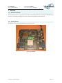
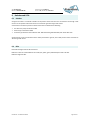
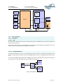
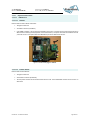
BlueVD4 Board
User Manual
BLUEVD4-BRD-UM
Version 1.01
2010-06-24
RivieraWaves
http://www.rivierawaves.com/
RivieraWaves confidential. This document is copyrighted and released under CDA or NDA only. Do not copy or distribute without written
authorization from RivieraWaves. Please check with RivieraWaves that this document is the latest release.
Title: BlueVD4 Board
Reference: BLUEVD4-BRD-UM
Document type: User Manual
Version: 1.01, Release Date: 2010-06-24
Revision history
Version
Date
Revision description
Author
1.00
2010-04-01
Initial Release
JPL
1.01
2010-06-24
Typos correction in switch explanation table
JPL
Changes between a version and the previous one is reflected by the addition of change bars, like for the line below:
…This line has been modified from previous version…
Confidential – © 2010 RivieraWaves
Page 2 of 41
Title: BlueVD4 Board
Reference: BLUEVD4-BRD-UM
Document type: User Manual
Version: 1.01, Release Date: 2010-06-24
Table of contents
Revision history .......................................................................................................................................................... 2
Table of contents ....................................................................................................................................................... 3
List of Figure ............................................................................................................................................................... 5
List of Table ................................................................................................................................................................ 6
1
Overview ........................................................................................................................................................... 7
1.1
1.2
2
Document overview ............................................................................................................................................. 7
System pictures .................................................................................................................................................... 7
BlueVD4 board quick start ................................................................................................................................. 8
2.1
2.2
3
Power up .............................................................................................................................................................. 8
Programming HW Flash ....................................................................................................................................... 9
ARM7S chip JTAG ............................................................................................................................................. 11
3.1
3.2
3.3
4
Case of external ARM7S ..................................................................................................................................... 11
Case of internal ARM7S...................................................................................................................................... 11
Case of internal and external ARM7S ................................................................................................................ 12
Xilinx JTAG chain .............................................................................................................................................. 13
4.1
4.2
FPGA JTAG chain ................................................................................................................................................ 13
CPLD JTAG Chain ................................................................................................................................................ 13
5
System reset .................................................................................................................................................... 14
6
Switches and LEDs ............................................................................................................................................ 15
6.1
6.2
7
Switches ............................................................................................................................................................. 15
LEDs .................................................................................................................................................................... 15
Daughter boards .............................................................................................................................................. 16
7.1
BlueVD4 application daughter board ................................................................................................................. 16
7.1.1
Features description ..................................................................................................................................... 17
7.1.1.1
HCI Support.............................................................................................................................................................. 17
7.1.1.1.1 FTDI ....................................................................................................................................................................... 17
7.1.1.1.2 Integrated USB Device .......................................................................................................................................... 17
7.1.1.2
Supported radio modules ........................................................................................................................................ 18
7.1.1.2.1 Fallback BT1.2 ....................................................................................................................................................... 18
7.1.1.2.1.1 SiW1701 ......................................................................................................................................................... 18
7.1.1.2.1.2 Semtech XE1413 ............................................................................................................................................. 18
7.1.1.2.1.3 RivieraWaves Bluejay Bluetooth radio ........................................................................................................... 19
7.1.1.3
MMI devices (optional) ............................................................................................................................................ 19
7.1.1.4
Keypad (optional) .................................................................................................................................................... 20
7.1.1.5
Display (optional) ..................................................................................................................................................... 20
7.1.1.6
PCM ......................................................................................................................................................................... 20
7.1.1.7
Configuration capabilities ........................................................................................................................................ 20
7.1.1.8
Power supplies ......................................................................................................................................................... 21
7.1.2
7.1.2.1
7.1.2.2
Digital signals ................................................................................................................................................ 21
Digital signal correspondence table......................................................................................................................... 22
Power correspondence table................................................................................................................................... 23
7.1.3
Part list ......................................................................................................................................................... 24
7.2
BlueVD4 BlueJay TC1 daughter board (optional) ............................................................................................... 24
7.2.1
Overview ...................................................................................................................................................... 24
7.2.1.1
7.2.1.2
RF Device Characterization Board............................................................................................................................ 25
Bluetooth System Application Board ....................................................................................................................... 25
Confidential – © 2010 RivieraWaves
Page 3 of 41
Title: BlueVD4 Board
Reference: BLUEVD4-BRD-UM
7.2.2
Requirements ............................................................................................................................................... 26
7.2.2.1
7.2.2.2
7.2.2.2.1
7.2.2.2.2
7.2.2.3
7.2.2.3.1
7.2.2.3.2
7.2.2.4
7.2.2.5
7.2.3
8
BB Interface ............................................................................................................................................................. 26
Multiple BB Control Sources .................................................................................................................................... 26
Multiple BB Control Sources ................................................................................................................................. 26
Multiple SPI Sources ............................................................................................................................................. 27
Powering Sources .................................................................................................................................................... 28
Characterization ................................................................................................................................................... 28
Application Board ................................................................................................................................................. 28
Spare Area ............................................................................................................................................................... 28
BlueVD4 Requirements ............................................................................................................................................ 28
Digital signals ................................................................................................................................................ 29
7.2.3.1
7.2.3.2
7.2.4
Document type: User Manual
Version: 1.01, Release Date: 2010-06-24
Digital signal corresponding table ........................................................................................................................... 29
VD4BJ1DB Power correspondence table ................................................................................................................. 30
Part list ......................................................................................................................................................... 31
Connector connections .................................................................................................................................... 32
8.1
Digital interface .................................................................................................................................................. 32
8.2
Test Connectors ................................................................................................................................................. 35
8.2.1
FPGA1 ........................................................................................................................................................... 35
8.2.2
FPGA2 ........................................................................................................................................................... 37
9
Problems on board........................................................................................................................................... 40
9.1
9.2
Nothing is running .............................................................................................................................................. 40
FPGA problem .................................................................................................................................................... 40
References ............................................................................................................................................................... 41
Confidential – © 2010 RivieraWaves
Page 4 of 41
Title: BlueVD4 Board
Reference: BLUEVD4-BRD-UM
Document type: User Manual
Version: 1.01, Release Date: 2010-06-24
List of Figure
Figure 1.1 – BlueVD4 board ................................................................................................................................................ 7
Figure 2.1 – BlueVD4 overview .......................................................................................................................................... 8
Figure 2.2 – BlueVD4 board with BLUE POD ...................................................................................................................... 9
Figure 2.3 – FlashProg interface ....................................................................................................................................... 10
Figure 3.1 – External ARM7S JTAG ................................................................................................................................... 11
Figure 3.2 – Internal ARM7S JTAG .................................................................................................................................... 11
Figure 3.3 – Internal and external ARM7S........................................................................................................................ 12
Figure 5.1 – System reset ................................................................................................................................................. 14
Figure 7.1 – Future daughter board ................................................................................................................................. 16
Figure 7.2 – BlueVD4 Bluetooth System ........................................................................................................................... 17
Figure 7.3 – USB configuration ......................................................................................................................................... 17
Figure 7.4 – Siw RF module plugged on VD4BTDB ........................................................................................................... 18
Figure 7.5 – Xemics/Semtech RF module plugged on VD4BTDB ...................................................................................... 19
Figure 7.6 – Keypad and display mounted for full embedded applications ..................................................................... 19
Figure 7.7 – BlueJay TC1 RF board mounted on VD4 mother board ................................................................................ 25
Figure 7.8 – VD4 Bluetooth System .................................................................................................................................. 25
Figure 7.9 – BlueVD4 Bluetooth System ........................................................................................................................... 26
Figure 7.10 – Aardvark Connector Description ................................................................................................................ 27
Confidential – © 2010 RivieraWaves
Page 5 of 41
Title: BlueVD4 Board
Reference: BLUEVD4-BRD-UM
Document type: User Manual
Version: 1.01, Release Date: 2010-06-24
List of Table
Table 7.1 – Configuration switches .................................................................................................................................. 21
Table 7.2 – Digital signal list ............................................................................................................................................. 21
Table 7.3 – Digital pin correspondence between BlueVD4 and VD4BTDB ....................................................................... 23
Table 7.4 – Digital power correspondence between BlueVD4 and VD4BTDB ................................................................. 24
Table 7.5 – VD4BTDB Part list........................................................................................................................................... 24
Table 7.6 – Bluejay TC1 Baseband Interface .................................................................................................................... 26
Table 7.7 – Bluejay TC1 Power Lines ................................................................................................................................ 28
Table 7.8 – BlueVD4 Requirements .................................................................................................................................. 29
Table 7.9 – Digital signal list ............................................................................................................................................. 29
Table 7.10 – Digital pin relation between BlueVD4 and VD4BJ1DB ................................................................................. 30
Table 7.11 – Digital power correspondence between BlueVD4 and VD4BJ1DB .............................................................. 30
Table 7.12 – VD4BJ1DB Part list ....................................................................................................................................... 31
Table 8.1 – Digital Port connections ................................................................................................................................. 35
Table 8.2 – FPGA1 test connectors................................................................................................................................... 37
Table 8.3 – FPGA2 test connectors................................................................................................................................... 39
Confidential – © 2010 RivieraWaves
Page 6 of 41
Title: BlueVD4 Board
Reference: BLUEVD4-BRD-UM
1
1.1
Document type: User Manual
Version: 1.01, Release Date: 2010-06-24
Overview
Document overview
This document describes the connections and set up for the BlueVD4 board kit, consisting of a BlueVD4 board, a
transformer, an application daughter board, and an optional RF daughter board for BlueJay TC1.
1.2
System pictures
The following picture shows the BlueVD4 board in standalone mode.
Figure 1.1 – BlueVD4 board
Confidential – © 2010 RivieraWaves
Page 7 of 41
Title: BlueVD4 Board
Reference: BLUEVD4-BRD-UM
2
Document type: User Manual
Version: 1.01, Release Date: 2010-06-24
BlueVD4 board quick start
On the following board diagram, the useful connectors and switches are highlighted in order to quickly find them on
the actual board. The necessary connections are detailed below.
FPGA2 1V8
daughter board
FPGA2 3V3
daughter board
3V3 @ 5A
transformer
Powe r LEDs
FPGA1 3V3
daughter board
POWER
ARM7S
FPGA1 1V8
daughter board
FPGA 2
FPGA2
clock test
osc
osc
FPGA2
LEDs
osc
SRAM
Push
Button
rese t
FLASH
FPGA1
clock test
SRAM
EEPROM
Configuration
switch
FPGA2 test
osc
FPGA
configuration
FPGA 1
CPLD
FPGA1 test
CONFIG
connector
HW
FLASH
Eagle
(RF)
JTAG
connector
ARM
MultiIce
UART
Soft use d
LEDs
FPGA1
LEDs
ETM7
connector
Digital
inte rface
connectors
FPGA1 switch
Figure 2.1 – BlueVD4 overview
2.1
Power up
The power up of the BlueVD4 board is very simple. Power the board with the correct transformer: 3V3 @ 5A to supply
the board.
Transformer part reference: SB-035A0F-11, 3V3 @ 5A from Stontronics
Jack connector + inside, - outside
IMPORTANT: Never connect a transformer with higher voltage than 3V3 to supply the BlueVD4 board, it will be
severely damaged.
Once the board is powered, the FPGA is loaded with the binary stored in the HW Flash. At the end of loading, the
orange LED “FPGA configuration” becomes on and indicates that the FPGA is correctly configured and ready to start.
If the LED “FPGA configuration” is not ON at the power up of the board, please refer to chapter 9.2.
Confidential – © 2010 RivieraWaves
Page 8 of 41
Title: BlueVD4 Board
Reference: BLUEVD4-BRD-UM
2.2
Document type: User Manual
Version: 1.01, Release Date: 2010-06-24
Programming HW Flash
The necessary tools to program the HW Flash on the board are:
BLUE POD: Small RivieraWaves HW box used to connect a PC to the board.
FlashProg: RivieraWaves Software program running on the PC, minimum version 4.6.
The following list details how to connect the Blue POD to the BlueVD4 board:
Check in the BIOS of your computer that the parallel port is set in EPP mode before launching Windows™.
Connect the BLUE POD to the serial link connector called CONFIG connector (J7) on Figure 2.1.
Connect the other side of the BLUE POD to the parallel port of the PC. Please check that no other application is
using the parallel port at the same time.
Place switch 4 of INT1 to ON. INT1 switch is called configuration switch on Figure 2.1.
Figure 2.2 – BlueVD4 board with BLUE POD
The final step to program the HW Flash is to launch the FlashProg software:
Power up the board with the correct supply.
Launch FlashProg on the connected PC. Minimum version of FlashProg must be 4.6.
Select the FPGA1 tick box (please refer to 1 on Figure 2.3).
Select the correct Platform: WiLDSYSFPGA, see 2 on Figure 2.3.
Going through “…”, select the corresponding HW binary (.bit file*) for FPGA1. Refer to 3 on Figure 2.3. FPGA2
field is useless for the BlueVD4 platform, as FPGA2 is not mounted.
Click on the program button.
At the end of the programming, the orange LED (“FPGA configuration”) must be on, indicating that the FPGA is
programmed with the new file stored inside the HW Flash.
* Don’t forget the necessary option in Xilinx ISE to generate the .bit file : Startup options FPGA Start Up Clock CCLK
Confidential – © 2010 RivieraWaves
Page 9 of 41
Title: BlueVD4 Board
Reference: BLUEVD4-BRD-UM
Document type: User Manual
Version: 1.01, Release Date: 2010-06-24
3. Select the
corresponding .bit
file program
1. Select which one or
both FPGA to program
Riviera
Waves
2. Select the
correct platform
Figure 2.3 – FlashProg interface
Confidential – © 2010 RivieraWaves
Page 10 of 41
Title: BlueVD4 Board
Reference: BLUEVD4-BRD-UM
3
Document type: User Manual
Version: 1.01, Release Date: 2010-06-24
ARM7S chip JTAG
The BlueVD4 features an ARM7TDMI processor, directly mounted on the board (external ARM7TDMI). The user can
also synthesize its own ARM7S processor and can integrate it directly in the FPGA (internal ARM7S).
Whatever the type of processor used, being internal or external, the processor JTAG is accessible through a “MultiIce”
connector, see Figure 2.1. This JTAG chain provides a serial line to the processor, and eases the real time debugging.
3.1
Case of external ARM7S
To use the external ARM7S JTAG chip, connect the ARMS_CHIP_TDO FPGA input to the ARMS_TDO FPGA output.
ARMS_TCK
ARMS
MultiIce
ARMS_TMS
ARMS_nTRST
ARMS_TDI
ARMS_TDO
ARMS_CHIP_TDO
FPGA1
ARM7TDMIS
Test Chip
Figure 3.1 – External ARM7S JTAG
3.2
Case of internal ARM7S
In case of internal ARM7S use only, just connect the JTAG lines to the ARM7S block, leave unconnected the
ARMS_CHIP_TDO from the external ARM7S.
ARMS_TCK
ARMS
MultiIce
ARMS_TMS
ARMS_nTRST
ARMS_TDI
ARMS_TDO
ARM7S
ARMS_CHIP_TDO
FPGA1
ARM7TDMIS
Test Chip
Figure 3.2 – Internal ARM7S JTAG
Confidential – © 2010 RivieraWaves
Page 11 of 41
Title: BlueVD4 Board
Reference: BLUEVD4-BRD-UM
3.3
Document type: User Manual
Version: 1.01, Release Date: 2010-06-24
Case of internal and external ARM7S
In that case, connect the JTAG data of the both ARM7S in serial mode as shown below.
ARMS_TCK
ARMS
MultiIce
ARMS_TMS
ARMS_nTRST
ARMS_TDI
ARMS_TDO
TDO
ARM7S
TDI
ARMS_CHIP_TDO
FPGA1
ARM7TDMIS
Test Chip
Figure 3.3 – Internal and external ARM7S
Confidential – © 2010 RivieraWaves
Page 12 of 41
Title: BlueVD4 Board
Reference: BLUEVD4-BRD-UM
4
4.1
Document type: User Manual
Version: 1.01, Release Date: 2010-06-24
Xilinx JTAG chain
FPGA JTAG chain
The Xilinx JTAG chain can be used for programming the binary and provides also read back capabilities, if used with
the correct ISE tool from Xilinx.
To see the FPGA JTAG chain, connect your parallel PC cable and Xilinx box to the JTAG connector (J18) on board, see
Figure 2.1.
There is a FGPA JTAG chain only for the FPGA1 or both for FPGA1 and FPGA2. By default, the FPGA JTAG chain of the
board is configured only for FPGA1: R80 mounted and R81 not mounted. To connect FPGA2 to the XILINX JTAG chain,
just reverse the two resistors: R80 not mounted and R81 mounted. R81 and R80 are zero Ohm resistors.
Important: FPGA2 is not mounted on the BlueVD4 prototyping board.
With IMPACT software from Xilinx, it is possible to load the FPGAs directly with their programs, without using the
CPLD and the HW Flash. Note that the .bit file must be generated with the necessary option in Xilinx ISE: Startup
options FPGA Start Up Clock JTAG.
The main disadvantage of this kind of FPGA loading is that programs are lost once the power is removed, and it is
necessary to reload the program inside the FPGA with IMPACT software at each power up. Note that the JTAG
programming is very slow compared to programming through the CPLD.
4.2
CPLD JTAG Chain
The CPLD JTAG chain is separate from the FPGA JTAG chain due to different supply voltages (3V3 for CPLD and 2V5 for
FPGA). Access to the CPLD is done via IMPACT software from XILINX. The same connector is used for both the HW
Flash loading and CPLD configuration, i.e CONFIG connector (J7), see Figure 2.1. To switch to the CPLD chain instead of
HW Flash loading chain, put switch 4 of INT1 OFF (INT1 switch is called configuration switch on Figure 2.1).
The CPLD is already loaded with the RivieraWaves program and has the following features:
Automatically loads program(s) from the HW Flash to the FPGA(s) at power up.
Transfers the FPGA programs from the PC into the HW Flash component.
Handles system reset of the board. For more information about system reset, see chapter 5.
PCMCIA configuration start, when digital interface is used as PCMCIA (CVS and CCD signals).
Confidential – © 2010 RivieraWaves
Page 13 of 41
Title: BlueVD4 Board
Reference: BLUEVD4-BRD-UM
5
Document type: User Manual
Version: 1.01, Release Date: 2010-06-24
System reset
The CPLD handles the system reset of the BlueVD4 board.
The different reset sources are going to the CPLD, and the CPLD transmits them to the main components on board.
Reset sources:
Voltage supervisor reset.
End of FPGA configuration signal.
Push Button Reset.
PCMCIA reset coming from Digital interface (if Digital interface is used as PCMCIA).
Reset coming from the RF (Eagle) interface.
Component resets handled by CPLD:
FPGA1
FPGA2
HW_Flash
Radio board
For the radio board, the choice is offered between a reset coming directly from CPLD (load R103 and remove R104) or
a resent passing through FPGA (load R104 and remove R103).
Voltage
Supervisor
Push
Button
Reset
PCMCIA
Reset
HW Flash
HWF_nRST
RF_RST
FPGA1_nRST
FPGA2_nRST
RF Eagle
Board
CPLD
FPGA 2
RF_RST
MultiIce
nTRST
ARM
Processor
SW Flash
FPGA 1
Config_done
Config_done
nRST
SWF_nRST
Figure 5.1 – System reset
Confidential – © 2010 RivieraWaves
Page 14 of 41
Title: BlueVD4 Board
Reference: BLUEVD4-BRD-UM
6
6.1
Document type: User Manual
Version: 1.01, Release Date: 2010-06-24
Switches and LEDs
Switches
An eight lines switch is connected to FPGA1. An ON position means that the line is connected to 3V3 through a 10K
resistor. An OFF position means that the line is connected to ground through a 10K resistor.
A second four line switch is present on board and the lines are distributed as following:
First two lines (1 & 2) connected to CPLD
Third line (3) connected to FPGA2
Fourth line (4) allows the choice between: ON: HW Flash loading with BLUE POD, OFF: CPLD JTAG chain.
An ON position on the second switch means directly connected to ground, and an OFF position means connected to
3V3 through 10K resistor.
6.2
LEDs
Each FPGA has eight external LED connections.
FPGA1 has a first set of three different color LEDs (red, yellow, green) followed by five others red LEDs.
FPGA2 has eight red LEDs.
Confidential – © 2010 RivieraWaves
Page 15 of 41
Title: BlueVD4 Board
Reference: BLUEVD4-BRD-UM
7
Document type: User Manual
Version: 1.01, Release Date: 2010-06-24
Daughter boards
For future daughter boards, there are five available connectors on the BlueVD4 board.
Two are connected to FPGA1.
Three are connected to FPGA2.
Both small connectors (64 pins) are each connected to an entire bank of each FPGA. That is to say that all the signals
of the bank and consequently of the connector can have the same voltage standard which is on board configurable.
Four holes are available on the BlueVD4 board to attach the daughter board.
POWER
ARM7S
osc
osc
SRAM
SRAM
FPGA 1
osc
osc
FLASH
FPGA 2
EEPROM
CPLD
HW
FLASH
Figure 7.1 – Future daughter board
7.1
BlueVD4 application daughter board
This section describes the daughter board that enables the BlueVD4 development board, to add complete Bluetooth
functionality. The code name of this board is VD4BTDB. Figure 7.2 depicts the envisioned system:
Confidential – © 2010 RivieraWaves
Page 16 of 41
Title: BlueVD4 Board
Reference: BLUEVD4-BRD-UM
Document type: User Manual
Version: 1.01, Release Date: 2010-06-24
BlueVD4
SIW1701 /
SKY72313
FPGA2
USB
UART
VD4BTDB
KEYPAD
FPGA1
VD4BJ1DB
DISPLAY
A7
PCM
Power
Power
Figure 7.2 – BlueVD4 Bluetooth System
7.1.1
7.1.1.1
7.1.1.1.1
Features description
HCI Support
FTDI
An external FIFO-to-USB chip will be used to convey the Bluetooth HCI. FT245BM Chip [2] from FTDI plus USB Series B
connector female are used.
Integrating the USB chip directly on the VD4BTDB, has the advantage to avoid adding another daughter board. In this
case, just an external crystal and passive components are needed.
7.1.1.1.2
Integrated USB Device
To support the configuration in which a standard USB Device controller would be instantiated within BlueVD4, an USB
Series B connector female and Philips Transceiver: PDIUSBP11ADB are needed in the VD4BTDB. USB standard version
is 1.1.
In case of the FT245BM being integrated in the VD4BTDB, the interface to the USB connector should be routed either
from the FTDI port or from the Philips transceiver (configurable, see Table 7.1).
Philips
Transceiver
USB
Connector
D+ & D- USB lines
FTDI
Transceiver
Figure 7.3 – USB configuration
Confidential – © 2010 RivieraWaves
Page 17 of 41
Title: BlueVD4 Board
Reference: BLUEVD4-BRD-UM
7.1.1.2
Document type: User Manual
Version: 1.01, Release Date: 2010-06-24
Supported radio modules
7.1.1.2.1
Fallback BT1.2
7.1.1.2.1.1
SiW1701
Interface with the Silicon Wave radio board:
•
13 digital control lines
•
2x12 Male connector (kind HE14)
•
A 32.768KHz oscillator is to be mounted on BlueVD4. The goal is to replace the low power clock from Silicon
Wave board not always present (depends on the board version). Low power clock selection between internal
/ external source is to be performed inside BlueVD4 as per Silicon Wave board version.
Figure 7.4 – Siw RF module plugged on VD4BTDB
7.1.1.2.1.2
Semtech XE1413
Interface with Semtech XE1413
•
11 digital control lines
•
2x15 Female connector (kind HE14)
•
The low power oscillator of the Semtech radio board is used. The local BlueVD4 oscillator can be used as an
alternative.
Confidential – © 2010 RivieraWaves
Page 18 of 41
Title: BlueVD4 Board
Reference: BLUEVD4-BRD-UM
Document type: User Manual
Version: 1.01, Release Date: 2010-06-24
Figure 7.5 – Xemics/Semtech RF module plugged on VD4BTDB
7.1.1.2.1.3
RivieraWaves Bluejay Bluetooth radio
To be connected to BlueVD4 through a dedicated daughter board. This requirement falls outside the scope of
VD4BTDB, but is captured here for reference purposes. The interface with the Bluejay TC1 radio board is as follows:
•
14 digital control lines
•
Male/connector (MOLC_120_02_S_Q_LC, 80 pin)
•
The 32.768KHz clock is taken from the oscillator to be mounted on BlueVD4.
7.1.1.3
MMI devices (optional)
Keypad and LCD could be either:
•
Mounted via a ribbon cable as side components
•
Screwed over the VD4BTDB
Figure 7.6 – Keypad and display mounted for full embedded applications
Confidential – © 2010 RivieraWaves
Page 19 of 41
Title: BlueVD4 Board
Reference: BLUEVD4-BRD-UM
7.1.1.4
Document type: User Manual
Version: 1.01, Release Date: 2010-06-24
Keypad (optional)
Interface with Keypad is a simple 8x1 connector. The 8x1 connector is defined to drive:
•
4 vertical lines
•
4 horizontal lines
Keypad features:
•
Matrixed
•
16 buttons
7.1.1.5
Display (optional)
As for the keypad, there is a display connector on the VD4BTDB to connect a display.
The display is already a mini board with a complete digital interface:
•
11 lines (8 data bits plus 3 control lines Select, read, write).
Should the option of mounting the LCD above VD4BTDB be retained, the potentiometer used to tune it shall not be
covered, allowing easy access to the rotating wiper.
7.1.1.6
PCM
A PCM interface is available on the BCARDDB with a PCM codec and Jack connectors. This interface allows a user to
connect a headset.
PCM Codec: MC145483 from Motorola
Audio jacks: two 3.5mm 3 PTS audio jacks (green for speaker, pink for microphone, PC color convention)
To ensure structural solidity, the audio jacks need to be mounted through the PCB, not just surface soldered.
7.1.1.7
Configuration capabilities
The configuration switch INT1 allows:
•
Selecting the radio interface,
•
Selecting the way of connecting to the host system, UART or FTDI,
•
Selecting how is routed the PCM output from the FPGA,
•
Selecting the source of the main reset.
The Table 7.1 describes the configurations available.
Confidential – © 2010 RivieraWaves
Page 20 of 41
Title: BlueVD4 Board
Reference: BLUEVD4-BRD-UM
Switch
1
2
3, 4, 5
6
Document type: User Manual
Version: 1.01, Release Date: 2010-06-24
Value
On
Off
On
Off
On-On-On
Off-On-On
On-Off-On
On
Off
Action
Select UART to support HCI
Select FTDI to support HCI, this is the default value
Select PCM routed to audio codec
Select PCM routed to dedicated connector, this is the
default value
RADIO_CONF: Select the connected RF chip.
On-On-On: SiW // Off-On-On: XE1314 // On-Off-On: BJ
TC1
Reset coming from on board reset button
Reset coming from BlueJay RF reset button, this is the
default value when BlueJay RF module is used
Table 7.1 – Configuration switches
Important: Switch to On means logical value ‘0’, whereas switch to Off means logical value ‘1’.
7.1.1.8
Power supplies
The 3V3 voltage present on the BlueVD4 is passed to the VD4BTDB through the daughter board connectors. One pin
per connector is dedicated to 3V3 voltage.
The 5V needed by the FT245BM USB chip is coming directly from the USB interface (i.e. from the PC).
The 5V needed by the display, is done with a Linear step-up regulator: LT1930ES5 from the 3V3 analog present on
board.
Power sources available in BlueVD4 are listed in section 7.1.2.2.
7.1.2
Digital signals
The following table lists all the digital signals coming from BlueVD4. It also explains how these signals are mapped on
the connector interface between BlueVD4 and VD4BTDB.
USB Philips Transceiver
Number of signal
from FPGA
8
RCV, OE, SUSPEND, VM, VP, VMO, VPO, SPEED
USB FTDI
14
D[7,0], RD#, WR, TXE#, RXF#, PWREN#, RESET#
Digital Interface
Signal list
KEYPAD
8
V[3,0], H[3,0]
DISPLAY
11
DB[7,0], E, RS, RW
SKY72313/XE1413/BTRF
2
SYS_CLK_OUT/BB_CLK, SYNC_FOUND/ENABLE_RM
SPI Bus for fallback 1.2 Radio
4
SPI_SMD, SPI_MSD, SPI_SS_N, SPI_CLK
Control Bus for fallback 1.2 Radio
6
PCM_Bus
Switch
4
6
CD_TXEN, RX_TX_DATA, TX_DATA_UNI, BB_32K,
HOP_STRB, RM_RESET
PCM_DOUT, PCM_CLK, PCM_DIN, PCM_FSYNC
2 for radio selection, 4 free.
Diagnostic
TOTAL
8
71
8 output ports for logic analyzer
Table 7.2 – Digital signal list
Confidential – © 2010 RivieraWaves
Page 21 of 41
Title: BlueVD4 Board
Reference: BLUEVD4-BRD-UM
7.1.2.1
Document type: User Manual
Version: 1.01, Release Date: 2010-06-24
Digital signal correspondence table
The following table explains the relation between VD4BTDB and BlueVD4 signals, stating the correspondence
between signal names in the schematics, connector pins and FPGA pins. The connector J3 is used to plug VD4BTDB on
top of the BlueVD4 motherboard. The corresponding bus in the BlueVD4 schematic is FPGA1_DGHT.
BlueVD4
FPGA1
VD4BTDB Digital Interface VD4BTDB Signal name VD4BTDB Connector
FPGA1_DGHT(i)
Pin
connector Pin
Connector Pin
PDIU_RCV
11
J1-A12
J3-A12
U17-L/D1
PDIU_OE
12
J1-A13
J3-A13
U17-L/E4
PDIU_SUSPEND
38
J1-B14
J3-B14
U17-L/K7
PDIU_VM
13
J1-A14
J3-A14
U17-L/E3
PDIU_USB_BUS : USB Philips
PDIU_VP
14
Transceiver
J1-A15
J3-A15
U17-L/F2
PDIU_VMO
15
J1-A16
J3-A16
U17-L/F1
PDIU_VPO
16
J1-A17
J3-A17
U17-L/F6
PDIU_SPEED
17
J1-A18
J3-A18
U17-L/F5
FTDI_D7
J1-C15
J3-C15
64
U17-P/N4
FTDI_D6
65
J1-C16
J3-C16
U17-P/N3
FTDI_D5
91
J1-D17
J3-D17
U17-P/T9
FTDI_D4
66
J1-C17
J3-C17
U17-P/N2
FTDI_D3
92
J1-D18
J3-D18
U17-P/T8
FTDI_D2
93
J1-D19
J3-D19
U17-P/T6
FTDI_D1
94
J1-D20
J3-D20
U17-P/T5
FTDI_USB_BUS : USB FTDI
FTDI_D0
95
J1-D21
J3-D21
U17-P/T4
Transceiver
FTDI_nRXF
96
J1-D22
J3-D22
U17-P/T3
FTDI_nTXE
71
J1-C22
J3-C22
U17-P/P6
FTDI_nRD
97
J1-D23
J3-D23
U17-P/T1
FTDI_WR
72
J1-C23
J3-C23
U17-P/P5
KEYPAD_BUS : Bus for
external Keypad
LCD_BUS : Bus for external
Display
RADIO_BT1.2
RF_BT1.2_SPI_BUS
Confidential – © 2010 RivieraWaves
FTDI_nRESET
J1-C24
J3-C24
73
U17-P/P4
FTDI_nPWREN
J1-C25
J1-A6
J1-A7
J1-B8
J1-A8
J1-A9
J1-B10
J1-A10
J1-A11
J1-C1
J1-D2
J1-C2
J1-D3
J1-C3
J1-D4
J1-C4
J1-D5
J1-C5
J1-D6
J1-D7
J1-B5
J1-B6
J1-B1
J1-B2
J3-C25
J3-A6
J3-A7
J3-B8
J3-A8
J3-A9
J3-B10
J3-A10
J3-A11
J3-C1
J3-D2
J3-C2
J3-D3
J3-C3
J3-D4
J3-C4
J3-D5
J3-C5
J3-D6
J3-D7
J3-B5
J3-B6
J3-B1
J3-B2
74
U17-P/P2
U17-L/B3
U17-L/C4
U17-L/I7
U17-L/C3
U17-L/C2
U17-L/I5
U17-L/D4
U17-L/D2
U17-L/M11
U17-L/R16
U17-L/M10
U17-L/R14
U17-L/M8
U17-L/R12
U17-L/M7
U17-L/R11
U17-L/M6
U17-L/R9
U17-L/R8
U17-P/H4
U17-P/H3
U17-L/G2
U17-L/G1
KEY_V3
KEY_V2
KEY_V1
KEY_V0
KEY_H3
KEY_H2
KEY_H1
KEY_H0
LCD_DB7
LCD_DB6
LCD_DB5
LCD_DB4
LCD_DB3
LCD_DB2
LCD_DB1
LCD_DB0
LCD_E
LCD_RW
LCD_RS
BB_CLK(1)
ENABLE_RM(2)
SPI_SS_N
SPI_CLK
5
6
32
7
8
34
9
10
50
76
51
77
52
78
53
79
54
80
81
29
30
25
26
Page 22 of 41
Title: BlueVD4 Board
Reference: BLUEVD4-BRD-UM
Document type: User Manual
Version: 1.01, Release Date: 2010-06-24
SPI_MSD
SPI_SMD
RM_RESET
HOP_STRB
TX_DATA_UNI
CD_TXEN
RX_TX_DATA
BB_32K
PCM_CLK
PCM_FSYNC
PCM_DIN
PCM_DOUT
SWITCH1
SWITCH2
SWITCH3
SWITCH4
SWITCH5
SWITCH6
DIAG0
DIAG1
DIAG2
DIAG3
DIAG4
DIAG5
DIAG6
DIAG7
71
RF_BT1.2_CTRL_BUS
PCM_BUS : Digital PCM
interface
SWITCH6_1 : Switches for
control
DIAG7_0 : Switches for
control
TOTAL
J1-B3
J1-B4
J1-C11
J1-C12
J1-D13
J1-C13
J1-D14
J1-D15
J1-A19
J1-B20
J1-A20
J1-B21
J1-C7
J1-D8
J1-C8
J1-D9
J1-C9
J1-D10
J1-A21
J1-B22
J1-A22
J1-B23
J1-A23
J1-B24
J1-A24
J1-B25
J3-B3
J3-B4
J3-C11
J3-C12
J3-D13
J3-C13
J3-D14
J3-D15
J3-A19
J3-B20
J3-A20
J3-B21
J3-C7
J3-D8
J3-C8
J3-D9
J3-C9
J3-D10
J3-A21
J3-B22
J3-A22
J3-B23
J3-A23
J3-B24
J3-A24
J3-B25
27
28
60
61
87
62
88
89
18
44
19
45
56
82
57
83
58
84
20
46
21
47
22
48
23
49
U17-L/H7
U17-L/H5
U17-L/N10
U17-L/N8
U17-L/T15
U17-L/N7
U17-L/T14
U17-L/T13
U17-L/F4
U17-L/L8
U17-L/F3
U17-L/L6
U17-P/M3
U17-P/R6
U17-P/M2
U17-P/R4
U17-P/M1
U17-P/R3
U17-P/Y13
U17-P/L5
U17-P/Y11
U17-P/L4
U17-P/Y9
U17-P/L3
U17-P/AA11
U17-P/L1
Table 7.3 – Digital pin correspondence between BlueVD4 and VD4BTDB
Notes:
(1) This signal carries the clock from the RF device to the baseband (it is an input to BlueVD4’s FPGA1). Note that
this clock may or may not be actually used to clock the entire system: this decision is made inside BlueVD4’s
FPGA1. The signal names are:
a.
BB_CLK (SiW)
b.
CNX_SYS_CLK_OUT (Semtech)
(2) This signal carries different information depending on the destination RF device. This signal is an output of
BlueVD4’s FPGA1, where the selection of the actual signal source is carried out:
7.1.2.2
a.
ENABLE_RM (SiW) : RF Power down indication from baseband
b.
SYNC_DET (Semtech): Baseband signal telling RF device that packet synchronization has been
achieved.
Power correspondence table
Table 7.4 shows the power supply signals available in BlueVD4’s J3 connector:
Confidential – © 2010 RivieraWaves
Page 23 of 41
Title: BlueVD4 Board
Reference: BLUEVD4-BRD-UM
Document type: User Manual
Version: 1.01, Release Date: 2010-06-24
VD4BTDB Digital Interface
BlueVD4
Signal name
Vcc_3.3V
Power
J3-D27
Vcc_3.3V
J3-A1
GND
J3-A2
GND
J3-A3
GND
J3-B26
GND
J3-A26
GND
J3-A27
GND
Ground
J3-D26
GND
J3-C26
GND
J3-C27
GND
J3-C28
GND
J3-C29
GND
J3-C30
GND
TOTAL
BlueVD4
connector Pin
J3-B27
13
Table 7.4 – Digital power correspondence between BlueVD4 and VD4BTDB
7.1.3
Part list
The following table summarizes the components used in the VD4BTDB:
Part Number
LT1930ES5
FT245BM
MC145483DW
ROLC_130_02_S_Q_LC
ANTELEC BAR 15x2
HE14 12x2
FCN_724P016_AU/W
HE14 8x1
TOBY STX_3150_5N_577C
TOBY STX_3150_5N_701C
PDIUSBP11ADB
MOLEX_CON_USB_TYPE_B
FCN_724P016_AU/W
IKN0604000
RivieraWaves Stock
Y
BeTech
Y
Y
BeTech
BeTech
BeTech
BeTech
Y
Y
Y
BeTech
BeTech
BeTech
Description
Step-up regulator for LCD
FTDI UART 2 USB I/F Chip
Audio codec
Male connector 120 pin
Semtech board connector
SiW board connector
LCD Connector
KP Connector
Audio jack 3.5mm (Microphone)
Audio jack 3.5mm (Speaker)
Philips USB 1.1 PHY transceiver
USB-TYPE-B connector
Logic Analyzer connector
Switches
Table 7.5 – VD4BTDB Part list
7.2
7.2.1
BlueVD4 BlueJay TC1 daughter board (optional)
Overview
This section describes the Daughter Board that enables
Confidential – © 2010 RivieraWaves
Page 24 of 41
Title: BlueVD4 Board
Reference: BLUEVD4-BRD-UM
Document type: User Manual
Version: 1.01, Release Date: 2010-06-24
•
The characterization of the Bluejay TC1 device
•
The BLUEVD4 development board adds Bluetooth RF link functionality by using Blue jay TC1.
The code name of this board is VD4BJ1DB. The two different roles played by this board are outlined below.
The Figure 7.7 shows such a daughter board connected to the BlueVD4 board, on the right side of the picture.
Figure 7.7 – BlueJay TC1 RF board mounted on VD4 mother board
7.2.1.1
RF Device Characterization Board
Figure 7.8 depicts the usage of VD4BJ1DB as an RF Characterization vehicle. The board can be connected to external
elements used to perform the characterization process (control and data capture interfaces). This interface to these
elements will be described in section 7.2.2.
VD4BJ1DB
Aardvark
I/Q Capture
Board
Power
Figure 7.8 – VD4 Bluetooth System
7.2.1.2
Bluetooth System Application Board
Figure 7.2 depicts the complete Bluetooth system that uses VD4BJ1DB as RF link. In this case, VD4BJ1DB is connected
to the BlueVD4 motherboard, which is completed with the VD4BTDB (see 7.1) to supply the basic peripherals of a
Bluetooth system.
Confidential – © 2010 RivieraWaves
Page 25 of 41
Title: BlueVD4 Board
Reference: BLUEVD4-BRD-UM
Document type: User Manual
Version: 1.01, Release Date: 2010-06-24
BlueVD4
SIW1701 /
SKY72313
FPGA2
USB
UART
VD4BTDB
KEYPAD
FPGA1
VD4BJ1DB
DISPLAY
A7
PCM
Power
Power
Figure 7.9 – BlueVD4 Bluetooth System
7.2.2
7.2.2.1
Requirements
BB Interface
VD4BJ1DB shall present an interface to the baseband section of the system as described in Table 7.6 below:
Signal Group
SPI I/F
Data I/F
Power
Other Control
System Clock
Pins
4
4
2
3
1
Description
SCLK, MISO, MOSI, N_SS
DATAIO[2:0], DATAIO_VAL
VDD3V3, GND
N_RST, ENABLE_RM, GAIN_SET_STS
BB_CLK
Table 7.6 – Bluejay TC1 Baseband Interface
The baseband interface shall be routed to a 80-pin MOLC_120_02_S_Q_LC male connector (see routing details in
section 7.2.3.1), which will be plugged into connector J20 of the VD4 motherboard. All the signals shall be routed to
Bluejay TC1 in at least one operating mode, as described in section 7.2.2.2.
In order to ease logic analyzer captures of the baseband interface, all the signals in Table 7.6 will be routed to a 16 pin
debug connector.
7.2.2.2
7.2.2.2.1
Multiple BB Control Sources
Multiple BB Control Sources
A provision for an alternative routing to the BlueVD4 interface shall be provided for the following signals:
•
ENABLE_RM
•
N_RST
•
SET_GAIN_STS
A control switch shall be provided in order to route both options accordingly.
Confidential – © 2010 RivieraWaves
Page 26 of 41
Title: BlueVD4 Board
Reference: BLUEVD4-BRD-UM
7.2.2.2.2
Document type: User Manual
Version: 1.01, Release Date: 2010-06-24
Multiple SPI Sources
The SPI interface of Bluejay TC1 shall be driven by either of the interfaces below. A control switch shall be provided in
order to route both options accordingly:
•
The baseband interface (see section 7.2.2.1)
•
The Aardvark bus (see Figure 7.10,and reference [3])
Figure 7.10 – Aardvark Connector Description
Confidential – © 2010 RivieraWaves
Page 27 of 41
Title: BlueVD4 Board
Reference: BLUEVD4-BRD-UM
7.2.2.3
Document type: User Manual
Version: 1.01, Release Date: 2010-06-24
Powering Sources
The powering of VD4BJ1DB takes place in two different modes.
7.2.2.3.1
Characterization
The following supply lines of Bluejay TC1 shall be made available independently, to provide power consumption test
points:
TC1 Pin
2
4
12
28
29
31
32
34
37
38
39
40
Symbol
AVDD_IN_PA
AVDD_RXTX
VDD_3V3
VDD_IN_DIG
VDD_DIG
AVDD_IN_REG
AVDD_ADDA
AVDD_XO
AVDD_XX
AVDD_PLL
AVDD_VCO
VREF_RFPLL
Function
TX driver voltage supply - input
RX/TX block voltage supply – decoupling output
3.3 V supply (for RF_SW)
Digital block voltage supply - input
Digital block voltage supply – decoupling output
Analog block voltage supply 2 - input
RX ADC/TX DAC voltage supply – decoupling output
XO block voltage supply – decoupling output
(Optional pin ## TBD)
PLL block voltage supply – decoupling output
VCO block voltage supply – decoupling output
RFPLL reference decoupling
Table 7.7 – Bluejay TC1 Power Lines
Group the power per voltage levels
Then, decide how to obtain 1.5, 1.2 from 3v3 (and/or 2v5, and/or 1v8, also available in BlueVD4)
Then decide what method will be used to change.
-
from single source
-
to multiple source (grouped)
-
to multiple source (pin by pin)
7.2.2.3.2
Application Board
All the power lines described in section 7.2.2.3.1 need to be supplied in this mode as a single interface connected to
the power section of the baseband connector described in sections 7.2.2.1/7.2.3.1.
7.2.2.4
Spare Area
No spare area for mounting extra components is provided.
7.2.2.5
BlueVD4 Requirements
The requirements specific to BlueVD4 are detailed in Table 7.8 below:
Confidential – © 2010 RivieraWaves
Page 28 of 41
Title: BlueVD4 Board
Reference: BLUEVD4-BRD-UM
Document type: User Manual
Version: 1.01, Release Date: 2010-06-24
Item
Connection to BlueVD4
Description
VD4BJ1DB can be connected to either J20 (FPGA1) or J22 (FPGA2).
Table 7.8 – BlueVD4 Requirements
7.2.3
Digital signals
The following table lists all the digital signals coming from BlueVD4. It also explains how these signals are mapped on
the connector interface between BlueVD4 and VD4BJ1DB.
Number of signal
Signal list
from BlueVD4
15
N_RST, ENABLE_RM, BB_CLK, SCLK, MISO, MOSI, N_SS,
DATAIO[3:0], GAIN_SET_STS, NRST_OUT, IO1, IO0
8
SP_CTRL[7:0]
Digital Interface
Bluejay TC1
`Spare Control Lines
TOTAL
23
Table 7.9 – Digital signal list
7.2.3.1
Digital signal corresponding table
The following table explains the relation between VD4BJ1DB and BlueVD4 signals, stating the correspondence
between signal names in the schematics, connector pins and FPGA pins. The connector J20 is used to plug VD4BJ1DB
on top of the BlueVD4 motherboard. The corresponding bus in the BlueVD4 schematic is FPGA1_1V8_DGHT.
VD4BJ1DB Digital Interface
VD4BJ1DB Signal
name
VD4BJ1DB
Connector Pin
BlueVD4
connector Pin (I)
N_RST
J14-C15
J20-C15
46
FPGA1
Connector
Pin
U17-R/AB8
N_RST_OUT
J14-A15
J20-A15
14
U17-R/ AE2
ENABLE_RM
J14-C16
J20-C16
47
U17-R/AC8
J14-D12
J20-D12
59
U17-R/AA14
J14-D13
J20-D13
60
U17-R/AC14
SCLK
J14-D1
J20-D1
48
U17-R/AE8
MISO
J14-D3
J20-D3
50
U17-R/AE9
MOSI
J14-D5
J20-D5
52
U17-R/AC10
N_SS
J14-D7
J20-D7
54
U17-R/AD11
DATAIO_3
J14-A1
J20-A1
0
U17-R/W1
DATAIO_2
J14-A3
J20-A3
2
U17-R/AA1
DATAIO_1
J14-A5
J20-A5
4
U17-R/AD1
DATAIO_0
J14-A7
J20-A7
6
U17-R/AF1
GAIN_SET_STS
J14-C14
J20-C14
45
U17-R/AA8
IO1
J14-D10
J20-D10
57
U17-R/AB13
IO0
J14-D9
J20-D9
56
U17-R/AA13
SP_CTRL_7
J14-A13
J20-A13
12
U17-R/AC2
SP_CTRL_6
J14-B13
J20-B13
28
U17-R/AC4
BB_CLK
Bluejay TC1
Spare Control Lines
Confidential – © 2010 RivieraWaves
FPGA1_1V8_
DGHT(i)
Page 29 of 41
Title: BlueVD4 Board
Reference: BLUEVD4-BRD-UM
Document type: User Manual
Version: 1.01, Release Date: 2010-06-24
TOTAL
SP_CTRL_5
J14-A12
J20-A12
11
U17-R/AB2
SP_CTRL_4
J14-B12
J20-B12
27
U17-R/AA4
SP_CTRL_3
J14-A11
J20-A11
10
U17-R/Y2
SP_CTRL_2
J14-B11
J20-B11
26
U17-R/Y4
SP_CTRL_1
J14-A10
J20-A10
9
U17-R/W2
SP_CTRL_0
J14-B10
J20-B10
25
U17-R/W4
23
Table 7.10 – Digital pin relation between BlueVD4 and VD4BJ1DB
Note that the choice of J20 allows for an eventual split of the entire BT System design by using FPGA2 if necessary
(this device is not mounted on BlueVD4 boards). This option can be exercised without any change on VD4BJ1DB, by
simple modification of the pin assignments in FPGA1 and FPGA2. VD4BJ1DB will then be connected to FPGA2 through
J22 connector.
7.2.3.2
VD4BJ1DB Power correspondence table
Table 7.11shows the power supply signals available in BlueVD4’s J20 connector:
VD4BJ1DB Digital Interface
Power
BlueVD4
Signal name
Vcc_3.3V
VD4 connector
Pin
J20-D19
Vcc_2.5V
J20-D20
Vcc_1.8V_ARMS
J20-B18
Vio_1.8V
J20-B19
Vcc_1.2V
J20-B20
GND
GND
GND
GND
GND
Ground
GND
GND
GND
GND
GND
GND
TOTAL
J20-B17
J20-A17
J20-A18
J20-A19
J20-A20
J20-D17
J20-C17
J20-D18
J20-C18
J20-C19
J20-C20
16
Table 7.11 – Digital power correspondence between BlueVD4 and VD4BJ1DB
Confidential – © 2010 RivieraWaves
Page 30 of 41
Title: BlueVD4 Board
Reference: BLUEVD4-BRD-UM
7.2.4
Document type: User Manual
Version: 1.01, Release Date: 2010-06-24
Part list
The following table summarizes the components used in the VD4BJ1DB:
Part Number
CON MOLC_120-02-S-Q-LC
CON FW-30-04-LD-210-160
CON 8x2-MALE-ALTERNE
CON 4x1-MALE
CON 24x2-MALE-ALT-2mm
CON 5x2-MALE-ALTERNE
LTC3543EDCB
MAX3392E
NX2520DA
BOOST2RF-QFN40
DEA252450BT_7012D1
LFL182G45TC1A108
HHM1711D1
SST12LP15A
RivieraWaves Stock
TBD
TBD
TBD
TBD
TBD
TBD
TBD
TBD
TBD
Y
TBD
TBD
TBD
TBD
Description
Male connector 80 pin (BlueVD4)
Power supply board connectors
Logic analyzer connector
I/Q board connector
HissFPGA board connector
Aardvark SPI, 0.100” (2.54mm) pitch IDC type connector
DC-DC converter
Level shifter
52MHz quartz
BlueJay TC1
Multilayer band-pass filter 2.4 GHz from TDK
Low Pass Filter muRata
100:50 TDK 2.4GHz Balun
External PA SST 2.4 GHz
Table 7.12 – VD4BJ1DB Part list
Confidential – © 2010 RivieraWaves
Page 31 of 41
Title: BlueVD4 Board
Reference: BLUEVD4-BRD-UM
8
8.1
Document type: User Manual
Version: 1.01, Release Date: 2010-06-24
Connector connections
Digital interface
The following table summarizes the digital interface connections, particularly on which pin number of FPGA1 it is
connected.
Connector type: AMP_104693-8
Schematics reference: J5 & J6
The pinout of these two connectors is forecast to be connected to the PCCextend 125A from Sycard to have a PCMCIA
interface. For more information of PCCextend 125A, see [1].
GND: connected to board ground
3V3: connected to the 3.3V of the board
NC: not connected
FPGA1: XC4VLX200-11FF1513C
CPLD: XC95288XL-6FG256C
Connector pin number
Signal name
J5-1
J5-2
J5-3
J5-4
J5-5
J5-6
J5-7
J5-8
J5-9
J5-10
J5-11
J5-12
J5-13
J5-14
J5-15
J5-16
J5-17
J5-18
J5-19
J5-20
J5-21
J5-22
J5-23
J5-24
J5-25
J5-26
J5-27
J5-28
J5-29
J5-30
J5-31
J5-32
J5-33
J5-34
J5-35
J5-36
J5-37
J5-38
J5-39
GND
GND
NC
GND
GND
GND
CAD27_IO21
nCCLKRUN_IO0
GND
GND
CAD25_IO22
CAD29_IO1
GND
GND
CAD23_IO23
CAD26_IO2
GND
GND
CAD21_IO24
CAD24_IO3
GND
GND
CAD18_IO25
CAD22_IO4
GND
GND
nCIRDY_IO26
CAD20_IO5
GND
GND
NC
nCCBE2_IO6
GND
GND
nCINT_IO27
CCLK_IO7
GND
GND
NCPERR_IO28
Confidential – © 2010 RivieraWaves
Board connection
FPGA1-AV37
FPGA1-AR32
FPGA1-AU36
FPGA1-AT30
FPGA1-AU33
FPGA1-AT26
FPGA1-AU31
FPGA1-AT24
FPGA1-AU27
FPGA1-AU32
FPGA1-AP25
FPGA1-AU30
FPGA1-AR27
FPGA1-AP24
FPGA1-AH20 (Global CLK)
FPGA1-AW24
Page 32 of 41
Title: BlueVD4 Board
Reference: BLUEVD4-BRD-UM
J5-40
J5-41
J5-42
J5-43
J5-44
J5-45
J5-46
J5-47
J5-48
J5-49
J5-50
J5-51
J5-52
J5-53
J5-54
J5-55
J5-56
J5-57
J5-58
J5-59
J5-60
J5-61
J5-62
J5-63
J5-64
J5-65
J5-66
J5-67
J5-68
J5-69
J5-70
J5-71
J5-72
J5-73
J5-74
J5-75
J5-76
J5-77
J5-78
J5-79
J5-80
J6-1
J6-2
J6-3
J6-4
J6-5
J6-6
J6-7
J6-8
J6-9
J6-10
J6-11
J6-12
J6-13
J6-14
J6-15
J6-16
Confidential – © 2010 RivieraWaves
Document type: User Manual
Version: 1.01, Release Date: 2010-06-24
3V3
GND
GND
nCCBE1_IO29
nCGNT_IO8
GND
GND
CAD12_IO30
CPAR_IO9
GND
GND
CAD9_IO31
CAD14_IO10
GND
GND
CAD7_IO32
CAD11_IO11
GND
GND
CAD3_IO33
nCCBE0_IO12
GND
GND
CAD0_IO34
CAD5_IO13
GND
GND
GND
CAD1_IO14
IO35
IO15
IO36
IO16
IO37
IO17
IO38
IO18
IO39
IO19
IO40
IO20
GND
GND
GND
nCCD2
GND
GND
CAD31_IO58
CAD30_IO41
GND
GND
CAD28_IO59
CSTSCHG_IO42
GND
GND
CAUDIO_IO60
nCCBE3_IO43
FPGA1-AR26
FPGA1-AR31
FPGA1-AV30
FPGA1-AR29
FPGA1-AV27
FPGA1-AV33
FPGA1-AW34
FPGA1-AV29
FPGA1-AW29
FPGA1-AR24
FPGA1-AP36
FPGA1-AW31
FPGA1-AW26
FPGA1-AU35
FPGA1-AR33
FPGA1-AT25
FPGA1-AP29
FPGA1-AU28
FPGA1-AT31
FPGA1-AR28
FPGA1-AV28
FPGA1-AT34
FPGA1-AV35
FPGA1-AT35
FPGA1-AT28
CPLD-N16
FPGA1-AT33
FPGA1-AW36
FPGA1-AT38
FPGA1-AP31
FPGA1-AN30
FPGA1-AU38
Page 33 of 41
Title: BlueVD4 Board
Reference: BLUEVD4-BRD-UM
J6-17
J6-18
J6-19
J6-20
J6-21
J6-22
J6-23
J6-24
J6-25
J6-26
J6-27
J6-28
J6-29
J6-30
J6-31
J6-32
J6-33
J6-34
J6-35
J6-36
J6-37
J6-38
J6-39
J6-40
J6-41
J6-42
J6-43
J6-44
J6-45
J6-46
J6-47
J6-48
J6-49
J6-50
J6-51
J6-52
J6-53
J6-54
J6-55
J6-56
J6-57
J6-58
J6-59
J6-60
J6-61
J6-62
J6-63
J6-64
J6-65
J6-66
J6-67
J6-68
J6-69
J6-70
J6-71
J6-72
J6-73
Confidential – © 2010 RivieraWaves
Document type: User Manual
Version: 1.01, Release Date: 2010-06-24
GND
GND
nCREQ_IO61
nCSERR_IO44
GND
GND
nCRST
CVS2
GND
GND
CAD19_IO62
CAD17_IO45
GND
GND
nFRAME_IO63
nCTRDY_IO46
GND
GND
NC
3V3
GND
GND
nCDEVSEL_IO64
nCSTOP_IO47
GND
GND
nCBLOCK_IO65
NC
GND
GND
CAD16_IO66
CAD15_IO48
GND
GND
CAD13_IO67
CVS1
GND
GND
CAD10_IO68
CAD8_IO49
GND
GND
NC
CAD6_IO50
GND
GND
CAD4_IO69
CAD2_IO51
GND
GND
nCCD1
GND
IO70
IO52
IO71
IO53
IO72
FPGA1-AR39
FPGA1-AW35
CPLD-J16
CPLD-L16
FPGA1-AU37
FPGA1-AU26
FPGA1-AT39
FPGA1-AP27
FPGA1-AR38
FPGA1-AP26
FPGA1-AP32
FPGA1-AR37
FPGA1-AV34
FPGA1-AV32
CPLD-K16
FPGA1-AW37
FPGA1-AV25
FPGA1-AW32
FPGA1-AP37
FPGA1-AW27
CPLD-M16
FPGA1-AN27
FPGA1-AT36
FPGA1-AN29
FPGA1-AT29
FPGA1-AP34
Page 34 of 41
Title: BlueVD4 Board
Reference: BLUEVD4-BRD-UM
Document type: User Manual
Version: 1.01, Release Date: 2010-06-24
J6-74
J6-75
J6-76
J6-77
J6-78
J6-79
J6-80
IO54
IO73
IO55
IO74
IO56
IO75
IO57
FPGA1-AN28
FPGA1-AP35
FPGA1-AR34
FPGA1-AW25
FPGA1-AR36
FPGA1-AW30
FPGA1-AU25
Table 8.1 – Digital Port connections
8.2
Test Connectors
The following tables summarize the test connector connections, particularly on which pin number of FPGA1 and
FPGA2 it is connected.
8.2.1
FPGA1
Connector type: AMP 767054-1 (Mictor Connector)
Schematic references: J8 & J9 & J10
GND: connected to board ground
FPGA1: XC4VLX200-11FF1513C
Connector pin number
Signal name
FPGA1 connection
Mictor connection
J8-1
J8-2
J8-3
J8-4
J8-5
J8-6
J8-7
J8-8
J8-9
J8-10
J8-11
J8-12
J8-13
J8-14
J8-15
J8-16
J8-17
J8-18
J8-19
J8-20
J8-21
J8-22
J8-23
J8-24
J8-25
J8-26
J8-27
J8-28
J8-29
GND
GND
FPGA1_TEST0
FPGA1_TEST1
FPGA1_TEST2
FPGA1_TEST3
FPGA1_TEST4
FPGA1_TEST5
FPGA1_TEST6
FPGA1_TEST7
FPGA1_TEST8
FPGA1_TEST9
FPGA1_TEST10
FPGA1_TEST11
FPGA1_TEST12
FPGA1_TEST13
FPGA1_TEST14
FPGA1_TEST15
FPGA1_TEST16
FPGA1_TEST17
FPGA1_TEST18
FPGA1_TEST19
FPGA1_TEST20
FPGA1_TEST21
FPGA1_TEST22
FPGA1_TEST23
FPGA1_TEST24
FPGA1_TEST25
FPGA1_TEST26
FPGA1-U10
FPGA1-U8
FPGA1-U7
FPGA1-U6
FPGA1-U5
FPGA1-U3
FPGA1-U2
FPGA1-U1
FPGA1-V13
FPGA1-V12
FPGA1-V10
FPGA1-V9
FPGA1-V7
FPGA1-V5
FPGA1-W12
FPGA1-W10
FPGA1-W9
FPGA1-W7
FPGA1-W6
FPGA1-W5
FPGA1-Y13
FPGA1-Y11
FPGA1-Y9
FPGA1-AA11
FPGA1-AA10
FPGA1-AD17
FPGA1-AE18
A:CLK0
A3:7
A3:6
A3:5
A3:4
A3:3
A3:2
A3:1
A3:0
A2:7
A2:6
A2:5
A2:4
A2:3
A2:2
A2:1
A2:0
A0:0
A0:1
A0:2
A0:3
A0:4
A0:5
A0:6
A0:7
A1:0
A1:1
Confidential – © 2010 RivieraWaves
Page 35 of 41
Title: BlueVD4 Board
Reference: BLUEVD4-BRD-UM
J8-30
J8-31
J8-32
J8-33
J8-34
J8-35
J8-36
J8-37
J8-38
J9-1
J9-2
J9-3
J9-4
J9-5
J9-6
J9-7
J9-8
J9-9
J9-10
J9-11
J9-12
J9-13
J9-14
J9-15
J9-16
J9-17
J9-18
J9-19
J9-20
J9-21
J9-22
J9-23
J9-24
J9-25
J9-26
J9-27
J9-28
J9-29
J9-30
J9-31
J9-32
J9-33
J9-34
J9-35
J9-36
J9-37
J9-38
J10-1
J10-2
J10-3
J10-4
J10-5
J10-6
J10-7
J10-8
J10-9
J10-10
Confidential – © 2010 RivieraWaves
Document type: User Manual
Version: 1.01, Release Date: 2010-06-24
FPGA1_TEST27
FPGA1_TEST28
FPGA1_TEST29
FPGA1_TEST30
FPGA1_TEST31
FPGA1_TEST32
FPGA1_TEST33
GND
GND
GND
GND
FPGA1_TEST34
FPGA1_TEST35
FPGA1_TEST36
FPGA1_TEST37
FPGA1_TEST38
FPGA1_TEST39
FPGA1_TEST40
FPGA1_TEST41
FPGA1_TEST42
FPGA1_TEST43
FPGA1_TEST44
FPGA1_TEST45
FPGA1_TEST46
FPGA1_TEST47
FPGA1_TEST48
FPGA1_TEST49
FPGA1_TEST50
FPGA1_TEST51
FPGA1_TEST52
FPGA1_TEST53
FPGA1_TEST54
FPGA1_TEST55
FPGA1_TEST56
FPGA1_TEST57
FPGA1_TEST58
FPGA1_TEST59
FPGA1_TEST60
FPGA1_TEST61
FPGA1_TEST62
FPGA1_TEST63
FPGA1_TEST64
FPGA1_TEST65
FPGA1_TEST66
FPGA1_TEST67
GND
GND
GND
GND
FPGA1_TEST68
FPGA1_TEST69
FPGA1_TEST70
FPGA1_TEST71
FPGA1_TEST72
FPGA1_TEST73
FPGA1_TEST74
FPGA1_TEST75
FPGA1-AE12
FPGA1-AE11
FPGA1-AF11
FPGA1-AF9
FPGA1-AF8
FPGA1-AG17
FPGA1-AF23
A1:2
A1:3
A1:4
A1:5
A1:6
A1:7
A:CLK1
FPGA1-AG10
FPGA1-AG8
FPGA1-AG7
FPGA1-AG6
FPGA1-AG5
FPGA1-AH17
FPGA1-AJ22
FPGA1-AH13
FPGA1-AH10
FPGA1-AH9
FPGA1-AH7
FPGA1-AH5
FPGA1-AH4
FPGA1-AH3
FPGA1-AH2
FPGA1-AJ16
FPGA1-AJ12
FPGA1-AJ10
FPGA1-AJ9
FPGA1-AJ7
FPGA1-AJ6
FPGA1-AJ5
FPGA1-AJ4
FPGA1-AJ2
FPGA1-AJ1
FPGA1-AK17
FPGA1-AK16
FPGA1-AK11
FPGA1-AK9
FPGA1-AK8
FPGA1-AK7
FPGA1-AK6
FPGA1-AK4
FPGA1-AK3
C:CLK3
C3:7
C3:6
C3:5
C3:4
C3:3
C3:2
C3:1
C3:0
C2:7
C2:6
C2:5
C2:4
C2:3
C2:2
C2:1
C2:0
C0:0
C0:1
C0:2
C0:3
C0:4
C0:5
C0:6
C0:7
C1:0
C1:1
C1:2
C1:3
C1:4
C1:5
C1:6
C1:7
C:Q1
FPGA1-AK2
FPGA1-AK1
FPGA1-AL18
FPGA1-AL16
FPGA1-AL14
FPGA1-AL13
FPGA1-AL11
FPGA1-AL10
D:Q0
D3:7
D3:6
D3:5
D3:4
D3:3
D3:2
D3:1
Page 36 of 41
Title: BlueVD4 Board
Reference: BLUEVD4-BRD-UM
J10-11
J10-12
J10-13
J10-14
J10-15
J10-16
J10-17
J10-18
J10-19
J10-20
J10-21
J10-22
J10-23
J10-24
J10-25
J10-26
J10-27
J10-28
J10-29
J10-30
J10-31
J10-32
J10-33
J10-34
J10-35
J10-36
J10-37
J10-38
Document type: User Manual
Version: 1.01, Release Date: 2010-06-24
FPGA1_TEST76
FPGA1_TEST77
FPGA1_TEST78
FPGA1_TEST79
FPGA1_TEST80
FPGA1_TEST81
FPGA1_TEST82
FPGA1_TEST83
FPGA1_TEST84
FPGA1_TEST85
FPGA1_TEST86
FPGA1_TEST87
FPGA1_TEST88
FPGA1_TEST89
FPGA1_TEST90
FPGA1_TEST91
FPGA1_TEST92
FPGA1_TEST93
FPGA1_TEST94
FPGA1_TEST95
FPGA1_TEST96
FPGA1_TEST97
FPGA1_TEST98
FPGA1_TEST99
FPGA1_TEST100
FPGA1_TEST101
GND
GND
FPGA1-AL9
FPGA1-AL8
FPGA1-AL6
FPGA1-AL5
FPGA1-AL4
FPGA1-AL3
FPGA1-AL1
FPGA1-AM21
FPGA1-AM20
FPGA1-AM18
FPGA1-AM17
FPGA1-AM15
FPGA1-AM13
FPGA1-AM11
FPGA1-AM10
FPGA1-AM7
FPGA1-AM6
FPGA1-AM5
FPGA1-AM3
FPGA1-AM2
FPGA1-AM1
FPGA1-AN7
FPGA1-AN5
FPGA1-AN4
FPGA1-AN3
FPGA1-AN2
D3:0
D2:7
D2:6
D2:5
D2:4
D2:3
D2:2
D2:1
D2:0
D0:0
D0:1
D0:2
D0:3
D0:4
D0:5
D0:6
D0:7
D1:0
D1:1
D1:2
D1:3
D1:4
D1:5
D1:6
D1:7
D:CLK2
Table 8.2 – FPGA1 test connectors
8.2.2
FPGA2
Connector type: AMP 767054-1 (Mictor Connector)
Schematic references: J12 & J13 & J14
GND: connected to board ground
FPGA2: XC4VLX200-11FF1513C
Connector pin number
Signal name
FPGA2 connection
Mictor connection
J12-1
J12-2
J12-3
J12-4
J12-5
J12-6
J12-7
J12-8
J12-9
J12-10
J12-11
J12-12
J12-13
J12-14
J12-15
GND
GND
FPGA2_TEST0
FPGA2_TEST1
FPGA2_TEST2
FPGA2_TEST3
FPGA2_TEST4
FPGA2_TEST5
FPGA2_TEST6
FPGA2_TEST7
FPGA2_TEST8
FPGA2_TEST9
FPGA2_TEST10
FPGA2_TEST11
FPGA2_TEST12
FPGA2-R6
FPGA2-R4
FPGA2-R3
FPGA2-R2
FPGA2-R1
FPGA2-T9
FPGA2-T8
FPGA2-T6
FPGA2-T5
FPGA2-T4
FPGA2-T3
FPGA2-T1
FPGA2-U10
A:CLK0
A3:7
A3:6
A3:5
A3:4
A3:3
A3:2
A3:1
A3:0
A2:7
A2:6
A2:5
A2:4
Confidential – © 2010 RivieraWaves
Page 37 of 41
Title: BlueVD4 Board
Reference: BLUEVD4-BRD-UM
J12-16
J12-17
J12-18
J12-19
J12-20
J12-21
J12-22
J12-23
J12-24
J12-25
J12-26
J12-27
J12-28
J12-29
J12-30
J12-31
J12-32
J12-33
J12-34
J12-35
J12-36
J12-37
J12-38
J13-1
J13-2
J13-3
J13-4
J13-5
J13-6
J13-7
J13-8
J13-9
J13-10
J13-11
J13-12
J13-13
J13-14
J13-15
J13-16
J13-17
J13-18
J13-19
J13-20
J13-21
J13-22
J13-23
J13-24
J13-25
J13-26
J13-27
J13-28
J13-29
J13-30
J13-31
J13-32
J13-33
J13-34
Confidential – © 2010 RivieraWaves
Document type: User Manual
Version: 1.01, Release Date: 2010-06-24
FPGA2_TEST13
FPGA2_TEST14
FPGA2_TEST15
FPGA2_TEST16
FPGA2_TEST17
FPGA2_TEST18
FPGA2_TEST19
FPGA2_TEST20
FPGA2_TEST21
FPGA2_TEST22
FPGA2_TEST23
FPGA2_TEST24
FPGA2_TEST25
FPGA2_TEST26
FPGA2_TEST27
FPGA2_TEST28
FPGA2_TEST29
FPGA2_TEST30
FPGA2_TEST31
FPGA2_TEST32
FPGA2_TEST33
GND
GND
GND
GND
FPGA2_TEST34
FPGA2_TEST35
FPGA2_TEST36
FPGA2_TEST37
FPGA2_TEST38
FPGA2_TEST39
FPGA2_TEST40
FPGA2_TEST41
FPGA2_TEST42
FPGA2_TEST43
FPGA2_TEST44
FPGA2_TEST45
FPGA2_TEST46
FPGA2_TEST47
FPGA2_TEST48
FPGA2_TEST49
FPGA2_TEST50
FPGA2_TEST51
FPGA2_TEST52
FPGA2_TEST53
FPGA2_TEST54
FPGA2_TEST55
FPGA2_TEST56
FPGA2_TEST57
FPGA2_TEST58
FPGA2_TEST59
FPGA2_TEST60
FPGA2_TEST61
FPGA2_TEST62
FPGA2_TEST63
FPGA2_TEST64
FPGA2_TEST65
FPGA2-U8
FPGA2-U7
FPGA2-U6
FPGA2-U5
FPGA2-U3
FPGA2-U2
FPGA2-U1
FPGA2-V13
FPGA2-V12
FPGA2-V10
FPGA2-V9
FPGA2-V7
FPGA2-V5
FPGA2-V4
FPGA2-V3
FPGA2-V2
FPGA2-W12
FPGA2-W10
FPGA2-W9
FPGA2-W7
FPGA2-W6
A2:3
A2:2
A2:1
A2:0
A0:0
A0:1
A0:2
A0:3
A0:4
A0:5
A0:6
A0:7
A1:0
A1:1
A1:2
A1:3
A1:4
A1:5
A1:6
A1:7
A:CLK1
FPGA2-W5
FPGA2-W4
FPGA2-W2
FPGA2-W1
FPGA2-Y13
FPGA2-Y11
FPGA2-Y9
FPGA2-Y7
FPGA2-Y6
FPGA2-Y4
FPGA2-Y3
FPGA2-Y2
FPGA2-Y1
FPGA2-AA14
FPGA2-AA13
FPGA2-AA11
FPGA2-AA10
FPGA2-AA8
FPGA2-AA6
FPGA2-AA5
FPGA2-AA4
FPGA2-AA3
FPGA2-AA1
FPGA2-AB15
FPGA2-AB13
FPGA2-AB11
FPGA2-AB10
FPGA2-AB8
FPGA2-AB7
FPGA2-AB6
FPGA2-AB5
FPGA2-AB3
C:CLK3
C3:7
C3:6
C3:5
C3:4
C3:3
C3:2
C3:1
C3:0
C2:7
C2:6
C2:5
C2:4
C2:3
C2:2
C2:1
C2:0
C0:0
C0:1
C0:2
C0:3
C0:4
C0:5
C0:6
C0:7
C1:0
C1:1
C1:2
C1:3
C1:4
C1:5
C1:6
Page 38 of 41
Title: BlueVD4 Board
Reference: BLUEVD4-BRD-UM
J13-35
J13-36
J13-37
J13-38
J14-1
J14-2
J14-3
J14-4
J14-5
J14-6
J14-7
J14-8
J14-9
J14-10
J14-11
J14-12
J14-13
J14-14
J14-15
J14-16
J14-17
J14-18
J14-19
J14-20
J14-21
J14-22
J14-23
J14-24
J14-25
J14-26
J14-27
J14-28
J14-29
J14-30
J14-31
J14-32
J14-33
J14-34
J14-35
J14-36
J14-37
J14-38
Document type: User Manual
Version: 1.01, Release Date: 2010-06-24
FPGA2_TEST66
FPGA2_TEST67
GND
GND
GND
GND
FPGA2_TEST68
FPGA2_TEST69
FPGA2_TEST70
FPGA2_TEST71
FPGA2_TEST72
FPGA2_TEST73
FPGA2_TEST74
FPGA2_TEST75
FPGA2_TEST76
FPGA2_TEST77
FPGA2_TEST78
FPGA2_TEST79
FPGA2_TEST80
FPGA2_TEST81
FPGA2_TEST82
FPGA2_TEST83
FPGA2_TEST84
FPGA2_TEST85
FPGA2_TEST86
FPGA2_TEST87
FPGA2_TEST88
FPGA2_TEST89
FPGA2_TEST90
FPGA2_TEST91
FPGA2_TEST92
FPGA2_TEST93
FPGA2_TEST94
FPGA2_TEST95
FPGA2_TEST96
FPGA2_TEST97
FPGA2_TEST98
FPGA2_TEST99
FPGA2_TEST100
FPGA2_TEST101
GND
GND
FPGA2-AB2
FPGA2-AB1
C1:7
C:Q1
FPGA2-AC14
FPGA2-AC13
FPGA2-AC12
FPGA2-AC10
FPGA2-AC8
FPGA2-AC7
FPGA2-AC5
FPGA2-AC4
FPGA2-AC3
FPGA2-AC2
FPGA2-AD11
FPGA2-AD9
FPGA2-AD7
FPGA2-AD6
FPGA2-AD5
FPGA2-AD4
FPGA2-AD2
FPGA2-AD1
FPGA2-AE12
FPGA2-AE11
FPGA2-AE9
FPGA2-AE8
FPGA2-AE6
FPGA2-AE4
FPGA2-AE3
FPGA2-AE2
FPGA2-AE1
FPGA2-AF11
FPGA2-AF9
FPGA2-AF8
FPGA2-AF6
FPGA2-AF5
FPGA2-AF4
FPGA2-AF3
D:Q0
D3:7
D3:6
D3:5
D3:4
D3:3
D3:2
D3:1
D3:0
D2:7
D2:6
D2:5
D2:4
D2:3
D2:2
D2:1
D2:0
D0:0
D0:1
D0:2
D0:3
D0:4
D0:5
D0:6
D0:7
D1:0
D1:1
D1:2
D1:3
D1:4
D1:5
D1:6
D1:7
D:CLK2
Table 8.3 – FPGA2 test connectors
Confidential – © 2010 RivieraWaves
Page 39 of 41
Title: BlueVD4 Board
Reference: BLUEVD4-BRD-UM
9
9.1
Document type: User Manual
Version: 1.01, Release Date: 2010-06-24
Problems on board
Nothing is running
Verify you are using the appropriate power supply:
Transformer part reference: SB-035A0F-11, 3V3 @ 5A from Stontronics
Jack connector + inside, - outside
Check the following green power LEDs on the upper right corner are ON:
3V3
2V5
1V8 IO
1V8 ARM
1V2
9.2
FPGA problem
Orange LED DONE or FPGA Configuration (near CPLD) is not ON after power up:
Check that all the “power LEDs” are ON.
Check that the following filters are presents (back side of the board): F1, F2, F3, F4, F7 and F8.
Reload the FPGA binary inside HW-FLASH with the BLUE POD, and check that there are no errors during loading,
see Programming HW Flash chapter.
Reload the CPLD via CPLD JTAG chain with appropriate program, see CPLD JTAG Chain chapter.
Check the programming oscillator clock is correctly running: 8Mhz on test point CCLK near CPLD.
Confidential – © 2010 RivieraWaves
Page 40 of 41
Title: BlueVD4 Board
Reference: BLUEVD4-BRD-UM
Document type: User Manual
Version: 1.01, Release Date: 2010-06-24
References
Source
PCC Extend 125HIB User’s manual
M200049-03
1
Sycard, www.sycard.com
Title
FT245BM USB FIFO ( USB - Parallel ) I.C.
Reference
Version
DS245B
1.6
Source
Future Technology Devices Intl. Ltd.
Title
Reference
Aardvark I2C/SPI Embedded Systems Interface
Version
Source
V3.20
Total Phase
Title
[ 1]
[ 2]
[ 3]
Reference
Version
Confidential – © 2010 RivieraWaves
Date
December 2001
Date
2005
Date
July 15, 2005
Page 41 of 41