1
- --
- --
- - - -
- - ------
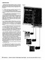
ECONORAM IXTo
USER'S MANUAL
M
3iK x 8 static memory
Digital Group Buss
using MM5257/TMS40L44 • "MHz
211 /
~
A
(OmpuKifMproduct from ®®@)m®!!!J~_---/
2179 mac
Table of contents
About Econoram IX. . . . . . . . . . . . . . . . . . . . . . . . . . . . . . . . . . . . . . . . . . . . . . . . . . . . . . . . . . . . . . . . . . . . . . . . 3
Technical overview. . . . . . . . . . . . . . . . . . . . . . . . . . . . . . . . . . . . . . . . . . . . . . . . . . . . . . . . . . . . . . . . . . . . . . . 3
Parts list. . . . . . . . . . . . . . . . . . . . . . . . . . . . . . . . . . . . . . . . . . . . . . . . . . . . . . . . . . . . . . . . . . . . . . . . . . . . . . . . . 3
Assembly procedures. . . . . . . . . . . . . . . . . . . . . . . . . . . . . . . . . . . . . . . . . . . . . . . . . . . . . . . . . . . . . . . . . . . . . 4
Component layout .... . . . . . . . . . . . . . . . . . . . . . . . . . . . . . . . . . . . . . . . . . . . . . . . . . . . . . . . . . . . . . . . . . . . . 5
Construction .................... . . . . . . . . . . . . . . . . . . . . . . . . . . . . . . . . . . . . . . . . . . . . . . . . . . . . . . . . . 6
Memory address assignment. . . . . . . . . . . . . . . . . . . . . . . . . . . . . . . . . . . . . . . . . . . . . . . . . . . . . . . . . . . . . . . 7
Block disable switches. . . . . . . . . . . . . . . . . . . . . . . . . . . . . . . . . . . . . . . . . . . . . . . . . . . . . . . . . . . . . . . . . . . . 7
Write enable switches. . . . . . . . . . . . . . . . . . . . . . . . . . . . . . . . . . . . . . . . . . . . . . . . . . . . . . . . . . . . . . . . . . . . . 7
Memory testing. . . . . . . . . . . . . . . . . . . . . . . . . . . . . . . . . . . . . . . . . . . . . . . . . . . . . . . . . . . . . .. . . . . . . . . . . . . 7
Logic diagram. . . . . . . . . . . . . . . . . . . . . . . . . . . . . . . . . . . . . . . . . . . . . . . . . . . . . . . . . . . . . . . . . . . . . . . . . . 8, 9
Memory testing routine. . . . . . . . . . . . . . . . . . . . . . . . . . . . . . . . . . . . . . . . . . . . . . . . . . . . . . . . . . . . . . . . . . .. 1a
Circuit description. . . . . . . . . . . . . . . . . . . . . . . . . . . . . . . . . . . . . . . . . . . . . . . . . . . . . . . . . . . . . . . . . . . . . . .. 11
Customer service information. . . . . . . . . . . . . . . . . . . . . . . . . . . . . . . . . . . . . . . . . . . . . . . . . . . . . . . . . . . . .. 1 2
Limited warranty information. . . . . . . . . . . . . . . . . . . . . . . . . . . . . . . . . . . . . . . . . . . . . . . . . . . . . . . . . . . . . .. 12
2
ECONORAM IX • COMPUKIT PRODUCT FROM GODBOUT ELECTRONICS • BOX 2355, OAKLAND AIRPORT, CA 94614
ABOUT ECONORAM IX
Congratulations on your choice of the ECONORAM IX, a
32K x 8 memory board designed specifically for electrical
and mechanical compatibility with the Digital Group buss.
AIIIC sockets, bypass capacitors, and other components,
are soldered on the board in order to eliminate the most
tedious and error-prone aspects of the assembly of this type
of kit. Assembly should take only an hour or so. We encourage you to take the time to familiarize yourself with the
featutes and the circuit design of the board prior to assembly. Several of the features - such as independent block
organization, easy switch assignment of blocks to the
desired memory address location, switch selectable block
disable and write protect - have been unavailable to Digital
Group System owners until now.
Upon completion of the board you will discover - as thousands of satisfied ECONORAM owners have discovered the pleasure of using a fine memory board that just works,
and works, and works.
As the first company to nationally offer memory kits to
computer hobbyists, we thank you for choosing ECONORAM
IX ... welcome to the club.
TECHNICAL OVERVIEW
This board incorporates proven static memory technology using industrial design techniques and generous
safety factors to avoid marginal operation.
Of the two currently popular approaches to memory
design - static and dynamic - static memories are the overwhelming choice in applications where speed, simplicity,
ease of use and reliability must be considered.
In order to retain data, dynamic memory must be continually refreshed. This board, due to its static design, will
retain data as long as power is applied. This is of particular
interest to Digital Group owners, since the Digital Group
system makes use of the unique ability of the Z-80 CPU to
take care of dynamic memory refresh rather than using
refresh circuitry on each individual memory board. Unfortunately, while this is a valid and economical approach, it
precludes the use of the normal system RESET or the use of
the WAIT line since the CPU cannot continue to refresh the
memory while RESET is held or CPU WAIT is used. For instance, in order to use the Digital Group disk controller with
dynamic memory, both the controller board and the CPU
board must be modified, an extra input port bit is required,
and special software is necessary. The Econoram IX is not
subject to the above problems because of its static design.
The individual memory chips used on this board are
grouped together to form four blocks of memory: two 4K
blocks, one 8K block and one 16K block. Each block may be
aSSigned to any of its respective boundaries (Le., either 4K
block to any 4K boundary, the 8K block to any 8K boundary
and the 16K block to any of the four 16K boundaries) by setting the starting address with the on-board'OIP switches (no
jumpers required). Additional features include a write-protect switch for the 16K block and disable switches for both
the 8K and 16K blocks. Also included are jumper pads for
adapting the board to non-standard polarities of the WRITE
strobe and the ROM strobe (the signal which disables the
board when the bootstrap EROM is being accessed). No
jumpers are required for standard Digital Group systems,
since traces have been provided to connect the pads for the
standard Signal polarities.
Extra heavy power supply traces, generous bypaSSing of
power supply lines, sockets for all integrated circuits,
careful layout and a double-sided, solder-masked printed
circuit board with complete component and switch legends
make this a versatile memory board which will give exceptionally long and trouble-free service.
,-- Parts List --------------,
Upon receipt of your kit, check your parts against the list below.
D
(1)
Econoram IX circuit board
D
D
D
D
D
INTEGRATED CIRCUITS (note: the following parts
may have letter suffixes and prefixes along with the
key numbers given below).
(64) MM5257 or TMS40L44 memories (U13-U76)
(5)
74LS04 hex inverter (U6-U1 2)
(1)
74LS32 quad 2-input OR gate (US)
(1)
7 4LS139 decoder / demultiplexer (U7)
(1)
74LS240 TRI-STATE$ buffer (U8)
(4)
74LS266 ex-NOR o.c. (U1-U4)
D
D
D
D
OTHER ELECTRONIC COMPONENTS
(2)
S.I.P. resistor packs (R1 , R2)*
(2)
2K7 ohm 1/4 watt resistors (red-violet-red R3, R4)*
(1)
39 p,F tantalum capacitor (C1)*
(28) ceramic capacitors*
D
D
D
MECHANICAL COMPONENTS
(76)
low profile sockets*
(2)
8 pole dipswitches (S1, S2)*
(1)
user manual
D
2/79
3
ASSEMBLY PROCEDURES
There is no soldering necessary to complete this kit,
proper operation depends upon correct identification and
handling of the parts used in its construction. Please read
this manual thoroughly before assembly.
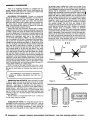
SOLDERING TECHNIQUES. Though no soldering
should be required to complete assembly, you may have to
'touch up' an occasional void; or (heaven forbid) even
replace a component at some future da.te. The E~onoram
board is solder-masked with a solder-resistant coating over
the entire board, except where solder connections are
made. This minimizes the chances of getting an unwanted
solder bridge between adjacent traces.
Those who have not previously worked with a soldermasked board will find that it takes considerably less solder
to make a good joint since the solder does not spread out
across the solder pad. On this board, all soldering should be
done on the solder side of the board (the back side or side
opposite the component side). Use a low wattage iron
(10-25 watts) with a small or 'PENCIL' tip. Use a good quality
rosin-core solder (,60/40 alloy'). Because of the close spacing of pads we recommend keeping the c?mpone~t leads
straight up while soldering (see figure 1). Bring the tiP of the
iron in at an angle, touching both the pad and the component
lead and feed a small amount of solder in at either side
whe;e the tip touches the pad and lead (see figure 2). Use
only enough solder to fill the joint and make a very small
'fillet' around the lead. Keep the soldering iron on the joint
only long enough to make sure that the solder has 'wetted'
the lead and flowed smoothly into the joint; too little time
may result in a poor joint and too much time may damage the
component or the bond between the pad and the board. Be
especially careful when soldering dipswitches, since some
internal parts are thermoplastic and are very heat sensitive.
Clip any excess leads off fairly close to the board to keep
them from bending over and touching anything. Use eye protection while soldering or clipping leads.
NO TE: The use of any type of solder other than a good
quality rosin-core solder invalidates the warranty. Do not us~
any type of solder paste or corrosive flux under any condItions.
ing across a rug or sliding into a chair on a dry day. If you
then touch the pins of an IC, this charge can flow through the
IC and damage its internal structure. Most static discharges
destroy the IC immediately, but it is possible for a low
energy static discharge to puncture the gate oxi~e in suc~ at
manner than the IC functions properly for a while but fall'
some time later as metal migrates into the puncture and
finally causes an internal short-circuit. To prevent this, leave
the ICs in their protective foil until needed. Then, before
plugging in each IC, touch an exposed trace on the board
(pin 1 or 2 on the edge connector, for instance) to equalize
any residual charge. This will force any charge to flow
through your body instead of through the pins of the IC. Also,
avoid wearing clothing which has a tendency to generate
static charges (such as sweaters, almost all synthetic
fabrics, and so on). (Industrial IC users recommend wearing
a grounded wrist strap and working on a conductive surface
-which is grounded to the same point. Almost the same protection can be achieved by working on a sheet of aluminum
foil which is electrically connected to the wrist with a flexible wire attached to a metal watch band or loop of bare wire
around the wrist. If the aluminum foil can be conveniently
grounded it will over even more protection).
•••
do not bend
leads over
lead
component
Figure 1.
r-------------------------------------,
Any modification of this board not approved in :
:
I
~
:
advance by Godbout Electronics may void your J :
_____________________________________
warranty.
I
IDENTIFICATION OF PARTS. There are many ICs used
in this kit· each one must be oriented correctly for proper
operation: Most ICs have a dot near one. corner that ind.icates pin 1 (see figure 3). Sometimes. this dot appears. In
conjunction with a deeply cut notch or circle. Other types indicate the pin 1 end of the IC by a deep notch or a notch
within a shallow circle (see figure 4). In case of doubt, place
the IC in front of you so that any identifying numbers read
from left to right; pin 1 is almost always in the lower left-hand
corner (figure 5).
NOTE: If there is a recognizable mark for pin 1, always go
by that rather than the printing.
Figure 2.
notch
dot
pin 1
pin 1
pin 1
HANDLING OF PARTS. All integrated circuits may be
damaged by static electricity; however, MaS ICs - such as
the memory ICs included with this kit - are more vulnerable
than most. You can easily accumulate a static charge on
your body in the thousands-of-Volts range by merely walk-
4
Figure 5.
Figure 3.
Figure 4.
ECONORAM IX . COMPUKIT PRODUCT FROM GODBOUT ELECTRONICS· BOX 2355, OAKLAND AIRPORT, CA 94614
II.)
.....
....
CD
Component Layout
CONSTRUCTION
Keeping the preceding information in mind, it is now time
to mount the various components and install the ICs into their
sockets. Orient the board as shown in the component layout;
then referring to this layout, follow the steps below in the
order given.
Figure 6
o
1. Before inserting any components, check for any short
circuits in the power distribution lines as follows:
A. If you are working on a conductive surface, insulate
the board with a sheet of cardboard or other non-conducting
material.
B. If the dipswitches on your board have already been
installed, flip each switch to the OFF position.
C. Measure the resistance between pins 1 and 2 of the
edgeboard connector with an ohmmeter (see figure 6a). The
resistance should be (nearly) infinite. A reading below
around 3000 ohms indicates a bad switch element and a
reading near a ohms indicates an 'etch bridge' or solder
bridge between the +5 and ground traces or (less likely) a
shorted bypass capacitor.
o
2. The board is shipped configured for an 'active low'
memory write strobe and an 'active low' ROM access strobe
("PHANTOM" line in S-1 00 Systems). If you have a standard
Digital Group system, skip this step. If you are assembling
your board for use in a non-standard system, proceed as
follows:
A. To configure the board for an 'active high' memory
write strobe, cut the trace between 'c' and 'w bar' (w) and install a jumper between 'c' and ow' (see figure 6b).
B. To configure the board for an 'active high' ROM
access strobe (the signal which disables RAM when the
ROM is being accessed), cut the trace between 'c' and 'r bar'
('f)and install a jumper between 'c' and Or' (see figure 6c).
o
3. If you have a conductive work surface, remove the
material which was insulating the board from it. All of the ICs
should be oriented so that the pin 1 end is toward the left
side of the board. Any numbers or other markings should normally be right side up with the board oriented normally (as
shown in the component layout diagram). If any markings are
upside-down, the IC may not be correctly installed.
A common problem with boards returned for repair is improper installation of an IC. Sometimes a pin will bend under
the IC instead of going into the proper socket contact. We
recommend inserting each IC halfway and verifying visually
that all pins are started into the socket. Then, push the IC in
the rest of the way.
Keeping this in mind, first insert the support ICs and then
all of the memory ICs.
o 4. Check the board over carefully for errors in construction. If all appears correct, assembly of your board is complete. Refer to the following sections for instructions on address selection and switch-selectable options.
6
Figure 6a
Figure 6c
ECONORAM IX . COMPUKIT PRODUCT FROM GODBOUT ELECTRONICS· BOX 2355, OAKLAND AIRPORT, CA 94614
MEMORY ADDRESS ASSIGNMENT
WRITE ENABLE SWITCH
This board is configured as two 4K blocks, one 8K block
and one 16K block. Each 4K block may be assigned to any
wea of memory beginning on a 4K boundary (OK, 4K, 8K,
~K, etc.). The 8K block may be assigned to any 8K boundary (OK, 8K, 32K, 40K, etc.) and the 16K block on any 16K
boundard (OK, 16K, 32K or 48K). The only other limitation is
that the assigned locations should not overlap each other or
any other RAM in your system.
NOTE: In the following table, S1 is the first dipswitch and
S2 if the second dips witch. Each dipswitch has eight individual switch sections numbered 1 through 8. "0" = switch
off and "1" = switch on. S2-4, -7 and -8 are not used for address selection and are explained in the next section.
Switch S2-8 is the WRITE ENABLE switch for the 1 6K
("Oil) block of memory. This switch should be ON for normal
operation. However, if the switch is placed in the OFF position after data has been written into this block, the block will
be WRITE PROTECTED and the data can be read but not
changed. This is a very powerful tool for program development and debugging, since the data in the write protected
block cannot be destroyed by a wayward program. You must
remember, however, that data buffers which must be
changed by the program must reside outside the protected
area.
MEMORY TESTING
ST ARTING ADDRESS
SWITCH POSITION
BLOCK A, B
hex
OK
4K
8K
12K
16K
20K
24K
28K
32K
36K
40K
44K
48K
52K
56K
60K
0000
1000
2000
3000
4000
5000
6000
7000
8000
9000
AOOO
BOOO
COOO
0000
EOOO
FOOO
(split octal)
(0001000)
(0201000)
(0401000)
(0601000)
(1001000)
(1201000)
(1401000)
(1601000)
(2001000)
(2201000)
(2401000)
(2601000)
(3001000)
(3201000)
(3401000)
(3601000)
C
0
4K
8K
16K
A: S1-:1 234 S2-:123 S2-:56
B: S1-:5678
0000
000
00
0001
0010
001
0011
010
01
0100
0101
011
0110
0111
10
1000
100
1001
101
1010
1011
110
11
1100
1101
1110
111
1111
NO TE: If the desired starting address is represented as a
binary number, the switch setting represents the 2, 3, or 4
most significant bits of that address. Once you become
familiar with the addresses of the various boundaries, you
will find it easy to re-assign various boundaries, you will find
it easy to re-assign memory blocks without referring to the
above table.
BLOCK DISABLE SWITCHES
Switch S2-4 and S2-7 are disable switches for the 8K
("C") block and the 16K ("0") block respectively. These
switches should be OFF for normal operation. If either switch
is moved to the ON position, the corresponding block is
effectively removed from memory (although as long as
power is maintained, data previously stored in the block is
not disturbed and may be re-accessed by returning the
switch to the OFF position). This feature is primarily
designed to allow the use of a partially populated board (any
block without a full complement of memory ICs must be disabled to prevent conflicts if other RAM in the system is
assigned an address which overlaps that of the incomplete
ilock). However, the disable switch can also be used as an
,id in trouble-shooting and as a pseudo write-protect to protect a section of code while de-bugging another program.
An excellent memory testing routine is distributed by the
Digital Group which will test both the data integrity and the
speed of the memory. If this is unavailable to you, we have included a test route (page 10) which gives the board a somewhat slow but thorough workout. It can be entered in
machine code through the programming options in your
operating system or in source code through an assembler
(to use the Digital Group Assembler the mnemonics must be
changed from INTEL 8080 mnemonics to Zilog Z-80
mnemonics).
The routine is initially set up to test a 32K segment of
memory starting at 4000 hex and ending at BFFF hex. The
starting address may be changed by entering the desired
start address at 3001 and 3002 hex (low byte first). The ending address may be changed by entering the high byte of the
address following the last tested byte at 3004 hex (if the test
is to end at E7FF hex, enter E8 at 3004).
If the memory passes the test, it starts over again. Three
bytes have been left open at "MARK" (3039 hex) to enable
you to insert a call to a routine to display the test address if
desired.
If any portion of memory fails the test, critical information
is stored and the routine enters an endless loop at "SHL Til
(3070 hex). This "jump to itself" may be replaced by a "jump
to a routine" which notifies you of the failure, or the loop may
be terminated by a RESET to your monitor, from which you
can examine the following locations where the information
regarding the failure is stored:
3069
306A
306B
3060
306E
"FOE"
"FDE"+1
"FHL"
"FOUT"
"FIN"
test character
fill character
failure address (low-high)
data expected at this address
data read from this address
The difference between "FOUT" and "FIN" should indicate which bit is failing, and together with "FHL" should
point to the bad memory IC. If several bits are different, the
problem could be an address decoding problem caused by
the failure of one of the support chips.
2/79
7
A15
A14
Ul~
A11~MA11
A13
A12
UUJ
A10~Mii10
ECONORAM IX
PAGE
1
OF
2
Ul~
A9~Mii9
R1
R1
U10
A8~Mii8
51-1
U12
A7~Mii7
51-2
U12
A6~MA6
51-3
"X)-----_--_
13
12
IT
A5
Ail
U
MA 5
~-
U12
AA~Mii4
51-4
U12
A3~Mii3
R2
R1
U12
A2~MA2
un
_
51-5
AT~MA1
51-6
A0~MA0
un
51-7
U9
007~M017
51-8
U9
006~M016
U9
005~M015
R2
R2
U7
=>
c..
u
:E
U9
_
004~M014
U9
52-1
~ D03~MD13
52-2
D02~MD12
52-3
DO 1 K
U9
~
U18
1
2
MD I 1
DOil~MD19J
52-4
R2
R2
U7
52-5
017
1)16
01 5
52-6
o-_ _ _ _ _ _ _ _ _ _ _ _ _ _ _~-~ll~
U6
~~~~~r+--~G1
014
=>
c..
u
':"
013
LR
r:oRr
012
01 1
R3
010
!_··_··_··_·Lq_
. .6'-/
.
ROM 1/0,l9_ _ _ _ _ _ _ _ _ _ _ _':"
__
~ 11~---------------------~------------+------~/u.J~
~~--~-V-C-C-------;~1~::~:-2-1------------~{~o-~~~-----~~~~-~~-S-~-:--I-R2--·::.B.~
8
ECONORAM IX . COMPUKIT PRODUCT FROM GODBOUT ELECTRONICS· BOX 2355, OAKLAND AIRPORT, CA 94614
0
~
OMI0-----.
MOl
1----.
~IX----.-.l.
11
r
,..--O....
IN-....
DIN
12
MAll
-1
--I
-i
MA 10
MAg
--i
--i
-i
MA8
MA7
MA6
OOUT
MA5
7
-DIN - - ,
I
--I
--I
MAl
MA0
CE
WE
CE
MOO 1
WE
OOUT
I
I
I
I
I MOO X
-I
W\2
I
OOUT
--i
MA 4
MA3
DIN
I
I
II
5 CHIPS
SIMILARLY
ARRANGED
--i
DOUT
MOl 7
--I
CE
WE
MOO
7
OF
2
8
CEX-----I---+-----......--+-----.....~~~~------I
WE X
PAGE
2
BIT POSITJ.ON
1
3
2
4
5
7
6
WE A,B,C --,.
A~
-
CE A~
~
B~
-
CE B0
~
-
C~
-'"
CE C0
-
-CE C1
C1
WE D.......
D~
-""
CE00·
~
D1
-CE 01
~
-CE 02
D2
.
-CE 03
D3
,
--1 tJ
~oo
t
1
MOO 1
~·1DI It'
t..1 t 1 t
MDO 2
MOll
MOO 3
MDI 2
ARRAY CONSISTS OF
+5
MOl 3
1
MOO 4
t..! t-11-11
"MDI
~1DO 5
MOl 4
MOO 6
MOl 5
MOO 7 _
6
~1DI 7
64 (1 x 4096) STATIC RAMS
~-----------~----__
+lc1
I
3g
uF/1o
TANT CAP
I1_~8~lsc _1T
CAPS
GNO~----------+-----~~------~
2/79
9
MEMORY TESTING ROUTINE
3000
3003
312185
30e8
300A
3e0S
380C
300£
3010
3013
3014
3015
3816
3017
3818
3019
381C
381D
381£
3"IF
3022
3025
3026
3027
3028
302B
302C
302D
382£
3031
3e32
3833
3036
3039
383A
383B
383C
303F
3040
3043
3044
3045
3047
3049
304A
3e4D
3058
3e51
3052
3e55
3056
3e59
3e5A
305B
30SC
3eSF
3062
3865
3e67
3069
3e6B
306D
3e6E
3e6F
3072
312175
3076
3879
307A
3870
3080
21
3E
32
3E
00 40
A0
6E 30
1121
81&
4F
16
IE
22
AF
47
7S
SA
57
79
2A
72
23
BC
C2
2A
73
7S
BE
C2
79
23
94
C2
B8
44
CA
3A
Ii"
88
"0
3A
B9
CA
79
67
2E
C6
4F
C3
22
7A
BE
C2
2C
C2
79
24
BC
C2
2A
C3
22
32
7E
32
EB
22
C3
00
FF
65 3121
65 30
IC 30
65 38
6F 38
4D 30
15 30
66 30
6£ 30
e0 30
00
Ie
.0 30
67 3e
6F 30
51 3e
50 3e
67 3e
25 38
6B 38
6D 30
6E 3e
69 30
70 30
0010
0020
012130
012140
012150
0060
0070
0080
0090
0100
8110
0120
121138
0140
0150
0168
0170
0180
0190
0200
0210
0228
0230
0240
0250
0268
827e
0288
0290
e300
0310
0328
0325
0338
0331
0332
0340
0350
036e
0370
0380
0398
e4ee
e41e
1211&20
0430
e440
e45121
e46e
el&70
048e
el&90
0500
0510
052e
e53e
eS4e
12J55e
056e
0570
0580
e590
0680
061121
0620
063121
0640
0650
0660
067121
0680
STRT LXI HI4000H
END MVI A,0A0H
STA FIN
MVI A,18H
ADD H
MOV C,A
MVI
DI0
MVI E,I2JFFH
DONE SHLD STAD
XRA A
MOV B,A
SCND MOV AlE
MOV £,D
MOV DIA
MOV A,C
LHLD STAD
FILL MOV MID
INX H
CMP H
JNZ FILL
LHLD STAD
NEXT MOV H,£
MOV A,£
CMP M
JNZ FAIL
MOV A,C
INX H
SUS H
JNZ NDON
CMP B
MOV BIH
SCND
JZ
LDA STAD+l
MARK NOP
NOP
NOP
LDA FIN
CMP C
JZ
STRT
MOV A,C
MOV HIA
MVI LI0
ADI
10H
MOV C,A
DONE
JMP
NDON SHLD NXAD
LOPS MOV A,O
LOPA CMP M
JNZ FAIL
INR L
JNZ LO~A
MOV A,C
INR H
CMP H
JNZ LOPS
LHLD NXAD
JMP NEXT
STAD OS
2
NXAD DS
2
FDE OS
2
FHL OS
2
FOUT OS
1
FIN OS
1
FAIL SHLO FHL
STA FOUT
HOV AIM
STA FIN
XCHG
SHLD FOE
SHLT JMP SHLT
r-----
SUGGESTED ADDITIONS TO DIGITAL GROUP
-----1
Z·80 CPU BOARD ...
The following comments and fixes have been reported to
us by digital group users:
The data lines from memory to the CPU are not terminated
on the Digital Group Z-80 CPU board, and because of this
the CPU will occasionally get a data byte other than "FF"
when accessing a non-existent memogxkmtqkuwxvs with
programs (such as the Digital Group Memory Test Routines)
which use this to find memory limits. These lines should be
pulled up to +5 through 2.7K resistors (3.9K and 4.7K resistors have been used with satisfactory results). A convenient
location to install these pullup resistors is on the left-hand
side of the CPU board. Above each 2102 location in the first
column of IC's two unused plated-through holes are provided (for undershoot clamping diodes). The right-hand hole
is connected to its respective data line. Also, on the left side
of each of these 2102's are two unused plated-through holes
for bypass capacitors. The pullup resistors may be connected from the top hole (+ 5) of each of these pairs to the
right-hand diode pad (data line) above each 2102.
There is an occational glitch on the "WRITE" line of some
Z-80's which, if not corrected, can be a problem. With memory (such as this board) fast enough to respond to it, the glitch
can write garbage into whichever location happens to be on
the address buss at the time. The problem can be easily corrected by the addition of a 100 pF capacitor between pin 22
of the Z-80 and ground on the CPU board. Two platedthrough holes connected to these lines are conveniently 10cated near the lower right corner of the Z-80 and may be
used to install the capacitor.
Although the above problems may not be noticeable on
your system, we feel that the addition of the recommended
fixes will add an extra measure of reliability to it and perhaps
help you to avoid those inexplicable program crashes.
* These mods will help any system, but are mandatory for
successful 4MHz operation.
diode pads
ground'Wrl
~ ___ dataline
bypass
cap. pads -....:...
I 21~
o I
I
~
o I
~
ground
pullup resistors
(8 required)
2102
memory to CPU
data line pullup
resistors
2.7K to 4.7K
2102
~
I
2102
*
10 ECONORAM IX • COMPUKIT PRODUCT FROM GODBOUT ELECTRONICS.
BOX 2355, OAKLAND AIRPORT, CA 94614
I
I
I
•
Data to be written into a memory location is buffered and
to the data in pins of each column of memory ICs.
However, when a memory write strobe is received from the
CPU, the data is loaded into the addressed location of the
enabled row of ICs only.
When the output of a logic Ie changes state, it draws a
very short high-current 'spike' from the power lines. If
unchecked, the electrical noise created by these transient
spikes might couple into the logic lines and cause erratic
operation of the board. To absorb these transients, bypass
capacitors are liberally placed across the power distribution
lines throughout the memory array and at every support IC.
This board is guaranteed to operate at 4.0 MHz over the
full temperature range 0° to 70° C. and to draw less than
3500 mA (3.5 amps). The typical measured current draw is
less than 3000 mA at cold start-up, rapidly decreasing to
around 2400 to 2800mA as the board warms up.
It is interesting to note that static RAM technology has
progressed to the point at which this high performance static
RAM board is comparable in cost and power consumption to
dynamic memory boards.
present~d
to pin 22
(WRITE)
r
Z-80
~
' - -_ _ _....J
I
Z-80 WRITE line
.. '
"'grOUnd
'--------------------------~---------------~
CIRCUIT DESCRIPTION
The heart of ECONORAM IX is the MM5257 -3L or
TMS40L44-25 memory IC (RAM), which can store 4096 bits
("4K" bits) of information (thus, each is a "4K x 1" memory
IC). These are not standard MM5257/TMS40L44's, the
memory ICs included in this kit are specifically tested and
designated by the manufacturer as low power, high speed
parts.
, These ICs are arranged in rows that are 8 ICs wide - each
IC contributing one bit of an a-bit byte. Thus each row can
store 4K x 8 bits (4K bytes). By connecting 8 of these rows
together in parallel, a total of 32K bytes of memory storage
is produced. (Note that the bit number corresponding to a
given column of ICs is indicated along the top edge of the
memory array and the row number corresponding to the 4K
segment within a given block is indicated along the right
hand edge of the array).
Now that we have this storage, there are other aspects to
consider in order to be able to make use of it: First, addressing a specific location in memory; and second, writing data
into the memory or reading data from it.
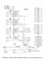
The logic diagram on pages 8 and 9 show the address
decoding, read/write control, memory array, input buffering
and output buss driver circuits for the Econoram IX. Each row
of memory les requires 12 address bits (AO-A 11) to select
one unique location of the 4096 available locations. These
bits are brought onto the board through inverting buffers (so
as to present only one low-power TTL load to the buss) and
distributed to the '1 2 address select pins on each of the
memory ICs. The remaining 4 address bits are also buffered/
decoded, and if they represent a valid address for the board
(as determined by the settings of the address select
switches), used to enable the appropriate row of memory
les.
When a row of ICs is thus enabled, it presents the data
byte stored at the addressed location to the output buss
driver. This IC is normally in a high-impedance state (essentially disconnected). When a valid address has been
~ceived and a MEMORY READ strobe is received from the
~PU, the output driver places the selected data onto the
data buss to the CPU.
THANK YOU
This board is the result of much time, work and experience on the part of a number of people. In addition to
thanking you for choosing this board, we'd like to thank the
Phantom* and many others for their help with this project.
We strive for a board that doesn't just work the first time,
but continues to give reliable operation for a long time. If we
can be of any help to you in applying this board, or if you
have any questions, please let us know. As always, we
solicit your comments, letters and new product suggestions.
HAPPY COMPUTING!
*Editor's Note: 'THE PHANTOM' is Doug Bell, who provided the impetous for producing this kit and then wrote
these instructions using a word processor/text editor on his
Digital Group System which included prototypes of this
memory and a disk system of his own design.
2/79
11
CUSTOMER SERVICE INFORMATION
Our paramount concern is that you be satisfied with any Godbout
CompuKit product. If this product fails to operate properly, it may be
returned to us, see warranty information below.
If you have any questions about assembly, performance, specifications or need further information feel free to write us at:
P~O.
Box 2355, Oakland Airport, CA 94614.
When writing, please be as specific as possible concerning the nature
of your query. We maintain a 24 hour a day phone, for taking orders,
(41 5) 562-0636. If you have problems or questions which cannot be
handled by mail, this number can be used to connecl you with our technical people ONLY during normal business hours (10am-5pm Pacific
Time). Unfortunately, we cannot return calls, or accept collect calls.
LIMITED WARRANTY INFORMATION
Godbout Electronics will repair or replace, at our option, any parts
found to be defective in either materials or workmanship for a period of 1
year from date of invoice. Defective parts must be returned for replacement.
If a defective part or design error causes a Godbout Electronics pro-duct to operate improperly during the 1 year warranty period, we will
service it free (original owner only) if delivered and shipped at owner's
expense to Godbout Electronics. If improper operation is due to an error
or errors on the part of the purchaser, there may be a repair charge.
Purchaser will be notified if this charge exceeds $10.00.
We are not responsible for damage caused by use of solder intended
for purposes other than electronic equipment construction, failure to
follow printed instructions, misuse or abuse, unauthorized modifications, use of our products in applications other than those intended by
Godbout Electronics, theft, fire, or accidents.
~eturn to purchaser of a fu IIy functioning unit meeting all advertised
specifications in effect as of date of purchase is considered to be complete . fulfillment of all warranty obligations assumed by Godbout
Electronics. This warranty covers only products marketed by Godbout
Electronics and does not cov~. other equipment used in conjuncti6n
with said products. We are not ~sponsible for incidental or consequential damages.
Prices and specifications are subject to change without notice, owing
to the volatile nature and pricing structure of the electronics industry.
-
"Econoram" and "Econoram IX" are trademarks of W. J. Godbout.
TRI-STATE~
is a trademark of National Semiconductor Corp.
Contents of this booklet @>1979 by Godbout Electronics. All rights
reserved. We encourage quotation for the purposes of product review
if source if credited.
12
ECONORAM IX . COMPUKIT PRODUCT FROM GODBOUT ELECTRONICS • BOX 2355, OAKLAND AIRPORT, CA 94614