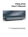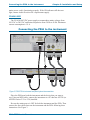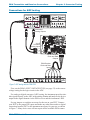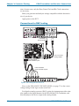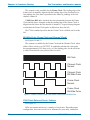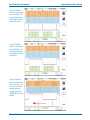
1
PSIA-2722
User’s Manual
Installation and Operation of the Audio Precision
Programmable Serial Interface Adapter
Copyright Ó 2002-2005 Audio Precision, Inc.
All rights reserved.
Audio Precision part number 8211.0159 Rev 1
No part of this manual may be reproduced or transmitted in any
form or by any means, electronic or mechanical, including
photocopying, recording, or by any information storage and
retrieval system, without permission in writing from the
publisher.
Audio Precision®, System One®, System Two™, System Two
Cascade™, System One + DSP™, System Two + DSP™, Dual
Domain®, FASTTEST®, APWIN™, 2700 Series, AP2700,
ATS™ and ATS-2™are trademarks of Audio Precision, Inc.
Windows is a trademark of Microsoft Corporation.
Published by:
5750 SW Arctic Drive
Beaverton, Oregon 97005
Tel: 503-627-0832
Fax: 503-641-8906
US Toll Free: 1-800-231-7350
email: [email protected]
Web: audioprecision.com
Printed in the United States of America
V0126110928
Contents
Safety Information . . . . . . . . . . . . . . . . . . . . . . . . . . . . . . v
Safety Symbols . . . . . . . . . . . . . . . . . . . . . . . . . . . . . . . vi
Chapter 1
Introduction . . . . . . . . . . . . . . . . . . . . . . . . . . . . . . . . . 1
Capabilities . . . . . . . .
Transmitter and Receiver
Data and Clock ports . .
Data settings . . . . . .
Voltage levels . . . . . .
Documentation. . . . . . .
.
.
.
.
.
.
.
.
.
.
.
.
.
.
.
.
.
.
.
.
.
.
.
.
.
.
.
.
.
.
.
.
.
.
.
.
.
.
.
.
.
.
.
.
.
.
.
.
.
.
.
.
.
.
.
.
.
.
.
.
.
.
.
.
.
.
.
.
.
.
.
.
.
.
.
.
.
.
.
.
.
.
.
.
.
.
.
.
.
.
.
.
.
.
.
.
.
.
.
.
.
.
.
.
.
.
.
.
.
.
.
.
.
.
.
.
.
.
.
.
.
.
.
.
.
.
.
.
.
.
.
.
.
.
.
.
.
.
.
.
.
.
.
.
.
.
.
.
.
.
2
2
2
3
3
4
Chapter 2
Installation and Setup . . . . . . . . . . . . . . . . . . . . . . . . . . . 5
PSIA-2722 Components . . . . . . . .
Power Supply . . . . . . . . . . . .
PN 4540.0020. . . . . . . . . . .
PN 4540.0051. . . . . . . . . . .
Connecting the PSIA to the instrument
.
.
.
.
.
.
.
.
.
.
.
.
.
.
.
.
.
.
.
.
.
.
.
.
.
.
.
.
.
.
.
.
.
.
.
.
.
.
.
.
.
.
.
.
.
.
.
.
.
.
.
.
.
.
.
.
.
.
.
.
.
.
.
.
.
.
.
.
.
.
.
.
.
.
.
.
.
.
.
.
.
.
.
.
.
.
.
.
.
.
.
.
.
.
.
6
6
6
7
7
Chapter 3
Converter Testing. . . . . . . . . . . . . . . . . . . . . . . . . . . . . . 9
Relationship between PSIA and the instrument
PSIA Transmitter and Receiver Connections . .
Connect an oscilloscope . . . . . . . . . . .
Connections for Loop-Back configuration . .
Connections for ADC testing . . . . . . . . .
Connections for DAC testing . . . . . . . . .
Connections for SRC testing . . . . . . . . .
The Transmitter and Receiver panels . . . . .
Transmitter and Receiver Settings . . . . . .
PSIA-2722 User’s Manual
.
.
.
.
.
.
.
.
.
.
.
.
.
.
.
.
.
.
.
.
.
.
.
.
.
.
.
.
.
.
.
.
.
.
.
.
.
.
.
.
.
.
.
.
.
.
.
.
.
.
.
.
.
.
.
.
.
.
.
.
.
.
.
.
.
.
.
.
.
.
.
.
.
.
.
.
.
.
.
.
.
.
.
.
.
.
.
.
.
.
.
.
.
.
.
.
.
.
.
.
.
.
.
.
.
.
.
.
.
.
.
.
.
.
.
.
.
.
.
.
.
.
.
.
.
.
10
11
11
11
13
14
15
17
18
i
Duplicated Controls and Displays . . . . . . . . . . . . .
Channel Data Assignment . . . . . . . . . . . . . . . . .
One-click I2S bus settings . . . . . . . . . . . . . . . . .
Transmit Data Clock Edge . . . . . . . . . . . . . . . . .
PreEmphasis (Transmitter only) . . . . . . . . . . . . . .
DeEmphasis (Receiver only) . . . . . . . . . . . . . . . .
Scale Freq. by . . . . . . . . . . . . . . . . . . . . . . .
Audio frequency scaling . . . . . . . . . . . . . . . . .
Rate Ref . . . . . . . . . . . . . . . . . . . . . . . . . .
Channel Data . . . . . . . . . . . . . . . . . . . . . . .
Bits per channel display . . . . . . . . . . . . . . . . .
MSB first: Transmitter . . . . . . . . . . . . . . . . . .
MSB first: Receiver . . . . . . . . . . . . . . . . . . .
Data and padding controls . . . . . . . . . . . . . . . .
Data . . . . . . . . . . . . . . . . . . . . . . . . . . .
Pads . . . . . . . . . . . . . . . . . . . . . . . . . . .
Left and Right Justify: Transmitter . . . . . . . . . . . .
Left and Right Justify: Receiver . . . . . . . . . . . . .
Pad bits logic states (Transmitter only) . . . . . . . . .
Data Bit Indicators . . . . . . . . . . . . . . . . . . . .
The Clocks control matrix . . . . . . . . . . . . . . . . .
The Clock signals . . . . . . . . . . . . . . . . . . . .
The Clock controls . . . . . . . . . . . . . . . . . . . . .
Direction . . . . . . . . . . . . . . . . . . . . . . . . .
Bit Clock Edge Sync (Frame Clock and Channel Clock).
Invert Waveform (Frame, Channel and N*Fs Clocks) . .
Shift One Bit Left (Frame Clock Only) . . . . . . . . . .
Bit Wide Pulse (Frame Clock and Channel Clock). . . .
PSIA Clock Rate and Factor Settings . . . . . . . . . .
Frame Clock (Fs) Rate Setting . . . . . . . . . . . . .
Channels per Frame . . . . . . . . . . . . . . . . . . .
Setting the Bits per Channel . . . . . . . . . . . . . . . .
N, the N*Fs multiplier . . . . . . . . . . . . . . . . . . .
M, the Master Clock multiplier . . . . . . . . . . . . . . .
Jittering the Master Clock . . . . . . . . . . . . . . . . .
Computed Clock Rate Displays . . . . . . . . . . . . . .
Logic Voltage controls . . . . . . . . . . . . . . . . . . .
PSIA Quick Setup Guide . . . . . . . . . . . . . . . . . . .
Common converter testing configurations . . . . . . . . . .
PSIA Transmitter: Frame, Bit & Master Clock OUT . . . .
PSIA Transmitter: Frame & Bit Clock OUT, Master Clk IN .
PSIA Receiver: Frame, Bit & Master Clock OUT . . . . . .
PSIA Receiver: Frame & Bit Clock OUT, Master Clock IN .
ii
.
.
.
.
.
.
.
.
.
.
.
.
.
.
.
.
.
.
.
.
.
.
.
.
.
.
.
.
.
.
.
.
.
.
.
.
.
.
.
.
.
.
.
.
.
.
.
.
.
.
.
.
.
.
.
.
.
.
.
.
.
.
.
.
.
.
.
.
.
.
.
.
.
.
.
.
.
.
.
.
.
.
.
.
.
.
.
.
.
.
.
.
.
.
.
.
.
.
.
.
.
.
.
.
.
.
.
.
.
.
.
.
.
.
.
.
.
.
.
.
.
.
.
.
.
.
.
.
.
.
.
.
.
.
.
.
.
.
.
.
.
.
.
.
.
.
.
.
.
.
.
.
.
.
.
.
.
.
.
.
.
.
.
.
.
.
.
.
.
.
.
.
.
.
.
.
.
.
.
.
.
.
.
.
.
.
.
.
.
.
.
.
.
.
.
.
.
.
.
.
.
.
.
.
.
.
.
.
.
.
.
.
.
.
.
.
.
.
.
.
.
.
.
.
.
.
.
.
.
.
.
.
.
.
.
.
.
.
.
.
.
.
.
.
.
.
.
.
.
.
.
.
.
.
.
.
.
.
.
.
.
.
.
.
.
.
.
.
.
.
.
.
.
.
.
.
.
.
.
.
.
.
.
.
.
.
.
.
.
.
.
.
.
.
.
.
.
.
.
.
.
19
20
20
21
22
22
22
22
22
23
23
24
24
25
25
25
26
26
26
26
27
27
27
28
28
28
29
30
30
31
31
32
32
33
33
33
34
34
36
36
36
37
37
PSIA-2722 User’s Manual
Appendix A
Miscellany . . . . . . . . . . . . . . . . . . . . . . . . . . . . . . . . . 39
PSIA Abbreviations and Terms . .
Oscilloscope Examples. . . . . .
N*Fs Table . . . . . . . . . . . .
Using INTERVU with PSIA-2722 .
.
.
.
.
.
.
.
.
.
.
.
.
.
.
.
.
.
.
.
.
.
.
.
.
.
.
.
.
.
.
.
.
.
.
.
.
.
.
.
.
.
.
.
.
.
.
.
.
.
.
.
.
.
.
.
.
.
.
.
.
.
.
.
.
.
.
.
.
.
.
.
.
.
.
.
.
.
.
.
.
.
.
.
.
39
40
42
42
Appendix B
Configuration Examples and Files . . . . . . . . . . . . . . . . . . . 43
Eval boards and sample files . . . . . . . . . . . . . . . . . . . . . . . . 43
Appendix C
Connection Guidelines . . . . . . . . . . . . . . . . . . . . . . . . . . 45
General Guidelines . . . . .
Oscilloscope Monitoring . .
Triggering . . . . . . . .
Oscilloscope Connections
.
.
.
.
.
.
.
.
.
.
.
.
.
.
.
.
.
.
.
.
.
.
.
.
.
.
.
.
.
.
.
.
.
.
.
.
.
.
.
.
.
.
.
.
.
.
.
.
.
.
.
.
.
.
.
.
.
.
.
.
.
.
.
.
.
.
.
.
.
.
.
.
.
.
.
.
.
.
.
.
.
.
.
.
.
.
.
.
.
.
.
.
.
.
.
.
45
45
46
46
Appendix D
Specifications . . . . . . . . . . . . . . . . . . . . . . . . . . . . . . . 47
DC Characterisics . . . . . . . .
DC characteristics, no load. . .
PSIA input / output impedance .
AC characteristics . . . . . . . .
Maximum clock frequency . . .
Output latency, Clock to Out . .
Setup and Hold, inputs . . . . .
User test jacks . . . . . . . . .
APIB . . . . . . . . . . . . . . .
APIB configuration maximums .
.
.
.
.
.
.
.
.
.
.
.
.
.
.
.
.
.
.
.
.
.
.
.
.
.
.
.
.
.
.
.
.
.
.
.
.
.
.
.
.
.
.
.
.
.
.
.
.
.
.
.
.
.
.
.
.
.
.
.
.
.
.
.
.
.
.
.
.
.
.
.
.
.
.
.
.
.
.
.
.
.
.
.
.
.
.
.
.
.
.
.
.
.
.
.
.
.
.
.
.
.
.
.
.
.
.
.
.
.
.
.
.
.
.
.
.
.
.
.
.
.
.
.
.
.
.
.
.
.
.
.
.
.
.
.
.
.
.
.
.
.
.
.
.
.
.
.
.
.
.
.
.
.
.
.
.
.
.
.
.
.
.
.
.
.
.
.
.
.
.
.
.
.
.
.
.
.
.
.
.
.
.
.
.
.
.
.
.
.
.
.
.
.
.
.
.
.
.
.
.
.
.
.
.
.
.
.
.
.
.
47
47
47
48
48
48
49
49
49
49
Appendix E
AP Basic Extensions for PSIA . . . . . . . . . . . . . . . . . . . . . 51
PSIA-2722 User’s Manual
iii
:
iv
PSIA-2722 User’s Manual
Safety Information
Do NOT service or repair this product unless properly qualified. Servicing
should be performed only by a qualified technician or an authorized Audio
Precision distributor.
One of two external power supplies is provided with this product:
The power supply PN 4540.0020 is designed to operate only from an AC
power source (100 V–240 V rms, 47 Hz–63 Hz) with an approved three-con ductor power cord and safety grounding. Do NOT defeat the safety ground
connection.
The power supply PN 4540.0051 is designed to operate only from an AC
power source (100 V–240 V rms, 50 Hz–60 Hz). This power supply has an in tegral 2-conductor mains plug.
Either power supply automatically adjusts to the line voltage and frequency
within the specified range. No user adjustments are necessary. Neither of the
power supplies nor the PSIA-2722 contain user-replaceable fuses.
Use only the AP power supply PN 4540.0020 or PN 4540.0051 with the
PSIA-2722. The use of other power supplies may result in damage to the
PSIA-2722, electrical shock hazard from the power supply or the PSIA-2722,
and loss of fire hazard protection.
This product and power supply are for indoor use ONLY.
PSIA-2722 User’s Manual
v
Safety Symbols
The following symbols may be marked on the panels or covers of equipment or modules, and may be used in this manual:
WARNING!—This symbol alerts you to a potentially hazardous condition,
such as the presence of dangerous voltage that could pose a risk of electrical
shock. Refer to the accompanying Warning Label or Tag, and exercise extreme
caution.
ATTENTION!—This symbol alerts you to important operating considerations or a potential operating condition that could damage equipment. If you
see this marked on equipment, consult the User’s Manual or Operator’s Manual for precautionary instructions.
FUNCTIONAL EARTH TERMINAL—This symbol marks a terminal that
is electrically connected to a reference point of a measuring circuit or output
and is intended to be earthed for any functional purpose other than safety.
PROTECTIVE EARTH TERMINAL—This symbol marks a terminal that
is bonded to conductive parts of the instrument. Confirm that this terminal is
connected to an external protective earthing system.
vi
PSIA-2722 User’s Manual
Chapter 1
Introduction
Figure 1. The Audio Precision PSIA-2722 Programmable Serial Interface Adapter.
The PSIA-2722 Programmable Serial Interface Adapter is an accessory unit
for Audio Precision’s System Two Cascade, Cascade Plus and 2700 Series
digitally-capable instruments. Since the PSIA operations for all these systems
are identical, in this manual the designation “instrument” indicates any of the
above models.
When used without a serial interface adapter, the instrument can provide
AES3 and IEC60958 serial digital inputs and outputs at a wide range of sample rates and resolutions, as well as parallel digital inputs and outputs. A serial
interface adapter such as PSIA-2722, however, is required to transmit or receive digital signals and associated clock inputs and outputs for non-AES3/
IEC60958 serial formats often encountered in telecommunications and converter design and testing.
The PSIA-2722 is similar in capability to the earlier Audio Precision SIA2322, with a key difference: the PSIA-2722 is software controlled. Where configuring the SIA-2322 involved the manual setting of a number of DIP
switches for each test setup, PSIA-2722 is configured from the PSIA panel in
the instrument control software. The setting of master clock rate, N*Fs clock
rate, bit rate, number of channels, word length and sample rate is more intuitive and is aided by automatic calculations. Each test configuration is now
PSIA-2722 User’s Manual
1
Chapter 1: Introduction
Capabilities
saved as part of the instrument test file. Setups for specific converters can be
loaded from previous tests or imported from sample files.
The PSIA-2722 must be connected to an Audio Precision instrument running the appropriate control software:
§ For System Two Cascade and System Two Cascade Plus instruments, the
control software must be APWIN version 2.22 or 2.24, or AP2700. We
strongly recommend AP2700 version 3.10.
§ For a 2700 Series instrument, the control software
must be AP2700.We
strongly recommend AP2700 version 3.10.
AP2700 control software is available by download from the Audio Precision Web site at audioprecision.com.
The instrument parallel digital output and input provide data connections
for the PSIA; additional cables connect the instrument master clock and the
APIB control bus to the PSIA-2722. The PSIA is powered by a separate
5 VDC power supply.
The PSIA provides all necessary serial input, output and clock ports for device connection, as well as provision for oscilloscope monitoring of the various signals. The voltage levels of all the PSIA ports can be set to
accommodate devices from different logic families.
Capabilities
Transmitter and Receiver
PSIA-2722 has a serial transmitter section for testing devices with digital
input, such as DACs; and a serial receiver section for testing devices with digital output, such as ADCs. Each section is configurable to a wide range of
clock and data settings, using either internal or external clock references.
The transmitter and receiver sections can also be operated simultaneously
for SRC or other testing. When the instrument’s internal master clock is used
as the only clock in this configuration, the clock rates of the two sections are
tightly coupled. When this configuration is used with a second, external master
clock (typical of SRC testing), the controls and functions of the transmitter and
receiver are almost entirely independent.
Data and Clock ports
The transmitter and receiver sections each have ports and software panel
controls for
§ Data
§ Frame Clock
2
PSIA-2722 User’s Manual
Capabilities
Chapter 1: Introduction
§ Channel Clock
§ Bit Clock
§ N*Fs Clock
§ Master Clock
Within certain constraints, the clocks can be set to a wide selection of rates.
For SRC testing, transmitter and receiver clocks can be set to different rates
when a second master clock frequency is provided. Configuration of clock signal polarity, edge sync, pulse width and sync relation to data is available where
appropriate.
The Master Clock, Bit Clock and Frame Clock ports can be configured as
inputs or outputs, enabling independent selection of master or slave mode for
receiver and transmitter.
Data settings
For transmission, the data are provided from the instrument as determined
by the Digital Generator and Digital I/O settings, and the PSIA configures this
data in a serial stream for the device under test (DUT).
For reception, the serial stream comes from the DUT, and the PSIA must be
set to match the incoming data configuration.
The arrangement of the data within the serial word can be set or matched by
adjusting four parameters:
§ The data length in bits,
§ The padding bits before and after the data (if any),
§ The state of the padding bits,
§ The order of the data bits (MSB or LSB first).
Also, the timing relationship between the data and the bit clock (synchronized on the rising or falling edge) can be set.
Voltage levels
PSIA clock and data ports can be set to interface with common logic families:
§ 5.0 V TTL
§ 3.3 V TTL
§ 3.3 V CMOS
§ 2.4 V CMOS
§ 1.8 V CMOS
PSIA-2722 User’s Manual
3
Chapter 1: Introduction
Documentation
Documentation
This PSIA-2722 User’s Manual is the primary document for the PSIA. Converter testing also requires a good understanding of many of the functions of
the Audio Precision instrument; these are covered in detail in the instrument’s
User’s Manual.
Context-sensitive Help information for the PSIA is included within the control software.
Visit the Audio Precision Web site at audioprecision.com for more information on using the PSIA.
4
PSIA-2722 User’s Manual
Chapter 2
Installation and Setup
Figure 2. PSIA-2722 and a System Two Cascade Plus.
The PSIA-2722 is an accessory to Audio Precision’s System Two Cascade,
Cascade Plus and 2700 Series digitally-capable instruments. Since the PSIA
operations for all these systems are identical, in this manual the designation
“instrument” indicates any of the above models.
The PSIA-2722 must be connected to an Audio Precision instrument running the appropriate control software:
§ For System Two Cascade and System Two Cascade Plus instruments, the
control software must be APWIN version 2.22 or 2.24, or AP2700. We
strongly recommend AP2700 version 3.10.
§ For a 2700 Series instrument, the control software
must be AP2700.We
strongly recommend AP2700 version 3.10.
PSIA-2722 User’s Manual
5
Chapter 2: Installation and Setup
PSIA-2722 Components
AP2700 control software is available by download from the Audio Precision Web site at audioprecision.com.
See your instrument Getting Started manual for information on setting up
your Audio Precision instrument.
PSIA-2722 Components
When you open the shipping box you will find:
§ The PSIA-2722 chassis.
§ A 5 VDC external universal mains power supply, selected for your
location; either PN 4540.0020 or PN 4540.0051. The power supply
output cord is attached to the PSIA-2722 chassis.
§ If your power supply is PN 4540.0020, there will be a mains cable for
the power supply. Power supply PN 4540.0051 has an integral mains
plug.
§ An APIB cable. This cable is for exchange of control data between the
PSIA, the instrument and the controlling PC.
§ Two 25-wire parallel digital cables. These are used for digital data
communications between the PSIA and the instrument.
§ Four 50 W coax cables each fitted with BNC connectors on both ends.
These are used for instrument Master Clock connection and for “LoopBack” testing.
§ Two cable harnesses, each of six 50 W coax cables fitted with BNC
connectors on one end and dual square pin connectors on the other.
These are used for connection to the DUT.
§ This manual.
Power Supply
Use only the power supply provided by Audio Precision (AP part number
4540.0020 or 4540.0051) for powering the PSIA. There is no user-replaceable
fuse for either power supply.
PN 4540.0020
The PN 4540.0020 DC power supply accommodates mains voltages from
100 VAC to 240 VAC and mains frequencies from 47 Hz to 63 Hz. Maximum
current consumption is 0.4 A.
If the power supply ON indicator (a green LED near the AP label) does not
light when AC mains power is applied to the DC power supply, verify that the
6
PSIA-2722 User’s Manual
Connecting the PSIA to the instrument
Chapter 2: Installation and Setup
mains power cord is functioning properly. If the ON indicator still does not
light, contact Audio Precision for a replacement supply.
PN 4540.0051
The PN 4540.0051 DC power supply accommodates mains voltages from
100 VAC to 240 VAC and mains frequencies from 50 Hz to 60 Hz. Maximum
current consumption is 1.0 A.
Connecting the PSIA to the instrument
Figure 3. PSIA-2722-to-instrument rear-panel system interconnections.
Place the PSIA near both the instrument and the device that you want to
test. Using an APIB cable, connect the instrument to a PC that has AP2700 (or
APWIN version 2.22 or 2.24) installed.
Be sure the mains power is OFF for both the instrument and the PSIA. Then
connect the four cables between the instrument and the PSIA following these
instructions. See Figure 3.
PSIA-2722 User’s Manual
7
Chapter 2: Installation and Setup
Connecting the PSIA to the instrument
§ Attach the APIB cable from one of the PSIA APIB connectors to the
unused APIB connector on the instrument rear panel.
§ Connect a 50 W BNC cable from the instrument MASTER CLOCK
OUT BNC connector to the PSIA rear-panel jack labeled FROM
MASTER CLK OUT.
§ Connect one 25-wire parallel digital cable from the instrument
PARALLEL OUTPUT to the PSIA connector labeled FROM
PARALLEL OUTPUT.
§ Connect the second 25-wire parallel digital cable from the instrument
PARALLEL INPUT to the PSIA connector labeled TO PARALLEL
INPUT.
Finally, insert the 5.5 mm coaxial plug from the 5 VDC power supply into
the POWER jack on the rear of the PSIA, and plug the mains power cord into
the electrical mains supply. This will power up the PSIA and light the OUT/IN
and LOGIC VOLTAGE SUPPLY LEDs.
Switch the instrument ON and launch the control software.
If an APIB cable is connected between the instrument and
the PSIA but the PSIA is not powered ON, the control
software will start in Demo Mode. Be sure that the PSIA is
ON when starting the control software with the APIB cable
connected.
If you connect the PSIA to the instrument after the control software has
been launched, choose Utilities > Restore Hardware to enable the software
to recognize the presence of the PSIA.
All four instrument-to-PSIA cables must be connected for the
PSIA to operate properly.
8
PSIA-2722 User’s Manual
Chapter 3
Converter Testing
Figure 4. PSIA-2722 with Audio Precision instrument and coverter test fixture.
PSIA-2722 is designed to enable testing of audio analog-to-digital converters (ADCs), digital-to-analog converters (DACs) and other digital devices that
have data or clock characteristics that are not compatible with the AES3 /
IEC60958 (also called AES/EBU and SPDIF) digital serial interface standards.
The AES3 and IEC60958 standards limit the audio data word length and
format, number of channels, sample rates, and sychronization relationships to
PSIA-2722 User’s Manual
9
Chapter 3: Converter Testing
Relationship between PSIA and the instrument
a narrow range of choices. These standards also specify the addition of
metadata and the superimposition of clock rate and data into one stream by use
of bi-phase mark encoding.
The PSIA transmitter and receiver are unconstrained by these standards.
Each section has five clock ports and one data port, enabling common threeor four-wire serial interfacing. Each section can be operated in a master or
slave relationship with the DUT. Clock relationships and clock-to-data relationships are variable, and with an additional master clock generator the transmitter and receiver sections can be set to different sample rates for SRC
testing.
This chapter provides an overview of digital converter testing with an Audio Precision instrument and the PSIA-2722, including connection diagrams
and PSIA software panel operation. Examples of actual converter setups are
detailed on the Audio Precision Web site. See Appendix B for more information about test configuration examples and sample files.
Relationship between PSIA and the
instrument
The PSIA-2722 has no function without an Audio Precision instrument. All
signal generation and analysis, DSP processing, and computer control operations such as file handling, data display, etc., are performed by the instrument.
The instrument digital or analog audio generators and analyzers selected for
a particular test will be used with the PSIA in the same way that they would be
in testing using the AES3 interface, but PSIA functions replace the instrument’s internal AES3 transmitter/receiver.
See Chapter 2 for information on interconnecting the instrument hardware
with the PSIA.
The control software provides two PSIA software panels for serial interface
operation. Click on the PSIA Transmitter (green) or PSIA Receiver (red) buttons on the Toolbar, or choose Panels > PSIA Transmitter or Panels > PSIA
Receiver on the Main menu or press Ctrl-T or Ctrl-R to open the panels.
Next open the DIO panel by clicking the DIO button or by choosing Panels
> Digital Input/Output. Enable PSIA operation for input or output by selecting PSIA as the DIO Input: Connector or Output: Connector (APWIN: Input: Format or Output: Format) setting.
A number of DIO panel controls and displays also affect the PSIA; for convenience, some of these controls and displays are duplicated on the PSIA panels. See Duplicated Displays and Controls on page 19.
10
PSIA-2722 User’s Manual
PSIA Transmitter and Receiver Connections
Chapter 3: Converter Testing
PSIA Transmitter and Receiver Connections
Figure 6. The PSIA-2722 front panel.
The PSIA-2722 communicates with the device under test through its frontpanel Transmitter and Receiver ports.
Use the six-cable harnesses provided to connect the PSIA transmitter or receiver to the DUT. If your DUT has BNC connectors rather than square pin
connectors, use high-quality 50 W coaxial BNC cables of matched length.
Connection diagrams for Loop-Back, ADC testing, DAC testing and SRC testing configurations follow.
Connect an oscilloscope
It is useful to view the clock and data waveforms simultaneously on a multichannel oscilloscope while configuring and testing the PSIA. Dedicated scope
monitoring jacks are provided for each PSIA port. See Oscilloscope Monitoring on page 46.
Connections for Loop-Back configuration
ANALOG OUTPUT A
ANALOG OUTPUT B
Pin 1: GROUND (SHIELD)
Pin 2: BAL+ or UNBAL HI
Pin 3: BAL- or UNBAL LO
ANALOG INPUT A
SYSTEM TWO CASCADE PLUS 2722
®
UNBAL
UNBAL
230Vpk MAX
DUAL DOMAIN
Pin 1: GROUND (SHIELD)
Pin 2: BAL+ or UNBAL HI
Pin 3: BAL- or UNBAL LO
DIGITAL OUTPUT
230Vpk MAX
Pin 1: GROUND (SHIELD)
Pin 2: BAL+ or UNBAL HI
Pin 3: BAL- or UNBAL LO
UNBAL
Pin 1: GROUND (SHIELD)
Pin 2: BAL+ or UNBAL HI
Pin 3: BAL- or UNBAL LO
DIGITAL INPUT
II
I
ANALOG INPUT B
UNBAL
GENERATOR MONITORS
II
I
BAL
BAL
ANALYZER SIGNAL MONITORS
CHANNEL A
CHANNEL B
CHANNEL A
CHANNEL B
READING
Rs=600W
Rs=600W
Rs=600W
Rs=600W
Rs=600W
GENERATOR AUX SIGNALS
OPTICAL
OPTICAL
10Vpp MAX
SYNC OUTPUT
10Vpp MAX
TRIG/GATE INPUT
CHANNEL 1
DIGITAL SIGNAL MONITORS
CHANNEL 2
READING 1
READING 2
Rs=600W
Rs=600W
Rs=600W
POWER
UNBAL
UNBAL
5Vpp MAX
O
5Vpp MAX
I
5V
Rs=600W
DIGITAL INTERFACE: AES/EBU and CONSUMER
Rs=600W
0V
Programmable Serial Interface Adapter
PSIA-2722
®
MASTER CLK
OUT
IN
N*Fs CLK
OUT
TRANSMITTER
BIT CLK
CHANNEL CLK
OUT
IN
OUT
FRAME CLK
OUT
IN
DATA
OUT
MASTER CLK
OUT
RECEIVER
N*Fs CLK
IN
OUT
BIT CLK
OUT
CHANNEL CLK
IN
OUT
FRAME CLK
OUT
IN
DATA
LOGIC VOLTAGE LEVEL
5
3.3
3.3 2.4 1.8
IN
TTL
CMOS
LOGIC FAMILY
Use only 50 Ohm cables for all BNC connections
Figure 5. PSIA-2722 in Loop-Back configuration.
Begin each new setup by running a test with the PSIA in a Loop-Back configuration, which requires the use of both the PSIA Transmitter and Receiver
sections. Running a test in Loop-Back configuration is a simple way of verifying that your PSIA Transmitter and Receiver settings are compatible, that synPSIA-2722 User’s Manual
11
Chapter 3: Converter Testing
PSIA Transmitter and Receiver Connections
chronization and data signals are passing properly through the PSIA, and that
the instrument Generator, Analyzer, DIO settings and test parameters are appropriate for PSIA use. Set up a Loop-Back test by following these steps:
§ On the DIO panel, choose PSIA in both the Input: Connector (APWIN:
Input: Format) list and the Output: Connector (APWIN: Output:
Format) list. This will enable both Transmitter and Receiver panels.
§ Open both the PSIA Transmitter and Receiver panels.
§ Connect three loop-back cables between the PSIA Transmitter and
Receiver Bit Clock, Frame Clock and Data ports. See Figure 5.
§ Run a simple test through the PSIA loop-back. This will verify that the
PSIA is connected correctly and that your test is compatible and properly
configured.
A typical “simple test” might be a 1 kHz sine wave from the Digital
Generator routed to the PSIA via the DIO Output setting, then brought
back into the instrument from the PSIA via the DIO Input setting and
routed into the FFT analyzer where a frequency-domain graph is created.
In a New Test, the PSIA Transmitter and Receiver sections
have compatible settings by default, ready for a loop-back
test.
§ With the loop-back cables connected, re-set the PSIA controls for the
data configuration, clock rates and logic voltages required for testing
your DUT. Run your test again to verify that the test is still compatible
and properly configured for these new settings.
12
PSIA-2722 User’s Manual
PSIA Transmitter and Receiver Connections
Chapter 3: Converter Testing
Connections for ADC testing
ANALOG OUTPUT A
ANALOG OUTPUT B
Pin 1: GROUND (SHIELD)
Pin 2: BAL+ or UNBAL HI
Pin 3: BAL- or UNBAL LO
ANALOG INPUT A
SYSTEM TWO CASCADE PLUS 2722
®
UNBAL
UNBAL
230Vpk MAX
DUAL DOMAIN
Pin 1: GROUND (SHIELD)
Pin 2: BAL+ or UNBAL HI
Pin 3: BAL- or UNBAL LO
DIGITAL OUTPUT
230Vpk MAX
Pin 1: GROUND (SHIELD)
Pin 2: BAL+ or UNBAL HI
Pin 3: BAL- or UNBAL LO
UNBAL
Pin 1: GROUND (SHIELD)
Pin 2: BAL+ or UNBAL HI
Pin 3: BAL- or UNBAL LO
DIGITAL INPUT
II
I
ANALOG INPUT B
UNBAL
GENERATOR MONITORS
II
I
BAL
BAL
ANALYZER SIGNAL MONITORS
CHANNEL A
CHANNEL B
CHANNEL A
CHANNEL B
Rs=600W
Rs=600W
Rs=600W
Rs=600W
GENERATOR AUX SIGNALS
OPTICAL
OPTICAL
10Vpp MAX
SYNC OUTPUT
10Vpp MAX
TRIG/GATE INPUT
CHANNEL 1
READING
Rs=600W
DIGITAL SIGNAL MONITORS
CHANNEL 2
READING 1
READING 2
Rs=600W
Rs=600W
Rs=600W
POWER
UNBAL
UNBAL
5Vpp MAX
O
5Vpp MAX
I
5V
Rs=600W
DIGITAL INTERFACE: AES/EBU and CONSUMER
Rs=600W
0V
Instrument
Analog Outputs
A-to-D
Converter
Analog Inputs
A-to-D Converter
Clock and Data
Outputs
PSIA Receiver
Clock and Data
Inputs
Programmable Serial Interface Adapter
PSIA-2722
®
MASTER CLK
OUT
IN
N*Fs CLK
OUT
TRANSMITTER
BIT CLK
CHANNEL CLK
OUT
IN
OUT
FRAME CLK
OUT
IN
DATA
OUT
MASTER CLK
OUT
RECEIVER
N*Fs CLK
IN
OUT
BIT CLK
OUT
CHANNEL CLK
IN
OUT
FRAME CLK
OUT
IN
DATA
LOGIC VOLTAGE LEVEL
5
3.3
3.3 2.4 1.8
IN
TTL
CMOS
LOGIC FAMILY
Use only 50 Ohm cables for all BNC connections
Figure 7. ADC testing with the PSIA-2722.
First, set the PSIA LOGIC VOLTAGE LEVEL (see page 33) to the correct
voltage setting for the logic circuits in the ADC.
For analog-to-digital converter (ADC) testing, the instrument provides stimulus signals directly to the ADC in the analog domain and analyzes the device
output in the digital domain via the PSIA receiver and the instrument’s DIO.
Set any jumpers or switches necessary for the test on your DUT. Connect
your DUT to the proper PSIA ports and make any other direct audio or digital
connection from the DUT to the instrument necessary for your test, as shown
in Figure 7. Many device tests will not require all the available PSIA connecPSIA-2722 User’s Manual
13
Chapter 3: Converter Testing
PSIA Transmitter and Receiver Connections
tions. In most cases, only the Data, Frame Clock and Bit Clock connections
are necessary.
Make your generator and analyzer settings compatible with the characteristics of your device.
Apply power to the DUT.
Connections for DAC testing
ANALOG OUTPUT A
ANALOG OUTPUT B
Pin 1: GROUND (SHIELD)
Pin 2: BAL+ or UNBAL HI
Pin 3: BAL- or UNBAL LO
ANALOG INPUT A
SYSTEM TWO CASCADE PLUS 2722
®
UNBAL
UNBAL
230Vpk MAX
DUAL DOMAIN
Pin 1: GROUND (SHIELD)
Pin 2: BAL+ or UNBAL HI
Pin 3: BAL- or UNBAL LO
DIGITAL OUTPUT
ANALOG INPUT B
230Vpk MAX
UNBAL
Pin 1: GROUND (SHIELD)
Pin 2: BAL+ or UNBAL HI
Pin 3: BAL- or UNBAL LO
UNBAL
Pin 1: GROUND (SHIELD)
Pin 2: BAL+ or UNBAL HI
Pin 3: BAL- or UNBAL LO
DIGITAL INPUT
II
I
BAL
GENERATOR MONITORS
II
I
CHANNEL A
BAL
ANALYZER SIGNAL MONITORS
CHANNEL B
Rs=600W
OPTICAL
10Vpp MAX
SYNC OUTPUT
10Vpp MAX
CHANNEL A
CHANNEL B
Rs=600W
Rs=600W
Rs=600W
GENERATOR AUX SIGNALS
OPTICAL
TRIG/GATE INPUT
CHANNEL 1
READING
Rs=600W
DIGITAL SIGNAL MONITORS
CHANNEL 2
READING 1
READING 2
Rs=600W
Rs=600W
Rs=600W
POWER
UNBAL
UNBAL
5Vpp MAX
O
5Vpp MAX
I
5V
Rs=600W
DIGITAL INTERFACE: AES/EBU and CONSUMER
Rs=600W
0V
Instrument
Analog Inputs
D-to-A Converter
Analog Outputs
D-to-A Converter
Clock and Data Inputs
PSIA Transmitter
Clock and Data Outputs
Programmable Serial Interface Adapter
PSIA-2722
®
MASTER CLK
OUT
IN
N*Fs CLK
OUT
TRANSMITTER
BIT CLK
CHANNEL CLK
OUT
IN
OUT
FRAME CLK
OUT
IN
DATA
OUT
MASTER CLK
OUT
RECEIVER
N*Fs CLK
IN
OUT
BIT CLK
OUT
CHANNEL CLK
IN
OUT
FRAME CLK
OUT
IN
DATA
LOGIC VOLTAGE LEVEL
5
3.3
3.3 2.4 1.8
IN
TTL
CMOS
LOGIC FAMILY
Use only 50 Ohm cables for all BNC connections
Figure 8. DAC testing with the PSIA-2722.
First, set the PSIA LOGIC VOLTAGE LEVEL (see page 33) to the correct
voltage setting for the logic circuits in the DAC.
For digital-to-analog converter (DAC) testing, the instrument provides stimulus signals in the digital domain via the DIO and the PSIA Transmitter, and
directly analyzes the device output in the analog domain.
14
PSIA-2722 User’s Manual
PSIA Transmitter and Receiver Connections
Chapter 3: Converter Testing
Only the PSIA Transmitter panel is needed for DAC testing, and the PSIA
Receiver panel may be closed. If you have another use for the DIO Input, you
may de-select PSIA in the Input: Connector (APWIN: Input: Format) list.
Set any jumpers or switches necessary for the test on your DUT. Connect
your device to the proper PSIA ports and make any other direct audio or digital connection from the DUT to the instrument that is necessary for your test,
as shown in Figure 8. Many device tests will not require all the available PSIA
connections. In most cases, only the Data, Frame Clock and Bit Clock connections are necessary.
Make your generator and analyzer settings compatible with the characteristics of your device.
Apply power to the DUT.
Connections for SRC testing
ANALOG OUTPUT A
ANALOG OUTPUT B
Pin 1: GROUND (SHIELD)
Pin 2: BAL+ or UNBAL HI
Pin 3: BAL- or UNBAL LO
ANALOG INPUT A
SYSTEM TWO CASCADE PLUS 2722
®
UNBAL
UNBAL
230Vpk MAX
DUAL DOMAIN
Pin 1: GROUND (SHIELD)
Pin 2: BAL+ or UNBAL HI
Pin 3: BAL- or UNBAL LO
DIGITAL OUTPUT
230Vpk MAX
Pin 1: GROUND (SHIELD)
Pin 2: BAL+ or UNBAL HI
Pin 3: BAL- or UNBAL LO
UNBAL
Pin 1: GROUND (SHIELD)
Pin 2: BAL+ or UNBAL HI
Pin 3: BAL- or UNBAL LO
DIGITAL INPUT
II
I
ANALOG INPUT B
UNBAL
BAL
GENERATOR MONITORS
II
I
CHANNEL A
BAL
ANALYZER SIGNAL MONITORS
CHANNEL B
Rs=600W
OPTICAL
OPTICAL
SYNC OUTPUT
10Vpp MAX
CHANNEL B
Rs=600W
Rs=600W
Rs=600W
GENERATOR AUX SIGNALS
10Vpp MAX
CHANNEL A
TRIG/GATE INPUT
CHANNEL 1
READING
Rs=600W
DIGITAL SIGNAL MONITORS
CHANNEL 2
READING 1
READING 2
Rs=600W
Rs=600W
Rs=600W
POWER
UNBAL
UNBAL
5Vpp MAX
O
5Vpp MAX
I
5V
Rs=600W
DIGITAL INTERFACE: AES/EBU and CONSUMER
Rs=600W
0V
Converter Clock
and Data Out
Converter Clock
and Data In
External
Master Clock
Programmable Serial Interface Adapter
PSIA-2722
®
MASTER CLK
OUT
IN
N*Fs CLK
OUT
TRANSMITTER
BIT CLK
CHANNEL CLK
OUT
IN
OUT
FRAME CLK
OUT
DATA
IN
OUT
MASTER CLK
OUT
RECEIVER
N*Fs CLK
IN
OUT
BIT CLK
OUT
CHANNEL CLK
IN
OUT
FRAME CLK
OUT
IN
DATA
LOGIC VOLTAGE LEVEL
5
3.3
3.3 2.4 1.8
IN
TTL
CMOS
LOGIC FAMILY
Use only 50 Ohm cables for all BNC connections
Figure 9. SRC testing with the PSIA-2722.
PSIA-2722 User’s Manual
15
Chapter 3: Converter Testing
PSIA Transmitter and Receiver Connections
First, set the PSIA LOGIC VOLTAGE LEVEL (see page 33) to the correct
voltage setting for the logic circuits in the SRC.
A sample rate converter (SRC) has digital inputs and outputs and does not
require analog generation or analysis capability. For SRC testing, the instrument provides stimulus signals in the digital domain via the DIO and the PSIA
Transmitter, and analyzes the device output in the digital domain via the PSIA
receiver and the DIO.
For SRC and Loop-Back testing, both the PSIA Transmitter and Receiver
panels are necessary. You will need to keep PSIA as the selection in both the
DIO Input: Connector and Output: Connector (APWIN: Input: Format
and Output: Format) lists.
Set any jumpers or switches necessary for the test on the SRC. Connect the
SRC to the proper PSIA ports for your test, as shown in Figure 9. Many device
tests will not require all the available PSIA connections. In most cases, only
the Data, Frame Clock and Bit Clock connections are necessary.
In SRC testing the PSIA Transmitter and Receiver may be set to sample
rates that are not the same: the transmitter may be required to operate at
48 kHz, for example, while the receiver must be set to 44.1 kHz. When using
only the instrument/PSIA master clock, dual sample rates are constrained to
certain ranges and ratios. For other combinations of sample rate, a second external master clock must be used.
Make your generator and analyzer settings compatible with the characteristics of your device.
Apply power to the DUT.
16
PSIA-2722 User’s Manual
The Transmitter and Receiver panels
Chapter 3: Converter Testing
The Transmitter and Receiver panels
The PSIA Transmitter and Receiver panels are very similar. Figures 10 and
11 show the two panels. The settings and displays are discussed below as they
apply to both panels, with the exceptions noted.
Figure 10. The PSIA
Transmitter panel.
Figure 11. The PSIA
Receiver panel.
Click on the PSIA Transmitter (green) or PSIA Receiver (red) buttons on
the Toolbar, or choose Panels > PSIA Transmitter or Panels > PSIA Receiver on the Main Menu to open the panels.
PSIA-2722 User’s Manual
17
Chapter 3: Converter Testing
The Transmitter and Receiver panels
Transmitter and Receiver Settings
The PSIA transmitter embeds the generated audio signal from the instrument in a serial data stream whose characteristics are largely under PSIA control. Similarly, the PSIA receiver has widely variable characteristics to recover
the audio signal from a range of device output data streams.
For transmitter and receiver, you can set
§ The number of transmitted (received) channels.
§ The assignment of the two instrument audio generator (analyzer)
channels to the PSIA Transmitter (Receiver) channels.
§ The number of bits per channel.
§ The number of channel data bits that carry audio.
§ The number of channel data bits designated as padding bits.
§ The arrangement of the data and padding bits in the word.
§ The state of the padding bits.
§ The edge sync relationship between the bit clock and the data, frame
clock and channel clock signals.
§ The rates of several clock signals related to the transmitted output
(received input).
§ The source of several of the clock signals.
§ The synchronization relationship between some of the clock signals,
such as setting clock signal polarity, edge sync relationship, duty cycle
and “shift left” setting.
For convenience, I2S (see page 20) settings can me made with one click,
and compatible settings can be copied from the Transmitter panel to the Receiver panel using the Loop-Back button.
18
PSIA-2722 User’s Manual
The Transmitter and Receiver panels
Chapter 3: Converter Testing
Duplicated Controls and Displays
Figure 12. Controls in common between PSIA Transmitter and DIO Output.
Some operations in configuring a serial interface involve changing settings
on the Digital Input/Output (DIO) panel. For convenience, controls and displays for the most common of these operations are duplicated on both the DIO
panel and on the PSIA panels. Common settings made on one of these panels
will be reflected on the others. The figures above and below highlight the
duplicated settings and displays.
Figure 13. Controls in common with PSIA Receiver and instrument DIO Input.
PSIA-2722 User’s Manual
19
Chapter 3: Converter Testing
The Transmitter and Receiver panels
Channel Data Assignment
Figure 14. The PSIA Transmitter Channel
Data Assignment and miscellaneous Data
settings.
The instrument has two audio channels, A and B. When the serial interface
has more than two channels, you must assign the instrument channels to the
interface channels under test. See Figures 14 and 15.
Figure 15. The PSIA Receiver Channel
Data Assignment and miscellaneous Data
settings.
To set the number of channels for the serial interface, go to
the Channels field in the Setting column of the Clocks matrix
on the Transmitter or Receiver panel. See page 33.
One-click I2S bus settings
The PSIA I2S button provides a one-click method to conform the Transmitter or Receiver settings to the Philips I2S (Inter-IC Sound) standard. See Figure 14.
20
PSIA-2722 User’s Manual
The Transmitter and Receiver panels
Chapter 3: Converter Testing
Specifically, the I2S button
§ Sets the Channel Data Assignment A=0, B=1.
§ Sets MSB First.
§ Sets the leading Pad to 0 bits (left justified).
§ Sets both Transmitter pad state controls to Low.
§ Sets the Frame Clock waveform polarity to Invert Wfm.
§ Sets the Frame Clock / Data relationship to Shift 1 bit left.
§ Sets the Data clock edge sync to Fall for the Transmitter, Rise for the
Receiver.
§ Sets the Frame Clock edge sync to Fall if the Frame Clock Direction is
set to Out, or to Rise if the Direction is set to In.
§ Clears the Frame Clock Bit Wide Pulse checkbox if it was checked.
§ Sets the number of channels per frame to 2.
Note that parameters set by clicking the I2S button are not
"locked" to I2S settings; any of these parameters can be reset
at any time. The I2S button does not set a defined mode for
the PSIA, but is a convenient way to make several settings at
once.
Transmit Data Clock Edge
See Figures 14 and 15. This control establishes whether the leading edges
of the Data transitions are aligned with the rising edge or the falling edge of
the Bit Clock transitions, as shown in Figure 16. Data pulse edge sync can be
set independently for Transmitter and Receiver.
Bit Clock
A0 A1 A2 A3 A4 A5 A6 A7 A8 A9 A10 A11 A12 A13 A14 A15 Data synched to
Bit Clock rising edge
Bit Clock
Data synched to
A0 A1 A2 A3 A4 A5 A6 A7 A8 A9 A10 A11 A12 A13 A14 A15 Bit Clock falling edge
Figure 16. Data sync relationship to Bit Clock edges.
PSIA-2722 User’s Manual
21
Chapter 3: Converter Testing
The Transmitter and Receiver panels
PreEmphasis (Transmitter only)
See Figure 14. This control is a duplicate of the DIO Output PreEmphasis
control, and enables you to select a preemphasis curve to apply to the embedded audio signal before transmission. Preemphasis for digital audio signals is
discussed in more detail in the instrument User’s Manual.
DeEmphasis (Receiver only)
See Figure 15. This control is a duplicate of the DIO Input DeEmphasis
control, and enables you to select a deemphasis curve to apply to the embedded audio signal after reception. Deemphasis of digital audio signals is discussed in more detail in the instrument User’s Manual.
Scale Freq. by
See Figures 14 and 15. This control is a duplicate of the DIO Output Scale
Freq. by control. It enables you to select the reference by which to scale the
audio embedded in the digital signal. Audio frequency scaling for digital signals is discussed below and in the instrument User’s Manual.
Audio frequency scaling
An embedded audio signal of a particular frequency (1 kHz, for example)
will be shifted in frequency if the sample rate at which it is recovered is different from the rate at which it was sampled. The frequency is shifted by the ratio
of the two sample rates. In PSIA applications this can occur in SRC or cascaded converter testing.
To counteract this frequency shifting, the instrument allows you to scale the
audio frequency at transmission or reception. The Output and Input Scale
Freq. By controls allow you to select one of several sample rate sources as a
scaling factor, normalizing the audio frequency.
Rate Ref
See Figures 14 and 15. This control is a duplicate of the DIO Output Rate
Ref entry field. Rate Ref enables you to specify a reference frequency by
which to scale the embedded audio frequency before transmission. Audio frequency scaling for digital signals is discussed above and in the instrument
User’s Manual.
22
PSIA-2722 User’s Manual
The Transmitter and Receiver panels
Chapter 3: Converter Testing
Channel Data
Figure 17. The PSIA
Transmitter Channel Data
configuration settings.
See Figures 17 and 18. This section of the panel enables you to define the
characteristics of the channel data: word length, data padding, data direction
and so on. The two data Resolution fields (displaying 24 and Bits in Figure
18) are shared with the DIO; the other fields only affect PSIA operation.
Figure 18. The PSIA Receiver
Channel Data configuration
settings.
Many of these controls are interrelated with other controls on the PSIA
transmitter panel.
Bits per channel display
The top line of this display shows the number of bits per channel, set below
in the Clocks matrix. 32 bits per channel, for example, is shown as 0------->31,
as in Figures 17 and 18.
PSIA-2722 User’s Manual
23
Chapter 3: Converter Testing
The Transmitter and Receiver panels
To set the number of channels for the serial interface, go to
the Channels field in the Setting column of the Clocks matrix
on the Transmitter or Receiver panel. See page 33.
MSB first: Transmitter
When the MSB First box is checked, the MSB (most significant bit) of the
data is sent first. When the box is not checked, the LSB (least significant bit) is
sent first. See Figures 17 and 18.
MSB first: Receiver
When the MSB First box is checked, the first bit of data received is considered to be the MSB (most significant bit). When the box is not checked, the
first received bit is considered to be the LSB (least significant bit). See Figures
17 and 18.
Walking Ones
Running the Special: Walking Ones waveform is an easy way to
observe the MSB-first or LSB-first configuration. On the Receiver / DIO
Data bits display, or on an oscilloscope, the “walking one” bit will move
from right to left when the PSIA is set to MSB First. The bit will walk from
left to right when the PSIA Transmitter is changed to LSB first.
On the Special: Walking Ones waveform panel, set Samples/Step to
the same value as Fs. This will cause the bit to “walk” at a rate of one step
per second.
Figure 19. Walking One signal, moving right-to-left (MSB first) (red arrow added).
24
PSIA-2722 User’s Manual
The Transmitter and Receiver panels
Chapter 3: Converter Testing
Data and padding controls
See Figures 17 and 18. In some serial interface signals, the entire bit allocation for the channel carries audio information. In other configurations, only
some of the bits carry audio. The remaining bits are called pads or padding
bits, and they can be placed before, after, or before and after the audio bits.
The padding bits can also be set to specific logic states.
The Data and Pad controls enable you to set all these parameters, or to set
the Data to linear PCM or to µ-Law, A-Law or the IEC61937 protocols. (The
OPT-2711 Dolby Digital option must be installed in the instrument for
IEC61937 operation).
Data
See Figures 17 and 18.
As mentioned above, the number of bits in the channel is set in the Channels field in the Setting column of the Clocks matrix on the Transmitter or Receiver panel. See page 33.
The number of active audio bits in the channel is set in the left Data field
here. This control is a duplicate of the Output resolution field (for the transmitter; for the receiver, Input resolution) on the DIO panel.
Enter the number of active bits in the left field. Integers from 8 to 24 are
valid. The sum of the pad bits and the data bits cannot exceed the total channel
bits.
The right Data field is normally set to Linear (APWIN: Bits). The dropdown list also allows you to select µ-Law, A-Law or IEC61937. This control
is a duplicate of the second Output resolution field (for the transmitter; for the
receiver, Input resolution) on the DIO panel. (The OPT-2711 Dolby Digital
option must be installed in the instrument for IEC61937 operation).
Pads
See Figures 17 and 18.
Whenever the active data bits are fewer than the number of channel bits,
padding bits must fill out the channel. The sum of the leading pad bits, the audio bits and the trailing pad bits always equals the total number of bits per
channel.
If the leading (left) Pad field is set to fewer than the number of channel bits
minus the number of audio bits, the necessary padding bits will be added after
the audio bits, and the number of these bits will be displayed in the trailing
Pad field.
PSIA-2722 User’s Manual
25
Chapter 3: Converter Testing
The Transmitter and Receiver panels
Left and Right Justify: Transmitter
See Figure 17.
You can quickly put all the padding bits to either the trailing or the leading
edge with the click of one button. Click the L Justify button to set the active
bits fully to the left (0 leading pad, all padding bits trailing). Click the R Justify button to set the active bits fully right (0 trailing pad, all padding bits
leading).
The Justify buttons enter values into the leading and trailing Pad fields.
You can modify these values at any time.
Left and Right Justify: Receiver
See Figure 18.
The L and R Justify buttons have a complementary function on the Receiver panel, configuring the software to expect a left or right justified data
stream. As on the Transmitter panel, the Justify buttons enter values into the
leading and trailing Pad fields. You can modify these values at any time.
Pad bits logic states (Transmitter only)
These controls are only on the Transmitter panel. See Figure 17.
The drop-down lists below each of the Pad fields enable you to set the logic
state of the leading and trailing padding bits.
§ Low sets the padding bits to logical low.
§ High sets the padding bits to logical high.
§ Nearest Bit sets the padding bits to the same logical state as the data bit
adjacent to the pad. If that bit is the LSB, then the padding bits are set to
LSB. If MSB, then the padding bits are MSB (since the MSB is the sign
bit, this is also called sign extension).
Data Bit Indicators
This display is only on the Receiver panel. See Figure 18.
The Data Bit indicators show a bit-by-bit view of the embedded data in the
two channels assigned to Analyzer Channel A and Channel B. This display is
the same as the Data Bits display on the DIO panel.
The bits are labeled from the left from the most significant bit (MSB, or bit
24 of the word) to the least significant bit (LSB, or bit 1 of the word) on the
right. The Data Bit indicators examine the signal in intervals of approximately
1/4 second.
26
PSIA-2722 User’s Manual
The Transmitter and Receiver panels
Chapter 3: Converter Testing
The Data Bit indicators have two modes, selectable by the option buttons to
the right of the indicator rows.
When Data Bits is selected, the indicators display green for a bit that is at
data 1 at the moment of measurement, and black for a bit that is at data 0.
When Active Bits is selected, the indicators display green for a bit that has
changed state during the measurement period, and black for a bit that has not.
The Clocks control matrix
Figure 20. The PSIA Transmitter and Receiver Clocks control matrix.
The clock controls are set into a matrix pattern to illustrate the relationships
among the five clock signals and settings that govern them.
The Clock signals
The five clock signals for the PSIA transmitter or receiver are:
§ The Frame Clock
§ The Channel Clock
§ The Bit Clock
§ The N*Fs Clock
§ The Master Clock
The Clock controls
Several fields enable you to control various aspects of the relationship of
each clock with the other clocks. Because of their different functions, each
clock signal has a different combination of controls available.
PSIA-2722 User’s Manual
27
Chapter 3: Converter Testing
The Transmitter and Receiver panels
Direction
See Figure 20.
Each of the clock and data ports for both the Transmitter and the Receiver
sections of the PSIA has a direction associated with it. A port that is designated
as an Output provides a signal from the PSIA to the DUT. A port designated as
an Input accepts a signal from the DUT into the PSIA.
Master mode and slave mode
When a PSIA Transmitter or Receiver section has all its clock ports set as
Outputs, that section is a master, and the DUT is a slave. When any clock port
is set as an Input, the DUT is the master and the PSIA is a slave.
These choices are available for the PSIA ports:
§ Master Clock:
Tx IN + Rx IN
Tx OUT + Rx IN
Tx IN + Rx OUT
§ N*Fs Clock:
§ Bit Clock:
§ Channel Clock:
§ Frame Clock:
§ Data:
OUT
OUT / IN
OUT
OUT / IN
Tx OUT
Rx IN
When the bit clock is set to IN, a master clock connection to the DUT is unnecessary. In this case, set the Clock Direction for the unused Master Clock
port to IN.
Clock direction settings are echoed by red (OUT) and green (IN) LEDs on
the PSIA front panel.
Bit Clock Edge Sync (Frame Clock and Channel Clock)
See Figures 20 and 22.
These controls establish whether the leading edges of the Frame Clock or
Channel Clock transitions are aligned with the rising edge or the falling edge
of the Bit Clock transitions. Frame Clock and Channel Clock edge sync can be
set independently for Transmitter and Receiver.
Invert Waveform (Frame, Channel and N*Fs Clocks)
See Figure 20.
28
PSIA-2722 User’s Manual
The Transmitter and Receiver panels
Chapter 3: Converter Testing
Bit Clock
Frame Clock synched to
Bit Clock rising edge
Bit Clock
Frame Clock synched to
Bit Clock falling edge
Figure 22. Frame Clock sync relationship to Bit Clock edges.
This control is available for the Frame Clock, the Channel Clock and the
N*Fs Clock. The control establishes whether the clock waveform has normal
or inverted polarity relative to the bit clock.
Some devices require inverted polarity for a particular clock signal. Clock
inversion is also useful to establish synchronization in circumstances in which
signal components have undergone different propagation delays.
For example, consider a system in which the data is to align with the rising
edge of a clock signal. If either signal has been delayed by more than half the
period of the clock signal, it may fall out of the tolerance of the system and
lose synchronization. Inverting the clock signal will reduce the relative delay
to less than half the period. If this places the offset within the tolerance of the
system, sychronization is re-established.
Shift One Bit Left (Frame Clock Only)
Frame Clock
B6 B7 A0 A1 A2 A3 A4 A5 A6 A7 B0 B1 B2 B3 B4 B5 B6 B7 A0 Data
Normal Sync
Frame Clock
B6 B7 A0 A1 A2 A3 A4 A5 A6 A7 B0 B1 B2 B3 B4 B5 B6 B7 A0 Data
Shift One Bit Left
Figure 21. Shift Frame Clock One Bit Left.
See Figures 20 and 21.
PSIA-2722 User’s Manual
29
Chapter 3: Converter Testing
The Transmitter and Receiver panels
This control is only available for the Frame Clock. The leading edge of the
Frame clock is normally aligned with the leading edge of the first data bit (or
first padding bit, if the data is preceded in the frame by padding) of the first
channel, channel 0.
If Shift One Bit Left is checked, the time relationship between the Frame
Clock and the data is changed so that the leading edge of the Frame Clock is
aligned one bit before the first data bit of channel 0. A typical timing diagram
would show the Frame Clock pulse as shifted one bit to the left.
The I2S bus standard specifies that the Frame Clock is shifted one bit to the
left.
Bit Wide Pulse (Frame Clock and Channel Clock)
See Figures 20 and 23.
This control is available for the Frame Clock and the Channel Clock, when
either of these clocks is an OUTPUT. It establishes whether the clock pulse
has an approximately 50% duty cycle, or if the leading pulse for the clock has
a width of one data bit (one period of the bit clock).
Bit Clock
Channel Clock
Normal
Channel Clock
Bit-Wide Pulse
Frame Clock
Normal
Frame Clock
Bit-Wide Pulse
Figure 23. Channel Clock and Frame Clock Normal Pulse width and Bit-Wide Pulse.
PSIA Clock Rate and Factor Settings
See Figure 20.
PSIA can transmit and receive a number of clock rates. Depending upon
configuration, these rates can be set or influenced by user entry, instrument
30
PSIA-2722 User’s Manual
The Transmitter and Receiver panels
Chapter 3: Converter Testing
hardware state, selections for number of channels per frame and number of
bits per channel, and DUT settings.
Each clock setting is discussed below.
Frame Clock (Fs) Rate Setting
See Figure 20.
You must specify a frame clock rate (Fs) for the Transmitter or Receiver
when you configure the PSIA for a test.
PSIA Transmitter or Receiver as a Master:
All Clocks set to OUT
When all clocks of the PSIA Transmitter or Receiver sections are set to
OUT, that PSIA section is acting as a master, with the DUT as slave. In this
case, entering an Fs value sets the actual PSIA frame clock rate for the Transmitter or Receiver. This rate ripples to the Channel Clock, Bit Clock, N*Fs
and Master Clock outputs, multiplied by the factors entered in the Channels,
Bits and “N” fields.
Valid Fs values range from 6.75 kHz to 216 kHz. Even given a valid Fs, it is
still possible to specify values for channels and bits / channel that cause the
instrument master clock to exceed its maximum frequency. In such a case the
PSIA Master Clock Computed Rate display will show an invalid clock frequency, indicated by a dashed line “--------Hz”.
See Maximum Clock Frequency on page 48.
PSIA Transmitter or Receiver as a Slave:
One or more clocks set to IN
When any clock in the Transmitter or Receiver section is set to IN, that
PSIA section is acting as a slave, with the DUT (or another external clock) as
master. In these cases, entering a Frame Rate value sets a nominal reference
for calculation of the PSIA clock rate displays. The actual Fs is obtained by dividing the external clock rate by the factors entered in the “M” or Master
Clock Mulitplier field, the bits / channel and channels fields.
If your configuration does not require a Master Clock
connection between the PSIA and the DUT, set the master
clock direction the same as the Bit Clock direction.
Channels per Frame
See Figure 20.
You must specify the number of channels per frame for each PSIA converter test. The valid entry range for the channels field in the PSIA is 1 to 256.
PSIA-2722 User’s Manual
31
Chapter 3: Converter Testing
The Transmitter and Receiver panels
The number of channels per frame is a factor in determining the Bit Clock
rate and the Master Clock rate. In a particular configuration, setting the number of channels per frame too high may cause either or both of these clocks to
exceed the Maximum Clock Frequency. In such a case the PSIA clock Computed Rate display will show an invalid clock frequency, indicated by a dashed
line “--------Hz”.
Setting the Bits per Channel
See Figure 20.
You must specify the number of bits per channel for each PSIA converter
test. This value is the length of the entire channel data word in bits. It is the
sum of the number of audio data bits (the data length) and padding bits, if any.
The valid entry range for the bits / channel field in the PSIA is 8 to 32;
however, the number of bits per channel must always be greater than or equal
to the data length. If it is less than the data length, the number of bits per channel is set to the same value as the data length. If the number of bits per channel
is greater than the data length but less than the sum of the data length and the
padding, the padding is reduced, with trailing bits removed before leading bits.
Also, the number of bits per channel is a factor in determining the Bit Clock
rate and the Master Clock rate. In a particular configuration, setting the number of bits per channel too high may cause either or both of these clocks to exceed the Maximum Clock Frequency. In such a case the PSIA clock Computed
Rate display will show an invalid clock frequency, indicated by a dashed line
“--------Hz”.
N, the N*Fs multiplier
N*Fs is a reference clock signal output available from both the PSIA Transmitter and Receiver that can be used for synchronization of external devices.
Set to the appropriate frequency, N*Fs can be used as a master clock signal for
a DUT.
N*Fs is a multiple of the Frame Rate (Fs), by N, the user-supplied multiplier. Enter N in the N*Fs Setting field.
PSIA generates the N*Fs clock from either the instrument
system clock or the PSIA Master Clock INPUT by using a
programmable divider that can be set only to integers from 1
to 256. If you specify a value for N that cannot be achieved
with an integer divider in this range, the PSIA will show an
invalid clock frequency for N*Fs, indicated by a dashed line
“--------Hz”.
32
PSIA-2722 User’s Manual
The Transmitter and Receiver panels
Chapter 3: Converter Testing
N*Fs is always an OUTPUT. When the Master Clock is an OUTPUT, it
runs at the same rate as N*Fs.
M, the Master Clock multiplier
The Master Clock multiplier, or M, is a factor used in calculating the relationship between Fs and the Master Clock, when the Master Clock is set to IN.
For example, consider a test in which you are slaving the PSIA to a converter that is providing a Master Clock at 5.6448 MHz, and you want to have
Fs be 44.1 kHz . Enter 128 into the Master Clock multiplier setting field to establish this relationship. Clock rates will be divided from the external Master
Clock using calculations based on the computed Fs.
This setting field is “grayed out” and unavailable when Master Clock is an
OUTPUT. Under this condition the Master Clock runs at the same rate as
N*Fs.
Jittering the Master Clock
Any jitter impairment selected in the DIO Jitter Generation field will jitter
the master clock output and all clocks derived from the master clock.
Set the DIO Jitter Generation control to OFF for normal operation.
Although the Jitter Clock Outputs checkbox on the Sync/
Ref panel is not available when the PSIA transmitter is
enabled, jitter is still applied to the master clock if the DIO
jitter generator is ON. To be sure that there is no jitter
impairment added to the master clock output, set the DIO
Jitter Generation control to OFF.
Computed Clock Rate Displays
All clock signals available at PSIA clock OUT ports are either divisions of
the instrument Master Clock, or divisions of externally-provided clock signals.
The panel displays associated with clock outputs are computed values, calculated by multiplying the user-entered nominal Frame Clock rate (Fs) by the
bits / channel and channels factors.
Similarly, all the PSIA clock IN ports are set to receive clock rates that are
divisions of an internal or external master clock, and the panel displays show
calculated values representing the nominal frequency of each clock, based on
the user-entered Fs and bits / channel and channels factors.
These displays are accurate if the master clock (or bit clock, if PSIA is
slaved to a bit clock) frequency is accurate and the user settings are correct.
PSIA-2722 User’s Manual
33
Chapter 3: Converter Testing
PSIA Quick Setup Guide
Certain combinations of user settings will push computed clock rates beyond the specified maximum rate for the associated hardware. When this occurs the PSIA clock Computed Rate display will show an invalid clock
frequency, indicated by a dashed line “--------Hz”.
See Maximum Clock Frequency on page 48.
Logic Voltage controls
Figure 24. The PSIA Logic Voltage controls.
The PSIA-2722 can accommodate TTL logic at 5 V and 3.3 V voltage levels, and CMOS logic at 3.3 V, 2.4 V and 1.8 V voltage levels.
For circuit protection, tests are loaded with the output voltages OFF. When
output voltages are ON, a user selection of a higher voltage resets the output
voltages to OFF.
PSIA Quick Setup Guide
The Quick Setup Guide is a series of steps to help you get typical converter
test setups ready quickly. These steps and other aspects of operating PSIA2722 are covered in more detail in previous topics in this chapter.
1
Set up the instrument and PSIA
The instrument must be properly connected to a PC that has AP2700 or
APWIN 2.22 or later installed. Connect the four cables between the instrument
and the PSIA. Apply mains power to both units. See Connecting the PSIA to
the Instrument on page 7. Start the control software and open a New Test.
2
Connect an oscilloscope
It is useful to view the clock and data waveforms simultaneously on a multichannel oscilloscope while configuring and testing the PSIA. See Oscilloscope Monitoring on page 46.
3
Open both the PSIA Transmitter and Receiver panels for a LoopBack Test to verify initial configuration
Begin with a loop-back test, which requires the use of both the PSIA Transmitter and Receiver sections. On the DIO panel, choose PSIA in both the In-
34
PSIA-2722 User’s Manual
PSIA Quick Setup Guide
Chapter 3: Converter Testing
put: Connector (APWIN: Input: Format) list and the Output: Connector
(APWIN: Output: Format) lists. This will enable both Transmitter and Receiver panels.
Connect three loop-back cables between the PSIA Transmitter and Receiver
Bit Clock, Frame Clock and Data ports. See the illustration in PSIA LoopBack on page 11.
In a New Test, the PSIA Transmitter and Receiver sections
have compatible settings by default, ready for a loop-back
test.
Run a simple test (such as transmitting and receiving a 1 kHz sine wave)
through the PSIA loop-back. This will verify that the PSIA is properly connected and that your test is compatible and properly configured.
Use Loop-Back mode to verify your custom configuration
4
With the loop-back cables still connected, re-set the PSIA controls for the
data configuration, clock rates and logic voltages required for your test of the
DUT. Run your test again to verify that the test is still compatible and properly
configured for these new settings.
Connect your device
5
Set any jumpers or switches necessary for the test on your DUT. Connect
your DUT to the proper PSIA ports and make any other direct audio or digital
connection from the DUT to the instrument that are necessary for your test.
See Oscilloscope Monitoring, Connections for DAC Testing, or Connections for SRC Testing.
§ For SRC or loop-back testing, both the PSIA Transmitter and Receiver
panels are necessary. You will need to keep PSIA as the selection in both
the DIO Input: Connector and Output: Connector (APWIN: Input:
Format and Output: Format) lists.
§ For ADC testing, only the PSIA Receiver panel is necessary. You may
close the Transmitter panel.
For DAC testing, only the PSIA Transmitter panel is necessary. You may
close the Receiver panel.
Apply power to the DUT and begin your testing
PSIA-2722 User’s Manual
6
35
Chapter 3: Converter Testing
Common converter testing configurations
Common converter testing configurations
These are common configurations for many converter tests. See page 39
for definitions of the PSIA abbreviations and terms used here.
PSIA Transmitter: Frame, Bit & Master Clock OUT
PSIA
Transmitter
out
data
out
frame clock
out
bit clock
DAC
master clock
out
(often not necessary)
Figure 25. Transmitter: Frame, Bit and Master Clock OUT.
In this configuration the PSIA is the master, outputting all clocks, which are
derived from the instrument system clock. In many cases, the master clock
connection is not used, with the DUT slaved instead to the PSIA bit clock.
§ Frame clock rate (Fs) is set in the Frame Clock Rate field.
§ Bit clock rate = Fs ´channels ´ bits.
§ Master clock rate =Fs ´ N
PSIA Transmitter: Frame & Bit Clock OUT, Master
Clk IN
PSIA
Transmitter
out
data
out
frame clock
out
bit clock
DAC
master clock
in
(from DUT or ext. device)
Figure 26. Transmitter: Frame and Bit Clock OUT, Master Clock IN.
In this configuration the PSIA is the slave, with either the DUT or an external device providing the master clock, from which the other clocks are derived
and output by the PSIA.
§ Frame clock rate (Fs) field is a nominal entry for calculation purposes.
Nominal Fs should be master clock ÷ M.
36
PSIA-2722 User’s Manual
Common converter testing configurations
Chapter 3: Converter Testing
§ Master clock multiplier field (M) is available for numerical entry.
§ Actual Fs = master clock ÷ M.
§ Bit clock rate = Fs ´channels ´ bits.
§ Master clock rate is determined by external settings.
PSIA Receiver: Frame, Bit & Master Clock OUT
PSIA
Receiver
in
data
out
frame clock
out
bit clock
ADC
master clock
out
(often not necessary)
Figure 27. Receiver: Frame, Bit and Master Clock OUT.
In this configuration the PSIA is the master, outputting all clocks, which are
derived from the instrument system clock. In many cases, the master clock
connection is not used, with the DUT slaved instead to the PSIA bit clock.
§ Frame clock rate (Fs) is set in the Frame Clock Rate field.
§ Bit clock rate = Fs ´channels ´ bits.
§ Master clock rate = Fs ´ N.
PSIA Receiver: Frame & Bit Clock OUT, Master
Clock IN
PSIA
Receiver
in
data
out
frame clock
out
bit clock
ADC
master clock
in
(from DUT or ext. device)
Figure 28. Receiver: Frame and Bit Clock OUT, Master Clock IN.
In this configuration the PSIA is the slave, with either the DUT or an external device providing the master clock, from which the other clocks are derived
and output by the PSIA.
PSIA-2722 User’s Manual
37
Chapter 3: Converter Testing
Common converter testing configurations
§ Frame clock rate (Fs) field is a nominal entry for calculation purposes.
Nominal Fs should be master clock ÷ M.
§ Master clock multiplier field (M) is available for numerical entry.
§ Actual Fs = master clock ÷ M.
§ Bit clock rate = Fs ´channels ´ bits.
§ Master clock rate is determined by external settings.
38
PSIA-2722 User’s Manual
Appendix A
Miscellany
PSIA Abbreviations and Terms
§ Fs = Frame Clock or Frame Clock Rate or Sample Rate.
§ bclk = Bit Clock or Bit Clock Rate.
§ mclk = Master Clock or Master Clock Rate.
§ M = Master Clock Multiplier.
§ N = N*Fs Multiplier.
§ channels = number of channels (as entered in factor field).
§ bits = number of bits (as entered in factor field).
§ DUT = device under test: an ADC, DAC, etc.
§ ADC = analog to digital converter.
§ DAC = digital to analog converter.
§ SRC = sample rate converter.
PSIA-2722 User’s Manual
39
Appendix A: Miscellany
Oscilloscope Examples
Oscilloscope Examples
These examples show PSIA clock and data outputs in various configurations. The oscilloscope used is a Tektronix TDS 2024 Four Channel Digital
Storage Oscilloscope, triggered on the Frame Clock.
Figure 29. Master
clock, bit clock, frame
clock, 48 kHz Fs, 32bit word, 16-bit data,
right justified.
Figure 30. Master
clock, bit clock, frame
clock, 48 kHz Fs, 32bit word, 24-bit data,
left justified.
40
PSIA-2722 User’s Manual
Oscilloscope Examples
Appendix A: Miscellany
Figure 31. Master
clock, bit clock, frame
clock, 48 kHz Fs, 32bit word, 24-bit data,
left justified, bit-wide
frame clock pulse.
Figure 32. Master
clock, bit clock, frame
clock, 48 kHz Fs, 32bit word, 24-bit data,
left justified, I2S (shift
one bit left).
Figure 33. Master
clock, bit clock, frame
clock, 48 kHz Fs, 32bit word, 24-bit data,
walking-one data
moving right-to-left
(MSB first) (red arrow
added).
PSIA-2722 User’s Manual
41
Appendix A: Miscellany
N*Fs Table
N*Fs Table
The table below shows the master clock frequencies (N*Fs) for a variety of
combinations of sample rates (Fs) and multipliers (N). Shaded cells indicate
frequencies that are compatible with PSIA-2722 operation but must be provided by an external clock.
Fs=32 kHz
Fs=44.1 kHz
Fs=48 kHz
Fs=96 kHz
Fs=192 kHz
N*Fs (master clock frequency; mclk) in MHz, where:
N=128
N=192
N=256
N=384
N=512
N=768
4.096
6.144
8.192
12.288
16.384
24.576
5.6448
8.467
11.2896 16.9340 22.5792 33.8688
6.114
9.216
12.288
18.432
24.576
36.8640
12.288
18.432
24.576
36.864
49.1520 unavailable
24.576
36.864
49.1520 unavailable unavailable unavailable
Using INTERVU with PSIA-2722
The instrument Intervu ADC is connected to the AES3 / IEC60958 digital
inputs, and will not read PSIA data when the DIO Input: Connector
(APWIN: Input: Format) is set to PSIA. If you want to look at a PSIA serial
waveform using Intervu, connect the serial line directly to the Digital Input
BNC on the front of the instrument. Select BNC (unbal) as the DIO instrument. You can now use Intervu to analyze the serial waveform.
Note: the Intervu ADC and analysis program are optimized
for AES3 / IEC60958 digital waveforms and have a maximum
bandwidth of 30 MHz. This limits useful waveform views to
serial waveforms with a maximum bit rate of under about
8 MHz. Jitter can be analyzed at somewhat higher rates.
42
PSIA-2722 User’s Manual
Appendix B
Configuration Examples and Files
Eval boards and sample files
The Audio Precision technical support staff have evaluated a number of
converters using the PSIA, and their recommendations for PSIA configuration
are available on the Audio Precision Web site at audioprecision.com. Browse
to Products: Measurement Instruments: PSIA-2722: Device Connectivity.
The recommendations include illustrations with jumper and DIP-switch settings and links to manufacturers’ documents. A sample test file with PSIA parameters configured to the device is also linked to each page.
There are currently configurations on the Web site for ADCs, DACs and
SRCs from manufacturers such as AKM, Analog Devices, Burr-Brown, Crystal, Philips, Texas Instruments and others. An example Web page for the AKM
AK4393 DAC is shown on the next page.
PSIA-2722 User’s Manual
43
Appendix B: Configuration Examples and Files
Eval boards and sample files
Figure 34. Typical converter evaluation board Web page, this one being for the AK4393.
Links lead to manufacturer documentation.
44
PSIA-2722 User’s Manual
Appendix C
Connection Guidelines
General Guidelines
Proper transmission of high-frequency clock and data signals requires careful attention to line and termination impedance. Connectors and cables must
meet rigorous specifications, and good transmission line practice must be observed in making connections.
Here are some guidelines:
§ Use high-quality cable and connector components.
§ Use 50 W coaxial cable (RG-58), such as Belden 8259 or 9311.
§ Use the same length of cable for all clock and data lines to match
propagation delay.
§ Never “Y” or “T” clock or data connections.
§ For signal monitoring, connect the oscilloscope with compatible probes
to the PSIA probe pick-off jacks, as described below.
Oscilloscope Monitoring
It is useful to view the clock and data waveforms simultaneously on a multichannel oscilloscope while configuring and testing the PSIA.
§ A four-channel scope is optimal, displaying Bit Clock, Channel Clock,
Frame Clock and Data.
§ Alternatively, a two-channel scope is sufficient, displaying Frame Clock
and Data.
PSIA-2722 User’s Manual
45
Appendix C: Connection Guidelines
Oscilloscope Monitoring
Triggering
Trigger from the Frame Clock channel.
Oscilloscope Connections
The PSIA-2722 provides oscilloscope probe pick-off jacks for monitoring
the clock and data ports. A 2.5 mm probe jack is located adjacent to the BNC
connector for each port. These jacks are intended to interface directly with any
probe and scope combination that provides
§ a minimum of 100 MHz system bandwidth,
§ a minimum of 100 kW resistive loading, and
§ less than 14 pF capacitive loading at the probe tip.
Be sure your 2.5 mm probe and oscilloscope are compatible with each other
and meet these bandwidth and loading guidelines. Improper loading can adversely affect the clock or data waveform being monitored, producing inaccurate oscilloscope traces and possible adverse effects in the behavior of the
DUT or the analyzer.
Figure 35. Inserting a 2.5 mm probe tip into a PSIA probe pick-off jack. Note that some
probes will require partial disassembly (removal of spring hook or grounding pigtail) to be
compatible with the probe pick-off jacks.
As an example, the Tektronix TDS2024/P6133 scope/probe combination
satisfies these requirements, providing a system bandwidth of 120 MHz and
12.7 pF probe loading.
46
PSIA-2722 User’s Manual
Appendix D
Specifications
DC Characterisics
DC characteristics, no load
Parameter
HIGH Level Input
LOW Level Input
HIGH Level Output
LOW Level Output
Absolute Maximum
1.8 V
CMOS
Min Max
0.9 —
— 0.9
1.6 1.9
0.0 0.2
–0.4 5.5
2.4 V
CMOS
Min Max
1.2 —
— 1.2
2.2 2.6
0.0 0.2
–0.4 5.5
3.3 V
CMOS
Min Max
1.6 —
— 1.6
3.0 3.5
0.0 0.2
–0.4 5.5
3.3 V TTL
Min
1.6
—
3.0
0.0
–0.4
Max
—
1.6
3.5
0.2
5.5
5 V TTL
Min
1.8
—
3.4
0.0
–0.4
Max
—
1.8
3.9
0.2
5.5
Table 1. PSIA DC characteristics, no load.
PSIA input / output impedance
Signal
Tx Master Clock
Tx NFs Clock
Tx Bit Clock
Tx Channel Clock
Tx Frame Clock
Tx Data
Rx Master Clock
Input
Impedance (W)
>10 k
N/A
>10 k
N/A
30 k
N/A
30 k
PSIA-2722 User’s Manual
Output
Impedance (W)
50
50
50
50
50
50
50
Max V In
5.5 V
N/A
5.5 V
N/A
5.5 V
N/A
5.5 V
47
Appendix D: Specifications
Signal
Rx NFs Clock
Rx Bit Clock
Rx Channel Clock
Rx Frame Clock
Rx Data
AC characteristics
Input
Impedance (W)
N/A
>10 k
N/A
30 k
30 k
Output
Impedance (W)
50
50
50
50
N/A
Max V In
N/A
5.5 V
N/A
5.5 V
5.5 V
Table 2. PSIA input / output impedance (continued from previous page).
AC characteristics
Maximum clock frequency
Master Clock In (external clock) 60 MHz
Master Clock Out
27.648 MHz (instrument limit)
Bit Clock In/Out
25 MHz (using external master clock)
13.824 MHz (using instrument master clock)
Frame Clock In/Out
216 kHz
Table 3. Maximum clock frequency
Output latency, Clock to Out
Signal
N*Fs
From
Typical
Master Clock IN
20 ns
Master Clock OUT
0 ns
Bit Clock
Master Clock IN
20 ns
Master Clock OUT
Note 1
Channel Clock
Bit Clock IN
15 ns
Bit Clock OUT
15 ns
Frame Clock
Bit Clock IN
15 ns
Bit Clock OUT
15 ns
Data
Bit Clock IN
15 ns
Bit Clock OUT
15 ns
Note 1: The Bit Clock is synchronous with the Master Clock Out, but does not have a
guaranteed phase relationship.
Table 4. Output latency, Clock to Out
48
PSIA-2722 User’s Manual
APIB
Appendix D: Specifications
Setup and Hold, inputs
Signal
Frame Clock, Data
Parameter
Setup
Hold
Before
Bit Clock
Bit Clock
Max
3 ns
7 ns
Table 5. Setup and Hold, Inputs
User test jacks
The scope probe pick-off jacks are intended to interface with any 2.5 mm
probe and scope combination which provide a minimum of 100 MHz bandwidth, at least 100 kW resistive loading and less than 14 pF capacitance loading at the probe tip.
APIB
APIB configuration maximums
Maximum APIB bus configuration with PSIA:
§ 1 instrument (2700 Series or System Two Cascade Plus)
§ 1 PSIA-2722
§ 16 Audio Precision switchers
§ 1 DCX-127
§ a total of 33' (10 m) of APIB cable (not including the 1' [.3 m] patches.
PSIA-2722 User’s Manual
49
Appendix D: Specifications
50
APIB
PSIA-2722 User’s Manual
Appendix E
AP Basic Extensions for PSIA
This chapter describes OLE commands which have been added to AP
Basic Extensions to provide programmatic control for PSIA features.
Property
AP.PSIA.MasterClkDir
Syntax
AP.PSIA.MasterClkDir
Data Type
Integer
Transmit-side master clock
Receive-side master clock
0
1
2
Input
Output
Input
Input
Input
Output
Description
This command selects the master clock direction for transmit and receive
sides simultaneously. Each master clock port can be configured as an
input or as an output, although not all combinations are available. See
the table above. In input (slave) mode, the master clock is provided by
an external source. In output (master) mode, the master clock is provided
by the PSIA.
See Also
AP.PSIA.Rx.MasterClk.Factor,
AP.PSIA.Rx.BitClkDir, AP.PSIA.Rx.FrameClkDir
Example
Sub Main
AP.S2CDio.OutFormat = 3
AP.PSIA.MasterClkDir = 1
AP.PSIA.OutputsOn = True
PSIA-2722 User’s Manual
' PSIA output
' Tx out, Rx in
' Outputs on
51
Appendix E: AP Basic Extensions for PSIA
AP.PSIA.OutputsOn
AP.PSIA.VoltageSetting = PSIA_3_3_TTL
' 3.3 V TTL
AP.PSIA.Tx.MasterClk.Factor = 256
' master clk = 256
AP.PSIA.Tx.NFsClk.Factor = 128
' N*Fs clk = 128 *
AP.PSIA.Tx.NFsClk.InvWfm = False
' non-inverted
AP.PSIA.Rx.MasterClk.Factor = 128
' N*Fs clk = 128 *
AP.PSIA.Rx.NFsClk.Factor = 128
' master clk = 128
AP.PSIA.Rx.NFsClk.InvWfm = True
' inverted
End Sub
* Fs
Fs
Fs
* Fs
Property
AP.PSIA.OutputsOn
Syntax
AP.PSIA.OutputsOn
Data Type
Boolean
True
False
On
Off
Description
This command turns the PSIA outputs on or off. When the outputs are
off, they are tri-stated. When the outputs are on, they are driven
according to the voltage setting.
See Also
AP.PSIA.VoltageSetting
Example
See AP.PSIA.MasterClkDir.
AP.PSIA.Rx.BitClk.Dir
AP.PSIA.Tx.BitClk.Dir
Syntax
52
Property
AP.PSIA.Rx.BitClk.Dir
AP.PSIA.Tx.BitClk.Dir
PSIA-2722 User’s Manual
AP.PSIA.Rx.BitClk.Factor
Data Type
Integer
0
1
Appendix E: AP Basic Extensions for PSIA
Output
Input
Description
This command selects the bit clock direction. Each bit clock port can be
configured as an output or as an input. In output (master) mode, the bit
clock is provided by the PSIA. In input (slave) mode, the bit clock is
provided by an external source.
See Also
AP.PSIA.Rx.BitClk.Factor,
AP.PSIA.Rx.FrameClk.Dir, AP.PSIA.Rx.MasterClkDir
Example
Sub Main
AP.PSIA.Tx.BitClk.Dir = 0
AP.PSIA.Tx.BitClk.Factor = 32
AP.PSIA.Rx.BitClk.Dir = 1
AP.PSIA.Rx.BitClk.Factor = 32
End Sub
'
'
'
'
output
32-bit words
input
32-bit words
AP.PSIA.Rx.BitClk.Factor
AP.PSIA.Tx.BitClk.Factor
Property
Syntax
AP.PSIA.Rx.BitClk.Factor
AP.PSIA.Tx.BitClk.Factor
Data Type
Integer
Description
This command specifies the ratio (factor) between the bit clock and the
channel clock. It is equal to the number of bits per channel. It cannot be
set lower than the number of bits specified in the digital output
resolution field (for Tx) or the digital input resolution field (for Rx). The
maximum number of bits per channel is 32.
See Also
AP.PSIA.Rx.BitClk.Dir, AP.S2CDio.InResolution,
AP.S2CDio.OutResolution
Example
See AP.PSIA.Rx.BitClk.Dir.
PSIA-2722 User’s Manual
8-32 (limited also by digital resolution settings)
53
Appendix E: AP Basic Extensions for PSIA
AP.PSIA.Rx.ChannelClk.BitWidePulse
Property
AP.PSIA.Rx.ChannelClk.BitWidePulse
AP.PSIA.Tx.ChannelClk.BitWidePulse
Syntax
AP.PSIA.Rx.ChannelClk.BitWidePulse
AP.PSIA.Tx.ChannelClk.BitWidePulse
Data Type
Boolean
True
False
Description
Bit Wide Pulse (one period of the bit clock)
Approximately 50% duty cycle
This command selects the pulse width of the channel clock output.
Assuming that the channel clock output is not inverted, the following are
true:
§ When ChannelClk.BitWidePulse is True, the channel clock is high
for the first bit of each subframe, and low for the rest of the
subframe.
§ When ChannelClk.BitWidePulse is False, and the number of bits B
is even, the channel clock is high for the first B/2 bits, and low for
the rest of the subframe.
§ When Channel.BitWidePulse is False, and the number of bits B is
odd, the channel clock is high for the first (B-1)/2 bits, and low for
the rest of the subframe.
See Also
AP.PSIA.Rx.ChannelClk.EdgeSync,
AP.PSIA.Rx.ChannelClk.Factor,
AP.PSIA.Rx.ChannelClk.InvWfm
Example
Sub Main
AP.PSIA.Tx.ChannelClk.BitWidePulse = False
' 50% duty cycle
AP.PSIA.Tx.ChannelClk.EdgeSync = 0
' assert on rising edge
AP.PSIA.Tx.ChannelClk.Factor = 2
' 2 channels
AP.PSIA.Tx.ChannelClk.InvWfm = True
' invert channelclk
AP.PSIA.Tx.ChannelClk.BitWidePulse = False
' 50% duty cycle
AP.PSIA.Rx.ChannelClk.EdgeSync = 1
' latch on falling edge
54
PSIA-2722 User’s Manual
AP.PSIA.Rx.ChannelClk.EdgeSync
Appendix E: AP Basic Extensions for PSIA
AP.PSIA.Rx.ChannelClk.Factor = 2
' 2 channels
AP.PSIA.Rx.ChannelClk.InvWfm = False
' inverted channelclk
End Sub
AP.PSIA.Rx.ChannelClk.EdgeSync
AP.PSIA.Tx.ChannelClk.EdgeSync
Syntax
AP.PSIA.Rx.ChannelClk.EdgeSync
AP.PSIA.Tx.ChannelClk.EdgeSync
Data Type
Integer
0
1
Property
Rising edge
Falling edge
Description
For the transmitter side (Tx), this command selects whether the channel
clock output is asserted at the rising or falling edge of the bit clock. For
the receiver side (Rx), this command selects whether the channel clock
input is latched at the rising or falling edge of the bit clock.
See Also
AP.PSIA.Rx.ChannelClk.BitWidePulse,
AP.PSIA.Rx.ChannelClk.Dir,
AP.PSIA.Rx.ChannelClk.InvWfm.
Example
See AP.PSIA.Rx.ChannelClk.BitWidePulse.
PSIA-2722 User’s Manual
55
Appendix E: AP Basic Extensions for PSIA
AP.PSIA.Rx.ChannelClk.Factor
Property
AP.PSIA.Rx.ChannelClk.Factor
AP.PSIA.Tx.ChannelClk.Factor
Syntax
AP.PSIA.Rx.ChannelClk.Factor
AP.PSIA.Tx.ChannelClk.Factor
Data Type
Long
Description
This command specifies the ratio (factor) between the channel clock and
the frame clock. It is equal to the number of channels per frame. The
minimum number of channels is 1. The maximum number of channels is
256; limitations on the master clock rate may further restrict this.
See Also
AP.PSIA.Rx.ChannelClk.BitWidePulse,
AP.PSIA.Rx.ChannelClk.EdgeSync,
AP.PSIA.Rx.ChannelClk.InvWfm.
Example
See AP.PSIA.Rx.ChannelClk.BitWidePulse,
AP.PSIA.Rx.ChannelClk.InvWfm.
1–256
AP.PSIA.Rx.ChannelClk.InvWfm
AP.PSIA.Tx.ChannelClk.InvWfm
Syntax
AP.PSIA.Rx.ChannelClk.InvWfm
AP.PSIA.Tx.ChannelClk.InvWfm
Data Type
Boolean
Description
56
True
Inverted channel clock
False
Non-inverted channel clock
Property
This command sets the polarity of the channel clock. When set to False
(non-inverted), the channel clock is high at the start of the subframe, and
low for the rest of the subframe. When set to True (inverted), the channel
clock is low at the start of the subframe, and high for the rest of the
subframe.
PSIA-2722 User’s Manual
AP.PSIA.Rx.Data.ChannelA
Appendix E: AP Basic Extensions for PSIA
See Also
AP.PSIA.Rx.ChannelClk.BitWidePulse,
AP.PSIA.Rx.ChannelClk.EdgeSync,
AP.PSIA.Rx.ChannelClk.Factor
Example
See AP.PSIA.Rx.ChannelClk.BitWidePulse.
AP.PSIA.Rx.Data.ChannelA
AP.PSIA.Tx.Data.ChannelA
Property
Syntax
AP.PSIA.Rx.Data.ChannelA
AP.PSIA.Tx.Data.ChannelA
Data Type
Integer
Description
For the transmitter side (Tx), this command causes generator Channel A
data to appear on the selected subframe. For the receiver side (Rx), this
command causes data from the selected subframe to be applied to
Channel A of the analyzer.
0 to n–1, where n is one less than the number of channels
specified by the associated ChannelClk.Factor command
Note that the channel assignments are zero-based, that is, the channels
are numbered from zero to one less than the number of available
channels.
See Also
AP.PSIA.Rx.Data.ChannelB
Example
See AP.PSIA.Rx.Data.EdgeSync.
AP.PSIA.Rx.Data.ChannelB
AP.PSIA.Tx.Data.ChannelB
Syntax
AP.PSIA.Rx.Data.ChannelB
AP.PSIA.Tx.Data.ChannelB
Data Type
Integer
PSIA-2722 User’s Manual
Property
A+1 to n–1, where A is the number of channels specified for
Channel A and n is one less than the number of channels
specified by the associated ChannelClk.Factor command
57
Appendix E: AP Basic Extensions for PSIA
Description
AP.PSIA.Rx.Data.EdgeSync
For the transmitter side (Tx), this command causes generator Channel B
data to appear on the selected subframe. For the receiver side (Rx), this
command causes data from the selected subframe to be applied to
Channel B of the analyzer.
Note that the channel assignments are zero-based, that is, the channels
are numbered from zero to one less than the number of available
channels.
See Also
AP.PSIA.Rx.Data.ChannelA
Example
See AP.PSIA.Rx.Data.EdgeSync.
Property
AP.PSIA.Rx.Data.EdgeSync
AP.PSIA.Tx.Data.EdgeSync
Syntax
AP.PSIA.Rx.Data.EdgeSync
AP.PSIA.Tx.Data.EdgeSync
Data Type
Integer
0
1
Rising edge
Falling edge
Description
For the transmitter side (Tx), this command selects whether the data
output is asserted at the rising or falling edge of the bit clock. For the
receiver side (Rx), this command selects whether the data input is
latched at the rising or falling edge of the bit clock.
See Also
AP.PSIA.Rx.ChannelClk.EdgeSync,
AP.PSIA.Rx.FrameClk.EdgeSync
Example
Sub Main
AP.PSIA.Tx.ChannelClk.Factor = 4
' 4 channels...
AP.PSIA.Tx.BitClk.Factor = 32
' ...of 32-bit data
AP.PSIA.Tx.Data.EdgeSync = 0
' assert on rising edge
AP.PSIA.Tx.Data.ChannelA = 1
' assign ChA data to channel 1
58
PSIA-2722 User’s Manual
AP.PSIA.Rx.Data.EdgeSync
Appendix E: AP Basic Extensions for PSIA
AP.PSIA.Tx.Data.ChannelB = 3
' assign ChB data to channel 3
AP.PSIA.Tx.Data.MsbFirst = True
' send audio word MSB first
AP.PSIA.Tx.Data.PrePadType = 2
' pre-pad with sign
AP.PSIA.Tx.Data.PostPadType = 0
' post-pad with zeros
' Note: the following two lines are equivalent
AP.PSIA.Tx.Data.Justify(apbRight)
' right justify audio word
AP.PSIA.Tx.Data.PadBits =
AP.PSIA.Tx.BitClk.Factor AP.S2CDio.OutResolution
AP.PSIA.Rx.ChannelClk.Factor = 4
' 4 channels...
AP.PSIA.Rx.BitClk.Factor = 32
' ...of 32-bit data
AP.PSIA.Rx.Data.EdgeSync = 1
' latch on falling edge
AP.PSIA.Rx.Data.ChannelA = 1
' channel 1 data -> ChA of analyzer
AP.PSIA.Rx.Data.ChannelB = 3
' channel 1 data -> ChB of analyzer
AP.PSIA.Rx.Data.MsbFirst = True
' accept audio word MSB first
' Note: the following two lines are
equivalent
AP.PSIA.Rx.Data.Justify(apbRight)
' accept right-justified audio word
AP.PSIA.Rx.Data.PadBits =
AP.PSIA.Rx.BitClk.Factor AP.S2CDio.InResolution
End Sub
PSIA-2722 User’s Manual
59
Appendix E: AP Basic Extensions for PSIA
AP.PSIA.Rx.Data.Justify
Method
AP.PSIA.Rx.Data.Justify
AP.PSIA.Tx.Data.Justify
Syntax
AP.PSIA.Rx.Data.Justify(ByVal Justify As
Constant)
AP.PSIA.Tx.Data.Justify(ByVal Justify As
Constant)
Parameter
Name
Justify
Description
This command justifies the audio data to the first bit of the subframe
(apbLeft) or the last bit of the subframe (apbRight). For left justification,
any padding bits trail the audio word. For right justification, any padding
bits lead the audio word. Note that justification does not affect the bit
order in the word (that is, whether the MSB or the LSB comes first).
See Also
AP.PSIA.Tx.Data.PostPadType,
AP.PSIA.Tx.Data.PrePadType,
AP.PSIA.Rx.Data.MsbFirst
Example
See AP.PSIA.Rx.Data.EdgeSync.
Description
apbLeft: Left justify audio word
apbRight: Right justify audio word
AP.PSIA.Rx.Data.MSBFirst
AP.PSIA.Tx.Data.MSBFirst
Syntax
AP.PSIA.Rx.Data.MSBFirst
AP.PSIA.Tx.Data.MSBFirst
Data Type
Boolean
True
False
Property
MSB first
LSB first
Description
For the transmitter side (Tx), this command specifies whether audio data
is sent Most Significant Bit (MSB) first or Least Significant Bit (LSB)
first. For the receiver side (Rx), this command specifies whether audio
data is accepted MSB first or LSB first.
See Also
AP.PSIA.Rx.Data.Justify
60
PSIA-2722 User’s Manual
AP.PSIA.Rx.Data.PadBits
Example
Appendix E: AP Basic Extensions for PSIA
See AP.PSIA.Rx.Data.EdgeSync.
AP.PSIA.Rx.Data.PadBits
AP.PSIA.Tx.Data.PadBits
Property
Syntax
AP.PSIA.Rx.Data.PadBits
AP.PSIA.Tx.Data.PadBits
Data Type
Long
Description
For the transmitter side (Tx), this command sets the number of leading
(leftmost) pad bits. If the sum of the number of pad bits and the number
of bits in the audio word is less than the number of bits per channel, the
subframe will also be padded with trailing bits. For the receiver side
(Rx), this command sets the offset in bits of the audio data in the
subframe, that is, the number of bits that will be skipped before audio
data is clocked in.
See Also
AP.PSIA.Tx.Data.PostPadType,
AP.PSIA.Tx.Data.PrePadType,
AP.PSIA.Rx.BitClk.Factor,
AP.S2CDio.InResolution, AP.S2CDio.OutResolution
Example
See AP.PSIA.Rx.Data.EdgeSync.
0–24 (limited also by the number of bits per channel and the
digital resolution)
AP.PSIA.Rx.FrameClk.BitWidePulse
AP.PSIA.Tx.FrameClk.BitWidePulse
Syntax
AP.PSIA.Rx.FrameClk.BitWidePulse
AP.PSIA.Tx.FrameClk.BitWidePulse
Data Type
Boolean
True
False
PSIA-2722 User’s Manual
Property
Bit-wide pulse (one period of the bit clock)
Approximately 50% duty cycle
61
Appendix E: AP Basic Extensions for PSIA
Description
AP.PSIA.Rx.FrameClk.BitWidePulse
This command selects the pulse width of the frame clock output.
Assuming that the frame clock output is not inverted, and not set to shift
1 bit left, the following are true:
§ When FrameClk.BitWidePulse is True, the frame clock is high for
the first bit of each frame, and low for the rest of the frame.
§ When FrameClk.BitWidePulse is False, and the number of
channels C is even, the frame clock is high for the first C/2
subframes, and low for the rest of the frame.
§ When FrameClk.BitWidePulse is False, and the number of
channels C is odd, the frame clock is high for the first (C-1)/2
subframes, and low for the rest of the frame.
Note: this command is not available when the associated frame clock
direction is set to IN.
See Also
AP.PSIA.Rx.FrameClk.Dir, AP.PSIA.Rx.FrameClk.Rate,
AP.PSIA.Rx.FrameClk.EdgeSync,
AP.PSIA.Rx.FrameClk.InvWfm,
AP.PSIA.Rx.FrameClk.ShiftOneBitLeft
Example
Sub Main
AP.PSIA.Tx.FrameClk.Dir = 0
' output
AP.PSIA.Tx.FrameClk.EdgeSync = 0
' assert on bitclk rise
AP.PSIA.Tx.FrameClk.InvWfm = True
' invert
AP.PSIA.Tx.FrameClk.ShiftOneBitLeft = True
' shift one bit left
AP.PSIA.Tx.FrameClk.BitWidePulse = False
' 50% duty cycle
AP.PSIA.Tx.FrameClk.Rate("Hz") = 44100
' CD sample rate
AP.PSIA.Rx.FrameClk.Dir = 1
' input
AP.PSIA.Rx.FrameClk.EdgeSync = 1
' latch on bitclk fall
AP.PSIA.Rx.FrameClk.InvWfm = True
' inverted
62
PSIA-2722 User’s Manual
AP.PSIA.Rx.FrameClk.Dir
Appendix E: AP Basic Extensions for PSIA
AP.PSIA.Rx.FrameClk.ShiftOneBitLeft = True
' shifted one bit left
AP.PSIA.Rx.FrameClk.Rate("Hz") = 44100
' CD sample rate
End Sub
AP.PSIA.Rx.FrameClk.Dir
AP.PSIA.Tx.FrameClk.Dir
Syntax
AP.PSIA.Rx.FrameClk.Dir
AP.PSIA.Tx.FrameClk.Dir
Data Type
Integer
0
1
Property
Output
Input
Description
This command selects the frame clock direction. Each frame clock port
can be configured as an output or as an input. In output (master) mode,
the frame clock is provided by the PSIA. In input (slave) mode, the
frame clock is provided by an external source.
See Also
AP.PSIA.Rx.FrameClk.BitWidePulse,
AP.PSIA.Rx.FrameClk.EdgeSync,
AP.PSIA.Rx.FrameClk.InvWfm,
AP.PSIA.Rx.FrameClk.Rate,
AP.PSIA.Rx.FrameClk.ShiftOneBitLeft
Example
See AP.PSIA.Rx.FrameClk.BitWidePulse.
AP.PSIA.Rx.FrameClk.EdgeSync
AP.PSIA.Tx.FrameClk.EdgeSync
Syntax
AP.PSIA.Rx.FrameClk.EdgeSync
AP.PSIA.Tx.FrameClk.EdgeSync
Data Type
Integer
0
1
PSIA-2722 User’s Manual
Property
Rising edge
Falling edge
63
Appendix E: AP Basic Extensions for PSIA
AP.PSIA.Rx.FrameClk.InvWfm
Description
When the direction of the associated frame clock is set to OUT, this
command selects whether the frame clock output is asserted at the rising
or falling edge of the bit clock. When the direction of the associated
frame clock is set to IN, this command selects whether the frame clock
input is latched at the rising or falling edge of the bit clock.
See Also
AP.PSIA.Rx.FrameClk.BitWidePulse,
AP.PSIA.Rx.FrameClk.Dir,
AP.PSIA.Rx.FrameClk.InvWfm,
AP.PSIA.Rx.FrameClk.Rate,
AP.PSIA.Rx.FrameClk.ShiftOneBitLeft
Example
See AP.PSIA.Rx.FrameClk.BitWidePulse.
Property
AP.PSIA.Rx.FrameClk.InvWfm
AP.PSIA.Tx.FrameClk.InvWfm
Syntax
AP.PSIA.Rx.FrameClk.InvWfm
AP.PSIA.Tx.FrameClk.InvWfm
Data Type
Boolean
True
Inverted frame clock
False
Non-inverted frame clock
Description
This command sets the polarity of the frame clock. When set to False
(non-inverted), the frame clock is high at the start of the frame, and low
for the rest of the frame. When set to True (inverted), the frame clock is
low at the start of the frame, and high for the rest of the frame.
See Also
AP.PSIA.Rx.FrameClk.BitWidePulse,
AP.PSIA.Rx.FrameClk.Dir,
AP.PSIA.Rx.FrameClk.EdgeSync,
AP.PSIA.Rx.FrameClk.Rate,
AP.PSIA.Rx.FrameClk.ShiftOneBitLeft
Example
See AP.PSIA.Rx.FrameClk.BitWidePulse.
64
PSIA-2722 User’s Manual
AP.PSIA.Rx.FrameClk.Rate
Appendix E: AP Basic Extensions for PSIA
AP.PSIA.Rx.FrameClk.Rate
AP.PSIA.Tx.FrameClk.Rate
Property
Syntax
AP.PSIA.Rx.FrameClk.Rate(ByVal Unit As String)
AP.PSIA.Tx.FrameClk.Rate(ByVal Unit As String)
Data Type
Double
Parameter
Name
Unit
Description
When the direction of the associated frame clock is set to OUT,
FrameClk.Rate sets the frequency of the frame clock output in Hz.
Typically this is equal to the sample rate of the digital audio stream.
When the direction of the associated frame clock is set to IN,
FrameClk.Rate is used only to compute the displayed rates in the
'computed rate' column on the PSIA panels.
See Also
AP.PSIA.Rx.FrameClk.BitWidePulse,
AP.PSIA.Rx.FrameClk.Dir,
AP.PSIA.Rx.FrameClk.EdgeSync,
AP.PSIA.Rx.FrameClk.InvWfm,
AP.PSIA.Rx.FrameClk.ShiftOneBitLeft
Example
See AP.PSIA.Rx.FrameClk.BitWidePulse.
Description
The following unit is available: Hz
AP.PSIA.Rx.FrameClk.ShiftOneBitLeft
AP.PSIA.Tx.FrameClk.ShiftOneBitLeft
Syntax
AP.PSIA.Rx.FrameClk.ShiftOneBitLeft
AP.PSIA.Tx.FrameClk.ShiftOneBitLeft
Data Type
Boolean
True
False
Description
Property
Frame clock valid one bit time before start of frame
Frame clock valid at start of frame
This command allows the frame clock to be asserted (when associated
frame clock direction is OUT) or latched (when associated frame clock
direction is IN) one bit time before the actual start of the frame.
Typically, this is used in the I2S bus standard. When
PSIA-2722 User’s Manual
65
Appendix E: AP Basic Extensions for PSIA
AP.PSIA.Rx.I2S
FrameClk.ShiftOneBitLeft is False, the frame clock is asserted or
latched at the start of the frame. When FrameClk.ShiftOneBitLeft is
True, the frame clock is asserted or latched one bit time before the start
of the frame.
See Also
AP.PSIA.Rx.FrameClk.BitWidePulse,
AP.PSIA.Rx.FrameClk.Dir,
AP.PSIA.Rx.FrameClk.EdgeSync,
AP.PSIA.Rx.FrameClk.InvWfm,
AP.PSIA.Rx.FrameClk.Rate
Example
See AP.PSIA.Rx.FrameClk.BitWidePulse.
Method
AP.PSIA.Rx.I2S
AP.PSIA.Tx.I2S
Syntax
AP.PSIA.Rx.I2S
AP.PSIA.Tx.I2S
Description
This command configures the transmitter or receiver settings to be
compatible with the Philips I2S (Inter-IC Sound) bus.
See Also
AP.PSIA.Rx.FrameClk.ShiftOneBitLeft
Example
Sub Main
AP.PSIA.Tx.I2S ' I2S output format
AP.PSIA.Tx.LoopBack ' copy settings to receiver
End Sub
AP.PSIA.Rx.MasterClk.Factor
AP.PSIA.Tx.MasterClk.Factor
Syntax
AP.PSIA.Rx.MasterClk.Factor
AP.PSIA.Tx.MasterClk.Factor
Data Type
Long
66
Property
1 or more
PSIA-2722 User’s Manual
AP.PSIA.Rx.NFsClk.Factor
Description
Appendix E: AP Basic Extensions for PSIA
This command specifies the ratio (factor) between the master clock and
the frame clock. Depending on other clock settings, certain factors may
not be achievable.
Note: this command is not available when the associated master clock
direction is set to OUT.
See Also
AP.PSIA.MasterClkDir
Example
See AP.PSIA.MasterClkDir, AP.PSIA.Rx.NFsClk.Factor.
AP.PSIA.Rx.NFsClk.Factor
AP.PSIA.Tx.NFsClk.Factor
Property
Syntax
AP.PSIA.Rx.NFsClk.Factor
AP.PSIA.Tx.NFsClk.Factor
Data Type
Long
Description
This command specifies the ratio (factor) between the N*Fs clock and
the frame clock. Depending on other clock settings, certain factors may
not be achievable.
See Also
AP.PSIA.Rx.NFsClk.InvWfm
Example
See AP.PSIA.MasterClkDir.
1 or more
AP.PSIA.Rx.NFsClk.InvWfm
AP.PSIA.Tx.NFsClk.InvWfm
Syntax
AP.PSIA.Rx.NFsClk.InvWfm
AP.PSIA.Tx.NFsClk.InvWfm
Data Type
Boolean
True
False
Description
Property
Inverted N*Fs clock
Non-inverted N*Fs clock
This command sets the polarity of the N*Fs clock. When set to False
(non-inverted), the N*Fs clock is high at the start of the frame, and low
PSIA-2722 User’s Manual
67
Appendix E: AP Basic Extensions for PSIA
AP.PSIA.Tx.BitClk.Dir
for the rest of the frame. When set to True (inverted), the N*Fs clock is
low at the start of the frame, and high for the rest of the frame.
See Also
AP.PSIA.Rx.NFsClk.Factor
Example
See AP.PSIA.MasterClkDir.
Property
AP.PSIA.Tx.BitClk.Dir
See
AP.PSIA.Rx.BitClk.Dir
Property
AP.PSIA.Tx.BitClk.Factor
See
AP.PSIA.Rx.BitClk.Factor
Property
AP.PSIA.Tx.ChannelClk.BitWidePulse
See
AP.PSIA.Rx.ChannelClk.BitWidePulse
AP.PSIA.Tx.ChannelClk.EdgeSync
See
AP.PSIA.Rx.ChannelClk.EdgeSync
AP.PSIA.Tx.ChannelClk.Factor
See
68
Property
AP.PSIA.Rx.ChannelClk.Factor
AP.PSIA.Tx.ChannelClk.InvWfm
See
Property
Property
AP.PSIA.Rx.ChannelClk.InvWfm
PSIA-2722 User’s Manual
AP.PSIA.Tx.Data.ChannelA
Appendix E: AP Basic Extensions for PSIA
AP.PSIA.Tx.Data.ChannelA
See
AP.PSIA.Rx.Data.ChannelA
AP.PSIA.Tx.Data.ChannelB
See
Property
AP.PSIA.Rx.Data.MSBFirst
AP.PSIA.Tx.Data.PadBits
See
Method
AP.PSIA.Rx.Data.Justify
AP.PSIA.Tx.Data.MSBFirst
See
Property
AP.PSIA.Rx.Data.EdgeSync
AP.PSIA.Tx.Data.Justify
See
Property
AP.PSIA.Rx.Data.ChannelB
AP.PSIA.Tx.Data.EdgeSync
See
Property
Property
AP.PSIA.Rx.Data.PadBits
AP.PSIA.Tx.Data.PostPadType
Syntax
AP.PSIA.Tx.Data.PostPadType
Data Type
Integer
0
1
PSIA-2722 User’s Manual
Property
Low: Set post (trailing) padding bits to logical low
High: Set post (trailing) padding bits to logical high
69
Appendix E: AP Basic Extensions for PSIA
2
AP.PSIA.Tx.Data.PrePadType
First bit: Set post (trailing) padding bits to the state of the
last bit of the audio word
Description
This command selects the value of the pad bits that trail the audio word.
All pad bits have the same value: logical low, logical high, or the same
state as the last bit in the audio word. In a two's complement coding
scheme, the MSB is the sign bit.
Therefore if the audio word is ordered LSB first, and
AP.PSIA.Tx.Data.PostPadType = 2, then the audio word will be sign
extended by the trailing pad bits.
See Also
AP.PSIA.Tx.Data.PrePadType,
AP.PSIA.Rx.Data.PadBits
Example
See AP.PSIA.Rx.Data.EdgeSync.
AP.PSIA.Tx.Data.PrePadType
Syntax
AP.PSIA.Tx.Data.PrePadType
Data Type
Integer
0
1
2
Property
Low: Set pre (leading) padding bits to logical low
High: Set pre (leading) padding bits to logical high
First bit: Set pre (leading) padding bits to the state of the
first bit of the audio word
Description
This command selects the value of the pad bits that lead the audio word.
All pad bits have the same value: logical low, logical high, or the same
state as the first bit in the audio word. In a two's complement coding
scheme, the MSB is the sign bit.
Therefore if the audio word is ordered MSB first, and
AP.PSIA.Tx.Data.PrePadType = 2, then the audio word will be sign
extended by the leading pad bits.
See Also
AP.PSIA.Tx.Data.PostPadType,
AP.PSIA.Rx.Data.PadBits
Example
See AP.PSIA.Rx.Data.EdgeSync.
70
PSIA-2722 User’s Manual
AP.PSIA.Tx.FrameClk.BitWidePulse
Appendix E: AP Basic Extensions for PSIA
AP.PSIA.Tx.FrameClk.BitWidePulse
See
AP.PSIA.Rx.FrameClk.BitWidePulse
AP.PSIA.Tx.FrameClk.Dir
See
Property
AP.PSIA.Rx.FrameClk.ShiftOneBitLeft
AP.PSIA.Tx.I2S
See
Property
AP.PSIA.Rx.FrameClk.Rate
AP.PSIA.Tx.FrameClk.ShiftOneBitLeft
See
Property
AP.PSIA.Rx.FrameClk.InvWfm
AP.PSIA.Tx.FrameClk.Rate
See
Property
AP.PSIA.Rx.FrameClk.EdgeSync
AP.PSIA.Tx.FrameClk.InvWfm
See
Property
AP.PSIA.Rx.FrameClk.Dir
AP.PSIA.Tx.FrameClk.EdgeSync
See
Property
Method
AP.PSIA.Rx.I2S
PSIA-2722 User’s Manual
71
Appendix E: AP Basic Extensions for PSIA
AP.PSIA.Tx.LoopBack
Method
AP.PSIA.Tx.LoopBack
Syntax
AP.PSIA.Tx.LoopBack
Description
This command configures the receiver according to the current
transmitter settings, to provide a way to check data integrity through the
PSIA. The following external connections are required to complete the
loopback configuration (BNC-BNC cables are supplied for this
purpose):
Transmitter bit clock ® receiver bit clock
Transmitter frame clock ® receiver frame clock
Transmitter data ® receiver data
Example
See AP.PSIA.Rx.I2S.
AP.PSIA.Tx.MasterClk.Factor
See
AP.PSIA.Rx.MasterClk.Factor
AP.PSIA.Tx.NFsClk.Factor
See
Property
AP.PSIA.Rx.NFsClk.InvWfm
Property
AP.PSIA.VoltageSetting
Syntax
AP.PSIA.VoltageSetting
Data Type
Constant
PSIA_1_8_CMOS
72
Property
AP.PSIA.Rx.NFsClk.Factor
AP.PSIA.Tx.NFsClk.InvWfm
See
Property
1.8 V CMOS
PSIA-2722 User’s Manual
AP.PSIA.VoltageSetting
PSIA_2_4_CMOS
PSIA_3_3_CMOS
PSIA_3_3_TTL
PSIA_5_TTL
Description
Appendix E: AP Basic Extensions for PSIA
2.4 V CMOS
3.3 V CMOS
3.3 V TTL
5.0 V TTL
This command sets the input and output voltages according to the logic
family and voltage supplied.
Note: the outputs must be on for signal to appear at the PSIA outputs.
See Also
AP.PSIA.OutputsOn
Example
See AP.PSIA.MasterClkDir.
PSIA-2722 User’s Manual
73
Appendix E: AP Basic Extensions for PSIA
74
AP.PSIA.VoltageSetting
PSIA-2722 User’s Manual
Index
A
Abbreviations . . . . . . . . . . . . . . . . . . . . 39
ADC. . . . . . . . . . . . . . . . . . . . . . . . . 39
ADC testing . . . . . . . . . . . . . . . . . . . . . 13
AES3 . . . . . . . . . . . . . . . . . . . . . . . . . 1
A-Law . . . . . . . . . . . . . . . . . . . . . . . . 25
AP Basic extensions for PSIA . . . . . . . . . . . 51
Audio scaling . . . . . . . . . . . . . . . . . . . . 22
B
bclk . . . . . . . . . . .
Bit indicators . . . . . .
Bit wide pulse . . . . . .
Bits (term). . . . . . . .
Bits per channel . . . .
Bits per channel display
.
.
.
.
.
.
.
.
.
.
.
.
.
.
.
.
.
.
.
.
.
.
.
.
.
.
.
.
.
.
.
.
.
.
.
.
.
.
.
.
.
.
.
.
.
.
.
.
.
.
.
.
.
.
.
.
.
.
.
.
.
.
.
.
.
.
.
.
.
.
.
.
.
.
.
.
.
.
.
.
.
.
.
.
39
26
30
39
32
23
C
Cables . . . . . . . . . . . . . . . . . . . . . . . 45
Channel data assignment . . . . . . . . . . . . . 20
Channel data settings . . . . . . . . . . . . . . . 23
Channels (term) . . . . . . . . . . . . . . . . . . 39
Channels per frame. . . . . . . . . . . . . . . . . 31
Clock controls. . . . . . . . . . . . . . . . . . . . 27
Clock edge alignment. . . . . . . . . . . . . . . . 21
Clock rate displays . . . . . . . . . . . . . . . . . 33
Clock rates and factors, setting . . . . . . . . . . . 30
Clock waveform polarity . . . . . . . . . . . . . . 29
Common testing configurations. . . . . . . . . . . 36
Computed clock rate displays . . . . . . . . . . . 33
Configuring evaluation boards . . . . . . . . . . . 43
Connections . . . . . . . . . . . . . . . . . . . . 45
Connections, PSIA to instrument . . . . . . . . . . 7
D
DAC. . . . . . . . . . . . . . . . . . . . . . . . . 39
PSIA-2722 User’s Manual
DAC testing . . . . . . . . . . . . . . . . . . . . . 14
Data bit indicators . . . . . . . . . . . . . . . . . 26
Data pad . . . . . . . . . . . . . . . . . . . . . . 25
Data pad states . . . . . . . . . . . . . . . . . . . 26
Data resolution . . . . . . . . . . . . . . . . . . . 25
DeEmphasis setting . . . . . . . . . . . . . . . . 22
device under test (DUT) . . . . . . . . . . . . . . . 3
DIO panel . . . . . . . . . . . . . . . . . . . . . . 19
Direction, clock and data port. . . . . . . . . . . . 28
Documentation . . . . . . . . . . . . . . . . . . . . 4
DUT . . . . . . . . . . . . . . . . . . . . . . . . . 39
DUT (device under test) . . . . . . . . . . . . . . . 3
E
Edge alignment . . . . . . . . . . . . . . . . . 21, 28
Edge sync . . . . . . . . . . . . . . . . . . . 21, 28
Evaluation board configurations . . . . . . . . . . 43
F
Frame clock. . . . . . . . . . . . . . . . . . . . . 31
Fs . . . . . . . . . . . . . . . . . . . . . . . . . . 39
I
I2S. . . . . . . . . . . . . . . . . . . . . . . . 20, 30
IEC60958 . . . . . . . . . . . . . . . . . . . . . . 1
Intervu with PSIA . . . . . . . . . . . . . . . . . . 42
Invalid clock frequency . . . . . . . . . . . . . . . 32
Invert waveform. . . . . . . . . . . . . . . . . . . 29
J
Jitter, as a clock impairment . . . . . . . . . . . . 33
Jittering the master clock . . . . . . . . . . . . . . 33
L
Left justify . . . . . . . . . . . . . . . . . . . . . . 26
75
Logic voltage controls . . . . . . . . . . . . . . . 34
Loop back. . . . . . . . . . . . . . . . . . . . . . 34
Loop-back configuration . . . . . . . . . . . . . . 11
M
µ-Law . . . . . . . . . . . . . .
Master clock frequencies table .
Master clock multiplier . . . . .
Master mode . . . . . . . . . .
mclk . . . . . . . . . . . . . . .
Monitoring with an oscilloscope
MSB first setting . . . . . . . .
.
.
.
.
.
.
.
.
.
.
.
.
.
.
.
.
.
.
.
.
.
.
.
.
.
.
.
.
.
.
.
.
.
.
.
.
.
.
.
.
.
.
.
.
.
.
.
.
.
.
.
.
.
.
.
.
25, 39
. . 42
. . 33
28, 31
. . 39
. . 45
. . 24
SIA-2322
comparison to PSIA-2722 . . . . . . . . . . . . . 1
Slave mode . . . . . . . . . . . . . . . . . . . 28, 31
Specifications . . . . . . . . . . . . . . . . . . . . 47
SRC. . . . . . . . . . . . . . . . . . . . . . . . . 39
SRC testing . . . . . . . . . . . . . . . . . . . . . 16
T
"T" connection . . . . . . . . . . . . . . . . . . . 45
Testing configurations . . . . . . . . . . . . . . . 36
Transmitter panel . . . . . . . . . . . . . . . . . . 17
V
N
Voltage controls. . . . . . . . . . . . . . . . . . . 34
"N" . . . . . . . . . . . . . . . . . . . . . . . . . 39
N*Fs . . . . . . . . . . . . . . . . . . . . . . . . 32
N*Fs table. . . . . . . . . . . . . . . . . . . . . . 42
O
Oscilloscope examples . . . . . . . . . . . . . . . 40
Oscilloscope monitoring connections . . . . . . . . 45
Oscilloscope triggering . . . . . . . . . . . . . . . 46
W
Walking ones . . . . . . . . . . . . . . . . . . . . 24
Y
"Y" connection . . . . . . . . . . . . . . . . . . . 45
P
Pad bits logic states . . . . . . . . . . . . . . . . 26
Pad, data . . . . . . . . . . . . . . . . . . . . . . 25
Power supply . . . . . . . . . . . . . . . . . . . 6, 7
PreEmphasis setting . . . . . . . . . . . . . . . . 22
Probe type, oscilloscope . . . . . . . . . . . . . . 46
PSIA panels, opening . . . . . . . . . . . . . . . . 10
PSIA-2722
capabilities . . . . . . . . . . . . . . . . . . . . . 2
comparison to SIA-2322 . . . . . . . . . . . . . . 1
components . . . . . . . . . . . . . . . . . . . . 6
overview . . . . . . . . . . . . . . . . . . . . . . 1
specifications . . . . . . . . . . . . . . . . . . . 47
PSIA-to-instrument interrelationship . . . . . . . . 10
Q
Quick Setup. . . . . . . . . . . . . . . . . . . . . 34
R
Rate ref setting . . . . . . . . . . . . . . . . . . . 22
Right justify . . . . . . . . . . . . . . . . . . . . . 26
S
Scale freq. by setting . . . . . . . .
Scope examples . . . . . . . . . .
Scope monitoring connections . . .
Scope triggering . . . . . . . . . .
Settings for transmitter and receiver
Shift one bit left . . . . . . . . . . .
76
.
.
.
.
.
.
.
.
.
.
.
.
.
.
.
.
.
.
.
.
.
.
.
.
.
.
.
.
.
.
.
.
.
.
.
.
.
.
.
.
.
.
.
.
.
.
.
.
22
40
45
46
18
30
PSIA-2722 User’s Manual