1
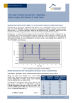
APPLICATION NOTE 409
Using TCM 310 transceivers in bidirectional low power applications
EnOcean TCM 310 device default firmware is called “GatewayController” and it uses the ESP3
communication protocol.
Typical applications are line powered, working as receiver/transceiver which “never sleeps”
therefore consuming > 33 mA@3 V (receiver on) continuously.
One of TCM 310 less known, because actually typical unused features for a transceiver is
that it has a watchdog and it can be put in “deep sleep” (energy saving mode) through correspondingly ESP3 serial common command “CO_WR_SLEEP” (for x milliseconds time period) as shown below:
The device deep sleep current drops then below 0.3 µA (meaning factor about > 100k less
vs. “normal mode”).
An issue is that in deep sleep the device can’t neither receive nor transmit any messages,
neither over its radio nor over its serial interface. The only possibility to wake-up from deep
sleep remains its watchdog or a SOR (= Supply-On Reset).
The proposed circuit shows just one implementation example of this feature on a TCM 310
device used as transceiver in some specific bidirectional low power applications.
An energy balance respectively specific use case trade-off should be made however before
between two approaches:
a. switching TCM supply voltage off between two communication cycles (no deep sleep
current at all but relatively long, up to 500 milliseconds according user manual) “cold”
start-up time by (same) high current, vs.:
b. keeping it instead in deep sleep mode by significantly faster start-up (few milliseconds), depending on the required communication frequency.
© EnOcean | www.enocean.com
Subject to modifications | Christian Bach | Jun. 2015 | Page 1/ 4
APPLICATION NOTE 409
Using TCM 310 transceivers in bidirectional low power applications
In some low power applications like i.e. wireless heating valve actuators the device could be
operated most of the time in deep sleep waking up only cyclical and for very short time
frames to communicate with the system (i.e. an ultralow power controller). In this way high
amounts of energy can be saved, enabling the device to work powered i.e. by battery or
even energy harvester.
The example below shows how to cut the UART lines of the EnOcean Dolphin based device
during deep sleep in low power applications in order to avoid reverse residual currents and
minimize accordingly the system current consumption. Typical use cases are applications
where a third part ultralow power microcontroller used as “master” cyclical communicates
through UART with TCM 310. The ultralow power master drives i.e. a heating valve (actuator) and is usually always “on”. It communicates serial over very short time frames through
the UART (ESP3 protocol) with the TCM device (slave). The device has an internal watchdog
and sleeps most time. The master is waiting then on TCM 310 wakeup (readiness), confirmed by the ESP3 “CO_READY” message, communicates with (for milliseconds) and finally
sends a new ESP3 “CO_WR_SLEEP” (for a determined time, see above) command on UART
to the device. This automatically confirms the received ESP3 command (RET_OK) and goes
sleep for the given time, wakes up then again and a new communication cycle starts.
In the proposed circuit T1 and Q1 are driven by DVDD to switch IOVDD (supply voltage for
all I/O’s) to VDD on during the communication and off thereafter. The UART “cutting” circuit
is identical for both I/O lines and consists of N-channel enhancement MOSFET’s (Q2, Q3)
driven by the DVDD/IOVDD.
Both MOSFET gates have to be connected direct to IOVDD, their sources to the correspondingly I/O lines on the slave (A) section side while their drains (D) to the same I/O lines on
the master (B) section side (always powered, common supply voltage VDD).
Note: most MOSFET have the substrate internally already connected to the source; otherwise
this should be done externally. The associate diodes between drain (D) and substrate
(source, S) present as intrinsic n-p junction of drain and substrate inside these MOSFET’s
play a key role in this circuit as shown below.
For the operation four states has to be considered:
1.
Device A (TCM, slave) sleeps,
DVDD is 0 V, T1 & Q1 are blocked
and the IOVDD path is consequently not supplied by +3.3 V
(VDD). Accordingly the I/O of the
slave section is in “three-state”.
The gate and the source of the
MOSFET are both “three-state”,
so their VGS are below the threshold voltage and both MOSFET are
not conducting. This allows that
the UART lines at the master section are i.e. pulled up by their
own pull-up (internal) resistors to
+3.3 V. The consequently invers
biased (integrated) MOSFET diodes are blocking however both
I/O lines which are consequently
physically “interrupted” between
TCM (A, slave) and B (master).
© EnOcean | www.enocean.com
Subject to modifications | Christian Bach | Jun. 2015 | Page 2/ 4
APPLICATION NOTE 409
Using TCM 310 transceivers in bidirectional low power applications
2.
Device A (slave) wakes up (internal watchdog), IOVDD is switched through T1 & Q1 on
(to VDD = +3.3 V), consequently its I/O lines are internally pulled up (default). As long
as no device actively communicates (pulling down the correspondingly I/O side) they
remain HIGH: the gate and the source of the MOSFET are both at +3.3 V (device A), so
the VGS is below the threshold voltage and the MOSFET’s are not conducting (internal
diodes also not because having on both side HIGH level). This allows that the correspondingly I/O lines on the master section (B) side are pulled up by its own (internal)
pull-up resistors to the same +3.3 V. The I/O lines of both sections stay HIGH.
3.
Now device A (slave) sends i.e. a message to the device B (master) through I/O, means
temporary pulls i.e. down the correspondingly I/O line to LOW. The source of the correspondingly MOSFET becomes also LOW, while the gate stay at +3.3 V (IOVDD). The VGS
rises above the threshold and the MOSFET becomes conducting. Now the same line on
the master section side is also (temporary) pulled down to LOW by the device A via the
conducting MOSFET. The correspondingly I/O line on both sections becomes LOW.
4.
Same situation but now device B (master) pulls (temporary) down the correspondingly
I/O line to LOW (by sending i.e. a “go sleep” message to the slave). Via the now direct
biased drain-substrate diode of the MOSFET the slave section is in first instance pulled
(temporary) down until VGS passes the threshold and the MOSFET becomes conducting.
Now the I/O line of the slave section is further pulled down to LOW by the B device via
the conducting MOSFET. The correspondingly I/O line on both sections becomes LOW.
Conclusion: the above described states show that the logic levels are correctly transferred
in both directions of the UART, independent who is the driving section (A or B). It also shows
that during sleep the UART lines between slave and master are cut so no residual currents
flow from VDD over the TCM I/O’s in this time. The circuit complies with the Dolphin Core
requirements regarding GPIO supply voltage in deep sleep mode and minimizes accordingly
the current consumption of the system.
Note: for correct operation the supply voltage VDD (and IOVDD) should be common (i.e.
+3.3 V) for both devices, master and slave. With a VGS threshold voltage of about 1 V below
the lowest VDD the circuit will operate properly. If for example the lowest VDD is +3 V, a
threshold voltage VGS of maximum 2 V is therefore allowed. Discrete BSS138 (N-channel Enhancement Mode) respectively BSS84 (P-channel Enhancement Mode) small signal SMD
MOSFET’s, both with low VGS are a good choice therefore. R1, R2 and R3 can be very large,
typically merely MΩ, up to tens of MΩ.
The screen shot picture shows the above described
behavior. Signals color: green DVDD, pink IOVDD,
yellow and blue the two UART lines (I/O’s).
From left to right: both device are initially awaken,
TCM device receives (on ADIO6, yellow) the command “Go sleep” from the master. It confirms immediately the received command (ADIO7, blue) to
master and then it goes sleep (DVDD, green fails
to Low), followed with some delay by IOVDD
(pink) and UART (yellow & blue). While the master
(B) is still on, the TCM UART paths (ADIO6 and
ADIO7) are “open” during TCM sleep time (right in
picture).
© EnOcean | www.enocean.com
Subject to modifications | Christian Bach | Jun. 2015 | Page 3/ 4
APPLICATION NOTE 409
Using TCM 310 transceivers in bidirectional low power applications
Remark: Current TCM 310 FW are meantime optimized with regard to energy consumption; other as by formerly TCM 310 FW versions, starting with version “GATEWAYCTRL
2.11.0.8” (TCM 310 FW release -14 and higher), the receiver (highest current consumption)
will be switched off immediately after receiving the command “CO_WR_SLEEP”, enabling
additional energy savings.
Further Documentation:
https://www.enocean.com/de/enocean_module/tcm-310/
https://www.enocean.com/esp
https://www.enocean.com/dolphin-core-description/
https://www.enocean.com/fileadmin/redaktion/pdf/app_notes/AN101_POWER_SUPPLY_LAY
OUT_2015.pdf
Disclaimer
The information provided in this document describes typical features of the EnOcean radio system and should not
be misunderstood as specified operating characteristics. No liability is assumed for errors and / or omissions. We
reserve the right to make changes without prior notice. For the latest documentation visit the EnOcean website at
www.enocean.com.
© EnOcean | www.enocean.com
Subject to modifications | Christian Bach | Jun. 2015 | Page 4/ 4