1
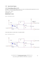
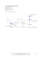
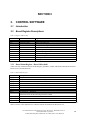
PCIe-OPTO16x16
User’s Manual
16 Input Bits
16 Output Bits
Opto-Isolator Board
General Standards Corporation
8302A Whitesburg Drive
Huntsville, AL 35802
Phone: (256) 880-8787
Fax: (256) 880-8788
URL: www.generalstandards.com
E-mail: [email protected]
User Manual for the PCIe-OPTO16x16 Card, Revision: A, Manual Revision: B
General Standards Corporation
8302A Whitesburg Drive Huntsville, AL 35802, Phone: (256) 880-8787
1
User Manual for the PCIe-OPTO16x16 Card, Revision: A, Manual Revision: B
General Standards Corporation
8302A Whitesburg Drive Huntsville, AL 35802, Phone: (256) 880-8787
2
PREFACE
General Standards Corporation
Copyright (C) 2011 General Standards Corp.
Additional copies of this manual or other literature may be obtained from:
General Standards Corporation
8302A Whitesburg Dr.
Huntsville, Alabama 35802
Tele: (256) 880-8787
FAX: (256) 880-8788
E-mail: [email protected]
The information in this document is subject to change without notice.
General Standards Corp. makes no warranty of any kind with regard to this material, including, but not
limited to, the implied warranties of merchantability and fitness for a particular purpose. Although
extensive editing and reviews are performed before release to ECO control, General Standards Corp.
assumes no responsibility for any errors that may exist in this document. No commitment is made to update
or keep current the information contained in this document.
General Standards Corp. does not assume any liability arising out of the application or use of any product
or circuit described herein, nor is any license conveyed under any patent rights or any rights of others.
General Standards Corp. assumes no responsibility for any consequences resulting from omissions or
errors in this manual, or from the use of information contained herein.
General Standards Corp. reserves the right to make any changes, without notice, to this product to
improve reliability, performance, function, or design.
All rights reserved
No part of this document may be copied or reproduced in any form or by any means without prior written
consent of General Standards Corp.
This user’s manual provides information on the specifications, theory of operation, register level
programming, installation of the board and information required for customized hardware/software
development.
User Manual for the PCIe-OPTO16x16 Card, Revision: A, Manual Revision: B
General Standards Corporation
8302A Whitesburg Drive Huntsville, AL 35802, Phone: (256) 880-8787
3
RELATED PUBLICATIONS
The following manuals and specifications provide the necessary information for in depth understanding of
the specialized parts used on this board.
EIA Standard for the RS-422A Interface (EIA order number EIA-RS-422A)
PCI Local Bus Specification Revision 2.1 June 1, 1995. Questions regarding the PCI specification be
forwarded to:
PCI Special Interest Group
P.O. Box 14070
Portland, OR 97214
(800) 433- 5177 (U.S.)
(503) 797-4207 (International)
(503) 234-6762 (FAX)
User Manual for the PCIe-OPTO16x16 Card, Revision: A, Manual Revision: B
General Standards Corporation
8302A Whitesburg Drive Huntsville, AL 35802, Phone: (256) 880-8787
4
PCIe-OPTO16x16 Documentation History
1.
Alterations for PCIe-OPTO16x16 Board Assembly.
2.
2010-09-15
Added PCI Sub-System Identifier.
Section 3.2.1 Added Firmware Revision Identifiers.
Finished adding Mailbox Information.
3. 2011-02-07 – Rev A
Re-Wrote PLX EEPROM section.
Added Full PLX EEPROM as an Appendix.
Manually added the Appendix's into the Table of Contents .
Added / Explained how the PEX8311AA works.
Updated Layout Picture to Rev A.
Added Test Register 1 and 2
Changed Register bit level descriptions. Tried to Clarify descriptions.
Added Register Contents tables for all registers.
Added Note, Schmidt Trigger Input has been removed.
Fix descriptions for COS Byte Clears.
Fixed “Differences from OPTO32” - Introduction, Input's and Outputs were mixed up.
4. 2011-02-08 – Rev B
Changes Per Don
Revision History is on this page.
Period missing on page 11
Period missing on page 13
Fixed COS Polarity Type.
Fixed Initialization Punctuation.
Fixed Class code description.
Fixed Typo in Interrupt Appendix, test for if this board generated Interrupt.
Made Page Numbers Consistent.
User Manual for the PCIe-OPTO16x16 Card, Revision: A, Manual Revision: B
General Standards Corporation
8302A Whitesburg Drive Huntsville, AL 35802, Phone: (256) 880-8787
5
User Manual for the PCIe-OPTO16x16 Card, Revision: A, Manual Revision: B
General Standards Corporation
8302A Whitesburg Drive Huntsville, AL 35802, Phone: (256) 880-8787
6
Table Of Contents
1. Introduction..............................................................................................................................11
1.1 Differences From OPTO32 Family...............................................................................................11
1.2 Card Features ................................................................................................................................12
2. INSTALLATION AND MAINTENANCE..............................................................................13
2.1 Card Configuration........................................................................................................................13
2.2 Installation......................................................................................................................................13
2.2.1 Physical Installation.....................................................................................................................................13
2.2.2 Input / Output Cable Connectors..................................................................................................................14
2.3 System Configuration....................................................................................................................15
2.3.1 Opto-Isolated Inputs.....................................................................................................................................15
2.3.2 Opto-Isolated Outputs..................................................................................................................................17
3. CONTROL SOFTWARE.........................................................................................................19
3.1 Introduction....................................................................................................................................19
3.2 Board Register Descriptions..........................................................................................................19
3.2.1 Board Status Register - Board Offset 0x00..................................................................................................19
3.2.2 Board Control Register - Board Offset 0x00 -.............................................................................................20
3.2.3 Received Data Register - Board Offset 0x04 ..............................................................................................20
3.2.4 Change of State Register - Board Offset 0x08.............................................................................................21
3.2.5 Receive Event Counter - Board Offset 0x0c................................................................................................21
3.2.6 COS Interrupt Enable Register - Board Offset 0x010.................................................................................21
3.2.7 COS Polarity Register - Board Offset 0x014...............................................................................................22
3.2.8 Clock Division Register - Board Offset 0x018............................................................................................22
3.2.9 Output Data Register - Board Offset 0x01c.................................................................................................23
3.2.10 Test Register 1...........................................................................................................................................23
3.2.11 Test Register 2...........................................................................................................................................23
4. PEX 8311 Notes .......................................................................................................................24
4.1 Initialization...................................................................................................................................24
4.1.1 Device ID / Vendor ID.................................................................................................................................24
4.1.2 Sub-System ID / Vendor ID.........................................................................................................................25
4.1.3 Class Code / Revision .................................................................................................................................25
4.1.4 Mailbox 0 ....................................................................................................................................................25
4.1.5 Mailbox 1 ....................................................................................................................................................25
4.1.6 Address Space 0 Range PCI to Local .........................................................................................................26
4.1.7 Address Space 0 Base Address (Remap) ....................................................................................................26
Appendix A : Interrupts............................................................................................................................................27
Appendix B : PLX EEPROM Contents...................................................................................................................29
User Manual for the PCIe-OPTO16x16 Card, Revision: A, Manual Revision: B
General Standards Corporation
8302A Whitesburg Drive Huntsville, AL 35802, Phone: (256) 880-8787
7
Table Of Figures
Figure 1 Board Layout.................................................................................................................13
Figure 2 Input Channels 0-15, Typical.......................................................................................16
Figure 3 Normal Outputs, Bits 0-3..............................................................................................17
Figure 4 Normal Outputs, Bits 8-15............................................................................................17
Figure 5 Diode Clamped Outputs, Bits 4-7.................................................................................18
User Manual for the PCIe-OPTO16x16 Card, Revision: A, Manual Revision: B
General Standards Corporation
8302A Whitesburg Drive Huntsville, AL 35802, Phone: (256) 880-8787
8
Table Of Tables
Table 2-1 Input / Output Cable Pin Assignments.......................................................................14
Table 2-2 Input Channels Bias Resistors Locations..................................................................15
Table 2-3 Input Channels Bias Resistor Values.........................................................................15
Table 3-4 Register Address Map..................................................................................................19
Table 3-5 Board Status Register..................................................................................................19
Table 3-6 Board Control Register...............................................................................................20
Table 3-7 Received Data Register................................................................................................20
Table 3-8 Change of State register..............................................................................................21
Table 3-9 Receive Event Counter................................................................................................21
Table 3-10 COS Interrupt Enable Register.................................................................................21
Table 3-11 COS Polarity Register...............................................................................................22
Table 3-12 Clock Division Register.............................................................................................22
Table 3-13 Output Data Register.................................................................................................23
Table 3-14 Test Register 1...........................................................................................................23
Table 3-15 Test Register 2...........................................................................................................23
Table 4-16 EEPROM Register Initialization..............................................................................24
Table 4-17 Device ID / Vendor ID Register Description............................................................24
Table 4-18 Sub-System ID and Vendor ID Register Description..............................................25
Table 4-19 Class Code / Revision Register..................................................................................25
Table 4-20 Mailbox 0...................................................................................................................25
Table 4-21 Mailbox 1...................................................................................................................25
Table 4-22 Space 0 Range PCI to Local.....................................................................................26
Table 4-23 Address Space 0 Base Address (Remap)...................................................................26
Table B-24 PLX EEPROM Contents..........................................................................................29
User Manual for the PCIe-OPTO16x16 Card, Revision: A, Manual Revision: B
General Standards Corporation
8302A Whitesburg Drive Huntsville, AL 35802, Phone: (256) 880-8787
9
User Manual for the PCIe-OPTO16x16 Card, Revision: A, Manual Revision: B
General Standards Corporation
8302A Whitesburg Drive Huntsville, AL 35802, Phone: (256) 880-8787
10
SECTION 1
1.
Introduction
The PCIe-OPTO16x16 board is a high performance Single Lane PCI Express card offering 16 Opto-Isolated inputs
and 16 Opto-Isolated outputs.
1.1
Differences From OPTO32 Family
The PCIe-OPTO16x16 is based on the OPTO32 family. It was designed to provide a migration path from the
OPTO32 family to the OPTO16 on the PCIe Bus.
The following differences exist between the OPTO32 and the PCIe-OPTO16x16.
•
Output Bits 0-7 are the same as the OPTO32 Family.
•
Input Bits 0-15 are the same as the OPTO32 Family.
•
Input Bits 16-23 have been removed.
•
Output Bits 8-15 were placed where OPTO32 Input 16-23 were at.
•
Special Schmidt Trigger Input has been removed. All Inputs are the same.
•
True PCIe Form factor.
User Manual for the PCIe-OPTO16x16 Card, Revision: A, Manual Revision: B
General Standards Corporation
8302A Whitesburg Drive Huntsville, AL 35802, Phone: (256) 880-8787
11
1.2
Card Features
• 16 optically isolated inputs
•
Selectable input voltage range thru use of field replaceable bias resistors.
•
Industry Standard 8 Pin Sip Resistors – 770-83-Rxx Series.
• 16 optically isolated outputs - 12 normal, 4 Diode Clamped
• Software Programmable clock debounce rate
• Software Programmable Change of State detection. Rising edge or falling edge per input channel
• Software Programmable Interrupts on any or all Change of State bit(s)
• Software Pre-loadable Event counter on Input Bit 15
• Programmable Interrupt on Event Counter Overflow
• Built in Self-Test Features.
•
Registers are Read / Write.
•
Ability to monitor the Debounce Clock.
The board uses the PEX 8311 PCIe single lane interface chip to provide the advanced features of the PCIe interface
environment. These features include:
• Programmable Little Endian / Big Endian swapping
• PCIe cycles Asynchronous to local bus cycles
• Software Programmable board base address
User Manual for the PCIe-OPTO16x16 Card, Revision: A, Manual Revision: B
General Standards Corporation
8302A Whitesburg Drive Huntsville, AL 35802, Phone: (256) 880-8787
12
SECTION 2
2.
INSTALLATION AND MAINTENANCE
2.1
Card Configuration
Figure 1 Board Layout
2.2
Installation
2.2.1
Physical Installation
Selectable input voltage range thru use of field replaceable bias resistors using standard 8 pin SIP isolation resistors.
These bias resistor packages are socketed for easy replacement. One bias resistor package will affect the input
channels on nibble boundaries.
User Manual for the PCIe-OPTO16x16 Card, Revision: A, Manual Revision: B
General Standards Corporation
8302A Whitesburg Drive Huntsville, AL 35802, Phone: (256) 880-8787
13
2.2.2
Input / Output Cable Connectors
Table 2-1 Input / Output Cable Pin Assignments
PIN NUMBER
1
2
3
4
5
6
7
8
9
10
11
12
13
14
15
16
17
18
19
20
21
22
23
24
25
26
27
28
29
30
31
32
33
34
SIGNAL
IN CH00 HI
IN CH00 LO
IN CH01 HI
IN CH01 LO
IN CH02 HI
IN CH02 LO
IN CH03 HI
IN CH03 LO
IN CH04 HI
IN CH04 LO
IN CH05 HI
IN CH05 LO
IN CH06 HI
IN CH06 LO
IN CH07 HI
IN CH07 LO
IN CH08 HI
IN CH08 LO
IN CH09 HI
IN CH09 LO
IN CH10 HI
IN CH10 LO
IN CH11 HI
IN CH11 LO
IN CH12 HI
IN CH12 LO
IN CH13 HI
IN CH13 LO
IN CH14 HI
IN CH14 LO
IN CH15 HI
IN CH15 LO
LOG OUT CH8 HI
LOG OUT CH8 LO
PIN NUMBER
35
36
37
38
39
40
41
42
43
44
45
46
47
48
49
50
51
52
53
54
55
56
57
58
59
60
61
62
63
64
65
66
67
68
SIGNAL
LOG OUT CH9 HI
LOG OUT CH9 LO
LOG OUT CH10 HI
LOG OUT CH10 LO
LOG OUT CH11 HI
LOG OUT CH11 LO
LOG OUT CH12 HI
LOG OUT CH12 LO
LOG OUT CH13 HI
LOG OUT CH13 LO
LOG OUT CH14 HI
LOG OUT CH14 LO
LOG OUT CH15 HI
LOG OUT CH15 LO
LOG OUT CH0 HI
LOG OUT CH0 LO
LOG OUT CH1 HI
LOG OUT CH1 LO
LOG OUT CH2 HI
LOG OUT CH2 LO
LOG OUT CH3 HI
LOG OUT CH3 LO
PWR OUT CH4 HI
PWR OUT CH4 LO
PWR OUT CLAMP 4
PWR OUT CH5 HI
PWR OUT CH5 LO
PWR OUT CLAMP 5
PWR OUT CLAMP 6
PWR OUT CH6 HI
PWR OUT CH6 LO
PWR OUT CLAMP 7
PWR OUT CH7 HI
PWR OUT CH7 LO
User Manual for the PCIe-OPTO16x16 Card, Revision: A, Manual Revision: B
General Standards Corporation
8302A Whitesburg Drive Huntsville, AL 35802, Phone: (256) 880-8787
14
2.3
System Configuration
2.3.1
Opto-Isolated Inputs
Selectable input voltage range thru use of field replaceable bias resistors, labeled RIN, using standard 8 pin SIP
isolation resistors. These bias resistor packages are socketed for easy replacement One bias resistor package will
affect the input channels on nibble boundaries as follows:
Table 2-2 Input Channels Bias Resistors Locations.
Resistor Location
R10
R9
R8
R2
Input Channels
IN CH00 thru IN CH03
IN CH04 thru IN CH07
IN CH08 thru IN CH11
IN CH12 thru IN CH15
Current Limiting Resistor Values should be chosen to provide a Minimum input current of 2.3 mA. Typical resistor
values for input voltage levels are as follows:
Table 2-3 Input Channels Bias Resistor Values
Input Voltage Range
5V
12 V
28 V
48 V
Bias Resistor Values
2200 ohms
5100 ohms
12000 ohms
20000 ohms
User Manual for the PCIe-OPTO16x16 Card, Revision: A, Manual Revision: B
General Standards Corporation
8302A Whitesburg Drive Huntsville, AL 35802, Phone: (256) 880-8787
15
2.3.1.1 Input Channels 0-15
Isolation Voltage – 5000 V
Current Transfer Ratio – 80-600%
Min Input Current – 2.3 mA.
Max Input Current – 80 mA.
Typical Ton/Toff – 3/5 uSec.
Figure 2 Input Channels 0-15, Typical
User Manual for the PCIe-OPTO16x16 Card, Revision: A, Manual Revision: B
General Standards Corporation
8302A Whitesburg Drive Huntsville, AL 35802, Phone: (256) 880-8787
16
2.3.2
Opto-Isolated Outputs
2.3.2.1 Normal Outputs Bits 0-3, 8-15
Output Bits 0-3 contain an Optional Pullup resistor to VCC that is not normally installed. Output Bits 8-15 are the
same as bits 0-3 except the optional resistor does not exist.
Isolation Voltage – 5000 V
VCEO (Max) – 60 V
Maximum Current – 100 ma.
Typical Ton/Toff – 3/5 uSec.
Figure 3 Normal Outputs, Bits 0-3
100 K isolation Resistor is Optional and is not normally installed.
Figure 4 Normal Outputs, Bits 8-15
User Manual for the PCIe-OPTO16x16 Card, Revision: A, Manual Revision: B
General Standards Corporation
8302A Whitesburg Drive Huntsville, AL 35802, Phone: (256) 880-8787
17
2.3.2.2 Diode Clamped Outputs Bits 4-7
Isolation Voltage – 5000 V
VCEO (Max) – 60 V
Maximum Current – 100 ma.
Typical Ton/Toff – 3/5 uSec.
Figure 5 Diode Clamped Outputs, Bits 4-7
User Manual for the PCIe-OPTO16x16 Card, Revision: A, Manual Revision: B
General Standards Corporation
8302A Whitesburg Drive Huntsville, AL 35802, Phone: (256) 880-8787
18
SECTION 3
3.
CONTROL SOFTWARE
3.1
Introduction
3.2
Board Register Descriptions
Table 3-4 Register Address Map
Board Offset
0x00
0x00
0x04
0x08
0x0c
0x010
0x014
0x018
0x01c
0x020
0x024
3.2.1
Size
32 Bits Read Only
8 Bits Write Only
16 bits Read ONLY
16 bits Read / Write
16 bits Read / Write
16 bits Read / Write
16 bits Read / Write
24 bits Read / Write
16 bits Read / Write
32 Bits Read / Write
32 Bits Read / Write
Register Name
Board Status Register
Board Control Register
Received Data Register
Change of State Register
Receive Event Counter
COS Interrupt Enable Register
COS Polarity Register
Clock Division Register
Output Data Register
Test Register 1
Test Register 2
Board Status Register - Board Offset 0x00
32 Bits read only. With Firmware Rev B this Register expanded to 32 Bits with Fields to Identify the Firmware
Revision Level, and the Board ID.
Table 3-5 Board Status Register
Field
Bit[0]
Bit[1]
Bit[2]
Bit[3]
Bit[4]
Bit[5]
Bit[6]
Bit[7]
Description
Int Byte LO Out H = bits 7 - 0 COS interrupt status
Int Byte MD Out H = bits 15 - 8 COS interrupt status
Reserved
Rx Event Overflow H = Event Overflow status
Master Int Out = Master Interrupt Status – 1=Interrupt into the PLX
Slow Debounce Clock ;
Enable Rx Event Overflow H = Interrupt Enable for Event Overflow Read Back
Fail LED ON L – Read Back
Prior to Firmware Rev B, Bits 8..31 were not used and Undefined.
With Firmware Rev B the Following Fields were added.
Bit[15..8]
Reserved – Set to 0x00.
Bit[23..16]
Current Firmware Rev Level - was added with Rev B – Set to 0x01 for Rev B.
Bit[31..24]
Board Identifier. Set to 0x01 to Identify the OPTO16x16 Board Family.
When the FW Rev field was added it was set to 0x01because it was the first time the Field was Present. If there is a
future revision it will be adjusted to be consistent with the Actual Firmware Revision Level.
User Manual for the PCIe-OPTO16x16 Card, Revision: A, Manual Revision: B
General Standards Corporation
8302A Whitesburg Drive Huntsville, AL 35802, Phone: (256) 880-8787
19
3.2.2
Board Control Register - Board Offset 0x00 -
8 Bits write only. Table 3-6 Board Control Register
Field
Bit[0]
Bit[1]
Bit[2]
Bit[3]
Bit[4]
Bit[5]
Bit [6]
Bit [7]
Description
Clear Int Byte LO H = clear COS bits 7 - 0
Clear Int Byte MD H = clear COS bits 15 - 8
Reserved
Clear Rx Event Overflow H =Clear Event Counter Overflow Status
Master Clear = - Clear All COS bits and Event Counter Overflow Status bit.
Reserved
Enable Rx Event Overflow H - 1 = Interrupt enable.
Fail LED ON L - 0=LED On / 1 = LED Off
NOTE: Bits 0-4 are self-clearing pulses that are written as a 1 to clear the interrupt source. The
bits will then self clear so that another host operation is not required.
NOTE: The Clear COS Bytes, or the Master Clear (bit[4]), will clear ANY COS register bit that is
set regardless of the bits Interrupt Enable Status. For Individual COS bit clearing, Write a 1 to
the COS bit you wish to clear.
Event Overflow status will only be cleared by Clear Event Overflow or by Master Clear, Bit[4]. Loading the
Event Counter WILL NOT clear out the event overflow status.
3.2.3
Received Data Register - Board Offset 0x04
16 bits. Debounced Receive data bits 0 - 16. Read ONLY.
The Input Data Bits, After they have been Debounced
Table 3-7 Received Data Register
Field
15:0
31:16
Description
Debounced Receive Data bits 0 - 16. Read ONLY The Debounced Input Data Bits.
Reserved – Undefined
User Manual for the PCIe-OPTO16x16 Card, Revision: A, Manual Revision: B
General Standards Corporation
8302A Whitesburg Drive Huntsville, AL 35802, Phone: (256) 880-8787
20
3.2.4
Change of State Register - Board Offset 0x08
16 bits - Change of State Detected. Polarity programmed thru COS Polarity register, 0x014.
If a COS bit is set, then it will stay set until cleared by the host. A COS bit can be cleared by writing a 1 to a COS bit
that is set. Writing a zero will have no effect. Writing a 1to a bit that is 0 will do nothing. COS bits may also be
cleared by using the board control register Byte clears or using the board control master clear.
Table 3-8 Change of State register
Field
15:0
31:16
3.2.5
Description
Change of State Data bits 0 - 16. Writing a 1 will clear a bit that is set.
Reserved – Undefined
Receive Event Counter - Board Offset 0x0c
16 bits Read / Write. Reset to Zero.
This counter may be read at any time by the host. Counter will increment once for every Debounced Rising edge
detected on input data bit 15. When the counter is 0x0ffff and increments the Rx event overflow status bit will be set
and can be used to generate an interrupt.
Table 3-9 Receive Event Counter
Field
15:0
Description
Receive Event Counter
31:16
Reserved – Undefined
3.2.6
COS Interrupt Enable Register - Board Offset 0x010
16 bits. Read / Write. Reset to Zero.
Each bit will be bitwise ANDED with the COS register and all of the results OR’ed together to generate an Interrupt.
A 1 will enable the corresponding interrupt. A 0 will disable that bit from generating an interrupt.
Table 3-10 COS Interrupt Enable Register
Field
15:0
Description
COS Interrupt Enable Register 1=Enable Interrupt for that corresponding COS bit.
31:16
Reserved – Undefined
User Manual for the PCIe-OPTO16x16 Card, Revision: A, Manual Revision: B
General Standards Corporation
8302A Whitesburg Drive Huntsville, AL 35802, Phone: (256) 880-8787
21
3.2.7
COS Polarity Register - Board Offset 0x014
16 bits. Read / Write. Reset to Zero.
When the corresponding bit is zero, the COS detection for that bit will be set by a detected High to Low transition.
When Set to a 1 the COS detection for that bit will look for Low to High transitions. Reset to all zeros.
Table 3-11 COS Polarity Register
Field
15:0
Description
COS Polarity Register - 1=Low to Hi will set COS Bit. 0=Hi to Low will set COS, Per Bit. .
31:16
Reserved – Undefined
3.2.8
Clock Division Register - Board Offset 0x018
24 bits. Read / Write. Reset to Zero.
Table 3-12 Clock Division Register
Field
23:0
Description
Clock Division Register - Sets the Clock Division Rate.
31:24
Reserved – Undefined
NOTE >>>> when altering this register, disable all interrupts and expect unusual results in the
COS Detection register.
A 24 Bit clock divider is provided for programmable Debounce delays. The debounce circuit registers the incoming
data 3 times in a daisy chain. When ALL 3 registers are high, the incoming data is a high. When the debounced data
register contains a 1, then ALL three registers must contain zero for the debounced data to transition back to a zero.
The clock for these holding registers is programmable thru the clock divider.
The Basic clock of the board is 20 MHz, 50 Ns. The Basic Clock Counter will always divide by 4, 200 Ns. Values of
0x0000 or 0x0001 will not alter this. When the clock divider is loaded with a larger value then the clock division
will be (count * 2) + 2. The Total debounce time will be 3 X (clock division time).
For Example: for a 15ms. debounce time. Clock period should be 5ms.
5ms / 50 Ns = 100000. -2 = 99998.
99998 / 2 = 49999 = 0x0c34f Hex.
User Manual for the PCIe-OPTO16x16 Card, Revision: A, Manual Revision: B
General Standards Corporation
8302A Whitesburg Drive Huntsville, AL 35802, Phone: (256) 880-8787
22
3.2.9
Output Data Register - Board Offset 0x01c.
16 bits - Read / Write. Reset to Zero.
The 16 bit output data register. Reset to All Zero’s. Writing a 1 to a bit will make that opto output conductive and
current will flow from 'HI' to 'LO'. Writing a 0 will turn the opto off and the output will be Non -Conductive from
'HI' to 'LO'
Table 3-13 Output Data Register
Field
15:0
Description
Output Data Register - Controls the Opto-Isolated Outputs. .
31:16
Reserved – Undefined
3.2.10 Test Register 1
32 Bits – Read / Write. Reset to Zero.
32 bit Register does not do anything. It was added to test 8, 16, and 32 Bit Reads and Writes.
Table 3-14 Test Register 1
Field
31:0
Description
Test Register 1 - Can be used for anything.
3.2.11 Test Register 2
32 Bits – Read / Write. Reset to Zero.
32 bit Register does not do anything. It was added to test 8, 16, and 32 Bit Reads and Writes.
Table 3-15 Test Register 2
Field
31:0
Description
Test Register 2
- Can be used for anything.
User Manual for the PCIe-OPTO16x16 Card, Revision: A, Manual Revision: B
General Standards Corporation
8302A Whitesburg Drive Huntsville, AL 35802, Phone: (256) 880-8787
23
4.
PEX 8311 Notes
The PCIe-OPTO16x16 uses the PLX Technologies PEX8311AA Interface chip. In the System Devices list this chip
will show up as 2 devices, a 8311 PCIe to PCI bridge and a 9056 PCI to local bus adapter.
4.1
Initialization
When the PEX8311 is reset, the 9056 part of the chip will initialize itself from an on board serial EEPROM that is
programmed at General Standards. A brief description of some of the Registers follows.
Table 4-16 EEPROM Register Initialization
Eeprom Addr
0x00
0x44
0x04
0x0c
0x10
0x14
0x18
PCI Addr
0x00
0x2c
0x08
0x78
0x7c
Description
Device ID / Vendor ID
Sub-System ID / Vendor ID
Class Code / Revision
Mailbox 0
Mailbox 1
Space 0 range PCI to Local
Space 0 Base Address (remap)
Value After Reset
0x905610B5
0x346010b5
0x078000ba
0x00020002
0x00020100
0xffffff80
0x00000001
A list of the full EEPROM contents is located in Appendix B.
4.1.1
Device ID / Vendor ID
Device ID and Vendor ID are used to identify the PLX Device during configuration cycles.
Table 4-17 Device ID / Vendor ID Register Description
Field
15:0
31:16
Description
Vendor ID - Identifies the manufacturer of the device. Defaults to the PCI
SIG issued vendor ID of PLX
Device ID - Identifies the particular device. Defaults to the PLX part number
for PCI interface chip.
Value After Reset
0x10B5
0x9056
User Manual for the PCIe-OPTO16x16 Card, Revision: A, Manual Revision: B
General Standards Corporation
8302A Whitesburg Drive Huntsville, AL 35802, Phone: (256) 880-8787
24
4.1.2
Sub-System ID / Vendor ID
Sub-System ID and Vendor ID are used to identify the PCIe-OPTO16x16 during configuration cycles.
Table 4-18 Sub-System ID and Vendor ID Register Description
Field
15:0
31:16
4.1.3
Description
Vendor ID - Identifies the manufacturer of the device. Defaults to the PCI
SIG issued vendor ID of PLX.
Sub-System ID - Identifies the particular device. Sub-System ID Assigned to
the OPTO16x16 by PLX.
Value After Reset
0x10B5
0x3460
Class Code / Revision
When loaded from the EE Prom this register will identify the device Base Class Code, Sub-Class Code and Revision
of the PLX Device. PLX Revision is hard coded in the device.
Table 4-19 Class Code / Revision Register
Field
07:00
15:08
23:16
31:24
4.1.4
Description
Revision Level of the PLX – currently
Register Level Programming Interface - 0x00 - None Defined
Sub-Class Code - 0x80 – Other Communications Device
Base Class Code 0x07 – Simple Communications Controller
Value After Reset
0xba
0x00
0x08
0x07
Mailbox 0
When loaded from the EE Prom, this mailbox is used to contain values to identify the PLD revision, and EE Prom
Revision levels of this board.
Table 4-20 Mailbox 0
Field
15:0
31:16
4.1.5
Description
PLD Revision Level – Revision Level of the FPGA on the OPTO16x16.
Currently 0x02 = Rev B .
EE Prom Revision Level – Revision Level of the PLX EEPROM contents.
Currently 0x02 = Rev B .
Value After Reset
0x0002
0x0002
Mailbox 1
When loaded from the EE Prom, this mailbox register is used to identify the overall Board assembly level, and to
Identify this Assembly.
Table 4-21 Mailbox 1
Field
15:0
31:16
Description
Assembly Identifier –
0x0100 Identifies the OPTO16x16
Board Assembly Revision Level
Currently 0x02 = Rev B .
Value After Reset
0x0100
0x0002
User Manual for the PCIe-OPTO16x16 Card, Revision: A, Manual Revision: B
General Standards Corporation
8302A Whitesburg Drive Huntsville, AL 35802, Phone: (256) 880-8787
25
4.1.6
Address Space 0 Range PCI to Local
Size of the Address Space required for the OPTO16x16. The OPTO16x16 uses 128 Bytes of Memory Space.
Table 4-22 Space 0 Range PCI to Local
Field
31:00
4.1.7
Description
Address Space 0 Range – Zero's indicate the size in Bytes of the Address
Space to be reserved for the Board.
Bit 0 Indicates the Board is mapped into Memory Space.
The OPTO16x16 uses 128 Bytes of Memory Space.
Value After Reset
0xffffff80
Address Space 0 Base Address (Remap)
There is no address space Remap for the Board. Bit Zero indicates that Address Space 0 is Active for writing to
Local Registers on the Board.
Table 4-23 Address Space 0 Base Address (Remap)
Field
31:00
Description
Address Space 0 Base Address (Remap) 0x01
Bit 0 Indicates that Address Space 0 is Active.
Value After Reset
0x00000001
User Manual for the PCIe-OPTO16x16 Card, Revision: A, Manual Revision: B
General Standards Corporation
8302A Whitesburg Drive Huntsville, AL 35802, Phone: (256) 880-8787
26
Appendix A
INTERRUPTS:
For Interrupt Operation, the Desired Interrupts are Enabled on the Opto isolator board AND Interrupts MUST be
enabled At / Thru the PLX Interface chip. To enable Event Counter Overflow Interrupts, Bit[6] of the Board Control
Register must be set to a 1.
outportb(Opto_register_base_address + 0x00, 0xc0 );
// Byte write, Turn LED off, Enable Event Overflow Interrupt.
outportl(Opto_register_base_address + 0x0c, 0x0fffe );
// Long word write, Event Counter, -2.
// The Second Rising Edge detected will generate the Interrupt
To Enable COS Interrupts, Any / All Desired COS Interrupt bit’s are enabled thru the COS Interrupt Enable
Register.
outportl(Opto_register_base_address + 0x010, 0x08421 ) ;
// Long word write, Offset 0x010, Enable Interrupts on
// COS Bit’s 0, 5, 10, and 15.
All other Machine dependent actions should be taken before the final steps in the process. Make ABSOLUTELY
sure that there is NO Pending status laying around that is already setting an interrupt action. Either use the master
clear’s
outportb(Opto_register_base_address + 0x00, 0xdf );
// Byte write, Turn LED off, Enable Event Overflow Interrupt.
// Master Clear All COS and Clear the Event Counter overflow .
// NOTE NOTE NOTE NOTE
// The Master Clear will Clear ALL COS Bits.
// The Byte Clear’s will ALSO Clear ALL COS Bits in that Byte.
// To Only Clear the Bit generating the Interrupt,
// you must use the individual Clear’s as
// Described below.
Or, Individual Clears for the COS and Event Overflow.
Outportl(Opto_register_base_address + 0x08, 0x08421 ) ;
// Long word write, Offset 0x08, COS register, Clear
// COS Bit’s 0, 5, 10, and 15. If they are set.
Outportb(Opto_register_base_address + 0x00, 0xc8 );
// Byte write, Turn LED off, Enable Event Overflow Interrupt.
// Clear Event Overflow
The final step is the write to the PLX interface that will enable it to generate Interrupts onto the PCI bus.
Outportl(PLX_io_base_address + 0x068, 0x00900 );
// Long word write, PLX interrupt control register,
// Bit’s 8 and 11, Enable Local input to generate PCI interrupts
User Manual for the PCIe-OPTO16x16 Card, Revision: A, Manual Revision: B
General Standards Corporation
8302A Whitesburg Drive Huntsville, AL 35802, Phone: (256) 880-8787
27
In the Interrupt Handler, there is NO action required to / with the PLX Interface chip. The only requirement to
remove the Asserted interrupt is to remove the Local source of the interrupt. Which would be the COS bit or the
event overflow.
temp = inportb(Opto_register_base_address + 0x00 ) ;
// Read the OPTO Board Status register
if ( (temp & 0x010) == 0x010 )
{
// Master Interrupt bit will be set in the Board Status
// Register if this board generated the Interrupt.
// Status Bits 0 thru 3 could also be examined to
// Determine Which Byte generated the Interrupt
// Or if the Event Counter Overflow generated
// The Interrupt.
.
.
.
.
// Finished processing, Now It’s time to clear the
// Pending Interrupt.
Outportl(Opto_register_base_address + 0x08, 0x08421 ) ;
// Long word write, Offset 0x08, COS register, Clear
// COS Bit’s 0, 5, 10, and 15. If they are set.
Outportb(Opto_register_base_address + 0x00, 0xc8 );
// Byte write, Turn LED off, Enable Event Overflow Interrupt.
// Clear Event Overflow
}
To Disable All Interrupt’s From the OPTO board, write to the PLX interface Chip.
Outportl(PLX_io_base_address + 0x068, 0x0000 );
// Long word write, PLX interrupt control register,
// Clear Bit’s 8 and 11, disable All PCI interrupts
User Manual for the PCIe-OPTO16x16 Card, Revision: A, Manual Revision: B
General Standards Corporation
8302A Whitesburg Drive Huntsville, AL 35802, Phone: (256) 880-8787
28
Appendix B
PLX EEPROM Contents:
The Full contents of the OPTO16x16 EEPROM for the 9056 portion of the interface chip are as follows.
Table B- 24 PLX EEPROM Contents
Eeprom
Addr
0x00
0x04
0x08
0x0c
0x10
0x14
0x18
0x1c
0x20
0x24
0x28
0x2c
0x30
0x34
0x38
0x3c
0x40
0x44
0x48
0x4c
0x50
0x54
0x58
0x5c
0x60
Description
Value After Reset
Device ID / Vendor ID
Class Code / Revision
Max / Min Latency / Int. Pin / Int. Line Routing Value
Mailbox 0
Mailbox 1
Space 0 range PCI to Local
Space 0 Base Address (remap)
Mode / DMA Arbitration register
VPD Boundary -Big / Little Endian descriptor
Expansion ROM Range – Not Used
Expansion ROM Re-Map – Not Used
Space 0 / Expansion ROM Descriptor
Direct Master to PCI Range – Not Used
Direct Master to PCI Local Base Address – Not Used
Direct Master to PCI IO/CFG Base Address -Not Used
Direct Master to PCI Memory Re-Map – Not Used
Direct Master to PCI IO/CFG PCI – Not Used
Sub-System ID / Vendor ID
Space 1 range PCI to Local – Not Used
Space 1 Base Address (remap) – Not Used
Space 1 Descriptor – Not Used
Hot Swap Control
PCI Arbiter Control
PM Capabilities
PM Control / Status
0x905610B5
0x07800002
0x00000100
0x00020002
0x00020100
0xffffff80
0x00000001
0x01200000
0x00300500
0x00000000
0x00000000
0x42000140
0x00000000
0x00000000
0x00000000
0x00000000
0x00000000
0x346010b5
0x00000000
0x00000000
0x00000000
0x00004c06
0x00000000
0x00024801
0x00000000
User Manual for the PCIe-OPTO16x16 Card, Revision: A, Manual Revision: B
General Standards Corporation
8302A Whitesburg Drive Huntsville, AL 35802, Phone: (256) 880-8787
29