1
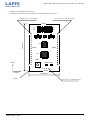
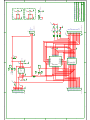
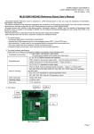
FEBL610Q111_RB-01 ML610Q111/ML610Q112 Reference Board User’s Manual Issue Date: Oct 22, 2013 ML610Q111/ML610Q112 Reference Board User’s Manual NOTES No copying or reproduction of this document, in part or in whole, is permitted without the consent of LAPIS Semiconductor Co., Ltd. The content specified herein is subject to change for improvement without notice. Examples of application circuits, circuit constants and any other information contained herein illustrate the standard usage and operations of the Products. The peripheral conditions must be taken into account when designing circuits for mass production. Great care was taken in ensuring the accuracy of the information specified in this document. However, should you incur any damage arising from any inaccuracy or misprint of such information, LAPIS Semiconductor shall bear no responsibility for such damage. The technical information specified herein is intended only to show the typical functions of and examples of application circuits for the Products. LAPIS Semiconductor does not grant you, explicitly or implicitly, any license to use or exercise intellectual property or other rights held by LAPIS Semiconductor and other parties. LAPIS Semiconductor shall bear no responsibility whatsoever for any dispute arising from the use of such technical information. The Products specified in this document are intended to be used with general-use electronic equipment or devices (such as audio visual equipment, office-automation equipment, communication devices, electronic appliances and amusement devices). The Products specified in this document are not designed to be radiation tolerant. While LAPIS Semiconductor always makes efforts to enhance the quality and reliability of its Products, a Product may fail or malfunction for a variety of reasons. Please be sure to implement in your equipment using the Products safety measures to guard against the possibility of physical injury, fire or any other damage caused in the event of the failure of any Product, such as derating, redundancy, fire control and fail-safe designs. LAPIS Semiconductor shall bear no responsibility whatsoever for your use of any Product outside of the prescribed scope or not in accordance with the instruction manual. The Products are not designed or manufactured to be used with any equipment, device or system which requires an extremely high level of reliability the failure or malfunction of which may result in a direct threat to human life or create a risk of human injury (such as a medical instrument, transportation equipment, aerospace machinery, nuclear-reactor controller, fuel-controller or other safety device). LAPIS Semiconductor shall bear no responsibility in any way for use of any of the Products for the above special purposes. If a Product is intended to be used for any such special purpose, please contact a ROHM sales representative before purchasing. If you intend to export or ship overseas any Product or technology specified herein that may be controlled under the Foreign Exchange and the Foreign Trade Law, you will be required to obtain a license or permit under the Law. Copyright 2013 LAPIS Semiconductor Co., Ltd. FEBL610Q111_RB-01 1 ML610Q111/ML610Q112 Reference Board User’s Manual Preface This document (user’s manual) describes the explanation of the ML610Q111/ML610Q112 reference board. ML610Q111 reference board is equipped with the 8-bit microcontroller ML610Q111. ML610Q112 reference board is equipped with the 8-bit microcontroller ML610Q112. The following manuals are also available in addition to this user’s manual. Read them as necessary ML610Q111/ML610Q112 User’s Manual - Description of the ML610Q111/ML610Q112 uEASE User’s Manual - Description of the on-chip debug tool uEASE. FEBL610Q111_RB-01 2 ML610Q111/ML610Q112 Reference Board User’s Manual ML610Q111/ML610Q112 Reference board is prepared by LAPIS SEMICONDUCTOR to have you study the operations of ML610Q111/ML610Q112. The board is only minimum necessary components are mounted on the board by LAPIS SEMICONDUCTOR for brief use of ML610Q111/ML610Q112. By using the board with "uEASE on-chip debug emulator" (hereinafter referred to "uEASE") and "free sample U8 Development Tools CD-ROM" which is bundled in the package of uEASE not only Software development/debugging but also writing Flash ROM in the devices are capable. This board also works in stand alone mode with external power suppy without uEASE. Before starting works with this board, read below carefully and understand notices. 1. The board features • Supports flash ROM programming (rewrite) and on-chip debugging (using RESET_N and TEST pins) • Selectable power supply (uEASE or peripheral) 2. The board hardware specifications Specific connection relationship of the mounted parts, please refer to the circuit diagram on page 7. Please refer to the reference schematics for detail on connections of each hardware parts. Embedded microcontroller ML610Q111 Reference Board U1: ML610Q111 ML610Q112 Reference Board U2: ML610Q112 J1: Jumper for RESET_N switch ( 3pin pin-header and short pin ) J2: Jumper for VDD switch ( 3pin pin-header and short pin ) CNU1-3: Connector for Peripheral (CNU1,2: 16pin, CNU3: 4pin) Embedded parts CNUE: Connector for on-chip debug emulator ( 14pin connector ) U3: Level shifter LED1-2: LED for display ( LED1: connect to PB7, LED2: connect to PC1) SW1: Tactile switch (connect to PA0) Operating voltage +3.3V to +5.5V Board size 35.56 x 58.42 mm *1 *2 *1: When you use PB7 and PC1, please cut the pattern between the pads of J5 and J6. *2: When you use PA0, please cut the pattern between the pads of J7. FEBL610Q111_RB-01 3 ML610Q111/ML610Q112 Reference Board User’s Manual 3. Reference board dimensions and layout The dimensions of this reference board and parts placement are shown below. 1pin (X, Y) = ( 2.54, 45.72 ) 1pin ( X, Y ) = ( 33.02, 45.72 ) CNuE 13 14 1 2 1 1 J1 U3 J2 58.42mm U1 CNU1 CNU2 U2 SW1 Y (mm) LED1 LED2 16 16 4 X (mm) Origen FEBL610Q111_RB-01 1 CNU3 35.56mm 1pin ( X, Y ) = ( 22.86, 2.54 ) 4 ML610Q111/ML610Q112 Reference Board User’s Manual 4. Notes on use (1) The information contained herein can change without notice owing to product and/or technical improvements. Before using the product, please make sure that the information being referred to is up-to-date. (2) Before using this board, read carefully and understand the contents of the ML610Q111/ML610Q112 user's manual and the uEASE user's manual. (3) The engineering sample of ML610Q111/ML610Q112 is mounted on the board. Therefore, please confirm the characteristic finally by using MP of ML610Q111/ML610Q112 and customer's mass production boards. (4) When you use uEASE, please set J1 jumper to the uE side. (5) When a power supply is given from the exterior, please be given by pin4 of CNU2 connector and set J2 jumper to the USR side. (6) When you set J2 jumper to the USR side and uEASE is connected, please turn ON the power supply of a board before starting uEASE. Moreover, please stop uEASE before turning off the power supply of a board. (7) When J2 jumper is set to the uE side, the power supply capacity of uEASE. is +3.3V/100mA. (8) This board has a conductivity pattern in the back, therefore it may short-circuits when it is used having put on the existing conductive component. FEBL610Q111_RB-01 5 A B C 1 1 2 3 4 5 6 7 8 9 10 11 12 13 14 15 16 A2-16PA-2.54DSA(71) PC0 RESET_N TEST PB0 PB1 PB2 PB3 PA2 TESTF PC3 PD0 PD1 NC4 PD2 PD3 PD4 GND CNU1 1 2 3 4 5 6 7 8 9 10 11 12 13 14 PSM-420336-07 VTref Vss Vpp Vss RESET_N Vss TEST Vss VDDL Vss N.C. Vss 3.3VOUT N.C. CNuE UEVDD R4 0 VPP GND C5 0.1U UEVDD UEVDD 2 GND 1 3 4 3 2 1 USRVDD 2 A1 OE VCCB B1 USR J2 USR J1 uE 2 TXS0102DCT A2 VCCA GND B2 U3 1 3 uE 5 6 7 8 2 1 2 3 4 5 6 7 8 1 2 3 4 5 6 7 8 9 10 TEST PD1 PB0 NC4 PB1 PB2 PB3 PA2 U2 RESET PWR UEVDD 10K GND R2 D 1 GND C6 0.1U J3 32 31 30 29 28 27 26 25 RESET_N PD0 PC0 PC4 PC5 PC1 PC6 PA0 TESTF PD2 PC3 PD3 PD4 PC2 PD5 PA1 ML610Q111 PC0 RESET_N TEST PB0 PB1 PB2 PB3 PA2 TESTF PC3 U1 PC1 PA0 PB7 VDD VSS PB6 PB5 PB4 PA1 PC2 9 10 11 12 13 14 15 16 J4 24 23 22 21 20 19 18 17 20 19 18 17 16 15 14 13 12 11 ML610Q112 PB7 PC7 VDD VSS NC20 PB6 PB5 PB4 VDD GND VDD GND VDD 3 3 GND VDD RESET_N TEST GND R3 R1 PC1 PA0 PB7 VDD VSS PB6 PB5 PB4 PA1 PC2 PC4 PC5 PC6 PC7 NC20 PD5 GND A2-16PA-2.54DSA(71) CNU2 SW1 1 3 2 4 SKHUALE010 LED2 SML-210DT LED1 SML-210DT A2-5PA-2.54DSA(71) 1 2 3 4 5 6 7 8 9 10 11 12 13 14 15 16 USRVDD J7 J6 J5 GND 1 2 3 4 CNU3 680 680 VDD C1 0.01U C2 0.01U TP1 LC-2-G(R) C8 4.7U C7 4.7U GND GND C4 0.1U C3 0.1U TP2 LC-2-G(G) GND VPP GND VPP SHEET DWG NO 6 4 of 6 QTS-11585 ML610Q111/Q112 3-21-2013_11:26 2.0 REV ML610Q111/Q112 REFERENCE BOARD APPLICATION TITLE LAPIS Semiconductor Co., Ltd. USRVDD USRVDD GND VDD Capacitor for U2 GND VDD Capacitor for U1 4 A B C D