1
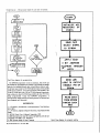
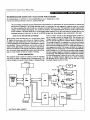
B. Electrochem 3(1) January-Februay 1987 pp 79-83
HICROPROCESSOR BASED LIFE CYCLE TESTER FOR BATTERIES
M PANDIAMMAL, K MUTHU, K R RAMAKRISHNAN and Y MAHADEVA IYER
Zentral Electrochemical Research Institute, Karaikudi-623 006
Life cycle testing of batteries requires sophisticated instrumentation for measurement of various parameters to evaluate the
performance of batteries in the chargeldischarge mode in a production line and logging the measured values for carrying
out data processing either with the help of a computer connected off line or on line. The parameters normally measured are
voltage, current (chargingldischarging). time, number of cycles etc. The measurements are carried out usually under constant
current condition. This paper deals with a microprocessor based charging unit for life cycle testing of storage cells and the
deve\oped software is fused with the help of the EPROM programmer whose design is also incorporated in this paper.
LIFE CYCLE TESTER FOR BATTERIES
r
ne present system described here is a microprocessor based
battery life cycle tester, with software for fixing the charge/
iischuge cycle and multiplexing of cells upto 256 nos. The unit
s easily expandable with proper addition of peripherals to evaluate
any paramettr. Software modification can be easily carried out
mlike in other rigid modules, to meet any specific testing demand.
Since the development of the storage cells being an ongoing proiect, the present system described here enables acquiring and logging of a large number of data for further processing.
SYSTEM DESCRIPTION
The proposed system consists of scanning a series of individual
:ells which are either in changing mode or discharge mode. The
:ells are charged with constant current chargers or charging through
-
I I
?-A&
-MULE
TIMER
62s
UP
0085
-
fi
KEYBOARD
Fig. 1: Battery tester schematic
&-
I I,
resistors or SCRs. The cells are also discharged under constant current or through a resistor or through SCRs. The individual cell
voltages scanned are logged in RAMS which are expanded upto
the level required using the bus expansion facility of SDK 85 kit.
The set high voltage (El) is compared every time during charging
and the cells are stopped for charging at a high level upto 3 volts
and reversed to discharging mode. Every charge and discharge cycle is logged and recorded. The timing is obtained for charge and
discharge cycle from an 8253 timer if constant time chargefischarge
mode is carried out, or if the limits are exceeded during charging,
the tima reading is logged for reaching the voltage limits of charge
and discharge. The independent timer thus enables more flexibility to the microprocessor to attend to service calls as well as sampling only. A detailed schematic diagram for a simple cell charge
and discharge cycle is given in Fig.1 and the flow chart of the
developed program is given in Fig.;.
Pandiarnrnal eta1 - Microprocessor based life cycle tester for batteries
the charging mode also, the charging is maintained at I amp.
through electronic resistor.
in hrs l sacond two b y i u arc in .riul
4-
YES
MVI, A
00
r
YES
G'
CYCLES
I
f
No
= MO OC
CYCLES .REQUIRED
Fig.2: Flow chart for constant time mode
FUNCTIONAL DESCRIPTION
When the instrument is switched on,it changes the mode of testing
to discharging mode. Then the discharge time and charge~imein
hours and minutes are fed into the microprocessor through
keyboard. Then the microprocessor will measure the cell voltage
for every I sec. through A/D convertor 8703 and compares the
lower limit of the cell voltage (E2) i.e., upto 1V. After discharge
time is over, it will switch over to charging mode. The'battery will
be changed to charging modc, even before discharge time is over
if the cell voltage comes below lower limit. In the charging mode
a d.c. power supply at 1 amp current rating is connected to charge
the battery (El), as long as the battery voltage is below the upper
limit (El) upto 3V. For one cycle, one discharge and one charge
operations are taken.
The battery will be switched over between discharge and charge
modes till it reaches no. of cycles (No) for which the battery is
to be put under testing. Once it reaches the required no. of cycles,
then the system will come to stop. In the discharging mode, the
discharge current is I amp. A D.C. resistor is used as load. 1n
80 B. Electrochem 3(1) Jan-Feb 1987
The system is built around SDK 85 with bus expansion for additional memory upto 8K bytes 11J]. A programmable timer 8253
is used in hardware interrupt mode. Most part of the
microprocessor time is used for cell voltage monitoring and comparing with set limits (El, E2, TI & T2). The counter 0 and counter
1 are used in mode 3 and counter 2 is used in mode 0. The bytes
stored in counters are in BCD form. The output of counter 0 is
clock input to counter 1 and output of counter 1 is clock input
to counter 2 and output of counter 2 is used for RST 7.5 interrupt. The clock output from microprocessor is given to counter
0 clock input. The charge/discharge time is fed into microprocessor
in BCD form. That time byte is converted into number i.e. minutes
(say 1 hour ten minutes = 70 minutes). This time in minutes in
BCD form is stored in counter 2 of 8253. The period of clock input to counter 2 is made equivalent to 1 minute, i.e. frequency
of the clock input to counter 2 is 1/60 Hz. So a pulse output will
appear at the putput pin of counter 2 Which will interrupt the
microprocessor at the end of TC (terminal count) of counter 2.
i.e. at the end of charge/discharge time. At location 20 CE a
microprocessor instruction is written to a subroutine program which
changes the mode of the battery. Multiplexer 16% A/D converter
8703 and sample/hold amplifier are used to select batteries and
to monitor the battery voltage. Port A of 8255 is used for outputting signals to electronic resistors. The 6 digit display available at
the kit will display the cell voltage in address field and display the
charge/discharge mode in the data field.
The test system described in this paper is capable of carrying
out life cycle testing of nickel-zinc cells to a minimum of one to
a maximum of 8 Nos. It could be expanded to 256. The instrument can also be easily expanded to record data such as
temperature, state of charge, capacitance, internal resistance etc.
for which work is being carried out in this lab.
The specifications are as follows for the testing system.
Mode: I . Constant time charging/discharging
2. Fixed number of cycles of charging/discharging
3. Endurance mode, voltage sensing mode and recording
maximum number of cycles
Charging cutoff voltage (El) : upto 3 volts
Discharging cutoff voltage (E2) : upto 1 volt
Charging/discharging current
: 500 mA to 10 A
for each cycle
Max. No. of cells to be
connected
: 8 (256)
Programme. listing can be supplied on request.
EPROM PROGRAMMER
In a computer or in a microprocessor based system memories are
required for storing informations like data, instructions etc. @,4].
ROM or EPROM is basically a non-volatile memory. This
means, even when the power to the memory is switched off, the
stored contents are retained. The contents. of ROM are either
~
L xuoa
Fg.3:Circuit diagram for EPROM programmer
blown by the manufaduras at the time of manufacturing or by 4. Load the informations (to be blown into 2716) in RAM location
starting from 8000
the user with the aidof specialp~ogrammasliketheoaepresented
here. To meet the changing req - ofthew.Erasabkand 5. Execute the program mess, Go. 2NM. EXE)
Reprogrammble R d Only Memories - EPROM chips are 6 . Xemove + 25V supply
+ 5 v supply
Now the information has been transferrd from RAM to
EPROM and stored.
7. Remove
avaihble.
The prol;.r;MM-d wnslsrs of 8255 PPI chip, the manory chip
to be programmed and a push butLon swaeh to wnmct a + 25V
READING THE INFORMATION FR6M EPROM
or + 5V supply to the program pin of 2716. It is shown in Fw.
3. The developed prunit bas a Euro edge wnnedor for After programmi'lg, it is necessary to verify the contents of
connectingtheunitwiththcSDK85micropocessorLitduring~ EPROM. For this the following stshould be followed in
~ramminsand program
sequma-
rq-
The flow chart of the monitor Wing to enable carrying out pr*
gramrning and readiog the EPROM is given in figs. 4 and 5
respectively.
For progmnming the fobwing steps are followed in sequence.
1. + 5V is applied to Pin No. 24 of 2716
2. + 25 V is applied to Pin No.21 of 2716
3. h a d theprogramin RAM(8155)fromstamngaddressaDOO
1. Apply
+ SV to Pin No.
+ 5V to Pin No.
24 of 2716
21 of 2716
3. Load the program in RAM from starting addrqss 2050
4. Exccrrte the program (Go, 2050. EXE)
5. Now the address will appear at the address field and the data
wiU appear at the data f ~ k of
l the display.
2. Apply
Thc software in the read mode provides facility to eiiher increment or damment the address by the use of separate incrementhg (Next) and decrementhg (EXE) keys, so as to enable forward
and backward search of the stored data in EPROM.
6. Ekvuchern 3(1), Jan-Feb 1987
81
Pandiammal eta1 -- Microprocessor based life cycle tester for batteries
REGISTER
PORlS
INITIALISE ACC
REGISTERS OF
PORTS
1 0 HlGH
LOGIC 10
OUTPUT ENABLE
P I N OF E P R O M
CIP 10
I
BE
I I B I T AOORESS
SELECT SIGNAL
TO EPROM
I
THROUGH
I
MOVE ME XI
8817 0 4 1 4 I0
BE PROGRAMMED
F R O M R A M TO
E P R O M THROUGH LATCH
I
u
APPLY NEXT
I1 BIT ADDRESS
APPLY LOW TO HlGH LOGIC
1 0 PROGRAMMING P I N OF
APPLY HlGH
TO LOW LffilC
TO PROGRAUMNG
C
I"
TO EPROM THROUGH
LATCH
I
SEND LOW
LOGIC TO OUTPUT
ENABLE PIN O F
EPROM
Fig.4 Flow diagram for programming
The EPROM programmer is easy to construct. The circuit can
be extended for programming of multiple 2716 EPROMs in parallel
and also for loading different data in the different chips as well.
In the latter case except for CE/PGM all like inputs of the parallel
2716s may be common. A TTL level program pulse applied to the
2716s CE/PGM input with VPP at 25V will program a particular
chip, while a low level CE/PGM input inhibits all other 2716 from
being programmed. Using this EPROM programmer, a
microprocessor based monitor and testing systems for batteries has
been designed and fabricated.
L
REFERENCES
1. A P Mathur, Introduction to microprocessors. Tata-McGraw
'
Mi11 (1985)
2. A.P. Malvino, Digital Computer electronics. Tata-McGraw Hill
(1 985)
3. MCS-85 (Intel) User's Manual, September 1978
4.8085 Microprocessor and the common peripheral LSIs that are
compatible with 8085. IISc, Bangalore
5. SDK System design kit user 'smonuol
#
READ DATA
FROM EPROM
THROUG DATA
BUS
I
-
82 0. Electrochem 3(11 Jan-Feb 1987
Fig.5: Flow diagram for program reading
Pandiammal eta1
-
Microprocessor based life cycle tester for batteries
EPROM PROGRAMMER
Wtware for r
Software
Locations OP
Code
Source 9utement
31 C2 20
Initialise stadspOinter
21 X2Xl Y2Yl Initialise H L register pair
X2 X I Low Address byte
Of
Y2 Y, High Address byte
RAM from where data is t o be
transferred to EPROM
1 1 A2 A l OBI Initialise DE register pair
A2Al Low Address byte
OBI High Address byte
1
)
EPROM t o where DATA is to be
transferred
B, is 0 t o 7
01 M I M2 ON2 Initialise BC register pair
M I M2 DATA IN HEX
ON2 DATA IN HEX X
No. of bytes to be transferred
N2 is 0 t o 7
MVI, A - 80 is the code number
for making port A, port B and port
C as output ports in zero mode
83 is the address of command
register of 8255
MOV A,D
AN1 to unmask page numbers
OR1 t o give High Logic to output
Enable pin of EPROM
STA, store this information at
RAM Location 20 A0 for later use
OUT 82
MOV A,E
OUT 81
MOV A,M - Move Data to be
programmed t o ACC
LDA, Retrieve the data stored at 20A0
OR1
OUT 82, Gives a HighIogic t o programming pin of EPROM
PUSH D
InitiaIise DE register pair with 00, 10
D = 10
E=00
Delay subroutine in SDK-85 monitor
POP D
LDA, Load ACC with rne contents
of 20A0
OUT 82, one data is now programmed at EPROM
INXH
INX D
DCX B
MOV A,B
ORA, C
JNZ, not a11 datas stored Jump t o 2010
RST 1 DISPLAY 8085 on the SDK
85 display t o indicate that programming is over.
e
~
~
~
m
n data
r e
d
Locations DP Code
Initialise stack pointer
Unrmsk RST 5.5
SIM
Make port A of 8255 as input port
and ports B & C as output ports
OUT 83
I N I T M U S E DE Register pair
XlX2 Low address
YlY2 High address
(page number)
where contents are to be read
MOV A,E
OUT 81
MOV A,D
ANI, TO unmask page number and
t o apply
Low logic t o output Enable pin of
EPROM
IN 80
PUSH D
CALL UFDDT
POPD
PUSH D
CALL UPDAD
EI
RDKBD
POPD
CPI (Next Button)
JNZ
INX D
CPI (EXEC Button)
JNZ
DCX D
B. Electrochem 3(1) Jan-Feb 1987
83