1
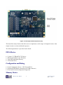
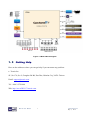
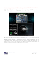
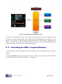
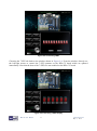
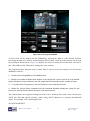
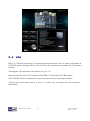
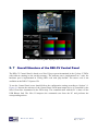
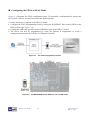
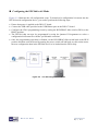
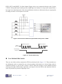
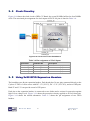
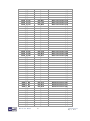
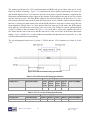
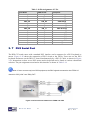
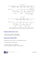
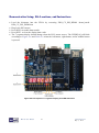
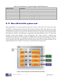
DE0-CV User Manual 1 www.terasic.com May 4, 2015 CONTENTS Chapter 1 Introduction ..................................................................................................... 3 1. 1 Package Contents ............................................................................................................................ 3 1. 2 DE0-CV System CD ....................................................................................................................... 4 1. 3 Layout and Components ................................................................................................................. 4 1. 4 Block Diagram of the Cyclone V Starter Board .............................................................................. 6 1. 5 Getting Help .................................................................................................................................... 7 Chapter 2 Control Panel ................................................................................................... 8 2. 1 Control Panel Setup......................................................................................................................... 8 2. 2 Controlling the LEDs, 7-segment Displays................................................................................... 10 2. 3 Switches and Push-buttons............................................................................................................ 12 2. 4 SDRAM Controller and Programmer ........................................................................................... 12 2. 5 SD Card ......................................................................................................................................... 14 2. 6 VGA .............................................................................................................................................. 15 2. 7 Overall Structure of the DE0-CV Control Panel ........................................................................... 16 Chapter 3 Using the Starter Kit ..................................................................................... 18 3. 1 Configuration of Cyclone V FPGA on DE0-CV ........................................................................... 18 3. 2 Using the LEDs and Switches ....................................................................................................... 21 3. 3 Using the 7-segment Displays ....................................................................................................... 25 3. 4 Clock Circuitry .............................................................................................................................. 27 3. 5 Using 2x20 GPIO Expansion Headers .......................................................................................... 27 3. 6 Using VGA.................................................................................................................................... 30 3. 7 PS/2 Serial Port ............................................................................................................................. 32 3. 8 Micro SD-Card Socket .................................................................................................................. 33 3. 9 Using SDRAM .............................................................................................................................. 34 Chapter 4 DE0-CV System Builder ............................................................................... 37 4. 1 Introduction ................................................................................................................................... 37 4. 2 General Design Flow..................................................................................................................... 37 4. 3 Using DE0-CV System Builder .................................................................................................... 38 DE0-CV User Manual 1 www.terasic.com May 4, 2015 Chapter 5 Examples of Advanced Demonstrations ................................................... 43 5. 1 DE0-CV Factory Configuration .................................................................................................... 43 5. 2 SDRAM Test in Nios II ................................................................................................................. 45 5. 3 SDRAM Test in Verilog ................................................................................................................ 48 5. 4 PS/2 Mouse Demonstration........................................................................................................... 49 5. 5 Micro SD Card file system read .................................................................................................... 53 5. 6 VGA Pattern .................................................................................................................................. 57 DE0-CV User Manual 2 www.terasic.com May 4, 2015 Chapter 1 Introduction The DE0-CV presents a robust hardware design platform built around the Altera Cyclone V FPGA, which is optimized for the lowest cost and power requirement for transceiver applications with industry-leading programmable logic for ultimate design flexibility. With Cyclone V FPGAs, you can get the power, cost, and performance levels you need for high-volume applications including protocol bridging, motor control drives and capture cards, and handheld devices. The DE0-CV development board includes hardware such as on-board USB Blaster, video capabilities and much more. By leveraging all of these capabilities, the DE0-CV is the perfect solution for showcasing, evaluating, and prototyping the true potential of the Altera Cyclone V FPGA. The DE0-CV contains all components needed to use the board in conjunction with a computer that runs the Microsoft Windows XP or later. 1. 1 Package Contents Figure 1-1 shows a photograph of the DE0-CV package. Figure 1-1 The DE0-CV package contents The DE0-CV package includes: The DE0-CV board 5V DC Power Supply Type A Male to Type B Male USB Cable DE0-CV User Manual 3 www.terasic.com May 4, 2015 1. 2 DE0-CV System CD The DE0-CV System CD contains the documentation and supporting materials, including the User Manual, Control Panel, System Builder, reference designs and device datasheets. User can download this System CD from the web (http://cd-de0-cv.terasic.com). 1. 3 Layout and Components This section presents the features and design characteristics of the board. A photograph of the board is shown in Figure 1-2 and Figure 1-3. It depicts the layout of the board and indicates the location of the connectors and key components. Figure 1-2 Development Board (top view) DE0-CV User Manual 4 www.terasic.com May 4, 2015 Figure 1-3 Development Board (bottom view) This board has many features that allow users to implement a wide range of designed circuits, from simple circuits to various multimedia projects. The following hardware is provided on the board: FPGA Device Cyclone V 5CEBA4F23C7N Device 49K Programmable Logic Elements 3080 Kbits embedded memory 4 Fractional PLLs Configuration and Debug Serial Configuration device – EPCS64 on FPGA On-Board USB Blaster (Normal type B USB connector) JTAG and AS mode configuration supported Memory Device DE0-CV User Manual 5 www.terasic.com May 4, 2015 64MB SDRAM, x16 bits data bus Communication PS/2 mouse/keyboard Connectors 2x20 GPIO Header D is p la y Uses a 4-bit resistor-network DAC With 15-pin high-density D-sub connector Micro SD Card Socket Provides SPI and 4-bit SD mode for Micro SD Card access Switches, Buttons and LEDs 10 LEDs 10 Slide Switches 4 Debounced Push Buttons 1 CPU reset Push Buttons Six 7-Segments Power 5V DC input 1. 4 Block Diagram of the Cyclone V Star ter Board Figure 1-4 gives the block diagram of the board. To provide maximum flexibility for the user, all connections are made through the Cyclone V FPGA device. Thus, the user can configure the FPGA to implement any system design. DE0-CV User Manual 6 www.terasic.com May 4, 2015 Figure 1-4 Board Block Diagram 1. 5 Getting Help Here are the addresses where you can get help if you encounter any problem: Terasic Inc. 9F., No.176, Sec.2, Gongdao 5th Rd, East Dist, Hsinchu City, 30070. Taiwan Email: [email protected] Tel.: +886-3-5750-880 Web: http://www.DE0-CV.terasic.com DE0-CV User Manual 7 www.terasic.com May 4, 2015 Chapter 2 Control Panel The DE0-CV board comes with a Control Panel program that allows users to access various components on the board from a host computer. The host computer communicates with the board through a USB connection. The program can be used to verify the functionality of components on the board or be used as a debug tool while developing any RTL code. This chapter first presents some basic functions of the Control Panel, then describes its structure in the block diagram form, and finally describes its capabilities. 2. 1 Control Panel Setup The Control Panel Software Utility is located in the directory “Tools/ControlPanel” in the DE0-CV System CD. It's free of installation, just copy the whole folder to your host computer and launch the control panel by executing the “DE0CV_ControlPanel.exe”. Specific control circuits should be downloaded to your FPGA board before the control panel can request it to perform required tasks. The program will call Quartus II tools to download the control circuit to the FPGA board through the USB-Blaster[USB-0] connection. To activate the Control Panel, perform the following steps: 1. Make sure Quartus II 14.0 or a later version is installed successfully on your PC. 2. Set the RUN/PROG switch to the RUN position. 3. Connect the USB cable provided to the USB Blaster port, connect the 5V power supply, and turn the power switch ON. 4. Start the executable DE0CV_ControlPanel.exe on the host computer. The Control Panel user interface shown in Figure 2-1 will appear. 5. The DE0CV_ControlPanel.sof bit stream is loaded automatically as soon as the DE0CV_ControlPanel.exe is launched. 6. In case of a disconnect, click on CONNECT where the .sof will be re-loaded onto the board. DE0-CV User Manual 8 www.terasic.com May 4, 2015 Please note that the Control Panel will occupy the USB port until you close that port; you cannot use Quartus II to download a configuration file into the FPGA until the USB port is closed. 7. The Control Panel is now ready to use; experience it by setting the ON/OFF status for some LEDs and observing the result on the DE0-CV board. Figure 2-1 The DE0-CV Control Panel The concept of the DE0-CV Control Panel is illustrated in Figure 2-2. The “Control Circuit” that performs the control functions is implemented in the FPGA board. It communicates with the Control Panel window, which is active on the host computer, via the USB Blaster link. The graphical interface is used to send commands to the control circuit. It handles all the requests and performs data transfers between the computer and the DE0-CV board. DE0-CV User Manual 9 www.terasic.com May 4, 2015 Figure 2-2 The DE0-CV Control Panel concept The DE0-CV Control Panel can be used to light up LEDs, change the values displayed on the 7-segment, monitor buttons/switches status, read/write the SDRAM Memory, output VGA color pattern to VGA monitor, read SD Card specification information. The feature of reading/writing a word or an entire file from/to the Memory allows the user to develop multimedia applications without worrying about how to build a Memory Programmer. 2. 2 Controlling the LEDs, 7-segment Displays A simple function of the Control Panel is to allow setting the values displayed on LEDs, 7-segment displays. Choosing the LED tab leads to the window in Figure 2-3. Here, you can directly turn the LEDs on or off individually or by clicking “Light All” or “Unlight All”. DE0-CV User Manual 10 www.terasic.com May 4, 2015 Figure 2-3 Controlling LEDs Choosing the 7-SEG tab leads to the window shown in Figure 2-4. From the window, directly use the left-right arrows to control the 7-SEG patterns on the DE0-CV board which are updated immediately. Note that the dots of the 7-SEGs are not enabled on the DE0-CV board. Figure 2-4 Controlling 7-SEG display DE0-CV User Manual 11 www.terasic.com May 4, 2015 The ability to set arbitrary values into simple display devices is not needed in typical design activities. However, it gives users a simple mechanism for verifying that these devices are functioning correctly in case a malfunction is suspected. Thus, it can be used for troubleshooting purposes. 2. 3 Switches and Push-buttons Choosing the Switches tab leads to the window in Figure 2-5. The function is designed to monitor the status of slide switches and push buttons in real time and show the status in a graphical user interface. It can be used to verify the functionality of the slide switches and push-buttons. Figure 2-5 Monitoring switches and buttons The ability to check the status of push-button and slide switch is not needed in typical design activities. However, it provides users a simple mechanism to verify if the buttons and switches are functioning correctly. Thus, it can be used for troubleshooting purposes. 2. 4 SDRAM Controller and Programmer The Control Panel can be used to write/read data to/from the SDRAM chips on the DE0-CV board. As shown below, we will describe how the SDRAM may be accessed; Click on the Memory tab and select “SDRAM” to reach the window in Figure 2-6. DE0-CV User Manual 12 www.terasic.com May 4, 2015 Figure 2-6 Accessing the SDRAM A 16-bit word can be written into the SDRAM by entering the address of the desired location, specifying the data to be written, and pressing the Write button. Contents of the location can be read by pressing the Read button. Figure 2-6 depicts the result of writing the hexadecimal value 06CA into offset address 200, followed by reading the same location. The Sequential Write function of the Control Panel is used to write the contents of a file into the SDRAM as follows: 1. Specify the starting address in the Address box. 2. Specify the number of bytes to be written in the Length box. If the entire file is to be loaded, then a checkmark may be placed in the File Length box instead of giving the number of bytes. 3. To initiate the writing process, click on the Write a File to Memory button. 4. When the Control Panel responds with the standard Windows dialog box asking for the source file, specify the desired file location in the usual manner. The Control Panel also supports loading files with a .hex extension. Files with a .hex extension are ASCII text files that specify memory values using ASCII characters to represent hexadecimal values. For example, a file containing the line 0123456789ABCDEF DE0-CV User Manual 13 www.terasic.com May 4, 2015 defines eight 8-bit values: 01, 23, 45, 67, 89, AB, CD, EF. These values will be loaded consecutively into the memory. The Sequential Read function is used to read the contents of the SDRAM and fill them into a file as follows: 1. Specify the starting address in the Address box. 2. Specify the number of bytes to be copied into the file in the Length box. If the entire contents of the SDRAM are to be copied (which involves all 64 Mbytes), then place a checkmark in the Entire Memory box. 3. Press Load Memory Content to a File button. 4. When the Control Panel responds with the standard Windows dialog box asking for the destination file, specify the desired file in the usual manner. 2. 5 SD Card The function is designed to read the identification and specification information of the SD Card. The 4-bit SD MODE is used to access the SD Card. This function can be used to verify the functionality of the SD Card Interface. Follow the steps below to perform the SD Card exercise: 1. Choosing the SD Card tab leads to the window in Figure 2-7. 2. Insert an SD Card to the DE0-CV board, and then press the Read button to read the SD Card. The SD Card‟s identification, specification, and file format information will be displayed in the control window. DE0-CV User Manual 14 www.terasic.com May 4, 2015 Figure 2-7 Reading the SD Card Identification and Specification 2. 6 VGA DE0-CV Control Panel provides VGA pattern function that allows users to output color pattern to LCD/CRT monitor using the DE0-CV board. Follow the steps below to generate the VGA pattern function: Choosing the VGA tab leads to the window in Figure 2-8. Plug a D-sub cable to the VGA connector of the DE0-CV board and LCD /CRT monitor. The LCD/CRT monitor will display the same color pattern on the control panel window. Click the drop down menu shown in Figure 2-8 where you can output the selected pattern individually. DE0-CV User Manual 15 www.terasic.com May 4, 2015 Figure 2-8 Controlling VGA display under Control Panel 2. 7 Overall Structure of the DE0-CV Control Panel The DE0-CV Control Panel is based on a Nios II Qsys system instantiated in the Cyclone V FPGA with software running on the on-chip memory. The software part is implemented in C code; the hardware part is implemented in Verilog HDL code with Qsys builder. The source code is not available on the DE0-CV System CD. To run the Control Panel, users should follow the configuration setting according to Section 3.1. Figure 2-9 depicts the structure of the Control Panel. Each input/output device is controlled by the Nios II Processor instantiated in the FPGA chip. The communication with the PC is done via the USB Blaster link. The Nios II interprets the commands sent from the PC and performs the corresponding actions. DE0-CV User Manual 16 www.terasic.com May 4, 2015 Figure 2-9 The block diagram of the DE0-CV control panel DE0-CV User Manual 17 www.terasic.com May 4, 2015 Chapter 3 Using the Starter Kit This chapter provides an instruction to use the board and describes the peripherals. 3. 1 Configuration of Cyclone V FPGA on DE0-CV The DE0-CV board contains a serial configuration device that stores configuration data for the Cyclone V FPGA. This configuration data is automatically loaded from the configuration device into the FPGA when powered on. Using the Quartus II software, it is possible to reconfigure the FPGA at any time, and it is also possible to change the non-volatile data that is stored in the serial configuration device. Both types of programming methods are described below. 1. JTAG programming: In this method of programming, named after the IEEE standards Joint Test Action Group, the configuration bit stream is downloaded directly into the Cyclone V FPGA. The FPGA will retain this configuration as long as power is applied to the board; the configuration information will be lost when the power is turned off. 2. AS programming: In this method, called Active Serial programming, the configuration bit stream is downloaded into the Altera EPCS64 serial configuration device. It provides non-volatile storage of the bit stream, so that the information is retained even when the power supply to the DE0-CV board is turned off. When the board‟s power is turned on, the configuration data in the EPCS64 device is automatically loaded into the Cyclone V FPGA. The sections below describe the steps to perform both JTAG and AS programming. For both methods the DE0-CV board is connected to a host computer via a USB cable. Using this connection, the board will be identified by the host computer as an Altera USB Blaster device. DE0-CV User Manual 18 www.terasic.com May 4, 2015 Configuring the FPGA in JTAG Mode Figure 3-1 illustrates the JTAG configuration setup. To download a configuration bit stream into the Cyclone V FPGA, you need to perform the following steps: Ensure that power is applied to the DE0-CV board Configure the JTAG programming circuit by setting the RUN/PROG slide switch (SW10) to the RUN position (See Figure 3-2) Connect the USB cable provided to the USB Blaster port on the DE0-CV board The FPGA can now be programmed by using the Quartus II Programmer to select a configuration bit stream file with the .sof filename extension Figure 3-1 Figure 3-2 The JTAG configuration scheme The RUN/PROG switch (SW10) is set in JTAG mode DE0-CV User Manual 19 www.terasic.com May 4, 2015 Configuring the EPCS64 in AS Mode Figure 3-3 illustrates the AS configuration setup. To download a configuration bit stream into the EPCS64 serial configuration device, you need to perform the following steps: Ensure that power is applied to the DE0-CV board. Connect the USB cable provided to the USB Blaster port on the DE0-CV board Configure the JTAG programming circuit by setting the RUN/PROG slide switch (SW10) to the PROG position. The EPCS64 chip can now be programmed by using the Quartus II Programmer to select a configuration bit stream file with the .pof filename extension. Once the programming operation is finished, set the RUN/PROG slide switch back to the RUN position and then reset the board by turning the power switch off and back on; this action causes the new configuration data in the EPCS64 device to be loaded into the FPGA chip. Figure 3-3 DE0-CV User Manual The AS configuration scheme 20 www.terasic.com May 4, 2015 Status LED The FPGA development board includes board-specific status LEDs to indicate board status. Please refer to Table 3-1 for the description of the LED indicator. Please refer to Figure 3-4 for detailed LED location. Table 3-1 Status LED Board Reference LED Name Description D15 3.3-V Power Illuminates when 3.3-V power is active. D16 ULED Illuminates when the on-board USB-Blaster is working Figure 3-4 Status LED position 3. 2 Using the LEDs and Switches User-Defined Push-buttons The board includes four user defined push-buttons and one FPGA reset button that allow users to interact with the Cyclone V device as shown in Figure 3-5. Each of these switches is debounced using a Schmitt Trigger circuit, as indicated in Figure 3-6. The five outputs called KEY0, KEY1, DE0-CV User Manual 21 www.terasic.com May 4, 2015 KEY2, KEY3 and RESET_N of the Schmitt Trigger devices are connected directly to the Cyclone V FPGA. Each push-button switch provides a high logic level when it is not pressed, and provides a low logic level when depressed. Since the push-button switches are debounced, they are appropriate for using as clocks or reset inputs in a circuit. Figure 3-5 Connections between the push-button and Cyclone V FPGA Pushbutton depressed Pushbutton released Before Debouncing Schmitt Trigger Debounced Figure 3-6 Switch debouncing User-Defined Slide Switch There are ten slide switches connected to FPGA on the board (See Figure 3-7). These switches are not debounced, and are assumed for use as level-sensitive data inputs to a circuit. Each switch is connected directly to a pin on the Cyclone V FPGA. When the switch is in the DOWN position (closest to the edge of the board), it provides a low logic level to the FPGA, and when the switch is in the UP position it provides a high logic level. DE0-CV User Manual 22 www.terasic.com May 4, 2015 Figure 3-7 Connections between the slide switches and Cyclone V FPGA User-Defined LEDs There are also ten user-controllable LEDs connected to FPGA on the board. Each LED is driven directly by a pin on the Cyclone V FPGA; driving its associated pin to a high logic level turns the LED on, and driving the pin low turns it off. Figure 3-8 shows the connections between LEDs and Cyclone V FPGA. Table 3-2, Table 3-3 and Table 3-4 list the pin assignment of user push-buttons, switches, and LEDs. DE0-CV User Manual 23 www.terasic.com May 4, 2015 Figure 3-8 Connections between the LEDs and Cyclone V FPGA Table 3-2 Pin Assignment of Push-buttons Signal Name KEY0 KEY1 KEY2 KEY3 RESET_N FPGA Pin No. PIN_U7 PIN_W9 PIN_M7 PIN_M6 PIN_P22 Description Push-button[0] Push-button[1] Push-button[2] Push-button[3] Push-button which connected to DEV_CLRN Pin of FPGA Table 3-3 Pin Assignment of Slide Switches Signal Name SW0 SW1 SW2 SW3 SW4 SW5 SW6 SW7 SW8 SW9 DE0-CV User Manual FPGA Pin No. PIN_U13 PIN_V13 PIN_T13 PIN_T12 PIN_AA15 PIN_AB15 PIN_AA14 PIN_AA13 PIN_AB13 PIN_AB12 24 Description Slide Switch[0] Slide Switch[1] Slide Switch[2] Slide Switch[3] Slide Switch[4] Slide Switch[5] Slide Switch[6] Slide Switch[7] Slide Switch[8] Slide Switch[9] www.terasic.com May 4, 2015 Table 3-4 Pin Assignment of LEDs Signal Name LEDR0 LEDR1 LEDR2 LEDR3 LEDR4 LEDR5 LEDR6 LEDR7 LEDR8 LEDR9 FPGA Pin No. PIN_AA2 PIN_AA1 PIN_W2 PIN_Y3 PIN_N2 PIN_N1 PIN_U2 PIN_U1 PIN_L2 PIN_L1 Description LED [0] LED [1] LED [2] LED [3] LED [4] LED [5] LED [6] LED [7] LED [8] LED [9] 3. 3 Using the 7-segment Displays The DE0-CV board has six 7-segment displays. These displays are paired to display numbers in various sizes. Figure 3-9 shows the connection of seven segments (common anode) to pins on Cyclone V FPGA. The segment can be turned on or off by applying a low logic level or high logic level from the FPGA, respectively. Each segment in a display is indexed from 0 to 6, with corresponding positions given in Figure 3-9. Table 3-5 shows the pin assignment of FPGA to the 7-segment displays. Figure 3-9 Connections between the 7-segment display HEX0 and the Cyclone V FPGA Table 3-5 Pin Assignment of 7-segment Displays Signal Name HEX00 HEX01 DE0-CV User Manual FPGA Pin No. PIN_U21 PIN_V21 25 Description Seven Segment Digit 0[0] Seven Segment Digit 0[1] www.terasic.com May 4, 2015 HEX02 HEX03 HEX04 HEX05 HEX06 HEX10 HEX11 HEX12 HEX13 HEX14 HEX15 HEX16 HEX20 HEX21 HEX22 HEX23 HEX24 HEX25 HEX26 HEX30 HEX31 HEX32 HEX33 HEX34 HEX35 HEX36 HEX40 HEX41 HEX42 HEX43 HEX44 HEX45 HEX46 HEX50 HEX51 HEX52 HEX53 HEX54 HEX55 HEX56 DE0-CV User Manual PIN_W22 PIN_W21 PIN_Y22 PIN_Y21 PIN_AA22 PIN_AA20 PIN_AB20 PIN_AA19 PIN_AA18 PIN_AB18 PIN_AA17 PIN_U22 PIN_Y19 PIN_AB17 PIN_AA10 PIN_Y14 PIN_V14 PIN_AB22 PIN_AB21 PIN_Y16 PIN_W16 PIN_Y17 PIN_V16 PIN_U17 PIN_V18 PIN_V19 PIN_U20 PIN_Y20 PIN_V20 PIN_U16 PIN_U15 PIN_Y15 PIN_P9 PIN_N9 PIN_M8 PIN_T14 PIN_P14 PIN_C1 PIN_C2 PIN_W19 26 Seven Segment Digit 0[2] Seven Segment Digit 0[3] Seven Segment Digit 0[4] Seven Segment Digit 0[5] Seven Segment Digit 0[6] Seven Segment Digit 1[0] Seven Segment Digit 1[1] Seven Segment Digit 1[2] Seven Segment Digit 1[3] Seven Segment Digit 1[4] Seven Segment Digit 1[5] Seven Segment Digit 1[6] Seven Segment Digit 2[0] Seven Segment Digit 2[1] Seven Segment Digit 2[2] Seven Segment Digit 2[3] Seven Segment Digit 2[4] Seven Segment Digit 2[5] Seven Segment Digit 2[6] Seven Segment Digit 3[0] Seven Segment Digit 3[1] Seven Segment Digit 3[2] Seven Segment Digit 3[3] Seven Segment Digit 3[4] Seven Segment Digit 3[5] Seven Segment Digit 3[6] Seven Segment Digit 4[0] Seven Segment Digit 4[1] Seven Segment Digit 4[2] Seven Segment Digit 4[3] Seven Segment Digit 4[4] Seven Segment Digit 4[5] Seven Segment Digit 4[6] Seven Segment Digit 5[0] Seven Segment Digit 5[1] Seven Segment Digit 5[2] Seven Segment Digit 5[3] Seven Segment Digit 5[4] Seven Segment Digit 5[5] Seven Segment Digit 5[6] www.terasic.com May 4, 2015 3. 4 Clock Circuitr y Figure 3-10 shows the clock circuit of DE0-CV Board, the crystal 50 MHz buffered to four 50MHz clock. The associated pin assignment for clock inputs to FPGA I/O pins is listed in Table 3-6. Figure 3-10 Clock circuit of the FPGA Board Table 3-6 Pin Assignment of Clock Inputs Signal Name CLOCK_50 CLOCK2_50 CLOCK3_50 CLOCK4_50 FPGA Pin No. PIN_M9 PIN_H13 PIN_E10 PIN_V15 Description 50 MHz clock input(Bank 3B) 50 MHz clock input(Bank 7A) 50 MHz clock input(Bank 8A) 50 MHz clock input(Bank 4A) 3. 5 Using 2x20 GPIO Expansion Headers The board has two 40-pin expansion headers. Each header has 36 user pins connected directly to the Cyclone V FPGA. It also comes with DC +5V (VCC5), DC +3.3V (VCC3P3), and two GND pins. Both 5V and 3.3V can provide a total of 5W power. Each pin on the expansion headers is connected to two diodes and a resistor for protection against high or low voltage level. Figure 3-11 shows the protection circuitry applied to all 2x36 data pins. Figure 3-11 shows the related schematics. Table 3-7 shows the pin assignment of two GPIO headers. DE0-CV User Manual 27 www.terasic.com May 4, 2015 Figure 3-11 Connections between the GPIO header and Cyclone V FPGA Figure 3-12 I/O distribution of the expansion headers Table 3-7 Pin Assignment of Expansion Headers Signal Name GPIO_0_D0 GPIO_0_D1 GPIO_0_D2 GPIO_0_D3 GPIO_0_D4 GPIO_0_D5 GPIO_0_D6 DE0-CV User Manual FPGA Pin No. PIN_N16 PIN_B16 PIN_M16 PIN_C16 PIN_D17 PIN_K20 PIN_K21 28 Description GPIO Connection 0[0] GPIO Connection 0[1] GPIO Connection 0[2] GPIO Connection 0[3] GPIO Connection 0[4] GPIO Connection 0[5] GPIO Connection 0[6] www.terasic.com May 4, 2015 GPIO_0_D7 GPIO_0_D8 GPIO_0_D9 GPIO_0_D10 GPIO_0_D11 GPIO_0_D12 GPIO_0_D13 GPIO_0_D14 GPIO_0_D15 GPIO_0_D16 GPIO_0_D17 GPIO_0_D18 GPIO_0_D19 GPIO_0_D20 GPIO_0_D21 GPIO_0_D22 GPIO_0_D23 GPIO_0_D24 GPIO_0_D25 GPIO_0_D26 GPIO_0_D27 GPIO_0_D28 GPIO_0_D29 GPIO_0_D30 GPIO_0_D31 GPIO_0_D32 GPIO_0_D33 GPIO_0_D34 GPIO_0_D35 GPIO_1_D0 GPIO_1_D1 GPIO_1_D2 GPIO_1_D3 GPIO_1_D4 GPIO_1_D5 GPIO_1_D6 GPIO_1_D7 GPIO_1_D8 GPIO_1_D9 GPIO_1_D10 GPIO_1_D11 GPIO_1_D12 GPIO_1_D13 GPIO_1_D14 GPIO_1_D15 GPIO_1_D16 GPIO_1_D17 DE0-CV User Manual PIN_K22 PIN_M20 PIN_M21 PIN_N21 PIN_R22 PIN_R21 PIN_T22 PIN_N20 PIN_N19 PIN_M22 PIN_P19 PIN_L22 PIN_P17 PIN_P16 PIN_M18 PIN_L18 PIN_L17 PIN_L19 PIN_K17 PIN_K19 PIN_P18 PIN_R15 PIN_R17 PIN_R16 PIN_T20 PIN_T19 PIN_T18 PIN_T17 PIN_T15 PIN_H16 PIN_A12 PIN_H15 PIN_B12 PIN_A13 PIN_B13 PIN_C13 PIN_D13 PIN_G18 PIN_G17 PIN_H18 PIN_J18 PIN_J19 PIN_G11 PIN_H10 PIN_J11 PIN_H14 PIN_A15 29 GPIO Connection 0[7] GPIO Connection 0[8] GPIO Connection 0[9] GPIO Connection 0[10] GPIO Connection 0[11] GPIO Connection 0[12] GPIO Connection 0[13] GPIO Connection 0[14] GPIO Connection 0[15] GPIO Connection 0[16] GPIO Connection 0[17] GPIO Connection 0[18] GPIO Connection 0[19] GPIO Connection 0[20] GPIO Connection 0[21] GPIO Connection 0[22] GPIO Connection 0[23] GPIO Connection 0[24] GPIO Connection 0[25] GPIO Connection 0[26] GPIO Connection 0[27] GPIO Connection 0[28] GPIO Connection 0[29] GPIO Connection 0[30] GPIO Connection 0[31] GPIO Connection 0[32] GPIO Connection 0[33] GPIO Connection 0[34] GPIO Connection 0[35] GPIO Connection 1[0] GPIO Connection 1[1] GPIO Connection 1[2] GPIO Connection 1[3] GPIO Connection 1[4] GPIO Connection 1[5] GPIO Connection 1[6] GPIO Connection 1[7] GPIO Connection 1[8] GPIO Connection 1[9] GPIO Connection 1[10] GPIO Connection 1[11] GPIO Connection 1[12] GPIO Connection 1[13] GPIO Connection 1[14] GPIO Connection 1[15] GPIO Connection 1[16] GPIO Connection 1[17] www.terasic.com May 4, 2015 GPIO_1_D18 GPIO_1_D19 GPIO_1_D20 GPIO_1_D21 GPIO_1_D22 GPIO_1_D23 GPIO_1_D24 GPIO_1_D25 GPIO_1_D26 GPIO_1_D27 GPIO_1_D28 GPIO_1_D29 GPIO_1_D30 GPIO_1_D31 GPIO_1_D32 GPIO_1_D33 GPIO_1_D34 GPIO_1_D35 PIN_J13 PIN_L8 PIN_A14 PIN_B15 PIN_C15 PIN_E14 PIN_E15 PIN_E16 PIN_F14 PIN_F15 PIN_F13 PIN_F12 PIN_G16 PIN_G15 PIN_G13 PIN_G12 PIN_J17 PIN_K16 GPIO Connection 1[18] GPIO Connection 1[19] GPIO Connection 1[20] GPIO Connection 1[21] GPIO Connection 1[22] GPIO Connection 1[23] GPIO Connection 1[24] GPIO Connection 1[25] GPIO Connection 1[26] GPIO Connection 1[27] GPIO Connection 1[28] GPIO Connection 1[29] GPIO Connection 1[30] GPIO Connection 1[31] GPIO Connection 1[32] GPIO Connection 1[33] GPIO Connection 1[34] GPIO Connection 1[35] 3. 6 Using VGA The DE0-CV board includes a 16-pin D-SUB connector for VGA output. The VGA synchronization signals are provided directly from the Cyclone V FPGA, and a 4-bit DAC using resistor network is used to produce the analog data signals (red, green, and blue). The associated schematic is given in Figure 3-13 and can support standard VGA resolution (640x480 pixels, at 25 MHz). Figure 3-13 Connections between the FPGA and VGA DE0-CV User Manual 30 www.terasic.com May 4, 2015 The timing specification for VGA synchronization and RGB (red, green, blue) data can be easily found on website nowadays. Figure 3-13 illustrates the basic timing requirements for each row (horizontal) displayed on a VGA monitor. An active-low pulse of specific duration is applied to the horizontal synchronization (hsync) input of the monitor, which signifies the end of one row of data and the start of the next. The data (RGB) output to the monitor must be off (driven to 0 V) for a time period called the back porch (b) after the hsync pulse occurs, which is followed by the display interval (c). During the data display interval the RGB data drives each pixel in turn across the row being displayed. Finally, there is a time period called the front porch (d) where the RGB signals must again be off before the next hsync pulse can occur. The timing of vertical synchronization (vsync) is similar to the one shown in Figure 3-14, except that a vsync pulse signifies the end of one frame and the start of the next, and the data refers to the set of rows in the frame (horizontal timing). Table 3-8 and Table 3-9 show different resolutions and durations of time period a, b, c, and d for both horizontal and vertical timing. The pin assignments between the Cyclone V FPGA and the VGA connector are listed in Table 3-10. Figure 3-14 VGA horizontal timing specification Table 3-8 VGA Horizontal Timing Specification VGA mode Horizontal Timing Spec Configuration Resolution(HxV) VGA(60Hz) 640x480 a(pixel b(pixel c(pixel d(pixel clock clock clock clock cycle) 96 cycle) 48 cycle) 640 cycle) 16 Pixel clock(MHz) 25 Table 3-9 VGA Vertical Timing Specification VGA mode Vertical Timing Spec Configuration VGA(60Hz) Resolution(HxV) 640x480 DE0-CV User Manual a(lines) 2 31 b(lines) 33 c(lines) 480 d(lines) 10 Pixel clock(MHz) 25 www.terasic.com May 4, 2015 Table 3-10 Pin Assignment of VGA Signal Name FPGA Pin No. Description VGA_R0 PIN_A9 VGA Red[0] VGA_R1 PIN_B10 VGA Red[1] VGA_R2 PIN_C9 VGA Red[2] VGA_R3 PIN_A5 VGA Red[3] VGA_G0 PIN_L7 VGA Green[0] VGA_G1 PIN_K7 VGA Green[1] VGA_G2 PIN_J7 VGA Green[2] VGA_G3 PIN_J8 VGA Green[3] VGA_B0 VGA_B1 VGA_B2 VGA_B3 VGA_HS VGA_VS PIN_B6 PIN_B7 PIN_A8 PIN_A7 PIN_H8 PIN_G8 VGA Blue[0] VGA Blue[1] VGA Blue[2] VGA Blue[3] VGA H_SYNC VGA V_SYNC 3. 7 PS/2 Serial Por t The DE0-CV board comes with a standard PS/2 interface and a connector for a PS/2 keyboard or mouse. Figure 3-15 shows the connection of PS/2 circuit to the FPGA. Users can use the PS/2 keyboard and mouse on the DE0-CV board simultaneously by a PS/2 Y-Cable, as shown in Figure 3-16. Instructions on how to use PS/2 mouse and/or keyboard can be found on various educational websites. The pin assignment associated to this interface is shown in Table 3-11. Note: If users connect only one PS/2 equipment, the PS/2 signals connected to the FPGA I/O should be “PS2_CLK” and “PS2_DAT”. Figure 3-15 Connections between the FPGA and PS/2 DE0-CV User Manual 32 www.terasic.com May 4, 2015 Figure 3-16 Y-Cable for using keyboard and mouse simultaneously Table 3-11 Pin Assignment of PS/2 Signal Name PS2_CLK PS2_DAT PS2_CLK2 PS2_DAT2 FPGA Pin No. PIN_D3 PIN_G2 PIN_E2 PIN_G1 Description PS/2 Clock PS/2 Data PS/2 Clock (reserved for second PS/2 device) PS/2 Data (reserved for second PS/2 device) 3. 8 Micro SD-Card Socket The development board supports Micro SD card interface using x4 data lines. Figure 3-17 shows the related signals connections between the SD Card and Cyclone V FPGA and Figure 3-18 shows micro SD card plug-in position. Finally, Table 3-12 lists all the associated pins. Figure 3-17 Connection between the SD Card Socket and Cyclone V FPGA DE0-CV User Manual 33 www.terasic.com May 4, 2015 Figure 3-18 Micro SD Card Table 3-12 Pin Assignment of Micro SD Card Socket Signal Name SD_CLK SD_CMD SD_DATA0 SD_DATA1 SD_DATA2 SD_DATA3 FPGA Pin No. PIN_H11 PIN_B11 PIN_K9 PIN_D12 PIN_E12 PIN_C11 Description Serial Clock Command, Response Serial Data 0 Serial Data 1 Serial Data 2 Serial Data 3 3. 9 Using SDRAM The board features 64MB of SDRAM with a single 64MB (32Mx16) SDRAM chip. The chip consists of 16-bit data line, control line, and address line connected to the FPGA. This chip uses the 3.3V LVCMOS signaling standard. Connections between the FPGA and SDRAM are shown in Figure 3-19, and the pin assignment is listed in Table 3-13. DE0-CV User Manual 34 www.terasic.com May 4, 2015 Figure 3-19 Connections between the FPGA and SDRAM Table 3-13 Pin Assignment of SDRAM Signal Name DRAM_ADDR0 FPGA Pin No. Description PIN_W8 SDRAM Address[0] DRAM_ADDR1 PIN_T8 SDRAM Address[1] DRAM_ADDR2 PIN_U11 SDRAM Address[2] DRAM_ADDR3 PIN_Y10 SDRAM Address[3] DRAM_ADDR4 PIN_N6 SDRAM Address[4] DRAM_ADDR5 PIN_AB10 SDRAM Address[5] DRAM_ADDR6 PIN_P12 SDRAM Address[6] DRAM_ADDR7 PIN_P7 SDRAM Address[7] DRAM_ADDR8 PIN_P8 SDRAM Address[8] DRAM_ADDR9 PIN_R5 SDRAM Address[9] DRAM_ADDR10 PIN_U8 SDRAM Address[10] DRAM_ADDR11 PIN_P6 SDRAM Address[11] DRAM_ADDR12 PIN_R7 SDRAM Address[12] DRAM_DQ0 PIN_Y9 SDRAM Data[0] DRAM_DQ1 PIN_T10 SDRAM Data[1] DRAM_DQ2 PIN_R9 SDRAM Data[2] DRAM_DQ3 PIN_Y11 SDRAM Data[3] DRAM_DQ4 PIN_R10 SDRAM Data[4] DRAM_DQ5 PIN_R11 SDRAM Data[5] DRAM_DQ6 PIN_R12 SDRAM Data[6] DRAM_DQ7 PIN_AA12 SDRAM Data[7] DRAM_DQ8 PIN_AA9 SDRAM Data[8] DRAM_DQ9 PIN_AB8 SDRAM Data[9] DE0-CV User Manual 35 www.terasic.com May 4, 2015 DRAM_DQ10 PIN_AA8 SDRAM Data[10] DRAM_DQ11 PIN_AA7 SDRAM Data[11] DRAM_DQ12 PIN_V10 SDRAM Data[12] DRAM_DQ13 PIN_V9 SDRAM Data[13] DRAM_DQ14 PIN_U10 SDRAM Data[14] DRAM_DQ15 PIN_T9 SDRAM Data[15] DRAM_BA0 PIN_T7 SDRAM Bank Address[0] DRAM_BA1 PIN_AB7 SDRAM Bank Address[1] DRAM_LDQM PIN_U12 SDRAM byte Data Mask[0] DRAM_UDQM PIN_N8 SDRAM byte Data Mask[1] DRAM_RAS_N PIN_AB6 DRAM_CAS_N PIN_V6 SDRAM Column Address Strobe DRAM_CKE PIN_R6 SDRAM Clock Enable DRAM_CLK PIN_AB11 SDRAM Clock DRAM_WE_N PIN_AB5 SDRAM Write Enable DRAM_CS_N PIN_U6 SDRAM Chip Select DE0-CV User Manual SDRAM Row Address Strobe 36 www.terasic.com May 4, 2015 Chapter 4 DE0-CV System Builder This chapter describes how users can create a custom design project with the tool named DE0-CV System Builder. 4. 1 Introduction The DE0-CV System Builder is a Windows-based utility. It is designed to help users create a Quartus II project for DE0-CV within minutes. The generated Quartus II project files include: Quartus II project file (.qpf) Quartus II setting file (.qsf) Top-level design file (.v) Synopsis design constraints file (.sdc) Pin assignment document (.htm) The above files generated by the DE0-CV System Builder can also prevent occurrence of situations that are prone to compilation error when users manually edit the top-level design file or place pin assignment. The common mistakes that users encounter are: Board is damaged due to incorrect bank voltage setting or pin assignment. Board is malfunctioned because of wrong device chosen, declaration of pin location or direction is incorrect or forgotten. Performance degradation due to improper pin assignment. 4. 2 General Design Flow This section provides an introduction to the design flow of building a Quartus II project for DE0-CV under the DE0-CV System Builder. The design flow is illustrated in Figure 4-1. The DE0-CV System Builder will generate two major files, a top-level design file (.v) and a Quartus II setting file (.qsf) after users launch the DE0-CV System Builder and create a new project according to their design requirements DE0-CV User Manual 37 www.terasic.com May 4, 2015 The top-level design file contains a top-level Verilog HDL wrapper for users to add their own design/logic. The Quartus II setting file contains information such as FPGA device type, top-level pin assignment, and the I/O standard for each user-defined I/O pin. Finally, the Quartus II programmer is used to download .sof file to the development board via JTAG interface. Figure 4-1 Design flow of building a project from the beginning to the end 4. 3 Using DE0-CV System Builder This section provides the procedures in details on how to use the DE0-CV System Builder. Install and Launch the DE0-CV System Builder The DE0-CV System Builder is located in the directory: “Tools\SystemBuilder” of the DE0-CV System CD. Users can copy the entire folder to a host computer without installing the utility. A window will pop up, as shown in Figure 4-2, after executing the DE0-CV SystemBuilder.exe on the host computer. DE0-CV User Manual 38 www.terasic.com May 4, 2015 Figure 4-2 The GUI of DE0-CV System Builder Enter Project Name Enter the project name in the circled area, as shown in Figure 4-3. The project name typed in will be assigned automatically as the name of your top-level design entity. Figure 4-3 Enter the project name DE0-CV User Manual 39 www.terasic.com May 4, 2015 System Configuration Users are given the flexibility in the System Configuration to include their choice of components in the project, as shown in Figure 4-4. Each component onboard is listed and users can enable or disable one or more components at will. If a component is enabled, the DE0-CV System Builder will automatically generate its associated pin assignment, including the pin name, pin location, pin direction, and I/O standard. Figure 4-4 System configuration group GPIO Expansion If users connect any Terasic GPIO-based daughter card to the GPIO connector(s) on DE0-CV, the DE0-CV System Builder can generate a project that include the corresponding module, as shown in Figure 4-5. It will also generate the associated pin assignment automatically, including pin name, pin location, pin direction, and I/O standard. DE0-CV User Manual 40 www.terasic.com May 4, 2015 Figure 4-5 GPIO expansion group The “Prefix Name” is an optional feature that denote the pin name of the daughter card assigned in your design. Users may leave this field blank. Project Setting Management The DE0-CV System Builder also provides the option to load a setting or save users‟ current board configuration in .cfg file, as shown in Figure 4-6. Figure 4-6 Project Settings DE0-CV User Manual 41 www.terasic.com May 4, 2015 Project Generation When users press the Generate button as shown in Figure 4-7, the DE0-CV System Builder will generate the corresponding Quartus II files and documents, as listed in Table 4-1: Figure 4-7 Generate Quartus Project Table 4-1 Files generated by the DE0-CV System Builder No. 1 Filename Description Top level Verilog HDL file for Quartus II <Project name>.v 2 <Project name>.qpf Quartus II Project File 3 <Project name>.qsf Quartus II Setting File 4 <Project name>.sdc Synopsis Design Constraints file for Quartus II 5 <Project name>.htm Pin Assignment Document Users can add custom logic into the project in Quartus II and compile the project to generate the SRAM Object File (.sof). DE0-CV User Manual 42 www.terasic.com May 4, 2015 Chapter 5 Examples of Advanced Demonstrations This chapter provides examples of advanced designs implemented by RTL or Qsys on the DE0-CV board. These reference designs cover the features of peripherals connected to the FPGA, such as PS/2, SDRAM, and SD card. All the associated files can be found in the directory \Demonstrations of DE0-CV System CD. Installation of Demonstrations To install the demonstrations on your computer: Copy the folder Demonstrations to a local directory of your choice. It is important to make sure the path to your local directory contains NO space. Otherwise it will lead to error in Nios II. Note : Quartus II v14.0 or later is required for all DE0-CV demonstrations to support Cyclone V FPGA device. 5. 1 DE0-CV Factor y Configuration The DE0-CV board has a default configuration bit-stream pre-programmed, which demonstrates some of the basic features onboard. The setup required for this demonstration and the location of its files are shown below. Demonstration File Locations Project directory: DE0_CV_Default Bitstream used: DE0_CV_Default.sof ,DE0_CV_Default.pof or DE0_CV_Default.jic Demonstration Setup and Instructions DE0-CV User Manual 43 www.terasic.com May 4, 2015 Power on the DE0-CV board with the USB cable connected to the USB-Blaster port. If necessary (that is, if the default factory configuration is not currently stored in the EPCS device), download the bit stream to the board via JTAG interface. You should now be able to observe the 7-segment displays are showing a sequence of characters, and the red LEDs are blinking. Press FPGA_RESET to make LEDs and 7 SEGs all light on. If the VGA D-SUB connector is connected to a VGA display, it would show a color picture. Restore Factory Configuration Configuring the EPCS64 in AS Mode 1. Ensure that power is applied to the DE0_CV board. 2. Connect the supplied USB cable to the USB Blaster port on the DE0-CV board 3. Configure the JTAG programming circuit by setting the RUN/PROG slide switch (SW10) to the PROG position. 4. Execute the demo batch file “pof_DE0_CV_Default.bat” for USB-Blaster under the batch file folder, DE0_CV_Default /demo_batch. 5. Once the programming operation is finished, set the RUN/PROG slide switch back to the RUN position and then reset the board by turning the power switch off and back on; this action causes the new configuration data in the EPCS64 device to be loaded into the FPGA chip. Configuring the EPCS64 with .JIC File 1. Ensure that power is applied to the DE0_CV board. 2. Connect the supplied USB cable to the USB Blaster port on the DE0-CV board. 3. Execute the demo batch file “ DE0_CV_Default.bat” for USB-Blaster under the batch file folder, DE0_CV_Default /demo_batch. 4. As shown in Figure 5-1, It is able to not only load the bit stream into the FPGA in command line, but also program or erase .jic file to the EPCS by executing the batch file. 5. If users want to program a new design into the EPCS device, an easy method is to copy the new .sof file (file name must be DE0_CV_Default.sof) into the demo_batch folder and execute the DE0_CV_Default.bat. Option “2” will convert the .sof to .jic and option”3” will program .jic file into the EPCS device. DE0-CV User Manual 44 www.terasic.com May 4, 2015 Figure 5-1 Command line of the batch file to program the FPGA and EPCS device 5. 2 SDRAM Test in Nios II There are many applications using SDRAM as a temporary storage. Both hardware and software designs are provided to illustrate how to perform memory access in Qsys in this demonstration. It also shows how Altera‟s SDRAM controller IP accesses SDRAM and how the Nios II processor reads and writes the SDRAM for hardware verification. The SDRAM controller handles complex aspects of accessing SDRAM such as initializing the memory device, managing SDRAM banks, and keeping the devices refreshed at certain interval. System Block Diagram Figure 5-2 shows the system block diagram of this demonstration. The system requires a 50 MHz clock input from the board. The SDRAM controller is configured as a 64MB controller. The working frequency of the SDRAM controller is 143 MHz, and the Nios II program is running on the on-chip memory. DE0-CV User Manual 45 www.terasic.com May 4, 2015 Figure 5-2 Block diagram of the SDRAM test in Nios II The system flow is controlled by a program running in Nios II. The Nios II program writes test patterns into the entire 64MB of SDRAM first before calling the Nios II system function, alt_dcache_flush_all, to make sure all the data are written to the SDRAM. It then reads data from the SDRAM for data verification. The program will show the progress in nios-terminal when writing/reading data to/from the SDRAM. When the verification process reaches 100%, the result will be displayed in nios-terminal. Design Tools Quartus II v14.0 Nios II Eclipse v14.0 Demonstration Source Code Quartus project directory: DE0_CV_SDRAM_Nios_Test Nios II Eclipse directory: DE0_CV_SDRAM_Nios_Test \Software Nios II Project Compilation Click “Clean” from the “Project” menu of Nios II Eclipse before compiling the reference design in Nios II Eclipse. DE0-CV User Manual 46 www.terasic.com May 4, 2015 Demonstration Batch File The files are located in the director: \DE0_CV_SDRAM_Nios_Test \demo_batch. The folder includes the following files: Batch file for USB-Blaster II : DE0_CV_SDRAM_Nios_Test.bat and DE0_CV_SDRAM_Nios_Test.sh FPGA configuration file : DE0_CV_SDRAM_Nios_Test.sof Nios II program: DE0_CV_SDRAM_Nios_Test.elf Demonstration Setup Quartus II v14.0 and Nios II v14.0 must be pre-installed on the host PC. Power on the DE0_CV board. Connect the DE0_CV board (J13) to the host PC with a USB cable and install the USB-Blaster driver if necessary. Execute the demo batch file “DE0_CV_SDRAM_Nios_Test.bat” from the directory DE0_CV_SDRAM_Nios_Test\demo_batch After the program is downloaded and executed successfully, a prompt message will be displayed in nios2-terminal. Press any button (KEY3~KEY0) to start the SDRAM verification process. Press KEY0 to run the test continuously. The program will display the test progress and result, as shown in Figure 5-3. Figure 5-3 Display of progress and result for the SDRAM test in Nios II DE0-CV User Manual 47 www.terasic.com May 4, 2015 5. 3 SDRAM Test in Verilog DE0_CV system CD offers another SDRAM test with its test code written in Verilog HDL. The memory size of the SDRAM bank tested is still 64MB. Function Block Diagram Figure 5-4 shows the function block diagram of this demonstration. The SDRAM controller uses 50 MHz as a reference clock and generates 100 MHz as the memory clock. Figure 5-4 Block diagram of the SDRAM test in Verilog RW_Test module writes the entire memory with a test sequence first before comparing the data read back with the regenerated test sequence, which is same as the data written to the memory. KEY0 triggers test control signals for the SDRAM, and the LEDs will indicate the test result according to Table 5-1. Design Tools Quartus II v14.0 Demonstration Source Code Project directory: DE0_CV_SDRAM_RTL_Test Bitstream used: DE0_CV_SDRAM_RTL_Test.sof DE0-CV User Manual 48 www.terasic.com May 4, 2015 Demonstration Batch File Demo batch file folder: \DE0_CV_SDRAM_RTL_Test\demo_batch The directory includes the following files: Batch file: DE0_CV_SDRAM_RTL_Test.bat FPGA configuration file: DE0_CV_SDRAM_RTL_Test.sof Demonstration Setup Quartus II v14.0 must be pre-installed to the host PC. Connect the DE0_CV board (J13) to the host PC with a USB cable and install the USB-Blaster II driver if necessary Power on the DE0_CV board. Execute the demo batch file “ DE0_CV_SDRAM_RTL_Test.bat” from the directoy \DE0_CV_SDRAM_RTL_Test \demo_batch. Press KEY0 on the DE0_CV board to start the verification process. When KEY0 is pressed, the LEDR [2:0] should turn on. When KEY0 is then released, LEDR1 and LEDR2 should start blinking. After approximately 8 seconds, LEDR1 should stop blinking and stay ON to indicate the test is PASS. Table 5-1 lists the status of LED indicators. If LEDR2 is not blinking, it means 50MHz clock source is not working. If LEDR1 failed to remain ON after approximately 8 seconds, the SDRAM test is NG. Press KEY0 again to repeat the SDRAM test. Table 5-1 Status of LED Indicators Name LEDR1 Description ON if the test is PASS after releasing KEY0 LEDR2 Blinks 5. 4 PS/2 Mouse Demonstration A simply PS/2 controller coded in Verilog HDL is provided to demonstrate bi-directional communication with a PS/2 mouse. A comprehensive PS/2 controller can be developed based on it and more sophisticated functions can be implemented such as setting the sampling rate or resolution, which needs to transfer two data bytes at once. More information about the PS/2 protocol can be found on various websites. DE0-CV User Manual 49 www.terasic.com May 4, 2015 Introduction PS/2 protocol uses two wires for bi-directional communication. One is the clock line and the other one is the data line. The PS/2 controller always has total control over the transmission line, but it is the PS/2 device which generates the clock signal during data transmission. Data Transmission from Device to the Controller After the PS/2 mouse receives an enabling signal at stream mode, it will start sending out displacement data, which consists of 33 bits. The frame data is cut into three sections and each of them contains a start bit (always zero), eight data bits (with LSB first), one parity check bit (odd check), and one stop bit (always one). The PS/2 controller samples the data line at the falling edge of the PS/2 clock signal. This is implemented by a shift register, which consists of 33 bits. easily be implemented using a shift register of 33 bits, but be cautious with the clock domain crossing problem. Data Transmission from the Controller to Device When the PS/2 controller wants to transmit data to device, it first pulls the clock line low for more than one clock cycle to inhibit the current transmission process or to indicate the start of a new transmission process, which is usually called as inhibit state. It then pulls low the data line before releasing the clock line. This is called the request state. The rising edge on the clock line formed by the release action can also be used to indicate the sample time point as for a 'start bit. The device will detect this succession and generates a clock sequence in less than 10ms time. The transmit data consists of 12bits, one start bit (as explained before), eight data bits, one parity check bit (odd check), one stop bit (always one), and one acknowledge bit (always zero). After sending out the parity check bit, the controller should release the data line, and the device will detect any state change on the data line in the next clock cycle. If there‟s no change on the data line for one clock cycle, the device will pull low the data line again as an acknowledgement which means that the data is correctly received. After the power on cycle of the PS/2 mouse, it enters into stream mode automatically and disable data transmit unless an enabling instruction is received. Figure 5-5 shows the waveform while communication happening on two lines. DE0-CV User Manual 50 www.terasic.com May 4, 2015 Figure 5-5 Waveform of clock and data signals during data transmission Demonstration Source Code Project directory: DE0_CV_PS2_DEMO Bitstream used: DE0_CV_PS2_DEMO.sof Demonstration Batch File Demo batch file directoy: \DE0_CV_PS2_DEMO \demo_batch The folder includes the following files: Batch file: DE0_CV_PS2_DEMO.bat FPGA configuration file : DE0_CV_PS2_DEMO.sof DE0-CV User Manual 51 www.terasic.com May 4, 2015 Demonstration Setup, File Locations, and Instructions Load the bitstream into the FPGA by executing \DE0_CV_PS2_DEMO \demo_batch\ DE0_CV_PS2_DEMO.bat Plug in the PS/2 mouse Press KEY0 to enable data transfer Press KEY1 to clear the display data cache The 7-segment display should change when the PS/2 mouse moves. The LEDR[2:0] will blink according to Figure 5-6 and Table 5-2 when the left-button, right-button, and/or middle-button is pressed. Figure 5-6 Description of 7-segment Display and LED Indicators DE0-CV User Manual 52 www.terasic.com May 4, 2015 Table 5-2 Description of 7-segment Display and LED Indicators Indicator Name LEDR0 LEDR1 LEDR2 HEX0 HEX1 HEX2 HEX3 Description Left button press indicator Right button press indicator Middle button press indicator Low byte of X displacement High byte of X displacement Low byte of Y displacement High byte of Y displacement 5. 5 Micro SD Card file system read Many applications use a large external storage device, such as a SD Card or CF card to store data. The DE0-CV board provides the hardware and software needed for Micro SD Card access. In this demonstration we will show how to browse files stored in the root directory of an SD Card and how to read the file contents of a specific file. The Micro SD Card is required to be formatted as FAT File System in advance. Long file name is supported in this demonstration. Figure 5-7 shows the hardware system block diagram of this demonstration. The system requires a 50MHz clock provided by the board. The PLL generates a 100MHz clock for the Nios II processor and other controllers. Four PIO pins are connected to the Micro SD Card socket. SD 4-bit Mode is used to access the Micro SD Card hardware.The SD 4-bit protocol and FAT File System function are all implemented by Nios II software. The software is stored in the on-chip memory. Figure 5-7 Block diagram of the Micro SD demonstration DE0-CV User Manual 53 www.terasic.com May 4, 2015 Figure 5-8 shows the software stack of this demonstration. The Nios PIO block provides basic IO functions to access hardware directly. The functions are provided from Nios II system and the function prototype is defined in the header file <io.h>. The SD Card block implements 4-bit mode protocol for communication with SD Cards. The FAT File System block implements reading function for FAT16 and FAT 32 file system. Long filename is supported. By calling the public FAT functions, users can browse files under the root directory of the MicroSD Card. Furthermore, users can open a specific file and read the contents from the file. The main block implements main control of this demonstration. When the program is executed, it detects whether an Micro SD Card is inserted. If an MicroSD Card is found, it will check whether the MicroSD Card is formatted as FAT file system. If so, it searches all files in the root directory of the FAT file system and displays their names in the Nios II terminal. If a text file named “test.txt” is found, it will dump the file contents. If it successfully recognizes the FAT file system, it will turn on the LEDR4~LEDR0. On the other hand, it will turn on the LEDR9~LEDR5 if it fails to parse the FAT file system or if there is no SD card found in the SD Card socket of the DE0-CV board. If users press KEY3 of the DE0-CV board, the program will perform the above process again. Figure 5-8 Software of micro SD demonstration Design Tools Quartus II14.0 Nios IIEclipse14.0 Demonstration Source Code Quartus Project directory: DE0_CV_SD_DEMO Nios II Eclipse: DE0_CV_SD_DEMO\Software Nios II Project Compilation DE0-CV User Manual 54 www.terasic.com May 4, 2015 Before you attempt to compile the reference design under Nios II Eclipse, make sure the project is cleaned first by clicking „Clean‟ from the „Project‟ menu of Nios II Eclipse. Demonstration Batch File Demo Batch File Folder: DE0_CV_SD_DEMO \demo_batch The demo batch file includes following files: Batch Filefor USB-Blaster: DE0_CV_SD_DEMO.bat, DE0_CV_SD_DEMO.sh FPGA Configure File: DE0_CV_SD_DEMO.sof Nios II Program:DE0_CV_SD_DEMO.elf Demonstration Setup Make sure Quartus II and Nios II are installed on your PC. Power on the DE0-CV board. Connect USB Blaster to the DE0-CV board and install USB Blaster driver if necessary. Execute the demo batch file “DE0_CV_SD_DEMO.bat”for USB-Blaster II under the batch file folder, DE0_CV_SD_DEMO\demo_batch After Nios II program is downloaded and executed successfully, a prompt message will be displayed in nios2-terminal. Copy DE0_CV_SD_DEMO\demo_batch\test.txt files to the root directory of the SD Card. Insert the Micro SD Card into the SD Card socket of DE0-CV, as shown in Figure 5-9. DE0-CV User Manual 55 www.terasic.com May 4, 2015 Figure 5-9 Insert the Micro SD card into DE0-CV Press KEY3 of the DE0-CV board to start reading SD Card. The program will display SD Card information, as shown in Figure 5-10. Figure 5-10 Running result of SD_CARD demo on DE0-CV board DE0-CV User Manual 56 www.terasic.com May 4, 2015 5. 6 VGA Patter n This demonstration displays a simple blue, red and green color pattern on a VGA monitor using the VGA output interface on DE0_CV board. Figure 5-11 shows the block diagram of the design. The major block called video_sync_generator generates the VGA timing signals, horizontal synchronization, vertical synchronization and blank in standard VGA resolution (640x480 pixels, at 25 MHz). These signals will be used in vga_controller block for RGB data generation and data output. Please refer to the chapter 3.6 in DE0_CV_User_Manual on the DE0_CVSystem CD for detailed information of using the VGA output. As shown in Figure 5-12,the RGB data drives each pixel in turn across the row being displayed after the time period of back porch. Figure 5-11 Block diagram of the VGA Pattern demonstration Figure 5-12 Timing Waveform of VGA interface Design Tools Quartus II 14.1 Demonstration Source Code Quartus Project directory: DE0_CV_VGA_Pattern Bitstream used: DE0_CV_VGA_Pattern.sof Demonstration Batch File Demo Batch File Folder: DE0_CV_SD_DEMO\demo_batch\ The demo batch file includes following files: DE0-CV User Manual 57 www.terasic.com May 4, 2015 Batch Filefor USB-Blaster: DE0_CV_VGA_Pattern.bat FPGA Configure File: DE0_CV_VGA_Pattern.sof Demonstration Setup Quartus II v14.1 must be pre-installed to the host PC.. Power on the DE0-CV board. Connect USB Blaster to the DE0-CV board and install USB Blaster driver if necessary. Connect VGA D-SUB to a VGA monitor. Execute the demo batch file “DE0_CV_VGA_Pattern.bat” from the directory : \ DE0_CV_VGA_Pattern \demo_batch. The VGA monitor will display a color pattern. Figure 5-13 illustrates the setup for this demonstration. Figure 5-13 The setup for the VGA Pattern demonstration DE0-CV User Manual 58 www.terasic.com May 4, 2015 Additional Information Getting Help Here are the addresses where you can get help if you encounter problems: Terasic Inc. 9F., No.176, Sec.2, Gongdao 5th Rd, East Dist, Hsinchu City, 30070. Taiwan Email: [email protected] Web: www.terasic.com DE0-CV Web: www.DE0-CV.terasic.com Revision History Date Version 2014.12 First publication 2015.04 Document revision 2015.5 Modified DE0-CV package content figure DE0-CV User Manual 59 Changes www.terasic.com May 4, 2015