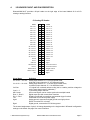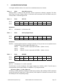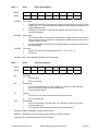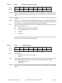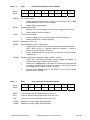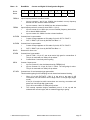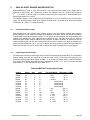
1
DIAMOND-MM-32-AT 16-Bit Analog I/O PC/104 Module with Autocalibration User Manual V2.64 Copyright 2003 Diamond Systems Corporation 8430-D Central Ave. Newark, CA 94560 Tel (510) 456-7800 Fax (510) 456-7878 [email protected] www.diamondsystems.com TABLE OF CONTENTS 1. DESCRIPTION........................................................................................................................................3 2. BLOCK DIAGRAM .................................................................................................................................4 3. BOARD CONFIGURATION DRAWING.................................................................................................5 4. I/O HEADER PINOUT AND PIN DESCRIPTION ...................................................................................6 5. BOARD CONFIGURATION....................................................................................................................8 6. I/O REGISTER MAP .............................................................................................................................11 7. I/O REGISTER DEFINITIONS ..............................................................................................................14 8. PAGE REGISTER DEFINITIONS.........................................................................................................23 9. ANALOG INPUT RANGES AND RESOLUTION.................................................................................26 10. PERFORMING AN A/D CONVERSION ...............................................................................................29 11. A/D SAMPLING METHODS .................................................................................................................31 12. HOW TO PERFORM A/D CONVERSIONS USING INTERRUPTS.....................................................33 13. ANALOG OUTPUT RANGES AND RESOLUTION.............................................................................35 14. GENERATING AN ANALOG OUTPUT ...............................................................................................36 15. AUTOCALIBRATION ...........................................................................................................................38 16. DIGITAL I/O OPERATION....................................................................................................................39 17. COUNTER/TIMER OPERATION..........................................................................................................43 18. SPECIFICATIONS ................................................................................................................................44 19. 82C54 COUNTER/TIMER DATASHEET .............................................................................................46 2003 Diamond Systems Corp. Diamond-MM-32-AT User Manual V2.64 Page 2 DIAMOND-MM-32-AT 1. PC/104 16-Bit Analog I/O Module with Autocalibration DESCRIPTION Diamond-MM-32-AT is a PC/104-format data acquisition board with a full set of features. It offers 32 total analog inputs with 16-bit resolution and programmable input range; 200,000 samples per second maximum sampling rate with FIFO operation; 4 analog outputs with 12-bit resolution; user-adjustable analog output ranges; 31 lines of digital I/O; one 32-bit counter/timer for A/D conversion and interrupt timing; and one 16-bit counter/timer for general purpose use. Diamond-MM-32-AT offers the additional important feature of autocalibration for both analog input and output channels. 1.1 Features Analog Inputs 32 input channels, may be configured as 32 single-ended, 16 differential, or 16 SE + 8 DI 16-bit resolution Programmable gain, range, and polarity on inputs 200,000 samples per second maximum sampling rate 512-sample FIFO for reduced interrupt overhead Autocalibration of all input ranges under software control Analog Outputs 4 analog output channels with 12-bit resolution, 5mA max output current Multiple fixed full-scale output ranges, including unipolar and bipolar ranges Programmable full-scale range capability Autocalibration under software control Digital I/O 24 bidirectional lines using integrated 8255-type circuit Buffered I/O for enhanced current drive Handshaking controls enable external latching of data as well as interrupt operation User-configurable pull-up / pull-down resistors 7 auxiliary I/O lines are fixed direction with programmable functions Counter/Timers and A/D Triggering 1 32-bit counter/timer for A/D pacer clock and interrupt operation timing 1 16-bit general purpose counter/timer Programmable input sources for each counter/timer External A/D triggering and gating inputs Multiple-board synchronization capability using A/D convert pulse out and external trigger in Interrupts may be generated by counter/timer Miscellaneous Extended temperature –40 to +85oC operation No trimpots or user adjustments required for calibration 2003 Diamond Systems Corp. Diamond-MM-32-AT User Manual V2.64 Page 3 2. BLOCK DIAGRAM 2003 Diamond Systems Corp. Diamond-MM-32-AT User Manual V2.64 Page 4 3. BOARD CONFIGURATION DRAWING Legend J1 PC/104 8-bit bus header J2 PC/104 16-bit bus header (only used for interrupt level) J3 Analog I/O header (includes trigger and ctr/timer signals) J4 Digital I/O header J5 Analog input single-ended / differential configuration J6 D/A unipolar / bipolar / full-scale range configuration J7 Base address / DMA level / interrupt level / bus width J8 Digital I/O pull-up / pull-down configuration J9 Test connector; not used in normal operation 2003 Diamond Systems Corp. Diamond-MM-32-AT User Manual V2.64 Page 5 4. I/O HEADER PINOUT AND PIN DESCRIPTION Diamond-MM-32-AT provides a 50-pin header on the right edge of the board labeled J3 for all I/O relating to analog functions. J3: Analog I/O Header AGND Vin 0 / 0+ Vin 1 / 1+ Vin 2 / 2+ Vin 3 / 3+ Vin 4 / 4+ Vin 5 / 5+ Vin 6 / 6+ Vin 7 / 7+ Vin 8 / 8+ Vin 9 / 9+ Vin 10 / 10+ Vin 11 / 11+ Vin 12 / 12+ Vin 13 / 13+ Vin 14 / 14+ Vin 15 / 15+ Vout 3 Vout 1 Vref Out A/D Convert Dout 1 Extclk / Din 3 Gate 0 / Din 1 +5V Signal Name Vin 15/15+ ~ Vin 0/0+ Vin 31/15- ~ Vin 16/0Vref Out Vout 0 - 3 AD Convert Dout 2 – Dout 0 Din 3 – Din 0 +5V Agnd Dgnd 1 3 5 7 9 11 13 15 17 19 21 23 25 27 29 31 33 35 37 39 41 43 45 47 49 2 4 6 8 10 12 14 16 18 20 22 24 26 28 30 32 34 36 38 40 42 44 46 48 50 AGND Vin 16 / 0Vin 17 / 1Vin 18 / 2Vin 19 / 3Vin 20 / 4Vin 21 / 5Vin 22 / 6Vin 23 / 7Vin 24 / 8Vin 25 / 9Vin 26 / 10Vin 27 / 11Vin 28 / 12Vin 29 / 13Vin 30 / 14Vin 31 / 15Vout 2 Vout 0 Agnd Ctr 2 Out / Dout 2 Ctr 0 Out / Dout 0 Extgate / Din 2 Clk 0 / Din 0 Dgnd Definition Analog input channels 15 - 0 in single-ended mode; High side of input channels 15 - 0 in differential mode Analog input channels 31 - 16 in both single-ended mode; Low side of input channels 15 - 0 in differential mode +5V signal from on-board reference chip (this is a stable, precision voltage but not the same signal used for calibration) 12-bit analog output channels A/D convert signal; can be used to synchronize multiple boards Digital output port with counter/timer functions Digital input port with counter/timer and external trigger functions Connected to PC/104 bus power supply Analog ground; connected to digital ground at a single point at DC/DC converter PS1 on board Digital ground; connected to PC/104 bus ground The channel assignments of pins 3-34 change depending on the single-ended / differential configuration settings on the board. See page 9 for more information. 2003 Diamond Systems Corp. Diamond-MM-32-AT User Manual V2.64 Page 6 Diamond-MM-32-AT provides a 34-pin header on the left edge of the board labeled J4 for the 24 8255type digital I/O lines. J4: Digital I/O Header A7 A5 A3 A1 B7 B5 B3 B1 C7 C5 C3 C1 Latch NC NC NC +5V Signal Name A7 – A0 B7 – B0 C7 – C0 Latch Ack +5V Dgnd 1 3 5 7 9 11 13 15 17 19 21 23 25 27 29 31 33 2 4 6 8 10 12 14 16 18 20 22 24 26 28 30 32 34 A6 A4 A2 A0 B6 B4 B2 B0 C6 C4 C2 C0 Ack NC NC NC Dgnd Definition Digital I/O port A Digital I/O port B Digital I/O port C Latch control input; active high Acknowledge output for interrupt-based I/O; active high Connected to PC/104 bus +5V power supply Digital ground; connected to PC/104 bus ground Note: In the documentation, CH refers to pins C7 – C4, while CL refers to pins C3 – C0. The operation of the Latch and Ack signals is described on page 41. 2003 Diamond Systems Corp. Diamond-MM-32-AT User Manual V2.64 Page 7 5. BOARD CONFIGURATION Refer to the Drawing of Diamond-MM-32-AT on page 5 for locations of the configuration items mentioned here. 5.1 Base Address Each board in the PC/104 system must have a different base address. Diamond-MM-32-AT's base address is set with 3 pairs of pins marked “ADDR” on pin header J7, located along the bottom of the board near the PC/104 bus connectors. The table below lists the 8 possible jumper configurations and the corresponding base addresses. Base Address Configuration Base Address Hex 140 340 100 180 200 280 300 380 5.2 Decimal 320 832 256 384 512 640 768 896 Pin Header J8 Configuration C Installed Installed Installed Installed Open Open Open Open B Installed Installed Open Open Installed Installed Open Open A Installed Open Installed Open Installed Open Installed Open Default Setting Interrupt level Interrupts are used for operations that are independent of normal program flow. Diamond-MM-32-AT can be set up to generate interrupts under several circumstances. The most common use of interrupts is to transfer A/D data from the board to system memory during high-speed A/D sampling. The board can also generate interrupts to transfer digital data into or out of the board, as well as at regular intervals according to a programmable timer on the board. Individual control bits are used to enable each type of interrupt. Jumper block J7 contains pins for selecting the interrupt level. To set the desired level, install a jumper under that level’s IRQ number and also in the R position. The R position connects a 1KΩ pull-down resistor to the selected IRQ line to allow the board to share the IRQ level with another board in the system. Note that only one pulldown resistor should be installed on any IRQ level. If you have another board in the system using the same IRQ level as Diamond-MM-32-AT, and that board has the pulldown resistor already configured, then remove the jumper from the R position on J7. 5.3 DMA level Jumper block J7 contains pins for selecting the DMA level. DMA is not currently supported on this board, but this feature is provided for potential future upgrades. These jumpers should be left in their default disconnected positions. On boards without FIFOs or memory buffers, DMA is required to support high-speed sampling at rates above the maximum sustainable interrupt rate (which is usually around 20,000 per second). However, DMM-32-AT contains a 512 sample FIFO that allows the interrupt rate to be much slower than the sample rate. The board can support full-speed sampling at up to 200,000 samples per second without the use of DMA. Therefore DMA is not currently supported in the software driver for this board. 2003 Diamond Systems Corp. Diamond-MM-32-AT User Manual V2.64 Page 8 5.4 Single-Ended / Differential A/D Channels The input channels on DMM-32-AT can be configured as 32 single-ended, 16 differential, or 16 singleended + 8 differential. Four different configurations are possible as described below. A single-ended input is a single-wire input that is measured with reference to the board’s analog ground. In order for the measurement to be accurate, the board’s ground must be at the same potential as the source signal’s ground. Usually this is accomplished by connecting the two grounds together at some point, for example by connecting to one of the analog ground pins on the I/O header J3. A differential input is a two-wire input that is measured by subtracting the low input from the high input. This type of connection offers two advantages: It allows for greater noise immunity, because the noise, which is present in equal amounts and equal phase on both the high and low inputs, is subtracted out when the low input is subtracted from the high input; and it allows for the signal to float away from ground. Normally the ground of the signal source is still connected to the ground on the A/D board in order to keep the signal from straying out of the common mode range of the A/D board’s input circuitry. To configure the input channels, set jumpers in jumper block J5 according to the table below. The corresponding channel numbering on the I/O header J3 is shown in drawings A-D (only the first 17 rows are shown; the remaining rows are the same as shown on page 6). A/D Channel Mode Configuration I/O Header Drawing 1 2 0-31 SE A In In Out Out Out Out 0-15 DI B Out Out In In In In 0-7 DI, 8-15 SE, 24-31 SE C Out In In Out In Out 0-7 SE, 8-15 DI, 16-23 SE D In Out Out In Out In Configuration A Agnd 0 1 2 3 4 5 6 7 8 9 10 11 12 13 14 15 1 2 3 4 5 6 7 8 9 10 11 12 13 14 15 16 17 18 19 20 21 22 23 24 25 26 27 28 29 30 31 32 33 34 35-50 Same as p. 6 B Agnd 16 17 18 19 20 21 22 23 24 25 26 27 28 29 30 31 Agnd 0+ 1+ 2+ 3+ 4+ 5+ 6+ 7+ 8+ 9+ 10+ 11+ 12+ 13+ 14+ 15+ 2003 Diamond Systems Corp. Jumper Settings 3 4 5 6 C 1 2 3 4 5 6 7 8 9 10 11 12 13 14 15 16 17 18 19 20 21 22 23 24 25 26 27 28 29 30 31 32 33 34 35-50 Same as p. 6 Agnd 0123456789101112131415- Agnd 0+ 1+ 2+ 3+ 4+ 5+ 6+ 7+ 8 9 10 11 12 13 14 15 1 2 3 4 5 6 7 8 9 10 11 12 13 14 15 16 17 18 19 20 21 22 23 24 25 26 27 28 29 30 31 32 33 34 35-50 Same as p. 6 D Agnd 0123456724 25 26 27 28 29 30 31 Diamond-MM-32-AT User Manual V2.64 Agnd 0 1 2 3 4 5 6 7 8+ 9+ 10+ 11+ 12+ 13+ 14+ 15+ 1 2 3 4 5 6 7 8 9 10 11 12 13 14 15 16 17 18 19 20 21 22 23 24 25 26 27 28 29 30 31 32 33 34 35-50 Same as p. 6 Agnd 16 17 18 19 20 21 22 23 89101112131415- Page 9 5.5 D/A Configuration The four analog outputs on DMM-32-AT can be set to operate in bipolar (both + and –) or unipolar (+ only) voltage ranges. In addition, the full-scale output range can be set to 5V, 10V, or programmable. On power up, the DACs can be configured to reset to mid-scale (0V in bipolar mode) or zero scale (0V in unipolar mode). In programmable mode, the full-scale output voltage can be set anywhere from 0V to 10V in software. You must use the Universal Driver software to set programmable D/A range, as it requires calibration to fine-tune the setting to the desired value. The Diamond-MM-32-AT demo program includes a section showing how to set the D/A range in software. To configure the analog output range, set jumper block J6 according to the tables below. The first four positions are used for the output range, and the 5th position is for the power up reset mode. J6: Analog Output Configuration A. Output range configuration Jumper Settings Output Range 10 5 P B R ±5V Out In Out In X ±10V 0-5V 0-10V Programmable, unipolar* Programmable, bipolar* In Out In Out Out Out In Out Out Out Out Out Out In In In Out Out Out In X X X X X * Programmable mode requires use of driver software to set and calibrate range. B. Power-up reset mode configuration Jumper Settings Reset Mode Mid-scale (Bipolar modes) Zero scale (Unipolar modes) 5.6 10 X X 5 X X P X X B X X R Out In Digital I/O Pull-Up / Pull-Down The 24 digital I/O lines on I/O header J4 are connected to 4.7K resistors that can be configured for either pull-up or pull-down. All resistors are configured in the same way. Jumper block J8 in the lower left corner of the board is used for configuration. To set the pull direction, install a jumper above the mark +5 or GND as desired. The +5 and Ground signals are wired to opposite corners of J8 to prevent accidentally shorting out the power supply by inserting the jumper incorrectly. 5.7 16-Bit Bus The board can be configured for 16-bit read operations when reading the A/D data. To do this, install a jumper in the “16” location on J7. A 16-bit read will only occur during a 16-bit read instruction from the base address (A/D data) when a jumper is in the “16” position and the board is in a 16-bit bus (both PC/104 J1 and J2 connectors are connected to the CPU). Otherwise the A/D board and host CPU will ignore the 16-bit setting and/or instruction and convert the 16-bit operation into two 8-bit read operations from base + 0 and base + 1. 2003 Diamond Systems Corp. Diamond-MM-32-AT User Manual V2.64 Page 10 6. I/O REGISTER MAP Diamond-MM-32-AT occupies 16 bytes in the system I/O address space. These registers are described in detail in the next chapter. Direct register access is not required if you are using the Universal Driver™ software that ships with the board. The driver handles all board access and provides a high-level set of functions to simplify programming. The information presented here and in the next chapter is intended to provide a detailed description of the board’s features and operation, as well as for programmers who are not using the Universal Driver software. Diamond-MM-32-AT I/O Register Map Base + 0 1 2 3 4 5 6 7 8 9 10 11 12* 13* 14* 15* Write Function Start A/D conversion Auxiliary digital output A/D low channel register A/D high channel register D/A LSB register D/A MSB + channel register FIFO depth register FIFO control register Miscellaneous control register Operation control register Counter/timer control register Analog configuration register 8254 / 8255 register 8254 / 8255 register 8254 / 8255 register 8254 / 8255 register Read Function A/D LSB (bits 7 - 0) A/D MSB (bits 15 - 8) A/D low channel register readback A/D high channel register readback Auxiliary digital input port Update all D/A channels FIFO depth register FIFO status register Status register Operation status register Counter/timer control reg. readback Analog configuration reg. readback 8254 / 8255 register 8254 / 8255 register 8254 / 8255 register 8254 / 8255 register See Page 14 14 15 15 15 16 17 18 19 20 21 22 23 23 23 23 * Registers 12 through 15 are paged in order to limit the number of I/O locations required for the board to 16. The Miscellaneous control register at Base + 8 is used to select the active page: Page 0 is the 8254 counter/timer access page. Page 1 is the 8255 digital I/O access page. Page 2 is reserved for future expansion. Page 3 is used for calibration operations and should not be accessed by the user under normal conditions. 2003 Diamond Systems Corp. Diamond-MM-32-AT User Manual V2.64 Page 11 WRITE Blank bits are unused and have no effect. 0 1 DOUT2 DOUT1 DOUT0 2 L4 L3 L2 L1 L0 3 H4 H3 H2 H1 H0 DA4 DA3 DA2 DA1 DA0 DA11 DA10 DA9 DA8 FD4 FD3 FD2 FD1 FIFOEN SCANEN FIFORST 4 DA7 DA6 5 DACH1 DACH0 6 FD8 FD7 DA5 FD6 FD5 7 8 RESETA RESETD INTRST P1 P0 CLKEN CLKSEL 9 ADINTE DINTE TINTE RSVD1 RSVD2 10 FREQ12 FREQ0 OUT2EN OUT0EN RSVD GT0EN SRC0 GT12EN SCINT1 SCINT0 RANGE ADBU G1 G0 11 READ Blank bits read back as 0. 0 AD7 AD6 AD5 AD4 AD3 AD2 AD1 AD0 1 AD15 AD14 AD13 AD12 AD11 AD10 AD9 AD8 2 L4 L3 L2 L1 L0 3 H4 H3 H2 H1 H0 DIN3 DIN2 DIN1 DIN0 4 DACBUSY CALBUSY 5 Update D/A 6 FD8 FD7 FD6 FD5 FD4 FD3 FD2 FD1 7 EF HF FF OVF FIFOEN SCANEN PAGE1 PAGE0 8 STS S/D1 S/D0 ADCH4 ADCH3 ADCH2 ADCH1 ADCH0 9 ADINT DINT TINT CLKEN CLKSEL 10 FREQ12 FREQ0 OUT2EN 11 WAIT RSVD OUT0EN RSVD GT0EN SRC0 GT12EN RANGE ADBU G1 G0 Registers 12-15 are paged registers. The definitions for these registers are described on the next page. 2003 Diamond Systems Corp. Diamond-MM-32-AT User Manual V2.64 Page 12 Page 0: 82C54 Counter/Timer Access These registers are described in the 82C54 datasheet appended to the back of this manual. Write 12 Ctr0D7 Ctr0D6 Ctr0D5 Ctr0D4 Ctr0D3 Ctr0D2 Ctr0D1 Ctr0D0 13 Ctr1D7 Ctr1D6 Ctr1D5 Ctr1D4 Ctr1D3 Ctr1D2 Ctr1D1 Ctr1D0 14 Ctr2D7 Ctr2D6 Ctr2D5 Ctr2D4 Ctr2D3 Ctr2D2 Ctr2D1 Ctr2D0 15 SC1 SC0 RW1 RW0 M2 M1 M0 BCD Ctr0D6 Ctr0D5 Ctr0D4 Ctr0D3 Ctr0D2 Ctr0D1 Ctr0D0 Read 12 Ctr0D7 13 Ctr1D7 Ctr1D6 Ctr1D5 Ctr1D4 Ctr1D3 Ctr1D2 Ctr1D1 Ctr1D0 14 Ctr2D7 Ctr2D6 Ctr2D5 Ctr2D4 Ctr2D3 Ctr2D2 Ctr2D1 Ctr2D0 15 SC1 SC0 RW1 RW0 M2 M1 M0 BCD Page 1: 82C55-Type Digital I/O Write 12 A7 A6 A5 A4 A3 A2 A1 A0 13 B7 B6 B5 B4 B3 B2 B1 B0 14 C7 C6 C5 C4 C3 C2 C1 C0 15 1 ModeC ModeA DIRA DIRCH ModeB DIRB DIRCL A7 A6 A5 A4 A3 A2 A1 A0 13 B7 B6 B5 B4 B3 B2 B1 B0 14 C7 C6 C5 C4 C3 C2 C1 C0 15 1 ModeC ModeA DIRA DIRCH ModeB DIRB DIRCL Read 12 Page 2: Auxiliary Control (FPGA revision code 35 and higher only) Write/Read 15 CTEDGE Page 3: Autocalibration Registers Write 12 D7 13 D6 D5 D4 D3 D2 D1 D0 A6 A5 S4 A3 A2 A1 A0 14 EE_EN EE_RW RUNCAL CMUXEN TDACEN 15 1 0 1 0 0 1 0 1 D7 D6 D5 D4 D3 D2 D1 D0 A6 A5 S4 A3 A2 A1 A0 TDBUSY EEBUSY CMUXEN TDACEN 0 0 0 Read 12 13 14 0 15 2003 Diamond Systems Corp. FPGA Revision Code Diamond-MM-32-AT User Manual V2.64 Page 13 7. I/O REGISTER DEFINITIONS In all register definitions below, a bit named X is not defined and serves no function. Base + 0 Write Start A/D Conversion Writing to Base + 0 starts an A/D conversion, unless a conversion is already in progress. The value written does not matter. Writing to Base + 0 will start an A/D conversion even if the board is set up for interrupt, DMA, or external trigger mode. Base + 0 Read A/D LSB Bit No. 7 6 5 4 3 2 1 0 Name AD7 AD6 AD5 AD4 AD3 AD2 AD1 AD0 Definitions: AD7 - 0 Base + 1 A/D data bits 7 - 0; AD0 is the LSB Write Auxiliary Digital Output Bit No. 7 6 5 4 3 2 1 0 Name X X X X X DOUT2 DOUT1 DOUT0 Definitions: DOUT2-0 Base + 1 Auxiliary digital output bits on analog I/O header J3. Two pins also serve as optional counter outputs based on control register bits at Base + 10: DOUT2 J3 pin 42. Counter 2 output when OUT2EN = 1 (Base + 10 bit 5). DOUT1 J3 pin 43 DOUT0 J3 pin 44. Counter 0 output when OUT0EN = 1 (Base + 10 bit 4). Read A/D MSB Bit No. 7 6 5 4 3 2 1 0 Name AD15 AD14 AD13 AD12 AD11 AD10 AD9 AD8 Definitions: AD15 - 8 A/D data bits 15 - 8; AD15 is the MSB The A/D value is a twos complement 16-bit integer ranging from -32768 to +32767. The A/D value is constructed from the two bytes at Base + 0 and Base + 1 by using the formula: A/D value = (Base + 1) * 256 + (Base + 0) A reading of -32768 represents a negative full scale input (or below), and a reading of 32767 represents an input of positive full scale minus 1 LSB (or above). See Chapter 9 for formulas to convert the 16-bit A/D reading into the corresponding voltage. 2003 Diamond Systems Corp. Diamond-MM-32-AT User Manual V2.64 Page 14 Base + 2 Read/Write A/D Low Channel Register Bit No. 7 6 5 4 3 2 1 0 Name X X X L4 L3 L2 L1 L0 Definitions: L4-0 Base + 3 The low channel number setting in the A/D channel scan range. Channel numbers range from 0 to 31 in single-ended mode. Read/Write A/D High Channel Register Bit No. 7 6 5 4 3 2 1 0 Name X X X H4 H3 H2 H1 H0 Definitions: H4-0 Base + 4 The high channel number setting in the A/D channel scan range. Channel numbers range from 0 to 31 in single-ended mode. Write DAC LSB Bit No. 7 6 5 4 3 2 1 0 Name DA7 DA6 DA5 DA4 DA3 DA2 DA1 DA0 Definitions: DA7 - 0 D/A data bits 7 - 0 for the channel currently being accessed. This register is a holding register. Writing to it does not affect any D/A channel until the MSB is written. When the MSB is written (see below, Base + 5), the value written to that register, along with the value written to this register, are simultaneously written to the D/A chip’s load register for the selected channel. See the instructions under “Base + 5, Read” on the next page for updating the D/A after the data has been written. 2003 Diamond Systems Corp. Diamond-MM-32-AT User Manual V2.64 Page 15 Base + 4 Read Bit No. Name Status / Auxiliary digital inputs 7 6 DACBUSY CALBUSY 5 4 3 2 1 0 X X DIN3 DIN2 DIN1 DIN0 Definitions: DIN3-0 Auxiliary digital inputs on analog I/O header J3. These pins have multiple functions based on control bits at Base + 9 and Base + 10: DIN3 J3 pin 45. External A/D clock when CLKSEL = 1 (Base + 9 bit 0) DIN2 J3 pin 46. Gate for counters 1 and 2 when GT12EN = 1 (Base + 10 bit 0) DIN1 J3 pin 47. Gate for counter 0 when GT0EN = 1 (Base + 10 bit 2) DIN0 J3 pin 48. Clock for counter 0 when SRC0 = 1 (Base + 10 bit1) DACBUSY D/A serial data transfer is in progress. DACBUSY = 1 for 10uS after writing to base + 5. Do not attempt to write to the D/A converter at bass + 4 or base + 5 while this bit is high. This bit must be checked before any write to these registers. CALBUSY Calibration is in progress or EEPROM is being accessed. Do not attempt calibration or EEPROM access while this bit is high. This bit must be checked before any calibration or EEPROM operation is attempted. Base + 5 Write DAC MSB + Channel No. Bit No. 7 6 5 4 3 2 1 0 Name DACH1 DACH0 X X DA11 DA10 DA9 DA8 Definitions: DACH1-0 Binary number of the D/A channel, 3 - 0 DA11 - 8 D/A bits 11 - 8 for the selected output channel; DA11 is the MSB See the instructions below for updating the D/A after the data has been written. Base + 5 Read Update D/A Channel Reading from this address causes the most recently-written D/A channel to update with its new value. DMM-32-AT does not support simultaneous update of D/A channels, as the D/A chip has only one internal data register. Each D/A channel must be updated independently before the next one’s data is written. Writing to a D/A requires four steps: 1. Write the LSB to base + 4 2. Write the MSB and channel no. to base + 5 3. Monitor the DACBUSY bit until it is 0, indicating the data has been loaded into the chip. 4. Read from base + 5 to update the D/A chip After updating the D/A, you may immediately resume writing data to Base + 4 / Base + 5 to update another channel if desired. 2003 Diamond Systems Corp. Diamond-MM-32-AT User Manual V2.64 Page 16 Base + 6 Read / Write FIFO Depth Register Bit No. 7 6 5 4 3 2 1 0 Name FD8 FD7 FD6 FD5 FD4 FD3 FD2 FD1 FD8-1 FIFO threshold. This is the level at which the board will generate an interrupt request when the FIFO is enabled (FIFOEN = 1 in base + 7). Note that the value written is shifted by 1 bit, i.e. divided by 2. For example, if you want a FIFO threshold of 256 samples, write a 128 to this register. The reason for this shift is that the FIFO size is 512 samples, so to cover the entire range of FIFO thresholds the value needs to be shifted. The interrupt routine must read exactly this number of samples out each time it runs. The last time the routine runs, it should read whatever is remaining in the FIFO by monitoring the EF bit (Empty Flag) in the FIFO status register at base + 7. When the FIFO is empty, EF = 1, and the FIFO returns the value hex FF on all read operations. The DSC Universal Driver uses a default threshold of 256 for all operations, but this value can be overwritten using the function parameters. If you are sampling at a slow rate or want to control when the interrupt occurs, you can set the threshold to a low value. For example, if you are sampling 16 channels at 10Hz and you want an interrupt each set of samples, you can set the threshold to 16 (write an 8 to this register), so that an interrupt will occur each 16 samples. Then the interrupt routine should read out 16 samples from the FIFO, and you get new data as soon as it is available. For higher sample rates (100KHz or higher) it may be necessary to increase the threshold above 256, to around 350. If you set the threshold too high, you may overrun the FIFO, since the interrupt routine may not respond before the remaining locations are filled, causing an overflow. An overflow can be detected by checking the OVF bit in the FIFO status register at Base + 7. The correct threshold for your application can only be determined by testing. 2003 Diamond Systems Corp. Diamond-MM-32-AT User Manual V2.64 Page 17 Base + 7 Write FIFO Control Register Bit No. 7 6 5 4 Name X X X X 3 2 1 0 FIFOEN SCANEN FIFORST X FIFOEN FIFO enable: 1 Enable FIFO operation; if interrupts are enabled, interrupts will occur when the FIFO is half full (HF = 1). This slows down the interrupt rate dramatically compared to the actual A/D sample rate. 0 Disable FIFO operation; if interrupts are enabled, interrupts will occur after each A/D conversion. SCANEN Scan enable: 1 Scan mode enabled; FIFO will fill up with data for a single scan, and STS will stay high until entire scan is complete; if interrupts are enabled, interrupts will occur on integral multiples of scans. 0 Scan mode disabled; The STS bit will correspond directly to the status indicator from the A/D converter FIFORST FIFO reset: 1 Reset FIFO; after this command is issued, EF = 1, HF = 0, FF = 0 0 No function See page 32 for a more detailed description of FIFO operation. Base + 7 Read FIFO Status Register Bit No. 7 6 5 4 Name EF HF FF OVF 3 2 1 FIFOEN SCANEN PAGE1 0 PAGE0 EF Empty flag: 1 FIFO is empty 0 FIFO is not empty HF Half full flag: 1 FIFO is at least half full; The FIFO contains 512 words, so if this flag is set the FIFO contains at least 256 words of A/D data 0 FIFO is less than half full FF Full flag: 1 FIFO is full; the next A/D conversion will result in an overflow 0 FIFO is less than full OVF Overflow flag: 1 FIFO has overflowed; data has been lost. This flag is cleared on the next successful A/D read. 0 FIFO has not overflowed since the last time A/D data was read FIFOEN, SCANEN Readback of control bits from above PAGE1-0 Readback of the current page register setting; see Base + 8 below See page for a complete description of FIFO operation. 2003 Diamond Systems Corp. Diamond-MM-32-AT User Manual V2.64 Page 18 Base + 8 Write Miscellaneous Control Register Bit No. 7 6 Name X X 5 4 3 RESETA RESETD INTRST 2 1 0 X P1 P0 RESETA Writing a 1 to this bit causes a full reset of all features of the board, including the DACs, the FIFO, the digital I/O, and all internal registers. The counter/timers are not affected by this reset. RESETD Writing a 1 to this bit causes a reset identical to above except the analog outputs are not affected. INTRST Writing a 1 to this location resets the interrupt request circuit on the board. The programmer must write a 1 to this bit during the interrupt service routine, or further interrupts will not occur. Writing a 1 to this bit does not disturb the values of the PAGE bits. P1-0 Two-bit value that selects which I/O device is accessible through the registers at locations Base + 12 through base + 15: 00 8254 type counter/timer device is accessible 01 8255 type digital I/O device is accessible 10 Reserved 11 Calibration Writing to the page bits will not generate a board reset or interrupt reset, as long as those bits are kept at 0 in the data written to this register. Base + 8 Read A/D Status Register Bit No. 7 6 5 4 3 2 1 0 Name STS S/D1 S/D0 ADCH4 ADCH3 ADCH2 ADCH1 ADCH0 STS A/D chip status: 1 A/D conversion or A/D scan in progress 0 A/D idle S/D1-0 Single-ended / Differential A/D input mode indicator. S/D1 controls the channels 8-15 and 24-31, S/D0 controls 0-7 and 16-23. See page for A/D channel configuration settings. 1 Single-ended (default) 0 Differential ADCH4-0 Current A/D channel; this is the channel currently selected on board and is the channel that will be used for the next A/D conversion (unless a new value is written to the channel register). 2003 Diamond Systems Corp. Diamond-MM-32-AT User Manual V2.64 Page 19 Base + 9 Write Interrupt and A/D Clock Control Register Bit No. 7 6 5 4 3 2 Name ADINTE DINTE TINTE RSVD1 RSVD2 X 1 0 CLKEN CLKSEL ADINTE A/D interrupt enable: 1 Analog interrupt; interrupts occur according to the settings of the FIFOEN and SCANEN bits in the FIFO control register 0 Disable A/D interrupt operation DINTE Digital interrupt enable: 1 Interrupts occur on rising edges of the Latch pin on Digital I/O header J4. 0 Disable digital I/O interrupt operation TINTE Timer 0 interrupt enable: 1 Interrupt requests occur on the falling edge of 82C54 counter/timer 0 0 Disable counter/timer 0 interrupt operation RSVD1-2 Reserved for future use CLKEN Enable hardware clock for A/D sampling: 1 Enable hardware clock for A/D (source is selected with CLKSEL bit below); NOTE: When this bit is 1, software triggers are disabled, i.e. writing to base+0 will not start an A/D conversion. 0 Disable hardware clocking for A/D; A/D conversions occur with software command only CLKSEL Hardware clock select (enabled only when CLKEN = 1 above): NOTE: When this feature is selected, software triggers are disabled, i.e. writing to base+0 will not start an A/D conversion. 1 Internal clock: Falling edges on the output of counter/timer 2 generate A/D conversions. Counter 2 is in turn driven by counter 1, which is driven by the clock selected by bit FREQ12 in Base + 10 below. 0 External trigger: Falling edges on the EXTCLK pin on the I/O header generate A/D conversions. Base + 9 Read Interrupt and A/D Clock Status Register Bit No. 7 6 5 4 3 2 Name ADINT DINT TINT X X X ADINT 1 when an A/D interrupt request has occurred, else 0 DINT 1 when a digital I/O interrupt request has occurred, else 0 TINT 1 when a timer interrupt request has occurred, else 0 CLKEN Readback of control register bit defined above CLKSEL Readback of control register bit defined above 2003 Diamond Systems Corp. Diamond-MM-32-AT User Manual V2.64 1 0 CLKEN CLKSEL Page 20 Base + 10 Read/Write Bit No. 7 Counter and Digital I/O Configuration Register 6 5 4 3 2 1 0 RSVD GT0EN SRC0 GT12EN Name FREQ12 FREQ0 OUT2EN OUT0EN FREQ12 Input frequency select for counters 1 and 2: 1 Input to counters 1 and 2 is a 100KHz (one hundred, not ten) frequency derived from the on-board 10MHz oscillator 0 Input to counters 1 and 2 is 10MHz from the on-board oscillator FREQ0 Input frequency select for counter 0 when SRC0 = 1 (bit 1): 1 Input to counter 0 is a 10KHz (ten, not one hundred) frequency derived from the on-board 10MHz oscillator 0 Input to counter 0 is 10MHz from the on-board oscillator OUT2EN Counter/timer 2 output enable: 1 Counter 2 output appears on I/O header J3 pin 42, OUT 2 / DOUT 2 0 OUT 2 / DOUT 2 pin is set by bit DOUT2 at Base + 1 OUT0EN Counter/timer 0 output enable: 1 Counter 0 output appears on I/O header J3 pin 44, OUT 0 / DOUT 0 0 OUT 0 / DOUT 0 pin is set by bit DOUT0 at Base + 1 RSVD Reserved for future use GT0EN Counter/timer 0 gate enable: 1 Gate 0 / DIN 1, J3 pin 47, acts as an active high gate for counter/timer 0. This pin is connected to a 10KΩ pull-up resistor. 0 Counter/timer 0 runs freely with no gating SRC0 Counter 0 input source: 1 Input to Counter 0 is the clock determined by FREQ0 (bit 6) 0 Input to Counter 0 is J3 pin 48, CLK 0 / DIN 0. The rising edge is active. This pin is connected to a 10KΩ pull-up resistor. GT12EN Counter/timer 1/2 and external trigger gate enable: This bit enables gating for A/D sampling for both internal and external clocking. 1 When J3 pin 46 (EXTGATE / DIN 2) is low prior to the start of A/D conversions, A/D conversions will not begin until it is brought high (trigger mode). If the pin is brought low while conversions are occurring, conversions will pause until it is brought high (gate mode). 0 J3 pin 46 is connected to a 10KΩ pull-up resistor. The interrupt operation begins immediately once it is set up and the selected clock source begins, with no external triggering or gating. 2003 Diamond Systems Corp. Diamond-MM-32-AT User Manual V2.64 Page 21 Base + 11 Write Analog Configuration Register Bit No. 7 6 Name X X 5 4 3 SCINT1 SCINT0 RANGE 2 1 0 ADBU G1 G0 This register controls the analog input range for all channels on the board. See the gain/range setting table on page 26 for a complete list of valid settings and corresponding input ranges for these 4 bits. SCINT1-0 Scan interval. This is the time between A/D samples when performing a scan (SCANEN = 1). The driver sets a default of 20uS. SCINT1 SCINT0 0 0 0 1 1 0 1 1 Interval 20µS 15µS 10µS 5µS RANGE 5V or 10V A/D positive full-scale voltage ADBU A/D bipolar / unipolar setting; 0 = bipolar, 1 = unipolar The table below lists the effects of the various combinations of ADBU and RANGE: RANGE 0 0 1 1 G1 - 0 ADBU 0 1 0 1 A/D full-scale range ±5V Invalid setting ±10V 0 - 10V A/D programmable gain amplifier setting: G1 0 0 1 1 G0 0 1 0 1 Gain 1 2 4 8 The gain setting is the ratio between the A/D full-scale range and the effective input signal range. For example, if the A/D full-scale range is 0 - 10V, a gain setting of 2 creates an input signal range of 0 - 5V, and a gain setting of 4 creates an input signal range of 0 - 2.5V. ⇒: On power up or system reset, the board is configured for A/D bipolar mode, input range = ±5V, and gain = 1, corresponding to all zeroes in this register. Base + 11 Read Bit No. 7 6 5 4 3 2 1 0 Name WAIT RSVD X X RANGE ADBU G1 G0 WAIT Analog I/O Readback Register Analog input circuit settling time holdoff indicator: 1 The analog input circuit is settling on a new signal and is not yet ready for a new conversion to start; this will occur each time you change the channel, gain, or input range on the board. The wait time is approximately 10µS. 0 The analog input circuit has settled, and a new A/D conversion may begin RANGE, ADBU, G1, G0 Readback of control bits described above 2003 Diamond Systems Corp. Diamond-MM-32-AT User Manual V2.64 Page 22 8. PAGE REGISTER DEFINITIONS Registers 12 through 15 are paged to support multiple functions. The page control bits are located in Base + 8. The pages are defined as: 0 1 2 3 82C54 counter/timer is accessible 82C55-type digital I/O circuit is accessible Reserved Calibration control Pages 0, and 1 are defined below. Page 2 is reserved for future expansion. Page 3 is reserved for autocalibration operation. 8.1 Page 0: 82C54 Counter/Timer Access Base + 12 ~ Base + 15 Read/Write When page 0 is selected, these 4 registers map directly to the 82C54 counter/timer chip on the board. Base + 12 maps into register 0 of the 82C54, defined as A1 = 0 and A0 = 0 in the 82C54 datasheet, and so on. A copy of the 82C54 datasheet is supplied in the appendix to this manual. 8.2 Page 1: 82C55 Digital I/O Circuit Base + 12 ~ Base + 15 Read/Write When page 1 is selected, these registers map directly to the internal 82C55-type digital I/O circuit. The system controller chip on DMM-32-AT contains a partial implementation of an 82C55 24-line digital I/O chip. Currently only Mode 0 (direct I/O) is defined, along with enhancements for data latching and acknowledge signals. The behavior of this digital I/O port is described in Chapter 15. 8.3 Page 2: Auxiliary Control (FPGA revision code 35 and higher only) This page contains one control bit used to determine the active edge for counter-based interrupts. Base + 15 Bit No. Read/Write 7 Auxiliary Control 6 5 4 3 2 Name CTEDGE 1 0 CTEDGE Determines which edge of the 82C54 counter 0 output signal will generate an interrupt when counter interrupts are enabled. This bit affects only counter 0, not counters 1 and 2. 0 = rising edge, 1 = falling edge The 82C54 counters can be programmed in 6 modes to suit a variety of applications. In modes 0 and 1, the counter output is initially low, then times out with a rising edge. In modes 4 and 5, the counter output is high, then times out with a falling edge. This register bit is used to select the appropriate active edge, so that the counter timeout event will generate an interrupt. 2003 Diamond Systems Corp. Diamond-MM-32-AT User Manual V2.64 Page 23 8.4 Page 3: Autocalibration Registers When page 3 is selected, the calibration registers are accessible. These registers are used to access the TrimDAC and EEPROM used in the calibration process. Base + 12 Read/Write EEPROM / TrimDAC Data Register Bit No. 7 6 5 4 3 2 1 0 Name D7 D6 D5 D4 D3 D2 D1 D0 D7-0 Calibration data to be read or written to the EEPROM and/or TrimDAC. During EEPROM or TrimDAC write operations, the data written to this register will be written to the selected device. During EEPROM read operations this register contains the data to be read from the EEPROM and is valid after EEBUSY = 0. The TrimDAC data cannot be read back. Base + 13 Read/Write EEPROM / TrimDAC Address Register Bit No. 7 6 5 4 3 2 1 0 Name X A6 A5 A4 A3 A2 A1 A0 A6-A0 EEPROM / TrimDAC address. The EEPROM recognizes address 0 – 127 using address bits A6 – A0. The TrimDAC only recognizes addresses 0 – 7 using bits A2 – A0. In each case remaining address bits will be ignored. 2003 Diamond Systems Corp. Diamond-MM-32-AT User Manual V2.64 Page 24 Base + 14 Write Bit No. 7 Name EE_EN Calibration Control Register 6 5 4 3 EE_RW RUNCAL CMUXEN TDACEN 2 1 0 X X X This register is used to initiate various commands related to autocalibration. More detailed information on autocalibration may be found elsewhere in this manual. EE_EN EEPROM Enable. Writing a 1 to this bit will initiate a transfer to/from the EEPROM as indicated by the EE_RW bit. EE_RW Selects read or write operation for the EEPROM: 0 = Write, 1 = Read. RUNCAL Writing 1 to this bit causes the board to reload the calibration settings from EEPROM. CMUXEN Calibration multiplexor enable. The cal mux is used to read precision on-board reference voltages that are used in the autocalibration process. It also can be used to read back the value of analog output 0. 1 = enable cal mux and disable user analog input channels 0 = disable cal mux, enable user inputs TDACEN TrimDAC Enable. Writing 1 to this bit will initiate a transfer to the TrimDAC (used in the autocalibration process). Base + 14 Read Bit No. 7 Name 0 Calibration Status Register 6 5 4 TDBUSY EEBUSY CMUXEN TDACEN TDBUSY TrimDAC busy indicator 0 User may access TrimDAC 1 TrimDAC is being accessed; user must wait EEBUSY EEPROM busy indicator 0 User may access EEPROM 1 EEPROM is being accessed; user must wait Base + 15 3 Write 2 1 0 0 0 0 EEPROM Access Key Register The user must write the value 0xA5 (binary 10100101) to this register each time after setting the PAGE bit in order to get access to the EEPROM. This helps prevent accidental corruption of the EEPROM contents. Base + 15 Read FPGA Revision Code This register may be read back to indicate the revision level of the board’s controller FPGA design. All features described in this chapter are available on all revisions, except Page 2, which is available only on boards with revision code 35 and higher. If you have technical support issues, please determine the FPGA revision of your board before contacting technical support. 2003 Diamond Systems Corp. Diamond-MM-32-AT User Manual V2.64 Page 25 9. ANALOG INPUT RANGES AND RESOLUTION Diamond-MM-32-AT uses a 16-bit A/D converter. This means that the analog input voltage can be measured to the precision of a 16-bit binary number. The maximum value of a 16-bit binary number is 216 - 1, or 65535, so the full range of numerical values that you can get from a Diamond-MM-32-AT analog input channel is 0 - 65535. The smallest change in input voltage that can be detected is 1/(216), or 1/65536, of the full-scale input range. This smallest change results in an increase or decrease of 1 in the A/D code, and so this change is referred to as 1 LSB, or 1 least significant bit. 9.1 Unipolar and Bipolar Inputs Diamond-MM-32-AT can measure both unipolar (positive only) and bipolar (positive and negative) analog voltages. The full-scale input voltage range depends on the Gain, Range, and Polarity bit settings in the Analog Configuration Register at base + 11. In front of the A/D converter is a programmable gain amplifier that multiplies the input signal before it reaches the A/D. This gain circuit has the effect of scaling the input voltage range to match the A/D converter for better resolution. In general you should select the highest gain you can that will allow the A/D converter to read the full range of voltages over which your input signals will vary. If you pick too high a gain, then the A/D converter will clip at either the high end or low end, and you will not be able to read the full range of voltages on your input signals. 9.2 Input Ranges and Resolution The table below lists the full-scale input range for each valid analog input configuration. The parameters Polarity, Range, and Gain are combined to create the value “Code”, which is the value that you must write to the analog configuration register at Base + 11 to get the input range shown. A total of 9 different input ranges are possible. Note that the range programming codes 4, 5, 6, and 7 are invalid and that range codes 9 – 11 are equivalent to range codes 0 – 2. Diamond-MM-32-AT Analog Input Ranges Polarity Bipolar Bipolar Bipolar Bipolar Unipolar Unipolar Unipolar Unipolar Bipolar Bipolar Bipolar Bipolar Unipolar Unipolar Unipolar Unipolar Range 5V 5V 5V 5V 5V 5V 5V 5V 10V 10V 10V 10V 10V 10V 10V 10V 2003 Diamond Systems Corp. Gain 1 2 4 8 1 2 4 8 1 2 4 8 1 2 4 8 Code 0 1 2 3 4 5 6 7 8 9 10 11 12 13 14 15 Full-Scale Range Resolution (1 LSB) ±5V 153 µV ±2.5V 76 µV ±1.25V 38 µV ±0.625V 19 µV Invalid setting Invalid setting Invalid setting Invalid setting ±10V 305 µV ±5V 153 µV ±2.5V 76 µV ±1.25V 38 µV 0 - 10V 153 µV 0 - 5V 76 µV 0 - 2.5V 38 µV 0 - 1.25V 19 µV Diamond-MM-32-AT User Manual V2.64 Page 26 9.3 A/D Conversion Formulas The 16-bit value returned by the A/D converter is always a twos complement number ranging from 32768 to 32767, regardless of the input range. This is because the input range of the A/D is fixed at ±10V. The input signal is actually magnified and shifted to match this range before it reaches the A/D. For example, for an input range of 0-10V, the signal is first shifted down by 5V to ±5V and then amplified by 2 to become ±10V. Therefore, two different formulas are needed to convert the A/D value back to a voltage, one for bipolar ranges, and one for unipolar ranges. Tables showing the correlation between A/D code and input voltage are shown on the following page. For Bipolar Input Ranges FS = full-scale voltage (e.g. 5V for ±5V range) If using a 16-bit signed integer in C: Input voltage = (A/D code / 32768) x FS Example: ±5V range selected, A/D code = 17762 (Hex 4560) Input voltage = (17762 / 32768) x 5V = +2.7103V Example: ±5V range selected, A/D code = -15008 (Hex C560) Input voltage = (-15008 / 32768) x 5V = -2.2900V If using a 32-bit signed integer in C, or unsigned or floating value in C or Basic: Input voltage = (A/D code / 32768) x FS If input voltage >= FS then input voltage = input voltage - 2 x FS Example: ±5V range selected, A/D code = 17762 (Hex 4560) Input voltage = (17762 / 32768) x 5V = +2.7103V Example: ±5V range selected, A/D code = 50528 (Hex C560) Input voltage = (50528 / 32768) x 5V = +7.7100V Since 7.7100V >= 5V, we must subtract: Input voltage = 7.7100V - 2 x 5V = -2.2900V For Unipolar Input Ranges FS = full-scale voltage (e.g. 10 for 0 - 10V range) Input voltage = ((A/D code + 32768) / 65536) x FS Example: 0 - 10V range selected, A/D code = 17762 (Hex 4560) Input voltage = ((17762 + 32768) / 65536) x 10V = +7.7103V Note that this is simply the result for the ±5V range shifted up by 5V. 2003 Diamond Systems Corp. Diamond-MM-32-AT User Manual V2.64 Page 27 9.4 Correlation between A/D Code and Input Voltage The two tables below illustrate the correlation between the A/D code and the corresponding input voltage. Use these tables as guides to help think about how to convert between the voltage domain and the A/D code domain. Bipolar Input Ranges A/D Code -32768 -32767 -1 0 1 32767 Input voltage formula -VFS -VFS + 1 LSB -1 LSB 0V +1 LSB VFS - 1 LSB Input voltage (±5V range) -5.0000V -4.9998V -0.153mV 0.0000V 0.153mV 4.9998V Unipolar Input Ranges A/D Code -32768 -32767 -1 0 1 32767 Input voltage formula 0V 1 LSB (VFS / 65536) VFS / 2 - 1 LSB VFS / 2 VFS / 2 + 1 LSB VFS - 1 LSB 2003 Diamond Systems Corp. Input voltage (0 - 10V range) 0.0000V 0.153mV 4.99985V 5.0000V 5.00015V 9.9998V Diamond-MM-32-AT User Manual V2.64 Page 28 10. PERFORMING AN A/D CONVERSION This chapter describes the steps involved in performing an A/D conversion on a selected input channel using direct programming (not with the driver software). The A/D FIFO All A/D conversions are stored in an on-board FIFO (first in first out memory). The FIFO can hold up to 512 samples. Each time an A/D conversion is finished, the data is stored in the FIFO, and the FIFO counter increments by 1. Each time you read A/D data, you are actually reading it out of the FIFO, and the FIFO counter decrements by 1. When the FIFO is empty the data read from it is undefined – you may continue to read the last sample, or you may read all 1s. You can read each A/D sample as soon as it is ready, or you can wait until you take a collection of samples (up to 512 maximum) and then read them all out at once. To be sure that you are getting only current A/D data, be sure to reset the FIFO each time before you start any A/D operation. This will prevent errors caused by leaving data in from a previous operation. To reset the FIFO, write a 1 to bit 2 of register 7 (see page 18). This bit is not a real register bit; instead it triggers a command in the board’s controller chip. Therefore you do not need to write a 1 and then a 0, just write a 1. However writing to the FIFORST bit affects the values of other bits in this register as well: outp(base+7, 0x02); // this resets the FIFO and clears FIFOEN and SCANEN outp(base+7, 0x0A); // this resets the FIFO and SCANEN but leaves FIFOEN set Note that this register also contains a FIFO enable bit, FIFOEN. This bit only has meaning during A/D interrupt operations. The FIFO is always enabled and is always in use during A/D conversions. There are seven steps involved in performing an A/D conversion: 1. Select the input channel or input channel range 2. Select the analog input range (Range, Polarity, and Gain codes) 3. Wait for analog input circuit to settle 4. Start an A/D conversion on the current channel 5. Wait for the conversion to finish 6. Read the A/D data 7. Convert the numerical data to a meaningful value If you are going to sample the same channel multiple times or sample multiple consecutive channels with the same input range, you only need to perform steps 1-3 once, and then you can repeat steps 4-6 or 47 as many times as desired. 10.1 Select the input channel or input channel range Diamond-MM-32-AT contains a channel counter circuit that controls which channel will be sampled on each A/D conversion command. The circuit uses two channel numbers called the low channel and high channel. These are stored in registers at Base + 2 and Base + 3 (see page 15). The circuit starts at the low channel and automatically increments after each A/D conversion until the high channel is reached. When an A/D conversion is performed on the high channel, the circuit resets to the low channel and starts over again. This behavior enables you simplify your software by setting the channel range just once. To read continuously from a single channel, write the same channel number to both the low channel and high channel registers. To read from a series of consecutively numbered channels, write the starting channel to Base + 2 and the ending channel to Base + 3. To read from a group of non-consecutive channels, you must treat each as a single channel described above. 2003 Diamond Systems Corp. Diamond-MM-32-AT User Manual V2.64 Page 29 10.2 Select the analog input range Select the code from page 26 corresponding to the desired input range and write it to the analog I/O control register at Base + 11. You only need to write to this register if you want to select a different input range from the one used for the previous conversion. If all channels will be using the same input range, you can configure this register just once at the beginning of your procedure. You can read the current value of this register by reading from Base + 11. 10.3 Wait for the analog circuit to settle After changing either the input channel or the input range, you must allow the circuit to settle on the new value before performing an A/D conversion. The settling time is long compared to software execution times, so a timer is provided on board to indicate when it is safe to proceed with A/D sampling. The WAIT bit at base + 11 (see page 22) indicates when the circuit is settling and when it is safe to sample the input. When WAIT is 1 the board is settling; when WAIT is 0 the board is ready for an A/D conversion. 10.4 Start an A/D conversion on the current channel To generate an A/D conversion, simply write to base + 0 to start the conversion. The value you write does not matter and is ignored. 10.5 Wait for the conversion to finish The A/D converter takes about 4 microseconds to complete a conversion. If you try to read the A/D converter data immediately after starting a conversion, you will get invalid data. Therefore the A/D converter provides a status signal to indicate whether it is busy or idle. This signal can be read back as the STS bit in the status register at base + 8 (see page 19). When the A/D converter is busy (performing an A/D conversion), this bit is 1, and when the A/D converter is idle (conversion is done and data is available), this bit is 0. 10.6 Read the A/D data Once the conversion is complete, you can read the data back from the A/D converter. The data is 16 bits wide and is read back in two 8-bit bytes at Base + 0 and Base + 1 (see page 14). The low byte must be read first. The following pseudocode illustrates how to construct the 16-bit A/D value from these two bytes: LSB = read(base) MSB = read(base+1) Data = MSB * 256 + LSB ;Get low 8 bits first ;Get high 8 bits last ;Combine the 2 bytes into a 16-bit value The final data ranges from 0 to 65535 (0 to 216 - 1) as an unsigned integer. This value must be interpreted as a signed integer ranging from -32768 to +32767. As noted above, all A/D conversions are stored in an on-board FIFO. The FIFO can hold up to 512 samples. Whenever you read A/D data you are actually reading it out of the FIFO. Therefore, you can read each A/D sample as soon as it is ready, or you can wait until you take a collection of samples (up to 512 maximum) and then read them all out in sequence. 10.7 Convert the numerical data to a meaningful value Once you have the A/D value, you need to convert it to a meaningful value. The formulas on page 27 show you how to convert the A/D data back to the original input voltage. You may want to convert it into engineering units afterwards or instead. The two conversions can be done sequentially, or the formulas can be combined into a single formula. 2003 Diamond Systems Corp. Diamond-MM-32-AT User Manual V2.64 Page 30 11. A/D SAMPLING METHODS 11.1 Sampling Modes There are several different A/D sampling modes available on Diamond-MM-32-AT. The mode in use is selected with the FIFO enable and Scan enable bits at the FIFO control register at Base + 7 as well as the A/D interrupt enable bit in the Interrupt control register at Base + 9. Note that the FIFO should not be enabled if interrupts are not enabled, as the FIFO storage is only useful when interrupts are being used and will have no effect otherwise. All these features may be selected as arguments to function calls in the driver software. The control register details are provided for completeness and for programmers not using the driver. SCAN FIFO Interrupt Mode Description No No No Single conversions The most basic sampling method. Used for lowspeed sampling (typically up to about 100Hz) under software control where a precise rate is not required, or under external control where the rate is slow. Consists of either one channel or multiple channels sampled one at a time. Yes No No Scan conversions Used to sample a group of consecutivelynumbered channels in rapid succession, under software or external control. The time between samples in a scan is programmable between 5 to 20 microseconds, while the time between scans depends on the software or external trigger and may be very short or very long, but is usually less than about 100Hz (above this rate use interrupt scans below). No No Yes Interrupt single conversions, Used for controlled-rate sampling of single channels or multiple channels in round-robin fashion, where the frequency of sampling must be precise but is relatively slow (less than 100Hz). The sampling clock comes from the onboard counter/timer or from an external signal. The interval between all A/D samples is identical. low speed Yes No Yes Interrupt scans, low speed Used for controlled-rate sampling a group of channels in low-speed mode (less than 500Hz per channel). Each sampling event consists of a group of channels sampled in rapid succession. The time between scans is determined by the sample rate. No Yes Yes Interrupt single conversions, Intended for medium- to high-speed operation (recommended above about 500Hz). Can support sampling rates up to the board’s maximum of 200,000Hz. May also be used at slower rates if desired. The sampling clock comes from the on-board counter/timer or from an external signal. how speed Yes Yes Yes 2003 Diamond Systems Corp. Interrupt scan conversions Used for high-speed sampling of a group of channels where the scan rate is high. The sampling clock comes from the on-board counter/timer or from an external signal. Diamond-MM-32-AT User Manual V2.64 Page 31 11.2 FIFO Description Diamond-MM-32-AT uses a 1K byte FIFO (First In First Out) memory buffer to manage A/D conversion data. It is used to store A/D data between the time it is generated by the A/D converter and the time it is read by the user program. Since each A/D sample is 16 bits, the FIFO holds 512 samples. The FIFO may be enabled and disabled under software control. In single-conversion mode, the FIFO features are not generally needed so FIFO use should not be selected. However the FIFO is still actually being used. Each A/D sample is stored in the FIFO, and when the software reads the data, it reads it out of the FIFO. In low-speed sampling, each time a conversion occurs, the program reads the data, so there is always a one to one correspondence between sampling and reading. Thus the FIFO contents never exceed one sample. For high-speed sampling or interrupt operation, the FIFO substantially reduces the amount of software overhead in responding to A/D conversions as well as the interrupt rate on the bus, since it enables the program to read a number of samples all at once rather than one at a time. In addition, the FIFO is required for sampling rates in excess of the maximum interrupt rate possible on the bus. Generally, the fastest sustainable interrupt rate on the ISA bus running DOS is around 40,000 per second. Since Diamond-MM-32-AT can sample up to 200,000 per second, the FIFO is needed to reduce the interrupt rate at high speeds. When the interrupt routine runs, it reads multiple samples from the FIFO. The interrupt rate is equal to the sample rate divided by the number of samples read each interrupt. On Diamond-MM-32-AT, this number is programmable using the register at Base + 6. The default value is 1/2 the FIFO depth, or 256 samples. Therefore, the maximum interrupt rate for Diamond-MM-32-AT is reduced to 781 per second, easily sustainable on any popular operating system. IMPORTANT NOTE: If both Scan and FIFO operation are enabled, then the interrupt will still occur at the programmed FIFO threshold, and the interrupt routine will read the indicated number or samples and then exit. This will happen even if the number of samples is not an integral number of scans. For example, if you have a scan size of 10 and a FIFO threshold of 256, then the first time the interrupt routine runs, it will read 256 samples, consisting of 25 full scans of all 10 channels and then 6 samples from the next scan. The next time the interrupt routine runs, it will read the next 256 samples, consisting of the remaining 4 samples from the last scan it started to read, the next 25 full scans of 10 samples, and then the first 2 samples of the next scan. This continues until the interrupt routine ends in either one-shot or recycle mode. In one-shot mode, the last time the interrupt routine runs it will read the entire contents of the FIFO, so that all data will be made available. 11.3 Scan Sampling A scan is defined as a quick burst of samples of multiple consecutive channels. For example, you may want to sample channels 0-15 all at once, and repeat the operation each second. This would be a scan at a frequency of 1Hz. Each time the A/D clock occurs (software command, timer, or external trigger), all 16 channels are sampled in high-speed succession. There is a short delay of 5 – 20 microseconds between each sample in the scan. Since each clock pulse causes all channels to be sampled, the effective sampling rate for each channel is the same as the programmed rate, and the total sampling rate is the programmed sampling rate times the number of channels in the scan range. Scan sampling is independent of FIFO operation. Either or both can be enabled independently. 11.4 Sequential Sampling In sequential sampling, each clock pulse results in a single A/D conversion on the current channel. If the channel range is set to a single channel (high channel = low channel), each conversion is performed on the same input channel. If the channel range is set to more than one channel (high channel > low channel), then the channel counter increments to the next channel in the range, and the next conversion is performed on that channel. When a conversion is performed on the high channel, the channel counter resets to the low channel for the next conversion. The intervals between all samples are equal. Since each clock pulse results in only one channel being sampled, the effective sampling rate is the programmed sampling rate divided by the number of channels in the channel range. 2003 Diamond Systems Corp. Diamond-MM-32-AT User Manual V2.64 Page 32 12. HOW TO PERFORM A/D CONVERSIONS USING INTERRUPTS Diamond-MM-32 contains the ability to generate hardware interrupts to manage A/D conversions. Interrupt-based A/D conversions are used in several situations: • High-speed sampling • Applications where the sampling rate must be precise • Applications where the sampling rate is based on an external clock The Diamond Systems Universal Driver functions dscADSampleInt() and dscADSetSettings() manage all of the required parameters to generate interrupt-based A/D conversions. Below is a checklist to help you configure the function call properly. All parameters are passed in the data structure of type DSCAIOINT for function dscADSampleInt() except for the input range. 1. A/D channel range (low channel, high channel) On Diamond-MM-32-AT, the channel numbers range from 0 to 31. Some channel numbers may not be available, depending on the single-ended / differential configuration mode as explained on page 9. During interrupt-based A/D conversions, the channels being sampled must be consecutive in number. To sample only a single channel, set the low channel and high channel to the same channel number. To sample a range of channels, set the low and high channels accordingly. 2. Input voltage range During interrupt-based A/D conversions, the input voltage range must be the same for all channels. Select the input range from the list of codes on page 26. This parameter is set with the function dscADSetSettings() prior to calling dscADSampleInt(). 3. A/D Clock source, internal or external For internal clocking, the on-board 32-bit counter/timer is programmed to the desired sample rate. For external clocking, the signal EXTCLK / DIN3 on I/O header J3 pin 45 controls sampling. Falling edges on this pin will generate A/D conversions. The signal is edge sensitive, so holding it low will generate only one conversion. 4. A/D conversion rate, if based on internal clock If internal clocking is selected, provide the desired sample rate in Hz as a floating value. The maximum sample rate is 200,000 per second (maximum A/D operating speed), and the slowest rate is .000024383Hz (100KHz input / 232), or approximately 1 sample every 42,950 seconds (approximately 11.9 hours). 2003 Diamond Systems Corp. Diamond-MM-32-AT User Manual V2.64 Page 33 5. External gating enable You can choose whether to allow an external signal on J3 pin 46 to control the sampling. If so, then when this signal is high, sampling will occur, and when it is low, sampling will pause. External gating works with both internal and external clocking. This pin is connected to a 4.7K pull-up resistor. 6. One-shot vs. recycle mode In one-shot mode, the operation occurs one time and then stops, and the parameter num_conversions determines the number of samples taken. In recycle mode, the operation runs repeatedly until you stop the operation with dscPauseOp() or dscCancelOp(). In this case, the parameter num_conversions indicates the size of the memory buffer or array used to store the samples. Once the buffer is filled, the data is stored starting at the beginning again, causing the old data to be overwritten. In this situation, you only have access to the latest number of samples equal to num_conversions, and you must read the data out of the buffer before it is overwritten. The function dscGetStatus() can be used to indicate the current buffer position, which is the location at which the next data value will be stored. 2003 Diamond Systems Corp. Diamond-MM-32-AT User Manual V2.64 Page 34 13. ANALOG OUTPUT RANGES AND RESOLUTION 13.1 Description Diamond-MM-32-AT uses a four-channel 12-bit D/A converter (DAC) to provide four analog outputs. A 12-bit DAC can generate output voltages with the precision of a 12-bit binary number. The maximum value of a 12-bit binary number is 212 - 1, or 4095, so the full range of numerical values that you can write to the analog outputs on Diamond-MM-32-AT is 0 - 4095. ⇒ Note: In this manual, the terms analog output, D/A, and DAC are all used interchangeably to mean the same thing. 13.2 Resolution The resolution is the smallest possible change in output voltage. For a 12-bit DAC the resolution is 1/(212), or 1/4096, of the full-scale output range. This smallest change results from an increase or decrease of 1 in the D/A code, and so this change is referred to as 1 LSB, or 1 least significant bit. The value of this LSB is calculated as follows: 1 LSB = Maximum voltage swing / 4096 The maximum voltage swing is defined as the difference between the highest nominal output voltage and the lowest output voltage. For an output range of 0-10V or +/-5V, the maximum voltage swing is 10V. Example: Output range = +/-5V Maximum voltage swing = 10V 1 LSB = 10V / 4096 = 2.44mV 13.3 Full-Scale Range Selection The D/A converter chip on Diamond-MM-32-AT requires two references, one for the low end and one for the high end of the range. The high end can be set to 5V, 10V, or Programmable, and the low end can be either 0V (for unipolar output ranges) or minus the high end voltage. See page 10 for information on configuring the D/A range. All channels are set to the same output range. On power up, the D/A automatically resets to mid-scale, which is 0V in bipolar mode and 1/2 full-scale voltage in unipolar mode. 2003 Diamond Systems Corp. Diamond-MM-32-AT User Manual V2.64 Page 35 14. GENERATING AN ANALOG OUTPUT This chapter describes the steps involved in generating an analog output (also called performing a D/A conversion) on a selected output channel using direct programming (not with the driver software). There are two steps involved in performing a D/A conversion: 1. Compute the D/A output value for the desired output voltage 2. Compute the LSB and MSB values 3. Add the channel number to the MSB 3. Write the LSB and MSB to the board 4. Monitor the DACBUSY status bit 5. Update the DAC 14.1 Compute the D/A code for the desired output voltage A different formula is required for bipolar and unipolar output ranges. Unipolar Mode D/A Formula Output value = (Output voltage) / (Full-scale voltage) * 4096 Example: Desired output voltage = 2.168V, full-scale voltage = 5V, unipolar mode (0-5V) Output code = 2.168V / 5V * 4096 = 1776 Bipolar Mode D/A Formula Output value = (Output voltage) / (Full-scale voltage) * 2048 + 2048 Example: Desired output voltage = -2.168V, full-scale voltage = 5V, bipolar mode (±5V) Output code = -2.168V / 5V * 2048 + 2048 = 1160 ⇒ Note: The DAC cannot generate the actual full-scale reference voltage; to do so would require an output code of 4096, which is not possible with a 12-bit number. The maximum output value is 4095. Therefore the maximum possible output voltage is 1 LSB less than the full-scale reference voltage. 14.2 Compute the LSB and MSB values Use the following formulas to compute the LSB and MSB values: LSB = (D/A Code) AND 255 ;keep only the low 8 bits MSB = int((D/A code) / 256) ;strip off low 8 bits, keep 4 high bits Example: Output code = 1776 LSB = 1776 AND 255 = 240 (F0 Hex) MSB = int(1776 / 256) = int(6.9375) = 6 (In other words, 1776 = 6*256 + 240) 2003 Diamond Systems Corp. Diamond-MM-32-AT User Manual V2.64 Page 36 14.3 Add the channel number to the MSB The channel no. is 0-3. It must be inserted in bits 7-6 of the D/A MSB byte written to Base + 5 (see page 16). Here is an example of how to do it: MSB = MSB + Channel * 64 14.4 Write the LSB and MSB to the board The LSB is written to Base + 4, and the MSB/channel no. is written to Base + 5. 14.5 Monitor the DACBUSY status bit DACBUSY = 1 for 10uS while the data in registers 4 and 5 are serially shifted into the D/A chip. After DACBUSY returns to 0, you must update the D/A by reading from Base + 5. 14.6 Update the DAC To update the DAC, read from Base + 5. Note that the DAC on Diamond-MM-32-AT does not feature simultaneous update. You cannot write all 4 channels and then perform a single update. Each channel must be updated before new data is written for the next channel. Example D/A is set to +/-5V range. Set channel 1 to 3.000V. 1. Compute D/A code Using the bipolar mode formula, we compute D/A code = 3V / 5V * 2048 + 2048 = 3276.8. Round this up to 3277. (Binary value = 1100 1100 1101) 2. Compute LSB and MSB. LSB = 3277 & 255 = 205 (Binary value = 1100 1101) MSB = int(3277/256) = 12 (Binary value = 1100) 3. Add channel number to MSB MSB = 12 + 1 * 64 = 76 4. Write LSB and MSB to board outp(base + 4, LSB); outp(base + 5, MSB); 5. Monitor DACBUSY bit, base + 4 bit 7 while (inp(base + 4) & 0x80); 6. Update the DAC unused_var = inp(base + 5); 2003 Diamond Systems Corp. Diamond-MM-32-AT User Manual V2.64 Page 37 15. AUTOCALIBRATION Diamond-MM-32-AT is the first PC/104 analog I/O board to feature automatic calibration of both analog inputs and outputs. The potentiometers, which are subject to tampering, vibration, and misadjustment, have been completely eliminated. Instead, all calibration adjustments are performed using an octal 8-bit TrimDAC and precision, low-drift reference voltages on the board. The optimum TrimDAC values for each input range are stored in an EEPROM and recalled automatically on power up. A calibration utility program and software driver function enable you to calibrate the analog inputs and outputs at any time for any range and store the settings in the EEPROM. This feature dramatically improves the accuracy and reliability of the board, since you can calibrate the board as often as desired without worrying about temperature or time drift. On the analog outputs, the full-scale output range is programmable to any voltage up to 10V, and the board will calibrate to the programmed range. The analog outputs are fed back to the A/D converter so that they too can be calibrated without user intervention. In a sense, autocalibration is a misnomer. The board does not actually calibrate itself, but rather contains on-board circuitry that works in conjunction with the driver software to perform the calibration whenever the programmer desires. How it Works The DMM-32-AT autocalibration circuit uses an octal 8-bit TrimDAC IC to provide small adjustments to the offset and gain at various points in the circuit. Four of the DACs are used for the A/D calibration, and the other four are used for the D/A. The 8-bit TrimDAC values are stored in an on-board EEPROM and are recalled automatically on power-up. An on-board ultra-stable +5V reference chip with 5ppm offset drift is used as the voltage reference for all calibration operations. From this reference several intermediate values are derived that are used for the calibration. One is just under +5V, and one is just above 0V. These values are measured at the factory, and their values are stored in the on-board EEPROM for use by the calibration program. Note that the actual values of the reference signals does not matter, as long as they are stable, since the calibration routine knows the values and can adjust the calibration circuit to achieve them. An extra input multiplexor chip is used to feed the calibration voltages into the A/D circuit during the process. For bipolar A/D calibration, first 0V is measured, and the TrimDAC is adjusted until the target A/D reading is achieved. For unipolar calibration, the voltage just above 0 is used as the first measurement value. Two TrimDAC channels are used for the offset. The first channel provides a coarse adjustment to bring the A/D readings into range, and then the second channel provides a fine adjustment for maximum accuracy. The use of both coarse and fine adjustments provides a wider range of total adjustment capability. The range of the fine adjustment exceeds the smallest change in the coarse adjustment, so there is no gap in the adjustment range. After the offset is adjusted, the full-scale is adjusted in a similar manner. The reference value just under 5V is fed into the A/D, and two additional TrimDACs provide coarse and fine adjustments to achieve the target A/D near-full-scale reading. Once the A/D is completely calibrated, the 12-bit D/A channels can be calibrated. Unlike the A/D circuit, which uses a single A/D for all input channels, the D/A circuit actually contains a single D/A converter for each of the 4 output channels. These channels are fed into the calibration multiplexor and the remaining 4 TrimDAC channels are used to calibrate them in a similar manner to the A/D. A single adjustment is used for the high reference, and both coarse and fine adjustments are used for the low reference. The entire process takes about one second for each input range. Once it is complete, the board is ready to run. All 8 TrimDAC values are stored in the EEPROM so that the next time power is cycled to the board, the values will be loaded automatically. How to perform autocalibration The Universal Driver™ software provides two functions, dscADAutocal() and dscDAAutocal(), that can be called from within a user program to calibrate the board at any time. In addition, a standalone DOS program, DMM32CAL.EXE, is provided to enable calibration without requiring any programming. 2003 Diamond Systems Corp. Diamond-MM-32-AT User Manual V2.64 Page 38 16. DIGITAL I/O OPERATION Diamond-MM-32-AT contains two sets of digital I/O lines: • An internal 82C55-type digital I/O circuit provides 24 digital I/O lines that emulate the function of Mode 0 of an 8255 chip. These lines are buffered to provide extra drive current in output mode and are available on digital I/O header J4 on the left side of the board. • Analog I/O header J3 on the right side of the board contains 4 inputs and 3 outputs that can be used for general purpose DIO as long as they are not used for any special functions. 16.1 Main Digital I/O on J4: Internal 82C55 Circuit The 82C55-type digital I/O circuit is accessed through page 1 at addresses Base + 12 through Base + 15. Address 0 on the chip is equivalent to address 12 in the register map, etc. Before performing any access to the digital I/O circuit, you must set the current page to page 1 with the miscellaneous control register at Base + 8 to ensure that the proper page is enabled. See page 19 for the format of this register. Note that writing page bits to the miscellaneous control register will not implement a board reset or interrupt reset operation as long as the two reset bits are left at 0. Also, writing a 1 to either reset bit in this register will not change the contents of the page bits. The current page may be determined by reading the page bits at Base + 7 (see page 18). This digital I/O circuit functions like an 82C55 in Mode 0, direct I/O, or Mode 1, latched I/O. In Mode 1, latch and acknowledge signals are provided. Each port A, B, and C can be programmed for input or output. Port C additionally can be split into two halves, with each half programmed for a different direction. All 24 lines have 4.7KΩ resistors connected to them that can be configured for either pull-up or pull-down operation with jumper block J8. In addition, all lines are buffered by 74FCT245 line drivers between the controller chip and the I/O header. These line drivers change direction automatically in response to the control word written. On power up, all ports are set to input mode and can be used as inputs immediately. Before using any port as an output, the port direction register must be programmed appropriately. 82C55 Circuit Register Map Page 1, Base + 12 through Base + 15 Base + n D7 D6 D5 D4 D3 D2 D1 D0 12, Read / Write A7 A6 A5 A4 A3 A2 A1 A0 13, Read / Write B7 B6 B5 B4 B3 B2 B1 B0 14, Read / Write C7 C6 C5 C4 C3 C2 C1 C0 1 ModeC ModeA DirA DirCH ModeB DirB DirCL 15, Write only A7 – A0 Digital I/O port A B7 – B0 Digital I/O port B C7 – C0 Digital I/O port C Base + 15 Configuration register; see next page 2003 Diamond Systems Corp. Diamond-MM-32-AT User Manual V2.64 Page 39 16.2 Digital I/O Configuration Register The direction control register is programmed by writing to Base + 15 using the format below. Once you have set the port directions with this register, you can read and write to the ports as desired. Digital I/O Configuration Register: Page 1, Base + 15 Bit No. 7 6 5 4 3 2 1 0 Name 1 ModeC ModeA DirA DirCH ModeB DirB DirCL Definitions: 1 Bit 7 must be set to 1 to indicate port mode set operation. DirA Direction control for bits A7 – A0: 0 = output, 1 = input DirB Direction control for bits B7 – B0: 0 = output, 1 = input DirCL Direction control for bits C3 – C0: 0 = output, 1 = input DirCH Direction control for bits C7 – C4: 0 = output, 1 = input ModeA, ModeB, ModeC I/O Mode for each port, 0 or 1 Here is a list of common configuration register values: Configuration Byte Hex Decimal 9B 155 92 146 99 153 90 144 8B 139 82 130 89 137 80 128 2003 Diamond Systems Corp. Port A Input Input Input Input Output Output Output Output Port B Input Input Output Output Input Input Output Output Port C (both halves) Input Output Input Output Input Output Input Output Diamond-MM-32-AT User Manual V2.64 Page 40 16.3 Mode 0 Digital I/O This is the simpler of the two I/O modes and works well for most uses. In mode 0, the handshaking signals Latch and Ack are not used. When reading any port in input mode, the data at the I/O pins at the time of the read command will be returned. 16.4 Mode 1 Digital I/O With Handshaking In Mode 1, a Latch input and an Acknowledge output signal are provided for handshaking operation. This allows the external circuit to tell the board when new input data is ready or when it has accepted the current output data, and it allows the board to tell the external circuit when it has read the current input data and when new output data is ready. Only Port A may be operated in Mode 1. In all cases, the starting / resting conditions are Latch input = low and Acknowledge output = low. Note: Mode 1 is not currently supported by Diamond Systems’ Universal Driver software. Mode 1, Input, Non-Interrupt Operation When the Latch input is brought high, Port A will latch the data on the I/O header pins, and the Acknowledge output will go high. The latches are D type flip flops with positive-edge-triggered clocks, so just the rising edge of the Latch signal is used. If a second rising edge occurs on the Latch input before the board reads the current data, the current data will be overwritten by whatever is then appearing on the input pins. The register’s input latches are reset upon reading the register. After the register has been read, the Acknowledge signal goes low to indicate that data has been accepted and new data may be latched. Mode 1, Output, Non-Interrupt Operation When data is written to Port A in mode 1 output, the Acknowledge output will go high, indicating that new data is available. When the Latch input is driven high by the external circuit, the Acknowledge output will go low. The external circuit may drive the Latch input low anytime after this happens. Mode 1, Input, Interrupt Operation When the Latch input is brought high, Port A will latch the data on the I/O header pins, the Acknowledge output will go high, and an interrupt request will be generated. When the data has been read from within the interrupt routine, the Acknowledge signal goes low to indicate that new data may be latched. The interrupt routine is responsible for clearing the interrupt request signal from the board by writing a 1 to bit 3 of Base + 8. Mode 1, Output, Interrupt Operation When data is written to Port A in mode 1 output, the Acknowledge output will go high, indicating that new data is available. After the external devices latches the data, it drives the Latch input high, causing the Acknowledge output to go low and a new interrupt request to be generated. The interrupt routine then writes new data to Port A to restart the cycle. Note that in this mode the program should write the first output value to Port A prior to the first interrupt being generated, so that the data is available to the external circuit before the first low-to-high Acknowledge transition. At the last interrupt, the program has no more data and simply terminates the operation. 2003 Diamond Systems Corp. Diamond-MM-32-AT User Manual V2.64 Page 41 16.5 Auxiliary Digital I/O on J3 J3 contains 3 digital outputs and 4 digital inputs that can be used for general purpose digital I/O or for A/D and counter/timer functions. The operation of these bits is controlled with various bits in two control registers. Outputs Ctr 2 Out / Dout 2 J3 pin 42 The function of this pin is determined by OUT2EN, Base + 10 bit 5: 1 0 Counter 2 output is routed to this pin This pin is controlled by bit DOUT2 at Base + 1 bit 2 Dout 1 J3 pin 43 This pin is always the value written to DOUT1 at Base + 1 bit 1. Ctr 0 Out / Dout 0 J3 pin 44 The function of this pin is determined by OUT0EN, Base + 10 bit 4: 1 0 Counter 0 output is routed to this pin This pin is controlled by bit DOUT0 at Base + 1 bit 0 Inputs Extclk / Din3 J3 pin 45 This signal may always be read at Base + 4 bit 3. It may function as an external clock to control A/D conversion timing when CLKEN = 1 and CLKSEL = 0 in Base + 9. Extgate / Din2 J3 pin 46 This signal may always be read at Base + 4 bit 2. It may function as an external gate to enable and disable A/D conversions when GT12EN = 1 in Base + 10 bit 0. Gate 0 / Din1 J3 pin 47 This signal may always be read at Base + 4 bit 1. It may function as an external gate for Counter 0 when GT0EN = 1 in Base + 10 bit 2. When used as a gate it is active high, meaning that Counter 0 will count as long as it is high and will not count when it is low. Clk 0 / Din0 J3 pin 48 This signal may always be read at Base + 4 bit 0. It may function as an external clock for counter 0 when SRC0 = 0 in Base + 10 bit 1. When used as a clock for Counter 0, the rising edge is active. 2003 Diamond Systems Corp. Diamond-MM-32-AT User Manual V2.64 Page 42 17. COUNTER/TIMER OPERATION 17.1 Counter/Timer Features and Configuration Options Diamond-MM-32-AT contains an 82C54 counter/timer chip that provides 3 16-bit counter/timers. A full datasheet on the chip is provided at the back of this manual. Counters 1 and 2 are cascaded together to form a 32-bit counter/timer for use as a programmable A/D sampling clock. The output of counter 1 provides the input for counter 2, and the output of counter 2 is fed to the A/D triggering circuit as well as the I/O header J3. If not being used for A/D sampling, these counter/timers may be used for other functions. Counter/timer 0 is always available for user applications. The inputs of the counter/timers are programmable, and the outputs may be routed to the I/O header under software control. The table below lists the key features of each counter/timer: Counter/Timer Configuration Options Counter 0 Input Gate Output • 10MHz on-board • Gate 0 / Din 1 (J3 pin 47) • Ctr 0 Out / Dout 0 (J3 pin 44) • Extgate / Din 2 (J3 pin 46) • Not available to user • Extgate / Din 2 (J3 pin 46) • Ctr 2 Out / Dout 2 (J3 pin 44) • 10KHz on-board • Clk 0 / Din 0 (J3 pin 48) 1 • 10MHz 2 • Counter 1 out 17.2 • 100KHz • Used internally for A/D sampling control Counter/Timer Configuration The counter/timer configuration is determined by the control register at Base + 10 described on page 21. Note that the outputs of counters 0 and 2 are routed to pins on I/O header J3 under software control rather than being hardwired. Configuring the A/D sampling clock is done with the control register at Base + 9 described on page 20. Bit CLKEN selects whether the A/D hardware clocking is enabled, and if so, bit CLKSEL selects whether it is the output of counter/timer 2 or the external clock input at Extclk / Din3 on J3. 17.3 Counter/Timer Access and Programming The 8254 counter/timer IC is accessed through page 0 at addresses Base + 12 through Base + 15. Address 0 on the chip is equivalent to address 12 in the register map, etc. Before performing any access to the chip, you must set the current page to page 0 with the miscellaneous control register at Base + 8 to ensure that the proper page is enabled. See page 19 for the format of this register. Note that writing page bits to the miscellaneous control register will not implement a board reset or interrupt reset operation as long as the two reset bits are left at 0. Also, writing a 1 to either reset bit in this register will not change the contents of the page bits. The current page may be determined by reading the page bits at Base + 7 (see page 18). Once you write the proper page value, you can read and write to the 82C54 registers. 2003 Diamond Systems Corp. Diamond-MM-32-AT User Manual V2.64 Page 43 18. SPECIFICATIONS Analog Inputs No. of inputs A/D resolution 32 single-ended, 16 differential, or 16 SE and 8 DI 16 bits (1/65536 of full scale) Input ranges Input bias current Bipolar: ±10V, ±5V, ±2.5V, ±1.25V, ±0.625V Unipolar: 0 - 10V, 0 - 5V, 0 - 2.5V, 0 - 1.25V 100pA max Maximum input voltage ±10V for linear operation Overvoltage protection ±35V on any analog input without damage Nonlinearity Conversion rate Conversion trigger ±3LSB, no missing codes 200,000 samples per second max (with DMA), single channel software command, internal pacer clock, or external TTL signal Analog Outputs No. of outputs D/A resolution Full-scale output ranges 4 12 bits (1/4096 of full scale) Fixed Unipolar: 0 - 5V or 0 - 10V Fixed Bipolar: ±5V or ±10V Programmable: 0 - 10V or ±10V in .01V steps Output current ±5mA max per channel Settling time 6µS max to ±1/2 LSB Relative accuracy ±1 LSB Nonlinearity ±1 LSB, monotonic Output reference +5V ±.005V Autocalibration Circuits calibrated A/D (all 9 input ranges) and D/A A/D error after calibration ±2LSB D/A error after calibration ±1LSB Digital I/O No. of lines Handshaking Input voltage 24 using 8255-type circuit Latch input, acknowledge output available in 8255 mode 1 configuration Logic 0: 0.0V min, 0.8V max; Logic 1: 2.0V min, 5.0V max Input current Output voltage Output current Auxiliary DIO ±1µA max Logic 0: 0.0V min, 0.33V max; Logic 1: 2.4V min (at 15mA load), 5.0V max +15/-64mA max per line 4 inputs, 3 outputs, TTL compatible Specifications continued on next page 2003 Diamond Systems Corp. Diamond-MM-32-AT User Manual V2.64 Page 44 Specifications continued Counter/Timers and Interrupts A/D Pacer clock Clock sources General purpose Clock sources Interrupt triggers 32-bit down counter (2 82C54 counters cascaded) 10MHz on-board clock oscillator 100KHz derived frequency External signal 16-bit down counter (1 82C54 counter) 10MHz on-board clock oscillator 10KHz derived frequency External signal End of A/D conversion Latch input on digital I/O header Timer 0 output General Power supply Current consumption +5VDC ±10% 410mA typical I/O header ±15V current ±10mA max with DACs unloaded; Not short-circuit protected Operating temperature Operating humidity PC/104 bus Weight 2003 Diamond Systems Corp. -40 to +85oC 5% to 95% noncondensing 16 bits; compatible with 8-bit bus systems 3.4oz / 96g Diamond-MM-32-AT User Manual V2.64 Page 45 82C54 S E M I C O N D U C T O R CMOS Programmable Interval Timer March 1997 Features Description • 8MHz to 12MHz Clock Input Frequency The Harris 82C54 is a high performance CMOS Programmable Interval Timer manufactured using an advanced 2 micron CMOS process. • Compatible with NMOS 8254 - Enhanced Version of NMOS 8253 The 82C54 has three independently programmable and functional 16-bit counters, each capable of handling clock input frequencies of up to 8MHz (82C54) or 10MHz (82C54-10) or 12MHz (82C54-12). • Three Independent 16-Bit Counters • Six Programmable Counter Modes • Status Read Back Command • Binary or BCD Counting • Fully TTL Compatible • Single 5V Power Supply • Low Power - ICCSB . . . . . . . . . . . . . . . . . . . . . . . . . . . . . . . . . .10µA - ICCOP . . . . . . . . . . . . . . . . . . . . . . . . . . 10mA at 8MHz • Operating Temperature Ranges - C82C54 . . . . . . . . . . . . . . . . . . . . . . . . . .0oC to +70oC - I82C54 . . . . . . . . . . . . . . . . . . . . . . . . . -40oC to +85oC - M82C54 . . . . . . . . . . . . . . . . . . . . . . . -55oC to +125oC The high speed and industry standard configuration of the 82C54 make it compatible with the Harris 80C86, 80C88, and 80C286 CMOS microprocessors along with many other industry standard processors. Six programmable timer modes allow the 82C54 to be used as an event counter, elapsed time indicator, programmable one-shot, and many other applications. Static CMOS circuit design insures low power operation. The Harris advanced CMOS process results in a significant reduction in power with performance equal to or greater than existing equivalent products. Pinouts 2 1 28 27 26 D7 1 24 VCC D6 2 23 WR D5 3 22 RD D4 4 21 CS D4 5 25 NC D3 5 20 A1 D3 6 24 CS D2 6 19 A0 D2 7 23 A1 D1 7 18 CLK 2 D1 8 22 A0 D0 8 17 OUT 2 D0 9 21 CLK2 CLK 0 9 16 GATE 2 OUT 0 10 15 CLK 1 20 OUT 2 NC 11 14 GATE 1 19 GATE 2 13 14 15 16 17 NC OUT 1 GATE 1 CAUTION: These devices are sensitive to electrostatic discharge. Users should follow proper IC Handling Procedures. © Harris Corporation 1997 4-215 18 CLK 1 12 GND 13 OUT 1 GATE 0 GND 12 CLK 0 10 OUT 0 GATE 0 11 Copyright RD NC 3 VCC D7 4 WR D6 82C54 (PLCC/CLCC) TOP VIEW D5 82C54 (PDIP, CERDIP, SOIC) TOP VIEW File Number 2970.1 82C54 Ordering Information PART NUMBERS 8MHz 10MHz TEMPERATURE RANGE 12MHz PACKAGE PKG. NO. CP82C54 CP82C54-10 CP82C54-12 0oC to +70oC 24 Lead PDIP E24.6 IP82C54 IP82C54-10 IP82C54-12 -40oC to +85oC 24 Lead PDIP E24.6 28 Lead PLCC N28.45 28 Lead PLCC N28.45 CS82C54 CS82C54-10 CS82C54-12 IS82C54 IS82C54-10 IS82C54-12 0oC to +70oC -40oC to +85oC CD82C54 CD82C54-10 CD82C54-12 0oC to +70oC 24 Lead CERDIP F24.6 ID82C54 ID82C54-10 ID82C54-12 -40oC to +85oC 24 Lead CERDIP F24.6 MD82C54/B MD82C54-10/B MD82C54-12/B -55oC to +125oC 24 Lead CERDIP F24.6 MR82C54/B MR82C54-10/B MR82C54-12/B -55oC to +125oC 28 Lead CLCC J28.A SMD # 8406501JA - 8406502JA -55oC to +125oC 24 Lead CERDIP F24.6 SMD# 84065013A - 84065023A -55oC to +125oC 28 Lead CLCC J28.A 0oC to +70oC 24 Lead SOIC M24.3 CM82C54 CM82C54-10 CM82C54-12 Functional Diagram D7 - D0 8 CLK 0 DATA/ BUS BUFFER COUNTER 0 GATE 0 INTERNAL BUS OUT 0 CONTROL WORD REGISTER WR A0 READ/ WRITE LOGIC A1 INTERNAL BUS RD CRM CRL STATUS REGISTER CLK 1 COUNTER 1 STATUS LATCH GATE 1 OUT 1 CE CONTROL LOGIC CS CLK 2 CONTROL WORD REGISTER COUNTER 2 OLM GATE 2 OLL OUT 2 GATE n CLK n OUT n COUNTER INTERNAL BLOCK DIAGRAM Pin Description SYMBOL DIP PIN NUMBER TYPE D7 - D0 1-8 I/O CLK 0 9 I CLOCK 0: Clock input of Counter 0. DEFINITION DATA: Bi-directional three-state data bus lines, connected to system data bus. OUT 0 10 O OUT 0: Output of Counter 0. GATE 0 11 I GATE 0: Gate input of Counter 0. GND 12 OUT 1 13 O GROUND: Power supply connection. OUT 1: Output of Counter 1. GATE 1 14 I GATE 1: Gate input of Counter 1. CLK 1 15 I CLOCK 1: Clock input of Counter 1. GATE 2 16 I GATE 2: Gate input of Counter 2. OUT 2 17 O OUT 2: Output of Counter 2. 4-216 82C54 Pin Description (Continued) DIP PIN NUMBER TYPE CLK 2 18 I CLOCK 2: Clock input of Counter 2. A0, A1 19 - 20 I ADDRESS: Select inputs for one of the three counters or Control Word Register for read/write operations. Normally connected to the system address bus. SYMBOL DEFINITION A1 A0 0 0 Counter 0 SELECTS 0 1 Counter 1 1 0 Counter 2 1 1 Control Word Register CS 21 I CHIP SELECT: A low on this input enables the 82C54 to respond to RD and WR signals. RD and WR are ignored otherwise. RD 22 I READ: This input is low during CPU read operations. WR 23 I WRITE: This input is low during CPU write operations. VCC 24 VCC: The +5V power supply pin. A 0.1µF capacitor between pins VCC and GND is recommended for decoupling. Functional Description General D7 - D0 8 CLK 0 DATA/ BUS BUFFER COUNTER 0 GATE 0 OUT 0 The 82C54 solves one of the most common problems in any microcomputer system, the generation of accurate time delays under software control. Instead of setting up timing loops in software, the programmer configures the 82C54 to match his requirements and programs one of the counters for the desired delay. After the desired delay, the 82C54 will interrupt the CPU. Software overhead is minimal and variable length delays can easily be accommodated. RD WR A0 READ/ WRITE LOGIC A1 INTERNAL BUS The 82C54 is a programmable interval timer/counter designed for use with microcomputer systems. It is a general purpose, multi-timing element that can be treated as an array of I/O ports in the system software. CLK 1 COUNTER 1 GATE 1 OUT 1 CS Some of the other computer/timer functions common to microcomputers which can be implemented with the 82C54 are: CLK 2 CONTROL WORD REGISTER • Real time clock • Event counter COUNTER 2 GATE 2 OUT 2 • Digital one-shot • Programmable rate generator • Square wave generator FIGURE 1. DATA BUS BUFFER AND READ/WRITE LOGIC FUNCTIONS • Binary rate multiplier • Complex waveform generator • Complex motor controller Read/Write Logic Data Bus Buffer The Read/Write Logic accepts inputs from the system bus and generates control signals for the other functional blocks of the 82C54. A1 and A0 select one of the three counters or the Control Word Register to be read from/written into. A “low” on the RD input tells the 82C54 that the CPU is reading one of the counters. A “low” on the WR input tells the 82C54 that the CPU is writing either a Control Word or an initial count. Both RD and WR are qualified by CS; RD and WR are ignored unless the 82C54 has been selected by holding CS low. This three-state, bi-directional, 8-bit buffer is used to interface the 82C54 to the system bus (see Figure 1). 4-217 82C54 Control Word Register The Control Word Register (Figure 2) is selected by the Read/Write Logic when A1, A0 = 11. If the CPU then does a write operation to the 82C54, the data is stored in the Control Word Register and is interpreted as a Control Word used to define the Counter operation. INTERNAL BUS CONTROL WORD REGISTER The Control Word Register can only be written to; status information is available with the Read-Back Command. D7 - D0 8 COUNTER 0 CRM CRL STATUS REGISTER CE CONTROL LOGIC CLK 0 DATA/ BUS BUFFER STATUS LATCH GATE 0 OUT 0 OLM A0 READ/ WRITE LOGIC A1 INTERNAL BUS RD WR GATE n CLK 1 COUNTER 1 GATE 1 CLK n OUT 1 CLK 2 COUNTER 2 OUT n FIGURE 3. COUNTER INTERNAL BLOCK DIAGRAM CS CONTROL WORD REGISTER OLL GATE 2 OUT 2 FIGURE 2. CONTROL WORD REGISTER AND COUNTER FUNCTIONS Counter 0, Counter 1, Counter 2 These three functional blocks are identical in operation, so only a single Counter will be described. The internal block diagram of a signal counter is shown in Figure 3. The counters are fully independent. Each Counter may operate in a different Mode. The Control Word Register is shown in the figure; it is not part of the Counter itself, but its contents determine how the Counter operates. The status register, shown in the figure, when latched, contains the current contents of the Control Word Register and status of the output and null count flag. (See detailed explanation of the Read-Back command.) The actual counter is labeled CE (for Counting Element). It is a 16-bit presettable synchronous down counter. OLM and OLL are two 8-bit latches. OL stands for “Output Latch”; the subscripts M and L for “Most significant byte” and “Least significant byte”, respectively. Both are normally referred to as one unit and called just OL. These latches normally “follow” the CE, but if a suitable Counter Latch Command is sent to the 82C54, the latches “latch” the present count until read by the CPU and then return to “following” the CE. One latch at a time is enabled by the counter’s Control Logic to drive the internal bus. This is how the 16-bit Counter communicates over the 8-bit internal bus. Note that the CE itself cannot be read; whenever you read the count, it is the OL that is being read. Similarly, there are two 8-bit registers called CRM and CRL (for “Count Register”). Both are normally referred to as one unit and called just CR. When a new count is written to the Counter, the count is stored in the CR and later transferred to the CE. The Control Logic allows one register at a time to be loaded from the internal bus. Both bytes are transferred to the CE simultaneously. CRM and CRL are cleared when the Counter is programmed for one byte counts (either most significant byte only or least significant byte only) the other byte will be zero. Note that the CE cannot be written into; whenever a count is written, it is written into the CR. The Control Logic is also shown in the diagram. CLK n, GATE n, and OUT n are all connected to the outside world through the Control Logic. 82C54 System Interface The 82C54 is treated by the system software as an array of peripheral I/O ports; three are counters and the fourth is a control register for MODE programming. Basically, the select inputs A0, A1 connect to the A0, A1 address bus signals of the CPU. The CS can be derived directly from the address bus using a linear select method or it can be connected to the output of a decoder. 4-218 82C54 Operational Description SC - Select Counter General SC1 SC0 After power-up, the state of the 82C54 is undefined. The Mode, count value, and output of all Counters are undefined. 0 0 Select Counter 0 0 1 Select Counter 1 How each Counter operates is determined when it is programmed. Each Counter must be programmed before it can be used. Unused counters need not be programmed. 1 0 Select Counter 2 1 1 Read-Back Command (See Read Operations) RW - Read/Write Programming the 82C54 Counters are programmed by writing a Control Word and then an initial count. RW1 RW0 All Control Words are written into the Control Word Register, which is selected when A1, A0 = 11. The Control Word specifies which Counter is being programmed. By contrast, initial counts are written into the Counters, not the Control Word Register. The A1, A0 inputs are used to select the Counter to be written into. The format of the initial count is determined by the Control Word used. A0 CONTROL BUS I/OR I/OW DATA BUS (8) 8 D0 - D7 82C54 RD COUNTER 0 COUNTER 1 COUNTER 2 OUT GATE CLK OUT GATE CLK OUT GATE CLK A1 A0 CS 0 Counter Latch Command (See Read Operations) 0 1 Read/Write least significant byte only. 1 0 Read/Write most significant byte only. 1 1 Read/Write least significant byte first, then most significant byte. M - Mode ADDRESS BUS (16) A1 0 M2 M1 M0 0 0 0 Mode 0 0 0 1 Mode 1 X 1 0 Mode 2 X 1 1 Mode 3 1 0 0 Mode 4 1 0 1 Mode 5 BCD - Binary Coded Decimal WR 0 Binary Counter 16-bit 1 Binary Coded Decimal (BCD) Counter (4 Decades) NOTE: Don’t Care bits (X) should be 0 to insure compatibility with future products. Possible Programming Sequence FIGURE 4. 82C54 SYSTEM INTERFACE A1 A0 Control Word - Counter 0 1 1 The programming procedure for the 82C54 is very flexible. Only two conventions need to be remembered: LSB of Count - Counter 0 0 0 1. For Each Counter, the Control Word must be written before the initial count is written. MSB of Count - Counter 0 0 0 Control Word - Counter 1 1 1 2. The initial count must follow the count format specified in the Control Word (least significant byte only, most significant byte only, or least significant byte and then most significant byte). LSB of Count - Counter 1 0 1 MSB of Count - Counter 1 0 1 Control Word - Counter 2 1 1 Since the Control Word Register and the three Counters have separate addresses (selected by the A1, A0 inputs), and each Control Word specifies the Counter it applies to (SC0, SC1 bits), no special instruction sequence is required. Any programming sequence that follows the conventions above is acceptable. LSB of Count - Counter 2 1 0 MSB of Count - Counter 2 1 0 Write Operations Control Word Format A1, A0 = 11; CS = 0; RD = 1; WR = 0 Possible Programming Sequence A1 A0 Control Word - Counter 0 1 1 Control Word - Counter 1 1 1 D7 D6 D5 D4 D3 D2 D1 D0 Control Word - Counter 2 1 1 SC1 SC0 RW1 RW0 M2 M1 M0 BCD LSB of Count - Counter 2 1 0 4-219 82C54 explained later. The second is a simple read operation of the Counter, which is selected with the A1, A0 inputs. The only requirement is that the CLK input of the selected Counter must be inhibited by using either the GATE input or external logic. Otherwise, the count may be in process of changing when it is read, giving an undefined result. Possible Programming Sequence (Continued) A1 A0 LSB of Count - Counter 1 0 1 LSB of Count - Counter 0 0 0 MSB of Count - Counter 0 0 0 MSB of Count - Counter 1 0 1 MSB of Count - Counter 2 1 0 Counter Latch Command The other method for reading the Counters involves a special software command called the “Counter Latch Command”. Like a Control Word, this command is written to the Control Word Register, which is selected when A1, A0 = 11. Also, like a Control Word, the SC0, SC1 bits select one of the three Counters, but two other bits, D5 and D4, distinguish this command from a Control Word. Possible Programming Sequence A1 A0 Control Word - Counter 2 1 1 Control Word - Counter 1 1 1 Control Word - Counter 0 1 1 LSB of Count - Counter 2 1 0 MSB of Count - Counter 2 1 0 LSB of Count - Counter 1 0 1 MSB of Count - Counter 1 0 1 LSB of Count - Counter 0 0 0 MSB of Count - Counter 0 0 0 . A1, A0 = 11; CS = 0; RD = 1; WR = 0 A0 Control Word - Counter 1 1 1 Control Word - Counter 0 1 1 LSB of Count - Counter 1 0 1 Control Word - Counter 2 1 1 LSB of Count - Counter 0 0 0 MSB of Count - Counter 1 0 1 LSB of Count - Counter 2 1 0 MSB of Count - Counter 0 0 0 MSB of Count - Counter 2 1 0 D6 D5 D4 D3 D2 D1 D0 SC1 SC0 0 0 X X X X SC1, SC0 - specify counter to be latched Possible Programming Sequence A1 D7 SC1 SC0 COUNTER 0 0 0 0 1 1 1 0 2 1 1 Read-Back Command D5, D4 - 00 designates Counter Latch Command, X - Don’t Care. NOTE: Don’t Care bits (X) should be 0 to insure compatibility with future products. NOTE: In all four examples, all counters are programmed to Read/Write two-byte counts. These are only four of many programming sequences. A new initial count may be written to a Counter at any time without affecting the Counter’s programmed Mode in any way. Counting will be affected as described in the Mode definitions. The new count must follow the programmed count format. If a Counter is programmed to read/write two-byte counts, the following precaution applies. A program must not transfer control between writing the first and second byte to another routine which also writes into that same Counter. Otherwise, the Counter will be loaded with an incorrect count. Read Operations It is often desirable to read the value of a Counter without disturbing the count in progress. This is easily done in the 82C54. There are three possible methods for reading the Counters. The first is through the Read-Back command, which is The selected Counter’s output latch (OL) latches the count when the Counter Latch Command is received. This count is held in the latch until it is read by the CPU (or until the Counter is reprogrammed). The count is then unlatched automatically and the OL returns to “following” the counting element (CE). This allows reading the contents of the Counters “on the fly” without affecting counting in progress. Multiple Counter Latch Commands may be used to latch more than one Counter. Each latched Counter’s OL holds its count until read. Counter Latch Commands do not affect the programmed Mode of the Counter in any way. If a Counter is latched and then, some time later, latched again before the count is read, the second Counter Latch Command is ignored. The count read will be the count at the time the first Counter Latch Command was issued. With either method, the count must be read according to the programmed format; specifically, if the Counter is programmed for two byte counts, two bytes must be read. The two bytes do not have to be read one right after the other; read or write or programming operations of other Counters may be inserted between them. Another feature of the 82C54 is that reads and writes of the same Counter may be interleaved; for example, if the Counter is programmed for two byte counts, the following sequence is valid. 4-220 82C54 The read-back command may also be used to latch status information of selected counter(s) by setting STATUS bit D4 = 0. Status must be latched to be read; status of a counter is accessed by a read from that counter. 1. Read least significant byte. 2. Write new least significant byte. 3. Read most significant byte. 4. Write new most significant byte. If a counter is programmed to read or write two-byte counts, the following precaution applies: A program MUST NOT transfer control between reading the first and second byte to another routine which also reads from that same Counter. Otherwise, an incorrect count will be read. The counter status format is shown in Figure 6. Bits D5 through D0 contain the counter’s programmed Mode exactly as written in the last Mode Control Word. OUTPUT bit D7 contains the current state of the OUT pin. This allows the user to monitor the counter’s output via software, possibly eliminating some hardware from a system. Read-Back Command The read-back command allows the user to check the count value, programmed Mode, and current state of the OUT pin and Null Count flag of the selected counter(s). The command is written into the Control Word Register and has the format shown in Figure 5. The command applies to the counters selected by setting their corresponding bits D3, D2, D1 = 1. D7 D6 OUTPUT NULL COUNT D7: 1 0 D6: 1 0 D5 - D0 D6 D5 D4 1 1 COUNT STATUS D5: D4: D3: D2: D1: D0: D4 RW1 RW0 D3 D2 D1 D0 M2 M1 M0 BCD = Out pin is 1 = Out pin is 0 = Null count = Count available for reading = Counter programmed mode (See Control Word Formats) FIGURE 6. STATUS BYTE A0, A1 = 11; CS = 0; RD = 1; WR = 0 D7 D5 D3 D2 D1 CNT 2 CNT 1 CNT 0 D0 NULL COUNT bit D6 indicates when the last count written to the counter register (CR) has been loaded into the counting element (CE). The exact time this happens depends on the Mode of the counter and is described in the Mode Definitions, but until the counter is loaded into the counting element (CE), it can’t be read from the counter. If the count is latched or read before this time, the count value will not reflect the new count just written. The operation of Null Count is shown below. THIS ACTION: CAUSES: 0 0 = Latch count of selected Counter (s) 0 = Latch status of selected Counter(s) 1 = Select Counter 2 1 = Select Counter 1 1 = Select Counter 0 Reserved for future expansion; Must be 0 FIGURE 5. READ-BACK COMMAND FORMAT The read-back command may be used to latch multiple counter output latches (OL) by setting the COUNT bit D5 = 0 and selecting the desired counter(s). This signal command is functionally equivalent to several counter latch commands, one for each counter latched. Each counter’s latched count is held until it is read (or the counter is reprogrammed). That counter is automatically unlatched when read, but other counters remain latched until they are read. If multiple count read-back commands are issued to the same counter without reading the count, all but the first are ignored; i.e., the count which will be read is the count at the time the first read-back command was issued. A. Write to the control word register:(1) . . . . . . . . . . Null Count = 1 B. Write to the count register (CR):(2) . . . . . . . . . . . Null Count = 1 C. New count is loaded into CE (CR - CE) . . . . . . . . Null Count = 0 (1) Only the counter specified by the control word will have its null count set to 1. Null count bits of other counters are unaffected. (2) If the counter is programmed for two-byte counts (least significant byte then most significant byte) null count goes to 1 when the second byte is written. If multiple status latch operations of the counter(s) are performed without reading the status, all but the first are ignored; i.e., the status that will be read is the status of the counter at the time the first status read-back command was issued. COMMANDS D7 D6 D5 D4 D3 D2 D1 D0 DESCRIPTION 1 1 0 0 0 0 1 0 Read-Back Count and Status of Counter 0 Count and Status Latched for Counter 0 1 1 1 0 0 1 0 0 Read-Back Status of Counter 1 Status Latched for Counter 1 1 1 1 0 1 1 0 0 Read-Back Status of Counters 2, 1 Status Latched for Counter 2, But Not Counter 1 1 1 0 1 1 0 0 0 Read-Back Count of Counter 2 Count Latched for Counter 2 1 1 0 0 0 1 0 0 Read-Back Count and Status of Counter 1 Count Latched for Counter 1, But Not Status 1 1 1 0 0 0 1 0 Read-Back Status of Counter 1 FIGURE 7. READ-BACK COMMAND EXAMPLE 4-221 RESULT Command Ignored, Status Already Latched for Counter 1 82C54 Both count and status of the selected counter(s) may be latched simultaneously by setting both COUNT and STATUS bits D5, D4 = 0. This is functionally the same as issuing two separate read-back commands at once, and the above discussions apply here also. Specifically, if multiple count and/or status read-back commands are issued to the same counter(s) without any intervening reads, all but the first are ignored. This is illustrated in Figure 7. If a new count is written to the Counter it will be loaded on the next CLK pulse and counting will continue from the new count. If a two-byte count is written, the following happens: If both count and status of a counter are latched, the first read operation of that counter will return latched status, regardless of which was latched first. The next one or two reads (depending on whether the counter is programmed for one or two type counts) return latched count. Subsequent reads return unlatched count. This allows the counting sequence to be synchronized by software. Again OUT does not go high until N + 1 CLK pulses after the new count of N is written. CS RD WR A1 A0 0 1 0 0 0 (1) Writing the first byte disables counting. Out is set low immediately (no clock pulse required). (2) Writing the second byte allows the new count to be loaded on the next CLK pulse. If an initial count is written while GATE = 0, it will still be loaded on the next CLK pulse. When GATE goes high, OUT will go high N CLK pulses later; no CLK pulse is needed to load the counter as this has already been done. CW = 10 Write into Counter 0 0 1 0 0 1 Write into Counter 1 0 1 0 1 0 Write into Counter 2 0 1 0 1 1 Write Control Word 0 0 1 0 0 Read from Counter 0 0 0 1 0 1 Read from Counter 1 0 0 1 1 0 Read from Counter 2 0 0 1 1 1 No-Operation (Three-State) 1 X X X X No-Operation (Three-State) 0 1 1 X X No-Operation (Three-State) LSB = 4 WR CLK GATE OUT N N CW = 10 N N 0 4 0 3 0 2 0 1 0 0 FF FF FF FE 0 3 0 2 0 2 0 2 0 1 0 0 FF FF 0 2 0 1 0 0 FF FF LSB = 3 WR CLK FIGURE 8. READ/WRITE OPERATIONS SUMMARY Mode Definitions GATE The following are defined for use in describing the operation of the 82C54. OUT CLK PULSE: N A rising edge, then a falling edge, in that order, of a Counter’s CLK input. N CW = 10 N N LSB = 3 LSB = 2 WR TRIGGER: A rising edge of a Counter’s Gate input. CLK COUNTER LOADING: GATE The transfer of a count from the CR to the CE (See “Functional Description”) OUT N Mode 0: Interrupt on Terminal Count Mode 0 is typically used for event counting. After the Control Word is written, OUT is initially low, and will remain low until the Counter reaches zero. OUT then goes high and remains high until a new count or a new Mode 0 Control Word is written to the Counter. GATE = 1 enables counting; GATE = 0 disables counting. GATE has no effect on OUT. After the Control Word and initial count are written to a Counter, the initial count will be loaded on the next CLK pulse. This CLK pulse does not decrement the count, so for an initial count of N, OUT does not go high until N + 1 CLK pulses after the initial count is written. N N N 0 3 0 2 0 1 FIGURE 9. MODE 0 NOTES: The following conventions apply to all mode timing diagrams. 1. Counters are programmed for binary (not BCD) counting and for reading/writing least significant byte (LSB) only. 2. The counter is always selected (CS always low). 3. CW stands for “Control Word”; CW = 10 means a control word of 10, Hex is written to the counter. 4. LSB stands for Least significant “byte” of count. 5. Numbers below diagrams are count values. The lower number is the least significant byte. The upper number is the most significant byte. Since the counter is programmed to read/write LSB only, the most significant byte cannot be read. 6. N stands for an undefined count. 7. Vertical lines show transitions between count values. 4-222 82C54 Mode 1: Hardware Retriggerable One-Shot Mode 2: Rate Generator OUT will be initially high. OUT will go low on the CLK pulse following a trigger to begin the one-shot pulse, and will remain low until the Counter reaches zero. OUT will then go high and remain high until the CLK pulse after the next trigger. This Mode functions like a divide-by-N counter. It is typically used to generate a Real Time Clock Interrupt. OUT will initially be high. When the initial count has decremented to 1, OUT goes low for one CLK pulse. OUT then goes high again, the Counter reloads the initial count and the process is repeated. Mode 2 is periodic; the same sequence is repeated indefinitely. For an initial count of N, the sequence repeats every N CLK cycles. After writing the Control Word and initial count, the Counter is armed. A trigger results in loading the Counter and setting OUT low on the next CLK pulse, thus starting the one-shot pulse N CLK cycles in duration. The one-shot is retriggerable, hence OUT will remain low for N CLK pulses after any trigger. The one-shot pulse can be repeated without rewriting the same count into the counter. GATE has no effect on OUT. If a new count is written to the Counter during a one-shot pulse, the current one-shot is not affected unless the Counter is retriggerable. In that case, the Counter is loaded with the new count and the one-shot pulse continues until the new count expires. CW = 12 LSB = 3 GATE = 1 enables counting; GATE = 0 disables counting. If GATE goes low during an output pulse, OUT is set high immediately. A trigger reloads the Counter with the initial count on the next CLK pulse; OUT goes low N CLK pulses after the trigger. Thus the GATE input can be used to synchronize the Counter. After writing a Control Word and initial count, the Counter will be loaded on the next CLK pulse. OUT goes low N CLK pulses after the initial count is written. This allows the Counter to be synchronized by software also. Writing a new count while counting does not affect the current counting sequence. If a trigger is received after writing a new count but before the end of the current period, the Counter will be loaded with the new count on the next CLK pulse and counting will continue from the end of the current counting cycle. WR CLK GATE CW = 14 OUT LSB = 3 WR N N CW = 12 N N N 0 3 0 2 0 1 0 0 FF FF 0 3 0 2 CLK GATE LSB = 3 OUT WR N N N N CLK CW = 14 GATE WR OUT CLK N N CW = 12 N N N LSB = 2 0 3 0 2 0 1 0 3 0 2 0 1 0 0 0 3 0 2 0 1 0 3 0 2 0 1 0 3 0 3 0 2 0 2 0 3 0 2 0 1 0 3 0 1 0 5 0 4 0 3 LSB = 3 GATE OUT LSB = 4 WR N N CW = 14 CLK N N LSB = 4 LSB = 5 WR GATE CLK OUT GATE N N N N N 0 2 0 1 0 0 FF FF FF FE 0 4 0 3 OUT FIGURE 10. MODE 1 N N N N 0 4 0 3 0 2 FIGURE 11. MODE 2 4-223 82C54 Mode 3: Square Wave Mode Mode 3 is Implemented as Follows: Mode 3 is typically used for Baud rate generation. Mode 3 is similar to Mode 2 except for the duty cycle of OUT. OUT will initially be high. When half the initial count has expired, OUT goes low for the remainder of the count. Mode 3 is periodic; the sequence above is repeated indefinitely. An initial count of N results in a square wave with a period of N CLK cycles. EVEN COUNTS: OUT is initially high. The initial count is loaded on one CLK pulse and then is decremented by two on succeeding CLK pulses. When the count expires, OUT changes value and the Counter is reloaded with the initial count. The above process is repeated indefinitely. GATE = 1 enables counting; GATE = 0 disables counting. If GATE goes low while OUT is low, OUT is set high immediately; no CLK pulse is required. A trigger reloads the Counter with the initial count on the next CLK pulse. Thus the GATE input can be used to synchronize the Counter. After writing a Control Word and initial count, the Counter will be loaded on the next CLK pulse. This allows the Counter to be synchronized by software also. Writing a new count while counting does not affect the current counting sequence. If a trigger is received after writing a new count but before the end of the current half-cycle of the square wave, the Counter will be loaded with the new count on the next CLK pulse and counting will continue from the new count. Otherwise, the new count will be loaded at the end of the current half-cycle. CW = 16 LSB = 4 ODD COUNTS: OUT is initially high. The initial count is loaded on one CLK pulse, decremented by one on the next CLK pulse, and then decremented by two on succeeding CLK pulses. When the count expires, OUT goes low and the Counter is reloaded with the initial count. The count is decremented by three on the next CLK pulse, and then by two on succeeding CLK pulses. When the count expires, OUT goes high again and the Counter is reloaded with the initial count. The above process is repeated indefinitely. So for odd counts, OUT will be high for (N + 1)/2 counts and low for (N - 1)/2 counts. Mode 4: Software Triggered Mode OUT will be initially high. When the initial count expires, OUT will go low for one CLK pulse then go high again. The counting sequence is “Triggered” by writing the initial count. GATE = 1 enables counting; GATE = 0 disables counting. GATE has no effect on OUT. After writing a Control Word and initial count, the Counter will be loaded on the next CLK pulse. This CLK pulse does not decrement the count, so for an initial count of N, OUT does not strobe low until N + 1 CLK pulses after the initial count is written. WR CLK If a new count is written during counting, it will be loaded on the next CLK pulse and counting will continue from the new count. If a two-byte count is written, the following happens: GATE OUT N N N 0 4 N 0 2 0 4 0 2 0 4 0 2 0 4 0 2 0 4 0 2 CW = 16 LSB = 5 WR (1) Writing the first byte has no effect on counting. (2) Writing the second byte allows the new count to be loaded on the next CLK pulse. This allows the sequence to be “retriggered” by software. OUT strobes low N + 1 CLK pulses after the new count of N is written. CLK GATE OUT N N N 0 5 0 4 0 2 0 5 0 2 0 5 0 4 0 2 0 5 0 2 0 4 0 2 0 4 0 2 0 2 0 2 0 4 0 2 0 4 0 2 N CW = 16 LSB = 4 WR CLK GATE OUT N N N N FIGURE 12. MODE 3 4-224 82C54 CW = 18 LSB = 3 CW = 1A LSB = 3 WR WR CLK CLK GATE GATE OUT N N N N 0 3 0 2 0 1 0 0 FF FF FF FE OUT FF FD N CW = 18 N N N N 0 3 0 2 0 1 0 0 FF FF 0 3 N N 0 3 0 2 0 3 0 2 0 1 0 0 FF FF 0 1 0 0 FF FF FF FE 0 5 0 4 LSB = 3 CW = 1A LSB = 3 WR WR CLK CLK GATE GATE OUT N N N N 0 3 0 3 0 3 0 2 0 1 0 0 OUT FF FF N CW = 18 LSB = 3 N N N LSB = 2 LSB = 5 CW = 1A LSB = 3 WR WR CLK CLK GATE GATE OUT N N N N 0 3 0 2 0 1 0 2 0 1 0 0 FF FF OUT FIGURE 13. MODE 4 N N Mode 5: Hardware Triggered Strobe (Retriggerable) N N N 0 3 0 2 FIGURE 14. MODE 5 OUT will initially be high. Counting is triggered by a rising edge of GATE. When the initial count has expired, OUT will go low for one CLK pulse and then go high again. After writing the Control Word and initial count, the counter will not be loaded until the CLK pulse after a trigger. This CLK pulse does not decrement the count, so for an initial count of N, OUT does not strobe low until N + 1 CLK pulses after trigger. A trigger results in the Counter being loaded with the initial count on the next CLK pulse. The counting sequence is triggerable. OUT will not strobe low for N + 1 CLK pulses after any trigger GATE has no effect on OUT. If a new count is written during counting, the current counting sequence will not be affected. If a trigger occurs after the new count is written but before the current count expires, the Counter will be loaded with new count on the next CLK pulse and counting will continue from there. Operation Common to All Modes Programming When a Control Word is written to a Counter, all Control Logic, is immediately reset and OUT goes to a known initial state; no CLK pulses are required for this. Gate The GATE input is always sampled on the rising edge of CLK. In Modes 0, 2, 3 and 4 the GATE input is level sensitive, and logic level is sampled on the rising edge of CLK. In modes 1, 2, 3 and 5 the GATE input is rising-edge sensitive. In these Modes, a rising edge of Gate (trigger) sets an edgesensitive flip-flop in the Counter. This flip-flop is then sampled on the next rising edge of CLK. The flip-flop is reset immediately after it is sampled. In this way, a trigger will be detected no matter when it occurs - a high logic level does not have to be maintained until the next rising edge of CLK. Note that in Modes 2 and 3, the GATE input is both edgeand level-sensitive. 4-225 82C54 Counter New counts are loaded and Counters are decremented on the falling edge of CLK. MODE MIN COUNT MAX COUNT The largest possible initial count is 0; this is equivalent to 216 for binary counting and 104 for BCD counting. 0 1 0 1 1 0 The counter does not stop when it reaches zero. In Modes 0, 1, 4, and 5 the Counter “wraps around” to the highest count, either FFFF hex for binary counting or 9999 for BCD counting, and continues counting. Modes 2 and 3 are periodic; the Counter reloads itself with the initial count and continues counting from there. 2 2 0 3 2 0 4 1 0 5 1 0 SIGNAL STATUS MODES LOW OR GOING LOW 0 1 counting. FIGURE 16. MINIMUM AND MAXIMUM INITIAL COUNTS RISING HIGH Disables Counting - Enables Counting - 1) Initiates Counting 2) Resets output after next clock - 2 1) Disables Initiates Counting Enables Counting counting 2) Sets output immediately high 3 1) Disables Initiates Counting Enables Counting counting 2) Sets output immediately high 4 1) Disables Counting 5 - NOTE: 0 is equivalent to 216 for binary counting and 104 for BCD - Enables Counting Initiates Counting - FIGURE 15. GATE PIN OPERATIONS SUMMARY 4-226