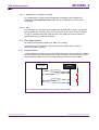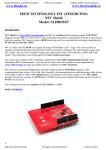
1
AN10609_3
PN532 C106 application note
Rev. 1.2 — January 5, 2010
Application note
Document information
Info
Content
Keywords
PN532C106, PN532 v1.6, Low Battery mode
Abstract
This document described
-
functionalities of PN532
-
changes between PN532C104 and PN532C106
AN10609_3
NXP Semiconductors
PN532 C106 application note
Revision history
Rev
Date
Description
1.0
March 10, 2008
First draft of AN10609_2, PN532 application note, C106 appendix.
It is based on AN10609_1 rev 1.1
1.1
September 7, 2009
update on application diagrams: RX path
1.2
January 5, 2010
Merge PN532 C104 and PN532 C106 application note
Add PN532 C106 SPI workaround, add SPI waveforms
Add how to use PN532 to read new Mifare cards.
Contact information
For additional information, please visit: http://www.nxp.com
For sales office addresses, please send an email to: [email protected]
<DOC_ID>
Application note
© NXP B.V. 2006. All rights reserved.
Rev. 1.2 — 1/14/2010
2 of 75
AN10609_3
NXP Semiconductors
PN532 C106 application note
1. Introduction
The PN532 is a highly integrated transmission module for contactless communication at
13.56 MHz including microcontroller functionality based on a 80C51 core with 40 Kbytes
of ROM and 1 Kbyte of RAM.
The PN532 combines a modulation and demodulation concept completely integrated for
different kinds of contactless communication methods and protocols at 13.56 MHz
(particularly Near Field Communication NFC), with an easy-to-use firmware for the
different supported modes and the required host interfaces.
The PN532 includes a switch to power an external SAM connected to S2C interface. It is
controlled by the embedded firmware.
HOST
CONTROLLER
Interface with host controller : SPI or I2C or HSU.
Possibly one or two additional lines (H_REQ, IRQ).
PN532
antenna
RF communication
Fig 1. Simplified system view
Error! Unknown document property name.
Application note
© Koninklijke Philips Electronics N.V. 2006. All rights reserved.
Rev 1.2 — 1/14/2010
3 of 75
AN10609_3
NXP Semiconductors
PN532 C106 application note
This document intends to allow the customer getting quickly started with the PN532. It
summarizes commands needed to use the PN532 as a reader, as a card, or in a NFC
peer-to-peer communication. It gives an overview on possible interfaces with the host
controller.
Detailed description of the PN532 firmware can be found in the PN532 User manual (cf.
References table below).
Full description of the PN532 IC can be found in the PN532 Datasheet.
This document underlines differences between PN532C104 (previous version not
produced anymore) and PN532C106.
The PN532C106 main differences compared with PN532C104:
-
Possible host interface: HSU, I2C or SPI mode 0 (no more SPI mode 1, 2, 3)
-
“Low battery” mode
“Low battery” mode is the start up mode of PN532C106. It is described page 21.
References
Ref.number
Document name
1
PN532 C106 user manual
UM0701-02
2
PN532 Product Datasheet
115430.pdf
3
NFC Transmission Module Antenna and RF
Design Guide
100720.pdf
4
Desfire cards specification
M075031.pdf
5
Mifare cards specification
http://www.nxp.com/products/identification/datasheets/
6
ISO/IEC 14443 specification (T=CL)
ISO/IEC 14443-3 specification
ISO/IEC 14443-4 specification
7
NFCIP-1 specification
ISO/IEC 18092 or ECMA340 specification
Glossary
NFC
Near Field Communication
HSU
High Speed UART
SMX
Philips SmartMX (Memory Extension)
PCR
Power, Clock and Reset controller
SAM
Secure Access Module
MINT
Multiple Interfaces
PMU
Power Management Unit
DEP
Data Exchange Protocol (see reference 7)
Error! Unknown document property name.
Application note
© Koninklijke Philips Electronics N.V. 2006. All rights reserved.
Rev 1.2 — 1/14/2010
4 of 75
AN10609_3
NXP Semiconductors
PN532 C106 application note
Pin correspondence: In the documents the following correspondence can be used in
the names of the pins:
PN532 Datasheet name
Application Note name
(C104 or C106)
(C104 or C106)
P70_IRQ
IRQ
P32_INT0
H_REQ
P50_SCL
SCL
HSU_RX
T_RX
HSU_TX
T_TX
IC correspondence: In the documents the following correspondence can be used in the
names of the IC:
Commercial Name
Application Note name
PN5321A3HN/C106
PN532C106
P5CN072
SMX
Error! Unknown document property name.
Application note
© Koninklijke Philips Electronics N.V. 2006. All rights reserved.
Rev 1.2 — 1/14/2010
5 of 75
AN10609_3
NXP Semiconductors
PN532 C106 application note
2. Interfaces with the host controller
2.1 PN532 block diagram
The PN532 is based on an 8051 core, with 40 Kbytes of ROM and 1Kbyte of RAM. The
chip contains a contactless UART, a contactless front end, a “PCR” block that controls
clocks and power.
It can be connected to the host controller in I2C, SPI or HSU (High Speed UART). One or
two more lines (IRQ and H_REQ) can be added. The interface is selectable using I0 and
I1 pins.
A SAM companion chip can be attached using S2C interface.
A part of the IC can be powered directly from a mobile battery (VBAT between 2.7V and
5.4V). The Pad power supply (PVDD) must be between 1.6V and 3.6V.
The SAM power supply SVDD is provided by the PN532.
P30
P31
P32 P33
IRQ
RS232
SCK or P72
MINT
ROM
40 kbyte
8051
FIFO
Power
switch, regulator,
LDO, power on reset
SVDD (output)
power for SAM interface
VDD (1.6 V to 3.6V)
VBAT (2.7 to 5.4V)
RAM
1 kbyte
ContactLess
UART
SPI
NSS or SCL
or D+ or Rx
RSTPD
I1
I2C
HSU
MISO or P71
MOSI or SDA
or D- or Tx
I0
FIFO, Mifare
Classic Unit, Frame
generation and
check
PCR
(Power Clock and
Reset controller)
ContactLess
Front End
RF Detector,
Demod, Antenna
driver
SIGIN
SIGOUT
P34
RX
LOADMOD
OSC 27.12MHz
Xtal
TX1
TX2
Fig 2. PN532 block diagram
Error! Unknown document property name.
Application note
© Koninklijke Philips Electronics N.V. 2006. All rights reserved.
Rev 1.2 — 1/14/2010
6 of 75
AN10609_3
NXP Semiconductors
PN532 C106 application note
2.2 Hardware changes compared to PN532C104
2.2.1 Hardware configuration pins
At start up, the normal mode must be selected by connecting P35 and IRQ as defined
below. The two other modes (RF field on and Emu Joiner) are special modes useful only
for tests purposes.
No external resistors are required on P35 and IRQ pins.
Interface Selection Pin
Normal mode
Normal mode
EmuJoiner
RF field On
P35
(pin #19)
IRQ
(pin #25)
1
1
DVDD/VBAT
PVDD
1
0
DVDD/VBAT
GND
0
1
GND
PVDD
0
0
GND
GND
Three interfaces are available: I2C, SPI and HSU (high speed UART). The interface is
selectable by hardware (pin I0 and I1).
Interface Selection Pin
HSU
I2C
SPI
I0
(pin #16)
I1
(pin #17)
0
0
GND
GND
1
0
DVDD
GND
0
1
GND
DVDD
The embedded software manages the communication with the host controller (I2C, SPI,
or HSU interface, protocol on the host link) and the communication on the RF side.
Error! Unknown document property name.
Application note
© Koninklijke Philips Electronics N.V. 2006. All rights reserved.
Rev 1.2 — 1/14/2010
7 of 75
AN10609_3
NXP Semiconductors
PN532 C106 application note
2.2.1.1
Additional lines (IRQ and H_REQ)
P31 is not used to choose between handshake or standard mode: PN532C106
implements only handshake mode, whatever P31 configuration (It can be let not
connected).
2.2.1.2 SPI
Only SPI mode 0 is implemented in PN532C106. Consequently, P30 (pin 24) and P33
(pin 33) states don’t configure anymore the SPI mode. They can be let not connected
To stay in LowVbat mode, NSS must be kept in high state even when PVDD is not
present (NSS low is a wake up condition).
2.3 Host link protocol
No changes compared to PN532C104. Refer to [1] and [8]
The protocol used on host link is fully described in the PN532 User manual (cf.
References table on page 4)
2.3.1 Standard frame
A basic exchange consists in a command frame sent by the host controller to the PN532,
an ACK frame sent by the PN532 as soon as the command is correctly received, and a
response frame, read by the host controller (polling mechanism or use of IRQ).
Controller
PN532
I
R
Q
Command Packet
ACK
Response Packet
ACK
01
Fig 3. Normal exchange between host controller and the PN532
Error! Unknown document property name.
Application note
© Koninklijke Philips Electronics N.V. 2006. All rights reserved.
Rev 1.2 — 1/14/2010
8 of 75
AN10609_3
NXP Semiconductors
PN532 C106 application note
Command and response frame structure is shown in figure 3.
00
00
FF
LEN LCS
TFI
PD0 PD1
……...
PDn DCS
00
Postamble
Packet Data Checksum
Packet Data
Specific PN532 Frame Identifier
Packet Length Checksum
Packet Length
Start of Packet Code
Preamble
Fig 4. Information frame
¾
PREAMBLE
¾
START CODE 2 bytes (00h and FFh)
¾
LEN
1 byte indicating the number of bytes in the data field
(TFI and PD0 to PDn)
¾
LCS
1 Packet Length Checksum LCS byte that satisfies the relation:
Lower byte of [LEN + LCS] = 00h
¾
TFI
1 byte the PN532 Frame Identifier, the value of this byte depends
on the way of the message
1 byte
- D4h in case of a frame from the system controller to the the PN532
- D5h in case of a frame from the the PN532 to the system controller
¾
DATA
¾
DCS
¾
POSTAMBLE
LEN-1 bytes of Packet Data Information
The first byte PD0 is the Command Code
1 Data Checksum DCS byte that satisfies the relation:
Lower byte of [TFI + PD0 + PD1 + … + PDn + DCS] = 00h
1 byte
ACK frame is described in figure 4.
00
00
FF
00
FF
00
Postamble
ACK Packet Code
Start of Packet Code
Preamble
Fig 5. ACK frame
List of available commands (PD0 byte) is provided in paragraph 3.2 on page 26.
Error! Unknown document property name.
Application note
© Koninklijke Philips Electronics N.V. 2006. All rights reserved.
Rev 1.2 — 1/14/2010
9 of 75
AN10609_3
NXP Semiconductors
PN532 C106 application note
2.3.2 Extended frame
The information frame has an extended definition allowing exchanging more data
between the host controller and the the PN532 (theoretically up to 64kB).
In the firmware implementation of the the PN532, the maximum length of the packet data
is limited to 264 bytes (265 bytes with TFI included).
The structure of this frame is the following:
00
00
FF
FF
FF
LENM
LENL
LCS
TFI
PD0 PD1
……...
PDn DCS
00
Postamble
Packet Data Checksum
Packet Data
Specific TFI
Packet Length Checksum
Packet Length
Start of Packet Code
Preamble
Normal Packet Length Checksum
: Fixed to FF value
Normal Packet Length
: Fixed to FF value
Fig 6. Extended Information frame
The normal LEN and LCS fields are fixed to the 0xFF value, which is normally
considered as an erroneous frame, due to the fact that the checksum does not fit.
The real length is then coded in the two following bytes LENM (MSByte) and LENL
(LSByte) with:
LENGTH = LENM x 256 + LENL coding the number of bytes in the data field (TFI and
PD0 to PDn)
¾
LCS
1 Packet Length Checksum LCS byte that satisfies the relation:
Lower byte of [LENM + LENL + LCS] = 0x00,
¾
DATA
LENGTH-1 bytes of Packet Data Information
The first byte PD0 is the Command Code.
The host controller, for sending frame whose length is less than 255 bytes, can also use
this type of frame.
But, the the PN532 always uses the suitable type of frame, depending on the length
(Normal Information Frame for frame <= 255 bytes and Extended Information Frame for
frame > 255 bytes).
Error! Unknown document property name.
Application note
© Koninklijke Philips Electronics N.V. 2006. All rights reserved.
Rev 1.2 — 1/14/2010
10 of 75
AN10609_3
NXP Semiconductors
PN532 C106 application note
2.4 Typical application diagrams
Error! Unknown document property name.
Application note
© Koninklijke Philips Electronics N.V. 2006. All rights reserved.
Rev 1.2 — 1/14/2010
11 of 75
AN10609_3
NXP Semiconductors
PN532 C106 application note
2.4.1 I2C application diagram
To host controller. Low state = reset. High
state = functional mode. RSTPD_N must not
exceed min(VBAT, 3.6V) (e.g. use a resistor
bridge on VBAT)
DVDD
To SMX
100 nF
To SMX To SMX To SMX
10 µF
100 nF
47 k
VBAT
100 nF
HREQ
4.7 µF
40 39
38
36
35
34
33
32
P31
P32
P33
P34
SIGOUT
SIGIN
SVDD
37
NC
1
31
30
2
29
3
28
4
27
5
26
LOADMOD
560nH
TGND1
To antenna
TX1
TVDD
To antenna
PN532
6
25
TX2
DVDD
560nH
7
24
8
23
9
22
TGND2
AVDD
100 nF
VMID
10
MISO
NC
MOSI
3.3 k
2.7 k
1 nF
Test point
Test point
DVDD
NSS
RSTOUTN
SCL
IRQ
PVDD
P30
NC
PVDD
NC3
100 nF
22 pF
Fig 7. I2C PN532C106 application diagram
Error! Unknown document property name.
Application note
© Koninklijke Philips Electronics N.V. 2006. All rights reserved.
Rev 1.2 — 1/14/2010
To Host controller
NC
27.12 MHz
22 pF
3.3k
To Host controller
NC2
20
P35
18 19
PVDD
SDA
NC (internally
connected to
DVDD)
17
TESTEN
15 16
I1
14
I0
13
XTAL2
12
XTAL1
To antenna
NC
21
11
AUX2
RX
AGND
1k
AUX1
100 nF
PVDD
SCK
NC1
DGND
RSTPDN
VBAT
100 nF
To Host controller
NC
DVDD
DVDD
12 of 75
To Host controller
start up high (PVDD) or low
AN10609_3
NXP Semiconductors
PN532 C106 application note
2.4.2 SPI communication
2.4.2.1
SPI and LowVbat mode
Using Low Vbat functionality and SPI interface requires the following work around.
1. In case LowVbat functionality is not required
Always keep PVDD (and Vbat) present. Proceed as described in paragraph 2.5.2
2. In case LowVbat functionality is required
The interface pins will be used to achieve LowVbat mode. Therefore they must be connected to the host
controller.
Before switching off the host controller, change I0 to 1 and I1 to 0 (this put the PN532 in I2C
configuration)
Host sends a reset pulse (minimum 20ns, see datasheet p209) to PN532 via RSTPD_N
Wait a time off (2ms, see datasheet p209)
The PN532 will go in LowVbat mode and stays in this mode (25µA)
Î An external reader can communicate with the SMX as a card
To wake up the PN532 (to exit LowVbat mode) and recover SPI communication
Host controller change I0 to 0 and I1 to 1 (restore SPI configuration)
Host controller sends a reset pulse (minimum 20ns) to PN532 via RSTPD_N
Wait a time off (2 ms)
Host controller sets NSS wake-up (high to low, CSN)
Î SPI communication can be performed (e.g. send command SAMConfiguration ’14 01’ to
switch to standard mode).
When changing I0 and I1, the internal configuration of pins 27, 28, 29, 30 (interface lines) is changed. See
table in paragraph 2.4.4 Default pin configuration.
Warning: It is also possible to switch to I0 and I1 to 0 (HSU). The advantage is that only I1 need to be
toggle. But in this mode, pin 28 MOSI/TX is strongly push pulled to high by PN532, which can prevent the
communication between the host controller and other chips on the SPI bus.
2.4.2.2 SPI application diagram
Error! Unknown document property name.
Application note
© Koninklijke Philips Electronics N.V. 2006. All rights reserved.
Rev 1.2 — 1/14/2010
13 of 75
AN10609_3
NXP Semiconductors
PN532 C106 application note
To host controller. Low state = reset. High
state = functional mode. RSTPD_N must not
exceed min(VBAT, 3.6V) (e.g. use resistor
bridge on VBAT)
DVDD
To SMX
100 nF
To SMX To SMX To SMX
10 µF
100 nF
47 k
VBAT
100 nF
4.7 µF
40 39
DGND
560nH
38
36
35
34
33
32
P31
P32
P33
P34
SIGOUT
SIGIN
SVDD
37
NC
1
31
30
2
29
3
28
4
27
5
26
LOADMOD
TGND1
To antenna
TX1
TVDD
To antenna
PN532
6
25
TX2
DVDD
560nH
7
24
8
23
TGND2
AVDD
100 nF
9
22
10
21
VMID
To Host controller
MOSI
To Host controller
NSS
RSTOUTN
NC
IRQ
PVDD
P30
To Host controller
start up high (PVDD) or low
NC
PVDD
NC3
100 nF
NC2
20
P35
To Host controller
MISO
NC (internally
connected to
DVDD)
2.7 k
18 19
TESTEN
17
I1
15 16
I0
14
XTAL2
13
AUX2
To antenna
12
XTAL1
11
AGND
1k
RX
AUX1
100 nF
To Host controller
SCK
NC1
100 nF
RSTPDN
VBAT
NC
DVDD
DVDD
1 nF
Test point
Test point
27.12 MHz
22 pF
22 pF
To Host controller
To Host controller
Fig 8. SPI PN532C106 application diagram
Error! Unknown document property name.
Application note
© Koninklijke Philips Electronics N.V. 2006. All rights reserved.
Rev 1.2 — 1/14/2010
14 of 75
AN10609_3
NXP Semiconductors
PN532 C106 application note
2.4.2.3
SPI communication details
The PN532 is slave. A Status byte (Bit 0 of Status byte) indicates if the PN532 is ready to give a response
or not. First byte sent on MOSI by the host controller indicates which operation will be performed:
xxxx xx10 : Read (by the host) Status byte
xxxx xx01 : Write data (transmission from the host to the PN532)
xxxx xx11 : Read data (transmission from the PN532 to the host)
After having sent a command, the host controller must wait for bit 0 of Status byte equals 1 before reading
the data from the PN532.
Bytes are transmitted LSB first.
NSS must be toggle as shown in the user manual (reference 1) or in the next figures.
2.4.2.4 SPI waveforms
SPI waveforms for GetFirmware version command (example with SPI freq. 500 kHz).
Error! Unknown document property name.
Application note
© Koninklijke Philips Electronics N.V. 2006. All rights reserved.
Rev 1.2 — 1/14/2010
15 of 75
AN10609_3
NXP Semiconductors
PN532 C106 application note
Fig 9. Write the command.
Error! Unknown document property name.
Application note
© Koninklijke Philips Electronics N.V. 2006. All rights reserved.
Rev 1.2 — 1/14/2010
16 of 75
AN10609_3
NXP Semiconductors
PN532 C106 application note
Fig 10. Read the Status.
Error! Unknown document property name.
Application note
© Koninklijke Philips Electronics N.V. 2006. All rights reserved.
Rev 1.2 — 1/14/2010
17 of 75
AN10609_3
NXP Semiconductors
PN532 C106 application note
Fig 11. Read the ACK frame.
Fig 12. Read the Status.
Error! Unknown document property name.
Application note
© Koninklijke Philips Electronics N.V. 2006. All rights reserved.
Rev 1.2 — 1/14/2010
18 of 75
AN10609_3
NXP Semiconductors
PN532 C106 application note
Fig 13. Read the Response frame.
Error! Unknown document property name.
Application note
© Koninklijke Philips Electronics N.V. 2006. All rights reserved.
Rev 1.2 — 1/14/2010
19 of 75
AN10609_3
NXP Semiconductors
PN532 C106 application note
2.4.3 HSU application diagram
To host controller. Low state = reset. High
state = functional mode. RSTPD_N must not
exceed min(VBAT, 3.6V) (e.g. use a resistor
bridge on VBAT)
DVDD
To SMX
100 nF
To SMX To SMX To SMX
10 µF
100 nF
47 k
VBAT
100 nF
HREQ
4.7 µF
40 39
560nH
38
36
35
34
33
32
P31
P32
P33
P34
SIGOUT
SIGIN
SVDD
37
NC
1
31
30
2
29
LOADMOD
TGND1
To antenna
TX1
TVDD
To antenna
28
3
27
4
26
5
PN532
6
25
TX2
DVDD
560nH
7
24
8
23
TGND2
AVDD
100 nF
9
22
10
21
VMID
NC
NC
MOSI
To Host controller
NSS
RSTOUTN
Rx
NC
IRQ
PVDD
P30
NC
PVDD
NC3
100 nF
NC2
20
1 nF
Test point
Test point
27.12 MHz
22 pF
22 pF
Fig 14. HSU PN532C106 application diagram
Error! Unknown document property name.
Application note
© Koninklijke Philips Electronics N.V. 2006. All rights reserved.
Rev 1.2 — 1/14/2010
To Host controller
Tx
NC (internally
connected to
DVDD)
2.7 k
18 19
P35
17
TESTEN
15 16
I1
14
I0
13
XTAL2
To antenna
12
AUX2
11
XTAL1
RX
AGND
1k
AUX1
100 nF
SCK
MISO
NC1
DGND
RSTPDN
VBAT
100 nF
To Host controller
NC
DVDD
DVDD
20 of 75
To Host controller
start up high (PVDD) or low
AN10609_3
NXP Semiconductors
PN532 C106 application note
2.4.4 Default pin configuration
Consequently, the default pin configuration is as described in the PN532 datasheet. (The
default pin configuration is not changed by the PN532C106 firmware).
Pin
I0
Configuration
Additional information
Input
Connect directly to DVDD or to GND (no need of
external resistor)
PVDD
Power pin
Externally supplied regulated voltage, 1.6V to 3.6V
RSTPD_N
Input
NFC reset signal. (Low state = reset)
I1
RSTPD_N must never exceed min(3.6 V, VBAT)
P30 / UART_RX
Quasi bi directional
No need of external resistor.
When connected to the P5CN072, to be used in Virtual
Card mode, P34 / SIC_CLK shall be connected to
P5CN072 I02
P31 / UART_TX
P32_INT0
P33_INT1
P34 / SIC_CLK
P35
P70_IRQ
Quasi bi directional
No need of external resistor.
In the Application Note P70_IRQ will be written as IRQ
when used as interrupt line.
MISO / P71
In I2C mode: Quasi bi directional
No need of external resistor.
In SPI: Push pull
No need of external resistor
In HSU: Quasi bi directional
No need of external resistor
In I2C mode: Quasi bi directional
No need of external resistor.
In SPI: Input
No need of external resistor.
In HSU: Quasi bi directional
No need of external resistor
In I2C mode: Open drain
Use pull up, 1k/V. E.g. for PVDD = 3.3V, 3.3 k pull-up.
In SPI: Input
No need of external resistor
In HSU: Push pull
No need of external resistor
In I2C mode: Open drain
Use pull up, 1k/V. E.g. for PVDD = 3.3V, 3.3 k pull-up.
In SPI: Input
Use resistor bridge or LDO and pull up to be able
• to keep NSS high even when PVDD =
0 (to stay in LowVBAT mode)
• to force a low state to wake up.
In HSU: Input
No need of external resistor
SCK / P72
MOSI / SDA /
HSU_TX
NSS / P50_SCL /
HSU_RX
<DOC_ID>
Application note
© NXP B.V. 2006. All rights reserved.
Rev. 1.2 — 1/14/2010
21 of 75
AN10609_3
NXP Semiconductors
PN532 C106 application note
2.5 How to start the PN532C106?
2.5.1 LowVbat mode (PN532C106 start up default mode)
PN532C106 starts in “Low Vbat” mode.
In this mode, the PN532C106 is in virtual card mode when an external field is
present, and in power down mode otherwise. In this mode, an external reader can
communicate with the SMX (connected to PN532C106 via its S2C interface).
¾ No interrupt (IRQ) will be returned by PN532C106 to its host controller.
¾ The host controller cannot wake up PN532 using HREQ/P32 line (pin 32).
This mode is functional even if PVDD = 0V. (VBAT between 2.7V and 5.5V)
LowVBAT diagram and power consumption:
Power-up the VBAT
of the PN532 C106
(PVDD = baseband supply
has no influence)
The PN532 is configured in the so-called
LowVbat mode
The functional mode of the PN532 is
Soft Power Down mode.
Its current consumption is around 20uA.
PN532 C106 goes out of external field
PN532 C106 goes into external RF field
The PN532 is configured in the so-called
LowVbat mode
The functional mode of the PN532 in the field is
Card Emualtion mode.
Its current consumption is around 20mA .
<DOC_ID>
Application note
© NXP B.V. 2006. All rights reserved.
Rev. 1.2 — 1/14/2010
22 of 75
AN10609_3
NXP Semiconductors
PN532 C106 application note
2.5.2 To go out Low Vbat mode (i.e. to wake up PN532C106 after start up)
To go out “Low Vbat” mode, there are three conditions
• PVDD must be present.
• Moreover, to wake up the PN532C106, the host controller must
• In I2C
Send PN532 I2C address (48h). The PN532 will stretch low the SCL line during
1 ms (can be less depending on the quartz). The host controller shall wait for the
end of the stretching.
• In SPI
Set NSS low during 1 ms (can be less depending on the quartz)
• In HSU
Send a preamble 55 55 00 00 00 00 00 FF then Len LCS ….
• The host controller must send one of the following commands (using the wake up
conditions described just above)
− Either it wants to stay in virtual card mode. Then it shall send a command to
enable the interrupt generation (IRQ) by PN532C106. (The IRQ warns the host
controller that a transaction occurred between an external reader and the SMX).
The command to send is “SAM Configuration” with parameter Mode = virtual (02h)
and parameter IRQ use = yes (either put value 01h or omit the parameter).
So the command is ‘14 02 00’ (or ‘14 02 00 01’)
− Or it wants to go to normal mode. Then it shall send “SAM Configuration” with
parameter Mode = normal (01h). So the command is ‘14 01’
Once woken up, any command can be send like in PN532C104 (with handshake
mode)
NB: As soon as PVDD is present, the host controller must send a command to
enable the interrupt generation (IRQ) by PN532C106. (The IRQ warns the host
controller that a transaction occurred between an external reader and the
SMX). The command to send is “SAM Configuration” with parameter Mode = virtual
(02h) and parameter IRQ use = yes (either put value 01h or omit the parameter)
14 02 00 (or 14 02 00 01)
<DOC_ID>
Application note
© NXP B.V. 2006. All rights reserved.
Rev. 1.2 — 1/14/2010
23 of 75
AN10609_3
NXP Semiconductors
PN532 C106 application note
Instructions described in this paragraph are represented on the following diagram:
Power-Off
VBAT present (>2.5V)
PVDD has no impact
LowVbat mode
= Card Emulation with
No HREQ functionality
Send 14 01
(with no HREQ during command)
Send 14 02 00
(with no HREQ during command)
Normal mode
with HREQ and IRQ informations
See Remark.
Card Emulation mode
with HREQ and IRQ informations
See Remark.
Battery Voltage too low for Mobile Call
Send 14 02 00 00
(with HREQ and IRQ informations)
Remark: In that modes, in order to fullfill the application requirements, any commands of the User
Manual can be sent using HREQ and IRQ informations. These scenarios are not described in the
diagram.
<DOC_ID>
Application note
© NXP B.V. 2006. All rights reserved.
Rev. 1.2 — 1/14/2010
24 of 75
AN10609_3
NXP Semiconductors
PN532 C106 application note
3. The PN532 commands
3.1 Global view
The PN532 can be access using directly the firmware API described in reference 1 and
in the following pages (interface B in the figure 17). Or an upper software layer can be
used (NXP can provide this layer called Hardware Abstraction Layer (HAL) – HAL is the
interface A in the figure 17).
Note: PN51x, PNxxx, RCxxx represents other NXP NFC products. PN53x represents
PN531 or the PN532 product.
Fig 15. Possible software/hardware interface
The next paragraph described the “interface B”, i.e. the firmware commands.
<DOC_ID>
Application note
© NXP B.V. 2006. All rights reserved.
Rev. 1.2 — 1/14/2010
25 of 75
AN10609_3
NXP Semiconductors
PN532 C106 application note
3.2 The PN532 embedded software API: commands and errors lists
3.2.1 Commands codes
The PN532 The PN532
as Initiator
as Target
Command
Command
Code
M i s c e l l a n e o u s
Diagnose
X
X
0x00
GetFirmwareVersion
X
X
0x02
GetGeneralStatus
X
X
0x04
ReadRegister
X
X
0x06
WriteRegister
X
X
0x08
ReadGPIO
X
X
0x0C
WriteGPIO
X
X
0x0E
SetSerialBaudRate
X
X
0x10
SetParameters
X
X
0x12
SAMConfiguration
X
X
0x14
PowerDown
X
X
0x16
RFConfiguration
X
X
0x32
RFRegulationTest
X
X
0x58
R F
c o m m u n i c a t i o n
I n i t i a t o r
InJumpForDEP
X
0x56
InJumpForPSL
X
0x46
InListPassiveTarget
X
0x4A
InATR
X
0x50
InPSL
X
0x4E
InDataExchange
X
0x40
InCommunicateThru
X
0x42
InDeselect
X
0x44
InRelease
X
0x52
InSelect
X
0x54
<DOC_ID>
Application note
© NXP B.V. 2006. All rights reserved.
Rev. 1.2 — 1/14/2010
26 of 75
AN10609_3
NXP Semiconductors
PN532 C106 application note
The PN532 The PN532
as Initiator
as Target
Command
0x60
X
InAutoPoll
Command
Code
T a r g e t
TgInitAsTarget
X
0x8C
TgSetGeneralBytes
X
0x92
TgGetData
X
0x86
TgSetData
X
0x8E
TgSetMetaData
X
0x94
TgGetInitiatorCommand
X
0x88
TgResponseToInitiator
X
0x90
TgGetTargetStatus
X
0x8A
3.2.2 Errors codes
Error cause
Error code
Time Out, the target has not answered
0x01
A CRC error has been detected by the contactless UART
0x02
A Parity error has been detected by the contactless UART
0x03
During a MIFARE anticollision/select operation, an erroneous
Bit Count has been detected
0x04
Framing error during MIFARE operation
0x05
An abnormal bit-collision has been detected during bit wise
anticollision at 106 kbps
0x06
Communication buffer size insufficient
0x07
RF Buffer overflow has been detected by the contactless
UART (bit BufferOvfl of the register CL_ERROR)
0x09
In active communication mode, the RF field has not been
switched on in time by the counterpart (as defined in NFCIP-1
standard)
0x0A
RF Protocol error (cf. reference [4], description of the
CL_ERROR register)
0x0B
<DOC_ID>
Application note
© NXP B.V. 2006. All rights reserved.
Rev. 1.2 — 1/14/2010
27 of 75
AN10609_3
NXP Semiconductors
PN532 C106 application note
Error cause
Error code
Temperature error: the internal temperature sensor has
detected overheating, and therefore has automatically
switched off the antenna drivers
0x0D
Internal buffer overflow
0x0E
Invalid parameter (range, format, …)
0x10
DEP Protocol: The the PN532 configured in target mode does
not support the command received from the initiator (the
command received is not one of the following: ATR_REQ,
WUP_REQ, PSL_REQ, DEP_REQ, DSL_REQ, RLS_REQ,
ref. [1]).
0x12
DEP Protocol / Mifare / ISO/IEC 14443-4: The data format
does not match to the specification.
Depending on the RF protocol used, it can be:
0x13
•
Bad length of RF received frame,
•
Incorrect value of PCB or PFB,
•
Invalid or unexpected RF received frame,
•
NAD or DID incoherence.
Mifare: Authentication error
0x14
ISO/IEC 14443-3: UID Check byte is wrong
0x23
DEP Protocol: Invalid device state, the system is in a state
which does not allow the operation
0x25
Operation not allowed in this configuration (host controller
interface)
0x26
This command is not acceptable due to the current context of
the the PN532 (Initiator vs. Target, unknown target number,
Target not in the good state, …)
0x27
The the PN532 configured as target has been released by its
initiator
0x29
The PN5321 and ISO/IEC 14443-3B only: the ID of the card
does not match, meaning that the expected card has been
exchanged with another one.
0x2A
The PN5321 and ISO/IEC 14443-3B only: the card previously
activated has disappeared.
0x2B
Mismatch between the NFCID3 initiator and the NFCID3
target in DEP 212/424 kbps passive.
0x2C
An over-current event has been detected
0x2D
NAD missing in DEP frame
0x2E
<DOC_ID>
Application note
© NXP B.V. 2006. All rights reserved.
Rev. 1.2 — 1/14/2010
28 of 75
AN10609_3
NXP Semiconductors
PN532 C106 application note
3.3 The PN532 various modes
This paragraph summarizes the PN532 functionalities and shows which commands are
associated to them.
The PN532 firmware implements functions to easily behave:
-
As a NFC initiator or a NFC target (according to NFCIP-1 specification).
In this mode, RF communication is according to NFCIP-1 specification. Two NFC
devices can communicate together (peer to peer communication). One device is the
initiator: it starts the exchange and chooses the mode. The other device is the target.
Passive mode or active mode can be used. In active mode, each device generates
RF field when it transmits data (and switches RF field off at the end of the
transmission). In passive mode, only the initiator generates RF field. The target
answers in a load modulation scheme.
HOST
CONTROLLER
e.g. Mobile phone
PN532
PN532
HOST
CONTROLLER
e.g. PDA
RF communication
Fig 16. Peer to peer communication (NFC initiator and NFC target)
-
As a Mifare reader (Mifare protocol).
In this mode, RF communication is according to Mifare specification. the PN532
behaves as a Mifare reader. It can communicate with Mifare cards.
HOST
CONTROLLER
e.g. Mobile phone
PN532
RF communication
Fig 17. The PN532 as a Mifare reader
The PN532 has been tested with Mifare 1k, 4k, Ultralight, and DesFire cards.
<DOC_ID>
Application note
© NXP B.V. 2006. All rights reserved.
Rev. 1.2 — 1/14/2010
29 of 75
AN10609_3
NXP Semiconductors
PN532 C106 application note
-
As a T=CL reader (ISO/IEC 14443-4 protocol)
In this mode, RF communication is according to ISO/IEC 14443-4 specification. the
PN532 behaves as an ISO/IEC 14443-4 reader. It can communicate with ISO/IEC
14443-4 cards (only ISO compliant cards are supported).
(The PN532 has been tested with CD97BX, CD light, Desfire, P5CN072 (SMX) as
ISO/IEC 14443-4 (with JCOP OS))
-
As a Jewel card reader
The PN532 can communicate with Innovision Jewel cards. It has been tested with
IRT5001 card.
-
As a FeliCa reader (FeliCa protocol)
In this mode, RF communication is according to FeliCa specification. the PN532 has
been tested with FeliCa RCS_860 and RCS_854
-
As a ISO/IEC 1443-A card
The PN532 is able to answer to an ISO/IEC 1443-4A reader. It contains a predefined
ATS (only historical bytes are configurable). In this mode, ATS will be sent
automatically to the reader which has sent a RATS. the PN532 handles automatically
waiting time extension (S(WTX)). The command from the reader is transmitted to the
host controller. The host controller builds the response and transmits it to the PN532.
the PN532 handles the encapsulation in ISO/IEC 1443-4 frame. Maximum up to 256
data bytes can be transmitted between the reader and the the PN532 (“short
APDU”).
<DOC_ID>
Application note
© NXP B.V. 2006. All rights reserved.
Rev. 1.2 — 1/14/2010
30 of 75
AN10609_3
NXP Semiconductors
PN532 C106 application note
-
As a virtual card (in combination with a secure smart card)
In this mode, the PN532 is combined with a secure smart card. An external reader
sees the set the PN532+secure smart card as a contactless card.
HOST
CONTROLLER
PN532
S2C interface
SMX
Connection with secure
smart card
RF communication
Mifare Reader
Fig 18. Virtual card mode
RFConfiguration command
This command, described in reference 1, allows changing some registers settings than
can influence the RF communication. The default values are described in reference 1.
The tuning depends on the environment, on the antenna and on the communication
mode.
Very few commands are needed to set up RF communication between the PN532 and
another device (reader, card, or other NFC device). The PN532 executes different RF
processes, depending on the type of communication, but from the host controller to
the PN532, same commands are used (whatever the baudrate, the mode etc):
Paragraphs below explain which functions to use to communicate in each mode.
<DOC_ID>
Application note
© NXP B.V. 2006. All rights reserved.
Rev. 1.2 — 1/14/2010
31 of 75
AN10609_3
NXP Semiconductors
PN532 C106 application note
3.3.1 How to use the PN532 as a Mifare reader?
3.3.1.1
Command supported by PN532 firmware
The Mifare commands supported by the PN532 firmware are listed in reference 1 and in
the following paragraphs.
For other commands, see 3.3.1.2
Typical sequence (example):
-
Scanning for targets (cards) in the field,
-
Possibly authenticate with the card,
-
Read out the card memory (or any other Mifare commands, such as write),
-
Halt the card, select another one, and perform any Mifare command with it
This typical sequence can be performed with the following commands:
-
InListPassivTarget, to initialise one (several) cards (maximum two cards at the
same time)
-
InDataExchange, to send Mifare commands
-
InSelect, InDeselect, and InRelease to select, and release the card (this is
optional, see paragraph 3.3.7.3 on page 56).
Warning:
In case the card initialized indicates it supports ISO/IEC 14443-4 protocol (bit 5 of SAK,
cf. ISO/IEC 14443-3 specification), InListPassiveTarget command of the PN532 performs
automatically ISO/IEC 14443-4 activation (i.e. RATS sending). To disable automatic
RATS sending, SetParameter command must be used (cf. REFERENCE 1).
Table 1.
SetParameter command usage to enable or disable automatic RATS sending (ISO/IEC 14443-4 mode)
Action
Disable automatic
sending of RATS
command
1
Command
12
24
Command explanation
Command code: SetParameters
Response
13
Response explanation
Response command code
Automatic ATR_RES = 1
Automatic ISO/IEC 1443-4A card emu =
1
RATS will not be performed automatically by next InListPassiveTarget.command, even if the card indicates it supports ISO 14443-4
Enable automatic
12
sending of RATS
34
command
(default
configuration of the
PN532 at power
up)
Command code: SetParameters
13
Automatic RATS = 1
Automatic ISO/IEC 1443-4A card emu =
1
<DOC_ID>
Application note
Response command code
Automatic ATR_RES = 1
© NXP B.V. 2006. All rights reserved.
Rev. 1.2 — 1/14/2010
32 of 75
AN10609_3
NXP Semiconductors
PN532 C106 application note
RATS will be performed automatically by next InListPassiveTarget.command, if the card indicates it supports ISO 14443-4
Mifare commands are briefly described hereafter. Refer to Mifare card
documentation to have a more detailed description of the Mifare command set
The Mifare specific command byte Cmd may take one of the possible values:
60h / 61h
Authentication A / Authentication B (Mifare Standard)
Performs authentication sequence.
30h
16 bytes reading
Read one data block (16 bytes) at the selected address of the card.
A0h
16 bytes writing (Mifare Standard)
Write one data block (16 bytes) to the selected address of the card.
A2 h
4 bytes writing (Mifare Ultralight)
Write one data block (16 bytes) to the selected address of the card.
C1 h
Increment
Increment the value block at the selected address of the card. The data structure of
the value block must be written in advance with a standard write command.
Data structure
Byte
0
3
Value
4
7
Value
complement
8
11
Value
12
13
14
15
Addr
Addr
complement
Addr
Addr
complement
C0 h
Decrement
Decrement the value block at the selected address of the card. The data structure of
the value block must be written in advance with a standard write command.
B0h
Transfer:
This function writes the prior calculated at the selected address of the card. It must
be called directly after Increment, Decrement or Restore.
C2h
Restore
This function restores the value block at the selected address of the card.
<DOC_ID>
Application note
© NXP B.V. 2006. All rights reserved.
Rev. 1.2 — 1/14/2010
33 of 75
AN10609_3
NXP Semiconductors
PN532 C106 application note
Mifare Ultralight cards
They support only A2h and 30h commands.
Command code
30h
A2h
Command
Parameter
1 byte address
1 byte address
Command Data
field
4 bytes
Response
16 bytes
-
Mifare Standard cards
Authentication is required before any access to Mifare Standard memory.
Command code
Command
Command Data
Response
Parameter
field
60h
1 byte address
KeyA (6 bytes,
default value FFh)
followed by UID (4
bytes)
61h
1 byte address
KeyB (6 bytes,
default value FFh)
followed by UID (4
bytes)
30h
1 byte address
16 bytes
A0h
1 byte address
16 bytes
C1h
1 byte address
4 byte increment
value (lower byte
first)
C0h
1 byte address
4 byte decrement
value (lower byte
first)
B0h
1 byte address
C2h
1 byte address
Refer to Mifare card documentation to have a more detailed description of the
Mifare command set
The table on next page shows how to use some of those commands (how to fill the
parameters, which bytes are returned in response…).
<DOC_ID>
Application note
© NXP B.V. 2006. All rights reserved.
Rev. 1.2 — 1/14/2010
34 of 75
AN10609_3
NXP Semiconductors
PN532 C106 application note
Table 2.
The PN532 as a Mifare reader
Action
Scan for 2 targets
in the field and
initialize them
1
Command
4A
02
Command explanation
Command code: InListPassivTargets
Number of cards to initialize (if present
in the field)
00
Baud rate = 106 kbits/sec.
Response
4B
02
01
04 00
08
04
12 67 58 32
02
44 00
00
08
88 04 B6 E4 00 00
00 00
Response explanation
Response command code
2 targets detected
Target number 1
SENS_RES(2) of target 1
SEL_RES(2) of target 1
NFCID1 length = 4 bytes
NFCID1 of target 1
Target number 2
SENS_RES(2) of target 2
SEL_RES(2) of target 2
NFCID1 length = 8 bytes
NFCID1 of target 2
Target 1 is a Mifare Standard card and target 2 is a Mifare Ultralight card. The 2 cards are initialised. Card 1 is in halt state.
Authenticate with
Mifare Standard
card
40
01
60
07
FF FF FF
FF FF FF
12 67 58 32
Command code: InDataExchange
41
Response command code
The cmd is intended to target number 1
00
Status = 0 (OK, no error)
Mifare cmd code (authenticate)
Mifare address
Default authentication key (last bytes
are NFCID1 bytes)
Card2 has been put in halt state. Card1 has been wake up and authentication has been performed.
Read out card 1
memory
40
01
30
04
Command code: InDataExchange
The cmd is intended to target number 1
Mifare cmd code (read 16 bytes)
Mifare address
41
00
EE EE EE EE EE
EE EE EE
EE EE EE EE EE
EE EE EE
Response command code
Status = 0 (OK, no error)
Bytes read (example)
Card2 is still in halt state. Any Mifare commands, for example Read 16 bytes, can be sent to card 2 with InDataExchange function.
Halt card 1, select 40
card 2 and write in 02
card 2 memory
A2
08
FF FF FF
FF
Command code: InDataExchange
The cmd is intended to target number 2
Mifare cmd code (write 4 bytes)
Mifare address
Bytes to be written
41
00
Response command code
Status = 0 (OK, no error)
Card1 has been put in halt state. Card 2 has been wake up.
Any Mifare commands, for example Write 4 bytes, can be sent to card 2 with InDataExchange function.
Halt card 2
44
01
Command code: InDeselect
45
Response command code
The cmd is intended to target number 1
00
Status = 0 (OK, no error)
HALT REQ is sent with InDeselect command.
(1)
Command code and command parameters. Mandatory protocol encapsulation is not represented.
<DOC_ID>
Application note
© NXP B.V. 2006. All rights reserved.
Rev. 1.2 — 1/14/2010
35 of 75
AN10609_3
NXP Semiconductors
PN532 C106 application note
(2)
SENS_RES and SEL_RES coding is described in ISO/IEC 18092 specification.
Timeout and number of retries
Activation phase (InListPassiveTarget command)
By default, the PN532 is configured to retry to detect a card as long as there is no
card detected. It can be changed using RFConfiguration command, item 5
(MaxRtyPassiveActivation parameter, c.f. UM0502-05).
If there is no card in the field, a timeout occurs after 5 ms. Either the PN532 retries to
find a card, if MaxRtyPassiveActivation > 1, or it sends a response to its host
controller, indicating that zero target has been found.
Communication phase (InDataExchange command)
By default, the timeout is set to 51.2 ms. It can be changed using RFConfiguration
command item 2 (UM0501-02 page 80).
Deactivation phase (InDeselect/InRelease command)
InDeselect or InRelease commands perform a HALTA request. The return status is
always “No error” (00h), even if the card did not respond (within 5 ms).
Note: It is not needed to use InDeselect (and InSelect) command to handle two
cards. Indeed, when using InDataExchange command, the PN532 automatically
wakes up the card corresponding to the desired TgNb, and automatically put in
HALT state the other one.
3.3.1.2
Other Mifare commands
PN532 InDataExchange command supports Mifare commands listed in the user manual
(reference 1). Commands not mentioned will return an error. However, it is possible to
send other commands (e.g. Mifare Plus new commands), using InCommunicateThru
command.
// test InCommunicateThru for sending commands to Mifare Plus card
// disable autoRATS to stay in the Mifare mode
PC -> IFD : SET TAMA PARAMETERS
00 00 FF 03 FD D4 12 00 1A 00
IFD -> PC : ACK
00 00 FF 00 FF 00
IFD -> PC : SET TAMA PARAMETERS EXECUTED
00 00 FF 02 FE D5 13 18 00
// Look for a 106 kbps card
PC -> IFD : INITIATOR : LIST PASSIVE TARGETS
00 00 FF 04 FC D4 4A 01 00 E1 00
<DOC_ID>
Application note
© NXP B.V. 2006. All rights reserved.
Rev. 1.2 — 1/14/2010
36 of 75
AN10609_3
NXP Semiconductors
PN532 C106 application note
IFD -> PC : ACK
00 00 FF 00 FF 00
IFD -> PC : INITIATOR : LIST PASSIVE TARGETS EXECUTED
00 00 FF 0F F1 D5 4B 01 01 00 42 18 07 04 66 C5
04 05 06 07 38 00
// read TxMode and RxMode registers
PC -> IFD : READ REGISTERS
00 00 FF 06 FA D4 06 63 02 63 03 5B 00
IFD -> PC : ACK
00 00 FF 00 FF 00
IFD -> PC : READ REGISTERS EXECUTED
00 00 FF 04 FC D5 07 80 80 24 00
// Change CRC of RxMode : disable CRC Rx
PC -> IFD : WRITE REGISTERS
00 00 FF 05 FB D4 08 63 03 00 BE 00
IFD -> PC : ACK
00 00 FF 00 FF 00
IFD -> PC : WRITE REGISTERS EXECUTED
00 00 FF 02 FE D5 09 22 00
// send Mifare Plus command A8
PC -> IFD : INITIATOR : COMMUNICATE THRU
00 00 FF 15 EB D4 42 A8 02 90 11 11 11 11 11 11
11 11 11 11 11 11 11 11 11 11 A0 00
IFD -> PC : ACK
00 00 FF 00 FF 00
IFD -> PC : INITIATOR : COMMUNICATE THRU EXECUTED
00 00 FF 04 FC D5 43 00 0A DE 00
<DOC_ID>
Application note
© NXP B.V. 2006. All rights reserved.
Rev. 1.2 — 1/14/2010
37 of 75
AN10609_3
NXP Semiconductors
PN532 C106 application note
3.3.2 How to use the PN532 as a T=CL reader (ISO/IEC 14443-4)?
A typical sequence can be:
-
Scan for targets (cards) in the field, (initialisation and activation of the card)
-
Perform any T=CL command
-
Deselect the card
This typical sequence can be performed with the following commands:
-
InListPassivTarget, to initialise one (several) cards (maximum two cards at the
same time).
In case of Type A card, the RATS is sent automatically by this command. CID
parameter is set to 0 and FSDI is set to 5 (Î FSD = 64 bytes).
In case of Type B card, the default method used is the timeslot one. It can be
changed by indicated in the parameter of this command that the probabilistic
polling method must be used.
-
InDataExchange, to send ISO/IEC 14443-4 commands
-
InSelect, InDeselect, and InRelease to select, and release the card (this is
optional, see paragraph 3.3.7.3 on page 56).
<DOC_ID>
Application note
© NXP B.V. 2006. All rights reserved.
Rev. 1.2 — 1/14/2010
38 of 75
AN10609_3
NXP Semiconductors
PN532 C106 application note
Table 3.
The PN532 as a ISO/IEC 1443-4 reader. Type A card activation
Action
Scan for 1 target
in the field and
initialize it
4
Command
4A
01
Command explanation
Command code: InListPassivTargets
Number of cards to initialize (if present
in the field) = 1
Baud rate = 106 kbits/sec. Type A.
00
Response
4B
01
01
04 07
28
04
00 D4 1E 92
0D 77 80 81 02 00
73 C8 40 13 00 90
00
Response explanation
Response command code
1 target detected
Target number 1
SENS_RES(1) of target 1
SEL_RES(1) of target 1
NFCID1 length = 4 bytes
NFCID1 of target 1
ATS
Bit 5 of SEL_RES indicates the target is ISO/IEC 14443-4 compliant.
In that case the PN532 automatically sends the RATS(2). ATS is indicated in the response.
Read 16 bytes
40
Command code: InDataExchange
01
The cmd is intended to target number 1
00 B0 81 00 ISO/IEC 14443-4 command
10
Response command code
41
Status = 0 (OK, no error)
00
00 11 22 33 44 55 Response of the card
66 77 88 99 AA BB
CC DD EE FF
90 00
ISO/IEC 14443-4 commands, for example Read 16 bytes command, can be sent with InDataExchange command(3).
Deselect the card
Command code: InDeselect
The cmd is intended to target number 1
44
01
45
00
Response command code
Status = 0 (OK, no error)
S(deselect)REQ is sent with InDeselect command.
(1)
SENS_RES and SEL_RES coding is described in ISO/IEC 18092 specification. Please refer to this
document for further details.
(2)
The automatic sending of RATS can be disabled with SetThe PN532Parameters command. Please
refer to the PN532 User manual (cf. References table on page 4).
(3)
the PN532 handles chaining, time out extension, and error handling, according to ISO/IEC 14443-4
protocol.
(4)
Command code and command parameters. Mandatory protocol encapsulation is not represented.
<DOC_ID>
Application note
© NXP B.V. 2006. All rights reserved.
Rev. 1.2 — 1/14/2010
39 of 75
AN10609_3
NXP Semiconductors
PN532 C106 application note
Table 4.
The PN532 as a ISO/IEC 1443-4 reader. Type B card activation (timeslot method)
4
Action
Command
Scan for 1 target
in the field and
initialize it
Command explanation
Command code: InListPassivTargets
Number of cards to initialize (if present
in the field) = 1
Baud rate = 106 kbits/sec Type B.
AFI
No other parameter : default timeslot
method will be used.
4A
01
03
00
Response
Response explanation
4B
01
01
50 01 02 03 04 00
00 00 00 00 00 00
01
01
Response command code
1 target detected
Target number 1
ATQB_RES (12 bytes)
41
00
85 17 00 01 00 00
00 10 10 00 00 01
03 00 00 00 7E 7E
7E 00 00 00 00 00
00 90 00
Response command code
Status = 0 (OK, no error)
Response of the card
ATTRIB_RES length
ATTRIB_RES
Type B card is activated. The default method used is the timeslot approach.
Read 16 bytes
40
Command code: InDataExchange
01
The cmd is intended to target number 1
94 A4 00 00 ISO/IEC 14443-4 command
02 3F 00
ISO/IEC 14443-4 commands, for exampleSelect File with CD light card, can be sent with InDataExchange command(3).
Deselect the card
44
01
Command code: InDeselect
The cmd is intended to target number 1
45
00
Response command code
Status = 0 (OK, no error)
S(deselect)REQ is sent with InDeselect command.
Table 5.
The PN532 as a ISO/IEC 1443-4 reader. Type B card activation (probabilistic polling method)
Action
Scan for 1 target
in the field and
initialize it
4
Command
4A
01
03
00
01
Command explanation
Command code: InListPassivTargets
Number of cards to initialize (if present
in the field) = 1
Baud rate = 106 kbits/sec Type B.
AFI
Method = 01: probabilistic polling
method will be used
Response
4B
01
01
50 01 02 03 04 00
00 00 00 00 00 00
01
01
Response explanation
Response command code
1 target detected
Target number 1
ATQB_RES (12 bytes)
ATTRIB_RES length
ATTRIB_RES
Type B card is activated. The method used is the probabilistic approach.
<DOC_ID>
Application note
© NXP B.V. 2006. All rights reserved.
Rev. 1.2 — 1/14/2010
40 of 75
AN10609_3
NXP Semiconductors
PN532 C106 application note
3.3.2.1
Timeout and number of retries
Activation phase (InListPassiveTarget command)
By default, the PN532 is configured to retry to detect a card as long as there is no
card detected. It can be changed using RFConfiguration command, item 5
(MaxRtyPassiveActivation parameter). The command is described in reference 1.
If there is no card in the field, a timeout occurs after 5 ms. Either the PN532 retries to
find a card, if MaxRtyPassiveActivation > 1, or it sends a response to its host
controller, indicating that zero target has been found.
Communication phase (InDataExchange command)
It depends on value returned by the card (FWT), as specified in ISO/IEC 14443-3
and -4. The waiting time extension mechanism is fully embedded inside the PN532.
The error handling and the chaining are also fully managed by the PN532.
Deactivation phase (InDeselect/InRelease command)
InDeselect or InRelease commands perform a S(Deselect) request.
Note: It is not needed to use InDeselect (and InSelect) command to handle two
cards. Indeed, when using InDataExchange command, the PN532 automatically
wakes up the card corresponding to the desired TgNb, and automatically put in
HALT state the other one.
<DOC_ID>
Application note
© NXP B.V. 2006. All rights reserved.
Rev. 1.2 — 1/14/2010
41 of 75
AN10609_3
NXP Semiconductors
PN532 C106 application note
3.3.3 How to use the PN532 as a DESfire cards reader?
DESfire cards can be read/write as other ISO/IEC 1443-4 cards.
Table 6.
The PN532 as a DESfire card reader
4
Action
Command
Scan for 1 target
in the field and
initialize it
4A
01
Command explanation
Command code: InListPassivTargets
Number of cards to initialize (if present
in the field) = 1
00
Baud rate = 106 kbits/sec.
Response
4B
01
01
44 03
20
08
88 04 4A 5B 09 2C
1C 80
06 75 77 81 02 80
Response explanation
Response command code
1 target detected
Target number 1
SENS_RES
SEL_RES
(1)
(1)
of target 1
of target 1
NFCID1 length = 8 bytes
NFCID1 of target 1
ATS
Bit 5 of SEL_RES indicates the target is ISO/IEC 14443-4 compliant.
(2)
In that case the PN532 automatically sends the RATS . ATS is indicated in the response.
Get application ID
40
01
6A
Command code: InDataExchange
41
Response command code
The cmd is intended to target number 1
00
Status = 0 (OK, no error)
DESfire command: GetApplicationID
00 01 00 00 02 00
00 03 00 00 40 00
00 04 00 00 05 00
00 06 00 00
Response of the card
(3)
DESfire commands, for example GetApplicationID command, can be sent with InDataExchange command .
Select application
40
Command code: InDataExchange
01
The cmd is intended to target number 1
5A 06 00 00
SelectApplication 06 00 00
3.3.3.1
41
Response command code
00
Status = 0 (OK, no error)
00
Response of the card
Timeout and number of retries
Cf. paragraph 3.3.2.1.
<DOC_ID>
Application note
© NXP B.V. 2006. All rights reserved.
Rev. 1.2 — 1/14/2010
42 of 75
AN10609_3
NXP Semiconductors
PN532 C106 application note
3.3.4 How to use the PN532 as a FeliCa reader?
A typical sequence can be:
-
Scan for targets (cards) in the field.
-
Exchange data with the card.
This typical sequence can be performed with the following commands:
-
InListPassivTarget, to initialise one (several) cards (maximum two cards at the
same time)
-
InDataExchange, to transfer data/command bytes to the card (The PN532 does
not embed FeliCa protocol: it has to be included in the data bytes).
-
Table 7.
InSelect, InDeselect, and InRelease to select, and release the card.
The PN532 as a FeliCa reader
Action
Scan for 1 target
in the field and
initialize it
1
Command
Command explanation
Command code: InListPassivTargets
Number of cards to initialize (if present
in the field) = 1
Baud rate = 212 kbits/sec.
Payload field of polling request
4A
01
01
00 FF FF
00 00
Response
Response explanation
4B
Response command code
01
1 target detected
01
Target number 1
12
POL_RES length
01
Response code
01 01 06 01 46 05
C3 1A
NFCID2
04 01 4B 02 4F 49
93 FF
PAD
FeliCa™ card has been initialised.
Exchange data
with the card
Command code: InDataExchange
The cmd is intended to target number 1
Length of data + 2
FeliCa™ command (echo back) 2
Data
40
01
06
F0
00 FF AA
BB
41
Response command code
00
Status = 0 (OK, no error)
06
F0
00 FF AA BB
Response of the card
The PN532 transfers the data. Len and Cmd bytes of FeliCa™ protocol must be present in the buffer.
(1)
Command code and command parameters. Mandatory protocol encapsulation is not represented.
(2)
Exemple of FeliCa command. Not all the FeliCa cards support this command. Refer to FeliCa card
specification.
<DOC_ID>
Application note
© NXP B.V. 2006. All rights reserved.
Rev. 1.2 — 1/14/2010
43 of 75
AN10609_3
NXP Semiconductors
PN532 C106 application note
3.3.4.1
Timeout and number of retries
Activation phase (InListPassiveTarget command)
By default, the PN532 is configured to retry to detect a card as long as there is no
card detected. It can be changed using RFConfiguration command, item 5
(MaxRtyPassiveActivation parameter). The command is described in reference 1
If there is no card in the field, a timeout occurs after 2.42 ms +(TSN+1)*1.21 ms.
TSN is the Time Slot Number field of the command.
Either the PN532 retries to find a card, if MaxRtyPassiveActivation > 1, or it sends a
response to its host controller, indicating that zero target has been found.
Communication phase (InDataExchange command)
By default, the timeout is set to 51.2 ms. It can be changed using RFConfiguration
command item 2. The command is described in reference 1.
Deactivation phase (InDeselect/InRelease command)
InDeselect or InRelease commands perform no request. The return status is always
“No error” (00h),
<DOC_ID>
Application note
© NXP B.V. 2006. All rights reserved.
Rev. 1.2 — 1/14/2010
44 of 75
AN10609_3
NXP Semiconductors
PN532 C106 application note
3.3.5 How to use the PN532 as a Jewel cards reader ?
A typical sequence can be:
-
Scan for targets (cards) in the field.
-
Exchange data with the card.
This typical sequence can be performed with the following commands:
Table 8.
-
InListPassivTarget, to initialise one (several) cards (maximum two cards at the
same time)
-
InDataExchange, to transfer data/command bytes to the card
-
InSelect, InDeselect, and InRelease to select, and release the card.
The PN532 as a Jewel card reader
Action
Scan for 1 target
in the field and
initialize it
1
Command
4A
01
Command explanation
Command code: InListPassivTargets
Number of cards to initialize (if present
in the field) = 1
Baud rate = 106 kbits/sec, type =
Innovison Jewel
04
Response
Response explanation
4B
Response command code
01
1 target detected
01
Target number 1
04 00
ATQA_RES
92 2E 58 32
Jewel ID
Jewel card has been initialised.
Exchange data
with the card
Command code: InDataExchange
The cmd is intended to target number 1
Command code
40
01
00
41
Response command code
00
Status = 0 (OK, no error)
01..FF
Response of the card (exemple : 255
bytes, 01 to FF. Not all bytes are shown
here)
The PN532 transfers the data.
InDataExchange command is used to send the Jewel commands, described in Jewel
documentation.
Jewel command
code
Command description
0x00
Read all bytes
0x01
Read a single byte
0x1A
Write-no-Erase a single byte
0x1C
Write-no-Erase 8 bytes
0x53
Write-with-Erase a single byte
0x55
Write-with-Erase 8 bytes
<DOC_ID>
Application note
© NXP B.V. 2006. All rights reserved.
Rev. 1.2 — 1/14/2010
45 of 75
AN10609_3
NXP Semiconductors
PN532 C106 application note
3.3.6 How to use the PN532 as a reader for several types of cards (or targets)?
In case different types of cards can be used to communicate with the PN532 as reader,
InAutopoll command, described in reference 1, allows polling for several types of cards.
The host controller can poll for Mifare cards, FeliCa cards, Jewel cards, ISO/IEC 14443-4
cards, NFC targets.
A maximum of two cards, or one card and one NFC target, can be handled by the PN532
(except in case of FeliCa card, where only one card can be detected with InAutopoll
command).
The latest card/target detected remains in active mode, whereas the first one is put in
HALT/SLEEP state.
The host controller can specify up to 15 different modes to be polled (combining the type
such as Mifare, FeliCa, ISO/IEC 14443-4, Jewel, the baudrate (106, 212 or 424 kbps),
and possible the mode (active or passive) for NFC target).
The host controller also specifies the number of polling to be performed (1 to 254 or
infinite), and the polling period (i.e. the time duration of one polling, per unit of 150 ms).
After InAutoPoll command has been used, the card or the target is ready to communicate
with InDataExchange command.
<DOC_ID>
Application note
© NXP B.V. 2006. All rights reserved.
Rev. 1.2 — 1/14/2010
46 of 75
AN10609_3
NXP Semiconductors
PN532 C106 application note
3.3.7 How to use the PN532 in a NFC peer-to-peer communication?
3.3.7.1
How to use the PN532 as an initiator in a NFC peer-to-peer communication?
Goal: exchange data between two NFC devices.
The host controller of the initiator chooses the mode (active or passive) and the baudrate
of the communication. Same command codes are used whatever the mode (only
parameters are different).
Typical sequence (example 1):
-
Initialise and activate a target
-
Exchange some data with the target
-
Release the target
Another typical sequence (example 2): compared to example 1, initialisation and
activation are done “step by step”:
-
Scan for targets in the field
-
Activate NFC target
-
Perform parameters selection (PSL REQ)
-
Exchange some data with the target
Those typical sequences can be performed with the following commands:
-
InJumpForDEP, or InJumpForPSL, to initialise and activate the target (active or
passive mode)
OR InListPassivTarget (to initialise), and InATR (to activate) the target (passive
mode only).
InPSL, to change the baud rate (except if InJumpForDep has been used for
activation)
-
InDataExchange, to exchange data with the target (NFCIP-1 transport protocol
fully embedded). Please read also paragraph 0.
-
InRelease to release the target ( 3.3.7.3 on page 56).
<DOC_ID>
Application note
© NXP B.V. 2006. All rights reserved.
Rev. 1.2 — 1/14/2010
47 of 75
AN10609_3
NXP Semiconductors
PN532 C106 application note
Table 9.
The PN532 as a NFC initiator (“reader”) example 1
Action
Initialize and
activate a target
1
Command
56
01
02
01
00 FF FF
00 00
Command explanation
Command code: InJumpForDep
Mode (1= active mode)
Baud rate = 424 kbits/sec.
Optional field present (Payload)
Payload field of polling request
Response
57
00
01
AA 99 88 77 66 55
44 33 22 11
00 00 00 09 01 22
Response explanation
Response command code
Status (0=no error)
Target number 1
ATR_RES received (except cmd0 and
cmd1 bytes)
Initiator has chosen the active mode. the PN532 performed automatically activation and possibly parameter selection
(2)
(ATR_REQ and possibly PSL_REQ) .
Exchange data
with the card
Command code: InDataExchange
40
01
The cmd is intended to target number 1
00 01 02 03
Data
04 05 06 07
08 09 0A
0B 0C 0D
0E 0F
41
Response command code
00
Status = 0 (OK, no error)
99 88 77
Data (Response of the target)
The PN532 transfers the data according to NFCIP-1 transport protocol. Error handling, chaining, time out extension are automatically
handled.
Deselect
44
01
Command code: InDeselect
45
Response command code
The cmd is intended to target number 1
00
Status = 0 (OK, no error)
DSL_REQ is sent with InDeselect command.
Select
54
01
Command code: InSelect
55
Response command code
The cmd is intended to target number 1
00
Status = 0 (OK, no error)
WUP_REQ is sent with InSelect command.
Release the target 52
01
Command code: InRelease
53
Response command code
The cmd is intended to target number 1
00
Status = 0 (OK, no error)
RLS_REQ is sent with InRelease command.
(1)
Command code and command parameters. Mandatory protocol encapsulation is not represented.
<DOC_ID>
Application note
© NXP B.V. 2006. All rights reserved.
Rev. 1.2 — 1/14/2010
48 of 75
AN10609_3
NXP Semiconductors
PN532 C106 application note
(2)
Would passive mode have been chosen by the initiator, the PN532 would have performed initialisation
(POL_REQ at 212/424 kbits/sec or SENS_REQ, SDD, SEL_REQ at 106 kbits/sec), plus activation
(ATR_REQ) and possible parameter selection (PSL_REQ).
Table 10.
The PN532 as NFC initiator (“reader”) example 2
Action
Scan for 1 target
in the field and
initialize it
1
Command
4A
01
02
00 FF FF
00 00
Command explanation
Command code: InListPassivTargets
Number of cards to initialize (if present
in the field) = 1
Baud rate = 212 kbits/sec.
Payload field of polling request
Response
4B
01
01
12
01
01 FE A2 A3 A4
A5 A6 A7
C0 C1 C2 C3 C4
C5 C6 C7
Response explanation
Response command code
1 target detected
Target number 1
POL_RES length
Response code
NFCID2
PAD
The target has been initialised (in passive mode) at the requested baud rate.
Activate the target 50
01
Command code: InATR
The cmd is intended to target number 1
51
00
AA 99 88 77 66 55
44 33 22 11 00 00
00 09 01
Response command code
Status = 0 (OK, no error)
The target has been activated.
Change
parameters
4E
01
00 00
Command code: InPSL
The cmd is intended to target number 1
4F
00
Response command code
Status = 0 (OK, no error)
New baud rate = 106 kbits/sec
The baud rate has been changed.
Exchange data
with the card
Command code: InDataExchange
40
01
The cmd is intended to target number 1
00 01 02 03
Data
04 05 06 07
08 09 0A
0B 0C 0D
0E 0F
41
Response command code
00
Status = 0 (OK, no error)
99 88 77
Data (Response of the target)
The PN532 transfers the data according to NFCIP-1 transport protocol. Error handling, chaining, time out extension are automatically
handled.
Release the target 52
01
Command code: InRelease
53
Response command code
The cmd is intended to target number 1
00
Status = 0 (OK, no error)
RLS_REQ is sent with InRelease command.
<DOC_ID>
Application note
© NXP B.V. 2006. All rights reserved.
Rev. 1.2 — 1/14/2010
49 of 75
AN10609_3
NXP Semiconductors
PN532 C106 application note
(1)
Command code and command parameters. Mandatory protocol encapsulation is not represented.
<DOC_ID>
Application note
© NXP B.V. 2006. All rights reserved.
Rev. 1.2 — 1/14/2010
50 of 75
AN10609_3
NXP Semiconductors
PN532 C106 application note
About PSL (Parameter Selection)
When using InJumpForDEP command, the PN532 performs automatically PSL_REQ
if the target indicates a Length Reduction value corresponding to a buffer greater
than 64 bytes. But the actual LR used remains 64 bytes since the PN532 does not
support more. Moreover, the baudrate is not changed automatically.
However, as defined in NFCIP-1 specification, further PSL_REQ sending is not
allowed. Consequently, if the user wants to change the baudrate (in reception and in
transmission), he has to use InJumpForPSL command, followed by InPSL
command.
About InDeselect command
During Data Exchange Protocol (as defined in NFCIP-1), the host controller can use
this command to resynchronise target packet numbers (PNI).
Example:
The initiator sends InDataExchange command, an error is returned. Maybe the PNI
of the response is incorrect. The initiator sends InDeselect command followed by
InDataExchange. The PNI are re-synchronised.
Timeout and number of retries
•
Initialization phase in passive mode (InListPassiveTarget, InJumpForDEP
in passive, InJumpForPSL in passive)
By default, the PN532 is configured to retry to detect a card as long as there is no
target detected. It can be changed using RFConfiguration command, item 5
(MaxRtyPassiveActivation parameter).
The timeout depends on the baudrate. At 106 kbps, paragraph 0 applies. At 212 or
424 kbps, paragraph 3.3.4.1 applies.
Either the PN532 retries to find a card, if MaxRtyPassiveActivation > 1, or it sends a
response to its host controller, indicating that zero target has been found.
•
Activation phase in passive mode (InATR)
The default timeout is set to 102.4 ms. It can be changed using RFConfiguration
command item 2.
By default, the PN532 is configured to retry an infinite number of times in case no
targets are responding. It can be changed using RFConfiguration command, item 5
(MaxRtyATR parameter).
•
Activation phase in active mode (InJumpForDEP in active, InJumpForPSL
in active)
The default timeout is set to 102.4 ms. It can be changed using RFConfiguration
command item 2.
<DOC_ID>
Application note
© NXP B.V. 2006. All rights reserved.
Rev. 1.2 — 1/14/2010
51 of 75
AN10609_3
NXP Semiconductors
PN532 C106 application note
3.3.7.2
How to use the PN532 as a target in a NFC peer-to-peer communication?
In this mode, the PN532 is configured as target, meaning it keeps waiting for an initiator
command.
The PN532 has no memory to emulate a card. After activation, all data received
must be transferred to the host controller. The host controller gets the data,
analyse them, and provide the response to the PN532. the PN532 transfers the
response from the host to the initiator. Initialisation/activation is handled
automatically by the PN532.
Typical exchange:
-
Be ready to respond to an initiator, what ever the mode and the baud rate (be
able to send SENS_RES, NFCID1, SEL_RES or POL_RES and/or ATR_RES)
-
Get data from the initiator and transfer them to the host controller
-
Transfer response from the host to the initiator
This typical sequence will be (most of the time) performed with the following commands:
-
TgInitAsTarget, to configure the PN532 as a target,
-
TgGetData, to wait for data coming from the initiator,
-
TgSetData, to respond to the initiator.
<DOC_ID>
Application note
© NXP B.V. 2006. All rights reserved.
Rev. 1.2 — 1/14/2010
52 of 75
AN10609_3
NXP Semiconductors
PN532 C106 application note
Table 11.
The PN532 as NFC target
1
Action
Command
Be ready to
respond to an
initiator, what ever
the mode and the
baud rate
8C
00
08 00
12 34 56
40
01 FE a2 a3
a4 a5 a6 a7
c0 c1 c2 c3
c4 c5 c6 c7
FF FF
AA 99 88
77 66 55 44
33 22 11
00
00
Command explanation
Command code: TgInitAsTarget
Accepted modes : 0 = all
SENS_RES
NFCID1
SEL_RES
Parameters to build POL_RES (16
bytes)
Response
Response explanation
8D
Response command code
22
Mode : passive mode, 424 kbits/s
11 D4 00 01 FE A2 Initiator command received (ATR_REQ)
A3 A4
A5 A6 A7 00 00 00
00 00
NFCID3t (10 bytes)
Length of general bytes
Length of historical bytes
The target was waiting for any initialisation command. In this example, it has been initialised at 424 kbit/s in passiv mode. POL_Res and
ATR_RES have been automatically sent by the PN532
Wait for data to be 86
transferred to the
host controller
Command code: TgGetData
87
00
98 76
Response command code
Status = 0 (OK, no error)
Data received
8F
00
Response command code
Status = 0 (OK, no error)
The target received some data from the initiator.
Sends data
8E
response from the
host controller
Command code: TgSetData
No data sent back to the controller
The target responded to the initiator (it can possibly send some data).
(1)
Command code and command parameters. Mandatory protocol encapsulation is not represented.
<DOC_ID>
Application note
© NXP B.V. 2006. All rights reserved.
Rev. 1.2 — 1/14/2010
53 of 75
AN10609_3
NXP Semiconductors
PN532 C106 application note
What are default timeout values of the PN532 as a target?
WT = 09h (ATR_RES parameter) Î RWT = 154ms approx.
RTOX = 07h (Timeout extension request parameter) Î RWTINT = 1078ms approx.
How to fill TgInitAsTarget parameters?
Mode (1 byte)
Mode = 00h: any command (after initialisation if passive mode) is accepted.
Mode = 02h: only ATR_REQ (after initialisation if passive mode) is accepted, i.e. only
NFC transport protocol communication will done.
Mode = 04h: only RATS (after initialisation if passive mode) is accepted, i.e. only
ISO/IEC 1443-4 transport protocol communication will done.
The three mode can be combined.
Mifare params (6 bytes)
SENS_RES: (2 bytes) bit 7 and bit 6 must be set to 0 (NFCID1 size = single)
NFCID1t: 3 bytes configurable (NFCID1 is 4 bytes, the first byte is fixed to 08 according
to ISO/IEC 18092 specification).
SEL_RES: bit 6 must be set to 1 to indicate that NFC transport protocol is supported.
Typical value SEL_RES = 40h.
FeliCa™ params (18 bytes)
NFCID2t: 8 bytes. First two bytes must be set to 01h FEh.
PAD: 8 bytes
System code: 2 bytes. Typical value = FFh FFh.
NFCID3t (10 bytes)
Gt length (1 byte)
Length of general bytes (used in NFC transport protocol). It must be between 0x00 and
0x2F.
Gt (maximum 47 bytes)
General bytes.
Optional field.
The target uses these bytes to build the ATR_RES, as defined in NFCIP-1 specification.
The host controller can provide the target with these bytes:
•
Either at start up of target mode, i.e. in TgInitAsTarget parameters.
•
Or after having received the ATR_REQ. In that case, the bytes are transmitted
from the host controller to the PN532 using TgSetGeneralBytes command. It is
<DOC_ID>
Application note
© NXP B.V. 2006. All rights reserved.
Rev. 1.2 — 1/14/2010
54 of 75
AN10609_3
NXP Semiconductors
PN532 C106 application note
useful to use this command if the general bytes values of the ATR_RES are set
depending the received ATR_REQ.
In that case, it is required to use first SetParameters command to disable
automatic sending of ATR_RES upon reception of ATR_REQ. The ATR_RES
will be sent by TgSetGeneralBytes command.
Host
Controller
PN532
target
NFC
Initiator
SetTAMAParameters
(fAutomaticATR_RES = 0)
ACK
SetTAMAParameters (OK)
TgInitTAMATarget(…)
ATR_REQ
TgInitTAMATarget
(Active, BR, ATR_REQ)
ATR_RES is
not sent
Be careful of timeout !
ACK
TgSetGeneralBytes(Gt)
ACK
ATR_RES
TgSetGeneralBytes (OK)
Fig 19. TgSetGeneralBytes
Tk length (1 byte)
Length of Historical bytes (used in ISO/IEC 14443 protocol)
Tk (maximum 48 bytes)
Optional field.
Tk contains the historical bytes to be used in the ATS when the PN532 is in ISO/IEC
14443-4 PICC emulation mode.
<DOC_ID>
Application note
© NXP B.V. 2006. All rights reserved.
Rev. 1.2 — 1/14/2010
55 of 75
AN10609_3
NXP Semiconductors
PN532 C106 application note
3.3.7.3
Handling of several cards/targets
The PN532 can handle 2 cards “at the same time”, or 1 card and 1 NFC target.
The PN532 memorizes the ID of the target/card and some information about it. It
attributes a logical number to each card/target detected. The host controller can
communicate with them using InDataExchange command and the appropriate logical
number. The host controller does not need to take care of putting card/target 1 into
SLEEP state before communicating with card/target 2: InDataExchange command
does it automatically.
However, the PN532 provides two commands corresponding to relevant RF requests
(depending on the mode, the baudrate, and the protocol)
InDeselect performs DSL_REQ or SLP_REQ or S(deselect) REQ (depending on the
target)
InSelect performs ALL_REQ or WUPA or POL_REQ or ATR_REQ (depending target)
<DOC_ID>
Application note
© NXP B.V. 2006. All rights reserved.
Rev. 1.2 — 1/14/2010
56 of 75
AN10609_3
NXP Semiconductors
PN532 C106 application note
3.3.7.4
Transfer of large amount of data
Chaining mechanism
- from initiator to target:
Large amount of data are sent by the initiator with InDataExchange function, in packets
of 252 bytes of data. The initiator must send InDataExchange command as many times
as necessary to transfer the complete amount of data.
The target must perform TgGetData and TgSetData functions as many times as
necessary to retrieve all packets sent by the initiator.
Metachaining mechanism
- From initiator to target:
One bit called MI (more information), in InDataExchange first parameter, indicates to the
target if data received are part of a large block. In that case, the target can directly
continue the exchange with TgGetData (no TgSetData needed).
- From target to initiator:
The target can provide the initiator with large amount of data using TgSetMetaData
function. The initiator has sent a InDataExchange function. The response to the initiator
is sent via TgSetMetaData function instead of TgSetData function. In that case, one bit
indicates to the initiator that some data are still available at target side. The initiator shall
go on with a InDataExchange function (with no data sent from the intiator to the target).
Last packet of data will be transferred with TgSetData function.
Refer to the PN532 User manual (reference 1) for detailed explanation.
<DOC_ID>
Application note
© NXP B.V. 2006. All rights reserved.
Rev. 1.2 — 1/14/2010
57 of 75
AN10609_3
NXP Semiconductors
PN532 C106 application note
3.3.7.5
Effective throughput
The baudrate on the RF interface is 106 or 212 or 424 kbps (bit rate as defined in
NFCIP1 specification).
The time to transfer a certain amount of useful data (i.e. excluding NFC protocol bytes
and host link protocol bytes), between two host controllers, each connected to the
PN532, depends on several parameters:
-
The RF baudrate
-
The amount of data:
o
The PN532 length reduction1 is 0: packets size on RF interface is 64
bytes max. The time to transfer the data depends on the number of
packets necessary.
o
The number of packets on host link influences the transfer time as well.
the PN532 host protocol limits the size of useful data transmitted at once
to 252 bytes using standard frame or 264 using extended frame.
-
The CPU frequency
-
The link used between the host controller and the NFC device (SPI or HSU or
I2C), and the speed chosen for the link (serial baudrate, I2C or SPI frequency)
-
The target host controller speed: the initiator host controller can continue
transmitting data only after the target indicates it effectively received them. The
slowest the target, the longest the transmission time.
-
The communication mode (active or passive) doesn’t influence the
performances.
Depending on these parameters, the transmission speed of useful data is up to 60 kbps.
<DOC_ID>
Application note
© NXP B.V. 2006. All rights reserved.
Rev. 1.2 — 1/14/2010
58 of 75
AN10609_3
NXP Semiconductors
PN532 C106 application note
3.3.8 How to emulate a ISO/IEC 1443-4A card ?
By default, the ISO/IEC 1443-4 card emulation is enabled. (It can be disabled or enabled
using SetParameters command, described in reference 1).
In this mode, the PN532 sends automatically a predefined ATS (when it receives a
RATS). The historical bytes of the ATS can be personalized using TgInitTarget
command.
The C-APDU coming from the reader will be transmitted to the the PN532 host controller,
and the R-APDU from the host controller will be transmitted to the reader via the the
PN532. The the PN532 automatically handles waiting time extension (S(WTX)), so that
there is no potential problem of timeout whatever the time needed to elaborate the RAPDU.
Only short APDU are supported.
The commands to use to emulate a IS01443-4A card are:
-
-
-
TgInitAsTarget, to configure the PN532 as a target
o
One byte can configure the PN532 to act as a ISO/IEC 14443-4A card
only, i.e. not to respond to other readers than ISO/IEC 1443-4A readers
o
The RF request from the reader will be automatically answered by the
PN532, including the ATS.
TgGetData, to wait for data coming from the initiator,
o
The S(WTX) are automatically sent and managed by the PN532
o
Up to 255 data bytes can be received (short APDU). The complete frame
received is up to 261 data bytes (CLA, INS, P1, P2, P3, 255 data bytes,
Le)
TgSetData, to respond to the initiator.
o
Up to 256 data bytes can be sent to the reader (total frame can be up to
258 bytes : 256 data bytes, SW1, SW2).
<DOC_ID>
Application note
© NXP B.V. 2006. All rights reserved.
Rev. 1.2 — 1/14/2010
59 of 75
AN10609_3
NXP Semiconductors
PN532 C106 application note
Table 12.
Action
Be ready to
respond to a
reader
The PN532 as a ISO/IEC 1443-4A card
1
Command
Command explanation
Response
8D
Command code: TgInitAsTarget
08
Accepted modes : 4 = ISO/IEC 14443E0 80
4A card only
SENS_RES
NFCID1
SEL_RES
Parameters to build POL_RES (18 bytes
including system code)
8C
04
Response explanation
Response command code
Mode : ISO/IEC 14443-4A card
Initiator command received (RATS)
08 00
12 34 56
60
01 FE
A2 A3 A4
A5 A6 A7
C0 C1 C2
C3 C4 C5
C6 C7 FF
FF
NFCID3t (10 bytes)
AA 99 88
77 66 55 44
33 22 11
Length of general bytes
00
Length of historical bytes
00
The card has been initialized and ATS have been automatically sent by the PN532
Wait for data to be 86
transferred to the
host controller
Command code: TgGetData
87
00
A0 03 00 00 20 00
Response command code
Status = 0 (OK, no error)
Data received (exemple of command)
The card received some data from the reader. S(WTX) are automatically sent to the reader as long as the response is not ready
Sends data
8E
response from the 90 00
host controller
Command code: TgSetData
Respond 90 00 to the reader
8F
00
Response command code
Status = 0 (OK, no error)
The card responded to the reader.
(1)
Command code and command parameters. Mandatory protocol encapsulation is not represented.
<DOC_ID>
Application note
© NXP B.V. 2006. All rights reserved.
Rev. 1.2 — 1/14/2010
60 of 75
AN10609_3
NXP Semiconductors
PN532 C106 application note
3.3.9 How to use Smart connectivity (combination of the PN532 and SMX)?
The term SmartConnect (Smart Connectivity) describes the usage of a Smart Card IC
in connection to the NFC IC.
Combining the PN532 and SMX (P5CN072) allows dealing with application that requires
security such as payment applications.
The frame delay time (FDT) can be adjusted in the PN532, thanks to bit 5 of register
address 0x630D. (DELAY_MF_SO bit of Manual Rcv register. See reference 2). The
embedded software sets DELAY_MF_SO to 1 (when command SAMConfiguration is
sent). To put it back to 0, a WriteRegister command can be used, after
SAMconfiguration.
In this document, the PN532 is used in combination with a smart card (SMX). S2C
interface is used.
The SMX power is supplied by the PN532 (SVDD). In case an external power supply is
used, it has to be between 2.7V and 3.3V.
Commands needed to use the PN532 + SMX are:
-
SAMConfiguration, to chose between normal, wired or virtual mode,
-
SetParameters, to possibly disable automatic RATS sending (T=CL mode).
<DOC_ID>
Application note
© NXP B.V. 2006. All rights reserved.
Rev. 1.2 — 1/14/2010
61 of 75
AN10609_3
NXP Semiconductors
PN532 C106 application note
3.3.9.1 Virtual card mode
In virtual card mode, the PN532 (+SMX P5CN072) is seen as a contact less secure
smart card. Only one command, SAMConfiguration, is needed to put the
PN532+P5CN072 (SMX) in this mode.
Optionally, the PN532 can be put into power down (the wake up sources are
configurable. Usually, it will be waken up by an external RF field or by INT0).
Once configured in virtual card mode, the PN532 only acts a bridge between SMX and
the external reader.
HOST
CONTROLLER
S2C interface
PN532
SMX
Connection with secure
smart card
RF communication
Mifare or T=CL
Reader
Depending on the first command, after initialisation, sent by the reader, the PN532+SMX
will act as a Mifare card or as a T=CL card.
<DOC_ID>
Application note
© NXP B.V. 2006. All rights reserved.
Rev. 1.2 — 1/14/2010
62 of 75
AN10609_3
NXP Semiconductors
PN532 C106 application note
Table 13.
The PN532 +SMX as virtual card
Action
Set the PN532 in
virtual card mode
1
Command
Command explanation
Command code: SAMConfiguration
14
02
00
Response
15
Response explanation
Response command code
Virtual card mode
No timeout
The PN532 is configured in virtual card mode. SMX is seen by an external reader as a contactless card.
(1)
Command code and command parameters. Mandatory protocol encapsulation is not represented.
If handshake mode is used, the host controller will be informed by IRQ pin when a
transaction occurred between SMX and an external reader. The host controller shall then
send a GetGeneralStatus command, to get information about what happened.
It can then use wired card mode to communicate with SMX to check the result of the
transaction (for example, which application has been accessed).
<DOC_ID>
Application note
© NXP B.V. 2006. All rights reserved.
Rev. 1.2 — 1/14/2010
63 of 75
AN10609_3
NXP Semiconductors
PN532 C106 application note
3.3.9.2
Wired card mode
In wired card mode, the host controller can access the SMX. Typically, after a transaction
occurred between SMX and an external reader, the PN532 access SMX to check what
happened.
SMX can communicate either in Mifare or in ISO/IEC 14443-4 protocol.
The PN532 used as reader sends automatically RATS if T=CL support is indicated in
SEL_RES of the card (bit 5). Consequently, to communicate with SMX using in Mifare
protocol, automatic sending of RATS by the PN532 must be disable, as shown in Table
15 on page 65.
Table 14.
The PN532 +SMX as wired ISO/IEC 1443-4 card
Action
Set the PN532 in
wired card mode
1
Command
Command explanation
Command code: SAMConfiguration
14
03
Response
15
Response explanation
Response command code
Wired card mode
The PN532 is configured in wired card mode. SMX is accessed by the PN532 as a contactless card.
Initialize the SMX
4A
01
00
Command code: InListPassivTargets
4B
Response command code
Number of cards to initialize = 1
01
1 target detected
Baud rate = 106 kbits/sec.
01
Target number 1
04 07
SENS_RES
28
SEL_RES
04
NFCID1 length
00 D7 1E 92
NFCID1
0D 77 80 81 02 00
73 C8 40 13 00 90
00
ATS (13 bytes)
The PN532 communicates with the SMX as with a card. If SMX indicates T=CL compliance, the PN532 automatically sends RATS command.
(1)
Command code and command parameters. Mandatory protocol encapsulation is not represented.
<DOC_ID>
Application note
© NXP B.V. 2006. All rights reserved.
Rev. 1.2 — 1/14/2010
64 of 75
AN10609_3
NXP Semiconductors
PN532 C106 application note
Table 15.
The PN532 +SMX as wired Mifare card
Action
Disable automatic
sending of RATS
command
1
Command
Command explanation
Command code: SetParameters
12
24
Response
13
Response explanation
Response command code
Automatic ATR_RES = 1
Automatic ISO/IEC 1443-4A card emu =
1
The PN532 is configured in wired card mode. SMX is accessed by the PN532 as a contactless card.
Set the PN532 in
wired card mode
Command code: SAMConfiguration
14
03
15
Response command code
Wired card mode
The PN532 is configured in wired card mode. SMX is accessed by the PN532 as a contactless card.
Initialize the SMX
4A
01
00
Command code: InListPassivTargets
4B
Response command code
Number of cards to initialize = 1
01
1 target detected
Baud rate = 106 kbits/sec.
01
Target number 1
04 07
SENS_RES
28
SEL_RES
04
NFCID1 length
00 D7 1E 92
NFCID1
As automatic sending of RATS was disabled, it has not been sent by the PN532.
If SMX supports Mifare emulation, it is now ready to answer in this mode
Read some data
in the SMX
memory
40
Command code: InDataExchange
41
Response command code
01
Target number 1
00
Status = OK
30
Mifare Read16bytes command
00
(Address 00)
00 D7 1E 92 5B 28 16 bytes read
04 07 00 00 00 00
41 07 11 00
The PN532 communicates with the SMX using Mifare commands.
(1)
Command code and command parameters. Mandatory protocol encapsulation is not represented.
<DOC_ID>
Application note
© NXP B.V. 2006. All rights reserved.
Rev. 1.2 — 1/14/2010
65 of 75
AN10609_3
NXP Semiconductors
PN532 C106 application note
3.3.9.3
Dual card mode
In this mode, both the PN532 (as a ISO/IEC 18092 passive 106kbps target) and
P5CN072 (ISO/IEC 14443-4A card at 106 kbps) will be visible from an external reader.
2 commands are needed:
Table 16.
-
SAMConfiguration
-
TgInitAsTarget
The PN532 +SMX as wired ISO/IEC 1443-4 card
1
Action
Command
Set the PN532 in
Dual card mode
Command explanation
Command code: SAMConfiguration
14
04
Response
15
Response explanation
Response command code
Dual card mode
The PN532 is configured in dual card mode.
Configure the
8C
PN532 as a target 00
08 00
12 34 56
40
01 FE a2 a3
a4 a5 a6 a7
c0 c1 c2 c3
c4 c5 c6 c7
FF FF
AA 99 88
77 66 55 44
33 22 11
00 00
Command code: TgInitAsTarget
Accepted modes : 0 = all
SENS_RES
NFCID1
SEL_RES
Parameters to build POL_RES (16
bytes)
Response command code
8D
22
Mode : passive mode, 424 kbits/s
11 D4 00 01 FE A2
Initiator command received (ATR_REQ)
A3 A4
A5 A6 A7 00 00 00
00 00
NFCID3t (10 bytes)
Length of Gt and Tk
SMX (P5CN072) and the PN532 can respond to a reader only after TgInitAsTarget command has been sent.
3.4 PN532 C106 new commands
3.4.1 Innovision Topaz card reader
In addition to commands described in reference [8], InDataExchange with parameter
0x10 RSEG (Read Segment), is implemented.
<DOC_ID>
Application note
© NXP B.V. 2006. All rights reserved.
Rev. 1.2 — 1/14/2010
66 of 75
AN10609_3
NXP Semiconductors
PN532 C106 application note
Topaz/Jewel
command code
Command description
0x00
Read all bytes
0x01
Read a single byte
0x1A
Write-no-Erase a single byte
0x1C
Write-no-Erase 8 bytes
0x53
Write-with-Erase a single byte
0x55
Write-with-Erase 8 bytes
0X10
Read Segment
3.4.2 Frame Delay time
Default The frame delay time (FDT) value changed between PN532C104 and
PN532C106
DELAY_MF_SO hardware default value is 0. But in PN532C104, the embedded
software sets DELAY_MF_SO to 1 (when command SAMConfiguration is sent).
In PN532C106, the embedded software doesn’t change DELAY_MF_SO (so its value
is 0)
Address of the register: bit 5 of register address 0x630D. (DELAY_MF_SO bit of
Manual Rcv register. See reference 2). To change the value a WriteRegister
command can be used, after SAMconfiguration.
3.4.2.1
Virtual card mode with no IRQ
When PN532C106 is configured by the host controller with SAMConfiguration command
in virtual card mode without IRQ (Command “14 02 00 00” : i.e. no IRQ will be generated
by PN532), the H_REQ line cannot be used by the host controller to wake up the PN532.
(The chip behaves like in Low Vbat mode, as described in paragraph 2.4)
3.4.3 InAutopoll
It is possible to poll for two FeliCa cards in the field with PN532C106 (not possible with
PN532C104).
<DOC_ID>
Application note
© NXP B.V. 2006. All rights reserved.
Rev. 1.2 — 1/14/2010
67 of 75
AN10609_3
NXP Semiconductors
PN532 C106 application note
4. Recommendations/ known limitations
•
It is not possible to use an external clock with the PN532
•
FeliCA SIC is not working properly in Wired mode as there is a missing
connection between SIGIN and the digital PLL in that mode.
•
Metachaining in case of bad RF condition (RF error handling)
It is recommended not to use Metachaining functionality without a frame integrity
check mechanism implemented at the host side, because the PN532 can lose
some bytes, in case RF conditions are bad (this happens only in case of RF
communication problems)
DEP Metachaining on the target side:
When the tox-req is not seen over the air by the initiator on the last packet in a
metachained frame, the last packet erases the previous one in the response of
the command TgGetData.
DEP Metachaining on the initiator side:
The repetition of a frame, in case of non-receiving ACK, does not concatenate
the remaining bytes of a previous InDataExchange command
The host controller (of both target and initiator) must implement a frame
integrity check mechanism, or shall use chaining mechanism only.
•
Echo Back Test in 106 kbps on the target side:
The Diagnose command (NumTst = 0x05) is not functional the first time it is
launched.
Workaround: The host controller shall send the command TgInitAsTarget before
launching the Diagnose command (NumTst = 0x05) in 106 kbps
•
ISO/IEC 14443-4A PICC emulation: R(ACK) resent after R(NACK) reception
(RF error handling)
Just after reset, in a chained frame, the R(ACK) is resent when a R(NACK) has
been received. In a second chained frame, the R(ACK) (with wrong block
number) is resent with some other data (the last TgSetData length) when a
R(NACK) has been received.
The host should reset the the PN532 acting as PICC by sending a soft reset
(writing 0x01 in the ControlRegister at address 0x6203)
•
PN532 as Initator and PN512 as Target
DEP Metachaining on Initiator side: The number of remaining byte is not reset
If the last frame sent on the RF side is a concatenation of the last frame and the
remaining bytes of the previous frame on the host side, the number x of
remaining bytes is not reset. As a consequence, the last x bytes of the next RF
frame are sent twice
The host shall reset the number of remaining bytes when Metachaining is
finished (writing 0x00 at address 0x01E4)
<DOC_ID>
Application note
© NXP B.V. 2006. All rights reserved.
Rev. 1.2 — 1/14/2010
68 of 75
AN10609_3
NXP Semiconductors
PN532 C106 application note
•
PN532 as Initator and PN531 as Target
Peer to peer exchange: the target is taken away from the initiator and is put
quickly back
when a PN531 configured as target is taken away from a PN532 configured as
initiator during a peer to peer exchange in Active mode, it may happen that the
PN531 does not respond an Attention response to an Attention request.
Instead, it begins a DEP exchange with MI bit set. So far, where the data within
the DEP exchange frame come from needs further investigation.
In addition, the PN532, receiving an INF pdu as response to an Attention
request, does not stop the exchange. Instead, it sends an ACK to the target; so,
the target continue its DEP exchange.
<DOC_ID>
Application note
© NXP B.V. 2006. All rights reserved.
Rev. 1.2 — 1/14/2010
69 of 75
AN10609_3
NXP Semiconductors
PN532 C106 application note
5. Annex: pictures of scenarios, with I2C interface
5.1 Introduction
In the following scope pictures the channels are:
1234-
SCL
SDA
P32_INT0 (H_REQ)
P70_IRQ (IRQ)
5.2 Initialization sequence to use the Normal modes (R/W, P2P…)
These are the cases using the SAM config command 14 01…
1. Command 14 01 sent to the PN532: The PN532 stretches the SCL line until woken
up.
IRQ is asserted when ACK and answer frames are ready.
(current consumption goes from around 25µA to around 20mA)
<DOC_ID>
Application note
© NXP B.V. 2006. All rights reserved.
Rev. 1.2 — 1/14/2010
70 of 75
AN10609_3
NXP Semiconductors
PN532 C106 application note
2. Now, the PN532 is in normal mode (same as default mode for C104).
The picture shows an example of command 02 (GetFirmwareVersion) sent to the
PN532: H_REQ is used, but is optional (Fig. 39 and 40 of user manual).
IRQ is asserted when ACK and answer frames are ready.
(current consumption around 20mA)
<DOC_ID>
Application note
© NXP B.V. 2006. All rights reserved.
Rev. 1.2 — 1/14/2010
71 of 75
AN10609_3
NXP Semiconductors
PN532 C106 application note
5.3 Initialization sequence to use the Card Emulation Mode with IRQ
information available
This the case using the SAM config command: 14 02 00.
1. Command 14 02 00 is sent to the PN532: The PN532 stretches the SCL line until
woken up.
IRQ is asserted when ACK and answer frames are ready.
(current consumption is around 25µA)
2. Now, the PN532 is in card emulation mode.
The picture shows an example of command 02 (GetFirmwareVersion) sent to the
PN532: H_REQ is used, but is optional (Fig. 41 and 42 of user manual).
IRQ is asserted when ACK and answer frames are ready.
(current consumption is around 25µA)
<DOC_ID>
Application note
© NXP B.V. 2006. All rights reserved.
Rev. 1.2 — 1/14/2010
72 of 75
AN10609_3
NXP Semiconductors
PN532 C106 application note
3. An external R/W does a contactless transaction, the PN532 informs the host
controller of this transaction.
The picture shows that once the RF transaction completion is detected, the PN532
asserts the IRQ line to inform the host controller.
(current consumption is around 25µA if out of external RF field, around 20mA if
located in an external RF field)
<DOC_ID>
Application note
© NXP B.V. 2006. All rights reserved.
Rev. 1.2 — 1/14/2010
73 of 75
AN10609_3
NXP Semiconductors
PN532 C106 application note
6. Legal information
6.1 Definitions
Draft — The document is a draft version only. The content is still under
internal review and subject to formal approval, which may result in
modifications or additions. NXP Semiconductors does not give any
representations or warranties as to the accuracy or completeness of
information included herein and shall have no liability for the consequences
of use of such information.
6.2 Disclaimers
Applications — Applications that are described herein for any of these
products are for illustrative purposes only. NXP Semiconductors makes no
representation or warranty that such applications will be suitable for the
specified use without further testing or modification.
6.3 Licenses
Purchase of NXP <xxx> components
<License statement text>
General — Information in this document is believed to be accurate and
reliable. However, NXP Semiconductors does not give any representations
or warranties, expressed or implied, as to the accuracy or completeness of
such information and shall have no liability for the consequences of use of
such information.
Right to make changes — NXP Semiconductors reserves the right to make
changes to information published in this document, including without
limitation specifications and product descriptions, at any time and without
notice. This document supersedes and replaces all information supplied prior
to the publication hereof.
Suitability for use — NXP Semiconductors products are not designed,
authorized or warranted to be suitable for use in medical, military, aircraft,
space or life support equipment, nor in applications where failure or
malfunction of a NXP Semiconductors product can reasonably be expected
to result in personal injury, death or severe property or environmental
damage. NXP Semiconductors accepts no liability for inclusion and/or use of
NXP Semiconductors products in such equipment or applications and
therefore such inclusion and/or use is for the customer’s own risk.
6.4 Patents
Notice is herewith given that the subject device uses one or more of the
following patents and that each of these patents may have corresponding
patents in other jurisdictions.
<Patent ID> — owned by <Company name>
6.5 Trademarks
Notice: All referenced brands, product names, service names and
trademarks are property of their respective owners.
Mifare — is a trademark of NXP B.V.
<DOC_ID>
Application note
© NXP B.V. 2006. All rights reserved.
Rev. 1.2 — 1/14/2010
74 of 75
AN10609_3
NXP Semiconductors
PN532 C106 application note
7. Contents
1.
Introduction .........................................................3
2.
Interfaces with the host controller .....................6
2.1
PN532 block diagram .........................................6
2.2
Hardware changes compared to PN532C104 ....7
2.2.1
Hardware configuration pins...............................7
2.2.1.1
Additional lines (IRQ and H_REQ) .....................8
2.2.1.2
SPI .....................................................................8
2.3
Host link protocol ................................................8
2.3.1
Standard frame ..................................................8
2.3.2
Extended frame ................................................10
2.4
Typical application diagrams ............................11
2.4.1
I2C application diagram ...................................12
2.4.2
SPI communication ..........................................13
2.4.2.1
SPI and LowVbat mode ...................................13
2.4.2.2
SPI application diagram ...................................13
2.4.2.3
SPI communication details ...............................15
2.4.2.4
SPI waveforms .................................................15
2.4.3
HSU application diagram..................................20
2.4.4
Default pin configuration ..................................21
2.5
How to start the PN532C106?..........................22
2.5.1
LowVbat mode (PN532C106 start up default
mode) ...............................................................22
2.5.2
To go out Low Vbat mode (i.e. to wake up
PN532C106 after start up) ...............................23
3.
3.1
3.2
3.3
3.4
3.5
4.
5.
5.1
5.2
5.3
6.
6.1
6.2
6.3
6.4
6.5
7.
<DOC_ID>
Application note
The PN532 commands ......................................25
Innovision Topaz card reader ...........................66
Frame Delay time .............................................67
Virtual card mode with no IRQ..........................67
InAutopoll .........................................................67
Mifare Plus commands .....................................36
Recommendations/ known limitations ............68
Annex: pictures of scenarios, with I2C interface
............................................................................70
Introduction.......................................................70
Initialization sequence to use the Normal modes
(R/W, P2P…)....................................................70
Initialization sequence to use the Card Emulation
Mode with IRQ information available ................72
Legal information ..............................................74
Definitions.........................................................74
Disclaimers .......................................................74
Licenses ...........................................................74
Patents .............................................................74
Trademarks ......................................................74
Contents .............................................................75
© NXP B.V. 2006. All rights reserved.
Rev. 1.2 — 1/14/2010
75 of 75