1
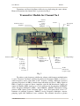
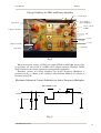
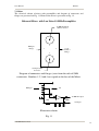
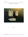
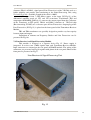
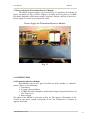
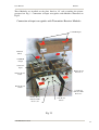
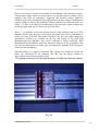
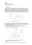
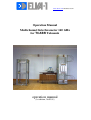
www.elva-1.com [email protected]
Operation Manual
Multichannel Interferometer 140 GHz
for TCABR Tokamak
operation manual
(1st edition, 26.03.98)
User Manual
ELVA-1
1. GENERAL REMARKS
Multichannel Interferometer is intended to be used for measurements of electron
density of plasma in TCABR tokamak. It provides measurements is 3 channels
simultaneously. Channels would be connected to 7 vertical chords. This is entire
plasma diagnostics, that includes all needed components for density measurements.
Output signals of the diagnostic would be stored by data acquisition system of the
tokamak.
140 GHz Interferometer
1
User Manual
ELVA-1
2. PRINCIPLES OF OPERATION
2.1 General description.
The device based on the fact, that phase of millimeter wave signal passed
through plasma depends on electron density averaged along the passing way.
Interferometer measures phase of the signal and provides analog voltages for tokamak
data acquisition system accordingly. Device consists of the following parts:
3 Transceivers of millimeter waves.
Set of Oversized Waveguides.
Two Vacuum Flanges with Built-in Antennas and Vacuum Windows.
Signal Processing unit.
Set of waveguide support elements, chord switches and waveguide high
voltage isolators.
Photo of the entire Interferometer assembled in laboratory conditions is
presented on Fig.1. The device is designed to be installed into standard 19” rack. Rack
is not included into the device.
Assembled Multichannel Interferometer
Oversized
Waveguides
7.2x3.4 mm
High Volatge
Waveguide
Isolators
Vacuum Flanges
for TCABR
Tokamak with 7
antennas and
Vacuum
Windows
Signal
Processing Unit
Flexible
Waveguides
for chords
switching
3 Transceivers
Waveguide
support elements
Fig.1
140 GHz Interferometer
2
User Manual
ELVA-1
There are 3 independent channels designed using the same scheme.
Heterodyne method of the receiving of the signal passed trough the plasma is used.
That allows to achieve good sensitivity and large dynamic range of the device. The
phase of passed signal is measured by the comparing with a phase of signal in
reference channel built-in into each transceiver. Frequencies and output powers for
Transmitters and Local Oscillators for 3 Transceivers are presented in table below:
Table 1.
Number of
Channel
1
1
2
2
3
3
Module
Frequency, GHz
Transmitter
Local Oscillator
Transmitter
Local Oscillator
Transmitter
Local Oscillator
139.0
139.018
140.0
140.018
140.842
140.860
Output Power,
mW
20
12
17.9
16
21
12
There are two main advantages of the scheme which allows to make it more
stable and reduce the problem connected with “phase jumps” - loosing of phase
tracing. First one is a large dynamic range and sensitivity. The system operates
properly up to -85 dB max attenuation between transmitter and receiver. 60 dB
dynamic range is provided. It means that the device properly measure phase of
millimeter wave signal passed through the plasma within attenuation range from 25dB up to -85 dB between transmitter and receiver. The second advantage is an
increasing of the phase scale in 18 times. The system is linear within 18*(2Pi). It is
able to recognize the phase jump on value up to 18*(2Pi). There is no loosing of phase
within this scale.
2.2. One channel design.
Block diagram of one channel is presented on the fig.2. All frequencies are
indicated for channel No.2. The device consists of the following elements:
Millimeter wave power Transmitter including Transistor DRO 7.777777
GHz Oscillator, Power amplifier with integrated 20 dB Directional Coupler,
IMPATT Active frequency Multiplier x18. Output frequency of Transmitter
is 140 GHz;
Receiver including Transistor DRO 7.778777 GHz Oscillator, Power
amplifier with integrated 20 dB Directional Coupler, IMPATT Active
frequency Multiplier x18 and Balanced Mixer. Output frequency of LO is
140.018 GHz;
7 GHz Mixer for Reference channel;
18 MHz Pass Band Amplifier with Limiter Output;
Frequency Divider F/18;
Line Transceiver;
Line Receiver and Signal Processing Unit (SPU);
140 GHz Interferometer
3
User Manual
ELVA-1
Block Diagram of the Interferometer
TRANSMITTER
Transistor
DRO
7.777777 GHz
Power Amplifier
with 20 dB
Directional
800 mW
Coupler
Direct Channel
Ψ1
IMPATT Active
Frequency
Multiplier x18
140 GHz
8 mW Coupled Channel (Ψ1)
Ψ1
Ψ1-Ψ2
7 GHz Mixer
1 MHz
Ψ1+∆Ψ(t)
8 mW Coupled Channel (Ψ2)
Transistor
DRO
7.778777 GHz
800 mW
Power Amplifier Direct Channel
with 20 dB
Directional
Coupler
Ψ2
IMPATT Active
Frequency
Multiplier x18
140.018 GHz
LOCAL OSCILLATOR
Ψ2
Balanced Mixer
with Low Noise
18 MHz
Preamplifier
(Ψ1-Ψ2)+∆Ψ(t)
1
18 ± 2 MHz
Pass-Band
Amplifier with
Limiter Output
4
5
Reference Channel, 1MHz, Ψ1-Ψ2
Line
Transceiver
2
(Ψ1-Ψ2)+∆Ψ(t)/18
Frequency
Divider F/18
1 MHz
Signal Channel, 1MHz, (Ψ1-Ψ2)+∆Ψ(t)/18
3
7
Line Receiver
& Signal
Processing
Unit
Saw-tooth voltage
ADC
Triggering pulses,
1MHz
6
Fig. 2
140 GHz Interferometer
4
User Manual
ELVA-1
Transmitter and Local Oscillator in Receiver are built using the same scheme.
Photo of Transmitter for channel No.3 is presented on Fig.3.
Transmitter Module for Channel No.1
Transistor Power
Amplifier
Transistor DRO
Power
connector
1. +12 V
2. Ground
for ±12 V
3. -12 V
4. +27V
5. Ground
for +27V
Current
Stabiliser for
Active
Frequency
Multiplier
Voltage
Stabiliser for
DRO and Power
Amplifier
Isolator
IMPATT
Active
Frequency
Multiplier
Waveguide
Filter
Output Flange
20 dB
Directional
Coupler output
Fig. 3
To achieve good frequency stability the scheme with frequency multiplication
is used. Transistor oscillator stabilized by Dielectric Resonator (DRO) is used as a
stable frequency source with about 5*10-6 frequency stability. Difference between
operating frequencies of DRO’s installed into transmitter and LO is 1 MHz. Signal of
DRO is applied to input of Power Amplifier with 20 dB Directional Coupler on
output. It amplifies DRO signal up to a level sufficient for the pumping of IMPATT
Active Frequency Multiplier (AFM) - about 500mW…800mW. Waveguide isolator
protects AFM against power reflection from a load. Waveguide filter selects 18th
harmonic of pumping frequency. IMPATT Active Frequency Multiplier converts
pumping signal into millimeter wave radiation. The radiation directed to plasma
140 GHz Interferometer
5
User Manual
ELVA-1
through Oversized Waveguides. It is important, that phase of the signal produced by
AFM is hardly defined by phase of the pumping signal.
To avoid any influence of instability of sources the phase of the signal passed
through plasma is compared with the phase of the reference one. Signals are compared
on IF about 1MHz. Diagrams are presented on Fig. 5. For this aim signals from both
DRO’s in transmitter and in LO modules are mixed on 7 GHz Mixer (see Block
Diagram, Fig.2). The signals directed to the Mixer by means of Directional Coupler to
decrease any influence of external measuring schemes to the frequency of DRO’s.
Intermediate Frequency 1 MHz is obtained in reference channel.
Bandwidth of 18 MHz IF Pass Band Amplifier with Limiter Output
Amplification, dB
0 dB
-3 dB
16
18
20
F, MHz
Fig. 4
140 GHz Interferometer
6
User Manual
ELVA-1
Signal Plots for 18 MHz Bandpass IF Amplifier with Limiter Output,
Frequency Divider F/18 & Line Transceiver
1
18 MHz Preamplifier output (IFIN1 X3)
2
Amplifier with Limiter Output (pin 9 (8) DD7)
3
Line Transceiver Output 1 MHz (Signal Channel, pin 18 (16) DD4)
4
7 GHz Mixer output, Line Transceiver Reference input (REFI X5)
5
Line Transceiver Output 1 MHz (Reference Channel, pin 14 (12)
DD4)
Fig. 5
140 GHz Interferometer
7
User Manual
ELVA-1
To obtain 1 MHz IF in the signal channel for comparing with the reference one
the radiation passed through plasma mixes with LO signal on Balanced Mixer with
Low Noise Preamplifier integrated. It is easy to see that IF is 18 MHz, taking into
account 1 MHz frequency separation between DRO’s and x18 factor of frequency
multiplication. Bandwidth of low noise preamplifier is significantly larger, then 18
MHz. Typical bandwidth of preamplifier used is 7 MHz-2.5 GHz. To reduce the noise
the received signal is filtered within bandwidth 18MHz+/-2MHz (see Fig.4). Then it
is amplified by logarithmic Pass-Band Amplifier with Limiter Output. Fixed
amplitude signal with frequency 18 MHz (diagram No.2 on Fig.5) is directed to
Frequency Divider F/18, that provides 1MHz signal for comparing with reference
channel and so for phase measurements. This signal is directed to Line Transceiver
(diagram No.3 on Fig.5).
The bandwidth of filter 18+/-2MHz chosen as a compromise between speed of
the system and sensitivity. To make the system faster it is needed to increase the
bandwidth, because fast change of phase is equivalent to frequency shift. If this shift is
larger then the bandwidth, signal will be lost, that leads to loosing of phase. On the
other hand noise level depends on the bandwidth of the receiver. The application of
heterodyne method allows to increase the bandwidth up to 4MHz which about 10
times higher then bandwidth normally used in homodyne schemes with the same
sensitivity. 4 MHz bandwidth of the filter installed taking into account possible
frequency shift of DRO due to temperature variations.
Line Transceiver sends reference and measured signals (signal 3 and 5 on Fig.
5) to Signal Processing Unit that would be installed fare from tokamak. Twisted pair
5th category should be used to transmit these signals. It is important that transmission
cable is isolated from Line Transceiver and Line Receiver by means of special
transformers with low capacity between input and output. It is needed to decrease
sensitivity of the system to surrounding electromagnetic noise.
2.3 Phase measurements.
Therefore two signals from each channel of Interferometer are sent to Signal
Processing Unit (SPU): reference signal and measured one. Both signals are square
wave 1 MHz frequency and fixed amplitude. SPU measures difference is a phase
between reference and measured signals. The difference depends on electron density
of plasma. On a fig.2 it is marked as ∆Ψ(t). Scale of this phase is increased in 18
times after Frequency Divider F/18. The phase change on 360 degrees of the signal
passed through plasma (point 1 on Fig. 2) corresponds 20 degrees phase change in
output signal (point 3 on Fig. 2). That allows make the system “jump proved”,
because fast jumps of the phase on the value less 18*(2Pi) not leads to phase loss.
System is linear within 18*(2Pi) scale. Either 2*Pi jumps leads to the loss of phase in
the scheme with not increased phase scale. For the presented scheme the phase loss
would be only after the jump exceeds 18*(2Pi) value.
Phase measurements are memorized in digital form using an external ADC.
Signal Processing Unit provides input signals for ADC. It generates two signals: sawtooth voltage for ADC input and triggering pulses. As mentioned above, the principle
of phase measurements based on the comparing of the phase of received signal with
phase of the signal in reference channel. For this aim the saw-tooth voltage is
produced (see fig. 6). Start of each tooth is triggered by a rise of a pulse taken from
the reference channel, then the fall of each tooth is triggered by a fall of 4th pulse
from reference channel countered from the “start triggering pulse”. As a result the
140 GHz Interferometer
8
User Manual
ELVA-1
phase of saw-tooth voltage is hardly connected with the phase of reference channel. If
one apply the saw-tooth voltage to an input of ADC and will use 1 MHz from signal
channel for the triggering, digitized value will be proportional to the phase. The
triggering of ADC should be provided by the fall of the triggering pulses. If all points
measured by ADC at the triggering time one will put on a display, the picture like
“zebra” will be obtained. Distance between ribs of “zebra” defines a scale of phase.
The scale is 36*Pi in the presented scheme.
Signal Diagrams for Line Transceiver and Signal Processing Unit
Reference signal 1 MHz, CL1
t
Blocking pulse, SWRES1
t
Saw-tooth output voltage, SGN1
7
t
Measured signal 1 MHz, IN1
6
t
Triggering pulses, STR1
t
Fig. 6
140 GHz Interferometer
9
User Manual
ELVA-1
To avoid problems with triggering during tooth falling down time period, each
first triggering pulse after 4-th reference pulse (it triggers the fall of each tooth) is
removed (see Fig.6). It means that the triggering of ADC during the falling down
period of the saw-tooth voltage is prohibited. Triggering pulses are shown on Fig.6
(signal No.6 on Fig.2) as well as saw-tooth voltage (signal No.7 on Fig.2).
3. EXPLOITATION CONDITIONS
operations temperature:
relative air humidity :
primary power:
atmospheric pressure:
+10°…+40° C°
up to 95% at the temperature 30° C°
AC(220±22)V/(50±0.5)Hz
84-112 kPa.
4. SPECIFICATIONS
4.1 Transmitters
4.1.1 Operating frequency range and output power of transmitters:
Number of
Channel
1
2
3
Frequency, GHz
140.842
140.0
139.0
Output Power,
mW
21
17.9
20
4.1.2 Frequency stability 5*10-6
4.1.3 Line width less then 1 kHz.
4.1.4 VSWR of output is no more than 1.25.
4.2 Receivers
4.2.1 Operating frequency range and output power of LO’s:
Number of
Channel
1
2
3
Frequency, GHz
140.860
140.018
139.018
Output Power,
mW
12
16
12
4.2.2 Line width of LO’s less then 1 kHz.
4.2.3 Frequency stability of LO’s 5*10-6
4.2.4 Dynamic range of the receiver, i.e. variations of received signal is 60 dB min.
4.2.5 *Noise factor is < 13 dB.
*measured for IF range 0.5-1.5 GHz
4.3 Entire Interferometer.
4.3.1 Time period of phase measurement repetition is 4 microseconds.
4.3.2 Accuracy of phase measurements +/-5 degrees.
4.3.3 Maximum attenuation between transmitter and receiver not less then 85 dB.
140 GHz Interferometer
10
User Manual
ELVA-1
Number of Channel
1
2
3
Attenuation, dB
85
86
87
4.3.4 Maximum attenuation of the signal in plasma then the system still able to
measure the phase, i.e. dynamic range of the entire system taking into account
attenuation in oversized waveguides, vacuum windows, antennas coupling and
insertion losses in all other elements between transmitter and receiver is not less then
20 dB:
Number of Channel No. 1
Chord
141 GHz
1
32 dB
2
27 dB
3
27 dB
4
27 dB
5
30 dB
6
22 dB
7
29 dB
Channel No. 2
140 GHz
40 dB
37 dB
30 dB
36 dB
34 dB
30 dB
34 dB
Channel No. 3
139 GHz
40 dB
34 dB
35 dB
38 dB
34 dB
32 dB
38 dB
4.3.5 All parameters mentioned above are valid after 30 min warming-up period.
4.3.6 Power consumption is no more than 300 VA.
5. RELIABILITY
5.1. Main time to failure, no less than 5000 h.
5.2. 90% life time, no less than 2 years.
7. TECHNICUL DESCRIPTION
7.1 Transmitters and Local Oscillators
Transmitter and Local Oscillator in Receiver are built using the same scheme.
Photo of Transmitter for channel No.1 is presented on Fig.3. DRO and Power
Amplifier can be repaired only on our factory, so electrical schemes are not presented
in this manual.
The following voltages and current consumption should be provided on Power
connector (see Fig.3):
Contact
Voltage
Current
1.
0.8 A max.
+12 V ±0.5 V,
2.
Ground for ±12 V
3.
100
mA
max.
-12 V ±0.5V,
4.
150 mA max.
+27V ±0.5V,
5.
Ground for +27V
-
140 GHz Interferometer
11
User Manual
ELVA-1
Both devices DRO and Power Amplifier use GaAs field transistors. Negative
voltage applied to gate of the transistor limits drain current. If one apply positive
voltage when the negative one is absent, transistors will be broken. It is important,
that there is an alarm scheme in the stabilizer which protects the transistors against the
wrong order of voltage application.
Electronic scheme of voltage stabilizer for DRO and Power Amplifier is
presented on the Fig.7. Numbers of contacts are indicated on the photo No. 8. Output
positive voltage are regulated by means of transistor 2T819A2. It is installed under the
card on metal base plate and don’t see on the photo. Positive polarity output is
+7VDC. Resistors R1 and R2 would be installed to decrease output voltage to
+5VDC…+6.5VDC for DRO. The value of resistor is adjusted on the factory.
Electrical scheme for voltage stabilizer for DRO and Power
Amplifier in Transmitter and LO modules.
R1
12
R2
2T819A2
1
9
13
11
14
+12V
8k2
AOT 110A
2
7
6
3
1
8
4
5
0.68
2D212A
2
10
15
0.01
510
2k2
142EH3
910
100k
2C133A
150
3
KT816Б
5
-12V
4
110
200
6
7
0.68
KT203Б
1k
8
2D212A
1k2
KC139A
Value of resistors R1 and R2 adjusted on the factory.
Fig. 7
140 GHz Interferometer
12
User Manual
ELVA-1
Voltage Stabilizer for DRO and Power Amplifier
15 (Ground)
14
12 (+7 VDC to
Power Amplifier)
2 (Ground)
13 (+5…+6.5V
to DRO)
1 (Input +12 VDC)
11
10
9
5 (-7V)
6 (-7V)
7 (-7V)
3 (Input -12VDC)
8 (Ground)
4 (Ground)
Fig.8
When the negative voltage -12VDC isn’t applied, LED in AOT110A doesn’t light,
so transistors are closed and IC 142EH3 closes output transistor 2T819A2. Diodes
2D212A protects the scheme against the wrong polarity application.
Electronic scheme of Current Stabilizer for Active Frequency Multiplier is
presented on Fig. 9. Photo of the stabilizer with indicated numbers of contacts is
presented on Fig. 10.
Electronic Scheme of Current Stabilizer for Active Frequency Multiplier
KP142EH5B (7805)
1
1
+27VDC
3
3
30
22
2
Output
1.0
2
2D510A
4
Fig. 9
140 GHz Interferometer
13
User Manual
ELVA-1
Current Stabilizer for Active Frequency Multiplier
2
1
IC of Stabilizer
Variable
Resistor for
Current
Adjustment
4
3
Active
Frequency
Multiplier
Waveguide
Isolator
Fig. 10
140 GHz Interferometer
14
User Manual
ELVA-1
7.2 Mixer
The electrical scheme of mixer with preamplifier and diagram of connectors and
flanges are presented on Fig. 11. Photo of the mixer is presented on Fig. 12.
Balanced Mixer with Low Noise 18 MHz Preamplifier
18 MHz IF Output
SMA Connector
4
RF Input
Flange
1
Local
Oscillator
Flange
2
3
+5V Input SMA
Connector
Diagram of connectors and flanges (view from the side of SMA
connectors. Numbers 1,2,3 and 4 are signed on the box of the Mixer.
LO
RF Input
18 MHz IF output
5kΩ
100Ω
+5V Input
Electronic scheme
Fig. 11
140 GHz Interferometer
15
User Manual
ELVA-1
Balanced Mixer with Preamplifier
Fig. 12
140 GHz Interferometer
16
User Manual
ELVA-1
7.3 18 MHz Pass-Band Amplifier with Limiter Output, Frequency Divider and
Line Transceiver.
These components are designed at a metal plate that has the same size as plate
for LO or for Transmitter. Photo of the block (top view) is presented on the Fig. 14.
Block of 18±2 MHz Pass-Band Amplifier with Limiter Output,
Frequency Divider and Line Transceiver
TR3
X2
18 MHz Pass-Band
Amplifier with
Limiter Output
Bandpass Adjustment (C6)
IF2 input (IFIN X3)
TR
1
TR4
TR2
X1
X5
7 GHz Mixer
X4
Frequency Divider:
Line Tranciever
Card
Fig. 14
18 MHz IF signal from Low Noise Preamplifier comes to the input (pin 3 see
Fig 13.) of the AD811 Operational Amplifier with 20 dB Gain. Inductor L1 and
Capacitor C6 and load Resistor 50Ω forms the bandwidth of the amplifier. One can
change the central frequency of the filter adjusting the C6 capacitor (see photo on
Fig.14). Signal from the L1C6 resonance filter comes throw a Buffer Amplifier VT3
to BNC IF1 Control Plug, placed on the down panel of the Transmitter-Receiver
Module, (X2 Fig.13) and to the input of the AD606 amplifier with Limiter Output.
The AD606 (DD7 Fig.13) provides a hard-limited signal output (see plot 2 Fig.5) with
phase stable within 3° over 70 dB of input signal amplitude variations. The amplifiers
are installed into additional bras box (see Fig.14).
Transformer TR1 and comparator AD9696 (DD1 Fig.13) converts the current
signal from the AD606 differential open collector outputs (pins8 and 9 DD7) to TTL
pulses. This 18 MHz pulses from the comparator (pin 8 DD1) comes to the input (pit
4, DD2) of the 18 times frequency divider made of the 74LS193 (Russian analog is
555IE7) counter (DD2) and 74LS74 (Russian-555TM2) D-Trigger (DD3). Two
140 GHz Interferometer
17
User Manual
ELVA-1
elements (DD4.1 & DD4.2, signal part of Line Transceiver) of the 74LS244 used as a
buffer amplifier and provide data transferring to the Signal Processing Unit, using
Twisted Pair Cable. Available Length of the cable is 100 m.
1 MHz signal from 7 GHz Mixer comes to the input (X5 Fig.13) of the
differential amplifier made of VT1 and VT2 transistors. Transformer TR2 and
comparator AD9696KN (DD5 fig.13) converts the current signal from the Collectors
of the Transistors to TTL pulses. DD4.4 and DD4.5 elements of 74LS244 chip
(Russian analog 555AP5) are a reference part of Line Transceiver. Output plug of the
Line Transceiver (X1 Fig.13) is placed on the down panel of the Transmitter-Receiver
Module.
TR3 and TR4 transformers are specially designed to provide very low capacity
between input and output.
Deposition of elements on Frequency Divider and Line Transceiver card is
presented on Fig.14a.
7.4 Line Receiver And Signal Processing Module.
This module is designed as a separate device Fig. 15. Power supply is
integrated. It receives two 1 MHz signals from each Transmitter-Receiver Module.
Input connectors are situated on the rear panel of LR&SP module. The wiring of the
connectors are presented on Fig.16 together with photo of the rear panel. Photo of the
front panel is presented on Fig.17.
Line Receiver & Signal Processing Unit
Fig. 15
140 GHz Interferometer
18
User Manual
ELVA-1
The Rear Panel of Line Receiver & Signal Processing Unit
GND
Fuse
Line Receiver input plugs
1.
2.
3.
4.
REFH
REFL
SGHI
SGLO
2
1
4
3
Fig. 16
Front Panel of the Line Receiver & Signal Processing Unit
Power Indication
Led
Triggering Pulses for ADC
Output plugs
Power Switch
Sawtooth Voltage Signal
Output Plugs
Fig. 17
140 GHz Interferometer
19
User Manual
ELVA-1
Two 1 MHz signals from the Line Transceiver comes to the input plugs of the
Line Receiver (plugs X1, X2, X3 Fig.16). Transformers TR1-TR6 and comparators
DD1- DD6 converts the REF1-REF3 and SG1-SG3 current signals from the Twisted
Pair Cable to TTL pulses: CL1-CL3 (reference channel) and IN1-IN3 (signal
Channel). Signal Processing Chip (DD7) forms SWRES1-SWRES2 pulses for
Sawtooth Generator control using CL1-CL3 and ADCWR1-ADSWR3 strobes for
ADC triggering (plugs S1-S3 see Fig.18) using IN1-IN3.
Sawtooth Generator is made of Current stabilizer (VT1, VD1, R1, R2
Fig.18), Capacitor C1, Operation Amplifier DD9 and Inverter with open collector
output DD8. If an output transistor of the Inverter is closed (SWRES1=0), the
stabilized current charge the C1 capacitor and voltage on the capacitor grows lineally.
When SWRES1 signal becomes 1, then inverter connect positive plate of C1 to
ground and discharge it. It forms the negative edge of the Sawtooth voltage. Charging
current is determined by the value of the Sawtooth Amplitude Adjustment Resistors
(see Fig.18) R2. Voltage Applied to the emitter of the VT1 transistor is stabilized
using the VD1 reference. Adjusting the Value of R2 one can install the desired
amplitude of the output Sawtooth Voltage. Sawtooth signal from the C1 capacitor
comes through the buffer operational amplifier DD9 to the R1 Sawtooth Voltage
Signal Output Plug (see Fig.18).
Scheme of elements deposition on the card of Line Receiver And Signal
Processing Module is presented on Fig.19. Photo of Module with removed upper
cover is presented on Fig.20.
Local power supply made of Transformer TR1, Diodes VD2 and VD3 and
stabilizers 7805 and 7905 provide stabilized ±5 V voltages.
Disposition of Elements & Blocks In the Line Receiver & Signal
Processing Module
Primary Power
Transformer TR7
Sawtooth Amplitude
Adjustment Resistors
(channel No. 1; 2; 3)
Sawtooth Voltage
Generator (channel 3)
Line Receiver
Input Plugs
Sawtooth Voltage
Generator (channel 2)
Local Power
Stabilizer
Sawtooth Voltage
Generator (channel 1)
Line Receiver
Input
Comparators
Signal Processed
Chip
Line Receiver Input
Transformers
fig. 20
140 GHz Interferometer
20
User Manual
ELVA-1
7.5 Power Supply for Transmitter-Receiver Module.
The scheme of power supply is presented on Fig. 21, deposition of elements on
Fig.22 and photo on Fig.23. Power Supply is installed under the plate of 18 MHz
Pass-Band Amplifier with Limiter Output, Frequency Divider and Line Transceiver.
Power supply is covered by metal plate for safety.
Power Supply for Transmitter-Receiver Module
Fig. 23
8. CONSTRUCTION
8.1 Transmitter-Receiver Modules
Each Module consists of 4 plates installed one under another at “sandwich”
manner. Plates are the following:
1. Transmitter,
2. LO with connected Mixer,
3. 18 MHz Pass-Band Amplifier with Limiter Output, Frequency Divider and
Line Transceiver,
4. Power Supply
The photo of the Module is presented on Fig. 24. The output of Transmitter is not
viewed on the photo. Output vaweguides of LO and Transmitter is installed in
opposite directions.
140 GHz Interferometer
21
User Manual
ELVA-1
Three Modules are installed on the plate fitted to 19” rack according the picture
presented on Fig. 1. Connection of input waveguides with Modules illustrated on
Fig.25.
Connection of input waveguides with Transmitter-Receiver Modules
2 mm RF Inputs
Balanced
Mixer
18 MHz IF
Output
+5V Power
Input
Primary Power
Fuse 0.5 A
Primary Power
Cable
Primary Power
Switch
+12V Power
Indicator LED
Red color
Primary Power
Indicator LED,
Green color
+12V Power
Switch
Fig. 25
140 GHz Interferometer
22
User Manual
ELVA-1
There are two power switches are installed on each Module. One switch for negative
voltage power supply and the second switch is for all other positive voltage power
suppliers. The order of switching is important. The negative voltage should be
switched on first and switched off last. Application of positive voltage is prohibited if
negative voltage is absent. The problem is connected with GaAs field transistors (see
article 7.1). There is an alarm system that protects the transistors against wrong order
of voltage application, but it is better not use it too often.
There is a possibility to measure plasma density along different chords of TCA
tokamak. For this aim the peace of oversized waveguide connected to Transmitter or
to Receiver made bent and. That make it flexible a bit. Two waveguide connectors
(mechanical switches) are installed on the top and bottom of the rack with
Transmitter-Receiver Modules. One of the connector is shown on Fig.26. Each
Transmitter-Receiver Module would be connected with one of five waveguides. For
this aim one should unscrew fixing plate and change the position of the waveguide
connected with the Module.
Tokamak flanges are supplied assembled. The vacuum test should be carried out
before the installation to the tokamak. For this aim the flanges should be
disassembled, cleaned and assembled again.
Waveguide connector for the measurements in different tokamak chords
Fig. 26
140 GHz Interferometer
23