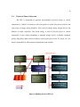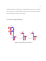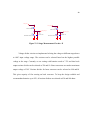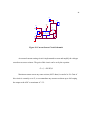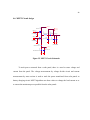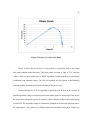
1
ABSTRACT
SHAH, MIHIR ROHIT. Enabling Aggressive Voltage Scaling for Real-Time and Embedded
System with Inexpensive and Efficient Power Conversion. (Under the direction of Dr.
Subhashish Bhattacharya).
The thesis takes Electrical Power Subsystem (EPS) for CubeSats as a base and builds
the concept of Aggressive Voltage Scaling with Real Time Implementation using it. EPS is
flexible, scalable and reconfigurable for its use in wide range of small satellites with different
power processing requirements. It consists of battery charging modules to store solar energy
and point of load modules to use it to power other subsystems and payloads. The thesis
discusses the requirements, specifications, architecture and implementation of EPS. It also
discusses various protection and failure recovery features making the subsystem robust in the
harsh space environment. Software implementation and RTOS based implementation are
reported which apply algorithms like MPPT and PID to the converters of the subsystem. A
prototype board is developed and results are presented. The effect of change in control loop
frequency on load transients is discussed. This helps to lower the cost of system by relaxing
the real-time requirements and enabling the use of low end micro controllers or designing
multiple subsystems using a single micro controller. Aggressive Voltage Scaling method
processes the power supplied to the loads and keeps it to a minimum by scaling the supply
voltage based on the state of loads. These concepts can be applied to a variety of embedded
system power supplies with wide range of power requirements.
The thesis also reports the use of GaN devices for power converters. eGaN devices
from EPC rated at 200V, 12A are used to develop a prototype board with gate driver circuit
for the devices. The devices are switched at up to 1.5MHz with the output current of 1A at
50V. A prototype board using off the shelf gate drivers is also designed to compare its
performance with the prototype with indigenous gate driver circuit.
© Copyright 2012 by Shah Mihir Rohit
All Rights Reserved
Enabling Aggressive Voltage Scaling for Real-Time and Embedded System with Inexpensive
and Efficient Power Conversion
by
Mihir Rohit Shah
A thesis submitted to the Graduate Faculty of
North Carolina State University
in partial fulfillment of the
requirements for the degree of
Master of Science
Computer Engineering
Raleigh, North Carolina
2012
APPROVED BY:
___________________________
Dr. Subhashish Bhattacharya
Chair of Advisory Committee
__________________________
Dr. Srdjan Lukic
__________________________
Dr. Alexander G. Dean
ii
DEDICATION
TO
MY PARENTS
RASHMITA SHAH & ROHIT SHAH
MY SISTER
SWATI SHAH
AND MY FIANCÉE
NIDHI JOSHI
iii
BIOGRAPHY
Mihir Shah was born on April 20, 1986 in Ahmedabad (Gujarat), India. He did his schooling
from Shri C. C. Shah Sarvajanik English High School, Surat. He received the degree of Bachelor of
Technology in Electronics Engineering from National Institute of Technology, Surat, India in 2008.
He started pursuing his graduate studies in the field of Computer Engineering at North Carolina State
University in Spring 2011. He is associated as a student with Future Renewable Electrical Energy
Delivery and Management (FREEDM) Systems Center during his study at North Carolina State
University. He is engaged in research in application of embedded systems in the field of power
electronics. His interests span across a wide range of subjects – Embedded Systems, Digital Design,
Computer Architecture and Power Electronics.
Mihir has been an entrepreneur and has developed and marketed products and provided
consultancy in the field of embedded systems during his undergraduate program, from 2006 to 2008.
From 2008 to 2010, he worked as Design and Development Engineer at Tata Elxsi Ltd., India. He has
worked in the field of Digital TV and Multimedia Systems, Image Processing, Video Analytics and
Computer Architecture. He has developed Automated Testing Environment (ATE) for Multimedia
Home Platform on Sony Bravia, Ground Truth Video Analytics Tool for Canon cameras and
benchmarked Intel’s SandyBridge Processor against its predecessors. From May 2012, he has been
working as an Intern in IBM, where he is involved in the development of Hardware Acceleration for
Internet Scale Messaging and Cloud Computing Servers.
iv
ACKNOWLEDGEMENTS
I express my sincere gratitude and thank my advisor, Dr. Subhashish Bhattacharya for
the support and guidance he has provided during my graduate program at North Carolina
State University. His belief in me and constant encouragement made this Masters program a
fruitful experience. He has been a source of inspiration, in both personal and professional
domains. I thank my committee, Dr. Alexander G. Dean and Dr. Srdjan Lukic, for providing
valuable feedback and continuous support during this project. I thank FREEDM Systems
Center for sharing the resources and National Science Foundation for funding this project. I
thank Avik Juneja, Tharunachalam Pindicura and Michael Plautz, for working with me to
accomplish this project.
I am grateful to Shailesh Notani, for introducing me to Dr. Bhattacharya and this
project. I appreciate the valuable inputs and discussions by my seniors and friends, Kamalesh
Hatua, Arun Kadavelugu, Samir Hazra, FNU Sachin Madhusudan, Hesam Mirzaee, Awneesh
Tripathi and Sumit Datta at FREEDM Systems Center. I extend my gratitude towards the
staff members of the center, especially Karen Autry and Colleen Reid for the facilities and
support. I thank Hulgize Kassa for his supervision assuring my safety in the laboratory.
I would like to thank my friends Chintan Panirwala, Nikunj Bhansali, Aarohi Patel,
Milind Kulkarni, Komal & Jayesh Bhambhani, Amit Deshmukh, Sushant Sinha, Prathamesh
Save, Jaydip Solanki, Hemil Jariwala, Richa Asarawala, Nidhi Pandya, Shikhar Singh,
Bharat Balagopal, Bharath Balasubramanian and Abhinaya Nakka for being my family
during the stay at North Carolina State University and making it a joyful journey.
v
Finally, I would like to thank my parents, Rashmita Shah and Rohit Shah and my
sister, Swati Shah for their care and constant support and my fiancée, Nidhi Joshi for her love
and patience.
vi
TABLE OF CONTENTS
LIST OF FIGURES .................................................................................................................................. viii
LIST OF TABLES ....................................................................................................................................... x
CHAPTER 1 Introduction ......................................................................................................................... 1
CHAPTER 2 CubeSat ................................................................................................................................ 5
2.1.
Introduction ............................................................................................................................ 5
2.2.
CubeSat Specifications ........................................................................................................... 9
2.3.
CubeSat Subsystems:............................................................................................................ 10
2.3.1.
Attitude Determination and Control Subsystem (ADCS) .............................................. 11
2.3.2.
Command and Data Handling (CDH) Subsystem .......................................................... 12
2.3.3.
Communication (COM) ................................................................................................. 12
2.3.4.
Electrical Power Subsystem (EPS)................................................................................. 12
2.3.5.
Structures (STR) ............................................................................................................ 13
2.3.6.
Payload (PLY) ................................................................................................................ 13
2.3.7.
Software ....................................................................................................................... 13
2.4.
Electrical Power Subsystem.................................................................................................. 15
CHAPTER 3 Previous Work ................................................................................................................... 18
3.1. Clyde Space EPS ......................................................................................................................... 18
3.2. CubeSat Kit EPS.......................................................................................................................... 20
3.3. CubeSat EPS ............................................................................................................................... 22
3.3.1. Design Specifications .......................................................................................................... 22
3.3.2. Proposed Architecture ....................................................................................................... 25
CHAPTER 4 Hardware Design and Modifications ................................................................................. 28
4.1. Flexible Battery Charging Module ............................................................................................. 32
4.2. FDPOL ........................................................................................................................................ 34
4.3. Path Selection ............................................................................................................................ 37
4.4. Power Failure & Recovery ......................................................................................................... 38
4.5. Current & Voltage Measurement .............................................................................................. 39
4.6. MPPT Circuit design ................................................................................................................... 42
vii
4.7. Controller................................................................................................................................... 43
4.8. TestBed ...................................................................................................................................... 45
CHAPTER 5 Software Design ................................................................................................................. 48
5.1. Controller Software Design ....................................................................................................... 48
5.1.1. Board Driver ....................................................................................................................... 48
5.1.2. Control Loop ....................................................................................................................... 50
5.1.3. Debug Interface .................................................................................................................. 52
5.2. RTOS based implementation ..................................................................................................... 52
5.3. Communication and Configuration Design ............................................................................... 55
5.4. MPPT Algorithm Implementation ............................................................................................. 56
5.5. PID Control of POL converters ................................................................................................... 59
CHAPTER 6 Aggressive Voltage Scaling ................................................................................................ 63
CHAPTER 7 Results ............................................................................................................................... 67
7.1.
FBCM .................................................................................................................................... 67
7.1.1.
Open Loop .................................................................................................................... 67
7.1.2.
Closed Loop .................................................................................................................. 69
7.2.
FDPOL ................................................................................................................................... 71
7.2.1.
Open Loop .................................................................................................................... 71
7.2.2.
Closed Loop .................................................................................................................. 73
CHAPTER 8 High Frequency GaN device based implementation ......................................................... 74
8.1. GaN based phase leg with indigenous driver circuit ................................................................. 77
8.1.1. Circuit.................................................................................................................................. 77
8.1.2. Board Layout ...................................................................................................................... 79
8.1.3. Results ................................................................................................................................ 80
8.2. Development of GaN based circuit with LM5113 driver IC ....................................................... 84
8.2.1. Results ................................................................................................................................ 85
CHAPTER 9 Summary and Future Work ............................................................................................... 87
REFERENCES ......................................................................................................................................... 89
viii
LIST OF FIGURES
Figure 1. SMART-1 Swedish Medium Sized Satellite........................................................................... 6
Figure 2. One mini satellite of RapidEye Constellation ......................................................................... 7
Figure 3. AENEAS – A 3U CubeSat ..................................................................................................... 8
Figure 4. P-POD Deployer .................................................................................................................. 10
Figure 5. CubeSat Subsystems ............................................................................................................. 11
Figure 6. Building blocks of EPS ........................................................................................................ 15
Figure 7. Architecture of Clyde-Space EPS ........................................................................................ 18
Figure 8. Clyde Space EPS Hardware .................................................................................................. 19
Figure 9. Architecture of CubeSat Kit EPS .......................................................................................... 20
Figure 10. CubeSat Kit EPS Hardware ................................................................................................ 21
Figure 11. Proposed Architecture for CubeSat EPS ............................................................................. 25
Figure 12. Hardware Implementation of EPS ...................................................................................... 28
Figure 13. EPS Prototype Board Sections ............................................................................................ 29
Figure 14. EPS Prototype Board .......................................................................................................... 30
Figure 15. Current Sensing Board ........................................................................................................ 30
Figure 16. EPS Board with Current Sensing Board ............................................................................. 31
Figure 17. Flexible Battery Charging Module Schematic .................................................................... 33
Figure 18. Flexible Digital Point of Load – Buck Converter Schematic.............................................. 35
Figure 19. Flexible Digital Point of Load – Boost Converter Schematic............................................. 36
Figure 20. Path Selection Feature Schematic ....................................................................................... 37
Figure 21. Power Failure Recovery Circuit Schematic ........................................................................ 38
Figure 22. Voltage Measurement Circuits - I ....................................................................................... 39
Figure 23. Voltage Measurement Circuits - II...................................................................................... 40
Figure 24. Current Sensor Circuit Schematic ....................................................................................... 41
Figure 25. MPPT Circuit Schematic .................................................................................................... 42
Figure 26. Micro Controller Interface Schematic................................................................................. 43
Figure 27. Micro controller Kit interface circuit .................................................................................. 44
Figure 28. Micro controller Kit interface board ................................................................................... 45
Figure 29. TestBed ............................................................................................................................... 46
Figure 30. FBCM Over Current Situation ............................................................................................ 51
Figure 31. RTOS based implementation .............................................................................................. 53
Figure 32. Configuration and Debugging Interface.............................................................................. 55
Figure 33. V-I characteristics of Solar Panel........................................................................................ 56
Figure 34. Power Curve for Solar Panel ............................................................................................... 57
Figure 35. Open loop response of servo motor .................................................................................... 60
Figure 36. Closed loop response for interrupt driven implementation (Load: Servo Motor)............... 60
Figure 37. Closed loop response for RTOS based implementation (Load: Servo Motor) ................... 61
ix
Figure 38. Response time based on control loop frequency ................................................................. 64
Figure 39. Selection of Control loop update rate based on Voltage Margin ........................................ 65
Figure 40. FBCM – Boost Mode .......................................................................................................... 68
Figure 41. FBCM – Buck Mode ........................................................................................................... 68
Figure 42. FBCM – Closed Loop Control ............................................................................................ 69
Figure 43. FDPOL converters at 75% and 25% duty cycles ................................................................ 71
Figure 44. FDPOL converters at 50% duty cycle................................................................................. 72
Figure 45. FDPOL converters – varying duty cycle on the fly ............................................................ 72
Figure 46. FDPOL Closed Loop Control ............................................................................................. 73
Figure 47. Resistance vs Breakdown Voltage comparison .................................................................. 75
Figure 48. LGA Package for EPC eGaN devices ................................................................................. 76
Figure 49. Digital and Power Section Schematic for GaN board......................................................... 77
Figure 50. Isolated power supply circuit for gate driver ...................................................................... 78
Figure 51. GaN device based Phase Leg - Board Layout ..................................................................... 79
Figure 52. Low Power Buck Converter at 1.5MHz.............................................................................. 80
Figure 53. High Power Buck Converter at 1MHz ................................................................................ 81
Figure 54. Low Power Boost Converter at 1MHz ................................................................................ 82
Figure 55. High Power Boost Converter at 1MHz ............................................................................... 82
Figure 56. GaN based phase leg circuit using LM5113 ....................................................................... 84
Figure 57. Board layout - GaN based phase leg using LM5113 .......................................................... 85
Figure 58. GaN based buck converter using LM5113 at 2MHz........................................................... 86
x
LIST OF TABLES
Table 1. Solar Cell Configurations ....................................................................................................... 23
Table 2. File Structure for Driver Code................................................................................................ 48
1
CHAPTER 1
Introduction
Embedded systems have become an integral part of our life. Right from an electronic
tooth brush to a mobile phone or an unmanned surveillance robot to a satellite, embedded
systems have played a crucial role in making tasks efficient and easy. Embedded systems are
developing at an unprecedented rate in terms of features, capability and power. With the cost
of high performance hardware going low and with the aid of easily available development
tools, the overall cost and development time of each system is decreasing.
An increasing number of devices are going portable these days. These devices operate
on battery power and are getting smaller in size. With increasing portability comes the
challenge of designing efficient battery systems. The devices are made up of multiple
subsystems designed to perform specific tasks. With more number of devices going portable
and complex, there is a need for efficient power subsystems that can be embedded in these
devices. The power subsystem should be able to provide power for the entire embedded
system which includes charging the batteries and using the energy stored in the batteries to
power the subsystems. The power subsystem should be low cost, efficient and easily
reconfigurable for various applications. It should generate multiple voltage domains so as to
eliminate the need for each subsystem to have its own power converter. Increasing the
efficiency of the device by reducing the number of power conversion stages is critical. The
2
devices go into a low power or standby mode when not in use to save power consumption.
Generally, the low power mode is achieved by reducing the frequency of operation of
subsystems. The system can operate at low voltage in standby mode. Power being directly
proportional to the square of voltage, scaling the supply voltage of the system saves a
significant amount of power. The motivation of the project is to develop a low cost, efficient
and scalable power subsystem which can aggressively and intelligently scale the output
voltage on multiple rails to reduce power consumption of the system.
CubeSat is a very good example of an embedded system with stringent voltage and
power limits of operations. It is a battery powered system which has communication
capabilities and high performance sensing equipment like earth imaging and weather
monitoring equipment. It has a dedicated Electrical Power Subsystem (EPS) which serves as
the power processing and regulating subsystem. The size and weight constraints of CubeSat
along with its power processing requirements make EPS design very critical.
3
CHAPTER 2 describes CubeSat mission, satellite specifications and various
subsystems. It also discusses EPS in detail.
CHAPTER 3 discusses previous work in the field of development of CubeSat EPS. It
discusses the architecture, implementation, advantages and drawbacks of various CubeSat
Electrical Power Subsystems available in the market. It is followed by the work [1] by
Shailesh Notani. He gathered design specifications for EPS, proposed architecture which
caters the requirements and developed prototype board. He has reported preliminary test
results of the prototype board. Testing of high frequency GaN devices, development of phase
leg and its results are discussed in [1]. This thesis is based on his work. Enhancement of EPS
prototype board (CHAPTER 4), software design and implementation (CHAPTER 5),
communication and debugging interface (CHAPTER 5) and enhancement and redesign of
GaN devices based phase leg along with implementation of buck and boost converters using
the phase leg (CHAPTER 8) is discussed in as a part of the work in this thesis. Aggressive
Voltage Scaling, its requirements and advantages are discussed in CHAPTER 6.
Being a part of the project team, I was responsible for developing and implementing the
following mentioned segments.
•
Testing the CubeSat EPS board
•
Modifications in FBCM and FDPOL circuits
•
Modifications in path selection feature circuit and power failure circuit
•
Design of breakout board to interface EPS board with any micro controller development
kit
4
•
Design and development of Current Sensing circuit for EPS
•
Software development – board driver and interrupt driven control implementation
•
Communication and Debug Interface
•
Plugging PID algorithm in interrupt driver control implementation for point of load
converters
•
MPPT algorithm implementation
•
Over-current and under-voltage protection implementation
•
Enabling the EPS board for Aggressive Voltage Scaling implementation
•
A part of Aggressive Voltage Scaling implementation
•
Enhancement and re-design of GaN devices based phase leg
•
Development and testing of buck and boost converters using the phase leg
The test bed discussed in Section 4.8., developed by Michael Plautz, an MS student
under Dr. Alexander Dean, is used to test the EPS and characterize various loads and their
transients. The CubeSat EPS board is used to test various implementations. RTOS based
implementation discussed in Section 5.2. and implementation of PID on RTOS discussed in
Section 5.5. are developed by Avik Juneja and are tested on EPS board.
5
CHAPTER 2
CubeSat
2.1.
Introduction
The term “CubeSat” is used for satellites that adhere to the standards described in
CubeSat design specification. The program is led by Professor Jordi Puig-Suari at California
Polytechnic State University, San Luis Obispo and Professor Bob Twiggs at Stanford
University’s Space System Development Laboratory with an aim to design a satellite with
capabilities that a graduate student could design, build, test and operate. Its primary purpose
was to reduce cost, decrease development time and increase number of experimental
launches. It also aimed to increase collaboration between universities and private companies
to build small satellites.
Satellites can be classified on the basis of their size/weight:
•
Large Satellite: Wet Mass greater than 1000kg
•
Medium Sized Satellite: Wet Mass between 500-1000kg
•
Mini Satellite: Wet Mass between 100-500kg
•
Micro Satellite: Wet Mass between 10-100kg
•
Nano Satellite: Wet Mass between 1-10kg
•
Pico Satellite: Wet Mass between 0.1-1kg
•
Femto Satellite: Wet Mass less than 100g
6
These definitions are not strict but are general. They are sometimes cross-referred
based on their size and weight. This thesis deals with power system design for CubeSats
which fall under the category of Pico Satellites and Nano Satellites.
Figure 1. SMART-1 Swedish Medium Sized Satellite
The satellite SMART-1 was a Swedish designed ESA mini satellite weighing 367kg
that orbited around the moon for three years after its launch in September, 2003 until it was
deliberately crashed into the Moon’s surface in September 2006 to study the effect of a
meteor impact and expose materials in the ground to spectroscopic analysis.
7
Figure 2. One mini satellite of RapidEye Constellation
RapidEye constellation is an example of distributed tasks mini satellites where a
group of 5 identical satellites weighing 150kg each is employed to perform imaging task on
the earth. These satellites have sensors that assist in monitoring vegetation health, improve
species separation and help in measuring protein and nitrogen content in biomass. These
satellites are to be replaced with a group of 6 micro satellites weighting 38kg to improve the
revisit time of 3.5 hours as compared to 24 hours.
On August 2, 2012 Atlas V rocket launched from Vandenberg Air Force Base in
California deployed 11 CubeSats for US Government and NASA ELaNa university program
[2]. These satellites are:
•
CINEMA by University of California at Berkeley: A 3U cubesat to study Space
Weather effects in near-Earth Space.
•
CSSWE by University of Colorado at Boulder: A 3U cubesat to study the relationship
between solar flares and energetic particles.
8
•
CP5 by California Polytechnic State University at San Luis Obispo: A 1U cubesat
De-Orbiting experiment using a Deployed Thin-Film Mechanism.
•
CXBN by Morehead State University: A 2U cubesat Map the entire sky in X-ray
spectrum using energy cosmic background radiation measurements in the 30-50KeV
range.
•
Aeneas by University of Southern California: A 3U cubesat to prove the concept of
wifi based tag tracking from low earth orbit to track cargos in the open ocean waters.
•
ORSES by Operationally Responsive Space Office: A 3U cubesat for US Army
Space and Missile Defense Command.
•
HORUS & RE by Lawrence Livermore National Laboratory: Both 3U CubeSat to
detect orbiting payloads and debris for orbital measurement
•
Aerocube 4A, 4B, 4C by Aerospace Corporation: For technical research
Figure 3. AENEAS – A 3U CubeSat [3]
9
Five CubeSat were deployed from the International Space Station on October 4, 2012.
These CubeSats were carried to ISS by a Japanese HTV cargo carrier and they have payloads
[4] - Morse code communication with the earth using LED – optical interface, a ham radio
transmitter, space photography, infrared photography and earth observation. This
demonstration proved the concept of deployment of cubesats from a bigger satellite like
International Space Station.
Looking at the current trends, it is seen that the shift to the CubeSat specification for
satellite development has increased the frequency of cubesats being deployed. More number
of missions is being planned as these are low-cost and fast to develop missions.
2.2.
CubeSat Specifications
A CubeSat is a 10 cm cubed sized small satellite with maximum mass of 1.33kg.
These are known as 1U (one unit) CubeSats. They can be scaled in one axis in increments of
1U modules to make 2U CubeSats (20cm x 10cm x 10cm) and 3U CubeSats (30cm x 10cm x
10 cm). This standard 10cm x 10cm size enables the use of common deployment system thus
reducing the cost of development of deployment system.
10
Figure 4. P-POD Deployer [5]
Cal Poly has developed Poly Picosatellite Orbital Deployer (P-Pod) [5] [6] which
carries the CubeSats into the orbit and deploys them. P-POD Mk III [7] has the capability to
deploy a 3U CubeSat or a combination of 1U and 2U CubeSats sizing up to 3U CubeSats.
Cal Poly has a CubeSat Acceptance Checklist [5] which needs to be fulfilled for a CubeSat to
be deployed by P-POD. P-PODs have been used to deploy all the CubeSats since 2006.
Along with the size constraints, a CubeSat is required to fulfill vibration standards, radiation
hardness standards, launch procedures and other design requirements like deployment
switches and launch pins.
2.3.
CubeSat Subsystems:
A CubeSat comprises of following subsystems [8]:
11
Figure 5. CubeSat Subsystems
2.3.1.
Attitude Determination and Control Subsystem (ADCS)
The Attitude Determination and Control Subsystem (ADCS) [9] keeps the satellite in
proper orbit and orientation. It consists of a permanent magnet to stabilize the satellite about
earth’s magnetic field. It possesses sensors like magnetometer to determine the satellite’s
orientation and send it to Control and Data Handling subsystem, sun sensors to detect the
direction of sun and accelerometers to detect the motion of satellite. Actuators like Hysteresis
rods providing magnetic damping, momentum wheels, etc. are present in the subsystem to
prevent oscillation about the spinning axis and correct the attitude of satellite. The subsystem
is responsible to point the antenna in an orientation to establish a good communication with
the ground station, the solar panels towards the sun and the imaging camera towards the
earth.
12
2.3.2.
Command and Data Handling (CDH) Subsystem
The Command and Data Handling (CDH) system is the brain of the satellite. It is
responsible to control all other subsystems, provide communication with ground station,
store and process data from sensors and detect and manage faults. This subsystem
communicates with all other subsystems and maintains their operation along with providing
communication interface between subsystems and ground station.
2.3.3.
Communication (COM)
The Communication (COM) system is responsible for providing the data link
between the Command and Data Handling (CDH) system and the ground station to
communicate control commands as well as receive health and status data through a bidirectional, full duplex communication system. The COM system is made up of three main
components: the antenna design, the terminal node controller (TNC), and the
radio/transceiver. The communication functionalities like data rate control; flow control and
standby/shutdown are controlled by Command and Data Handling (CDH) subsystem.
2.3.4.
Electrical Power Subsystem (EPS)
The Electrical Power Subsystem (EPS) is responsible to regulate power supply to all
subsystems. It is interfaced with the solar panels to harness the solar power and with batteries
to store the energy. This stored energy is used to provide electrical power to other
subsystems. It possesses the ability to regulate and respond to conditions like no power, over
current, etc. but it is primarily controlled by Command and Data Handling subsystem. The
thesis deals with EPS in detail.
13
2.3.5.
Structures (STR)
All subsystems, circuits and payloads are safely housed in the CubeSat structure. It
provides mounts and supports so that all subsystems can be mounted. It is responsible to
provide protection from the space environment and radiation. The structure is the interface
between the CubeSat and deployer. It can slide on the rails to be easily deployed by the
springs mounted on the deployer. It has the deployment switches which senses separation
from the deployer.
2.3.6.
Payload (PLY)
Payload consists of experiments, proof of concept designs, individual tasks like
imaging or distributed tasks like weather monitoring. With the continued advances in
miniaturization and capability increase of electronic technology, it is possible for small but
complicated tasks like imaging to be accomplished by a system as small as a CubeSat.
Payload and its application are used to create specifications for all the other subsystems of
the satellite.
2.3.7.
Software
The software is divided into two categories. The ground station software is
responsible to communicate with the satellite and display status of the satellite along with
payload experimental data to ground crew. Flight software is responsible for the control and
operations of CubeSat. It should support various modes like communications mode, idle
mode and power save mode along with handling emergency conditions that arise during the
flight. All subsystems should communicate smoothly for successful operation of satellite.
14
EPS should have algorithms for maximum power point tracking, battery health monitoring,
PID controls and voltage scaling. Refer later chapters for further discussion on EPS software.
15
2.4.
Electrical Power Subsystem
The EPS is responsible to generate and distribute electrical energy to various
subsystems in CubeSat. It interfaces with solar panels to extract solar power which is the
only source of energy during operation. This is used to charge energy storage devices like
batteries or super capacitors. The stored energy is used to provide power to various
subsystems. It runs various algorithms to maintain storage devices in healthy condition,
protect subsystems under electrical failures, extract peak power from PV arrays, etc. It is
directly responsible for efficient power distribution in the satellite.
Regulated Power Bus
Storage-Lithium
Batteries
Point Of Load Module
(FBCM)
Communication System
Flexible Battery
Charging Module
(FBCM)
Payload
Flexible Digital
Point of Load DC/DC (FDPOL)
Command & Data
Handling
Central Digital Power
Controller
Solar Panel Panels
Attitude Determination
& Control System
Figure 6. Building blocks of EPS [1]
16
Figure 6 shows the general architecture of EPS with the essential blocks of the
subsystem. Here, Flexible Battery Charging Module (FBCM) derives energy from solar
panels and stores it in Li batteries. Flexible Digital Point of Load (FDPOL) Converter is
responsible to generate a regulated power bus which powers other subsystems and payloads.
In the absence of battery power, point of load converter can extract the power from the solar
panels as well. The Central Power Controller controls FBCM and FDPOL and runs various
health and protection algorithms. It communicates with Command and Data Handling (CDH)
Subsystem to receive commands regarding the system. It is to be noted that subsystems
possess power converters to convert power bus to their power requirements. As each
subsystem needs to have its own power converter, the electrical efficiency of the satellite
reduces.
This helps us to note the requirements of Electrical Power Subsystem:
•
It should be low cost and efficient.
•
It should have multiple point-of-load converters to generate various power rails to cater
power requirements of multiple payloads.
•
It should be flexible to accommodate a variety of specifications and configurations of
solar panels as well as the batteries.
•
It should be scalable to cater the needs of 1U to 12U CubeSats.
•
It should be reconfigurable to eliminate the need for redesigning the power system for
each CubeSat.
17
•
It should be able to handle various load transients generated by subsystems switching to
low power modes and high power modes.
18
CHAPTER 3
Previous Work
The work done in development of CubeSat EPS by Shailesh Notani is reported in his
thesis [1]. First we will look at a few very well-known EPS providers and their architectures
followed by a discussion of the work by Shailesh Notani.
3.1. Clyde Space EPS
Figure 7. Architecture of Clyde-Space EPS [10]
19
Clyde Space is the world leading supplier of power system components for CubeSats.
They have been designing, manufacturing, testing and supplying power system electronics,
solar panels and batteries for space programmes since 2006. Figure 7 shows architecture of
the second generation of Clyde Space CubeSat Electronic Power System [10] [11]. It
connects to solar panels via Battery Charge Regulators. Each BCR can be connected in
parallel to two solar panels on the opposite faces of the Cubesat. The BCRs have in built
Maximum Power Point Tracker (MPPT) to track the panel which is directly illuminated and
track its maximum power point. This energy from solar panel is used to charge batteries or
provide power to distribution modules via a switched network. The output of the distribution
modules is an unregulated Battery Voltage Bus, a regulated 5V supply Bus and a regulated
3.3V supply Bus. Protections features like Over-Current Bus Protection and Battery Under
Voltage Protection are implemented. EPS communicates with other modules using I2C
telemetry.
Figure 8. Clyde Space EPS Hardware
20
Clyde Space EPS has the output voltage buses limited to 3.3V and 5V. These buses
are non configurable. Thus a subsystems needs to have its own converter if it operates at a
voltage level other than 3.3V or 5V. Also, as the buses are not configurable, they cannot be
switched to lower voltage levels when the subsystems enter low power modes.
3.2. CubeSat Kit EPS
Figure 9. Architecture of CubeSat Kit EPS
21
CubeSat Kit EPS [12] is a product by Pumpkin © Inc. They have been designing the
kit since 2003 and they have the fourth generation of CubeSat EPS in market. CubeSat Kit
EPS uses linear voltage regulators to generate voltage rails of 3.3V and 5V along with
unregulated battery power rail. Use of linear regulators reduces switching noise but reduces
the efficiency of the converters.
Figure 10. CubeSat Kit EPS Hardware
The batteries are charged via USB connector. EPS boards can be stacked to increase
the output current. It has auto-resettable current fuse for over current protection. The kit
provides EPS telemetry via I2C interface. It uses iPod® batteries and there is no interface
with solar cells for charging battery.
22
3.3. CubeSat EPS
In his work [1], Shailesh Notani gathered requirements and design specifications. He
proposed a scalable architecture for EPS and modeled the system. He explored the use of
Rad-Hard GaN devices and discussed its use for CubeSat EPS. He developed a prototype, did
some preliminary tests and presented results for both boards. Here we discuss about his work
and proposed enhancements.
3.3.1. Design Specifications
The paper [1] gathers specifications for solar panels, payloads and various subsystems
of CubeSat to design requirements of EPS. The EPS prototype does not fulfill to all the
requirements as the primary motive is to enable its fast development. Due to rapid
technological advancements various new systems are being deployed in CubeSats along with
new experiments. Thus, EPS needs to be easily scalable and reconfigurable to accommodate
changes in configurations and designs.
Configuration of solar panels depends on batteries being used in the system which in
turn depends on payloads of system. Based on the specifications of battery, different
configurations of solar panels can be designed. The table shows various configurations of
solar panels for CubeSat and their power supply capabilities based on Spectrolab’s 28.3%
efficient ultra triple junction (UJT) solar cells.
23
Table 1. Solar Cell Configurations
Config.
1U
2U
3U
4U-a
4U-b
5U
6U-a
6U-b
8U-a
8U-b
10U
12U-a
12U-b
Total Power
12.27
20.45
28.62
36.80
32.71
44.98
44.86
53.16
69.54
57.42
69.30
81.78
77.70
Side Solar Panel (4)
Power Vmp
Imp
(W)
(V)
(mA)
2.05
4.7
435
4.09
4.7
870
6.13
14.1
435
8.18
18.8
435
4.09
9.4
435
10.23
4.7
2175
9.17
14.1
650
12.27
14.1
870
16.36
9.4
1740
12.31
9.4
1310
15.28
23.5
650
18.40
14.1
1310
16.36
18.8
87 0
Top & Bottom Panel (2)
Power Vmp
Imp
(W)
(V)
(mA)
2.05
4.7
435
2.05
4.7
435
2.05
4.7
435
2.05
4.7
435
8.18
18.8
435
2.05
4.7
435
4.09
4.7
870
2.05
4.7
435
2.05
4.7
435
4.09
9.4
435
4.09
9.4
435
4.09
9.4
435
6.13
14.1
435
Subsystems and payload dictates the power requirements of a CubeSat. Batteries are
selected in accordance with the power requirements of these subsystems. Generally, there are
two batteries in a CubeSat – one being used as backup. These batteries are Li based batteries
as they are light in weight and compact in size. They can be of 3.7V, 7.4V, 14V, 20V or 30V
depending on the configuration of CubeSat. EPS should be able to charge one battery while
supplying power from the other one. Thus it should be capable of controlling the power flow
in the system.
Battery Charging Modules should be capable of interfacing with the different solar
panel configurations and batteries. It should be able to handle voltage levels of 30V. FBCM
24
should have battery over-charging protection and excess energy should be diverted to point
of load converters.
Point of Load converters should be able to interface with batteries with different
specifications. It should be capable of taking excess power input from battery charging
modules. Different voltage rails required by the system should be generated by multiple
point-of-load converters. The output voltage of point of load converters should be
configurable on the fly. Each one should be able to deliver current of 2A. It should also
provide battery under-voltage protection.
There should be various protection circuits and algorithms implemented in EPS.
Battery should be protected against over-charging and under-voltage operations. All the
stages should have over current protection implemented. In case of short circuit faults,
multiple attempts should be made to determine if the faults are temporary or permanent and
proper actions should be taken. Command and Data Handling subsystem should be informed
of any such faults occurring in the system.
The software should be able to control all the converters of the system along with
provision to change parameters or power flow by the user. It should be running multiple
algorithms like MPPT, battery state-of-charge and battery state of health, etc. It should also
implement protection algorithms by sensing currents and voltages at each stage of EPS. It
should be able to communicate with other subsystems over I2C bus.
25
Lastly, EPS should use components which are least affected by radiation and comply
with Rad-Hard space requirements. It helps to minimize the use of aluminum for shielding
and reduce the weight of EPS. Maximum weight of EPS should be 200 grams along with
batteries. It should fit in a cube of 10 cms.
3.3.2. Proposed Architecture
Solar
Panels
PV
Raw Battery
Multiphase
Solar
Panels
PV
Wide Input
Wide
Input
Synchronous
Wide
Input
Synchronous
Buck-Boost
Synchronous
Buck-Boost
Charger
(FBCM)
Buck-Boost
Charger
(FBCM)
Charger (FBCM)
A
P
D
W
F280x M
C
Digital
C
O
I Controller M
O
M
A
D
C
P
W
F280 x
M
Digital
C
I Controller O
M
O
M
S
S
Plug-n-play
Chargers
Battery Pack
Switch closes
Eclipse Time
Switch closes
Sun Time
Synchronous Buck
Converters
Synchronous
Buck
Synchronous
Point of Buck
Load
Converters
Converters
(FDPOL)
Point of Load
Point of Load
3.3V
Synchronous Buck
Converters
Point of Load
(FDPOL)
5V
Synchronous
Boost Converters
Point of Load
(FDPOL)
12V
Synchronous
Boost Converters
Point of Load
(FDPOL)
Satellite Regulated
Bus
Path Selection
Solar
Panels
PV
15V
Figure 11. Proposed Architecture for CubeSat EPS
As shown in Figure 11 [1], a scalable modular architecture was proposed which can
generate multiple power rails with different voltage ratings. These rails can be reconfigured
as per requirement.
26
It has multiple Flexible Battery Charging Modules (FBCMs) which can interface with
solar panels with different configurations and ratings. These converters can be connected in
parallel to scale the system to higher ratings. They extract power from solar panels and
deliver it to energy storage devices connected in the system. Each FBCM can be interfaced
with two strings of solar panels on opposite faces of the satellite. Two energy storage devices
can be connected to the system.
Multiple Flexible Digital Point of Load (FDPOL) converters convert power from
batteries and FBCM to regulated buses for various subsystems. Standard voltage levels are
regulated on these rails/buses like 3.3v, 5v, 12v, 15v, etc. These levels can are flexible and
can be reconfigured by giving appropriate command to the power controller.
EPS is controlled by a micro controller which controls all the converters of FBCM,
FDPOL, senses the state of battery and controls power flow in the system. It communicates
with other subsystems to know the state of other subsystems and with CDH to accept
commands and send status messages. It runs algorithms for Maximum Power Point Tracking,
Over Current protection, under voltage protection, etc.
Preliminary tests were carried on the prototype board and test results were reported.
Shailesh Notani proposed a GUI based interface to debug and test the hardware [1].
Development of a test bed was required to enable proper testing of the CubeSat EPS. We will
discuss hardware implementation of each stage of EPS along with modifications in the next
chapter. Test bed will be discussed in Section 4.8., followed by the concept of aggressive
voltage scaling.
27
In his work [1], Shailesh Notani reported the test results of EPC GaN devices on the
demo boards [13] and [14]. He designed a phase leg circuit using EPC1010 devices and
reported its results. The phase leg circuit is enhanced to handle higher power and a phase leg
with gate driver IC - LM5113 is developed. We will discuss these circuits and their results
along with converters using these circuits in CHAPTER 8.
28
CHAPTER 4
Hardware Design and Modifications
In this chapter, we will see the hardware implementation of EPS and discuss each
stage in detail.
Figure 12. Hardware Implementation of EPS
EPS prototype has three Flexible Battery Charging Modules (FBCMs) which
interface the solar panels with energy storage devices. Two energy storage devices can be
29
connected to the prototype. These storage devices can be Li-based batteries or super
capacitors depending on the requirement of the CubeSat. It has four Flexible Digital Point of
Load (FDPOL) converters. Two FDPOLs generate standard voltage rails of voltages below
the battery voltage whereas the other two FDPOLs generate voltage rails above the battery
voltage. These rails are user configurable on the fly. PMOS switches are present on the
prototype to control the power flow from Battery Charging Modules to batteries or Point of
Load converters and from Batteries to Point of load converters. The system is controlled by a
micro controller (currently TI’s DSP TMS320F28335).
FBCM – 1
Buck Boost
Converter
FBCM – 2
Buck Boost
Converter
FBCM – 3
Buck Boost
Converter
Input
Connectors
TI’s
DSP
Output
Connector
FDPOL – 1
Buck
Converter
FDPOL – 2
Buck
Converter
FDPOL – 3
Boost
Converter
FDPOL – 4
Boost
Converter
Figure 13. EPS Prototype Board Sections
30
Figure 14. EPS Prototype Board
Figure 15. Current Sensing Board
31
The current sensing implementation for each converter on the board is modified.
Another board is used to sense the current in each of the converters. The implementation on
the current sensor board can be accommodated on the prototype board by replacing the
existing sensing circuit.
Figure 16. EPS Board with Current Sensing Board
The size of the board is 5.9” x 5.05”. The parts count has changed to 500. The same
parts and devices have been used in designing all converters to keep the count of different
parts low. The total number of different parts used is 43. It is to be noted that all the parts on
the board are placed on the top layer of four layer board. Thus it gives a scope to reduce the
size of the board by placing components on both the sides. The prototype can be interfaced
32
with six solar panels on the input side connector, two batteries on the connector and
generates four output voltage rails on the output connector. It is equipped with two
communication interface – I2C and RS232 on the respective connectors.
4.1. Flexible Battery Charging Module
Three Flexible Battery Charging Modules (FBCMs) are present on EPS prototype
board. Each module can be interfaced with two strings of solar panels, each on opposite face
of the CubeSat. Only one of the pair of solar panels faces the sun and thus produces more
power than the other which is exposed to reflection of solar rays from the earth. EPS can be
interfaced with all the six solar panels on a CubeSat. The strings of solar arrays are connected
to the input of Battery Charging Module through diodes. As CubeSat spins and revolves
around the earth, there is a large variation in the solar illumination of the panels. Also, there
can be various configurations of solar panels connected to the modules. Thus, the modules
should have a wide input range up to 30V. Also, different batteries (3.2V – 30V) can be
connected to the modules based on the requirements of CubeSat.
The implementation of Battery Charging Modules is a synchronous buck converter
followed by a synchronous boost converter to accommodate wide input and output voltage
ranges. The module switches to buck converter mode when input voltage is higher than the
battery voltage and to boost converter mode when input voltage is lower than the battery
voltage.
33
FBCM - Panel_X_1 & Panel_X_2
PWR_X
D1
568-6530-1-ND
X_INP
PANEL_X_1
X_CSN
L1
10u
240-2395-1-ND
C1
1000p
709-1288-1-ND
PANEL_X_2
C4
1000p
709-1288-1-ND
X_CSP
PHASE_X_1
X_INN
D2
568-6530-1-ND
Q1
TP1
R1
0.025
CSR0805FK25L0CT-ND
DMN4027SSS-13CT-ND
5015KCT-ND
C3
0.1u
478-1395-1-ND
R153
C7
0.1u
478-1395-1-ND
20k
RNCP0805FTD20K0CT-ND
R3
TP3
10
T POINT A 541-10.0TCT-ND
C5
1000u
PCE4848CT-ND
R5
30k
RHM30.0KCRCT-ND
PWM_X_1A
R8
10k
RMCF0805FT10K0CT-ND
PHASE_X_1
U1
1
UGATE PHASE
2
X_PWM_1
BOOT
3
4
C11
1u
490-4736-1-ND
EN/PG
PWM
VDD
GND
LGATE
8
7 X_EN
1
2
3
C10
0.1u
478-1395-1-ND
6
CON3
5
KDZTR5.1BCT-ND
5.4V
D14
Q3
DMN4027SSS-13CT-ND
C9
47u
565-2568-1-ND
VL
J4
D13
5.4V
KDZTR5.1BCT-ND
PHASE_X_2
FBCM_OUT
SRR6038-220Y CT-ND
PWM_X_1A
Q2
DMN4027SSS-13CT-ND
TP2
T POINT A
R159
20k
RNCP0805FTD20K0CT-ND
R6
10k
RMCF0805FT10K0CT-ND
TP5
T POINT A L3
22u
TP4
T POINT A
R4
10
541-10.0TCT-ND
PWM_X_1B
X_INV_VI
C8
0.01u
478-1383-1-ND
R7
3k
RMCF0805FT3K00CT-ND
MSS1048-104ML
D11
D12
5.4V
5.4V
KDZTR5.1BCT-ND KDZTR5.1BCT-ND
C2
0.1u
478-1395-1-ND
R2
0.025
CSR0805FK25L0CT-ND
L2
100u
D16
5.4V
KDZTR5.1BCT-ND
R154
R9
10
541-10.0TCT-ND
PWM_X_2A
296-22853-1-ND
10k
R11
RMCF0805FT10K0CT-ND
PWM_X_1B
D15
5.4V
KDZTR5.1BCT-ND
TP8
TP7
R10
T POINT A
10
541-10.0TCT-ND
Q4
20k
RNCP0805FTD20K0CT-ND DMN4027SSS-13CT-ND
PWM_X_2B
R12
10k
RMCF0805FT10K0CT-ND
D17
5.4V
KDZTR5.1BCT-ND
T POINT A
R160
20k
RNCP0805FTD20K0CT-ND
D18
5.4V
KDZTR5.1BCT-ND
TP9
T POINT A
PHASE_X_2
PWM_X_2A
1
2
X_PWM_2
3
4
C13
1u
490-4736-1-ND
U2
UGATE PHASE
BOOT
EN/PG
PWM
VDD
GND
LGATE
8
7
X_EN
1
2
3
J3
6
5
VL
C12
0.1u
478-1395-1-ND
CON3
Title
Cubesat - Electrical Power Sy stem
296-22853-1-ND
PWM_X_2B
Size
Document Number
Custom
Date:
Thursday , Nov ember 17, 2011
Rev
A
Sheet
1
of
11
Figure 17. Flexible Battery Charging Module Schematic
As shown in the schematic Figure 17, gate driver IC TPS28226 is used to drive
MOSFETs of buck/boost converter. Devices are rated for breakdown of 40V 8A. The
MOSFETs Q1 and Q2 along with inductor L2 form Buck Converter for FBCM. Similarly,
the MOSFETs Q3 and Q4 and inductor L2 form Boost Converter for FBCM. Only one of the
buck and boost converter is active at a time. Resistors R5 and R7 form the voltage divider to
sense solar panel output voltage. Input current and inductor current are sensed respectively
by resistors R1 and R2 and are amplified to ADC inputs of the microcontroller. Gate
terminals of devices are protected by back to back zener diodes rated at 5.4V. Capacitors -
34
C1 and C4 help in protection against ESD. Inductor L1 is a ferrite bead used to reduce the
input noise. The battery charging modules can be connected in parallel to increase the
amount of current to charge batteries and to provide current to point of load converters.
Additional FBCM modules can be connected to the board to scale up the input power of the
EPS.
4.2. FDPOL
Flexible Digital Point-of-Load converters generate standard voltages on output rails
from unregulated battery voltage as input. Prototype board has two synchronous buck point
of load converters and two synchronous boost point of load converters to generate the output
voltage ranges from less than battery voltage to higher than battery voltage. Battery voltage
can be from 3.2V to 30V and output voltage rails can be of any voltage, generally standard
voltages like 1.8V, 3.3V, 5V, 6V, 9V, 12V, 15V and 30V. These converters can handle
maximum current of 3A.
35
A. Synchronous Buck
FDPOL Circuits
PHASE_POL1
POL1_CSP
POL1_CSN
Q24
L10
100u
DMN4027SSS-13CT-ND
R85
0.025
CSR0805FK25L0CT-ND
TP29
T POINT A
POL1_OUT
SW_BATT
MSS1048-104ML
D36
D35
5.4V
5.4V
KDZTR5.1BCT-ND KDZTR5.1BCT-ND
C65
0.1u
478-1395-1-ND
R86
10
541-10.0TCT-ND
TP32 R87
T POINT
10A
541-10.0TCT-ND
R165
C66
47u
565-2568-1-ND
Q25
DMN4027SSS-13CT-ND
PWM_POL1B
20k
RNCP0805FTD20K0CT-ND
TP31
T POINT A
D37
5.4V
KDZTR5.1BCT-ND
PWM_POL1A
R89
10k
RMCF0805FT10K0CT-ND
R166
20k
RNCP0805FTD20K0CT-ND
R90
43k
RHM43.0KCRCT-ND
D38
5.4V
KDZTR5.1BCT-ND
R88
10k
RMCF0805FT10K0CT-ND
POL Inductor current detection circuit
POL1_OUT
POL1_OUT_VI
10k
R91
RMCF0805FT10K0CT-ND
TP30
T POINT A
C67
0.01u
478-1383-1-ND
PHASE_POL1
PWM_POL1A
1
2
POL1_PWM
3
4
C76
1u
490-4736-1-ND
U11
UGATE PHASE
BOOT
EN/PG
PWM
VDD
GND
LGATE
8
7
POL1_EN
1
2
3
J9
6
5
Vl
C75
0.1u
478-1395-1-ND
CON3
296-22853-1-ND
PWM_POL1B
Figure 18. Flexible Digital Point of Load – Buck Converter Schematic
36
POL2_CSP
POL2_CSN
R102
0.025
CSR0805FK25L0CT-ND
L11
100u
PHASE_POL2
Q26
DMN4027SSS-13CT-ND
TP33
T POINT A
SW_BATT
POL2_OUT
MSS1048-104ML
TP34
T POINT A
C78
0.1u
478-1395-1-ND
Q27
DMN4027SSS-13CT-ND
PWM_POL2B
C79
47u
565-2568-1-ND
D41
5.4V
KDZTR5.1BCT-ND
R168
20k
RNCP0805FTD20K0CT-ND
R103
10
541-10.0TCT-ND
D39
D40
5.4V
5.4V
KDZTR5.1BCT-ND
KDZTR5.1BCT-ND
TP35
T POINT A
D42
5.4V
KDZTR5.1BCT-ND
R104
10
541-10.0TCT-ND
PWM_POL2A
10k
R106
RMCF0805FT10K0CT-ND
R167
20k
RNCP0805FTD20K0CT-ND
R105
10k
RMCF0805FT10K0CT-ND
TP36
T POINT A
PHASE_POL2
1
PWM_POL2A
2
3
POL2_PWM
4
C81
1u
490-4736-1-ND
U12
UGATE PHASE
BOOT
EN/PG
PWM
VDD
GND
LGATE
8
7
POL2_EN
1
2
3
VL
J10
C80
0.1u
478-1395-1-ND
6
5
CON3
296-22853-1-ND
PWM_POL2B
SW_BATT over here has to be replaced by another power supply
POL2_OUT
R107
43k
RHM43.0KCRCT-ND
POL2_OUT_VI
10k
R108
RMCF0805FT10K0CT-ND
C82
0.01u
478-1383-1-ND
Title
Cubesat - Electrical Power Sy stem
Size
Document Number
Custom<Doc>
Date:
Monday , Nov ember 21, 2011
Rev
A
Sheet
8
of
11
Figure 19. Flexible Digital Point of Load – Boost Converter Schematic
Figure 18 and Figure 19 are schematics of Synchronous Buck POL and Synchronous
Boost POL converters. As mentioned before, same components as FBCM are used to reduce
the cost of the EPS. Gate driver TPS28226 drives the MOSFETs for the buck and the boost
converters. The voltage divider on the output side brings down the voltage to ADC input
range. Inductor current is sensed by the resistor and fed to the ADC for sensing by the
microcontroller.
37
4.3. Path Selection
Path selection feature is implemented to control the flow of power in the system.
Q13
FBCM_OUT
Q14
DMP4050SSS-13CT-ND
FBCM_OUT
Q15
DMP4050SSS-13CT-ND
DMP4050SSS-13CT-ND SW_BATT
BATT1
BATT2
D8
568-6530-1-ND
FBCM_OUT
D9
568-6530-1-ND
R67
10k
RMCF0805FT10K0CT-ND
R146
10k
RMCF0805FT10K0CT-ND
BATT1_CHRG
R147
10k
R68
10k
RMCF0805FT10K0CT-ND
RMCF0805FT10K0CT-ND
Q16
BCR133INCT-ND
C64
1000u
PCE4848CT-ND
D10
568-6530-1-ND
R148
10k
R69
10k
RMCF0805FT10K0CT-ND
RMCF0805FT10K0CT-ND
Q17
BCR133INCT-ND
BATT2_CHRG
FBCM_SWB_EN
Q18
BCR133INCT-ND
Q19
TP28
DMP4050SSS-13CT-ND
BATT1
SW_BATT
5015KCT-ND
Q20
DMP4050SSS-13CT-ND
BATT2
R70
10k
RMCF0805FT10K0CT-ND
R150
10k
RMCF0805FT10K0CT-ND
BATT1_SWB_EN
R151
10k
Q21
BCR133INCT-NDRMCF0805FT10K0CT-ND
BATT2_SWB_EN
SW_BATT
R71
10k
RMCF0805FT10K0CT-ND
Q22
BCR133INCT-ND
Figure 20. Path Selection Feature Schematic
As seen from schematic diagram in Figure 20, output of battery charging modules can
be connected to batteries (BATT1 or BATT2) or to the input rail of Point of Load converters
(SW_BATT) by Q13, Q14 and Q15 respectively. Also, power from Batteries can be
connected or disconnected to input of POLs by switches Q19 and Q20. These switches are
controlled by signals from microcontroller. Diodes D8, D9 and D10 are connected to block
38
reverse flow of power to Battery Charging Modules. Thus, power from the solar panels can
be diverted to the POLs instead of using them for charging, if batteries are fully charged or
there is more need of power at the loads. Also, batteries can be disconnected to prevent over
charging and in case of short circuit faults on the output side.
4.4. Power Failure & Recovery
Q34
DMP4050SSS-13CT-ND
BATT1
PWR_X
D53
568-6530-1-ND
R134
10k
R135
RMCF0805FT10K0CT-ND
10k
Q35
RMCF0805FT10K0CT-ND BCR133INCT-ND
SOLAR_PWR
Q36
BCR133INCT-ND
Figure 21. Power Failure Recovery Circuit Schematic
When there is a condition of no power on satellite, the power controller cannot start.
All converters in the system cannot operate as they receive PWM signals from the controller.
This results in a deadlock situation as batteries cannot be charged. To overcome this
situation, power failure recovery circuit is implemented. PMOS switch Q34 is ON when
there is no signal (SOLAR_PWR) from micro controller. This switches on non-regulated
39
charging of the battery 1. When battery is charged enough to power the micro controller,
micro controller asserts SOLAR_PWR signal and turns off the switch. Battery charging is
performed by FBCMs controller by micro controller.
4.5. Current & Voltage Measurement
D5
568-6530-1-ND
PANEL_Z_1
C27
1000p
709-1288-1-ND
PANEL_Z_2
C31
1000p
709-1288-1-ND
TP25
T POINT A
D6
568-6530-1-ND
BATT1
SW_BATT
R73
43k
RHM43.0KCRCT-ND
R29
30k
RHM30.0KCRCT-ND
C34
0.01u
478-1383-1-ND
R74
43k
RHM43.0KCRCT-ND
BATT1_VI
Z_INV_VI
R31
3k
RMCF0805FT3K00CT-ND
TP26
T POINT A
10k
R76
RMCF0805FT10K0CT-ND
C61
0.01u
478-1383-1-ND
10k
R77
RMCF0805FT10K0CT-ND
Figure 22. Voltage Measurement Circuits - I
SW_BATT_VI
C62
0.01u
478-1383-1-ND
40
POL1_OUT
POL2_OUT
R90
43k
RHM43.0KCRCT-ND
R107
43k
RHM43.0KCRCT-ND
POL1_OUT_VI
10k
R91
RMCF0805FT10K0CT-ND
C67
0.01u
478-1383-1-ND
POL2_OUT_VI
10k
R108
RMCF0805FT10K0CT-ND
C82
0.01u
478-1383-1-ND
Figure 23. Voltage Measurement Circuits - II
Voltage divider circuits are implemented to bring the voltage at different stages down
to ADC input voltage range. The resistors can be selected based on the highest possible
voltage at the stage. Currently we are testing with batteries rated at 7.2V and thus buck
output resistor divider can be selected as 23k and 1k. Boost converters are rated at maximum
output voltage of 30V. Resistor divider for boost converter can be selected as 99k and1k.
This gives capacity of fine sensing on buck converter. To keep the design scalable and
accommodate batteries up to 30V, all resistor dividers are selected as 43k and 10k ohms.
41
TP1
1
J26
5016KCT-ND
1
2
VCC
TP2
CON2
1
R1
1
2
CON2
1
SHDN
OUT
FB
REFIN
5
R
6
7
R2
R
4
3
TP3
RS+
RS-
GNDVCC
1
2
8
U1
5016KCT-ND
J14
5016KCT-ND
0
Figure 24. Current Sensor Circuit Schematic
An external current sensing circuit is implemented to sense and amplify the voltages
sensed across sense resistors. The gain of this circuit can be set by the equation:
G = (1 + R1/R2)/4
Maximum current across any sense resistor (0.025 ohms) is rated to be 2A. Gain of
this circuit is currently set to 31, to accommodate any current overshoots up to 4A keeping
the output to the ADC to maximum of 3.1V.
42
4.6. MPPT Circuit design
PWR_X
D1
568-6530-1-ND
X_INP
X_INN
PANEL_X_1
L1
10u
240-2395-1-ND
C1
1000p
709-1288-1-ND
PANEL_X_2
C4
1000p
709-1288-1-ND
C2
0.1u
478-1395-1-ND
D2
568-6530-1-ND
R1
0.025
CSR0805FK25L0CT-ND
C3
0.1u
478-1395-1-ND
C5
1000u
PCE4848CT-ND
R5
30k
RHM30.0KCRCT-ND
X_INV_VI
R7
3k
RMCF0805FT3K00CT-ND
C8
0.01u
478-1383-1-ND
Figure 25. MPPT Circuit Schematic
To track power extracted from a solar panel, there is a need to sense voltage and
current from the panel. The voltage measurement by voltage divider circuit and current
measurement by sense resistor is used to track the power transferred from solar panels to
battery charging circuit. MPPT algorithm uses these values to change the load current so as
to extract the maximum power possible from the solar panels.
43
H1
4.7. Controller
EMU0
TRSTn
TDO
TDI
VCC_5V
I2C_SCL
BATT1_PWR
VCC_5V
POL4_EN
POL2_EN
VCC_5V
ANA2_4_SEL1
ANA1_3_SEL1
VCC_5V
GPIO85
ANA1_3_SEL1
BATT_1_2_SEL
VCC_5V
POL4_PWM
POL3_PWM
POL2_PWM
POL1_PWM
BATT2_SWB_EN
X_CS_VI
BATT2_CHRG
Z_INC_VI
Y _EN
Y _INC_VI
X_INC_VI
FBCM_VI
Z_INV_VI
Y _INV_VI
X_INV_VI
TX_ISO
EMU0
TRSTn
TDO
TDI
5V96
GPIO33
GPIO31
GPIO29
5V92
GPIO23
GPIO21
GPIO19
GPIO17
5V87
GPIO27
GPIO25
GPIO14
GPIO13
5V82
GPIO85
GPIO49
GPIO11
GPIO09
5V77
GPIO07
GPIO05
GPIO03
GPIO01
GPIO63
ADCA7
GPIO61
ADCA6
GPIO59
ADCA5
NC66
ADCA4
AGND64
ADCA3
AGND62
ADCA2
AGND60
ADCA1
AGND58
ADCA0
GND-ISO56
NC55
NC54
NC53
ISO-TX
V33-ISO51
J1
Header2
R79
10k
RMCF0805FT10K0CT-ND
100
99
98
97
96
95
94
93
92
91
90
89
88
87
86
85
84
83
82
81
80
79
78
77
76
75
74
73
72
71
70
69
68
67
66
65
64
63
62
61
60
59
58
57
56
55
54
53
52
51
Header1
V33_ISO
EMU1
TMS
TCK
DGND47
GPIO34
GPIO32
GPIO30
GPIO28
GPIO87
GPIO22
GPIO20
GPIO18
GPIO16
DGND37
GPIO26
GPIO24
GPIO15
GPIO12
GPIO86
GPIO84
GPIO48
GPIO10
GPIO08
DGND27
GPIO06
GPIO04
GPIO02
GPIO00
GPIO62
ADCB7
GPIO60
ADCB6
GPIO58
ADC-B5
NC16
ADC-B4
AGND14
ADC-B3
AGND12
ADC-B2
AGND10
ADC-B1
AGND8
ADC-B0
GND-ISO6
NC5
NC4
NC3
ISO-RX
V33-ISO1
50
49
48
47
46
45
44
43
42
41
40
39
38
37
36
35
34
33
32
31
30
29
28
27
26
25
24
23
22
21
20
19
18
17
16
15
14
13
12
11
10
9
8
7
6
5
4
3
2
1
V33_ISO
EMU1
TMS
TCK
FBCM_SWB_EN
R80
10k
RMCF0805FT10K0CT-ND
I2C_SDA
SOLAR_PWR
GPIO87
POL3_EN
POL1_EN
ANA2_4_SEL2
ANA1_3_SEL2
GPIO86
GPIO84
Z_EN
Z_PWM_2
Z_PWM_1
Y _PWM_2
Y _PWM_1
X_PWM_2
X_PWM_1
BATT1_SWB_EN
Y _CS_VI
BATT1_CHRG
Z_CS_VI
X_EN
BATT_VI
SW_BATT_VI
POL1_3_OUT_VI
POL1_3_CS_VI
POL2_4_OUT_VI
POL2_4_CS_VI
GND_ISO
RX_ISO
V33_ISO
H2
DIM100
Figure 26. Micro Controller Interface Schematic
Microcontroller is required to control all the converters and switches of EPS. EPS has
a pluggable micro controller interface which can interface with any micro controller.
Currently EPS is being tested using TI’s DSP TMS320F28335. It has a hardware floating
point unit (FPU), 256K x 16 Flash memory, 34K x 16 SARAM, 18 PWM outputs, 6 highresolution PWM outputs, 16 channels of 12-bit ADC with 80ns conversion rate and other
high end features like 2 CAN modules, 3 UART modules, JTAG support, etc. It operates at a
44
frequency up to 150MHz. We can replace it by a low end micro controller as we will see in
the low cost aggressive voltage scaling CHAPTER 6.
J3
J2
2
4
6
8
10
12
14
16
1
3
5
7
9
11
13
15
X_INV_VI
Y _INV_VI
Z_INV_VI
FBCM_VI
X_INC_VI
Y _INC_VI
Z_INC_VI
X_CS_VI
POL2_4_CS_VI
POL2_4_OUT_VI
POL1_3_CS_VI
POL1_3_OUT_VI
SW_BATT_VI
BATT_VI
Z_CS_VI
Y _CS_VI
2
4
6
8
10
12
14
16
1
3
5
7
9
11
13
15
CON16A
CON16A
Analog Signals
J5
J4
2
4
6
8
10
12
14
16
18
20
1
3
5
7
9
11
13
15
17
19
X_EN
Z_EN
POL2_EN
POL4_EN
BATT2_SWB_EN
ANA1_3_SEL1
ANA2_4_SEL1
SOLAR_PWR
Y _EN
POL1_EN
POL3_EN
BATT1_SWB_EN
FBCM_SWB_EN
ANA1_3_SEL2
ANA2_4_SEL2
BATT1_PWR
2
4
6
8
10
12
14
16
18
20
1
3
5
7
9
11
13
15
17
19
X_PWM_1
X_PWM_2
Y _PWM_1
Y _PWM_2
Z_PWM_1
Z_PWM_2
POL1_PWM
POL2_PWM
POL3_PWM
POL4_PWM
CON20A
CON20A
Digital Signals
J8
J7
1
2
3
4
V33_ISO
I2C_SCL
I2C_SDA
1
2
3
4
V33_ISO
RX_ISO
TX_ISO
CON4
CON4
I2C
UART
Communication
J9
V33_ISO
VCC_5V
1
2
3
4
CON4
Power Supply
J6
EMU0
TRSTn
TDO
TDI
2
4
6
8
1
3
5
7
EMU1
TMS
TCK
GND
CON8A
JTAG
Figure 27. Micro controller Kit interface circuit
45
Figure 28. Micro controller Kit interface board
A general purpose interface board is designed to interface various micro controller
kits to the EPS board. This board plugs in the EPS in place of TI’s DSP daughter board. This
board provides connectors for analog signals, digital signals, communication signals, power
supply and JTAG interface as shown in Figure 27. As shown in Figure 28, layout for the
board is complete except for the mechanical cut out to make it compatible with DIMM-100
pin dimensions.
4.8. TestBed
Subsystems and Payloads contain mainly digital systems. These systems can be micro
controllers, imaging devices, memory devices, communication devices, etc. They generate
transients that must be handled by CubeSat EPS to meet the voltage regulation specifications.
A configurable testbed is prepared by Michael Plautz to emulate the load transients and to
ensure robustness of EPS and its underlying firmware. [15]
46
The hardware components chosen are representatives of a wide range of embedded
applications. The diversity also accounts for a wide spectrum of operating voltages and
power requirements. At this stage, the application hardware is separate from the EPS board.
The behavior of embedded application is controlled using a different microcontroller than
that used on the EPS board. It should be noted that the power supply of the testbed is
provided by the EPS, whereas the behavior is embedded in a distinct microcontroller. Sample
loads include servomotors, LCD screens, Bluetooth radios, etc. [15]
Figure 29. TestBed
The testbed is developed using a Renesas RDK (Renesas Demonstration Kit) based
on a 32 MHz 16-bit microcontroller from the RL78 family. This specific board has several
peripherals, including a small LCD screen, several push button switches, a potentiometer
47
wheel, and,
a PWM (Pulse Width Modulation) port, making it easy to interface a
servomotor. Potentiometer wheel and switches are used to scroll through the menu and select
options. Test bed is also designed to run various peripherals periodically. [15]
NOTE: The development of testbed is done by Michael Plautz as a part of Aggressive
Voltage Scaling project to test EPS board.
48
CHAPTER 5
Software Design
5.1. Controller Software Design
Controller software is designed in three parts: Board Driver, Control Loop and Debug
interface. The software is written in C language. Eclipse based Integrated Development
Environment provided by TI, Code Composer Studio, is used for development and testing of
software. The software is debugged by online emulation using JTAG interface.
5.1.1. Board Driver
Board driver is a set of functions that are used to configure the board giving an
abstraction layer for user to configure the board. These functions modify the state of I/O pins,
initialize PWM signals for converters, and initialize ADC channels and conversion rate.
Driver code is arranged in a file structure as below:
Table 2. File Structure for Driver Code
File Name
Adc.c
Adc.h
File Contents
Configure Analog to Digital Converters
49
Table 2. Continued
BoardInit.c Board initialization function
BoardInit.h
Debug.c
Initialization of Debug interface and transmit functions for
Debug.h
Debug Information
Gpio.c
Configuration of General Purpose Inputs and Outputs to
Gpio.h
control switches
ISRs.c
Interrupt Service Routines for ADC, PWMs and
ISRs.h
Communication
PWM.c
Configuration of PWM modules – switching period, initial
PWM.h
duty cycle, etc.
Serial.c
Initialization of Serial module to enable the command/debug
Serial.h
interface
Timers.c
Configuration of Timers to call user based algorithms
Timers.h
periodically
Variables.c Contains the global variable declarations and initializations
Extern.h
Contains ‘extern’ declaration of global variables to be included
in various source files
The function Init_Board() resets EPS to initial settings, disables all PMOS switches
and asserts SOLAR_PWR signal. It stops PWMs for all the converters and does a power on
50
self-test. It calls initialization functions for System Control (InitSysCtrl()), General Purpose
I/Os
(InitGpio()),
(InitPieVectTable()),
Interrupt
Analog
vectors
to
Digital
(InitPieCtrl()),
Converters
Interrupt
(InitADC()),
Vector
PWM
Table
modules
(InitPWM()), Timers (InitTimers()), Serial Interface (InitSerial()) and voltage and current
levels for each stage (InitValues()).
Current implementation initializes the output of Battery Charging Modules to 7.2V,
Buck point of load converters to 3.3V and 5V whereas boost point of load converters to 12V
and 15V. Initially all switches are turned off, to disable power flow on the board. The power
flow on the board is started when the deployment switches separate. The control algorithm
turns off a converter with input voltage less than specified minimum input voltage. This
helps to protect boost converters running at very high duty cycles and the gate driver ICs
from locking down.
5.1.2. Control Loop
Present implementation of the control loop is as a part of the interrupt service routine
of ADC module whereas the main program idles in an infinite loop after triggering start of
conversion for ADC module. Initially, control loop runs with all the converters in off mode
with all switches turned off so that it can stabilize for the first 500 cycles. After the
stabilization routine, FBCMs and FDPOLs are turned on followed by the switches to enable
battery charging with MPPT and power supply to the loads. At the end of ADC interrupt
service routine (ISR), ADC conversion is started. This keeps the control loop running. The
51
trigger for the start of ADC conversion can be placed in a timer interrupt service routine to
modify the control loop update rate.
Features for protection against overcharging, over-current, etc. conditions are
implemented as a part of control loop. Under the situation of over-current, particular stage is
shut down and restarted. As shown in Figure 30, a few attempts are made to restart the power
stage before raising a flag depicting a permanent fault. This flag can be used to signal DCH
regarding the fault. Restart attempts continue periodically until a command is received to turn
off the module. Under the situation of battery under-voltage, point-of-load converters are
disconnected from the battery to avoid further discharging. Battery voltage is continuously
monitored so as to look for an attempt to reconnect it to converters.
Figure 30. FBCM Over Current Situation
52
5.1.3. Debug Interface
A debug interface implementation is used to send sensed voltages and currents at all
stages of EPS via RS232 protocol. This interface runs in the main loop at the lowest priority
so that it does not hinder the functionality of critical control loop. It is a bi directional
interface and can be used to configure EPS externally as discussed in Section 5.3.
A light protocol is developed to use the debug interface. An enumeration eCommand
is transmitted which determines the type of message (stage and voltage/current). This is
followed by a space (0x20) character. The values are sent as strings followed by a new-line
(0x0a) character as the end of message.
For example,
0x01 0x20 0x49 0x50 0x49 0x0a is a message for “ADCVal00 = 121”.
5.2. RTOS based implementation
The RTOS based implementation [15], developed by Avik Juneja, is based on TI’s
advanced RTOS called SYS/BIOS. The features include preemptive, multitasking,
synchronization, instrumentation, hardware abstraction and memory management. The
software architecture is depicted in Figure 31.
NOTE: The RTOS based implementation is designed by Avik Juneja as a part of Aggressive
Voltage Scaling project to test Real Time software implementation
53
Figure 31. RTOS based implementation
A single task T0 is responsible for the control of voltage domains in the EPS. Within
the task, there are various functions which control separate voltage domains. A single task is
used to simplify interfacing with the single analog-to-digital converter (ADC). The ADC
performs sequential conversions using an analog input multiplexer and stores the results in
the respective result registers.
There are two hardware interrupts, HWIadc and HWIpwm, which are enabled once each
time T0 runs. The interrupt service routines (ISRs) for HWIadc and HWIpwm are responsible
for collecting the ADC samples and updating the PWM duty cycles, respectively. The
PWM’s duty cycle controls the output voltage of the respective voltage domain.
54
At the beginning of execution, task T0 collects the ADC samples from various power
domains (voltages from Buck, Boost and Buck-Boost, and currents from various parts of the
board), by enabling HWIadc. These samples are then used for control calculations and
updating the PWM duty cycles of their respective domains, by enabling the HWIpwm. The
HWIs are disabled within their respective ISRs to avoid further interruption until the next
occurrence of T0. This enables us to control the update frequency by controlling the task
frequency.
The control task’s execution time was measured to be Texec = 37 µs consistently with
the MCU running at a clock frequency of 150 MHz. This time can be used for real-time
schedulability analysis, such as processor utilization and worst-case task response time. After
adding scheduler overhead and timing resolution, the fastest task possible execution
frequency was measured to be ftask = 25 kHz. This task execution time can likely be reduced
significantly with code optimization, reducing the computational load.
55
5.3. Communication and Configuration Design
Figure 32. Configuration and Debugging Interface
As discussed before, EPS prototype is equipped with I2C and RS232 communication
protocols. I2C protocol can be configured as required by CubeSat. Present on the fly
configuration testing is done by RS232 protocol. Software is developed in Visual C++ to
communicate with the board over serial interface and provide a GUI to configure EPS stages.
As shown in the Figure 32, it displays currents and voltages at each stage of EPS and can be
used to reset/set the voltage at any stage. It follows the debug interface protocol defined for
EPS to get debug information and send commands.
56
5.4. MPPT Algorithm Implementation
As CubeSat spins on its axis along with its revolution around the earth, the
illumination condition on solar panels keeps on varying. The Battery Charging Module needs
to extract maximum power while the output power of solar panels varies. The EPS micro
controller runs the Maximum Power Point Tracking algorithm to track peak power point of
solar panel.
Figure 33. V-I characteristics of Solar Panel
57
Figure 34. Power Curve for Solar Panel
Figure 34 shows the power curve of solar panels by varying the load on the output
side under sunlight inside laboratory. The solar panels are rated at Vmp of 7.8V and Imp
350mA. There are three main types of MPPT algorithms: perturb-and-observe, incremental
conductance and constant voltage. The first two methods are also known as hill-climbing
methods as these algorithms track local maximum of the power curve.
Perturb-and-Observe (P & O) algorithm is generally used in most of the systems. It
perturbs operating voltage in a direction and senses output power of solar panel. If the power
has increased as compared to previous iteration, it knows that the change in operating voltage
is beneficial. The operating voltage is continuously changed in the direction which increases
the output power. This results in oscillations about the maximum power point. Under very
58
fast changing illumination conditions, this algorithm can track in a wrong direction. This
algorithm is easy to implement and the system is not facing rapidly changing illumination
conditions.
The Incremental Conductance method uses PV array’s incremental conductance
dI/dV to compute the sign of change in power dP/dV. It adapts to changing irradiance
conditions more accurately than P & O. However, the output oscillates about maximum
power point and can track in wrong directions under rapidly changing illumination
conditions. This method is more complex than P & O and requires more computational time.
The Constant Voltage method makes use of the fact that the ratio of Vmpp/Voc =
0.76. This method requires setting PV panel’s output current to zero for the time it senses
open circuit voltage. The operating voltage is then set to 76% of the measured value. Even
though 76% is a good approximation of maximum power point voltage, it might not coincide
with it.
Digital implementation of perturb-and-observe (P & O) method is applied to track
maximum power point of solar panels. This method is chosen for its easy and accurate
implementation. The output voltage and current of solar panel are sensed by the sense circuit
as discussed in Section 4.6. and fed to ADC module of micro controller. These values are
multiplied to get power. In next iteration, the output current of Battery Charging Module is
increased by a predefined step to increase the load on solar panel. The voltage and current are
sensed at this load and output power is compared to previous value. If output power is more
than the previous value, load current is increased again. If it is less than the previous value,
59
algorithm starts to decrease the load current and perform the same steps till it reaches a point
where the output power starts decreasing. The direction is continuously changed on reaching
the peak point and thus it keeps on oscillating about the peak power.
As discussed in [16] [17], during the rapid changes of solar irradiance, a tracking
error may occur. Also the algorithm may get confused due to the variations in PV output
power caused by duty cycle modulation of the converter. Thus, the sampling interval of P &
O algorithm is kept low enough not to cause instability.
5.5. PID Control of POL converters
Control software is developed to improve the controller accuracy and response. PID
control is employed for designing a stable and fast-response controller. Ziegler Nichols
method [18] is used to obtain initial values for the three proportional/gain controls (Kp, Ki
and Kd). It is tuned manually to attain a good voltage control, with fast response and small
steady state error.
60
(a)
(b)
Figure 35. Open loop response of servo motor
Figure 36. Closed loop response for interrupt driven implementation (Load: Servo
Motor)
61
(a)
(b)
Figure 37. Closed loop response for RTOS based implementation (Load: Servo Motor)
Servo motor is characterized as a sample load to test the point of load converter. It is
capable of drawing 370mA at 5.1V at maximum speed. TestBed controller is used to
configure rotation parameters of servo motor (rotation direction, speed and rest time). These
parameters can be configured by using the user interface of testbed controller. The current
drawn by servo motor is measured as voltage drop across a 2 Ω resistor in series with the
motor. Figure 35 shows the open loop response of servo motor. The yellow trace is the
operating voltage of motor and blue trace shows operating current. It is seen that there is a
voltage drop of 0.6V on a transient of 270mA over a time of 1ms. PWM signals are seen as
blue trace on the Figure 35 (b) which shows the response of the motor from its start till the
end of motion. Initial transient is followed by periodic transients due to the discrete response
of the motor to PWM signals. A few transients are seen at the end of motion as motor comes
to a standstill. Testing point of load converter with PID control with servo motor as load, it is
seen from Figure 37 that the initial transient is acted upon and output voltage is regulated to
62
its original value within 1ms. The effect of discrete PWM transients is minimized on the
output voltage and the transients at the end of motion are also minimized. Similar response is
seen for the RTOS based implementation of PID control as shown in Figure 37. Thus, PID
control implementation on point-of-load converters gives a very good voltage regulation at
the output.
NOTE: The PID control and its RTOS based implementation is designed by Avik Juneja as a
part of Aggressive Voltage Scaling project to test EPS board
63
CHAPTER 6
Aggressive Voltage Scaling
A satellite is in a limited power availability environment, where it is exposed to solar
power only for a certain part of orbit and goes into eclipse part for the rest. It is important to
consider efficient power usage at the satellite level rather than the system level. Because the
subsystems consist majorly of digital systems, the power consumption is directly
proportional to product of operating frequency and square of voltage.
2
PαV f
The subsystems are moved to the low power modes when not in use. During this
mode, the subsystem switches to a lower clock frequency (f) in order to reduce power
consumption. But the bus remains at the same voltage. If supply is brought to a lower voltage
(V), a significant amount (power of two) of power saving can be achieved.
Also, considering specifications of a subsystem, maximum voltage margin can be
derived which defines the minimum voltage at which subsystem can run. It is required to
know the maximum voltage drop a subsystem can handle so that a load transient can be acted
upon by the power controller within known range. The selection of control loop frequency
and power controller system along with its cost depends on this specification.
64
To prepare the requirements of aggressive voltage scaling, various tests are performed
and loads are characterized along with point of load converters. Control loop task frequency
plays an important role in determining transient response of the converter.
Figure 38. Response time based on control loop frequency
Figure 38 shows how a transient response of point of load converter can be, if it is
detected by a control loop running at different frequencies. If control loop runs at a very high
frequency, the transient can be detected at a very early stage and can be acted upon to
regulate it back to the output voltage. A low control frequency allows the transient to drop
output voltage to a lower value before it is detected and acted upon. Thus, the frequency at
which control loop can be executed depends on the given voltage margin in system
specification. More tight voltage margin requirements require high control loop frequencies.
65
0.7
Voltage Margin (V)
0.6
0.5
0.4
0.3
0.2
0.1
0
0.5
1
2
4
8
16
Control Loop Update Rate (kHz)
32
Figure 39. Selection of Control loop update rate based on Voltage Margin
A servo motor is used to characterize voltage margin against control loop update rate.
Voltage drop at the transient is measured by varying the control loop update rate for the PID
control. The impact of changing the PID controller update rate upon the output voltage
response to a load transient was evaluated in order to determine the lowest operating voltage
V0 possible for a given loop update rate while making sure that load transients do not affect
the device’s functionality. Thus, a lower threshold voltage (Vth = 4.42V) was determined for
correct servomotor operation. The task frequency (control loop update rate) was then
decremented in steps from its highest value of 25 KHz and the corresponding V0 was
determined.
66
The minimum value of V0 was determined, such that the combined effect of the
current transient (ΔI0) and the control loop update rate (fc), restricts the operating voltage to
dip below (Vth). The difference in operating voltage, V0 and Vth is given as the voltage
margin Vmargin. This margin allows us to determine the room for the voltage fluctuation as a
result of load current transients. The goal is to operate at the slowest update rate such that
Vmargin is not exceeded. Thus, for the servomotor, various operating voltages were obtained
for different control loop update rates, ftask. For each of these operating points, the
corresponding voltage margin was calculated as shown in Figure 39. As the update rate
increases, the sampling period falls, allowing the controller to respond more quickly to the
transient and therefore reducing the load voltage variation. Alternatively, if large voltage
variation is acceptable, a lower loop update rate can be used, freeing up processor time for
other computations.
TI’s DSP, being used in this system, is a high end micro controller with
clock
frequency of 150 MHz, 16 ADC channels, floating point execution unit, 18 PWM channels,
etc. Considering control task’s execution time as 37us and scheduler overhead, control loop
can be executed at 25 KHz frequency. Ability to use a low control loop frequency allows free
execution time to be used to execute other tasks and support other micro controllers. A low
end micro controller can be used in place of DSP. Thus, a selection of inexpensive micro
controller can reduce the overall cost of the system.
Aggressive Voltage Scaling concept has a broader view and can be applied to a
variety of embedded systems of which CubeSat is a very good example.
67
CHAPTER 7
Results
This chapter discusses the results of the prototype board and algorithms implemented
on it.
7.1.
FBCM
7.1.1.
Open Loop
The Flexible Battery Charging Modules are capable of boosting the input voltage as
well as bucking it. The results in Figure 40 show the Boost mode of FBCM, where the
synchronous boost converter runs at 50% duty cycle and synchronous buck converter is
bypassed at 100% duty cycle. We can see the average output voltage (9.68V) nearly twice
the input voltage (5.19V).
68
Figure 40. FBCM – Boost Mode
Figure 41. FBCM – Buck Mode
69
Figure 41 shows the wave form of FBCM running in Buck mode where the boost
converter is bypassed with upper switch kept on and buck converter is running at 50% duty
cycle. The average output voltage (5.27V) is nearly half of the input voltage (10.1V).
7.1.2. Closed Loop
Transition
BOOST MODE
BUCK MODE
Figure 42. FBCM – Closed Loop Control
70
Figure 42 shows the closed loop control of Flexible Battery Charging Module. The output
voltage is set to 7.4V. When input voltage is less than the output voltage, FBCM runs in
Boost Mode as seen in the first part of the waveform. When input voltage is more than the
output voltage, FBCM runs in Buck Mode as seen in the third part of the waveform. During
transition phase from boost converter to buck converter is when the output is disconnected
and converters are switched off as shown in the transition region of the waveform. This phase
can be configured by specifying the input voltage band around the set output voltage for
transition. The transition region can be narrowed by implementing better algorithms.
71
7.2.
FDPOL
7.2.1.
Open Loop
Two point-of-load converters are tested simultaneously in open loop. As seen in the
following figures, buck and boost point-of-load converters are tested and results are reported.
Figure 43. FDPOL converters at 75% and 25% duty cycles
As seen from Figure 43, Buck converter running at 75% duty cycle and boost
converter running at 25% duty cycle give the output voltage 5.74V and 10.4V respectively
for input voltage of 7.84V.
72
Figure 44. FDPOL converters at 50% duty cycle
Figure 44 shows the buck and boost POLs running at 50% duty cycle giving the
output of 3.63V and 14.7V for input voltage of 7.45V respectively.
Figure 45. FDPOL converters – varying duty cycle on the fly
73
FDPOLs are also tested by varying the output voltage on-the-fly by periodically
changing the configuration. Figure 45 shows FDPOLs being reconfigured every 1.2s. This
test shows that any FDPOL can be reconfigured for an optimum system performance.
7.2.2.
Closed Loop
Figure 46. FDPOL Closed Loop Control
Closed loop control of point-of-load converters is implemented as PID control. The
PID control of point of load converters is discussed in detail in Section 5.5. As shown in
Figure 46, load transient is handled and voltage is regulated to specified output voltage by the
point of load converter.
74
CHAPTER 8
High Frequency GaN device based implementation
Silicon has been a dominant material for power management since more than 50
years. There are advantages of using silicon devices. Silicon enabled applications that were
not possible by earlier semiconductors. It proved to be more reliable and easy to use. Silicon
devices turned out to be cheaper in cost as compared to other semiconductors.
EPC was founded in November 2007, as a spin-off from IR. It is the pioneer in
enhancement-mode Gallium Nitride on Silicon transistors. It produces GaN devices with
breakdown voltage from 40V to 200V. It makes power transistors using gallium nitride
grown on top of silicon. [19]
GaN has an extra advantage compared with Si and SiC devices as a result of
enhanced mobility of electrons in 2DEG. Thus, a smaller sized GaN device gives a better on
resistance and breakdown voltage as seen in Figure 47 [19] [20]. The on-resistance of GaN
mosfet (EPC1001) at 1250C is 1.45 times than that at 250C as compared to 1.7 times for
Silicon. This difference increases with increase in voltage rating of the device.
75
Figure 47. Resistance vs Breakdown Voltage comparison
The threshold voltage for eGaN FETs is much lower than Si MOSFETs. eGaN FETs
start conducting at gate voltage of 1.6V. Along with very low RDS(ON), GaN devices have
very low capacitance. This enables devices to switch hundreds of volts in nanoseconds,
giving it multiple megahertz capability. The forward voltage of the body diode of eGaN FET
is higher than silicon transistors. There is no minority charge carriers involved in conduction;
therefore it results in zero reverse recovery losses. EPC eGaN FETs are available in LGA
packaging as in Figure 48 which reduces the package resistance and inductance. [19] [20]
76
Figure 48. LGA Package for EPC eGaN devices
Enhancement mode GaN transistors have similar characteristics to power MOSFETs
but have improved high speed switching, lower on-resistance and smaller size. Thus, they
can be used in various power converter applications to get better performance than
conventional Si devices based power converters.
Developing power converters switching at high frequencies reduces ratings required
for filter components. We can look forward to use air-core inductors. We also plan
implementing planar inductors and transformers for power conversion. We will look at GaN
device based implementations for buck and boost converters.
77
8.1. GaN based phase leg with indigenous driver circuit
8.1.1. Circuit
J2
4
3
2
1
J30
10A trace
4
3
2
1
V_POWER
1
HEADER 1
TP10
TP3
1
8191K-ND
1
J6
4
3
2
1
C16
C15
C14
C13
C12
47uF
47uF
2.2uF
2.2uF
0.1uF
399-4387-ND 493-1189-ND 493-1189-ND 493-1180-ND 493-1180-ND
4
3
2
1
8191K-ND
C17
22uF
493-1403-ND
C11
22uF
493-1403-ND
5016KCT-ND
5016KCT-ND
V_POWER
V_3VP_1A
R17
10k
RMCF0805JT10K0CT-ND
J20
VCC_5V
270
R11
RHM270ACT-ND
R10
10k
RMCF0805JT10K0CT-ND
R9
10k
RMCF0805JT10K0CT-ND
GATE_1B
VCC_5V
R13
2k
541-2.0KVCT-ND
R7
10k
RMCF0805JT10K0CT-ND
R8
SDM03U40DICT-ND
10k
RMCF0805JT10K0CT-ND
SGOOD_1
GATE_1A
1
1
M HOLE1
MH3
1
1
M HOLE1
14
13
12
11
10
9
8
VEE
NC1
6
541-2.0WCT-ND
R3
10k
D3
Q3
RMCF0805JT10K0CT-ND
568-6265-1-ND
EPC1010
D4
917-1004-1-ND
568-6265-1-ND
J24
TP2
1
1
4
3
2
1
R18
TEST POINT
10k
5016KCT-ND
RMCF0805JT10K0CT-ND
J1
8191K-ND
1
D2
GATE_B
C19
10pF
709-1168-1-ND270
R12
RHM270ACT-ND
J11
GATE_A
GATE_B
V_3VP_1B
1
2
3
1
2
3
4
5016KCT-ND
U4
NC
VCC
Anode
OP1
Cathode
NC1
OP
VEE
R19
10k
RMCF0805JT10K0CT-ND
8
7
6
5
J23
1
FOD3180SDVCT-ND
GND_SIGNAL
CON3
V_3VN_1B
GATE_1B
VCC_5V
C20
0.1uF
490-1673-1-ND
C21
2.2uF
445-1420-1-ND
C22
4.7uF
445-1369-1-ND
GATE_1A
GATE_1B
SGOOD_1
1
2
3
4
5
6
7
A0
B0
O0
A1
B1
O1
GND
VCC
A2
B2
O2
A3
B3
O3
74VHC00M-ND
14
13
12
11
10
9
8
Q5
EPC1010
917-1004-1-ND
D5
568-6265-1-ND
U8
SGOOD_1
Q2
917-1004-1-ND
HEADER 1
2
R2
541-2.0WCT-ND
C34
0.1uF
490-1673-1-ND
GATE_1A
WM4203-ND
4
3
2
1
HEADER 1
VCC_5V
5
4
3
2
1
Q4
EPC1010
917-1004-1-ND
TP11
CON3
J9
Q1
EPC1010
917-1004-1-ND
5
SGOOD_1
R14
2k
541-2.0KVCT-ND
1
1
M HOLE1
GND_SIGNAL
OP
HEADER 1
R1
2
LEG_MID1
MH4
1
2
3
OP1
Anode
Cathode
1
8
7
GATE_A
VCC
A2
B2
O2
A3
B3
O3
1
1
M HOLE1
J10
GATE_B
VCC
V_3VN_1A
A0
B0
O0
A1
B1
O1
GND
74VHC00M-ND
MH2
U3
NC
FOD3180SDVCT-ND
U5
1
2
3
4
5
6
7
SDM03U40DICT-ND
GATE_A
4
C18
10pF
709-1168-1-ND
VCC_5V
MH1
3
C33
0.1uF
490-1673-1-ND
D1
1
2
Q6
R4
10k
EPC1010
TP1
RMCF0805JT10K0CT-ND
917-1004-1-ND
1
D6
568-6265-1-ND
J33
1
HEADER 1
Figure 49. Digital and Power Section Schematic for GaN board
5016KCT-ND
78
SY NC
NC5
NC4
NC3
NC2
NC1
0V2
+Vout
NC
17
16
15
R23
DCP020503U-ND
C2
4.7uF
445-1369-1-ND
J7
C26
0.1uF
490-1673-1-ND
C25
4.7uF
445-1369-1-ND
RMCF0805ZT0R00CT-ND
28
27
26
U6
1
2
3
Vs
0V
0V1
12
13
14
TP4
5016KCT-ND
SY NC
NC5
NC4
NC3
NC2
NC1
0V2
+Vout
NC
RMCF0805ZT0R00CT-ND
28
27
26
1
2
Vs
0V
0V1
12
13
14
C1
2.2uF
445-1420-1-ND
VCC_SUPPL
J4
U1
1
2
3
17
16
15
R22
DCP020503U-ND
V_3VP_1A 10k
RMCF0805JT10K0CT-ND
C9
0.1uF
R5
490-1673-1-ND
270
RHM270ACT-ND
C23
2.2uF
445-1420-1-ND
C24
4.7uF
445-1369-1-ND
1
C4
0.1uF
490-1673-1-ND
1
2
C3
4.7uF
445-1369-1-ND
1
VCC_SUPPL
TP7
5016KCT-ND
V_3VP_1B 10k
RMCF0805JT10K0CT-ND
C31
0.1uF
R15
490-1673-1-ND
270
RHM270ACT-ND
LEG_MID1
J37
J36
J13
J12
1
2
1
2
VCC_SUPPL
J5
CON2
1
2
1
2
VCC_SUPPL
HEADER 2
VCC_SUPPL
1
2
C8
0.1uF
1
490-1673-1-ND
2
3
C7
4.7uF
445-1369-1-ND
RMCF0805ZT0R00CT-ND
1
2
VCC_SUPPL
J8
CON2
HEADER
2
RMCF0805ZT0R00CT-ND
U2
Vs
0V
0V1
12
13
14
0V2
+Vout
NC
SY NC
NC5
NC4
NC3
NC2
NC1
C29
4.7uF
445-1369-1-ND
28
27
26
17
16
15
C30
0.1uF
490-1673-1-ND
U7
1
2
3
Vs
0V
0V1
12
13
14
DCP020503U-ND
0V2
+Vout
NC
SY NC
NC5
NC4
NC3
NC2
NC1
28
27
26
17
16
15
J16
V_3VP_1B
1
2
3
DCP020503U-ND
V_3VN_1B
CON3
LEG_MID1
C6
4.7uF
445-1369-1-ND
C27
2.2uF
445-1420-1-ND
C10
0.1uF
490-1673-1-ND
R6
270
RHM270ACT-ND
C32
0.1uF
R16
490-1673-1-ND
270
RHM270ACT-ND
J14
V_3VN_1A
R20
10k
RMCF0805JT10K0CT-ND
C28
4.7uF
445-1369-1-ND
V_3VN_1B
1
2
3
CON3
V_3VP_1A
V_3VN_1A
1
R21
10k
RMCF0805JT10K0CT-ND
CON3
LEG_MID1
TP9
J17
1
2
3
J15
1
2
3
1
C5
2.2uF
445-1420-1-ND
5016KCT-ND
CON3
TP6
5016KCT-ND
Figure 50. Isolated power supply circuit for gate driver
GaN based phase leg is designed in three sections. The Isolated Power Supply section
generates +3V and -3V to drive the gate of GaN FETs using IC - DCP020503U. This supply
is provided to opto-coupler FOD3180 which drives is used to drive gate. -3V is used to
quickly remove charge from gate to facilitate quick turn off of FET. Power section contains
gate driver circuit and GaN FETs. Digital section contains signal conditioning and dead band
verification for PWM signals for gate. If sufficient dead band is not provided between the
upper gate and lower gate PWM, the signals do not reach the gate of FETs thus it provides
protection against possible short circuit.
79
8.1.2. Board Layout
Figure 51. GaN device based Phase Leg - Board Layout
Board Layout is done three sections so as to keep the switching noise from entering
the digital circuit and power supply circuit. The Isolated Power Supply section is located on
one end of the board surrounding the digital section. The Printed circuit board is designed in
such a way that none of the routes of one section overlap with routes of other section to
eliminate any kind of coupling or interference. The power section of the board containing
GaN devices is located on other side of board along with gate driver circuit. Provision is
made so that in case of any interference, the board can be cut into three individual boards –
80
digital board, power supply board and switching board. The GaN devices are on the bottom
layer of the board so that heat-sink can be easily mounted.
8.1.3. Results
The GaN devices based phase leg is used to implement buck and boost converters,
switching at high frequencies near to 1MHz.
8.1.3.1. Buck Converter
Figure 52. Low Power Buck Converter at 1.5MHz
81
Figure 53. High Power Buck Converter at 1MHz
GaN phase leg is used to implement buck converter and is tested for high and low
power domains. Figure 52 shows the buck converter implementation switching at 1.5MHz at
50% duty cycle which steps down mean input voltage 9.69V to average output voltage 5.70V
at output current of about 200mA. Figure 53 shows buck converter implementation switching
at 1MHz at 50% duty cycle which steps down average input voltage of 118.8V to an average
output voltage of 52.94V at output current of about 1A.
82
8.1.3.2. Boost Converter
Figure 54. Low Power Boost Converter at 1MHz
Figure 55. High Power Boost Converter at 1MHz
83
Similar to buck converter implementation, GaN device based phase leg is used to
implement boost converter and is tested for low and high power ratings. At 1MHz switching
frequency, boost converter implementation at 40% duty cycle is reported in Figure 54 and
Figure 55 for low power and high power ratings respectively, giving output current of
~500mA at 24.4V (~13Watt) and output current of ~1A at 48V (~48Watt).
84
8.2. Development of GaN based circuit with LM5113 driver IC
Recently, TI launched a gate driver IC for GaN devices. It is capable to drive both the
high-side and low-side enhancement mode GaN devices in a synchronous buck converter.
The higher-side voltage is generated using bootstrap technique and is clamped at 5.2V to
prevent it to go above the maximum voltage rating of 6V. The floating high side driver is
capable of driving a high side device operating up to 100V. The inputs are TTL compatible
and the outputs have capability to adjust turn-on and turn-off strengths independently. Strong
sink capability maintains the gate in the low state, preventing an un-intended turn on during
switching.
V_POWER
1 J30
HEADER 1
C2
2
LI
3
4
HI
5
4 HEADER
0
C1
C
12
PAD2
1
VDD
HB
LOH
LOL
HOH
VSS
HOL
LI
HS
R1
0
PAD1
VDD
1
2
3
4
U1
R2
R
J1
0
C
HI
10
9
Q2
EPC1010
917-1004-1-ND
1 J31
HEADER 1
R
8
7
6
LI
HI
0
0
11
VDD
Q1
EPC1010
917-1004-1-ND
LM5113
0
Figure 56. GaN based phase leg circuit using LM5113
1 J32
HEADER 1
85
Figure 57. Board layout - GaN based phase leg using LM5113
As seen from the circuit in Figure 56, a phase leg is implemented. As preliminary
testing of the circuit, resistance R1 and R2 are shorted so as to keep extra impedance to zero.
A ceramic boot strap capacitor of 0.1uF is used. The board layout, Figure 57, shows the
placement of the two devices right beside each other along with LM5113 so as to provide a
very low impedance path. As suggested in the datasheet, the bootstrap capacitor C1 is kept
close to the IC. The devices are on the bottom side of the board so that heat-sinks can be
mounted easily. The size of this circuit board is 0.75” x 0.75”. It is expected that this circuit
can process minimum power of 1 kW.
8.2.1. Results
Preliminary testing was done to test the switching ability of the gate driver IC
LM5113. The test setup had a lot of wires and stray inductance which caused a lot of noise in
86
the circuit. This circuit was to test if it is possible to make power converters of very small
sizes like 1” x 1”.
Figure 58. GaN based buck converter using LM5113 at 2MHz
As seen from Figure 58, a buck converter is tested using EPC1010 switching at
2MHz with an output current of 200mA at 4.0V. Noise is present because of the wires used
to connect components. This noise can be eliminated by using the printed circuit board. This
will allow the devices to be tested at higher currents and voltages.
87
CHAPTER 9
Summary and Future Work
CubeSat EPS is a very good example of a power supply system for an embedded
system with stringent parameters. This subsystem is used as a base to look at a wide range of
embedded applications. Hardware is enhanced over previous work along with software
implementations. PID and MPPT algorithm implementations, protection algorithms, etc. are
implemented as a part of software implementation. Real Time Operating Systems based
software is implemented and tested. Effect of change in control loop frequency on transient
voltage response is studied and system cost reduction is analyzed based on selection of micro
controller and components. GUI based debugging and configuration software helps us to test
various stages of CubeSat EPS. The concept of Aggressive Voltage Scaling is explored using
CubeSat EPS and subsystems.
High frequency GaN device based phase leg is designed along with developing gate
driver circuit. It is further implemented using gate driver IC-LM5113 for better performance
and to remove the effect of stray inductance and ringing effects. Use of high frequency GaN
devices reduces the size of filter components, in turn reduces the size of printed circuit board.
We can look forward to use air core inductors and planar inductors. Evolution of GaN
technology and availability of devices with higher power specifications will enable its use in
high power applications.
88
EPS, being a ready to use model and being enabled with high-frequency devices, can
be used to develop and test various algorithms and methodologies for power converters. EPS
prototype board can be used with various power supplies to scale it to higher power
requirements. The platform can also be used to test different battery models. Different types
of batteries can be interfaced with the board to test and study various charging algorithms for
different batteries. The world is moving towards hand held devices with batteries where
power consumption of devices plays a very critical role. The concept of aggressive voltage
scaling can be explored and extended for use in power supplies for various embedded
systems. The prototype using GaN devices can be developed with very small sized passive
components like on-board inductors and extended to develop boards for different type of
power converters.
89
REFERENCES
[1] S. A. Notani, "Development of Distributed, Scalable and a Flexible Electrical Power System
Module for CubeSat and Small Satellites," North Carolina State University, North Carolina, USA,
2010.
[2] CubeSat, "Atlas V OUTSat Launch 2012," [Online]. Available:
http://www.cubesat.org/index.php/missions/past-launches/122-l36-launch-alert.
[3] The University of Southern California, "AENEAS," [Online]. Available:
http://www.isi.edu/projects/serc/aeneas.
[4] Amsat UK, "ISS Amateur Radio CubeSats Deployed," 2012. [Online]. Available:
http://www.uk.amsat.org/?p=10119.
[5] California Polytechnic State University, "CubeSat Design Specification Rev. 12," 2009.
[6] Piug-Suari J., C. Turner and W. Ahlgren, "Development of the standard CubeSat deployer and a
CubeSat class PicoSatellite," in IEEE Aerospace Conference, 2001.
[7] California Polytechnic State University, "Poly Picosatellite Orbital Deployer Mk III ICD," 2007.
[8] Colorado Space Grant Consortium, "Hermes CubeSat Project," 2011. [Online]. Available:
http://spacegrant.colorado.edu.
[9] J. G. A. Ocana, "Altitude Control System for the CubeSat," Inter American University of Puerto
Rico – Bayamon Campus, Bayamon, Puerto Rico.
[10] Clyde Space, "User Manual - Flexible Electronic Power System (CS-XUEPS2-41/-42)," 2010.
[11] C. Clark, A. Strain and A. L. Mazarias, "A High Performance, Very Low Cost Power System For
Microspacecraft," in 2008 European Space Power Conference, Konstanz.
[12] Pumpkin (C) Inc., "CubeSat Kit Linear EPS," [Online]. Available:
http://www.cubesatkit.com/docs/datasheet/DS_CSK_Linear_EPS_711-00338-D.pdf.
[13] Efficient Power Conversion, "Development Board EPC9001 - Quick Start Guide," [Online].
Available: http://epc-co.com/epc/documents/guides/EPC9001_qsg.pdf.
[14] Efficient Power Conversion, "Development Board EPC9002 - Quick Start Guide," [Online].
90
Available: http://epc-co.com/epc/documents/guides/EPC9002_qsg.pdf.
[15] M. Shah, A. Juneja, S. Bhattacharya and A. G. Dean, "High Frequency GaN Device-Enabled
CubeSat EPS," in IEEE Energy Conversion Congress and Exposition, Raleigh, North Carolina, USA,
2012.
[16] A. Ramamurthy and S. Bhattacharya, "Optimized digital maximum power point tracking
implementation for satellites," in IEEE 30th International Telecommunications Energy
Conference, 2008.
[17] N. Femia, G. Petrone, G. Spagnuolo and M. Vitelli, "Optimizing DutyCycle Perturbation of P&O
MPPT Technique," in Power Electronics Specialists Conference, vol 3: 1939-1944, 2004.
[18] J. G. Zeigler and N. B. Nichols, "Optimum Settings for Automatic Controllers," Trans. ASME, vol.
64, p. 759–768, 1942.
[19] A. Lidow, J. Strydom, M. d. Rooij and Y. Ma, GaN Transistors for Efficient Power Conversion.
[20] S. L. Colino and R. A. Beach, "Fundamentals of Gallium Nitride Power Transistors," EPC Corp..
[21] California Polytechnic State University, "CP5," 2011. [Online]. Available:
http://polysat.calpoly.edu/CP5.php.
[22] University of Colorado, "Colorado Student Space Weather Experiment," 2012. [Online].
Available: http://lasp.colorado.edu/home/csswe/.
[23] UC Berkley, "CINEMA at UC Berkley," [Online]. Available:
http://www.smdc.army.mil/FactSheets/SMDC-One.pdf.