1
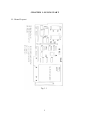
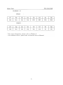
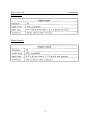
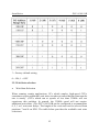
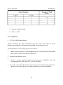
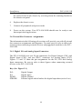
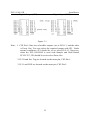
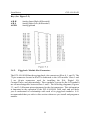
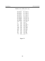
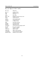
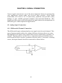
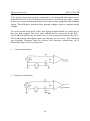
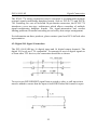
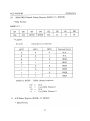
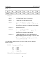
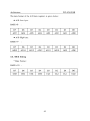
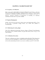
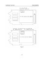
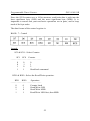
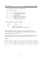
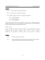
PCL-816/814B
MODULAR DA&C CARD
PCL-816/814B
MODULAR DA&C CARD
USER'S MANUAL
COPYRIGHT NOTICE
This document has been copyrighted, 1994, by Advantech Co., Ltd. All
rights are reserved. Advantech Co., Ltd. reserves the right to make
improvements to the products described in this manual at any time
without notice.
No part of this manual may be reproduced, copied, translated, or
transmitted in any form or by any means without the prior written
permission of Advantech Co., Ltd. Information provided in this manual is
intended to be accurate and reliable. However, Advantech Co., Ltd.
assumes no responsibility for its use, nor for any infringements upon the
rights of third parties which may result from its use.
ACKNOWLEDGEMENTS
PC-LabCard is a trademark of Advantech Co., Ltd. IBM and PC are
trademarks of International Business Machines Corporation.
MS-DOS is a trade mark of Microsoft Corporation. BASIC is a
trademark of Dartmouth College.
Part No. 2003816020. 2nd Edition
Printed in Taiwan. Nov. 1994
TABLE OF CONTENTS
CHARTER 1. QUICK START - - - - - - - - - - - - - - - - - - - - - - - - - - 1
1.1. Board Layout- - - - - - - - - - - - - - - - - - - - - - - - - - - - - - - - 1
1.2. Pin Connector Assignment - - - - - - - - - - - - - - - - - - - - - - - 2
1.3. Quick RUN- - - - - - - - - - - - - - - - -- - - - - - - - - - - - - - - - - 2
1.3.1. Factory Setting- - - - - - - - - - - - - - - - - - - - - - - - - - - 2
1.3.2. Run the PCL-TEST- - - - - - - - - - - - - - - - - - - - - - - - 3
1.4. Quick Reference for Register Format- - - - - - - - - - - - - 3
CHARTER 2. INTRODUCTION - - - - - - - - - - - - - - - - - - - - - - - - 7
2.1. General Information- - - - - - - - - - - - - - - - - - - - - - - - - - - - 7
2.2. Initial Inspection- - - - - - - - - - - - - - - - - - - - - - - - - - - - - - - 7
2.3. Specifications- - - - - - - - - - - - - - - - - - - - - - - - - - - - - - - - - 8
CHARTER 3. INSTALLATION - - - - - - - - - - - - - - - - - - - - - - - - - 11
3.1. Base Address Selection- - - - - - - - - - - - - - - - - - - - - - - - - - 11
3.2. Wait State selection- - - - - - - - - - - - - - - - - - - - - - - - - - - - - 12
3.3. Installation- - - - - - - - - - - - - - - - - - - - - - - - - - - - - - - - - - - 13
3.4. Pin and Slot Connector. Assignments - - - - - - - - - - - - - - - - 14
3.4.1. Digital I/O and Analog Input Connectors - - - - - - - - - 14
3.4.2. Piggyback Module Slot Connectors - - - - - - - - - - - - - 16
3.5. Software Disk- - - - - - - - - - - - - - - - - - - - - - - - - - - - - - - - - 21
CHARTER 4. SIGNAL CONNECTION- - - - - - - - - - - - - - - - - - - - 23
4.1. Analog Input Connection - - - - - - - - - - - - - - - - - - - - - - - - - 23
4.1.1. Differential Channel Connection - - - - - - - - - - - - - - - 23
4.2. Digital I/O Signal Connection - - - - - - - - - - - - - - - - - - - - - -23
CHAPTERER 5. ARCHITECTURE. - - - - - - - - - - - - - - - - - - - - - -27
5.1. Register Format- - - - - - - - - - - - - - - - - - - - - - - - - - - - - - 27
5.1.1. I/O Port Address Map- - - - - - - - - - - - - - - - - - - - - - 27
5.2. A/D Conversion Mode- - - - - - - - - - - - - - - - - - - - - - - - - - 41
5.3. A/D Data Format and Status Register- - - - - - - - - - - - - - - - 41
5.4. MUX Setting- - - - - - - - - - - - - - - - - - - - - - - - - - - - - - - - - 42
5.5. Gain Setting- - - - - - - - - - - - - - - - - - - - - - - - - - - - - - - - - - 43
5.6. Trigger Mode- - - - - - - - - - - - - - - - - - - - - - - - - - - - - - - - - 43
5.7. A/D Data Transfer- - - - - - - - - - - - - - - - - - - - - - - - - - - - - - 44
5.8. How to Execute an A/D Conversion - - - - - - - - - - - - - - - - - 45
i
CHAPTER 6. CALIBRATION AND TEST- - - - - - - - - - - - - - - 6. 1. Frequency of Calibration- - - - - - - - - - - - - - - - - - - - - - 6.2. Required Equipment- - - - - - - - - - - - - - - - - - - - - - - - - 6.3. Calibrating the Analog Input - - - - - - - - - - - - - - - - - - - 6.3.1. Calibration Procedure - - - - - - - - - - - - - - - - - - - -
47
47
47
47
47
CHAPTER 7. TROUBLESHOOTING AND DIAGNOSIS - - - - - - 49
APPENDIX A. PROGRAMMABLE TIMER/COUNTER- - - - - - - 51
A.1. The Intel 8254- - - - - - - - - - - - - - - - - - - - - - - - - - - - - - - - 51
A.2. Counter Read/Write and Control Registers - - - - - - - - - - - - 51
A.3. Counter Operating Modes - - - - - - - - - - - - - - - - - - - - - - - - 55
A.3.1. MODE O - Stop on Terminal Count- - - - - - - - - - - - 55
A.3.2. MODE 1 - Programmable One-Shot- - - - - - - - - - - - 55
A.3.3. MODE 2 - Rate Generator (divide by N counter) - - - 55
A.3.4. MODE 3 - Square Wave Rate Generator - - - - - - - - - 56
A.3.5. MODE 4 - Software Triggered Strobe - - - - - - - - - - - 57
A.3.6. MODE 5 - Hardware Triggered Strobe- - - - - - - - - - -57
A.4. Counter Operations - - - - - - - - - - - - - - - - - - - - - - - - - - - - 57
A.4.1. Read/Write Operation- - - - - - - - - - - - - - - - - - - - - - 57
A.4.2. Counter Read-Back Command- - - - - - - - - - - - - - - - 58
A.4.3. Counter Latch Operation - - - - - - - - - - - - - - - - - - - 58
ii
CHAPTER 1. OUICK START
1.1. Board Layout
1
Quick Start
1.2. Pin Connector Assignment
PCL-816/814B
1.3. Quick RUN
1.3.1. Factory Setting
1.BaseAddress : 200(HEX)
2. Wait State : 0
2
PCL-816/814B
1.3.2. Run the PCL-TEST
Quick Start
1. Install the PCL-816/814B in your PC.
2. Insert the Utility disk in your disk driver.
3. Run the PCLTEST.EXE.
4. Connect the signal to an analog input on CN3 (Use of Screwterminal Board PCLD-880 is recommended).
1.4. Quick Reference for Register Format
1. BASE+0 (READ/WRITE) : Digital I/O Low Byte
2. BASE+1 (READ/WRITE) : Digital I/O High Byte
3. BASE+2
: N/A
4. BASE+3
: N/A
5. BASE+4 (READ/WRITE) : 8254 Counter0
6. BASE+5 (READIWRITE) : 8254 Counter 1
7. BASES+6 (READIWRITE) : 8254 Counter2
8. BASE+7 (READIWRITE) : 8254 Control Word
9. BASE+8
READ : A/D low byte data
WRITE : A/D software trig
10.BASE+9
READ : A/D high byte data
3
4
5
6
CHAPTER 2. INTRODUCTION
2.1. General Information
The PCL-816/814B is a 16-bit/l4-bit multi-purpose DAS (Data Acquisition
System) card. It provides great flexibility for PC-based data acquisition
systems by supporting a variety of piggyback DAS modules for Digital I/O,
Counter/Timer, D/A and A/D applications.
The PCL-8161814B DAS card comes equipped with its own 16-bit/l4-bit A/D
piggyback module. Additional modules may be purchased separately. We also
provide the following special function modules:
•
16-bit D/A module
•
12-bit D/A module
•
24-bit DI/O module
•
5-channel counter/timer module
2.2. Initial Inspection
As you unpack your PCL-816/814B, check to make sure that the following
items have been included:
1. PCL-816/814B Modularized DAS Carrier Board
2. l6-Bit A/D Module (PCL-81601), or 14-Bit A/D Module (PCL-81401)
3. Utility diskette containing the software driver demonstration programs and
language interfaces for C, C++, PASCAL and BASIC.
4. User's manual
When unpacking the PCL-816/814B, be sure that you avoid contact with
anything that may produce a static electrical discharge. Inspect the PCL816/814B and it’s A/D module for any defects, or for damage that may have
occurred during shipping and handling. Your PCL-816/814B has been
thoroughly inspected and tested before being shipped. If you find that this
product is defective or incomplete in any manner, contact your authorized
distributor or local dealer immediately.
7
Introduction
PCL-816/814B
2.3. Specifications
Analog Input:
• Channels
:
16 differential analog input channels
•
Resolution
:
16 bits (PCL-816)
14 bits (PCL-814B)
•
Sampling rate
:
100 KHz maximum
•
Accuracy
:
0.003% FS +1 LSB (PCL-816 A/D Module)
0.003% FS +1 LSB (PCL-814B A/D Module)
•
Input impedance :
> 10 MΩ
•
Connector
D37 Female Connector
:
Programmable Input Ranges:
•
Bipolar
PCL-816
PCL-814B
:
+/-10 V
+/-5 V
+/-2.5 V
+/-1.25 V
:
+5 V
+2.5 V
+1.25 V
+0.625 V
•
Unipolar
:
0 - +10 V
0 - +5 V
0 - +2.5 V
0 - +1.25 V
•
Trigger mode
:
Software, pacer and external trigger modes
available
8
PCL-816/814B
Digital Input:
Introduction
Digital Output.
9
10
CHAPTER 3. INSTALLATION
The PCL-816/814B was designed with ease of use in mind. The only
parameters that have to be set are the base address and the wait state. Unlike
other DA&C cards which contain many jumpers and switches that must be set
manually, all hardware functions of the PCL-816/814B are software
programmable.
3.1. Base Address Selection
•
I/O Port Address Selection
It is important to select an appropriate I/O port address for the PCL-816/814B,
in order to avoid conflicts which might occur during input/output operations on
the PC bus. The PCL-816/814B utilizes 16 consecutive I/O address locations
within the PC's bus architecture. Valid addresses (hexadecimal) range from 100
to 3FO. Some of these addresses may be used by devices which already exist
on the bus. Exceptional care should therefore be exercised when selecting the
appropriate I/O address for your PCL-816/814B.
An eight position DIP switch, SW1, allows you to set the PCL-816/814B's I/O
address (position 1 through 6). The factory default address setting is 200
(hexadecimal). The following table provides the necessary information to make
an appropriate address selection (A4 through A9 correspond to the address
lines of your PC bus).
11
Installation
PCL-816/814B
* = Factory default setting
0 = ON; 1 = OFF
3.2. Wait State selection
•
Wait State Selection
When running certain applications, PCs which employ high-speed CPUs
sometimes require additional wait states in order to insure that the data transfer
rate is steady. (CPUs which run at speeds of less than 33MHz will not
experience this problem. In general, the 33MHz speed will not require
additional wait states.) The PCL-816/814B can be configured to accommodate
0, 2, 3 or 5 wait state delays. The length of the wait state can be selected from
positions 7 and 8 on SW1. The table below provides the available wait state
selections.
12
PCL-816/814B
Installation
* = Factory default setting
0 = ON; 1 = OFF
3.3. Installation
•
PCL-816/814B Installation
Before installing the PCL-816/814B in the PC, make sure that the DAS
modules are properly configured and installed on the carrier board.
To install the PCL-816/814B, proceed as follows:
1.
Make sure that your PC and peripheral devices are powered off and that
their power cords have been disconnected.
2.
Remove the chassis cover.
3.
Locate a vacant expansion slot on your passive backplane that will
accommodate the full-sized PCL-816/814B board.
4. Insert the carrier board into the expansion slot. Use the retaining bracket as
a guide between the chassis rear panel and the base of the backplane.
13
Installation
PCL-816/814B
5. Once the PCL-816/814B is firmly inserted into the expansion slot, secure
the carrier board to the chassis by screwing down the retaining bracket to
the chassis rear panel.
6.
Replace the chassis cover.
7.
Connect all peripheral and power cords.
8.
Power on the system. Your PCL-816/814B should now be ready to run
data acquisition applications.
3.4. Pin and Slot Connector Assignments
The information in the following sub-sections will provide you with all pin and
slot connector assignments and diagrams. You may need to refer to these subsections when connecting external devices and piggyback modules to the PCL816/814B.
3.4.1. Digital I/O and Analog Input Connectors
The PCL-816/814B uses two 20-pin connectors for Digital Output (CN1) and
Digital Input (CN2), and one DB-37 connector for Analog Input (CN3).
Figures 3.1 and 3.2 show the pin assignments for the D/I, D/O and Analog
Input connectors. Be sure to refer to these figures when connecting external
devices to the PCL-816/814B.
Key: (for Figure 3-1)
D/O
D/I
DGND
STROBE
Digital Output
Digital Input
Digital Ground
External signal which latches the digital input data (active low)
14
PCL-816/814B
Digital Output (CNI)
Installation
Digital Input (CN2)
Figure 3.1
Note: 1. CNI Pin 14 has two selectable outputs: one is D/O 13, and the other
is Pacer Out. You can select the required output with JP1. Under
normal conditions, JP1 should be set to select D/O 13. However,
when the PCL-816/814B is used with Sample and Hold Board
PCLD-787, JP1 should be set to select Pacer Out.
2. D/I O and Ext. Trig are located on the same pin, CN2 Pin 1.
3. D/I 1 and POE are located on the same pin, CN2 Pin 2.
15
Installation
PCL-816/814B
Key: (for Figure 3-2)
A/D H
A/D L
AGND
3.4.2.
Analog Input High (differential)
Analog Input Low (differential)
Analog ground
Piggyback Module Slot Connectors
The PCL-816/814B has three piggyback slot connectors (Slots 0, 1, and 2). The
72-pin connector located at Slot 0 is dedicated to the A/D module. Slots 1 and
2 are 64-pin connectors used for installing the D/A, Digital I/O,
Counter/Timer, and other modules. These modules (except for the A/D module)
are all interchangeable between Slots 1 and 2. The following diagrams (Figures
3.3, and 3.4) illustrate pin assignments for the slot connectors. This information
is important to the operation of the PCL-816/814B DAS card, and will help
you to understand its relationship with each of its piggyback modules. It is
recommended that you refer to this section whenever you install and program a
module.
16
PCL-816/814B
Installation
Key: (for Figure 3.3: slot 0 )
A/D H0 - A/D H15
A/D L0 - A/D L15
AD0 - AD15
ID0 - ID3
A-D
PG0,PG1
U/B
ADTRIG
ADEOC
AGND
DGAND
Analog input high (differential)
Analog input low (differential)
A/D data bus
A/D module identification code
A/D channel selection
Gain selection
Unipolar/bipolar
A/D conversion trigger pulse
End of A/D conversion
Analog ground
Digital ground
17
Installation
PCL-816/814B
Slot 0 (for the A/D module only)
Figure 3.3
18
PCL-816/814B
Installation
Key: (for Figure 3.4: Slots 1 and 2)
D0 - D7
A0 - A3
SEL
IOR
IOW
ID0 - ID7
DRQ
IORY
CLKPC
CLK10
IRQ
AGND
DGND
ADTRIG
RESET
AEN
DMAEN
DMACK
CLR-IRQ
MODULSEL
Data bus
Address lines
Module active
I/O read
I/O write
Module identification code
DMA Request
I/O channel ready
Clock from PC
10 MHz clock
Interrupt request
Analog ground
Digital ground
A/D conversion trigger pulse
Reset the module
Address enable
DMA enable
DMA acknowledge
Clear interrupt request
Module select control
19
Installation
PCL-816/814B
Slots 1 and 2 (for all other modules)
Figure 3.4
20
PCL-816/814B
3.5.
Installation
Software Disk
A floppy disk containing utility software is included with each PCL-816/814B
to minimize your application programming effort, and support the PCL816/814B calibration. The utility programs include:
1.
A comprehensive I/O driver for A/D, D/A, Digital I/O and Counter
applications. This driver allows you to use standard functions, written in
common programming languages, to operate the PCL-816/814B without
going into detailed register control. Languages supported by the software
driver include BASICA, GWBASIC, QUICKBASIC, Microsoft C/C++
and PASCAL, Turbo C/C+ +, Borland C/C+ + and Turbo PASCAL.
Please refer to the Software Drivers User's Manual for more information.
2. Demonstration programs.
3. Calibration program.
4. Test program.
It is strongly recommended that you make a working copy from the master disk
and save the master disk in a safe place. You may use the DOS COPY or
DISKCOPY commands to copy the disk files to another floppy disk, or use the
COPY command to copy the files to a hard disk.
21
22
CHAPTER 4. SIGNAL CONNECTION
Correct signal connection is one of the most important factors in ensuring that
your application system sends and receives data correctly. Good signal
connections will avoid a lot of unnecessary problems and possible costly
damage to your valuable personal computer and associated hardware. This
chapter provides some useful information on signal connection arrangements in
different types of data acquisition applications.
4.1. Analog Input Connection
4.1.1. Differential Channel Connection
The differential input configuration has two signal wires for each channel. This
type of input responds only to the voltage difference between these two wires,
the High and Low inputs. If the signal source has no connection to ground, it is
called a "floating source". In this case, a connection must exist between Low
and Ground in order to define a common reference point. To measure a floating
source, the input channel should be connected as shown below:
23
Signal Connection
PCL-816/814B
If the signal source has one side connected to a local ground, the signal source
ground and the PCL-816/814B ground will not be at exactly the same voltage
as they are connected through the ground return of the equipment and building
wiring. The difference between these ground voltages forms a common mode
voltage.
To avoid ground loop noise effect, the signal ground should be connected to
the Low input signal. The Low input should not be connected to the PCL816/814B ground directly. In some cases, a wire connection between the PCL816/814B ground and signal source ground may be necessary. The following
two diagrams illustrate both the correct and incorrect connections for a
differential input with a local ground.
•
Correct connection:
•
Incorrect connection:
24
PCL-816/814B
Signal Connection
The PCLD-774 analog expansion board is designed to accommodate multiple
external signal-conditioning daughter boards, such as PCLD-779 and PCLD789. Featuring five sets of on-board 20-pin header connectors, the PCLD-774
introduces a new star-type architecture which allows cascading of multiple
signal-conditioning daughter boards. The signal-attenuation and currentloading problems of normal cascading are solved by this unique arrangement.
For information on these products, please contact your local PC-LabCard sales
representative.
4.2. Digital I/O Signal Connection
The PCL-816/814B has 16 digital input and 16 digital output channels. The
digital I/O levels are TTL compatible. To transmit or receive digital signals to
or from other TTL devices, the connection should be as shown:
To receive an OPEN/SHORT signal from a switch or relay, a pull-up resistor
must be added to ensure that the input is held HIGH when the contact is open.
25
26
CHAPTER 5. ARCHITECTURE
5.1. Register Format
This section has been written for those users who wish to design their own
software drivers, instead of using the one provided with the PCL-816/814B.
The following table provides a summary of the port address map. The
functions of each address and a detailed data format of each register are given
in the following section.
5.1.1.
I/O Port Address Map
Module
Location
Selected Read
Write
------------------------------------------------------BASE+0
Module-0 D/I Low Byte
D/O Low Byte
BASE+1
Module-0 D/I High Byte
D/O High Byte
BASE+2
Module-0 N/A
N/A
BASE+3
Module-0 N/A
N/A
BASE+4
Module-0 Counter 0
Counter 0
BASE+5
Module-0 Counter 1
Counter 1
BASE+6
Module-0 Counter 2
Counter 2
BASE+7
Module-0 Counter Readback
Counter Control
BASE+8
A/D Low Byte
Software A/D Trigger
BASE+9
A/D High Byte
A/D Range Control
BASE+10
Current Channel Status
Clear Interrupt Request
27
Architecture
PCL-816/814B
BASE + 11
MUX Scan Channel Status
Scan Channel Setting
BASE + 12
Control
Control
BASE + 13
Status
DMA/IRQ Channel Setting
BASE + 14
Carrier I.D. Code
Module Interrupt Mask
Control
BASE + 15
Module I.D. Code
Module Selection
1. Digital I/O Registers (BASE+0, 1; WRITE, READ)
The PCL-816/814B offers 16 digital input and 16 digital output channels.
These I/O channels use the input and output ports at addresses BASE+0
and BASE+1 (Module-0). The data format of each port is as follows:
* Data Format:
28
PCL-816/814B
Architecture
BASE+1(Write port) : D/O high byte
2.
8254 Counter Registers (BASE+4, 5, 6, 7; WRITE, READ)
BASE+4
8254 Counter #O Register
(Read/Write)
EASE+5
8254 Counter #1 Register (Read/Write)
BASE+6
8254 Counter #2 Register (Read/Write)
BASE+7
Counter Read-back Register (Read)
BASE+7
Counter Control Register
(Write)
The PCL-8161814B is equipped with an INTEL 8254 timer/counter chip. The
8254 has three counters. The PCL-816/814B uses counter #0 to generate the
trigger pulse for the A/D chip. Counter #0 should be programmed as Mode 1
(one-shot mode). The following instructions are recommended:
OUT BASE+7, &H32
;Set Counter #0 as Mode 1
OUT BASE+4, &H0A
;Write low byte first
OUT BASEI-4, 0
;Write high byte
(Program counter 0 as a 1 uS one-shot generator)
Note: Take care to program the 8254 counter 0 exactly as described in the
steps above, otherwise the PCL-816/814B will not perform the required data
acquisition tasks.
Counter #1 and Counter #2 are used to generate the pacer clock signal.
Programming the desired pacer clock rate is a simple procedure. The following
formula illustrates the pacer clock calculation:
29
Architecture
PCL-816/814B
Pacer rate = 10MHz/(C1*C2)
Where:
C1 = 16-bit data for Counter 1, Ranges 2 to 65535.
C2 = 16-bit data for Counter 2, Ranges 2 to 65535.
The manufacturer recommends using the following programming instructions
with the pacer clock rate:
OUT BASE+7, &H76
OUT BASE+S, C1_Low
OUT BASE+S, C1_High
OUT BASE+7, &HB6
OUT BASE+B, C2_Low
OUT BASE+6, C2_High
;Set Counter #1 as Mode 3
;Write C1's low byte
;Write C1's high byte
;Set Counter #2 as Mode 3
;Write C2's low byte
;Write C2's high byte
*** For more information about programming the Intel 8254 timer/counter,
please refer to Appendix A.
3.
A/D Data Registers (BASE+8, 9; READ)
*
Data Format:
30
PCL-816/814B
4.
Architecture
Software A/D Trigger (BASE+8; WRITE)
Any value written to the register BASE+8 will trigger the A/D module,
causing one data conversion.
* Please refer to Base+12 for Trigger Mode Setting.
5.
A/D Range Control (BASE+9, WRITE)
* Data Format:
31
Architecture
PCL-816/814B
PCL-816 16-BIT MODE CODING FORMAT
( FS = Full Scale Range)
When using our PCL-81401 14 Bit A/D Module, the data format for the A/D
Range Control byte is as follows:
32
PCL-816/814B
Architecture
Note: 1. When you want to assign the gain setting for a channel, you must use
Base+11 to assign the channel first.
2. For PCL-814B, unipolar and bipolar inputs cannot be mixed in autochannel scan mode. Input must be either all bipolar or unipolar.
33
Architecture
PCL-816/814B
6. Current A/D Channel Configuration Register (BASE+10; READ)
* Data Format:
BASE+10 :
* Legend:
UIB:
0 = Bipolar
1 = Unipolar
G1, G0:
Gain selection (refer to BASE+9)
CN3 to CN0:
Current channel number
7. Clear INT register (BASE+10; WRITE)
Any value written to the register BASE+10 will clear the interrupt active
flag. The PC-816/814B is then ready to accept the next interrupt request.
8. MUX Scan Register (BASE+11; WRITE, READ)
* Data Format:
BASE + 11 :
* Legend:
CH3 to CH0 - Stop scan channel number.
34
PCL-816/814B
Architecture
CL3 to CL0 - Start scan channel number
9. Control register (BASE+12, WRITE, READ)
* Data Format:
BASE+12 :
* Legend:
S/W
=
1, S/W trig enable
S/W
=
0, S/W trig disable
PACER
=
1, PACER trig enable
PACER
=
0, PACER trig disable
EXT
=
1, EXT. trig enable
EXT
=
0, EXT. trig disable
( Note : EXT. trig comes from DI0 )
POE
:
Pacer out enable control
POE
=
0, Pacer enabled
POE
=
1, Pacer is controlled by DI1. If DI1 is
connected to TTL low level, the Pacer
will be held. This means that the analog
source cannot go into A/D conversion.
35
Architecture
PCL-816/814B
Under normal conditions, DI1 will be
pulled high.
DMAEN
:
DMA transfer control
DMAEN
=
0, DMA transfer dis abled
DMAEN
=
1, DMA transfer enabled
Note:
When the DMA transfer function is
enabled, the INT for Terminal Count
(TC) only is also automatically enabled.
The DMA's terminal count generates
INT when the specified number of
bytes have been transferred.
INTE
:
Disable/Enable PCL-816/814B to
generate interrupt.
INTE
=
0, disables the function of interrupts.
No interrupt signal can be sent to the
PC bus.
INTE
=
1, enables the function of an interrupt
when any module sends an interrupt
signal .
DS1 to DS0 - DMA Source Selected
0 0 : A/D module
0 1 : Piggyback Module #1
1 0 : Piggyback Module #2
1 1 : invalid
36
37
Architecture
PCL-816/814B
BASE + 13
* Legend:
DRDY
:
A/D Data Ready Flag of a Conversion
DRDY
=
1, means the A/D data has been read.
DRDY
=
0, means the A/D data is ready for reading.
(When you read the Base+8 or Base+9, then this bit
will be set to 1 until new A/D Data has been loaded).
INTACT :
Interrupt active flag
INTACT =
0, means the PCL-816/814B has not generated an
interrupt. If the INT function is enabled, then this
function will be waiting for an interrupt.
INTACT =
1, means that if the PCL-816/814B generates an
interrupt, then this bit will be set to 1. INTACT must
be cleared to 0 before accepting the next interrupt.
This is accomplished by writing any value to base
+10 of the PCL-816/814B.
You can find the interrupt source by way of reading ISI, IS0 (Interrupt
Source ID Code).
IS1, IS0
: Interrupt source ID code.
00
01
10
11
:
:
:
:
Slot 0
Slot 1
Slot 2
DMA (TC)
CN3 to CN0 : Next channel to be converted.
38
PCL-816/814B
Architecture
12. Carrier Board ID Code Register (BASE+14, READ)
* Data Format
BASE+14 :
You can get the Carrier Board ID Code by reading BASE+14 twice. If on
the first reading, the byte you got was 81 (HEX), then the second byte will
be 60 (HEX). On the other hand, if the first byte you got was 60 (HEX),
then the second byte will be 81 (HEX).
13. Module Interrupt Mask Setting (BASE+14, WRITE)
* Data Format
BASE + 14 :
* Legend :
M0 :
Slot 0 interrupt mask bit.
M0 =
0, Slot 0 interrupt function enabled.
M0 =
1, Slot 0 interrupt function disabled.
M1 :
Slot 1 interrupt mask bit.
M1 =
0, Slot 1 interrupt function enabled.
M1 =
1, Slot 1 interrupt function disabled.
39
Architecture
PCL-816/8I4B
M2 :
Slot 2 interrupt mask bit.
M2 =
0, Slot 2 interrupt function enabled.
M2 =
1, Slot 2 interrupt function disabled.
14. Module ID Code Register (BASE+15, READ)
* Data Format:
BASE + 15 :
* Legend:
ID3 to ID0 - Active module identify code.
40
PCL-816/814B
Architecture
15. Module Selection register (BASE+15, WRITE)
The Module Select register is a write-only register using address
BASE+1S. This register can select the active module on the
PCL-816/814B.
* Data Format:
BASE+15 :
S1 S0
Selected Module
-----------------------------0
0 On board A/D module
0
1
GP Module 1
1
0
GP Module 2
1
1
Not available
5.2. A/D Conversion Mode
This section provides a complete explanation of how to use the PCL-8161814B
A/D conversion functions. The following topics are covered: A/D data format,
input range selection, MUX multiplexer channel control, trigger modes and
data transfer.
5.3. A/D Data Format and Status Register
An 8 bit register is too small to accommodate 16/14 bit A/D conversions
performed by the PCL-816/814B. This problem is solved by storing A/D data
in two 8-bit registers located al addresses BASE +8 and BASE +9. The A/D
low byte data are located in positions D0 (AD0) through D7 (AD7) of BASE
f8. A/D high byte data are located in positions D0 (AD8) through D7 (AD15)
of BASE +9. The least significant bit is AD0, and the most significant bit is
AD15.
41
42
PCL-81 6/814B
5.5. Gain Setting
Architecture
* Data Format :
BASE+B
5.6. Trigger Mode
The PCL-816/814B A/D conversions can be triggered in any one of three ways:
software trigger, on-board programmable pacer or external pulse trigger. Each
is explained below:
1. Software trigger
This feature is controlled by software commands issued by the application
program. Writing to register BASE +8 with any value causes a software
trigger to be executed. This mode is not normally used in high speed A/D
applications, due to the short execution times of the application programs.
2. On-board programmable pacer
The PCL-816/814B incorporates the INTEL 8254 Programmable Interval
Timer/Counter. In the pacer trigger mode, Counters 1 and 2 of the INTEL
8254 are configured as one pacer, offering precisely timed A/D converter
trigger pulses. Speeds range between 0.5 MHz and 35 minutes per pulse (For
details on how to use the INTEL 8254 timer/counter, please refer to
Appendix A). The pacer trigger mode is ideal for interrupt and DMA data
transfer, which is normally used in A/D applications requiring high
conversion speeds.
3. External pulse trigger
The PCL-816/814B direct external trigger pulses are controlled through
EXT.TRG (connector CN2 DI0). This mode is used mostly in A/D
applications requiring A/D conversions which are not measured
43
Architecture
PCL-816/814B
periodically. Instead, they are measured conditionally (e.g., in thermocouple
temperature control).
5.7. A/D Data Transfer
There are three possible ways to execute the PCL-816/814B A/D data transfer:
(1) Program control (2) Interrupt routine and (3) Direct memory access.
1. Program control
The program control method of data transfer uses the "polling" concept, in
which each device is checked to see if data is to be transferred. After the
A/D converter has been triggered, the application program checks the data
ready (DRDY) bit of BASE + 13. If the DRDY bit is 0, the converted data
is moved from the A/D data register to computer memory by application
program control.
2. Interrupt routine
When employing the interrupt routine method of transfer, data is sent from
the A/D data registers to a previously defined memory segment by the
interrupt service routine. At the start of each conversion, the A/D Trigger
signal generates an interrupt which enables the interrupt service routine to
perform the transfer. Before using this interrupt routine, the following
parameters must be specified:
a. The interrupt control bit of the control register (BASE +12).
b. The IRQ level selection BASE +13.
A write action to the A/D status register address (BASE +10) with any
value resets the PCL-816/814B interrupt request and re-enables the PCL816/813B interrupt.
3. Direct memory access (DMA)
DMA transfers A/D data from the PCL-816/814B hardware device to the
PC system memory without operating the system CPU. DMA is very
useful in high speed data transfer, but is complicated to operate. It is
necessary to
44
PCL-816/814B
Architecture
set the DMA channel selection (BASE +13), the DMA enable bit in the
PCL-816/814B control register (BASE +12) and the 8237 DMA controller
registers before performing DMA operations. We recommend that the
PCL-816/814B software driver be used for DMA operation. For more
information regarding DMA operations, please refer to any data book for
the 8237 DMA controller.
5.8. How to Execute an A/D Conversion
I/O port instructions used by D&A programs may be written either directly or
by first invoking the PCL-816/814B driver. The latter approach is
recommended, as it enhances program performance and makes programming
easier. In the last section of this chapter, step-by-step implementation
procedures for different AD operations are outlined.
Data transfer using the methods of pacer trigger and program control may be
accomplished without the PCL-816/814B driver, as follows:
Step 1 : Set the input channel by specifying the Mux scan range.
Step 2 : Write the pacer trigger mode to the control register, Base + 12.
Step 3 : Wait for the DRDY by reading the BASE +13 register DRDY bit.
Step 4 : Read data from the A/D converter by reading the A/D data
registers (BASE +8 and +9).
Step 5 : Convert data by converting the binary A/D data to an integer.
45
46
CHAPTER 6. CALIBRATION AND TEST
6.1. Frequency of Calibration
Since every card is thoroughly tested and calibrated in our factory, your new
PCL-816/814B should not require calibration before initial use. Under normal
conditions, a calibration should be performed every 6 months to one year; if,
however, frequent variations in temperature or humidity are common,
recalibrate at least once every three months.
6.2. Required Equipment
Ideally, you will need a precision voltage source and connecting cables. If you
do not have a precision voltage source, our 16-Bit D/A module is
recommended.
6.3. Calibrating the Analog Input
The A/D is calibrated by applying a known voltage to Channel 0 and adjusting
the onboard VRs (variable resistors) for gain and offset (refer to Fig 6.1 for
VRs location).
6.3.1. Calibration Procedure
The entire calibration procedure is included on the utility disk. The information
can be accessed by running the CALB816.EXE/CALB814B.EXE file. Please
refer to this automated procedure if you want to calibrate your PCL-816/814B.
47
48
CHAPTER 7. TROUBLESHOOTING AND DIAGNOSIS
Should problems arise when using the PCL-816/814B MODULARIZED
DA&C CARD, the following list of troubleshooting procedures should be
helpful in identifying the cause and implementing a solution.
( 1) Check the PC bus power, especially the +12 volt and +5 volt
supplies.
(2) Check the voltage of the signal between the AIHn and AILn. This
voltage should not exceed the full scale input range of the card.
(3) Check the voltage between your signal ground and the card's ground.
It should be 0 volts.
(4) Check other boards in your PC for Address, DMA and Interrupt level
conflicts.
(5) Refer to our example programs on the utility disk for techniques and
as a guide to check your programs again.
49
50
APPENDIX A. PROGRAMMABLE TIMER/COUNTER
A.1.The Intel 8254
The PCL816/814B uses the Inlet 8254 programmable interval timer/ counter
Version 2. The 8254 is a very popular timer/counter device consisting of three
independent 16 bit down counters. Each counter has a clock input, control gate
and an output Ii can be programmed to have a count from 2 up to 65535.
The maximum clock input frequency is 10 MHz for Version 2 of the 8254.
The PCL8161814B provides a 10 MHz input frequency through an on-board
crystal oscillator.
Counters 1 and 2 are cascaded and operated in a tired divider configuration.
Counter 1 input is connected to tire 10 MHz input frequency and the output of
Counter 1 is connected to the input of Counter 2. The output of Counter 2 is
internally configured to provide trigger pulses to the A/D converter, but it is
also available for other uses. CNI Pin 13 may he configured as either DO13 or
Pacer Out by means of jumper JP1.
A.2. Counter. Read/Write and Control Registers
The 8254 programmable interval timer uses four registers at address BASE+4,
BASE+5, BASE+6 and BASE+7. The function of each register is as follows:
BASE+4
Counter 0 Read/Write
BASF+5
Counter 1 Read/Write
BASE+6
Counter 2 Read/Write
BASE+7
Counter Control Word
51
Programmable Timer/Counter
PCL-816/814B
Since the 8254 counter uses a 16 bit structure, read/write data is split into the
least significant byte (LSB) and the most significant byte (MSB). It is
important to ensure that your read/write operations are in pairs, and to keep
track of the byte order.
The data format of the control register is:
BASE+ 7 : Control
Legend :
SCI & SCO - Select Counter
SC1 SC0 Counter
------------------------0
0
0
0
1
1
1
0
2
1
1
Read-back command
RW1 & RW0 - Select the Read/Write operation.
RW1 RW0
Operation
------------------------0
0
Counter latch
0
1
Read/Write LSB
1
0
Read/Write MSB
1
1
Read/Write LSB first, then MSB.
52
PCL-816/814B
Programmable Timer/Counter
M2, M1 and M0 - Select the Operating Mode.
M2 M1 M0 Mode
----------------------0
0
0
0 Interrupt on terminal count
0
0
1
1 Programmable one shot
X
1
0
2 Rate generator
X
1
1
3 Square wave rate generator
1
0
0
4 Software triggered strobe
1
0
1
5 Hardware triggered strobe
BCD - Select Binary or BCD Counting
BCD
Type
-----------------------------0
Binary Counter 16-bits
1
Binary Coded Decimal (BCD) Counter
If the module is set to binary, the count can be any number from 0 up to
65535. If the module is set to BCD (binary coded decimal), the count can be
set as any number from 0 to 9999
If both the SC1 and SC0 bit are set to 1, the counter control register is in readback command. The data format of the control register then becomes:
BASE+ 7
53
Programmable Timer/Counter
PCL-816/814B
Legend :
CNT = 0 - Latch count of selected counter(s).
STA = 0 Latch status of selected counter(s).
C2, CI and C0 Select counter for a read-back operation
C2 = 1 select Counter 2
C1 = 1 select Counter 1
C0 = 1 select Counter 0
It SCI and SC0 are both set to I and STA is set to 0. the counter read/write
register selected by C2 to C0 contains the return status byte. The data format
of the counter read/write register then becomes:
BASE + 4/5/6
Legend:
OUT -
Counter output current state.
NC
Null count indicates when the last count written to the counter
register has been loaded into the counting element.
-
54
PCL-816/814B
Programmable Timer/Counter
A.3. Counter Operating Modes
A.3.1. MODE 0 - Stop on Terminal Count
The output will he initially low alter setting this mode of operation. After the
count is loaded into the selected count register, the output will remain low and
the counter will count. When terminal count is reached, the output will go high
and will remain high until the selected counter is reloaded with the mode or a
new count is loaded. The counter continues to decrement after terminal count
has been reached. Rewriting a counter register during counting generates the
following results.
1.
2.
Write the first byte slops the current counting.
Write the second byte starts the new count.
A.3.2. MODE 1 - Programmable One-Shot
The output will go low on the count following the rising edge of the gate input.
The output will go high on the terminal count. If a new count value is loaded
while the output is low, it will not affect the duration of the one-shot pulse until
the succeeding trigger. The current count can be read at any time without
affecting the one-shot pulse. The one-shot is re-triggerable, thus the output will
remain low for the frill count after any rising edge on the gate input.
A.3.3. MODE 2 – Rate Generator (divide by N counter)
The output will he low for one period of the input clock The period from one
output pulse to the next equals the number of input counts in the counter
register. If the counter register is reloaded between output pulses, the present
period will not be affected, but the subsequent period will reflect the new value.
55
Programmable Timer/Counter
PCL-816/814B
The gate input, when low, will force the output high. When the gate input goes
high, the counter will start from the initial count. Therefore the gate input can
be used to synchronize the counter.
When this mode is set, the output will remain high until the count register is
loaded. The output can also be synchronized by software.
A.3.4. MODE 3 - Square Wave Kate Generator
Mode 3 is similar to Mode 2, except that the output will remain high until one
half the count has been completed (for even numbers), and will go low for the
other half of the count. This is accomplished by decrementing the counter by
two on the falling edge of each clock pulse. When the counter reaches the
terminal count, the state of the output is changed, the counter is reloaded with
the full count and the whole process is repeated.
If the count is odd and the output is high, the first clock pulse (after the count is
loaded ) decrements the count by 1. Subsequent clock pulses decrement the
count by 2. After timeout, the output goes low and the full count is reloaded.
The first clock pulse (following the reload) decrements the counter by 3.
Subsequent clock pulses decrement the count by two until timeout. Then the
whole process is repeated. In this way, if the count is odd, the output will he
high for (N+1)/2 counts and low for (N-1)/ 2 counts.
56
PCL-816/814B
Programmable Timer/Counter
A.3.5. MODE 4 - Software Triggered Strobe
After the mode is set, the output will be high. When the count is loaded, the
counter will begin counting. On terminal count, the output will go low for one
input clock period, after which it will again go high.
If the count register is reloaded during counting, the new count will be loaded
on the next CLK pulse. The count will be inhibited while the GATE input is
low.
A.3.6. MODE 5 - Hardware Triggered Strobe
The counter will start counting after the rising edge of the trigger input and will
go low for one clock period when the terminal count is reached. The counter is
retriggerable
A.4. Counter Operations
A.4.1. Read/Write Operation
For each counter, the type of read/write operation, operating mode and counter
type must all be properly specified in the control byte, and the control byte
must be written before the initial count is written.
Since the control byte register and all three counter read/write registers have
separate addresses, and each control byte specifies the counter it applies to (by
SC1 & SC0), no instructions on the operating sequence are required. Any
programming sequence following the 8254 conventions is acceptable.
There are three types of counter operation: read/load LSB, read/load MSB and
read/load LSB followed by MSB. It is important to ensure that your read/write
57
Programmable Timer/Counter.
PCL-816/814B
operations are in pairs, and to keep track or the byte order.
A.4.2, Counter Read-Bark Command
The 8254 counter read-back command allows users to check the count value,
programmed mode, and current states of the OUT pin and Null Count flag of
the selected counter(s). The command is written into the control word register
and has the format shown in Section 8.2.
The read-back command may be used to latch multiple counter output latches
by setting the CNT bit = 0 and selecting the desired counter(s) This single
command is functionally equivalent to several counter latch commands, one for
each counter latched.
The read-back command can also be used to latch status information of the
selected counter(s) by setting STA hit = 0. Status must be latched to be read;
the status of a counter is accessed by a read from that counter. The counter
status format is shown in Section 8.2
A.4.3. Counter Latch Operation
It is often desirable to read the value of a counter without disturbing the count
in progress. Usually the method used is the counter latch command method,
which allows the user to read the latched count value of the selected counter.
The 8254 supports counter latch operations in two ways. The first way is to set
RW1 & RW0 to (0.0), which latches the count of the selected counter in a 16
bit hold register. The second approach is performing latch operation under the
read-back command by setting SCI & SC0 to(l,l)and CNT = 0, This method
has the advantage of operating several counters at the same lime. A subsequent
read operation on the selected counter will retrieve the held value.
58